Embed Size (px)
Citation preview
ECE 340 Lecture 41 : MOSFET II
Class Outline: • Mobility Models • Short Channel Effects • Logic Devices
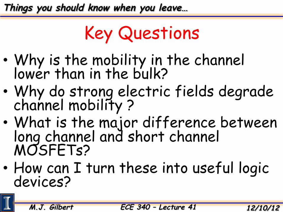
• Why is the mobility in the channel lower than in the bulk?
• Why do strong electric fields degrade channel mobility ?
• What is the major difference between long channel and short channel MOSFETs?
• How can I turn these into useful logic devices?
M.J. Gilbert ECE 340 – Lecture 41 12/10/12
Things you should know when you leave…
Key Questions
M.J. Gilbert ECE 340 – Lecture 41 12/10/12
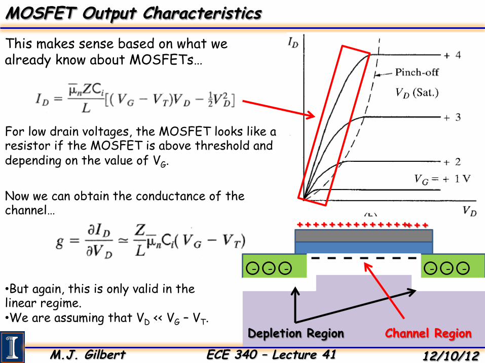
MOSFET Output Characteristics
This makes sense based on what we already know about MOSFETs…
For low drain voltages, the MOSFET looks like a resistor if the MOSFET is above threshold and depending on the value of VG.
Now we can obtain the conductance of the channel…
• But again, this is only valid in the linear regime. • We are assuming that VD << VG – VT.
++++ ++++++++++ + ++
- - - - - -
Depletion Region Channel Region
M.J. Gilbert ECE 340 – Lecture 41 12/10/12
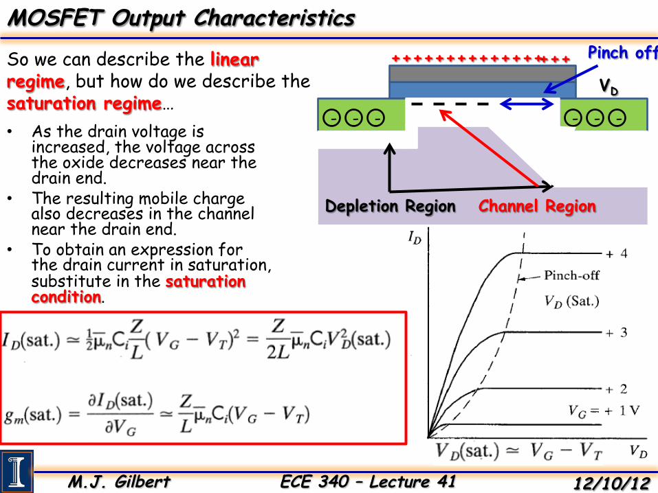
MOSFET Output Characteristics
So we can describe the linear regime, but how do we describe the saturation regime…
- - - - - -
Depletion Region
++++ ++++++++++ + ++ VD
Pinch off
Channel Region
• As the drain voltage is increased, the voltage across the oxide decreases near the drain end.
• The resulting mobile charge also decreases in the channel near the drain end.
• To obtain an expression for the drain current in saturation, substitute in the saturation condition.
M.J. Gilbert ECE 340 – Lecture 41 12/10/12
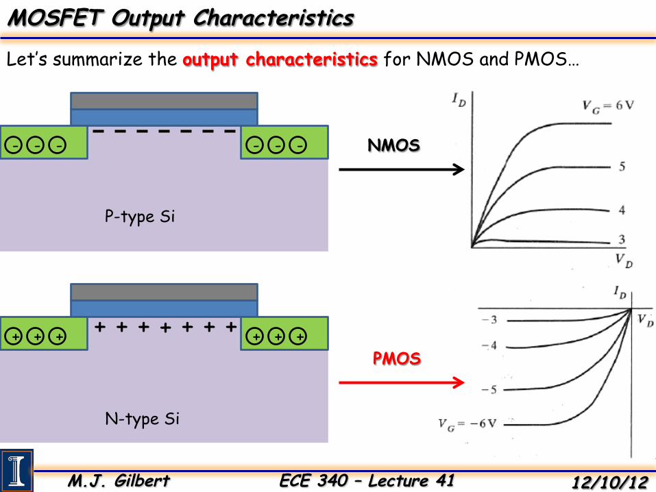
MOSFET Output Characteristics
Let’s summarize the output characteristics for NMOS and PMOS…
- - - - - -
P-type Si
+ + + + + + + + + + + + +
N-type Si
NMOS
PMOS
M.J. Gilbert ECE 340 – Lecture 41 12/10/12
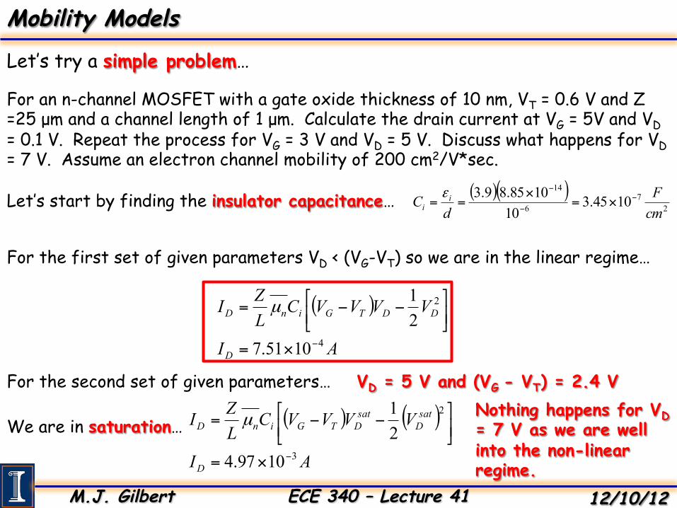
Mobility Models
Let’s try a simple problem…
For an n-channel MOSFET with a gate oxide thickness of 10 nm, VT = 0.6 V and Z =25 µm and a channel length of 1 µm. Calculate the drain current at VG = 5V and VD = 0.1 V. Repeat the process for VG = 3 V and VD = 5 V. Discuss what happens for VD = 7 V. Assume an electron channel mobility of 200 cm2/V*sec.
Let’s start by finding the insulator capacitance… ( )( )2
76
14
1045.310
1085.89.3cmF
dC ii
−−
−
×=×
==ε
For the first set of given parameters VD < (VG-VT) so we are in the linear regime…
( )
AI
VVVVCLZI
D
DDTGinD
4
2
1051.721
−×=
⎥⎦
⎤⎢⎣
⎡ −−= µ
For the second set of given parameters… VD = 5 V and (VG - VT) = 2.4 V
We are in saturation… ( ) ( )
AI
VVVVCLZI
D
satD
satDTGinD
3
2
1097.421
−×=
⎥⎦
⎤⎢⎣
⎡ −−= µ Nothing happens for VD = 7 V as we are well into the non-linear regime.
M.J. Gilbert ECE 340 – Lecture 41 12/10/12
Mobility Models
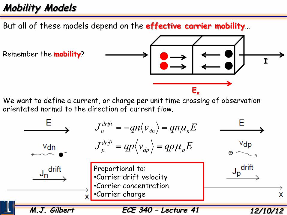
But all of these models depend on the effective carrier mobility…
Ex
I
We want to define a current, or charge per unit time crossing of observation orientated normal to the direction of current flow.
EqpvqpJ
EqnvqnJ
pdpdriftp
ndndriftn
µ
µ
==
=−=
Proportional to: • Carrier drift velocity • Carrier concentration • Carrier charge
Remember the mobility?
M.J. Gilbert ECE 340 – Lecture 41 12/10/12
Mobility Models
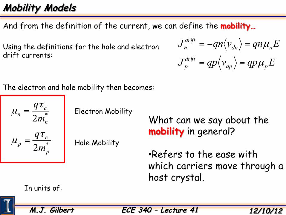
And from the definition of the current, we can define the mobility…
EqpvqpJ
EqnvqnJ
pdpdriftp
ndndriftn
µ
µ
==
=−=Using the definitions for the hole and electron drift currents:
The electron and hole mobility then becomes:
*
*
2
2
p
cp
n
cn
mqmq
τµ
τµ
=
= Electron Mobility
Hole Mobility
What can we say about the mobility in general? • Refers to the ease with which carriers move through a host crystal.
In units of:
M.J. Gilbert ECE 340 – Lecture 41 12/10/12
Mobility Models
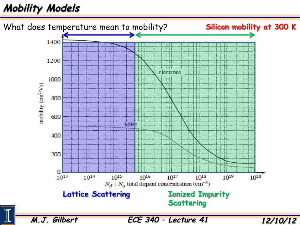
What does temperature mean to mobility? Silicon mobility at 300 K
Lattice Scattering Ionized Impurity Scattering
M.J. Gilbert ECE 340 – Lecture 41 12/10/12
Mobility Models
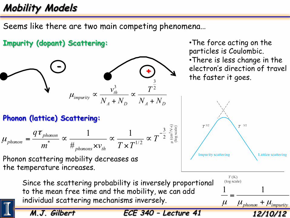
Seems like there are two main competing phenomena…
Impurity (dopant) Scattering:
- +
• The force acting on the particles is Coulombic. • There is less change in the electron’s direction of travel the faster it goes.
DADA
thimpurity NN
TNN
v+
∝+
∝23
3
µ
Phonon (lattice) Scattering:
23
2/1*
1#
1 −∝
×∝
×∝= T
TTvmq
thphonons
phononphonon
τµ
Phonon scattering mobility decreases as the temperature increases.
Since the scattering probability is inversely proportional to the mean free time and the mobility, we can add individual scattering mechanisms inversely.
impurityphonon µµµ +=
11
M.J. Gilbert ECE 340 – Lecture 41 12/10/12
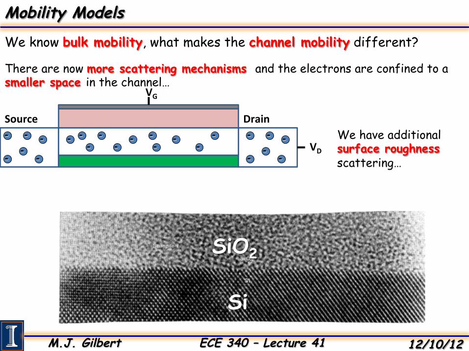
Mobility Models
We know bulk mobility, what makes the channel mobility different?
There are now more scattering mechanisms and the electrons are confined to a smaller space in the channel…
VG
-‐
-‐ -‐ -‐
-‐
-‐ -‐
-‐ -‐ -‐
-‐
-‐ -‐ -‐ -‐
-‐ -‐ -‐
-‐ -‐
-‐ -‐ -‐
Source Drain
VD
SiO2
Si
We have additional surface roughness scattering…
M.J. Gilbert ECE 340 – Lecture 41 12/10/12
Mobility Models
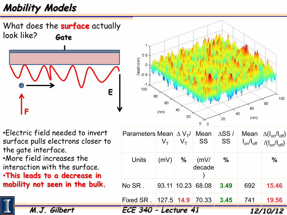
What does the surface actually look like?
Parameters Mean VT
∆ VT/ VT
Mean SS
∆SS / SS
Mean Ion/Ioff
∆(Ion/Ioff)
/(Ion/Ioff)
Units (mV) % (mV/decade
)
% %
No SR . 93.11 10.23 68.08 3.49 692 15.46
Fixed SR . 127.5 14.9 70.33 3.45 741 19.56
Gate
-‐ E
F
• Electric field needed to invert surface pulls electrons closer to the gate interface. • More field increases the interaction with the surface. • This leads to a decrease in mobility not seen in the bulk.

M.J. Gilbert ECE 340 – Lecture 41 12/10/12
Mobility Models
We are also aware of the fact that there can be stray charges present in the insulating oxide…
• Alkali metals can easily be incorporated in the oxide during the fabrication process.
• These metals induce positive charges in the oxides which induce negative charges in the semiconductor.
• The magnitude of the effect depends on the number of sodium atoms and their distance from the surface.
• The atoms may drift in applied fields which leads to a continuous change in the threshold voltage.
M.J. Gilbert ECE 340 – Lecture 41 12/10/12
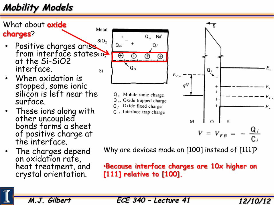
Mobility Models
What about oxide charges? • Positive charges arise
from interface states at the Si-SiO2 interface.
• When oxidation is stopped, some ionic silicon is left near the surface.
• These ions along with other uncoupled bonds forms a sheet of positive charge at the interface.
• The charges depend on oxidation rate, heat treatment, and crystal orientation.
Why are devices made on [100] instead of [111]? • Because interface charges are 10x higher on [111] relative to [100].
M.J. Gilbert ECE 340 – Lecture 41 12/10/12
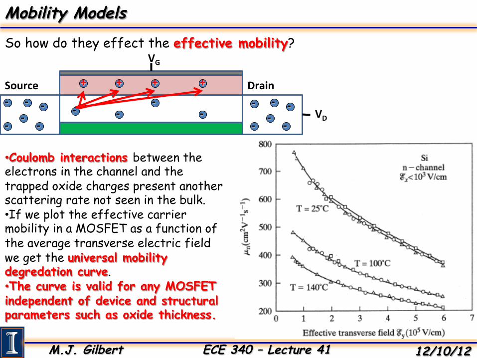
Mobility Models
So how do they effect the effective mobility? VG
-‐
-‐ -‐ -‐
-‐
-‐ -‐
-‐ -‐ -‐
-‐
-‐ -‐
-‐ -‐ -‐
Source Drain
VD
+ + + +
• Coulomb interactions between the electrons in the channel and the trapped oxide charges present another scattering rate not seen in the bulk. • If we plot the effective carrier mobility in a MOSFET as a function of the average transverse electric field we get the universal mobility degredation curve. • The curve is valid for any MOSFET independent of device and structural parameters such as oxide thickness.
M.J. Gilbert ECE 340 – Lecture 41 12/10/12
Mobility Models
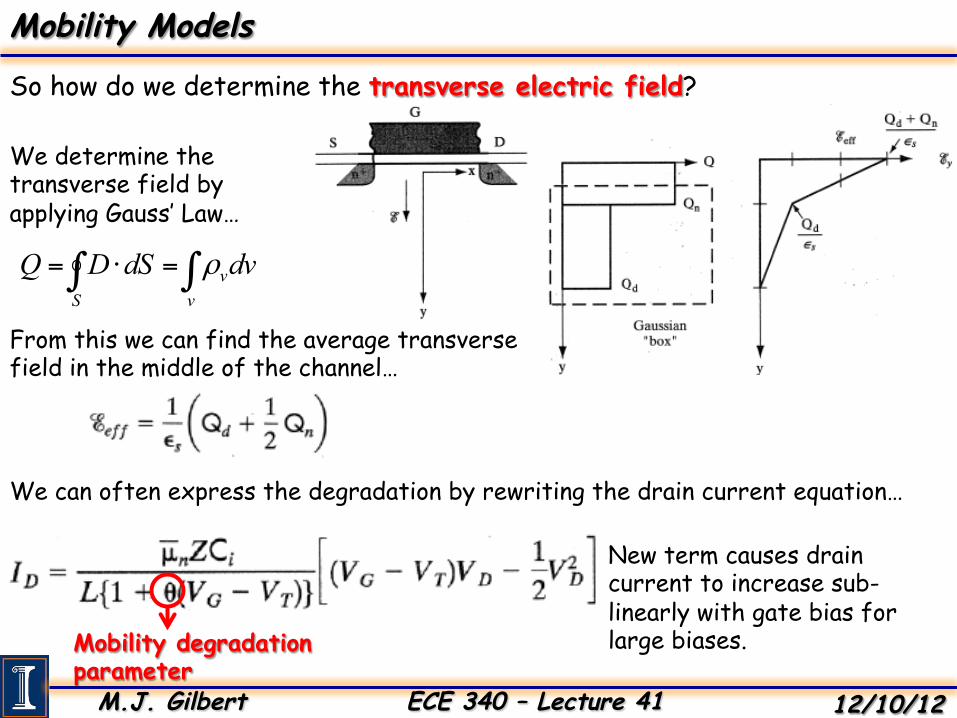
So how do we determine the transverse electric field?
We determine the transverse field by applying Gauss’ Law…
∫ ∫=⋅=S v
vdvdSDQ ρ
From this we can find the average transverse field in the middle of the channel…
We can often express the degradation by rewriting the drain current equation…
Mobility degradation parameter
New term causes drain current to increase sub-linearly with gate bias for large biases.
M.J. Gilbert ECE 340 – Lecture 41 12/10/12
Mobility Models
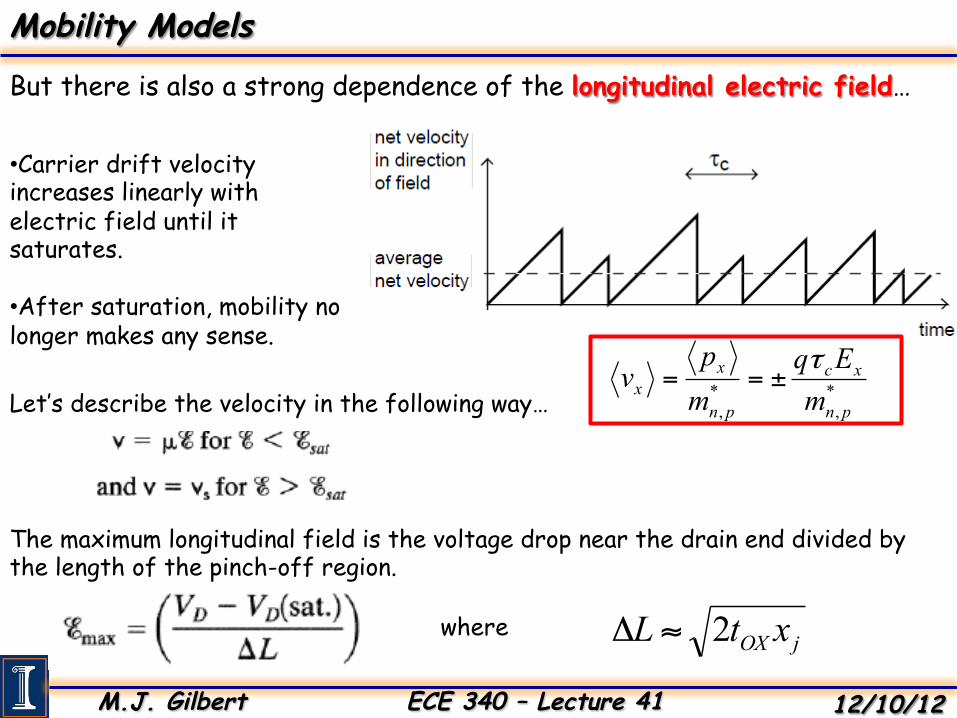
But there is also a strong dependence of the longitudinal electric field…
*,
*, pn
xc
pn
xx m
Eqmp
v τ±==
• Carrier drift velocity increases linearly with electric field until it saturates.
• After saturation, mobility no longer makes any sense.
Let’s describe the velocity in the following way…
The maximum longitudinal field is the voltage drop near the drain end divided by the length of the pinch-off region.
jOX xtL 2≈Δwhere
M.J. Gilbert ECE 340 – Lecture 41 12/10/12
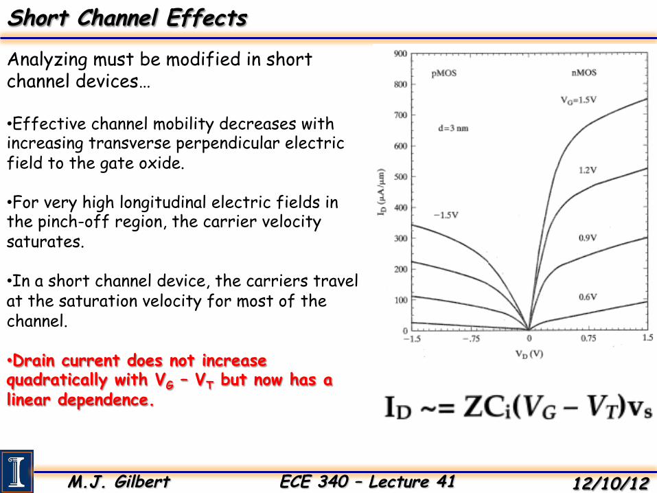
Short Channel Effects
Analyzing must be modified in short channel devices…
• Effective channel mobility decreases with increasing transverse perpendicular electric field to the gate oxide.
• For very high longitudinal electric fields in the pinch-off region, the carrier velocity saturates.
• In a short channel device, the carriers travel at the saturation velocity for most of the channel.
• Drain current does not increase quadratically with VG – VT but now has a linear dependence.
M.J. Gilbert ECE 340 – Lecture 41 12/10/12
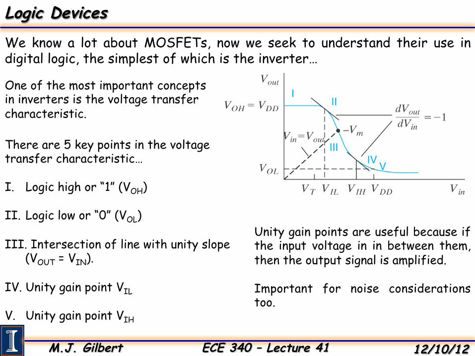
Logic Devices
We know a lot about MOSFETs, now we seek to understand their use in digital logic, the simplest of which is the inverter…
One of the most important concepts in inverters is the voltage transfer characteristic.
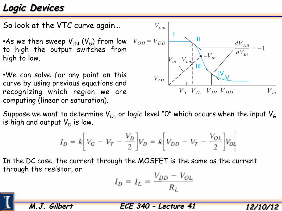
There are 5 key points in the voltage transfer characteristic… I. Logic high or “1” (VOH)
II. Logic low or “0” (VOL)
III. Intersection of line with unity slope (VOUT = VIN).
IV. Unity gain point VIL
V. Unity gain point VIH
Unity gain points are useful because if the input voltage in in between them, then the output signal is amplified. Important for noise considerations too.
M.J. Gilbert ECE 340 – Lecture 41 12/10/12
Logic Devices
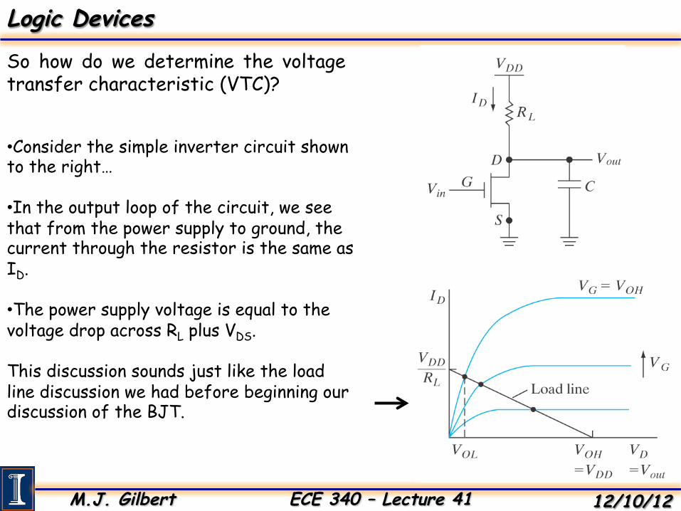
So how do we determine the voltage transfer characteristic (VTC)?
• Consider the simple inverter circuit shown to the right… • In the output loop of the circuit, we see that from the power supply to ground, the current through the resistor is the same as ID. • The power supply voltage is equal to the voltage drop across RL plus VDS. This discussion sounds just like the load line discussion we had before beginning our discussion of the BJT.
M.J. Gilbert ECE 340 – Lecture 41 12/10/12
Logic Devices
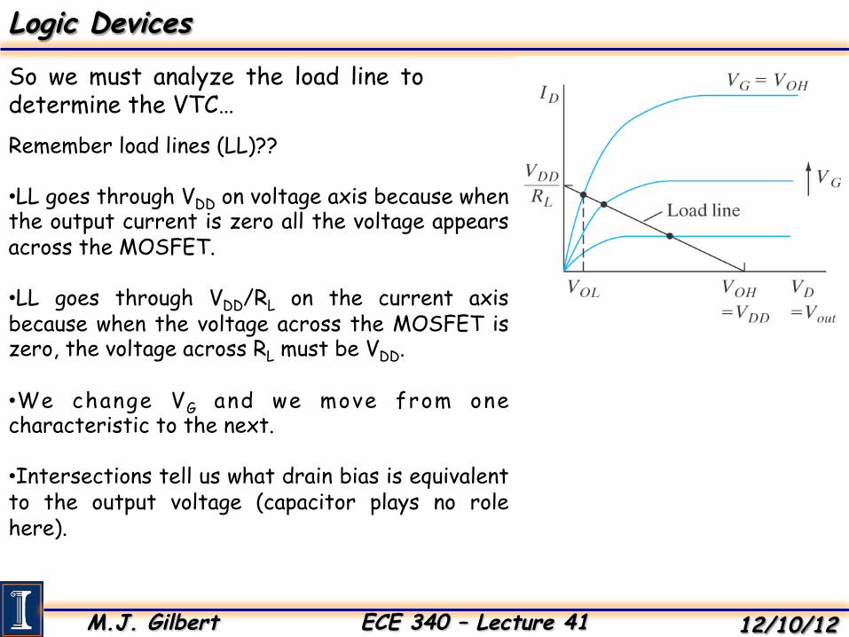
So we must analyze the load line to determine the VTC… Remember load lines (LL)?? • LL goes through VDD on voltage axis because when the output current is zero all the voltage appears across the MOSFET.
• LL goes through VDD/RL on the current axis because when the voltage across the MOSFET is zero, the voltage across RL must be VDD.
• We change VG and we move from one characteristic to the next.
• Intersections tell us what drain bias is equivalent to the output voltage (capacitor plays no role here).
M.J. Gilbert ECE 340 – Lecture 41 12/10/12
Logic Devices
So look at the VTC curve again…
• As we then sweep VIN (VG) from low to high the output switches from high to low. • We can solve for any point on this curve by using previous equations and recognizing which region we are computing (linear or saturation).
Suppose we want to determine VOL or logic level “0” which occurs when the input VG is high and output VD is low.
In the DC case, the current through the MOSFET is the same as the current through the resistor, or
M.J. Gilbert ECE 340 – Lecture 41 12/10/12
Logic Devices
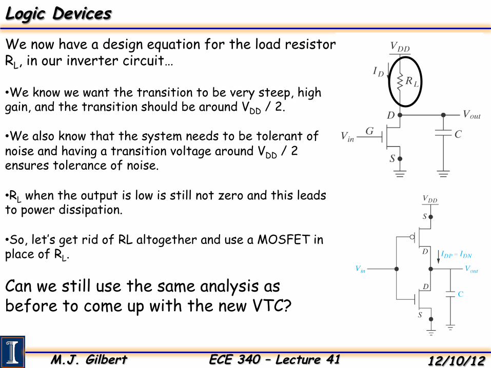
We now have a design equation for the load resistor, RL, in our inverter circuit…
• We know we want the transition to be very steep, high gain, and the transition should be around VDD / 2.
• We also know that the system needs to be tolerant of noise and having a transition voltage around VDD / 2 ensures tolerance of noise.
• RL when the output is low is still not zero and this leads to power dissipation.
• So, let’s get rid of RL altogether and use a MOSFET in place of RL.
Can we still use the same analysis as before to come up with the new VTC?
M.J. Gilbert ECE 340 – Lecture 41 12/10/12
Logic Devices
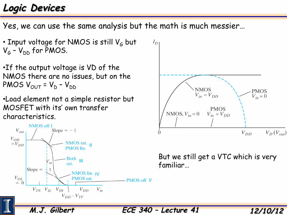
Yes, we can use the same analysis but the math is much messier…
• Input voltage for NMOS is still VG but VG – VDD for PMOS.
• If the output voltage is VD of the NMOS there are no issues, but on the PMOS VOUT = VD – VDD
• Load element not a simple resistor but MOSFET with its’ own transfer characteristics.
But we still get a VTC which is very familiar…
M.J. Gilbert ECE 340 – Lecture 41 12/10/12
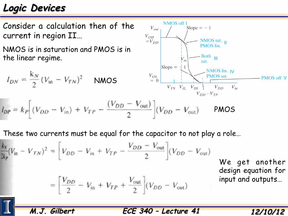
Logic Devices
Consider a calculation then of the current in region II… NMOS is in saturation and PMOS is in the linear regime.
NMOS
PMOS
These two currents must be equal for the capacitor to not play a role…
We get another design equation for input and outputs…


![2N7002BKV 60 V, 340 mA dual N-channel Trench MOSFET · 60 V, 340 mA dual N-channel Trench MOSFET 6. Thermal characteristics Table 6. Thermal characteristics [1] Device mounted on](https://img.dokumen.tips/doc/110x75/5b07051f7f8b9a5c308dc1d0/2n7002bkv-60-v-340-ma-dual-n-channel-trench-mosfet-v-340-ma-dual-n-channel-trench.jpg)