Embed Size (px)
Citation preview

Lecture 22:
Spring 2018
1
More CachesMeasuring Performance
ECE 2300Digital Logic & Computer Organization

Lecture 22:
Announcements
2
• HW7 due tomorrow 11:59pm
• Prelab 5(c) due Saturday 3pm
• Lab 6 (last one) released
• HW8 (last one) to be released tonight

Lecture 22:
Block address
Cache index
Hit/miss Cache contents after accessSet 0 Set 1
0 0 miss Mem[0]4 0 miss Mem[0] (*) Mem[4]2 0 miss Mem[2] Mem[4] (*)6 0 miss Mem[2] (*) Mem[6]8 0 miss Mem[8] Mem[6] (*)0 0 miss Mem[8] (*) Mem[0]4 0 miss Mem[4] Mem[0] (*)2 0 miss Mem[4] (*) Mem[2]6 0 miss Mem[6] Mem[2] (*)8 0 miss Mem[6] (*) Mem[8]2 0 miss Mem[2] Mem[8] (*)6 0 miss Mem[2] (*) Mem[6]2 0 hit Mem[2] Mem[6] (*)0 0 miss Mem[2] (*) Mem[0]
• 2-way set associative (*) = LRU block1 bit in this case
Another LRU Replacement Example
3Cold miss Conflict missColor code: Capacity miss

Lecture 22:
What About Writes?• Where do we put the result of a store?
• Cache hit (block is in cache)– Write new data value to the cache– Also write to memory (write through)– Don’t write to memory (write back)
• Requires an additional dirty bit for each cache block• Writes back to memory when a dirty cache block is evicted
• Cache miss (block is not in cache)– Allocate the line (bring it into the cache)
(write allocate)– Write to memory without allocation
(no write allocate or write around)4

Lecture 22:
• Assume write allocate• Size of each block is 8 bytes • Cache holds 2 blocks• Memory holds 8 blocks• Memory address
Write Through Example
2 tag bits1 index bit
3 byte offset bits
5
V tag data01

Lecture 22:
110
130
150160
180
200
220
240
Processor
R0R1R2R3
Memory
100
120
140
170
190
210
230
250
6
Cache
V tag data01
00
missM[000000] <= R0M[000100] <= R1M[010000] <= R2M[011100] <= R3
Write Through
333444555666
000000001001010010011011100100101101110110111111

Lecture 22:
110
130
150160
180
200
220
240
Processor
R0R1R2R3
Memory
100
120
140
170
190
210
230
250
7
Cache
V tag data01
10
miss
333444555666
110 100
Write Through
00
000000001001010010011011100100101101110110111111
M[000000] <= R0M[000100] <= R1M[010000] <= R2M[011100] <= R3

Lecture 22:
110
130
150160
180
200
220
240
Processor
R0R1R2R3
Memory
333
120
140
170
190
210
230
250
8
Cache
V tag data01
10
miss
333444555666
00 110 333
Write Through
000000001001010010011011100100101101110110111111
M[000000] <= R0M[000100] <= R1M[010000] <= R2M[011100] <= R3

Lecture 22:
110
130
150160
180
200
220
240
Processor
R0R1R2R3
Memory
333
120
140
170
190
210
230
250
9
Cache
V tag data01
10
hit
333444555666
00 110 333
Write Through
000000001001010010011011100100101101110110111111
M[000000] <= R0M[000100] <= R1M[010000] <= R2M[011100] <= R3

Lecture 22:
444
130
150160
180
200
220
240
Processor
R0R1R2R3
Memory
333
120
140
170
190
210
230
250
10
Cache
V tag data01
10
hit
333444555666
00 444 333
Write Through
000000001001010010011011100100101101110110111111
M[000000] <= R0M[000100] <= R1M[010000] <= R2M[011100] <= R3

Lecture 22:
444
130
150160
180
200
220
240
Processor
R0R1R2R3
Memory
333
120
140
170
190
210
230
250
11
Cache
V tag data01
10
333444555666
00 444 333miss
Write Through
000000001001010010011011100100101101110110111111
M[000000] <= R0M[000100] <= R1M[010000] <= R2M[011100] <= R3

Lecture 22:
444
130
150160
180
200
220
240
Processor
R0R1R2R3
Memory
333
120
140
170
190
210
230
250
12
Cache
V tag data01
10
333444555666
01 150 140miss
Write Through
000000001001010010011011100100101101110110111111
M[000000] <= R0M[000100] <= R1M[010000] <= R2M[011100] <= R3

Lecture 22:
444
130
150160
180
200
220
240
Processor
R0R1R2R3
Memory
333
120
555
170
190
210
230
250
13
Cache
V tag data01
10
333444555666
01 150 555miss
Write Through
000000001001010010011011100100101101110110111111
M[000000] <= R0M[000100] <= R1M[010000] <= R2M[011100] <= R3

Lecture 22:
444
130
150160
180
200
220
240
Processor
R0R1R2R3
Memory
333
120
555
170
190
210
230
250
14
Cache
V tag data01
10
333444555666
01 150 555miss
Write Through
000000001001010010011011100100101101110110111111
M[000000] <= R0M[000100] <= R1M[010000] <= R2M[011100] <= R3

Lecture 22:
444
130
150160
180
200
220
240
Processor
R0R1R2R3
Memory
333
120
555
170
190
210
230
250
15
Cache
V tag data01
11
333444555666
01 150 555miss01 170 160
Write Through
000000001001010010011011100100101101110110111111
M[000000] <= R0M[000100] <= R1M[010000] <= R2M[011100] <= R3

Lecture 22:
444
130
150160
180
200
220
240
Processor
R0R1R2R3
Memory
333
120
555
666
190
210
230
250
16
Cache
V tag data01
11
333444555666
01 150 555miss01 666 160
Write Through
000000001001010010011011100100101101110110111111
M[000000] <= R0M[000100] <= R1M[010000] <= R2M[011100] <= R3

Lecture 22:
• Assume write allocate• Size of each block is 8 bytes • Cache holds 2 blocks• Memory holds 8 blocks• Memory address
Write Back Example
2 tag bits1 index bit
3 byte offset bits
17
V D tag data01
Dirty bit

Lecture 22:
110
130
150160
180
200
220
240
Processor
R0R1R2R3
Memory
100
120
140
170
190
210
230
250
18
Cache
V D tag data01
00
missM[000000] <= R0M[000100] <= R1M[010000] <= R2M[011100] <= R3
Write Back
333444555666
00
000000001001010010011011100100101101110110111111

Lecture 22:
110
130
150160
180
200
220
240
Processor
R0R1R2R3
Memory
100
120
140
170
190
210
230
250
19
Cache
V D tag data01
10
miss
Write Back
333444555666
00 110 10000
000000001001010010011011100100101101110110111111
M[000000] <= R0M[000100] <= R1M[010000] <= R2M[011100] <= R3

Lecture 22:
110
130
150160
180
200
220
240
Processor
R0R1R2R3
Memory
100
120
140
170
190
210
230
250
20
Cache
V D tag data01
10
miss
Write Back
333444555666
00 110 33310
000000001001010010011011100100101101110110111111
M[000000] <= R0M[000100] <= R1M[010000] <= R2M[011100] <= R3

Lecture 22:
110
130
150160
180
200
220
240
Processor
R0R1R2R3
Memory
100
120
140
170
190
210
230
250
21
Cache
V D tag data01
10
Write Back
333444555666
00 110 33310
hit
000000001001010010011011100100101101110110111111
M[000000] <= R0M[000100] <= R1M[010000] <= R2M[011100] <= R3

Lecture 22:
110
130
150160
180
200
220
240
Processor
R0R1R2R3
Memory
100
120
140
170
190
210
230
250
22
Cache
V D tag data01
10
Write Back
333444555666
00 444 33310
hit
000000001001010010011011100100101101110110111111
M[000000] <= R0M[000100] <= R1M[010000] <= R2M[011100] <= R3

Lecture 22:
110
130
150160
180
200
220
240
Processor
R0R1R2R3
Memory
100
120
140
170
190
210
230
250
23
Cache
V D tag data01
10
Write Back
333444555666
00 444 33310
miss
000000001001010010011011100100101101110110111111
M[000000] <= R0M[000100] <= R1M[010000] <= R2M[011100] <= R3

Lecture 22:
444
130
150160
180
200
220
240
Processor
R0R1R2R3
Memory
333
120
140
170
190
210
230
250
24
Cache
V D tag data01
10
Write Back
333444555666
00 444 33310
miss
000000001001010010011011100100101101110110111111
M[000000] <= R0M[000100] <= R1M[010000] <= R2M[011100] <= R3

Lecture 22:
444
130
150160
180
200
220
240
Processor
R0R1R2R3
Memory
333
120
140
170
190
210
230
250
25
Cache
V D tag data01
10
Write Back
333444555666
01 150 14000
miss
000000001001010010011011100100101101110110111111
M[000000] <= R0M[000100] <= R1M[010000] <= R2M[011100] <= R3

Lecture 22:
444
130
150160
180
200
220
240
Processor
R0R1R2R3
Memory
333
120
140
170
190
210
230
250
26
Cache
V D tag data01
10
Write Back
333444555666
01 150 55510
miss
000000001001010010011011100100101101110110111111
M[000000] <= R0M[000100] <= R1M[010000] <= R2M[011100] <= R3

Lecture 22:
444
130
150160
180
200
220
240
Processor
R0R1R2R3
Memory
333
120
140
170
190
210
230
250
27
Cache
V D tag data01
10
Write Back
333444555666
01 150 55510
miss
000000001001010010011011100100101101110110111111
M[000000] <= R0M[000100] <= R1M[010000] <= R2M[011100] <= R3

Lecture 22:
444
130
150160
180
200
220
240
Processor
R0R1R2R3
Memory
333
120
140
170
190
210
230
250
28
Cache
V D tag data01
11
Write Back
333444555666
01 150 55510
miss01 170 160
000000001001010010011011100100101101110110111111
M[000000] <= R0M[000100] <= R1M[010000] <= R2M[011100] <= R3

Lecture 22:
444
130
150160
180
200
220
240
Processor
R0R1R2R3
Memory
333
120
140
170
190
210
230
250
29
Cache
V D tag data01
11
Write Back
333444555666
01 150 55511
miss01 666 160
000000001001010010011011100100101101110110111111
M[000000] <= R0M[000100] <= R1M[010000] <= R2M[011100] <= R3

Lecture 22:
Cache Hierarchy
30
• Time to get a block from memory is so long that performance suffers even with a low miss rate
• Example: 3% miss rate, 100 cycles to main memory – 0.03 × 100 = 3 extra cycles on average to access
instructions or data
• Solution: Add another level of cache

Lecture 22:
Pipeline with a Cache Hierarchy
31
ALU
Fm … F0
MUX
MD
PC
PCL
MUX
PCJD_IN
+2 Adder
IF/ID ID/EX EX/MEM MEM/WB
Decoder
SE
L1Instr
Cache(KB)
MB
MUX
MUX
MUX
MUX
MUX
LDSASBDR
D_in
RF
L1Data
Cache(KB)
L2 Cache (MB)
Main Memory (GB)

Lecture 22:
Cache Hierarchy
32
• Level 1 (L1) instruction and data caches – Small, but very fast
• Level 2 (L2) cache handles L1 misses – Larger and slower than L1, but much faster than main memory – L1 data are also present in L2
• Main memory handles L2 cache misses
• Example: assume 1 cycle to access L1 (3% miss rate), 10 cycles to L2, 10% L2 miss rate, 100 cycles to main memory– How many cycles on average for instruction/data access?
1 + 0.03 × (10 + 0.1 × 100) = 1.6 cycles

Lecture 22:
How Do We Measure Performance?• Execution time: The time between the start and
completion of a program (or task)
• Throughput: Total amount of work done in a given time
• Improving performance means – Reducing execution time, or – Increasing throughput
33

Lecture 22:
CPU Execution Time• Amount of time the CPU takes to run a program
• Derivation
34
number of instructionsin the program
average number ofcycles per instruction
clock cycle time (1/frequency)

Lecture 22:
Instruction Count (I)• Total number of instructions in the given
program
• Factors – Instruction set– Mix of instructions chosen by the compiler
35

Lecture 22:
Cycle Time (CT)• Clock period (1/frequency)
• Factors– Instruction set– Structure of the processor and memory hierarchy
36

Lecture 22:
Cycles Per Instruction (CPI)• Average number of cycles required to execute
each instruction
• Factors– Instruction set– Mix of instructions chosen by the compiler– Ordering of the instructions by the compiler– Structure of the processor and memory hierarchy
37

Lecture 22:
ADD R1,R2,R3
OR R4,R1,R3
SUB R5,R2,R1
AND R6,R1,R2
ADDI R7,R7,3
IM RegReg ALU
IM RegReg DMALU
IM RegReg DMALU
IM RegReg DMALU
IM RegReg DMALU
CC1 CC4 CC5 CC6 CC7 CC8 CC9CC2 CC3
DM
38
With forwarding: Reduced stall cyclesLower CPI, potentially reduced execution time
Processor Organization Impact on CPI (Example 1)
Lecture 22: 39
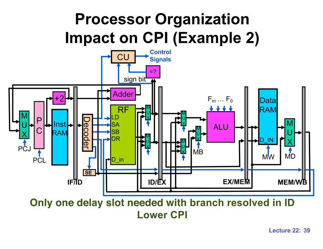
Processor Organization Impact on CPI (Example 2)
Only one delay slot needed with branch resolved in IDLower CPI
ControlSignals
ALU
Fm … F0
MUX
MD
CU
PC
PCL
MUX
PCJMW
D_IN
+2 Adder
IF/ID ID/EX EX/MEM MEM/WB
Decoder
SE
InstRAM
DataRAM
MB
MUX
MUX
MUX
MUX
MUX
LDSASBDR
D_in
RF
=?sign bit

Lecture 22: 40
OR R4,R1,R3
SUB R5,R2,R1
X: AND R6,R1,R2
IM RegReg ALU
IM RegReg DMALU
IM RegReg DMALU
IM RegReg DMALU
IM RegReg DMALU
CC1 CC4 CC5 CC6 CC7 CC8 CC9CC2 CC3
DM
ADDI R7,R7,3
BEQ R2,R3,X
...
NOP
Filling the branch delay slotwith a useful instruction
Compiler Impact on CPI (Example 3)
ADDI R7,R7,3

Lecture 22:
A Rough Breakdown of CPI
41
• CPIbase is the base CPI in an ideal scenario where instruction fetches and data memory accesses incur no extra delay
• CPImemhier is the (additional) CPI spent for accessing the memory hierarchy when a miss occurs in caches
• CPItotal is the overall CPI– CPItotal = CPIbase + CPImemhier

Lecture 22: 42
• With L1 caches– L1 instruction cache miss rate = 2%– L1 data cache miss rate = 4%– Miss penalty = 100 cycles (access main memory)– 20% of all instructions are loads, 10% are stores
• CPImemhier = 0.02 × 100 + 0.3 × 0.04 × 100 = 3.2
Impact of L1 Caches

Lecture 22:
Impact of L1+L2 Caches• With L1 and L2 caches
– L1 instruction cache miss rate = 2%– L1 data cache miss rate = 4%– L2 access time = 15 cycles– L2 miss rate = 25%– L2 miss penalty = 100 cycles (access main memory)– 20% of all instructions are loads, 10% are stores
• CPImemhier = 0.02 × (15 + 0.25 × 100) + 0.30 × 0.04 × (15 + 0.25 × 100) = 1.28
43

Lecture 22:
Before Next Class • H&H 8.4
Next Time
Virtual Memory
44


