Embed Size (px)
Citation preview

E4332: VLSI Design Laboratory
Nagendra KrishnapuraColumbia University
Spring 2005: [email protected]
1Nagendra Krishnapura: VLSI Design Laboratory, Spring 2005

AM radio receiver AM radio signals: Audio signals on a carrier Intercept the signal Amplify the signal Demodulate the signal-recover the audio Amplify the audio to drive a speaker
55Nagendra Krishnapura: VLSI Design Laboratory, Spring 2005

AM signal basics: time domain
Envelope(peak) of the carrier is the message
56Nagendra Krishnapura: VLSI Design Laboratory, Spring 2005

Sidebands around the carrier
57Nagendra Krishnapura: VLSI Design Laboratory, Spring 2005
AM signal basics: frequency domain

AM signals
Sidebands around the carrier
58Nagendra Krishnapura: VLSI Design Laboratory, Spring 2005

Broadcast AM signals
Broadcast AM channels 10kHz from each other
59Nagendra Krishnapura: VLSI Design Laboratory, Spring 2005
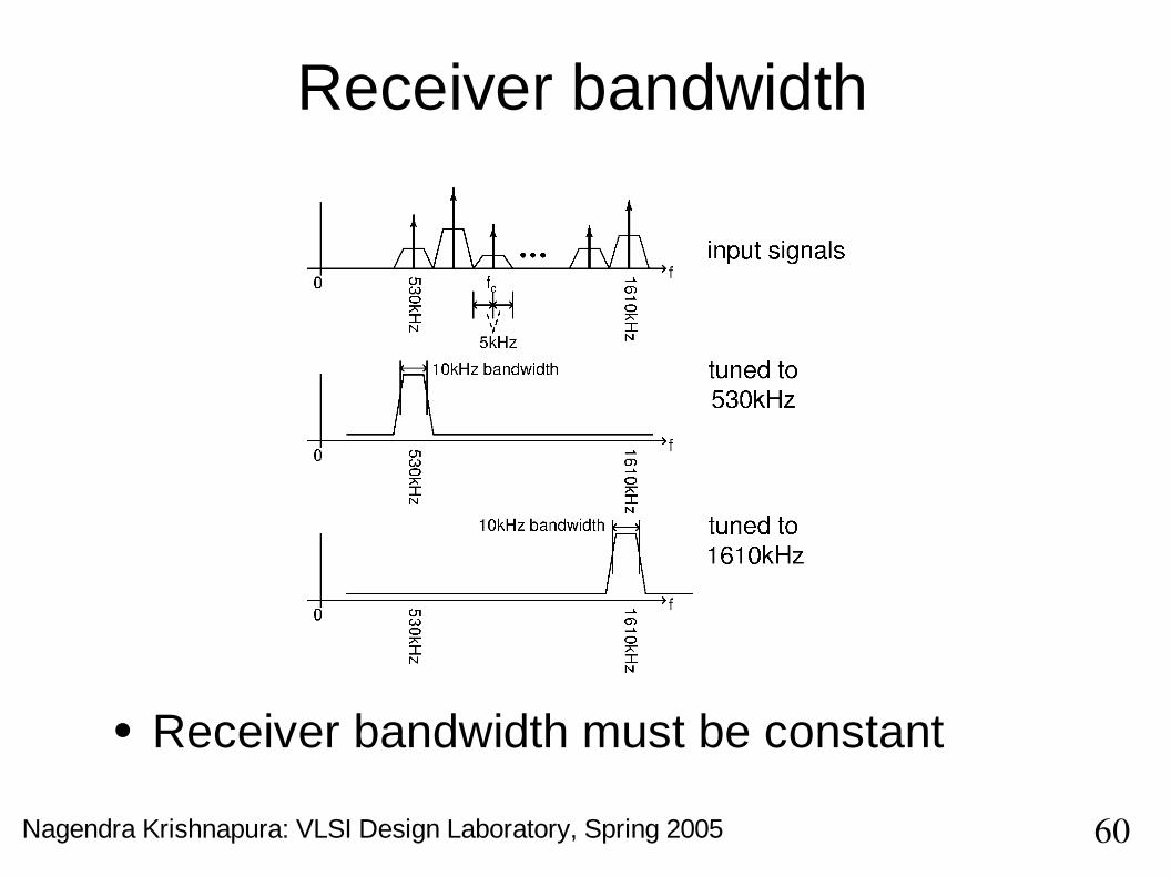
Receiver bandwidth
Receiver bandwidth must be constant
60Nagendra Krishnapura: VLSI Design Laboratory, Spring 2005

Receiver bandwidth
fc/f
bw=53 at the lowest end
fc/f
bw=161 at the highest end
High Q (~ quality factor) Maintain constant bandwidth
61Nagendra Krishnapura: VLSI Design Laboratory, Spring 2005
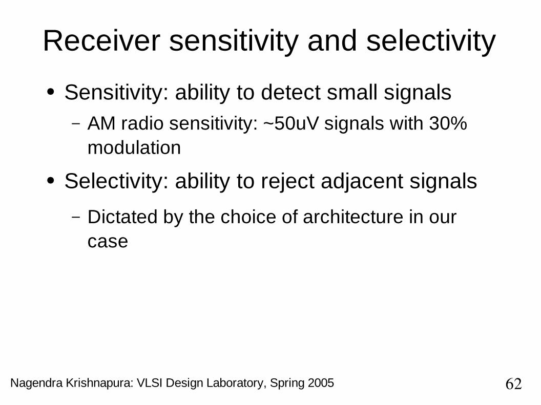
Receiver sensitivity and selectivity
Sensitivity: ability to detect small signals– AM radio sensitivity: ~50uV signals with 30%
modulation
Selectivity: ability to reject adjacent signals
– Dictated by the choice of architecture in our case
62Nagendra Krishnapura: VLSI Design Laboratory, Spring 2005

Tuned Radio Frequency(TRF) receiver
Input tuned circuit is the only filter providing selectivity
Coil on a ferrite rod
63Nagendra Krishnapura: VLSI Design Laboratory, Spring 2005

TRF receiver: input tuning
64Nagendra Krishnapura: VLSI Design Laboratory, Spring 2005

Resonant frequency(radians per second) ωo
= 1/sqrt(LCtune
)
3dB bandwidth ωb
Quality factor Q = ω0/ω
b
Series loss: Qs = 1/R
ssqrt(L/C)
– Bandwidth = Rs/L
Parallel loss: Qp = R
psqrt(C/L)
– Bandwidth = 1/CRp
65Nagendra Krishnapura: VLSI Design Laboratory, Spring 2005
2nd order filter basics

Resonant frequency(1/sqrt(LCtune
)) varies
from 530 to 1610kHz, approx 3x Fixed L, ⇒ C
tune varies by 9x
Series loss(Rs) only
– Bandwidth = Rs/L
– No change with Ctune
Parallel loss(Rp) only
– Bandwidth = 1/Ctune
Rs
– varies by 9x with change in Ctune
66Nagendra Krishnapura: VLSI Design Laboratory, Spring 2005
TRF receiver: input tuning

Some bandwidth variation with tuning– Bandwidth < 10kHz at low end– Bandwidth > 10kHz at high end
2nd order filter. Limited out of band attenuation
⇒ Poor selectivity in a TRF receiver Suggestion: Use a very large on chip R
p to
maintain as high a Q as possible
67Nagendra Krishnapura: VLSI Design Laboratory, Spring 2005
TRF receiver: input tuning

High impedance input necessary– Source follower buffer– Differential amplifier
68Nagendra Krishnapura: VLSI Design Laboratory, Spring 2005
TRF receiver: Input amplifier

Use large resistors for input biasing
69Nagendra Krishnapura: VLSI Design Laboratory, Spring 2005
TRF receiver: Input amplifier

70Nagendra Krishnapura: VLSI Design Laboratory, Spring 2005
TRF receiver: Input amplifier

71Nagendra Krishnapura: VLSI Design Laboratory, Spring 2005
TRF receiver: Detector
No diodes in CMOS process Input amplitude > diode drop Use of an amplifier in feedback to improve
sensitivity

72Nagendra Krishnapura: VLSI Design Laboratory, Spring 2005
AM radio: specifications Signal levels: Input from 50µV to 5mV RF amplifier with AGC Output of RF amplifier with AGC from 50mV
to 200mV– Max. gain = 50mV/50µV = 1000 (60dB)– Min. gain = 200mV/5mV = 40 (32dB)– Total gain variability = 1:25 (28dB)
Detector must work with 50mV-200mV inputs
Audio output max. ~ 1Vpk
into 8Ω speaker
73Nagendra Krishnapura: VLSI Design Laboratory, Spring 2005
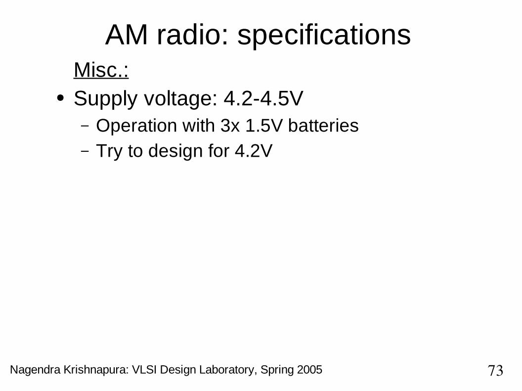
AM radio: specifications Misc.: Supply voltage: 4.2-4.5V
– Operation with 3x 1.5V batteries– Try to design for 4.2V

74Nagendra Krishnapura: VLSI Design Laboratory, Spring 2005
AM radio: input signal generation
Use A from 50µV to 5mV Parameterized subcircuit(using pPar(“m”),
pPar(“A”) etc.) to make an AM source in Cadence
75Nagendra Krishnapura: VLSI Design Laboratory, Spring 2005
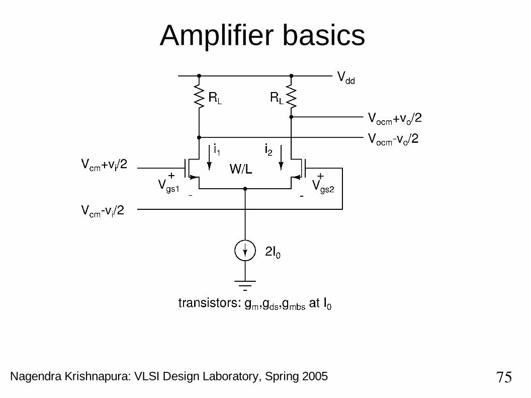
Amplifier basics

76Nagendra Krishnapura: VLSI Design Laboratory, Spring 2005
Gain = gm(R
L+1/g
ds) ~ g
mR
L
Gm = sqrt(µCox
/2*W/L*I0) = I
0/V
GS-V
T
Gain = gmR
L = I
0R
L/V
GS-V
T
– To change gain, I0R
L (the dc voltage drop across
RL) or V
GS-V
T (related to transistor current
density) has to be changed Linearity improves with increasing V
GS-V
T
– Amplifier: larger VGS
-VT
– Switch: smaller VGS
-VT
Amplifier basics

77Nagendra Krishnapura: VLSI Design Laboratory, Spring 2005
RF amplifier I

78Nagendra Krishnapura: VLSI Design Laboratory, Spring 2005
AC coupled to remove offsets Single ended input/output-simple Gain = g
mR
L/2(Analyze this!)
Ac coupling resistors: pMOS transistors Ac coupling corner frequency: ~ 1dB
attenuation at lower end of AM band Capacitor values: 5pF or less
– Linear capacitor density ~ 0.9fF/µm2
Resistor values: upto 10kΩ– Resistivity ~ 800Ω/sq.
RF amplifier I

79Nagendra Krishnapura: VLSI Design Laboratory, Spring 2005
RF amplifier II

80Nagendra Krishnapura: VLSI Design Laboratory, Spring 2005
AC coupled to remove offsets Single ended input/output-simple Gain = g
mR
L(Analyze this!)
Ac coupling resistors: pMOS transistors Ac coupling corner frequency: ~ 1dB
attenuation at lower end of AM band Capacitor values: 5pF or less
– Linear capacitor density ~ 0.9fF/µm2
Resistor values: upto 10kΩ– Resistivity ~ 800Ω/sq.
RF amplifier II

81Nagendra Krishnapura: VLSI Design Laboratory, Spring 2005
RF amplifier III

82Nagendra Krishnapura: VLSI Design Laboratory, Spring 2005
AC coupled to remove offsets Differential stages
– 2x ac coupling capacitors Gain = g
mR
L(Analyze this!)
Ac coupling resistors: pMOS transistors Ac coupling corner frequency: ~ 1dB
attenuation at lower end of AM band Capacitor values: 5pF or less
– Linear capacitor density ~ 0.9fF/µm2
Resistor values: upto 10kΩ– Resistivity ~ 800Ω/sq.
RF amplifier III

83Nagendra Krishnapura: VLSI Design Laboratory, Spring 2005
Detector I

84Nagendra Krishnapura: VLSI Design Laboratory, Spring 2005
Implement vi(t)*sgn(v
i(t)) and filter the result
– Full wave rectification and filtering Filtering capacitor C
– retain audio, remove RF– External, if too large
Upper pair should act as a switch: sgn(vi(t))
Lower pair should act as a linear amplifier(over the entire range of input signals)
Detector I

85Nagendra Krishnapura: VLSI Design Laboratory, Spring 2005
Detector II

86Nagendra Krishnapura: VLSI Design Laboratory, Spring 2005
Full wave rectifier with differential inputs Half wave rectifier with single ended inputs Followed by amplifier and filter Filtering capacitor C
– retain audio, remove RF– External, if too large
Detector II

87Nagendra Krishnapura: VLSI Design Laboratory, Spring 2005
Peak detector
T audio , max ≫RC ≫T RF , min

88Nagendra Krishnapura: VLSI Design Laboratory, Spring 2005
Detector III
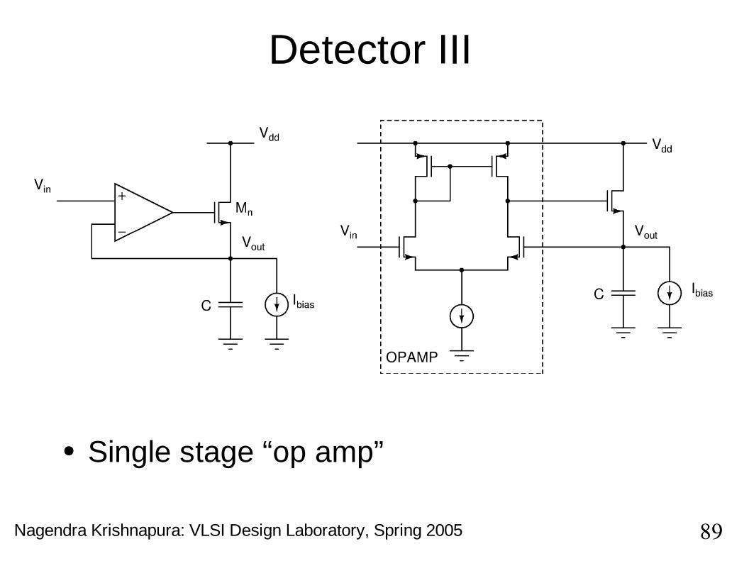
89Nagendra Krishnapura: VLSI Design Laboratory, Spring 2005
Detector III
Single stage “op amp”

90Nagendra Krishnapura: VLSI Design Laboratory, Spring 2005
Peak detector Discharge time constant slower than
charging time constant– Negligible discharge between RF cycles– Full discharge between audio cycles
Detector III

91Nagendra Krishnapura: VLSI Design Laboratory, Spring 2005
Audio amplifier
Feedback for linearity Output current ~ 1V/8Ω = 125mA

92Nagendra Krishnapura: VLSI Design Laboratory, Spring 2005
Class A opamp
Need to bias with I0 = 125mA!

93Nagendra Krishnapura: VLSI Design Laboratory, Spring 2005
Class AB opamp
Vb1
and Vb2
adjusted so that output branch
current is I0

94Nagendra Krishnapura: VLSI Design Laboratory, Spring 2005
Class AB opamp
Output pMOS gate pulled down to drive out a large current ( > bias)

95Nagendra Krishnapura: VLSI Design Laboratory, Spring 2005
Class AB opamp
Output nMOS gate pulled up to pull in a large current (> bias)

96Nagendra Krishnapura: VLSI Design Laboratory, Spring 2005
Class AB opamp: bias generation

97Nagendra Krishnapura: VLSI Design Laboratory, Spring 2005
Class AB opamp: full schematic
98Nagendra Krishnapura: VLSI Design Laboratory, Spring 2005
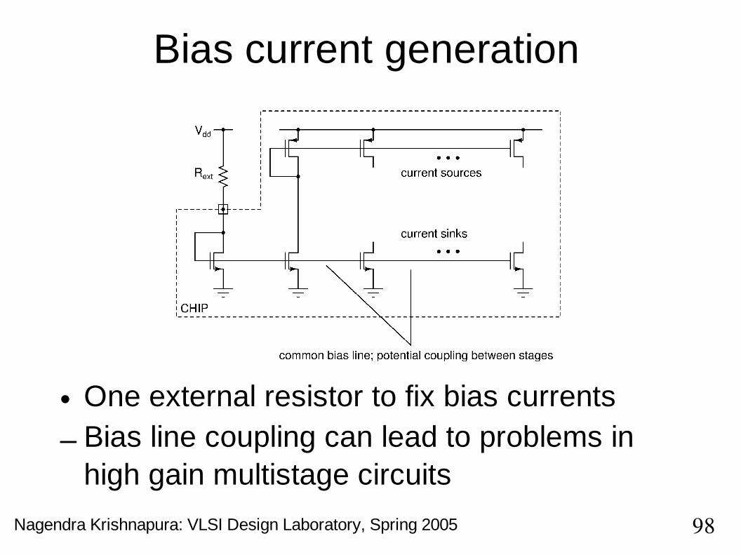
Bias current generation
• One external resistor to fix bias currents
– Bias line coupling can lead to problems in high gain multistage circuits

99Nagendra Krishnapura: VLSI Design Laboratory, Spring 2005
Bias current generation
Separate mirroring branch for each stage
+ Reduced interstage coupling
– Increased current in bias branches

100Nagendra Krishnapura: VLSI Design Laboratory, Spring 2005
Bias current generation
RC filter to each biasing MOS transistor
+ Reduced interference and noise
+ No increase in bias currents

101Nagendra Krishnapura: VLSI Design Laboratory, Spring 2005
Passive components

102Nagendra Krishnapura: VLSI Design Laboratory, Spring 2005
Passive components: Resistors
Passive resistor– Min. width=; few kOhms
MOS resistors– Need bias– Greater range of values– Voltage tunability

103Nagendra Krishnapura: VLSI Design Laboratory, Spring 2005
Passive components: capacitors
Passive (poly1-poly2)– Few pF– Bottom plate to ground parasitic
MOS capacitors– Higher capacitor density– Need to be biased in strong inversion