Embed Size (px)
Citation preview

SPIE Advanced Lithography 2011 paper 7970-1
e-Beam Direct Write of Wafers
1
Aki Fujimura, D2S, Inc

What you do is amazing!Making S-Curves fit a Geometric
2
If you have small S-Curves, you have to stack them one after another
If you are blessed with a big S-Curve, you get to ride it for a long time

“EbDW is always 1-2 generations behind”
3
But that means it HAS kept up with Moore’s Law… Just needs to catch up

Direct-Write or Mask?
Either Way, e-Beam Writes All Chips!
4
GDSII
Write Wafer
Design for
E-beam
(DFEB)
Write Mask
Optimizes design data for
e-beam writing
Contacts/Cuts First
Enables Lower Volume at Leading Nodes
Any Volume
Any Layer

Similar but different…
5
Need Mask Wafer
Size 4x 1x
Accuracy Highest (MEEF) High (less source of error)
Data volume Huge (SRAF) Huge x 10 (no OPC; whole wafer)
Write Time 8-40 hours 1 ~ 100 WPH
Writing Space Rectangle (efficient) Circle (inefficient)
# passes 2, 4 (accuracy) 1 (write time)
Characters Circles 1000’s useful
Market now Solid but flat Zero but big potential
NIL Mask Master is a blend of both

Split Beam Character Proj. General
Multiple Source
Clustering
Source Current
Resist Sensitivity
Regular Design Rules
Borodovsky Method
Other Limits:
Stage
Data Transfer
Calibration
Settling Time …
DFEB = Data Compression DFEB = 10X Speed-up
Maximum flexibility in
shape being written
Maximum transfer of
energy for all shapes
eBeam Speed-Up techniques
6
MSB
Drawing Courtesy of Advantest
SEM Courtesy of e-Shuttle, Inc.

Advantest MCC8Realistic with limited budget is to extend
7
X 10 Cluster

Vistec MSB Hybrid like Prius is the best way to transition
8

IMS, KLA-T REBL, Mapper, MultibeamTake on the bigger S-Curve
9
Multiple beams individually
controlled by various means
Innovation in stage, data pipeline
and column taken as a system
Expensive but worth it

Design to Manufacturing collaborationFocus to succeed : The “Borodovsky method”
10
Design for E-Beam (DFEB)

ASELTA, CEA/Leti, D2S, EQUIcon,
Fraunhofer, Technolution, TSMCSoftware help is essential for this resolution
11
Even eBeam writing is hard at these nodes
• MB-MDP
• MPC
• eRIF
• EBPC
MB-MDP on 80nm L:S for mask
Mapper data prep for 3.5nm resolution

Themes and ApproachesEbDW : we can do this….
• Monetize from the Existing Mask Market
• D2S, IMS, SEMATECH, Vistec
• “Current density advances will not be enough” – Tom Faure, IBM
• EbDW for high volume with clusters
• EbDW can also enable the long tail
• Government funding is deserved
• EbDW will help boost design starts
• That’s good for everyone in the supply chain
12
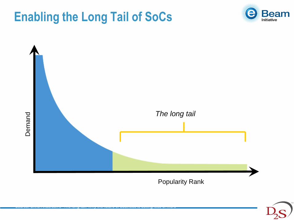
Enabling the Long Tail of SoCs
The long tail
Popularity Rank
Dem
and
Source: Chris Anderson’s “The long tail: Why the future of business is selling less of more”
13

The Tail is Getting Shorter
Cost of Manufacturing
Chips per Design
# of Designs
Re
ve
nu
e p
er
De
sig
n
28-nm with mask
20-nm with mask
14-nm with mask
Maskless SoC
Non-addressable Market
Big opportunity
We can enable the tail with EbDW w/DFEB
More designs
Faster time to market
14

0.1
1.0
10.0
100.0
$100$1,000$10,000$100,000
Reticle ASP
rati
o o
f revis
ed
to
new
desig
ns
>=500-nm
>=300 but <500nm
>=200 but <300nm
>=160 but <200nm
>=120 but <160nm
>=75 but <120nm
Power law fit
Copyright (c) 2007 by VLSI RESEARCH INC. All rights
reserved. Reprinted with permission from VLSI RESEARCH INC.
Derivatives have low design cost10x reduction in mask cost increases derivatives by 10x

Electron Beam Direct Write
• Great for R&D : process, design, systems
• Great for lower-volume : minimal mask cost
• Volume Production? : 50 WPH cluster in 2014
• Please attend these great sessions and learn
about the potential of e-beam technologies
16

17
Session 3: Maskless Lithography I
Date: Tuesday 1 March Time: 1:20 PM - 3:10 PM Session Chairs: Hans Loeschner, IMS Nanofabrication AG (Austria);
Timothy R. Groves, Univ. at Albany
E-beam lithography development, outlook, and critical challenges (Invited Paper) Paper 7970-9 Time: 1:20 PM - 1:50 PM
Author(s): Hans C. Pfeiffer, HCP Consulting Services (United States)
MCC8: throughput enhancement of EB direct writer Paper 7970-10 Time: 1:50 PM - 2:10 PM
Author(s): Hideaki Komami, Masaki Kurokawa, Akio Yamada, Advantest Corp. (Japan)
eMET: 50 keV electron multibeam mask exposure tool Paper 7970-11 Time: 2:10 PM - 2:30 PM
Author(s): Christof Klein, Jan Klikovits, Hans Loeschner, Elmar Platzgummer, IMS Nanofabrication AG (Austria)
Scanning exposures with a MAPPER multibeam system Paper 7970-12 Time: 2:30 PM - 2:50 PM
Author(s): Bert J. Kampherbeek, Christiaan van den Berg, Vincent Kuiper, Niels Vergeer, Stijn Bosschker, Thomas Ooms, Alexandra
Tudorie, Remco J. Jager, MAPPER Lithography (Netherlands); Sjoerd Postma, DEMCON (Netherlands); Guido de Boer, MAPPER
Lithography (Netherlands)
Multishaped beam: development status and update on lithography results Paper 7970-13 Time: 2:50 PM - 3:10 PM
Author(s): Ines A. Stolberg, Matthias Slodowski, Hans-Joachim Doering, Wolfgang H. Dorl, Vistec Electron Beam GmbH (Germany)

18
Model-based mask data preparation and impact on resist heating Paper 7970-37 Time: 5:20 PM - 5:40 PM
Author(s): Aki Fujimura, D2S, Inc. (United States); Takashi Kamikubo, NuFlare Technology, Inc. (Japan); Ingo Bork, D2S, Inc. (United
States
EBDW to complement optical lithography for 1D GDR patterning Paper 7970-36 Time: 5:00 PM - 5:20 PM
Author(s): David K. Lam, David Liu, Multibeam Corp. (United States); Michael C. Smayling, Tela Innovations, Inc. (United States); Ted
Prescop, Multibeam Corp. (United States)
Data path development for massive electron-beam maskless lithography Paper 7970-35 Time: 4:40 PM - 5:00 PM
Author(s): Faruk Krecinic, Jack J. Chen, Shy-Jay Lin, Burn J. Lin, Taiwan Semiconductor Manufacturing Co. Ltd. (Taiwan)
Influence of massively parallel e-beam direct-write pixel size on electron proximity
correction Paper 7970-34 Time: 4:20 PM - 4:40 PM
Author(s): Shy-Jay Lin, Taiwan Semiconductor Manufacturing Co. Ltd. (Taiwan)
IMAGINE: an open consortium to boost maskless lithography take off: first
assessment results on MAPPER technology Paper 7970-33 Time: 4:00 PM - 4:20 PM
Author(s): Laurent Pain, Serge V. Tedesco, Beatrice Icard, Mickael Martin, Christophe Constancias, Lab. d'Electronique de
Technologie de l'Information (France); Bert J. Kampherbeek, MAPPER Lithography (Netherlands)
Fast mask writer: technology options and considerations (Invited Paper) Paper 7970-32 Time: 3:30 PM - 4:00 PM
Author(s): Lloyd C. Litt, SEMATECH Inc. (United States); Timothy R. Groves, Univ. at Albany (United States); Gregory P. Hughes,
SEMATECH, Inc. (United States)
Session 8: Maskless Lithography II
Date: Wednesday 2 March Time: 3:30 PM - 5:40 PM Session Chairs: Lloyd C. Litt, SEMATECH Inc.; Laurent Pain, CEA-LETI (France)

19
New advances with REBL for maskless high-throughput EBDW
lithography (Invited Paper) Paper 7970-43 Time: 10:20 AM - 10:50 AM
Author(s): Paul Petric, Chris Bevis, Mark A. McCord, Allen Carroll, Alan D. Brodie, Upendra Ummethala, Luca
Grella, Regina Freed, KLA-Tencor Corp. (United States)
Large-scale eRIF implementation for sub-22-nm e-beam lithography Paper 7970-44 Time: 10:50 AM - 11:10 AM
Author(s): Luc Martin, Lab. d'Electronique de Technologie de l'Information (France); Serdar Manakli, Sébastien
Bayle, ASELTA Nanographics (France); Kang-Hoon Choi, Manuela S. Gutsch, Fraunhofer-Ctr. Nanoelektronische
Technologien (Germany); Laurent Pain, Lab. d'Electronique de Technologie de l'Information (France)
Demonstration of real-time pattern correction for high-throughput
maskless lithography Paper 7970-45 Time: 11:10 AM - 11:30 AM
Author(s): Marco J. Wieland, Ton van de Peut, Martijn Sanderse, MAPPER Lithography (Netherlands); Edwin
Hakkennes, Nol Venema, Ard Wiersma, Mark Hoving, Sijmen Woutersen, Technolution B.V. (Netherlands)
EBPC for multibeams low-kV electron projection lithography Paper 7970-46 Time: 11:30 AM - 11:50 AM
Author(s): Jérôme Belledent, Sebastien Soulan, Laurent Pain, Commissariat à l'Énergie Atomique (France)
Fast characterization of line-end shortening and application of novel LES
correction algorithms in e-beam direct write Paper 7970-47 Time: 11:50 AM - 12:10 PM
Author(s): Martin Freitag, Manuela S. Gutsch, Kang-Hoon Choi, Christoph K. Hohle, Fraunhofer-Ctr.
Nanoelektronische Technologien (Germany); Michael Krüger, EQUIcon Software GmbH Jena (Germany); Ulf
Weidenmüller, Vistec Electron Beam GmbH (Germany)
Session 10: Maskless Lithography III
Date: Thursday 3 March Time: 10:20 AM - 12:10 PM Session Chairs: Lloyd C. Litt, SEMATECH Inc.; Hans Loeschner, IMS Nanofabrication AG (Austria)

It’s time to make it happen…
• EbDW will scale, once it catches a node
• Need to collaborate and coordinate even more
• Too many teams in the league is diluting the quality and funding
• Column, stage, data-path and integration should share
• EbDW projects need more funding
• Will help boost design starts at the leading edge nodes
• Good for everyone in the supply chain
• Spurs more silicon innovation
• Fuels more systems innovation
20