Embed Size (px)
Citation preview

© 2010 Microchip Technology Inc. DS70135G
dsPIC30F4011/4012Data Sheet
High-Performance,16-Bit Digital Signal Controllers

Note the following details of the code protection feature on Microchip devices:• Microchip products meet the specification contained in their particular Microchip Data Sheet.
• Microchip believes that its family of products is one of the most secure families of its kind on the market today, when used in the intended manner and under normal conditions.
• There are dishonest and possibly illegal methods used to breach the code protection feature. All of these methods, to our knowledge, require using the Microchip products in a manner outside the operating specifications contained in Microchip’s Data Sheets. Most likely, the person doing so is engaged in theft of intellectual property.
• Microchip is willing to work with the customer who is concerned about the integrity of their code.
• Neither Microchip nor any other semiconductor manufacturer can guarantee the security of their code. Code protection does not mean that we are guaranteeing the product as “unbreakable.”
Code protection is constantly evolving. We at Microchip are committed to continuously improving the code protection features of ourproducts. Attempts to break Microchip’s code protection feature may be a violation of the Digital Millennium Copyright Act. If such actsallow unauthorized access to your software or other copyrighted work, you may have a right to sue for relief under that Act.
Information contained in this publication regarding deviceapplications and the like is provided only for your convenienceand may be superseded by updates. It is your responsibility toensure that your application meets with your specifications.MICROCHIP MAKES NO REPRESENTATIONS ORWARRANTIES OF ANY KIND WHETHER EXPRESS ORIMPLIED, WRITTEN OR ORAL, STATUTORY OROTHERWISE, RELATED TO THE INFORMATION,INCLUDING BUT NOT LIMITED TO ITS CONDITION,QUALITY, PERFORMANCE, MERCHANTABILITY ORFITNESS FOR PURPOSE. Microchip disclaims all liabilityarising from this information and its use. Use of Microchipdevices in life support and/or safety applications is entirely atthe buyer’s risk, and the buyer agrees to defend, indemnify andhold harmless Microchip from any and all damages, claims,suits, or expenses resulting from such use. No licenses areconveyed, implicitly or otherwise, under any Microchipintellectual property rights.
DS70135G-page 2
Trademarks
The Microchip name and logo, the Microchip logo, dsPIC, KEELOQ, KEELOQ logo, MPLAB, PIC, PICmicro, PICSTART, PIC32 logo, rfPIC and UNI/O are registered trademarks of Microchip Technology Incorporated in the U.S.A. and other countries.
FilterLab, Hampshire, HI-TECH C, Linear Active Thermistor, MXDEV, MXLAB, SEEVAL and The Embedded Control Solutions Company are registered trademarks of Microchip Technology Incorporated in the U.S.A.
Analog-for-the-Digital Age, Application Maestro, CodeGuard, dsPICDEM, dsPICDEM.net, dsPICworks, dsSPEAK, ECAN, ECONOMONITOR, FanSense, HI-TIDE, In-Circuit Serial Programming, ICSP, Mindi, MiWi, MPASM, MPLAB Certified logo, MPLIB, MPLINK, mTouch, Omniscient Code Generation, PICC, PICC-18, PICDEM, PICDEM.net, PICkit, PICtail, REAL ICE, rfLAB, Select Mode, Total Endurance, TSHARC, UniWinDriver, WiperLock and ZENA are trademarks of Microchip Technology Incorporated in the U.S.A. and other countries.
SQTP is a service mark of Microchip Technology Incorporated in the U.S.A.
All other trademarks mentioned herein are property of their respective companies.
© 2010, Microchip Technology Incorporated, Printed in the U.S.A., All Rights Reserved.
Printed on recycled paper.
ISBN: 978-1-60932-713-2Microchip received ISO/TS-16949:2002 certification for its worldwide
© 2010 Microchip Technology Inc.
headquarters, design and wafer fabrication facilities in Chandler and Tempe, Arizona; Gresham, Oregon and design centers in California and India. The Company’s quality system processes and procedures are for its PIC® MCUs and dsPIC® DSCs, KEELOQ® code hopping devices, Serial EEPROMs, microperipherals, nonvolatile memory and analog products. In addition, Microchip’s quality system for the design and manufacture of development systems is ISO 9001:2000 certified.

dsPIC30F4011/4012High-Performance, 16-Bit Digital Signal Controllers
High-Performance, Modified RISC CPU:• Modified Harvard architecture• C compiler optimized instruction set architecture
with flexible addressing modes• 83 base instructions• 24-bit wide instructions, 16-bit wide data path• 48 Kbytes on-chip Flash program space
(16K instruction words)• 2 Kbytes of on-chip data RAM• 1 Kbyte of nonvolatile data EEPROM• Up to 30 MIPS operation:
- DC to 40 MHz external clock input- 4 MHz-10 MHz oscillator input with
PLL active (4x, 8x, 16x)• 30 interrupt sources:
- Three external interrupt sources- Eight user-selectable priority levels for each
interrupt source- Four processor trap sources
• 16 x 16-bit working register array
DSP Engine Features:• Dual data fetch• Accumulator write-back for DSP operations • Modulo and Bit-Reversed Addressing modes• Two, 40-bit wide accumulators with optional
saturation logic• 17-bit x 17-bit single-cycle hardware
fractional/integer multiplier• All DSP instructions are single cycle• ±16-bit, single-cycle shift
Peripheral Features:• High-current sink/source I/O pins: 25 mA/25 mA• Timer module with programmable prescaler:
- Five 16-bit timers/counters; optionally pair 16-bit timers into 32-bit timer modules
• 16-bit Capture input functions• 16-bit Compare/PWM output functions• 3-wire SPI modules (supports 4 Frame modes)• I2C™ module supports Multi-Master/Slave mode
and 7-bit/10-bit addressing• Two UART modules with FIFO Buffers• CAN module, 2.0B compliant
Motor Control PWM Module Features:• Six PWM output channels:
- Complementary or Independent Output modes
- Edge and Center-Aligned modes• Three duty cycle generators • Dedicated time base• Programmable output polarity• Dead-time control for Complementary mode• Manual output control• Trigger for A/D conversions
Quadrature Encoder Interface Module Features:• Phase A, Phase B and Index Pulse input• 16-bit up/down position counter • Count direction status• Position Measurement (x2 and x4) mode• Programmable digital noise filters on inputs• Alternate 16-bit Timer/Counter mode• Interrupt on position counter rollover/underflow
Analog Features:• 10-bit Analog-to-Digital Converter (ADC) with
four Sample and Holde (S&H) inputs:- 1 Msps conversion rate- Nine input channels- Conversion available during Sleep and Idle
• Programmable Brown-out Reset
Note: This data sheet summarizes features ofthis group of dsPIC30F devices and is notintended to be a complete referencesource. For more information on the CPU,peripherals, register descriptions andgeneral device functionality, refer to the“dsPIC30F Family Reference Manual”(DS70046). For more information on thedevice instruction set and programming,refer to the “16-bit MCU and DSCReference Manual” (DS70157).
© 2010 Microchip Technology Inc. DS70135G-page 3
dsPIC30F4011/4012
Special Digital Signal Controller Features:• Enhanced Flash program memory:- 10,000 erase/write cycle (min.) for industrial temperature range, 100K (typical)
• Data EEPROM memory:- 100,000 erase/write cycle (min.) for
industrial temperature range, 1M (typical)• Self-reprogrammable under software control• Power-on Reset (POR), Power-up Timer (PWRT)
and Oscillator Start-up Timer (OST)• Flexible Watchdog Timer (WDT) with on-chip,
low-power RC oscillator for reliable operation• Fail-Safe Clock Monitor operation detects clock
failure and switches to on-chip, low-power RC oscillator
• Programmable code protection• In-Circuit Serial Programming™ (ICSP™)• Selectable Power Management modes:
- Sleep, Idle and Alternate Clock modes
CMOS Technology:• Low-power, high-speed Flash technology• Wide operating voltage range (2.5V to 5.5V)• Industrial and Extended temperature ranges• Low-power consumption
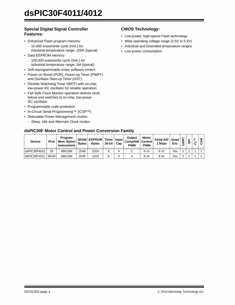
dsPIC30F Motor Control and Power Conversion Family
Device PinsProgram
Mem. Bytes/Instructions
SRAMBytes
EEPROMBytes
Timer 16-bit
InputCap
OutputComp/Std
PWM
MotorControl
PWM
10-bit A/D 1 Msps
Quad Enc U
AR
T
SPI
I2 C™
CA
N
dsPIC30F4012 28 48K/16K 2048 1024 5 4 2 6 ch 6 ch Yes 1 1 1 1dsPIC30F4011 40/44 48K/16K 2048 1024 5 4 4 6 ch 9 ch Yes 2 1 1 1
DS70135G-page 4 © 2010 Microchip Technology Inc.

dsPIC30F4011/4012
Pin DiagramsAN7/RB7AN6/OCFA/RB6
C1RX/RF0C1TX/RF1
OC3/RD2EMUC2/OC1/IC1/INT1/RD0
AN8/RB8
1234567891011121314151617181920
4039383736353433323130292827262524232221
dsPIC30F4011
MCLR
VDDVSS
EMUD2/OC2/IC2/INT2/RD1
EMUC1/SOSCO/T1CK/U1ARX/CN0/RC14EMUD1/SOSCI/T2CK/U1ATX/CN1/RC13
OSC2/CLKO/RC15OSC1/CLKI
PWM1L/RE0PWM1H/RE1PWM2L/RE2PWM2H/RE3
PWM3H/RE5
AVDDAVSS
OC4/RD3
VSSVDD
SCK1/RF6
PGC/EMUC/U1RX/SDI1/SDA/RF2PGD/EMUD/U1TX/SDO1/SCL/RF3
PWM3L/RE4
VDD
U2RX/CN17/RF4U2TX/CN18/RF5
AN4/QEA/IC7/CN6/RB4
AN2/SS1/CN4/RB2EMUC3/AN1/VREF-/CN3/RB1EMUD3/AN0/VREF+/CN2/RB0
AN5/QEB/IC8/CN7/RB5
FLTA/INT0/RE8
VSS
AN3/INDX/CN5/RB3
40-Pin PDIP
1011
23456
1
18 19 20 21 2212 13 14 15
38
87
44 43 42 41 40 3916 17
2930313233
232425262728
36 3435
9
37
PG
D/E
MU
D/U
1TX/
SDO
1/S
CL/
RF3
SC
K1/
RF6
EM
UC
2/O
C1/
IC1/
INT1
/RD
0O
C3/
RD
2V
DD
EM
UC
1/SO
SC
O/T
1CK/
U1A
RX
/CN
0/R
C14
NC
VS
SO
C4/
RD
3E
MU
D2/
OC
2/IC
2/IN
T2/R
D1
FLTA
/INT0
/RE
8
AN
3/IN
DX
/CN
5/R
B3
AN2/
SS1/
CN
4/R
B2
EM
UC
3/A
N1/
V RE
F-/C
N3/
RB
1E
MU
D3/
AN
0/V R
EF+
/CN
2/R
B0
MC
LRNC
AVD
DAV
SS
PW
M1L
/RE
0P
WM
1H/R
E1
PWM2H/RE3PWM3L/RE4PWM3H/RE5
VDDVSS
C1RX/RF0C1TX/RF1
U2RX/CN17/RF4U2TX/CN18/RF5
PGC/EMUC/U1RX/SDI1/SDA/RF2
AN4/QEA/IC7/CN6/RB4AN5/QEB/IC8/CN7/RB5AN6/OCFA/RB6AN7/RB7AN8/RB8
NC
VDDVSSOSC1/CLKIOSC2/CLKO/RC15EMUD1/SOSCI/T2CK/U1ATX/CN1/RC13
44-Pin TQFP
dsPIC30F4011
PWM2L/RE2
NC
© 2010 Microchip Technology Inc. DS70135G-page 5
dsPIC30F4011/4012
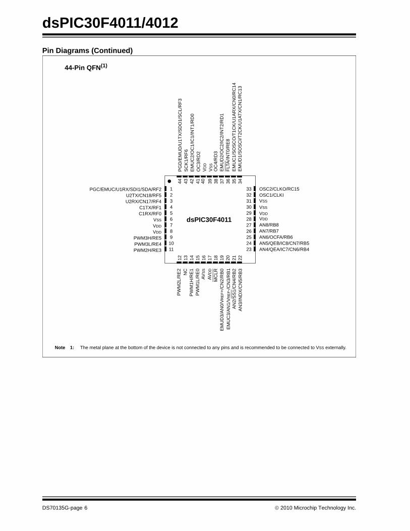
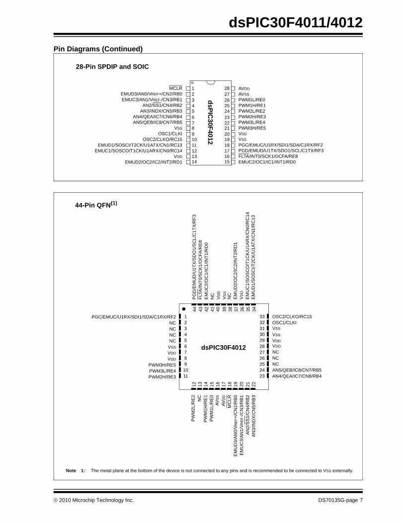
Pin Diagrams (Continued)44-Pin QFN(1)
44 43 42 41 40 39 38 37 36 35
14 15 16 17 18 19 20 21
33029282726252423
45
789
1011
12 32
31
dsPIC30F4011
PWM2H/RE3PWM3L/RE4PWM3H/RE5
VDDVDD
C1RX/RF0C1TX/RF1
U2RX/CN17/RF4U2TX/CN18/RF5
PGC/EMUC/U1RX/SDI1/SDA/RF2
AN3/
IND
X/C
N5/
RB3
AN
2/S
S1/C
N4/
RB2
EMU
C3/
AN1/
VRE
F-/C
N3/
RB
1E
MU
D3/
AN
0/V R
EF+
/CN
2/R
B0M
CLR
AVD
D
PW
M1L
/RE0
PWM
1H/R
E1
PW
M2L
/RE2
AN4/QEA/IC7/CN6/RB4AN5/QEB/IC8/CN7/RB5AN6/OCFA/RB6AN7/RB7AN8/RB8
VDDVSS
OSC1/CLKIOSC2/CLKO/RC15
PG
D/E
MU
D/U
1TX
/SD
O1/
SC
L/R
F3S
CK
1/R
F6E
MU
C2/
OC
1/IC
1/IN
T1/R
D0
OC
3/R
D2
VD
D
EM
UC
1/SO
SC
O/T
1CK/
U1A
RX
/CN
0/R
C14
OC
4/R
D3
EM
UD
2/O
C2/
IC2/
INT2
/RD
1FL
TA/IN
T0/R
E8
6
22
33
34
VSS
AVS
S
VDD
VS
S
EM
UD
1/SO
SC
I/T2C
K/U
1ATX
/CN
1/R
C13
VSS
NC
12 13
Note 1: The metal plane at the bottom of the device is not connected to any pins and is recommended to be connected to VSS externally.
DS70135G-page 6 © 2010 Microchip Technology Inc.
dsPIC30F4011/4012
Pin Diagrams (Continued)dsPIC30F4012
MCLR
PWM1L/RE0PWM1H/RE1PWM2L/RE2PWM2H/RE3PWM3L/RE4PWM3H/RE5VSS
VDD
EMUD3/AN0/VREF+/CN2/RB0EMUC3/AN1/VREF-/CN3/RB1
AVDDAVSS
AN2/SS1/CN4/RB2
EMUD2/OC2/IC2/INT2/RD1 EMUC2/OC1/IC1/INT1/RD0
EMUC1/SOSCO/T1CK/U1ARX/CN0/RC14EMUD1/SOSCI/T2CK/U1ATX/CN1/RC13
VSSOSC2/CLKO/RC15OSC1/CLKI VDD
FLTA/INT0/SCK1/OCFA/RE8
PGC/EMUC/U1RX/SDI1/SDA/C1RX/RF2PGD/EMUD/U1TX/SDO1/SCL/C1TX/RF3
AN5/QEB/IC8/CN7/RB5AN4/QEA/IC7/CN6/RB4
AN3/INDX/CN5/RB3
1234567891011121314
2827262524232221201918171615
28-Pin SPDIP and SOIC
44-Pin QFN(1)
33029282726252423
45
789
1011
12 32
31
dsPIC30F4012
PWM2H/RE3PWM3L/RE4PWM3H/RE5
VDDVDD
NCNCNCNC
PGC/EMUC/U1RX/SDI1/SDA/C1RX/RF2
AN3/
IND
X/C
N5/
RB3
AN2/
SS1 /
CN
4/R
B2E
MU
C3/
AN
1/VR
EF-
/CN
3/R
B1E
MU
D3/
AN
0/V R
EF+
/CN
2/R
B0M
CLR
AVD
D
PW
M1L
/RE0
PWM
1H/R
E1
PW
M2L
/RE2
AN4/QEA/IC7/CN6/RB4AN5/QEB/IC8/CN7/RB5NCNCNC
VDDVSS
OSC1/CLKIOSC2/CLKO/RC15
PG
D/E
MU
D/U
1TX
/SD
O1/
SCL/
C1T
X/R
F3FL
TA/IN
T0/S
CK1
/OC
FA/R
E8
EM
UC
2/O
C1/
IC1/
INT1
/RD
0N
CV
DD
EM
UC
1/S
OSC
O/T
1CK
/U1A
RX
/CN
0/R
C14
NC
EM
UD
2/O
C2/
IC2/
INT2
/RD
1V
DD
6
33
VSS
AVS
S
VDD
VS
S
EM
UD
1/S
OSC
I/T2C
K/U
1ATX
/CN
1/R
C13
VSS
NC
14 15 16 17 18 19 20 21 2212 1344 43 42 41 40 39 38 37 36 35 34
Note 1: The metal plane at the bottom of the device is not connected to any pins and is recommended to be connected to VSS externally.
© 2010 Microchip Technology Inc. DS70135G-page 7

dsPIC30F4011/4012
Table of Contents1.0 Device Overview .......................................................................................................................................................................... 92.0 CPU Architecture Overview........................................................................................................................................................ 173.0 Memory Organization ................................................................................................................................................................. 254.0 Address Generator Units............................................................................................................................................................ 375.0 Interrupts .................................................................................................................................................................................... 436.0 Flash Program Memory.............................................................................................................................................................. 497.0 Data EEPROM Memory ............................................................................................................................................................. 558.0 I/O Ports ..................................................................................................................................................................................... 619.0 Timer1 Module ........................................................................................................................................................................... 6710.0 Timer2/3 Module ........................................................................................................................................................................ 7111.0 Timer4/5 Module ....................................................................................................................................................................... 7712.0 Input Capture Module................................................................................................................................................................. 8113.0 Output Compare Module ............................................................................................................................................................ 8514.0 Quadrature Encoder Interface (QEI) Module ............................................................................................................................. 9115.0 Motor Control PWM Module ....................................................................................................................................................... 9716.0 SPI™ Module ........................................................................................................................................................................... 10917.0 I2C™ Module ........................................................................................................................................................................... 11318.0 Universal Asynchronous Receiver Transmitter (UART) Module .............................................................................................. 12119.0 CAN Module ............................................................................................................................................................................. 12920.0 10-bit, High-Speed Analog-to-Digital Converter (ADC) Module ............................................................................................... 13921.0 System Integration ................................................................................................................................................................... 15122.0 Instruction Set Summary .......................................................................................................................................................... 16523.0 Development Support............................................................................................................................................................... 17324.0 Electrical Characteristics .......................................................................................................................................................... 17725.0 Packaging Information.............................................................................................................................................................. 219The Microchip Web Site ..................................................................................................................................................................... 235Customer Change Notification Service .............................................................................................................................................. 235Customer Support .............................................................................................................................................................................. 235Reader Response .............................................................................................................................................................................. 236Product Identification System............................................................................................................................................................. 237TO OUR VALUED CUSTOMERSIt is our intention to provide our valued customers with the best documentation possible to ensure successful use of your Microchipproducts. To this end, we will continue to improve our publications to better suit your needs. Our publications will be refined andenhanced as new volumes and updates are introduced. If you have any questions or comments regarding this publication, please contact the Marketing Communications Department viaE-mail at [email protected] or fax the Reader Response Form in the back of this data sheet to (480) 792-4150. Wewelcome your feedback.
Most Current Data SheetTo obtain the most up-to-date version of this data sheet, please register at our Worldwide Web site at:
http://www.microchip.comYou can determine the version of a data sheet by examining its literature number found on the bottom outside corner of any page.The last character of the literature number is the version number, (e.g., DS30000A is version A of document DS30000).
ErrataAn errata sheet, describing minor operational differences from the data sheet and recommended workarounds, may exist for currentdevices. As device/documentation issues become known to us, we will publish an errata sheet. The errata will specify the revision ofsilicon and revision of document to which it applies.To determine if an errata sheet exists for a particular device, please check with one of the following:• Microchip’s Worldwide Web site; http://www.microchip.com• Your local Microchip sales office (see last page)When contacting a sales office, please specify which device, revision of silicon and data sheet (include literature number) you areusing.
Customer Notification SystemRegister on our web site at www.microchip.com to receive the most current information on all of our products.
DS70135G-page 8 © 2010 Microchip Technology Inc.

dsPIC30F4011/4012
1.0 DEVICE OVERVIEWThis document contains device-specific information forthe dsPIC30F4011/4012 devices. The dsPIC30Fdevices contain extensive Digital Signal Processor(DSP) functionality within a high-performance, 16-bitmicrocontroller (MCU) architecture. Figure 1-1 andFigure 1-2 illustrate device block diagrams for thedsPIC30F4011 and dsPIC30F4012 devices.
Note: This data sheet summarizes features ofthis group of dsPIC30F devices and is notintended to be a complete referencesource. For more information on the CPU,peripherals, register descriptions andgeneral device functionality, refer to the“dsPIC30F Family Reference Manual”(DS70046). For more information on thedevice instruction set and programming,refer to the “16-bit MCU and DSCProgrammer’s Reference Manual”(DS70157).
© 2010 Microchip Technology Inc. DS70135G-page 9

dsPIC30F4011/4012
FIGURE 1-1: dsPIC30F4011 BLOCK DIAGRAMAN8/RB8
Power-upTimer
OscillatorStart-up Timer
POR/BORReset
WatchdogTimer
InstructionDecode and
Control
OSC1/CLKI
MCLR
VDD, VSS
AN4/QEA/IC7/CN6/RB4
UART1,SPI1 Motor ControlPWM
TimingGeneration
CAN
AN5/QEB/IC8/CN7/RB5
16
PCH PCLProgram Counter
ALU<16>
16
Address Latch
Program Memory(48 Kbytes)
Data Latch
24
24
24
24
X Data Bus
IR
I2C™
QEI
AN6/OCFA/RB6AN7/RB7
PCU
PWM1L/RE0PWM1H/RE1PWM2L/RE2PWM2H/RE3PWM3L/RE4
10-bit ADC
TimersPWM3H/RE5FLTA/INT0/RE8
U2TX/CN18/RF5SCK1/RF6
InputCaptureModule
Output Compare
Module
EMUC1/SOSCO/T1CK/U1ARX/CN0/RC14EMUD1/SOSCI/T2CK/U1ATX/CN1/RC13
PORTB
C1RX/RF0C1TX/RF1PGC/EMUC/U1RX/SDI1/SDA/RF2PGD/EMUD/U1TX/SDO1/SCL/RF3
PORTF
PORTD
16
16 16
16 x 16W Reg Array
Divide UnitEngine
DSP
Decode
ROM Latch
16
Y Data Bus
Effective Address
X RAGUX WAGUY AGU
EMUD3/AN0/VREF+/CN2/RB0EMUC3/AN1/VREF-/CN3/RB1AN2/SS1/CN4/RB2AN3/INDX/CN5/RB3
OSC2/CLKO/RC15
U2RX/CN17/RF4
AVDD, AVSS
UART2
16
16
16
16
16
PORTC
PORTE
16
16
16
16
8
InterruptController PSV & Table
Data AccessControl Block
StackControlLogic
LoopControlLogic
Data LatchData LatchY Data
(1 Kbyte)RAM
X Data
(1 Kbyte)RAM
AddressLatch
AddressLatch
Control Signals to Various
EMUC2/OC1/IC1/INT1/RD0EMUD2/OC2/IC2/INT2/RD1OC3/RD2OC4/RD3
16
Data EEPROM(1 Kbyte)
16
Blocks
DS70135G-page 10 © 2010 Microchip Technology Inc.

dsPIC30F4011/4012
FIGURE 1-2: dsPIC30F4012 BLOCK DIAGRAMPower-upTimer
OscillatorStart-up Timer
POR/BORReset
WatchdogTimer
InstructionDecode and
Control
OSC1/CLKI
MCLR
VDD, VSS
AN4/QEA/IC7/CN6/RB4
UART1,SPI1, Motor ControlPWM
TimingGeneration
CAN
AN5/QEB/IC8/CN7/RB5
16
PCH PCLProgram Counter
ALU<16>
16
Address Latch
Program Memory(48 Kbytes)
Data Latch
24
24
24
24
X Data Bus
IR
I2C™
QEI
PCU
PWM1L/RE0PWM1H/RE1PWM2L/RE2PWM2H/RE3PWM3L/RE4
10-bit ADC
TimersPWM3H/RE5FLTA/INT0/SCK1/OCFA/RE8
InputCaptureModule
Output Compare
Module
EMUC1/SOSCO/T1CK/U1ARX/CN0/RC14EMUD1/SOSCI/T2CK/U1ATX/CN1/RC13
PORTB
PGC/EMUC/U1RX/SDI1/SDA/C1RX/RF2PGD/EMUD/U1TX/SDO1/SCL/C1TX/RF3
PORTF
PORTD
16
16 16
16 x 16W Reg Array
Divide Unit Engine
DSP
Decode
ROM Latch
16
Y Data Bus
Effective Address
X RAGUX WAGU Y AGU
EMUD3/AN0/VREF+/CN2/RB0EMUC3/AN1/VREF-/CN3/RB1AN2/SS1/CN4/RB2AN3/INDX/CN5/RB3
OSC2/CLKO/RC15
AVDD, AVSS
UART2
16
16
16
16
16
PORTC
PORTE
16
16
16
16
8
InterruptController PSV & Table
Data AccessControl Block
StackControl Logic
LoopControlLogic
Data LatchData LatchY Data
(1 Kbyte)RAM
X Data
(1 Kbyte)RAM
AddressLatch
AddressLatch
Control Signals to Various
EMUC2/OC1/IC1/INT1RD0EMUD2/OC2/IC2/INT2/RD1
16
Data EEPROM(1 Kbyte)
16
SPI2
Blocks
© 2010 Microchip Technology Inc. DS70135G-page 11

dsPIC30F4011/4012
Table 1-1 provides a brief description of the device I/Opinout and the functions that are multiplexed to a portpin. Multiple functions may exist on one port pin. Whenmultiplexing occurs, the peripheral module’s functionalrequirements may force an override of the datadirection of the port pin.TABLE 1-1: dsPIC30F4011 I/O PIN DESCRIPTIONS
Pin Name Pin Type
Buffer Type Description
AN0-AN8 I Analog Analog input channels. AN0 and AN1 are also used for device programming data and clock inputs, respectively.
AVDD P P Positive supply for analog module. This pin must be connected at all times.AVSS P P Ground reference for analog module. This pin must be connected at all times.CLKICLKO
IO
ST/CMOS—
External clock source input. Always associated with OSC1 pin function.Oscillator crystal output. Connects to crystal or resonator in Crystal Oscillator mode. Optionally functions as CLKO in RC and EC modes.Always associated with OSC2 pin function.
CN0-CN7CN17-CN18
I ST Input change notification inputs. Can be software programmed for internal weak pull-ups on all inputs.
C1RXC1TX
IO
ST—
CAN1 bus receive pin.CAN1 bus transmit pin.
EMUDEMUCEMUD1EMUC1EMUD2EMUC2EMUD3EMUC3
I/OI/OI/OI/OI/OI/OI/OI/O
STSTSTSTSTSTSTST
ICD Primary Communication Channel data input/output pin.ICD Primary Communication Channel clock input/output pin.ICD Secondary Communication Channel data input/output pin.ICD Secondary Communication Channel clock input/output pin.ICD Tertiary Communication Channel data input/output pin.ICD Tertiary Communication Channel clock input/output pin.ICD Quaternary Communication Channel data input/output pin.ICD Quaternary Communication Channel clock input/output pin.
IC1, IC2, IC7, IC8
I ST Capture inputs 1, 2, 7 and 8.
INDXQEA
QEB
II
I
STST
ST
Quadrature Encoder Index Pulse input.Quadrature Encoder Phase A input in QEI mode. Auxiliary Timer External Clock/Gate input in Timer mode.Quadrature Encoder Phase B input in QEI mode. Auxiliary Timer External Clock/Gate input in Timer mode.
INT0INT1INT2
III
STSTST
External interrupt 0.External interrupt 1.External interrupt 2.
FLTAPWM1LPWM1HPWM2LPWM2HPWM3LPWM3H
IOOOOOO
ST——————
PWM Fault A input.PWM1 low output. PWM1 high output.PWM2 low output.PWM2 high output.PWM3 low output.PWM3 high output.
MCLR I/P ST Master Clear (Reset) input or programming voltage input. This pin is an active-low Reset to the device.
OCFAOC1-OC4
IO
ST—
Compare Fault A input (for Compare channels 1, 2, 3 and 4).Compare outputs 1 through 4.
Legend: CMOS = CMOS compatible input or output Analog = Analog inputST = Schmitt Trigger input with CMOS levels O = Output I = Input P = Power
DS70135G-page 12 © 2010 Microchip Technology Inc.

dsPIC30F4011/4012
OSC1
OSC2
I
I/O
ST/CMOS
—
Oscillator crystal input. ST buffer when configured in RC mode; CMOS otherwise.Oscillator crystal output. Connects to crystal or resonator in Crystal Oscillator mode. Optionally functions as CLKO in RC and EC modes.
PGDPGC
I/OI
STST
In-Circuit Serial Programming™ data input/output pin.In-Circuit Serial Programming clock input pin.
RB0-RB8 I/O ST PORTB is a bidirectional I/O port.RC13-RC15 I/O ST PORTC is a bidirectional I/O port.RD0-RD3 I/O ST PORTD is a bidirectional I/O port.RE0-RE5, RE8
I/O ST PORTE is a bidirectional I/O port.
RF0-RF6 I/O ST PORTF is a bidirectional I/O port.SCK1SDI1SDO1SS1
I/OIOI
STST—ST
Synchronous serial clock input/output for SPI1.SPI1 data in.SPI1 data out.SPI1 slave synchronization.
SCLSDA
I/OI/O
STST
Synchronous serial clock input/output for I2C™.Synchronous serial data input/output for I2C.
SOSCOSOSCI
OI
—ST/CMOS
32 kHz low-power oscillator crystal output. 32 kHz low-power oscillator crystal input. ST buffer when configured in RC mode; CMOS otherwise.
T1CKT2CK
II
STST
Timer1 external clock input.Timer2 external clock input.
U1RXU1TXU1ARXU1ATXU2RXU2TX
IOIOIO
ST—ST—ST—
UART1 receive.UART1 transmit.UART1 alternate receive.UART1 alternate transmit.UART2 receive.UART2 transmit.
VDD P — Positive supply for logic and I/O pins.VSS P — Ground reference for logic and I/O pins.VREF+ I Analog Analog voltage reference (high) input.VREF- I Analog Analog voltage reference (low) input.
TABLE 1-1: dsPIC30F4011 I/O PIN DESCRIPTIONS (CONTINUED)
Pin Name Pin Type
Buffer Type Description
Legend: CMOS = CMOS compatible input or output Analog = Analog inputST = Schmitt Trigger input with CMOS levels O = Output I = Input P = Power
© 2010 Microchip Technology Inc. DS70135G-page 13

dsPIC30F4011/4012
Table 1-2 provides a brief description of the device I/Opinout and the functions that are multiplexed to a portpin. Multiple functions may exist on one port pin. Whenmultiplexing occurs, the peripheral module’s functionalrequirements may force an override of the datadirection of the port pin.TABLE 1-2: dsPIC30F4012 I/O PIN DESCRIPTIONS
Pin Name Pin Type
Buffer Type Description
AN0-AN5 I Analog Analog input channels. AN0 and AN1 are also used for device programming data and clock inputs, respectively.
AVDD P P Positive supply for analog module. This pin must be connected at all times.AVSS P P Ground reference for analog module. This pin must be connected at all times.CLKICLKO
IO
ST/CMOS—
External clock source input. Always associated with OSC1 pin function.Oscillator crystal output. Connects to crystal or resonator in Crystal Oscillator mode. Optionally functions as CLKO in RC and EC modes.Always associated with OSC2 pin function.
CN0-CN7 I ST Input change notification inputs. Can be software programmed for internal weak pull-ups on all inputs.
C1RXC1TX
IO
ST—
CAN1 bus receive pin.CAN1 bus transmit pin.
EMUDEMUCEMUD1EMUC1EMUD2EMUC2EMUD3EMUC3
I/OI/OI/OI/OI/OI/OI/OI/O
STSTSTSTSTSTSTST
ICD Primary Communication Channel data input/output pin.ICD Primary Communication Channel clock input/output pin.ICD Secondary Communication Channel data input/output pin.ICD Secondary Communication Channel clock input/output pin.ICD Tertiary Communication Channel data input/output pin.ICD Tertiary Communication Channel clock input/output pin.ICD Quaternary Communication Channel data input/output pin.ICD Quaternary Communication Channel clock input/output pin.
IC1, IC2, IC7, IC8
I ST Capture inputs 1, 2, 7 and 8.
INDXQEA
QEB
II
I
STST
ST
Quadrature Encoder Index Pulse input.Quadrature Encoder Phase A input in QEI mode. Auxiliary Timer External Clock/Gate input in Timer mode.Quadrature Encoder Phase B input in QEI mode. Auxiliary Timer External Clock/Gate input in Timer mode.
INT0INT1INT2
III
STSTST
External interrupt 0.External interrupt 1.External interrupt 2.
FLTAPWM1LPWM1HPWM2LPWM2HPWM3LPWM3H
IOOOOOO
ST——————
PWM Fault A input.PWM1 low output. PWM1 high output.PWM2 low output.PWM2 high output.PWM3 low output.PWM3 high output.
MCLR I/P ST Master Clear (Reset) input or programming voltage input. This pin is an active-low Reset to the device.
OCFAOC1, OC2
IO
ST—
Compare Fault A input (for Compare channels 1, 2, 3 and 4).Compare outputs 1 and 2.
Legend: CMOS = CMOS compatible input or output Analog = Analog inputST = Schmitt Trigger input with CMOS levels O = Output I = Input P = Power
DS70135G-page 14 © 2010 Microchip Technology Inc.

dsPIC30F4011/4012
OSC1
OSC2
I
I/O
ST/CMOS
—
Oscillator crystal input. ST buffer when configured in RC mode; CMOS otherwise.Oscillator crystal output. Connects to crystal or resonator in Crystal Oscillator mode. Optionally functions as CLKO in RC and EC modes.
PGDPGC
I/OI
STST
In-Circuit Serial Programming™ data input/output pin.In-Circuit Serial Programming clock input pin.
RB0-RB5 I/O ST PORTB is a bidirectional I/O port.RC13-RC15 I/O ST PORTC is a bidirectional I/O port.RD0-RD1 I/O ST PORTD is a bidirectional I/O port.RE0-RE5, RE8
I/O ST PORTE is a bidirectional I/O port.
RF2-RF3 I/O ST PORTF is a bidirectional I/O port.SCK1SDI1SDO1SS1
I/OIOI/O
STST—ST
Synchronous serial clock input/output for SPI1.SPI1 Data In.SPI1 Data Out.SPI1 Slave Synchronization
SCLSDA
I/OI/O
STST
Synchronous serial clock input/output for I2C™.Synchronous serial data input/output for I2C.
SOSCOSOSCI
OI
—ST/CMOS
32 kHz low-power oscillator crystal output. 32 kHz low-power oscillator crystal input. ST buffer when configured in RC mode; CMOS otherwise.
T1CKT2CK
II
STST
Timer1 external clock input.Timer2 external clock input.
U1RXU1TXU1ARXU1ATX
IOIO
ST—ST—
UART1 receive.UART1 transmit.UART1 alternate receive.UART1 alternate transmit.
VDD P — Positive supply for logic and I/O pins.VSS P — Ground reference for logic and I/O pins.VREF+ I Analog Analog voltage reference (high) input.VREF- I Analog Analog voltage reference (low) input.
TABLE 1-2: dsPIC30F4012 I/O PIN DESCRIPTIONS (CONTINUED)
Pin Name Pin Type
Buffer Type Description
Legend: CMOS = CMOS compatible input or output Analog = Analog inputST = Schmitt Trigger input with CMOS levels O = Output I = Input P = Power
© 2010 Microchip Technology Inc. DS70135G-page 15

dsPIC30F4011/4012
NOTES:DS70135G-page 16 © 2010 Microchip Technology Inc.

dsPIC30F4011/4012
2.0 CPU ARCHITECTURE OVERVIEW
2.1 Core OverviewThe core has a 24-bit instruction word. The ProgramCounter (PC) is 23 bits wide with the Least Significantbit (LSb) always clear (see Section 3.1 “ProgramAddress Space”), and the Most Significant bit (MSb)is ignored during normal program execution, except forcertain specialized instructions. Thus, the PC canaddress up to 4M instruction words of user programspace. An instruction prefetch mechanism is used tohelp maintain throughput. Program loop constructs,free from loop count management overhead, aresupported using the DO and REPEAT instructions, bothof which are interruptible at any point.
The working register array consists of 16x16-bitregisters, each of which can act as data, address or off-set registers. One working register (W15) operates asa software Stack Pointer for interrupts and calls.
The data space is 64 Kbytes (32K words) and is split intotwo blocks, referred to as X and Y data memory. Eachblock has its own independent Address Generation Unit(AGU). Most instructions operate solely through the Xmemory, AGU, which provides the appearance of a sin-gle, unified data space. The Multiply-Accumulate (MAC)class of dual source DSP instructions operate throughboth the X and Y AGUs, splitting the data address spaceinto two parts (see Section 3.2 “Data AddressSpace”). The X and Y data space boundary is device-specific and cannot be altered by the user. Each dataword consists of 2 bytes, and most instructions canaddress data either as words or bytes.
There are two methods of accessing data stored inprogram memory:
• The upper 32 Kbytes of data space memory can be mapped into the lower half (user space) of program space at any 16K program word boundary, defined by the 8-bit Program Space Visibility Page (PSV-PAG) register. This lets any instruction access pro-gram space as if it were data space, with a limitation that the access requires an additional cycle. Moreover, only the lower 16 bits of each instruction word can be accessed using this method.
• SWWLinear indirect access of 32K word pages within program space is also possible, using any working register via table read and write instruc-tions. Table read and write instructions can be used to access all 24 bits of an instruction word.
Overhead-free circular buffers (Modulo Addressing)are supported in both X and Y address spaces. This isprimarily intended to remove the loop overhead forDSP algorithms.
The X AGU also supports Bit-Reversed Addressing ondestination effective addresses, to greatly simplify inputor output data reordering for radix-2 FFT algorithms.Refer to Section 4.0 “Address Generator Units” fordetails on Modulo and Bit-Reversed Addressing.
The core supports Inherent (no operand), Relative, Lit-eral, Memory Direct, Register Direct, Register Indirect,Register Offset and Literal Offset Addressing modes.Instructions are associated with predefined addressingmodes, depending upon their functional requirements.
For most instructions, the core is capable of executinga data (or program data) memory read, a working reg-ister (data) read, a data memory write and a program(instruction) memory read per instruction cycle. As aresult, 3-operand instructions are supported, allowingC = A + B operations to be executed in a single cycle.
A DSP engine has been included to significantlyenhance the core arithmetic capability and throughput.It features a high-speed, 17-bit by 17-bit multiplier, a40-bit ALU, two 40-bit saturating accumulators and a40-bit bidirectional barrel shifter. Data in the accumula-tor, or any working register, can be shifted up to 16 bitsright or 16 bits left in a single cycle. The DSP instruc-tions operate seamlessly with all other instructions andhave been designed for optimal real-time performance.The MAC class of instructions can concurrently fetchtwo data operands from memory, while multiplying twoW registers. To enable this concurrent fetching of dataoperands, the data space has been split for theseinstructions and is linear for all others. This has beenachieved in a transparent and flexible manner bydedicating certain working registers to each addressspace for the MAC class of instructions.
The core does not support a multi-stage instructionpipeline. However, a single-stage instruction prefetchmechanism is used, which accesses and partiallydecodes instructions a cycle ahead of execution in orderto maximize available execution time. Most instructionsexecute in a single cycle with certain exceptions.
The core features a vectored exception processingstructure for traps and interrupts, with 62 independentvectors. The exceptions consist of up to 8 traps (ofwhich 4 are reserved) and 54 interrupts. Each interruptis prioritized based on a user-assigned priority between1 and 7 (1 being the lowest priority and 7 being thehighest) in conjunction with a predetermined ‘naturalorder’. Traps have fixed priorities, ranging from 8 to 15.
Note: This data sheet summarizes features ofthis group of dsPIC30F devices and is notintended to be a complete referencesource. For more information on the CPU,peripherals, register descriptions andgeneral device functionality, refer to the“dsPIC30F Family Reference Manual”(DS70046). For more information on thedevice instruction set and programming,refer to the “16-bit MCU and DSCReference Manual” (DS70157).
© 2010 Microchip Technology Inc. DS70135G-page 17
dsPIC30F4011/4012
2.2 Programmer’s ModelThe programmer’s model is shown in Figure 2-1 andconsists of 16x16-bit working registers (W0 throughW15), 2x40-bit accumulators (ACCA and ACCB),STATUS register (SR), Data Table Page register(TBLPAG), Program Space Visibility Page register(PSVPAG), DO and REPEAT registers (DOSTART,DOEND, DCOUNT and RCOUNT) and Program Coun-ter (PC). The working registers can act as data,address or offset registers. All registers are memorymapped. W0 acts as the W register for file registeraddressing.Some of these registers have a shadow register asso-ciated with each of them, as shown in Figure 2-1. Theshadow register is used as a temporary holding registerand can transfer its contents to or from its host registerupon the occurrence of an event. None of the shadowregisters are accessible directly. The following rulesapply for transfer of registers into and out of shadows.
• PUSH.S and POP.S W0, W1, W2, W3, SR (DC, N, OV, Z and C bits only) are transferred.
• DO instruction DOSTART, DOEND, DCOUNT shadows are pushed on loop start and popped on loop end.
When a byte operation is performed on a workingregister, only the Least Significant Byte of the targetregister is affected. However, a benefit of memorymapped working registers is that both the Least andMost Significant Bytes can be manipulated throughbyte wide data memory space accesses.
2.2.1 SOFTWARE STACK POINTER/ FRAME POINTER
The dsPIC Digital Signal Controllers contain a softwarestack. W15 is the dedicated software Stack Pointer(SP) and is automatically modified by exception pro-cessing and subroutine calls and returns. However,W15 can be referenced by any instruction in the samemanner as all other W registers. This simplifies thereading, writing and manipulation of the Stack Pointer(e.g., creating stack frames).
W15 is initialized to 0x0800 during a Reset. The usermay reprogram the SP during initialization to anylocation within data space.
W14 has been dedicated as a Stack Frame Pointer asdefined by the LNK and ULNK instructions. However,W14 can be referenced by any instruction in the samemanner as all other W registers.
2.2.2 STATUS REGISTERThe dsPIC DSC core has a 16-bit STATUS register (SR),the Least Significant Byte of which is referred to as theSR Low Byte (SRL) and the Most Significant Byte as theSR High Byte (SRH). See Figure 2-1 for SR layout.
SRL contains all the DSP ALU operation Status flags(including the Z bit), as well as the CPU Interrupt Prior-ity Level Status bits, IPL<2:0>, and the Repeat ActiveStatus bit, RA. During exception processing, SRL isconcatenated with the MSB of the PC to form acomplete word value which is then stacked.
The upper byte of the SR register contains the DSPAdder/Subtracter Status bits, the DO Loop Active bit(DA) and the Digit Carry (DC) Status bit.
2.2.3 PROGRAM COUNTERThe Program Counter is 23 bits wide. Bit 0 is alwaysclear; therefore, the PC can address up to 4Minstruction words.
Note: In order to protect against misalignedstack accesses, W15<0> is always clear.
DS70135G-page 18 © 2010 Microchip Technology Inc.

dsPIC30F4011/4012
FIGURE 2-1: dsPIC30F4011/4012 PROGRAMMER’S MODELTABPAG
PC22 PC0
7 0
D0D15
Program Counter
Data Table Page Address
STATUS Register
Working Registers
DSP OperandRegisters
W1
W2
W3
W4
W5
W6W7
W8
W9
W10
W11
W12/DSP Offset
W13/DSP Write-Back
W14/Frame Pointer
W15/Stack Pointer
DSP AddressRegisters
AD39 AD0AD31
DSPAccumulators
ACCAACCB
PSVPAG7 0
Program Space Visibility Page Address
Z
0
OA OB SA SB
RCOUNT15 0
REPEAT Loop Counter
DCOUNT15 0
DO Loop Counter
DOSTART 22 0
DO Loop Start Address
IPL2 IPL1
SPLIM Stack Pointer Limit Register
AD15
SRL
PUSH.S Shadow
DO Shadow
OAB SAB
15 0 Core Configuration Register
Legend
CORCON
DA DC RA N
TBLPAG
PSVPAG
IPL0 OV
W0/WREG
SRH
DO Loop End AddressDOEND 22
C
© 2010 Microchip Technology Inc. DS70135G-page 19

dsPIC30F4011/4012
2.3 Divide SupportThe dsPIC DSCs feature a 16/16-bit signed fractionaldivide operation, as well as 32/16-bit and 16/16-bitsigned and unsigned integer divide operations, in theform of single instruction iterative divides. The followinginstructions and data sizes are supported:1. DIVF – 16/16 signed fractional divide2. DIV.sd – 32/16 signed divide3. DIV.ud – 32/16 unsigned divide4. DIV.s – 16/16 signed divide5. DIV.u – 16/16 unsigned divide
The divide instructions must be executed within aREPEAT loop. Any other form of execution (e.g. a seriesof discrete divide instructions) will not function correctlybecause the instruction flow depends on RCOUNT. Thedivide instruction does not automatically set up theRCOUNT value and it must, therefore, be explicitly andcorrectly specified in the REPEAT instruction, as shown inTable 2-1 (REPEAT executes the target instruction{operand value + 1} times). The REPEAT loop count mustbe set up for 18 iterations of the DIV/DIVF instruction.Thus, a complete divide operation requires 19 cycles.
TABLE 2-1: DIVIDE INSTRUCTIONS
2.4 DSP EngineThe DSP engine consists of a high-speed, 17-bit x17-bit multiplier, a barrel shifter and a 40-bit adder/subtracter (with two target accumulators, round andsaturation logic).
The dsPIC30F devices have a single instruction flowwhich can execute either DSP or MCU instructions.Many of the hardware resources are shared betweenthe DSP and MCU instructions. For example, theinstruction set has both DSP and MCU multiplyinstructions which use the same hardware multiplier.
The DSP engine also has the capability to performinherent accumulator-to-accumulator operations whichrequire no additional data. These instructions are ADD,SUB and NEG.
The DS0 engine has various options selected throughvarious bits in the CPU Core Configuration register(CORCON), as listed below:
1. Fractional or integer DSP multiply (IF).2. Signed or unsigned DSP multiply (US).3. Conventional or convergent rounding (RND).4. Automatic saturation on/off for ACCA (SATA).5. Automatic saturation on/off for ACCB (SATB).6. Automatic saturation on/off for writes to data
memory (SATDW).7. Accumulator Saturation mode selection
(ACCSAT).
A block diagram of the DSP engine is shown inFigure 2-2.
Note: The divide flow is interruptible. However,the user needs to save the context asappropriate.
Instruction Function
DIVF Signed fractional divide: Wm/Wn → W0; Rem → W1DIV.sd Signed divide: (Wm + 1:Wm)/Wn → W0; Rem → W1DIV.s Signed divide: Wm/Wn → W0; Rem → W1DIV.ud Unsigned divide: (Wm + 1:Wm)/Wn → W0; Rem → W1DIV.u Unsigned divide: Wm/Wn → W0; Rem → W1
Note: For CORCON layout, see Table 3-3.
TABLE 2-2: DSP INSTRUCTION SUMMARY
Instruction Algebraic Operation
CLR A = 0ED A = (x – y)2
EDAC A = A + (x – y)2
MAC A = A + (x * y)MOVSAC No change in AMPY A = x * yMPY.N A = – x * yMSC A = A – x * y
DS70135G-page 20 © 2010 Microchip Technology Inc.

dsPIC30F4011/4012
FIGURE 2-2: DSP ENGINE BLOCK DIAGRAMZero Backfill
Sign-Extend
BarrelShifter
40-bit Accumulator A40-bit Accumulator B
RoundLogic
X D
ata
Bus
To/From W Array
Adder
Saturate
Negate
32
3233
16
16 16
16
4040
40 40
Saturate
Y D
ata
Bus
40
Carry/Borrow Out
Carry/Borrow In
16
40
Multiplier/Scaler17-bit
© 2010 Microchip Technology Inc. DS70135G-page 21

dsPIC30F4011/4012
2.4.1 MULTIPLIERThe 17x17-bit multiplier is capable of signed orunsigned operation and can multiplex its output using ascaler to support either 1.31 fractional (Q31) or 32-bitinteger results. Unsigned operands are zero-extendedinto the 17th bit of the multiplier input value. Signedoperands are sign-extended into the 17th bit of the mul-tiplier input value. The output of the 17x17-bit multiplier/scaler is a 33-bit value, which is sign-extended to40 bits. Integer data is inherently represented as asigned two’s complement value, where the MSB isdefined as a sign bit. Generally speaking, the range ofan N-bit two’s complement integer is -2N-1 to 2N-1 – 1.For a 16-bit integer, the data range is -32768 (0x8000)to 32767 (0x7FFF), including 0. For a 32-bit integer, thedata range is -2,147,483,648 (0x8000 0000) to2,147,483,645 (0x7FFF FFFF).When the multiplier is configured for fractional multipli-cation, the data is represented as a two’s complementfraction, where the MSB is defined as a sign bit and theradix point is implied to lie just after the sign bit(QX format). The range of an N-bit two’s complementfraction with this implied radix point is -1.0 to (1-21-N).For a 16-bit fraction, the Q15 data range is -1.0(0x8000) to 0.999969482 (0x7FFF), including 0, andhas a precision of 3.01518x10⁻⁵. In Fractional mode, a16x16 multiply operation generates a 1.31 product,which has a precision of 4.65661x10⁻¹⁰.
The same multiplier is used to support the DSC multiplyinstructions, which include integer 16-bit signed,unsigned and mixed sign multiplies.
The MUL instruction may be directed to use byte orword-sized operands. Byte operands direct a 16-bitresult, and word operands direct a 32-bit result to thespecified register(s) in the W array.
2.4.2 DATA ACCUMULATORS AND ADDER/SUBTRACTER
The data accumulator consists of a 40-bit adder/subtracter with automatic sign extension logic. Itcan select one of two accumulators (A or B) as itspre-accumulation source and post-accumulation desti-nation. For the ADD and LAC instructions, the data to beaccumulated or loaded can be optionally scaled via thebarrel shifter, prior to accumulation.
2.4.2.1 Adder/Subtracter, Overflow and Saturation
The adder/subtracter is a 40-bit adder with an optionalzero input into one side and either true or complementdata into the other input. In the case of addition, thecarry/borrow input is active-high and the other input istrue data (not complemented), whereas in the case ofsubtraction, the carry/borrow input is active-low and theother input is complemented. The adder/subtractergenerates Overflow Status bits, SA/SB and OA/OB,which are latched and reflected in the STATUS register.
• Overflow from bit 39: this is a catastrophic overflow in which the sign of the accumulator is destroyed.
• Overflow into guard bits 32 through 39: this is a recoverable overflow. This bit is set whenever all the guard bits are not identical to each other.
The adder has an additional saturation block whichcontrols accumulator data saturation, if selected. Ituses the result of the adder, the Overflow Status bitsdescribed above, and the SATA/B (CORCON<7:6>)and ACCSAT (CORCON<4>) mode control bits todetermine when and to what value to saturate.
Six STATUS register bits have been provided tosupport saturation and overflow; they are:
1. OA: ACCA overflowed into guard bits. 2. OB: ACCB overflowed into guard bits.3. SA: ACCA saturated (bit 31 overflow and
saturation).orACCA overflowed into guard bits and saturated(bit 39 overflow and saturation).
4. SB: ACCB saturated (bit 31 overflow andsaturation).orACCB overflowed into guard bits and saturated(bit 39 overflow and saturation).
5. OAB: Logical OR of OA and OB.6. SAB: Logical OR of SA and SB.
The OA and OB bits are modified each time datapasses through the adder/subtracter. When set, theyindicate that the most recent operation has overflowedinto the accumulator guard bits (bits 32 through 39).Also, the OA and OB bits can optionally generate anarithmetic warning trap when set and thecorresponding Overflow Trap Flag Enable bit (OVATE,OVBTE) in the INTCON1 register (refer to Section 5.0“Interrupts”) is set. This allows the user to takeimmediate action, for example, to correct system gain.
DS70135G-page 22 © 2010 Microchip Technology Inc.

dsPIC30F4011/4012
The SA and SB bits are modified each time data passesthrough the adder/subtracter but can only be cleared bythe user. When set, they indicate that the accumulatorhas overflowed its maximum range (bit 31 for 32-bitsaturation or bit 39 for 40-bit saturation) and is saturated(if saturation is enabled). When saturation is notenabled, SA and SB default to bit 39 overflow and thusindicate that a catastrophic overflow has occurred. If theCOVTE bit in the INTCON1 register is set, SA and SBbits generate an arithmetic warning trap when saturationis disabled.The overflow and saturation Status bits can optionallybe viewed in the STATUS register (SR) as the logicalOR of OA and OB (in bit OAB) and the logical OR of SAand SB (in bit SAB). This allows programmers to checkone bit in the STATUS register to determine if eitheraccumulator has overflowed, or one bit to determine ifeither accumulator has saturated. This would be usefulfor complex number arithmetic which typically usesboth the accumulators.
The device supports three Saturation and Overflowmodes:
1. Bit 39 Overflow and Saturation:When bit 39 overflow and saturation occurs, thesaturation logic loads the maximally positive 9.31(0x7FFFFFFFFF) or maximally negative 9.31value (0x8000000000) into the targetaccumulator. The SA or SB bit is set andremains set until cleared by the user. This isreferred to as ‘super saturation’ and providesprotection against erroneous data or unexpectedalgorithm problems (e.g., gain calculations).
2. Bit 31 Overflow and Saturation:When bit 31 overflow and saturation occurs, thesaturation logic then loads the maximally posi-tive 1.31 value (0x007FFFFFFF) or maximallynegative 1.31 value (0x0080000000) into thetarget accumulator. The SA or SB bit is set andremains set until cleared by the user. When thisSaturation mode is in effect, the guard bits are notused (so the OA, OB or OAB bits are never set).
3. Bit 39 Catastrophic OverflowThe bit 39 overflow Status bit from the adder isused to set the SA or SB bit, which remain setuntil cleared by the user. No saturation operationis performed and the accumulator is allowed tooverflow (destroying its sign). If the COVTE bit inthe INTCON1 register is set, a catastrophicoverflow can initiate a trap exception.
2.4.2.2 Accumulator ‘Write-Back’The MAC class of instructions (with the exception ofMPY, MPY.N, ED and EDAC) can optionally write arounded version of the high word (bits 31 through 16)of the accumulator that is not targeted by the instructioninto data space memory. The write is performed acrossthe X bus into combined X and Y address space. Thefollowing addressing modes are supported:
1. W13, Register Direct:The rounded contents of the non-targetaccumulator are written into W13 as a1.15 fraction.
2. [W13]+ = 2, Register Indirect with Post-Increment:The rounded contents of the non-target accumu-lator are written into the address pointed to byW13 as a 1.15 fraction. W13 is thenincremented by 2 (for a word write).
2.4.2.3 Round LogicThe round logic is a combinational block, which per-forms a conventional (biased) or convergent (unbiased)round function during an accumulator write (store). TheRound mode is determined by the state of the RND bitin the CORCON register. It generates a 16-bit, 1.15 datavalue which is passed to the data space write saturationlogic. If rounding is not indicated by the instruction, atruncated 1.15 data value is stored and the leastsignificant word is simply discarded.
Conventional rounding takes bit 15 of the accumulator,zero-extends it and adds it to the ACCxH word (bits 16through 31 of the accumulator). If the ACCxL word (bits0 through 15 of the accumulator) is between 0x8000and 0xFFFF (0x8000 included), ACCxH is incre-mented. If ACCxL is between 0x0000 and 0x7FFF,ACCxH is left unchanged. A consequence of this algo-rithm is that over a succession of random roundingoperations, the value tends to be biased slightlypositive.
Convergent (or unbiased) rounding operates in thesame manner as conventional rounding, except whenACCxL equals 0x8000. If this is the case, the LSb(bit 16 of the accumulator) of ACCxH is examined. If itis ‘1’, ACCxH is incremented. If it is ‘0’, ACCxH is notmodified. Assuming that bit 16 is effectively random innature, this scheme removes any rounding bias thatmay accumulate.
The SAC and SAC.R instructions store either a trun-cated (SAC) or rounded (SAC.R) version of the contentsof the target accumulator to data memory, via the X bus(subject to data saturation, see Section 2.4.2.4 “DataSpace Write Saturation”). Note that for the MAC classof instructions, the accumulator write-back operationfunctions in the same manner, addressing combinedDSC (X and Y) data space though the X bus. For thisclass of instructions, the data is always subject torounding.
© 2010 Microchip Technology Inc. DS70135G-page 23

dsPIC30F4011/4012
2.4.2.4 Data Space Write SaturationIn addition to adder/subtracter saturation, writes to dataspace may also be saturated, but without affecting thecontents of the source accumulator. The data space writesaturation logic block accepts a 16-bit, 1.15 fractionalvalue from the round logic block as its input, together withoverflow status from the original source (accumulator)and the 16-bit round adder. These are combined andused to select the appropriate 1.15 fractional value asoutput to write to data space memory.If the SATDW bit in the CORCON register is set, data(after rounding or truncation) is tested for overflow andadjusted accordingly. For input data greater than0x007FFF, data written to memory is forced to the max-imum positive 1.15 value, 0x7FFF. For input data lessthan 0xFF8000, data written to memory is forced to themaximum negative 1.15 value, 0x8000. The MSb of thesource (bit 39) is used to determine the sign of theoperand being tested.
If the SATDW bit in the CORCON register is not set, theinput data is always passed through unmodified underall conditions.
2.4.3 BARREL SHIFTERThe barrel shifter is capable of performing up to 16-bitarithmetic or logic right shifts, or up to 16-bit left shiftsin a single cycle. The source can be either of the twoDSP accumulators or the X bus (to support multi-bitshifts of register or memory data).
The shifter requires a signed binary value to determineboth the magnitude (number of bits) and direction of theshift operation. A positive value shifts the operand right.A negative value shifts the operand left. A value of ‘0’does not modify the operand.
The barrel shifter is 40 bits wide, thereby obtaining a40-bit result for DSP shift operations and a 16-bit resultfor MCU shift operations. Data from the X bus ispresented to the barrel shifter between bit positions 16to 31 for right shifts, and bit positions 0 to 15 for leftshifts.
DS70135G-page 24 © 2010 Microchip Technology Inc.

dsPIC30F4011/4012
3.0 MEMORY ORGANIZATION
3.1 Program Address SpaceThe program address space is 4M instruction words. Itis addressable by the 23-bit PC, table instructionEffective Address (EA) or data space EA, whenprogram space is mapped into data space as definedby Table 3-1. Note that the program space address isincremented by two between successive programwords in order to provide compatibility with data spaceaddressing.
User program space access is restricted to the lower4M instruction word address range (0x000000 to0x7FFFFE) for all accesses other than TBLRD/TBLWT,which use TBLPAG<7> to determine user or configura-tion space access. In Table 3-1, read/write instructions,bit 23 allows access to the Device ID, the User ID andthe Configuration bits; otherwise, bit 23 is always clear.
FIGURE 3-1: PROGRAM SPACE MEMORY MAP FOR dsPIC30F4011/4012 Note: This data sheet summarizes features of
this group of dsPIC30F devices and is notintended to be a complete referencesource. For more information on the CPU,peripherals, register descriptions andgeneral device functionality, refer to the“dsPIC30F Family Reference Manual”(DS70046). For more information on thedevice instruction set and programming,refer to the “16-bit MCU and DSCReference Manual” (DS70157).
Reset – Target Address
Use
r Mem
ory
Spac
e
000000
00007E
000002
000080
Device Configuration
User FlashProgram Memory
008000007FFE
Con
figur
atio
n M
emor
ySp
ace
Data EEPROM
(16K instructions)
(1 Kbyte)
800000
F80000Registers F8000E
F80010
DEVID (2)FEFFFEFF0000FFFFFE
ReservedF7FFFE
Reserved
7FFC007FFBFE
(Read ‘0’s)
8005FE800600
UNITID (32 instr.)
8005BE8005C0
Reset – GOTO Instruction
000004
Reserved
7FFFFE
Reserved
0001000000FE000084Alternate Vector Table
Reserved
Interrupt Vector TableVector Tables
© 2010 Microchip Technology Inc. DS70135G-page 25

dsPIC30F4011/4012
TABLE 3-1: PROGRAM SPACE ADDRESS CONSTRUCTIONFIGURE 3-2: DATA ACCESS FROM PROGRAM SPACE ADDRESS GENERATION
Access Type AccessSpace
Program Space Address<23> <22:16> <15> <14:1> <0>
Instruction Access User 0 PC<22:1> 0
TBLRD/TBLWT User (TBLPAG<7> = 0)
TBLPAG<7:0> Data EA<15:0>
TBLRD/TBLWT Configuration (TBLPAG<7> = 1)
TBLPAG<7:0> Data EA<15:0>
Program Space Visibility User 0 PSVPAG<7:0> Data EA<14:0>
0Program Counter
23 bits
1
PSVPAG Reg
8 bits
EA
15 bits
Program
Using
Select
TBLPAG Reg
8 bits
EA
16 bits
Using
Byte24-bit EA
0
0
1/0
Select
User/Configuration
TableInstruction
ProgramSpace
Counter
Using
Space Select
Note: Program Space Visibility cannot be used to access bits <23:16> of a word in program memory.
Visibility
DS70135G-page 26 © 2010 Microchip Technology Inc.

dsPIC30F4011/4012
3.1.1 DATA ACCESS FROM PROGRAMMEMORY USING TABLE INSTRUCTIONS
This architecture fetches 24-bit wide program memory.Consequently, instructions are always aligned. How-ever, as the architecture is modified Harvard, data canalso be present in program space.
There are two methods by which program space canbe accessed; via special table instructions, or throughthe remapping of a 16K word program space page intothe upper half of data space (see Section 3.1.2 “DataAccess From Program Memory Using ProgramSpace Visibility”). The TBLRDL and TBLWTL instruc-tions offer a direct method of reading or writing the leastsignificant word (lsw) of any address within programspace, without going through data space. The TBLRDHand TBLWTH instructions are the only method wherebythe upper 8 bits of a program space word can beaccessed as data.
The PC is incremented by two for each successive24-bit program word. This allows program memoryaddresses to directly map to data space addresses.Program memory can thus be regarded as two, 16-bitword-wide address spaces, residing side by side, eachwith the same address range. TBLRDL and TBLWTLaccess the space which contains the least significantdata word, and TBLRDH and TBLWTH access the spacewhich contains the Most Significant Byte of data.
Figure 3-2 illustrates how the EA is created for tableoperations and data space accesses (PSV = 1). Here,P<23:0> refers to a program space word, whereasD<15:0> refers to a data space word.
A set of table instructions is provided to move byte orword-sized data to and from program space (seeFigure 3-3 and Figure 3-4).
1. TBLRDL: Table Read LowWord: Read the lsw of the program address;P<15:0> maps to D<15:0>.Byte: Read one of the LSBs of the program address;P<7:0> maps to the destination byte when byteselect = 0;P<15:8> maps to the destination byte when byteselect = 1.
2. TBLWTL: Table Write Low (refer to Section 6.0“Flash Program Memory” for details on Flashprogramming).
3. TBLRDH: Table Read HighWord: Read the msw of the program address;P<23:16> maps to D<7:0>; D<15:8> will always be = 0.Byte: Read one of the MSBs of the program address;P<23:16> maps to the destination byte whenbyte select = 0;The destination byte will always be ‘0’ when byteselect = 1.
4. TBLWTH: Table Write High (refer to Section 6.0“Flash Program Memory” for details on Flashprogramming).
FIGURE 3-3: PROGRAM DATA TABLE ACCESS (LEAST SIGNIFICANT WORD)
0816PC Address
0x0000000x0000020x0000040x000006
230000000000000000
0000000000000000
Program Memory‘Phantom’ Byte(read as ‘0’).
TBLRDL.W
TBLRDL.B (Wn<0> = 1)
TBLRDL.B (Wn<0> = 0)
© 2010 Microchip Technology Inc. DS70135G-page 27

dsPIC30F4011/4012
FIGURE 3-4: PROGRAM DATA TABLE ACCESS (MOST SIGNIFICANT BYTE)3.1.2 DATA ACCESS FROM PROGRAM MEMORY USING PROGRAM SPACE VISIBILITY
The upper 32 Kbytes of data space may optionally bemapped into any 16K word program space page. Thisprovides transparent access of stored constant datafrom X data space without the need to use specialinstructions (i.e., TBLRDL/H, TBLWTL/H instructions).
Program space access through the data space occursif the MSb of the data space EA is set and programspace visibility is enabled by setting the PSV bit in theCore Control register (CORCON). The functions ofCORCON are discussed in Section 2.4 “DSPEngine”.
Data accesses to this area add an additional cycle tothe instruction being executed, since two programmemory fetches are required.
Note that the upper half of addressable data space isalways part of the X data space. Therefore, when aDSP operation uses program space mapping to accessthis memory region, Y data space should typically con-tain state (variable) data for DSP operations, whereasX data space should typically contain coefficient(constant) data.
Although each data space address, 0x8000 and higher,maps directly into a corresponding program memoryaddress (see Figure 3-5), only the lower 16 bits of the24-bit program word are used to contain the data. Theupper 8 bits should be programmed to force an illegalinstruction to maintain machine robustness. Forinformation on instruction encoding, refer to the “16-bitMCU and DSC Programmer’s Reference Manual”(DS70157).
Note that by incrementing the PC by 2 for eachprogram memory word, the Least Significant 15 bits ofdata space addresses directly map to the LeastSignificant 15 bits in the corresponding program spaceaddresses. The remaining bits are provided by theProgram Space Visibility Page register, PSVPAG<7:0>,as shown in Figure 3-5.
For instructions that use PSV which are executedoutside a REPEAT loop:
• The following instructions require one instruction cycle in addition to the specified execution time: - MAC class of instructions with data operand
prefetch- MOV instructions- MOV.D instructions
• All other instructions require two instruction cycles in addition to the specified execution time of the instruction.
For instructions that use PSV which are executedinside a REPEAT loop:
• The following instances require two instruction cycles in addition to the specified execution time of the instruction:- Execution in the first iteration- Execution in the last iteration- Execution prior to exiting the loop due to an
interrupt- Execution upon re-entering the loop after an
interrupt is serviced• Any other iteration of the REPEAT loop allows the
instruction, accessing data using PSV, to execute in a single cycle.
0816PC Address
0x0000000x0000020x0000040x000006
230000000000000000
0000000000000000
Program Memory‘Phantom’ Byte(read as ‘0’)
TBLRDH.W
TBLRDH.B (Wn<0> = 1)
TBLRDH.B (Wn<0> = 0)
Note: PSV access is temporarily disabled duringtable reads/writes.
DS70135G-page 28 © 2010 Microchip Technology Inc.

dsPIC30F4011/4012
FIGURE 3-5: DATA SPACE WINDOW INTO PROGRAM SPACE OPERATION3.2 Data Address SpaceThe core has two data spaces. The data spaces can beconsidered either separate (for some DSP instruc-tions), or as one unified linear address range (for MCUinstructions). The data spaces are accessed using twoAddress Generation Units (AGUs) and separate datapaths.
3.2.1 DATA SPACE MEMORY MAPThe data space memory is split into two blocks, X andY data space. A key element of this architecture is thatY space is a subset of X space, and is fully containedwithin X space. In order to provide an apparent linearaddressing space, X and Y spaces have contiguousaddresses.
When executing any instruction other than one of theMAC class of instructions, the X block consists of the64-Kbyte data address space (including all Yaddresses). When executing one of the MAC class ofinstructions, the X block consists of the 64-Kbyte dataaddress space excluding the Y address block (for datareads only). In other words, all other instructions regardthe entire data memory as one composite addressspace. The MAC class instructions extract the Y addressspace from data space and address it using EAssourced from W10 and W11. The remaining X dataspace is addressed using W8 and W9. Both addressspaces are concurrently accessed only with the MACclass instructions.
A data space memory map is shown in Figure 3-6.
Figure 3-7 illustrates a graphical summary of how Xand Y data spaces are accessed for MCU and DSPinstructions.
23 15 0
PSVPAG(1)15
15
EA<15> = 0
EA<15> = 1
16DataSpaceEA
Data Space Program Space
8
15 23
0x0000
0x8000
0xFFFF
0x00
0x000100
0x007FFE
Data Read
Upper Half of Data Space is Mapped into Program Space
Note: PSVPAG is an 8-bit register containing bits <22:15> of the program space address (i.e., it defines the page in program space to which the upper half of data space is being mapped).
0x001200AddressConcatenation
BSET CORCON,#2 ; PSV bit setMOV #0x00, W0 ; Set PSVPAG registerMOV W0, PSVPAGMOV 0x9200, W0 ; Access program memory location
; using a data space access
© 2010 Microchip Technology Inc. DS70135G-page 29

dsPIC30F4011/4012
FIGURE 3-6: dsPIC30F4011/4012 DATA SPACE MEMORY MAP0x0000
0x07FE
0x0BFE
0xFFFE
LSBAddress16 bits
LSBMSB
MSBAddress
0x0001
0x07FF
0x0BFF
0xFFFF
0x8001 0x8000
OptionallyMappedinto ProgramMemory
0x0FFF 0x0FFE
0x10000x1001
0x0801 0x0800
0x0C01 0x0C00
Near DataSpace
2-KbyteSFR Space
2-Kbyte
SRAM Space
4096 Bytes
Unimplemented (X)X Data
SFR Space
X Data RAM (X)
Y Data RAM (Y)
DS70135G-page 30 © 2010 Microchip Technology Inc.

dsPIC30F4011/4012
FIGURE 3-7: DATA SPACE FOR MCU AND DSP (MAC CLASS) INSTRUCTIONS EXAMPLESFR SPACE
(Y SPACE)
X S
PAC
E
SFR SPACE
UNUSED
X S
PAC
EX
SPA
CE
Y SPACE
UNUSED
UNUSED
Non-MAC Class Ops (Read/Write) MAC Class Ops Read-Only
Indirect EA using any W Indirect EA using W8, W9 Indirect EA using W10, W11
MAC Class Ops (Write)
© 2010 Microchip Technology Inc. DS70135G-page 31

dsPIC30F4011/4012
3.2.2 DATA SPACESThe X data space is used by all instructions and sup-ports all addressing modes. There are separate readand write data buses. The X read data bus is the returndata path for all instructions that view data space ascombined X and Y address space. It is also the Xaddress space data path for the dual operand readinstructions (MAC class). The X write data bus is theonly write path to data space for all instructions.The X data space also supports Modulo Addressing forall instructions, subject to addressing mode restric-tions. Bit-Reversed Addressing is only supported forwrites to X data space.
The Y data space is used in concert with the X dataspace by the MAC class of instructions (CLR, ED,EDAC, MAC, MOVSAC, MPY, MPY.N and MSC) to pro-vide two concurrent data read paths. No writes occuracross the Y bus. This class of instructions dedicatestwo W register pointers, W10 and W11, to alwaysaddress Y data space, independent of X data space,whereas W8 and W9 always address X data space.Note that during accumulator write-back, the dataaddress space is considered a combination of X and Ydata spaces, so the write occurs across the X bus.Consequently, the write can be to any address in theentire data space.
The Y data space can only be used for the dataprefetch operation associated with the MAC class ofinstructions. It also supports Modulo Addressing forautomated circular buffers. Of course, all other instruc-tions can access the Y data address space through theX data path, as part of the composite linear space.
The boundary between the X and Y data spaces isdefined as shown in Figure 3-6 and is not user-programmable. Should an EA point to data outside itsown assigned address space, or to a location outsidephysical memory, an all-zero word/byte is returned. Forexample, although Y address space is visible by allnon-MAC instructions using any addressing mode, anattempt by a MAC instruction to fetch data from thatspace, using W8 or W9 (X Space Pointers), returns0x0000.
All Effective Addresses (EA) are 16 bits wide and pointto bytes within the data space. Therefore, the dataspace address range is 64 Kbytes or 32K words.
3.2.3 DATA SPACE WIDTHThe core data width is 16-bits. All internal registers areorganized as 16-bit wide words. Data space memory isorganized in byte addressable, 16-bit wide blocks.
3.2.4 DATA ALIGNMENTTo help maintain backward compatibility with PIC®
devices and improve data space memory usage effi-ciency, the dsPIC30F instruction set supports bothword and byte operations. Data is aligned in data mem-ory and registers as words, but all data space EAsresolve to bytes. Data byte reads read the completeword, which contains the byte, using the LSb of any EAto determine which byte to select. The selected byte isplaced onto the LSB of the X data path (no byteaccesses are possible from the Y data path as the MACclass of instructions can only fetch words). That is, datamemory and registers are organized as two parallelbyte-wide entities, with shared (word) address decode,but separate write lines. Data byte writes only write tothe corresponding side of the array or register whichmatches the byte address.
As a consequence of this byte accessibility, all EffectiveAddress calculations (including those generated by theDSP operations, which are restricted to word-sizeddata) are internally scaled to step through word-alignedmemory. For example, the core would recognize thatPost-Modified Register Indirect Addressing mode,[Ws++], will result in a value of Ws + 1 for byteoperations and Ws + 2 for word operations.
All word accesses must be aligned to an even address.Misaligned word data fetches are not supported, socare must be taken when mixing byte and word opera-tions, or translating from 8-bit MCU code. Should amisaligned read or write be attempted, an addresserror trap is generated. If the error occurred on a read,the instruction underway is completed, whereas if itoccurred on a write, the instruction will be executed butthe write does not occur. In either case, a trap is thenexecuted, allowing the system and/or user to examinethe machine state prior to execution of the addressFault.
FIGURE 3-8: DATA ALIGNMENTTABLE 3-2: EFFECT OF INVALID MEMORY ACCESSES
Attempted Operation Data Returned
EA = an unimplemented address 0x0000W8 or W9 used to access Y data space in a MAC instruction
0x0000
W10 or W11 used to access X data space in a MAC instruction
0x0000
15 8 7 00001
0003
0005
0000
0002
0004
Byte 1 Byte 0
Byte 3 Byte 2
Byte 5 Byte 4
LSBMSB
DS70135G-page 32 © 2010 Microchip Technology Inc.

dsPIC30F4011/4012
All byte loads into any W register are loaded into theLSB; the MSB is not modified.A sign-extend (SE) instruction is provided to allowusers to translate 8-bit signed data to 16-bit signedvalues. Alternatively, for 16-bit unsigned data, userscan clear the MSB of any W register by executing azero-extend (ZE) instruction on the appropriateaddress.
Although most instructions are capable of operating onword or byte data sizes, it should be noted that someinstructions, including the DSP instructions, operateonly on words.
3.2.5 NEAR DATA SPACEAn 8-Kbyte ‘near’ data space is reserved in X addressmemory space between 0x0000 and 0x1FFF, which isdirectly addressable via a 13-bit absolute address fieldwithin all memory direct instructions. The remaining Xaddress space and all of the Y address space isaddressable indirectly. Additionally, the whole of X dataspace is addressable using MOV instructions, whichsupport Memory Direct Addressing with a 16-bitaddress field.
3.2.6 SOFTWARE STACKThe dsPIC DSC contains a software stack. W15 is usedas the Stack Pointer.
The Stack Pointer always points to the first availablefree word and grows from lower addresses towardshigher addresses. It pre-decrements for stack pops andpost-increments for stack pushes, as shown inFigure 3-9. Note that for a PC push during any CALLinstruction, the MSB of the PC is zero-extended beforethe push, ensuring that the MSB is always clear.
There is a Stack Pointer Limit register (SPLIM) associ-ated with the Stack Pointer. SPLIM is uninitialized atReset. As is the case for the Stack Pointer, SPLIM<0>is forced to ‘0’, because all stack operations must beword-aligned. Whenever an Effective Address (EA) isgenerated, using W15 as a source or destinationpointer, the address thus generated is compared withthe value in the SPLIM register. If the contents of theStack Pointer (W15) and the SPLIM register are equal,and a push operation is performed, a stack error trapwill not occur. The stack error trap will occur on a sub-sequent push operation. Thus, for example, if it is desir-able to cause a stack error trap when the stack growsbeyond address 0x2000 in RAM, initialize the SPLIMwith the value, 0x1FFE.
Similarly, a Stack Pointer underflow (stack error) trap isgenerated when the Stack Pointer address is found tobe less than 0x0800, thus preventing the stack frominterfering with the Special Function Register (SFR)space.
A write to the SPLIM register should not be immediatelyfollowed by an indirect read operation using W15.
FIGURE 3-9: CALL STACK FRAME
Note: A PC push during exception processingconcatenates the SRL register to the MSBof the PC prior to the push.
<Free Word>
PC<15:0>000000000
015
W15 (before CALL)
W15 (after CALL)
Stac
k G
row
s To
war
dsH
ighe
r Add
ress
PUSH: [W15++]POP: [--W15]
0x0000
PC<22:16>
© 2010 Microchip Technology Inc. DS70135G-page 33

dsPIC30F4011/4012
DS
70135G-page 34
© 2010 M
icrochip Technology Inc.
3 Bit 2 Bit 1 Bit 0 Reset State
0000 0000 0000 0000
0000 0000 0000 0000
0000 0000 0000 0000
0000 0000 0000 0000
0000 0000 0000 0000
0000 0000 0000 0000
0000 0000 0000 0000
0000 0000 0000 0000
0000 0000 0000 0000
0000 0000 0000 0000
0000 0000 0000 0000
0000 0000 0000 0000
0000 0000 0000 0000
0000 0000 0000 0000
0000 0000 0000 0000
0000 1000 0000 0000
0000 0000 0000 0000
0000 0000 0000 0000
0000 0000 0000 0000
0000 0000 0000 0000
0000 0000 0000 0000
0000 0000 0000 0000
0000 0000 0000 0000
0000 0000 0000 0000
0000 0000 0000 0000
0000 0000 0000 0000
0000 0000 0000 0000
uuuu uuuu uuuu uuuu
uuuu uuuu uuuu uuuu
0 uuuu uuuu uuuu uuu0
TH 0000 0000 0uuu uuuu
0 uuuu uuuu uuuu uuu0
H 0000 0000 0uuu uuuu
OV Z C 0000 0000 0000 0000
3 PSV RND IF 0000 0000 0010 0000
XWM<3:0> 0000 0000 0000 0000
0 uuuu uuuu uuuu uuu0
TABLE 3-3: CORE REGISTER MAP(1)
SFR Name Address(Home) Bit 15 Bit 14 Bit 13 Bit 12 Bit 11 Bit 10 Bit 9 Bit 8 Bit 7 Bit 6 Bit 5 Bit 4 Bit
W0 0000 W0/WREGW1 0002 W1W2 0004 W2W3 0006 W3W4 0008 W4W5 000A W5W6 000C W6W7 000E W7W8 0010 W8W9 0012 W9W10 0014 W10W11 0016 W11W12 0018 W12W13 001A W13W14 001C W14W15 001E W15SPLIM 0020 SPLIMACCAL 0022 ACCALACCAH 0024 ACCAHACCAU 0026 Sign Extension (ACCA<39>) ACCAUACCBL 0028 ACCBLACCBH 002A ACCBHACCBU 002C Sign Extension (ACCB<39>) ACCBUPCL 002E PCLPCH 0030 — — — — — — — — — PCHTBLPAG 0032 — — — — — — — — TBLPAGPSVPAG 0034 — — — — — — — — PSVPAGRCOUNT 0036 RCOUNTDCOUNT 0038 DCOUNTDOSTARTL 003A DOSTARTLDOSTARTH 003C — — — — — — — — — DOSTARDOENDL 003E DOENDLDOENDH 0040 — — — — — — — — — DOENDSR 0042 OA OB SA SB OAB SAB DA DC IPL2 IPL1 IPL0 RA NCORCON 0044 — — — US EDT DL2 DL1 DL0 SATA SATB SATDW ACCSAT IPLMODCON 0046 XMODEN YMODEN — — BWM<3:0> YWM<3:0>XMODSRT 0048 XS<15:1>Legend: u = uninitialized bit; — = unimplemented bit, read as ‘0’Note 1: Refer to the “dsPIC30F Family Reference Manual” (DS70046) for descriptions of register bit fields.

© 2010 M
icrochip Technology Inc.D
S70135G
-page 35
dsPIC30F4011/4012
XM 1 uuuu uuuu uuuu uuu1
YM 0 uuuu uuuu uuuu uuu0
YM 1 uuuu uuuu uuuu uuu1
XB uuuu uuuu uuuu uuuu
DIS 0000 0000 0000 0000
TASF Bit 2 Bit 1 Bit 0 Reset State
LegNo
ODEND 004A XE<15:1>ODSRT 004C YS<15:1>ODEND 004E YE<15:1>REV 0050 BREN XB<14:0>ICNT 0052 — — DISICNT<13:0>
BLE 3-3: CORE REGISTER MAP(1) (CONTINUED)R Name Address
(Home) Bit 15 Bit 14 Bit 13 Bit 12 Bit 11 Bit 10 Bit 9 Bit 8 Bit 7 Bit 6 Bit 5 Bit 4 Bit 3
end: u = uninitialized bit; — = unimplemented bit, read as ‘0’te 1: Refer to the “dsPIC30F Family Reference Manual” (DS70046) for descriptions of register bit fields.

dsPIC30F4011/4012
NOTES:DS70135G-page 36 © 2010 Microchip Technology Inc.
dsPIC30F4011/4012
4.0 ADDRESS GENERATOR UNITS
The dsPIC DSC core contains two independentaddress generator units: the X AGU and Y AGU. The YAGU supports word-sized data reads for the DSP MACclass of instructions only. The dsPIC Digital SignalController AGUs support three types of dataaddressing:
• Linear Addressing• Modulo (Circular) Addressing• Bit-Reversed Addressing
Linear and Modulo Data Addressing modes can beapplied to data space or program space. Bit-ReversedAddressing is only applicable to data space addresses.
4.1 Instruction Addressing ModesThe addressing modes in Table 4-1 form the basis ofthe addressing modes optimized to support the specificfeatures of individual instructions. The addressingmodes provided in the MAC class of instructions aresomewhat different from those in the other instructiontypes.
4.1.1 FILE REGISTER INSTRUCTIONSMost file register instructions use a 13-bit address field(f) to directly address data present in the first8192 bytes of data memory (near data space). Most fileregister instructions employ a working register, W0,which is denoted as WREG in these instructions. Thedestination is typically either the same file register, orWREG (with the exception of the MUL instruction),which writes the result to a register or register pair. TheMOV instruction allows additional flexibility and canaccess the entire data space during file registeroperation.
4.1.2 MCU INSTRUCTIONSThe three-operand MCU instructions are of the form:
Operand 3 = Operand 1 <function> Operand 2
where Operand 1 is always a working register (i.e., theaddressing mode can only be Register Direct), which isreferred to as Wb. Operand 2 can be a W register,fetched from data memory or a 5-bit literal. The resultlocation can either be a W register or an addresslocation. The following addressing modes aresupported by MCU instructions:
• Register Direct• Register Indirect• Register Indirect Post-Modified• Register Indirect Pre-Modified• 5-bit or 10-bit Literal
TABLE 4-1: FUNDAMENTAL ADDRESSING MODES SUPPORTED
Note: This data sheet summarizes features ofthis group of dsPIC30F devices and is notintended to be a complete referencesource. For more information on the CPU,peripherals, register descriptions andgeneral device functionality, refer to the“dsPIC30F Family Reference Manual”(DS70046). For more information on thedevice instruction set and programming,refer to the “16-bit MCU and DSCReference Manual” (DS70157).
Note: Not all instructions support all theaddressing modes given above. Individualinstructions may support different subsetsof these addressing modes.
Addressing Mode Description
File Register Direct The address of the file register is specified explicitly.Register Direct The contents of a register are accessed directly.Register Indirect The contents of Wn forms the EA.Register Indirect Post-Modified The contents of Wn forms the EA. Wn is post-modified (incremented or
decremented) by a constant value.Register Indirect Pre-Modified Wn is pre-modified (incremented or decremented) by a signed constant value
to form the EA.Register Indirect with Register Offset The sum of Wn and Wb forms the EA.Register Indirect with Literal Offset The sum of Wn and a literal forms the EA.
© 2010 Microchip Technology Inc. DS70135G-page 37
dsPIC30F4011/4012
4.1.3 MOVE AND ACCUMULATORINSTRUCTIONSMove instructions and the DSP accumulator class ofinstructions provide a greater degree of addressingflexibility than other instructions. In addition to theaddressing modes supported by most MCU instruc-tions, move and accumulator instructions also supportRegister Indirect with Register Offset Addressingmode, also referred to as Register Indexed mode.
In summary, the following addressing modes aresupported by move and accumulator instructions:
• Register Direct• Register Indirect• Register Indirect Post-Modified• Register Indirect Pre-Modified• Register Indirect with Register Offset (Indexed)• Register Indirect with Literal Offset• 8-bit Literal• 16-bit Literal
4.1.4 MAC INSTRUCTIONSThe dual source operand DSP instructions (CLR, ED,EDAC, MAC, MPY, MPY.N, MOVSAC and MSC), alsoreferred to as MAC instructions, utilize a simplified set ofaddressing modes to allow the user to effectivelymanipulate the Data Pointers through register indirecttables.
The two source operand prefetch registers must bemembers of the set {W8, W9, W10, W11}. For datareads, W8 and W9 will always be directed to the XRAGU, and W10 and W11 will always be directed to theY AGU. The Effective Addresses (EA) generated(before and after modification) must, therefore, be validaddresses within X data space for W8 and W9, and Ydata space for W10 and W11.
In summary, the following addressing modes aresupported by the MAC class of instructions:
• Register Indirect• Register Indirect Post-Modified by 2• Register Indirect Post-Modified by 4• Register Indirect Post-Modified by 6• Register Indirect with Register Offset (Indexed)
4.1.5 OTHER INSTRUCTIONSBesides the various addressing modes outlined above,some instructions use literal constants of various sizes.For example, BRA (branch) instructions use 16-bitsigned literals to specify the branch destination directly,whereas the DISI instruction uses a 14-bit unsignedliteral field. In some instructions, such as ADD Acc, thesource of an operand or result is implied by the opcodeitself. Certain operations, such as NOP, do not have anyoperands.
4.2 Modulo AddressingModulo Addressing is a method of providing an auto-mated means to support circular data buffers usinghardware. The objective is to remove the need for soft-ware to perform data address boundary checks whenexecuting tightly looped code, as is typical in manyDSP algorithms.
Modulo Addressing can operate in either data or pro-gram space (since the Data Pointer mechanism isessentially the same for both). One circular buffer can besupported in each of the X (which also provides thepointers into program space) and Y data spaces. ModuloAddressing can operate on any W register pointer. How-ever, it is not advisable to use W14 or W15 for ModuloAddressing, since these two registers are used as theStack Frame Pointer and Stack Pointer, respectively.
In general, any particular circular buffer can only beconfigured to operate in one direction, as there arecertain restrictions on the buffer start address (for incre-menting buffers) or end address (for decrementing buf-fers) based upon the direction of the buffer.
The only exception to the usage restrictions is for buf-fers which have a power-of-2 length. As these bufferssatisfy the start and end address criteria, they mayoperate in a Bidirectional mode (i.e., address boundarychecks will be performed on both the lower and upperaddress boundaries).
Note: For the MOV instructions, the addressingmode specified in the instruction can differfor the source and destination EA.However, the 4-bit Wb (register offset) fieldis shared between both source anddestination (but typically only used by one).
Note: Not all instructions support all theaddressing modes given above. Individualinstructions may support different subsetsof these addressing modes.
Note: Register Indirect with Register OffsetAddressing is only available for W9 (in Xdata space) and W11 (in Y data space).
DS70135G-page 38 © 2010 Microchip Technology Inc.

dsPIC30F4011/4012
4.2.1 START AND END ADDRESSThe Modulo Addressing scheme requires that a start andend address be specified and loaded into the 16-bit Mod-ulo Buffer Address registers: XMODSRT, XMODEND,YMODSRT and YMODEND (see Table 3-3).The length of a circular buffer is not directly specified. Itis determined by the difference between thecorresponding start and end addresses. The maximumpossible length of the circular buffer is 32K words(64 Kbytes).
4.2.2 W ADDRESS REGISTER SELECTION
The Modulo and Bit-Reversed Addressing Control reg-ister, MODCON<15:0>, contains enable flags as wellas a W register field to specify the W Address registers.The XWM and YWM fields select which registers oper-ate with Modulo Addressing. If XWM = 15, X RAGU andX WAGU Modulo Addressing are disabled. Similarly, ifYWM = 15, Y AGU Modulo Addressing is disabled.
The X Address Space Pointer W register (XWM), towhich Modulo Addressing is to be applied, is stored inMODCON<3:0> (see Table 3-3). Modulo Addressing isenabled for X data space when XWM is set to any valueother than 15 and the XMODEN bit is set atMODCON<15>.
The Y Address Space Pointer W register (YWM), towhich Modulo Addressing is to be applied, is stored inMODCON<7:4>. Modulo Addressing is enabled for Ydata space when YWM is set to any value other than 15and the YMODEN bit is set at MODCON<14>.
FIGURE 4-1: MODULO ADDRESSING OPERATION EXAMPLE
Note: Y space Modulo Addressing EA calcula-tions assume word-sized data (LSb ofevery EA is always clear).
0x1100
0x1163
Start Addr = 0x1100End Addr = 0x1163Length = 0x0032 words
ByteAddress MOV #0x1100,W0
MOV W0, XMODSRT ;set modulo start addressMOV #0x1163,W0MOV W0,MODEND ;set modulo end addressMOV #0x8001,W0MOV W0,MODCON ;enable W1, X AGU for moduloMOV #0x0000,W0 ;W0 holds buffer fill valueMOV #0x1110,W1 ;point W1 to bufferDO AGAIN,#0x31 ;fill the 50 buffer locationsMOV W0, [W1++] ;fill the next locationAGAIN: INC W0,W0 ;increment the fill value
© 2010 Microchip Technology Inc. DS70135G-page 39

dsPIC30F4011/4012
4.2.3 MODULO ADDRESSINGAPPLICABILITYModulo Addressing can be applied to the EffectiveAddress (EA) calculation associated with any W register.It is important to realize that the address boundariescheck for addresses less than or greater than the upper(for incrementing buffers) and lower (for decrementingbuffers) boundary addresses (not just equal to). Addresschanges may, therefore, jump beyond boundaries andstill be adjusted correctly.
4.3 Bit-Reversed AddressingBit-Reversed Addressing is intended to simplify datareordering for radix-2 FFT algorithms. It is supported bythe X AGU for data writes only.
The modifier, which may be a constant value or registercontents, is regarded as having its bit order reversed.The address source and destination are kept in normalorder. Thus, the only operand requiring reversal is themodifier.
4.3.1 BIT-REVERSED ADDRESSING IMPLEMENTATION
Bit-Reversed Addressing is enabled when:
1. BWM (W register selection) in the MODCON reg-ister is any value other than 15 (the stack can notbe accessed using Bit-Reversed Addressing)and
2. The BREN bit is set in the XBREV register and3. The addressing mode used is Register Indirect
with Pre-Increment or Post-Increment.
If the length of a bit-reversed buffer is M = 2N bytes,then the last ’N’ bits of the data buffer start addressmust be zeros.
XB<14:0> is the Bit-Reversed Addressing modifier, or‘pivot point’, which is typically a constant. In the case ofan FFT computation, its value is equal to half of the FFTdata buffer size.
When enabled, Bit-Reversed Addressing is onlyexecuted for Register Indirect with Pre-Increment orPost-Increment Addressing mode and word-sized datawrites. It will not function for any other addressingmode or for byte-sized data, and normal addresses willbe generated instead. When Bit-Reversed Addressingis active, the W Address Pointer will always be addedto the address modifier (XB) and the offset associatedwith the Register Indirect Addressing mode will beignored. In addition, as word-sized data is arequirement, the LSb of the EA is ignored (and alwaysclear).
If Bit-Reversed Addressing has already been enabledby setting the BREN bit (XBREV<15>), then a write tothe XBREV register should not be immediately followedby an indirect read operation using the W register thathas been designated as the Bit-Reversed Pointer.
FIGURE 4-2: BIT-REVERSED ADDRESS EXAMPLE
Note: The modulo corrected Effective Addressis written back to the register only whenPre-Modify or Post-Modify Addressingmode is used to compute the EffectiveAddress. When an address offset (e.g.,[W7+W2]) is used, Modulo Addressingcorrection is performed, but the contentsof the register remain unchanged.
Note: All bit-reversed EA calculations assumeword-sized data (LSb of every EA isalways clear). The XB value is scaledaccordingly to generate compatible (byte)addresses.
Note: Modulo Addressing and Bit-ReversedAddressing should not be enabledtogether. In the event that the userattempts to do this, Bit-ReversedAddressing will assume priority whenactive for the X WAGU, and X WAGUModulo Addressing will be disabled.However, Modulo Addressing willcontinue to function in the X RAGU.
b3 b2 b1 0
b2 b3 b4 0
Bit Locations Swapped Left-to-RightAround Center of Binary Value
Bit-Reversed Address
XB = 0x0008 for a 16-Word Bit-Reversed Buffer
b7 b6 b5 b1
b7 b6 b5 b4b11 b10 b9 b8
b11 b10 b9 b8
b15 b14 b13 b12
b15 b14 b13 b12
Sequential Address
Pivot Point
DS70135G-page 40 © 2010 Microchip Technology Inc.

dsPIC30F4011/4012
TABLE 4-2: BIT-REVERSED ADDRESS SEQUENCE (16-ENTRY)TABLE 4-3: BIT-REVERSED ADDRESS MODIFIER VALUES FOR XBREV REGISTER
Normal Address Bit-Reversed Address
A3 A2 A1 A0 Decimal A3 A2 A1 A0 Decimal
0 0 0 0 0 0 0 0 0 00 0 0 1 1 1 0 0 0 80 0 1 0 2 0 1 0 0 40 0 1 1 3 1 1 0 0 120 1 0 0 4 0 0 1 0 20 1 0 1 5 1 0 1 0 100 1 1 0 6 0 1 1 0 60 1 1 1 7 1 1 1 0 141 0 0 0 8 0 0 0 1 11 0 0 1 9 1 0 0 1 91 0 1 0 10 0 1 0 1 51 0 1 1 11 1 1 0 1 131 1 0 0 12 0 0 1 1 31 1 0 1 13 1 0 1 1 111 1 1 0 14 0 1 1 1 71 1 1 1 15 1 1 1 1 15
Buffer Size (Words) XB<14:0> Bit-Reversed Address Modifier Value(1)
32768 0x400016384 0x20008192 0x10004096 0x08002048 0x04001024 0x0200512 0x0100256 0x0080128 0x004064 0x002032 0x001016 0x00088 0x00044 0x00022 0x0001
Note 1: Modifier values for buffer sizes greater than 1024 words will exceed the available data memory on the dsPIC30F4011/4012 devices.
© 2010 Microchip Technology Inc. DS70135G-page 41

dsPIC30F4011/4012
NOTES:DS70135G-page 42 © 2010 Microchip Technology Inc.

dsPIC30F4011/4012
5.0 INTERRUPTS
The dsPIC30F4011/4012 has 30 interrupt sources and4 processor exceptions (traps), which must bearbitrated based on a priority scheme.
The CPU is responsible for reading the Interrupt VectorTable (IVT) and transferring the address contained inthe interrupt vector to the program counter. The inter-rupt vector is transferred from the program data businto the program counter via a 24-bit wide multiplexeron the input of the program counter.
The Interrupt Vector Table (IVT) and Alternate InterruptVector Table (AIVT) are placed near the beginning ofprogram memory (0x000004). The IVT and AIVT areshown in Figure 5-1.
The interrupt controller is responsible for pre-processing the interrupts and processor exceptions,prior to their being presented to the processor core.The peripheral interrupts and traps are enabled,prioritized and controlled using centralized SpecialFunction Registers:
• IFS0<15:0>, IFS1<15:0>, IFS2<15:0>All interrupt request flags are maintained in these three registers. The flags are set by their respec-tive peripherals or external signals, and they are cleared via software.
• IEC0<15:0>, IEC1<15:0>, IEC2<15:0>All interrupt enable control bits are maintained in these three registers. These control bits are used to individually enable interrupts from the peripherals or external signals.
• IPC0<15:0>... IPC11<7:0>The user-assignable priority level associated with each of these interrupts is held centrally in these twelve registers.
• IPL<3:0> The current CPU priority level is explicitly stored in the IPL bits. IPL<3> is present in the CORCON register, whereas IPL<2:0> are present in the STATUS register (SR) in the processor core.
• INTCON1<15:0>, INTCON2<15:0>Global interrupt control functions are derived from these two registers. INTCON1 contains the con-trol and status flags for the processor exceptions. The INTCON2 register controls the external interrupt request signal behavior and the use of the AIVT.
All interrupt sources can be user-assigned to one ofseven priority levels, 1 through 7, via the IPCxregisters. Each interrupt source is associated with aninterrupt vector, as shown in Table 5-1. Levels 7 and 1represent the highest and lowest maskable priorities,respectively.
If the NSTDIS bit (INTCON1<15>) is set, nesting ofinterrupts is prevented. Thus, if an interrupt is currentlybeing serviced, processing of a new interrupt is pre-vented, even if the new interrupt is of higher prioritythan the one currently being serviced.
Certain interrupts have specialized control bits for fea-tures like edge or level triggered interrupts, interrupt-on-change, etc. Control of these features remainswithin the peripheral module which generates theinterrupt.
The DISI instruction can be used to disable theprocessing of interrupts of priorities 6 and lower for acertain number of instructions, during which the DISI bit(INTCON2<14>) remains set.
When an interrupt is serviced, the PC is loaded with theaddress stored in the vector location in program memorythat corresponds to the interrupt. There are 63 differentvectors within the IVT (refer to Figure 5-2). These vec-tors are contained in locations 0x000004 through0x0000FE of program memory (refer to Figure 5-2).These locations contain 24-bit addresses, and in orderto preserve robustness, an address error trap will takeplace should the PC attempt to fetch any of these wordsduring normal execution. This prevents execution ofrandom data as a result of accidentally decrementing aPC into vector space, accidentally mapping a data spaceaddress into vector space or the PC rolling over to0x000000 after reaching the end of implementedprogram memory space. Execution of a GOTO instructionto this vector space will also generate an address errortrap.
Note: This data sheet summarizes features ofthis group of dsPIC30F devices and is notintended to be a complete referencesource. For more information on the CPU,peripherals, register descriptions andgeneral device functionality, refer to the“dsPIC30F Family Reference Manual”(DS70046). For more information on thedevice instruction set and programming,refer to the “16-bit MCU and DSCReference Manual” (DS70157).
Note: Interrupt flag bits get set when an interruptcondition occurs, regardless of the state ofits corresponding enable bit. Usersoftware should ensure the appropriateinterrupt flag bits are clear prior toenabling an interrupt.
Note: Assigning a priority level of 0 to aninterrupt source is equivalent to disablingthat interrupt.
Note: The IPL bits become read-only wheneverthe NSTDIS bit has been set to ‘1’.
© 2010 Microchip Technology Inc. DS70135G-page 43

dsPIC30F4011/4012
5.1 Interrupt PriorityThe user-assignable Interrupt Priority (IP<2:0>) bits foreach individual interrupt source are located in the LeastSignificant 3 bits of each nibble within the IPCx regis-ter(s). Bit 3 of each nibble is not used and is read as a‘0’. These bits define the priority level assigned to aparticular interrupt by the user.Since more than one interrupt request source may beassigned to a specific user-assigned priority level, ameans is provided to assign priority within a given level.This method is called “Natural Order Priority”.
Natural order priority is determined by the position ofan interrupt in the vector table, and only affectsinterrupt operation when multiple interrupts with thesame user-assigned priority become pending at thesame time.
Table 5-1 lists the interrupt numbers and interruptsources for the dsPIC DSCs and their associatedvector numbers.
The ability for the user to assign every interrupt to oneof seven priority levels implies that the user can assigna very high overall priority level to an interrupt with alow natural order priority. For example, the PLVD (Low-Voltage Detect) can be given a priority of 7. The INT0(External Interrupt 0) may be assigned to prioritylevel 1, thus giving it a very low effective priority.
TABLE 5-1: INTERRUPT VECTOR TABLE
Note: The user-assignable priority levels start at0 as the lowest priority, and level 7 as thehighest priority.
Note 1: The natural order priority scheme has 0as the highest priority and 53 as thelowest priority.
2: The natural order priority number is thesame as the INT number.
INT Number
Vector Number Interrupt Source
Highest Natural Order Priority0 8 INT0 – External Interrupt 01 9 IC1 – Input Capture 12 10 OC1 – Output Compare 13 11 T1 – Timer14 12 IC2 – Input Capture 25 13 OC2 – Output Compare 26 14 T2 – Timer27 15 T3 – Timer38 16 SPI1 9 17 U1RX – UART1 Receiver10 18 U1TX – UART1 Transmitter11 19 ADC – ADC Convert Done12 20 NVM – NVM Write Complete13 21 SI2C – I2C™ Slave Interrupt14 22 MI2C – I2C Master Interrupt15 23 Input Change Interrupt16 24 INT1 – External Interrupt 117 25 IC7 – Input Capture 718 26 IC8 – Input Capture 819 27 OC3 – Output Compare 320 28 OC4 – Output Compare 421 29 T4 – Timer422 30 T5 – Timer523 31 INT2 – External Interrupt 224 32 U2RX – UART2 Receiver25 33 U2TX – UART2 Transmitter26 34 Reserved27 35 C1 – Combined IRQ for CAN128 36 Reserved29 37 Reserved30 38 Reserved31 39 Reserved32 40 Reserved33 41 Reserved34 42 Reserved35 43 Reserved36 44 Reserved37 45 Reserved38 46 Reserved39 47 PWM – PWM Period Match40 48 QEI – QEI Interrupt41 49 Reserved42 50 Reserved43 51 FLTA – PWM Fault A44 52 Reserved
45-53 53-61 ReservedLowest Natural Order Priority
DS70135G-page 44 © 2010 Microchip Technology Inc.
dsPIC30F4011/4012
5.2 Reset SequenceA Reset is not a true exception, because the interruptcontroller is not involved in the Reset process. The pro-cessor initializes its registers in response to a Reset,which forces the PC to zero. The processor then beginsprogram execution at location 0x000000. A GOTOinstruction is stored in the first program memory loca-tion, immediately followed by the address target for theGOTO instruction. The processor executes the GOTO tothe specified address and then begins operation at thespecified target (start) address.5.2.1 RESET SOURCESThere are 5 sources of error which will cause a devicereset.
• Watchdog Time-out:The watchdog has timed out, indicating that the processor is no longer executing the correct flow of code.
• Uninitialized W Register Trap:An attempt to use an uninitialized W register as an Address Pointer will cause a Reset.
• Illegal Instruction Trap:Attempted execution of any unused opcodes will result in an illegal instruction trap. Note that a fetch of an illegal instruction does not result in an illegal instruction trap if that instruction is flushed prior to execution due to a flow change.
• Brown-out Reset (BOR):A momentary dip in the power supply to the device has been detected which may result in malfunction.
• Trap Lockout:Occurrence of multiple trap conditions simultaneously will cause a Reset.
5.3 TrapsTraps can be considered as non-maskable interrupts,indicating a software or hardware error which adhere toa predefined priority, as shown in Figure 5-1. They areintended to provide the user a means to correct errone-ous operation during debug and when operating withinthe application.
Note that many of these trap conditions can only bedetected when they occur. Consequently, the question-able instruction is allowed to complete prior to trapexception processing. If the user chooses to recoverfrom the error, the result of the erroneous action thatcaused the trap may have to be corrected.
There are 8 fixed priority levels for traps, Level 8through Level 15, which means that the IPL3 is alwaysset during processing of a trap.
If the user is not currently executing a trap and he setsthe IPL<3:0> bits to a value of ‘0111’ (Level 7), then allinterrupts are disabled, but traps can still be processed.
5.3.1 TRAP SOURCESThe following traps are provided with increasingpriority. However, since all traps can be nested, priorityhas little effect.
5.3.1.1 Math Error TrapThe math error trap executes under the following fourcircumstances:
1. Should an attempt be made to divide by zero,the divide operation will be aborted on a cycleboundary and the trap taken.
2. If enabled, a math error trap will be taken whenan arithmetic operation on either accumulator Aor B causes an overflow from bit 31 and theaccumulator guard bits are not utilized.
3. If enabled, a math error trap will be taken whenan arithmetic operation on either accumulator Aor B causes a catastrophic overflow from bit 39and all saturation is disabled.
4. If the shift amount specified in a shift instructionis greater than the maximum allowed shiftamount, a trap will occur.
Note: If the user does not intend to take correc-tive action in the event of a trap errorcondition, these vectors must be loadedwith the address of a default handler thatsimply contains the RESET instruction. If,on the other hand, one of the vectorscontaining an invalid address is called, anaddress error trap is generated.
© 2010 Microchip Technology Inc. DS70135G-page 45

dsPIC30F4011/4012
5.3.1.2 Address Error TrapThis trap is initiated when any of the followingcircumstances occurs:1. A misaligned data word access is attempted.2. A data fetch from an unimplemented data
memory location is attempted.3. A data access of an unimplemented program
memory location is attempted.4. An instruction fetch from vector space is
attempted.
5. Execution of a “BRA #literal” instruction, or a“GOTO #literal” instruction, where literalis an unimplemented program memory address.
6. Executing instructions after modifying the PC topoint to unimplemented program memoryaddresses. The PC may be modified by loadinga value into the stack and executing a RETURNinstruction.
5.3.1.3 Stack Error TrapThis trap is initiated under the following conditions:
1. The Stack Pointer is loaded with a value whichis greater than the (user-programmable) limitvalue written into the SPLIM register (stackoverflow).
2. The Stack Pointer is loaded with a value whichis less than 0x0800 (simple stack underflow).
5.3.1.4 Oscillator Fail TrapThis trap is initiated if the external oscillator fails andoperation becomes reliant on an internal RC backup.
5.3.2 HARD AND SOFT TRAPSIt is possible that multiple traps can become activewithin the same cycle (e.g., a misaligned word stackwrite to an overflowed address). In such a case, thefixed priority shown in Figure 5-2 is implemented,which may require the user to check if other traps arepending in order to completely correct the Fault.
‘Soft’ traps include exceptions of priority level 8 throughlevel 11, inclusive. The arithmetic error trap (level 11)falls into this category of traps.
‘Hard’ traps include exceptions of priority level 12through level 15, inclusive. The address error (level12), stack error (level 13) and oscillator error (level 14)traps fall into this category.
Each hard trap that occurs must be acknowledgedbefore code execution of any type may continue. If alower priority hard trap occurs while a higher prioritytrap is pending, acknowledged or is being processed, ahard trap conflict will occur.
The device is automatically Reset in a hard trap conflictcondition. The TRAPR status bit (RCON<15>) is setwhen the Reset occurs, so that the condition may bedetected in software.
FIGURE 5-1: TRAP VECTORS
Note: In the MAC class of instructions, whereinthe data space is split into X and Y dataspace, unimplemented X space includesall of Y space and unimplemented Yspace includes all of X space.
Address Error Trap Vector
Oscillator Fail Trap VectorStack Error Trap Vector
Reserved VectorMath Error Trap Vector
Reserved
Oscillator Fail Trap VectorAddress Error Trap Vector
Reserved VectorReserved VectorInterrupt 0 VectorInterrupt 1 Vector
Interrupt 52 VectorInterrupt 53 Vector
Math Error Trap Vector
Dec
reas
ing
Prio
rity
0x000000
0x000014
Reserved
Stack Error Trap Vector
Reserved VectorReserved Vector
Interrupt 1 Vector
Interrupt 52 VectorInterrupt 53 Vector
IVT
AIVT
0x0000800x00007E
0x0000FE
Reserved
0x000094
Reset – GOTO InstructionReset – GOTO Address 0x000002
Reserved0x0000820x000084
0x000004
Reserved Vector
———
Interrupt 0 Vector
———
DS70135G-page 46 © 2010 Microchip Technology Inc.

dsPIC30F4011/4012
5.4 Interrupt SequenceAll interrupt event flags are sampled in the beginning ofeach instruction cycle by the IFSx registers. A pendinginterrupt request (IRQ) is indicated by the flag bit beingequal to a ‘1’ in an IFSx register. The IRQ will cause aninterrupt to occur if the corresponding bit in the interruptenable (IECx) register is set. For the remainder of theinstruction cycle, the priorities of all pending interruptrequests are evaluated.If there is a pending IRQ with a priority level greaterthan the current processor priority level in the IPL bits,the processor will be interrupted.
The processor then stacks the current program counterand the low byte of the processor STATUS register(SRL), as shown in Figure 5-2. The low byte of theSTATUS register contains the processor priority level atthe time prior to the beginning of the interrupt cycle.The processor then loads the priority level for this inter-rupt into the STATUS register. This action will disableall lower priority interrupts until the completion of theInterrupt Service Routine (ISR).
FIGURE 5-2: INTERRUPT STACK FRAME
The RETFIE (return from interrupt) instruction willunstack the program counter and STATUS registers toreturn the processor to its state prior to the interruptsequence.
5.5 Alternate Interrupt Vector TableIn program memory, the Interrupt Vector Table (IVT) isfollowed by the Alternate Interrupt Vector Table (AIVT),as shown in Figure 5-1. Access to the Alternate Inter-rupt Vector Table is provided by the ALTIVT bit in theINTCON2 register. If the ALTIVT bit is set, all interruptand exception processes will use the alternate vectorsinstead of the default vectors. The alternate vectors areorganized in the same manner as the default vectors.The AIVT supports emulation and debugging efforts byproviding a means to switch between an applicationand a support environment, without requiring the inter-rupt vectors to be reprogrammed. This feature alsoenables switching between applications for evaluationof different software algorithms at run time.
If the AIVT is not required, the program memoryallocated to the AIVT may be used for other purposes.AIVT is not a protected section and may be freelyprogrammed by the user.
5.6 Fast Context SavingA context saving option is available using shadow reg-isters. Shadow registers are provided for the DC, N,OV, Z and C bits in SR, and the registers W0 throughW3. The shadows are only one-level deep. Theshadow registers are accessible using the PUSH.S andPOP.S instructions only.
When the processor vectors to an interrupt, thePUSH.S instruction can be used to store the currentvalue of the aforementioned registers into theirrespective shadow registers.
If an ISR of a certain priority uses the PUSH.S andPOP.S instructions for fast context saving, then ahigher priority ISR should not include the same instruc-tions. Users must save the key registers in softwareduring a lower priority interrupt if the higher priority ISRuses fast context saving.
5.7 External Interrupt RequestsThe interrupt controller supports three external inter-rupt request signals, INT0-INT2. These inputs are edgesensitive; they require a low-to-high, or a high-to-lowtransition, to generate an interrupt request. TheINTCON2 register has three bits, INT0EP-INT2EP, thatselect the polarity of the edge detection circuitry.
5.8 Wake-up from Sleep and IdleThe interrupt controller may be used to wake-up theprocessor from either Sleep or Idle modes if Sleep orIdle modes are active when the interrupt is generated.
If an enabled interrupt request of sufficient priority isreceived by the interrupt controller, then the standardinterrupt request is presented to the processor. At thesame time, the processor will wake-up from Sleep orIdle and begin execution of the ISR needed to processthe interrupt request.
Note 1: The user can always lower the prioritylevel by writing a new value into SR. TheInterrupt Service Routine must clear theinterrupt flag bits in the IFSx registerbefore lowering the processor interruptpriority in order to avoid recursiveinterrupts.
2: The IPL3 bit (CORCON<3>) is alwaysclear when interrupts are being pro-cessed. It is set only during execution oftraps.
<Free Word>
015
W15 (before CALL)
W15 (after CALL)
Stac
k G
row
s To
war
dsH
ighe
r Add
ress
PUSH: [W15++]POP : [--W15]
0x0000
PC<15:0>SRL IPL3 PC<22:16>
© 2010 Microchip Technology Inc. DS70135G-page 47

dsPIC30F4011/4012
DS
70135G-page 48
© 2010 M
icrochip Technology Inc.
Bit 2 Bit 1 Bit 0 Reset State
TKERR OSCFAIL — 0000 0000 0000 0000
NT2EP INT1EP INT0EP 0000 0000 0000 0000
OC1IF IC1IF INT0IF 0000 0000 0000 0000
IC8IF IC7IF INT1IF 0000 0000 0000 0000
— — — 0000 0000 0000 0000
OC1IE IC1IE INT0IE 0000 0000 0000 0000
IC8IE IC7IE INT1IE 0000 0000 0000 0000
— — — 0000 0000 0000 0000
INT0IP<2:0> 0100 0100 0100 0100
IC2IP<2:0> 0100 0100 0100 0100
SPI1IP<2:0> 0100 0100 0100 0100
NVMIP<2:0> 0100 0100 0100 0100
INT1IP<2:0> 0100 0100 0100 0100
OC4IP<2:0> 0100 0100 0100 0100
U2RXIP<2:0> 0100 0000 0100 0100
— — — 0000 0000 0000 0000
— — — 0000 0000 0000 0000
— — — 0100 0000 0100 0100
QEIIP<2:0> 0100 0000 0000 0100
— — — 0000 0000 0000 0000
TABLE 5-2: INTERRUPT CONTROLLER REGISTER MAP(1)
SFR Name ADR Bit 15 Bit 14 Bit 13 Bit 12 Bit 11 Bit 10 Bit 9 Bit 8 Bit 7 Bit 6 Bit 5 Bit 4 Bit 3
INTCON1 0080 NSTDIS — — — — OVATE OVBTE COVTE — — — MATHERR ADDRERR S
INTCON2 0082 ALTIVT DISI — — — — — — — — — — — I
IFS0 0084 CNIF MI2CIF SI2CIF NVMIF ADIF U1TXIF U1RXIF SPI1IF T3IF T2IF OC2IF IC2IF T1IF
IFS1 0086 — — — — C1IF — U2TXIF U2RXIF INT2IF T5IF T4IF OC4IF OC3IF
IFS2 0088 — — — — FLTAIF — — QEIIF PWMIF — — — —
IEC0 008C CNIE MI2CIE SI2CIE NVMIE ADIE U1TXIE U1RXIE SPI1IE T3IE T2IE OC2IE IC2IE T1IE
IEC1 008E — — — — C1IE — U2TXIE U2RXIE INT2IE T5IE T4IE OC4IE OC3IE
IEC2 0090 — — — — FLTAIE — — QEIIE PWMIE — — — —
IPC0 0094 — T1IP<2:0> — OC1IP<2:0> — IC1IP<2:0> —
IPC1 0096 — T31P<2:0> — T2IP<2:0> — OC2IP<2:0> —
IPC2 0098 — ADIP<2:0> — U1TXIP<2:0> — U1RXIP<2:0> —
IPC3 009A — CNIP<2:0> — MI2CIP<2:0> — SI2CIP<2:0> —
IPC4 009C — OC3IP<2:0> — IC8IP<2:0> — IC7IP<2:0> —
IPC5 009E — INT2IP<2:0> — T5IP<2:0> — T4IP<2:0> —
IPC6 00A0 — C1IP<2:0> — — — — — U2TXIP<2:0> —
IPC7 00A2 — — — — — — — — — — — — —
IPC8 00A4 — — — — — — — — — — — — —
IPC9 00A6 — PWMIP<2:0> — — — — — — — — —
IPC10 00A8 — FLTAIP<2:0> — — — — — — — — —
IPC11 00AA — — — — — — — — — — — — —
Legend: — = unimplemented bit, read as ‘0’Note 1: Refer to the “dsPIC30F Family Reference Manual” (DS70046) for descriptions of register bit fields.
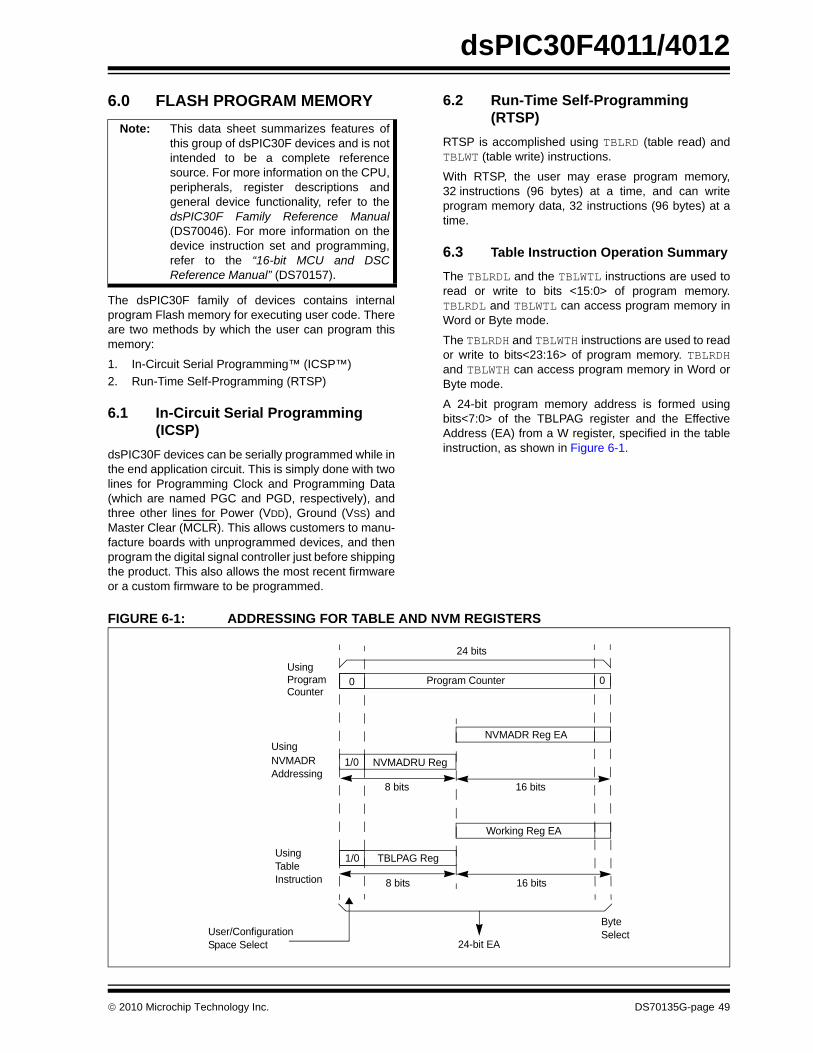
dsPIC30F4011/4012
6.0 FLASH PROGRAM MEMORY
The dsPIC30F family of devices contains internalprogram Flash memory for executing user code. Thereare two methods by which the user can program thismemory:
1. In-Circuit Serial Programming™ (ICSP™)2. Run-Time Self-Programming (RTSP)
6.1 In-Circuit Serial Programming (ICSP)
dsPIC30F devices can be serially programmed while inthe end application circuit. This is simply done with twolines for Programming Clock and Programming Data(which are named PGC and PGD, respectively), andthree other lines for Power (VDD), Ground (VSS) andMaster Clear (MCLR). This allows customers to manu-facture boards with unprogrammed devices, and thenprogram the digital signal controller just before shippingthe product. This also allows the most recent firmwareor a custom firmware to be programmed.
6.2 Run-Time Self-Programming (RTSP)
RTSP is accomplished using TBLRD (table read) andTBLWT (table write) instructions.
With RTSP, the user may erase program memory,32 instructions (96 bytes) at a time, and can writeprogram memory data, 32 instructions (96 bytes) at atime.
6.3 Table Instruction Operation Summary
The TBLRDL and the TBLWTL instructions are used toread or write to bits <15:0> of program memory.TBLRDL and TBLWTL can access program memory inWord or Byte mode.
The TBLRDH and TBLWTH instructions are used to reador write to bits<23:16> of program memory. TBLRDHand TBLWTH can access program memory in Word orByte mode.
A 24-bit program memory address is formed usingbits<7:0> of the TBLPAG register and the EffectiveAddress (EA) from a W register, specified in the tableinstruction, as shown in Figure 6-1.
FIGURE 6-1: ADDRESSING FOR TABLE AND NVM REGISTERS
Note: This data sheet summarizes features ofthis group of dsPIC30F devices and is notintended to be a complete referencesource. For more information on the CPU,peripherals, register descriptions andgeneral device functionality, refer to thedsPIC30F Family Reference Manual(DS70046). For more information on thedevice instruction set and programming,refer to the “16-bit MCU and DSCReference Manual” (DS70157).
0Program Counter
24 bits
NVMADRU Reg
8 bits 16 bits
Program
Using
TBLPAG Reg
8 bits
Working Reg EA
16 bits
Using
Byte
24-bit EA
1/0
0
1/0
Select
TableInstruction
NVMADRAddressing
Counter
Using
NVMADR Reg EA
User/ConfigurationSpace Select
© 2010 Microchip Technology Inc. DS70135G-page 49
dsPIC30F4011/4012
6.4 RTSP OperationThe dsPIC30F Flash program memory is organizedinto rows and panels. Each row consists of 32 instruc-tions or 96 bytes. Each panel consists of 128 rows or4K x 24 instructions. RTSP allows the user to erase onerow (32 instructions) at a time and to program32 instructions at one time.Each panel of program memory contains write latchesthat hold 32 instructions of programming data. Prior tothe actual programming operation, the write data mustbe loaded into the panel write latches. The data to beprogrammed into the panel is loaded in sequentialorder into the write latches: instruction 0, instruction 1,etc. The addresses loaded must always be from a32 address boundary.
The basic sequence for RTSP programming is to set upa Table Pointer, then do a series of TBLWT instructionsto load the write latches. Programming is performed bysetting the special bits in the NVMCON register.32 TBLWTL and 32 TBLWTH instructions are requiredto load the 32 instructions.
All of the table write operations are single-word writes(2 instruction cycles) because only the table latches arewritten.
After the latches are written, a programming operationneeds to be initiated to program the data.
The Flash program memory is readable, writable anderasable during normal operation over the entire VDDrange.
6.5 RTSP Control RegistersThe four SFRs used to read and write the programFlash memory are:
• NVMCON• NVMADR• NVMADRU• NVMKEY
6.5.1 NVMCON REGISTERThe NVMCON register controls which blocks are to beerased, which memory type is to be programmed andthe start of the programming cycle.
6.5.2 NVMADR REGISTERThe NVMADR register is used to hold the lower twobytes of the Effective Address. The NVMADR registercaptures the EA<15:0> of the last table instruction thathas been executed and selects the row to write.
6.5.3 NVMADRU REGISTERThe NVMADRU register is used to hold the upper byteof the Effective Address. The NVMADRU register cap-tures the EA<23:16> of the last table instruction thathas been executed.
6.5.4 NVMKEY REGISTERNVMKEY is a write-only register that is used for writeprotection. To start a programming or an erasesequence, the user must consecutively write 0x55 and0xAA to the NVMKEY register. Refer to Section 6.6“Programming Operations” for further details.
Note: The user can also directly write to theNVMADR and NVMADRU registers tospecify a program memory address forerasing or programming.
DS70135G-page 50 © 2010 Microchip Technology Inc.

dsPIC30F4011/4012
6.6 Programming OperationsA complete programming sequence is necessary forprogramming or erasing the internal Flash in RTSPmode. A programming operation is nominally 2 msec induration and the processor stalls (waits) until the oper-ation is finished. Setting the WR bit (NVMCON<15>)starts the operation, and the WR bit is automaticallycleared when the operation is finished.6.6.1 PROGRAMMING ALGORITHM FOR PROGRAM FLASH
The user can erase or program one row of programFlash memory at a time. The general process is:
1. Read one row of program Flash (32 instructionwords) and store into data RAM as a data“image”.
2. Update the data image with the desired newdata.
3. Erase program Flash row.a) Set up NVMCON register for multi-word,
program Flash, erase and set WREN bit.b) Write address of row to be erased into
NVMADRU/NVMDR.c) Write 0x55 to NVMKEY.d) Write 0xAA to NVMKEY.e) Set the WR bit. This will begin erase cycle.f) CPU will stall for the duration of the erase
cycle.g) The WR bit is cleared when erase cycle
ends.
4. Write 32 instruction words of data from dataRAM “image” into the program Flash writelatches.
5. Program 32 instruction words into programFlash.a) Set up NVMCON register for multi-word,
program Flash, program and set WREN bit.b) Write 0x55 to NVMKEY.c) Write 0xAA to NVMKEY.d) Set the WR bit. This will begin program
cycle.e) CPU will stall for duration of the program
cycle.f) The WR bit is cleared by the hardware
when program cycle ends.6. Repeat steps 1 through 5 as needed to program
desired amount of program Flash memory.
6.6.2 ERASING A ROW OF PROGRAM MEMORY
Example 6-1 shows a code sequence that can be usedto erase a row (32 instructions) of program memory.
EXAMPLE 6-1: ERASING A ROW OF PROGRAM MEMORY ; Setup NVMCON for erase operation, multi word write; program memory selected, and writes enabled
MOV #0x4041,W0 ;MOV W0,NVMCON ; Init NVMCON SFR
; Init pointer to row to be ERASEDMOV #tblpage(PROG_ADDR),W0 ; MOV W0,NVMADRU ; Initialize PM Page Boundary SFRMOV #tbloffset(PROG_ADDR),W0 ; Intialize in-page EA[15:0] pointerMOV W0, NVMADR ; Intialize NVMADR SFRDISI #5 ; Block all interrupts with priority < 7
; for next 5 instructionsMOV #0x55,W0 MOV W0,NVMKEY ; Write the 0x55 key MOV #0xAA,W1 ;MOV W1,NVMKEY ; Write the 0xAA keyBSET NVMCON,#WR ; Start the erase sequence NOP ; Insert two NOPs after the eraseNOP ; command is asserted
© 2010 Microchip Technology Inc. DS70135G-page 51
dsPIC30F4011/4012
6.6.3 LOADING WRITE LATCHESExample 6-2 shows a sequence of instructions thatcan be used to load the 96 bytes of write latches.32 TBLWTL and 32 TBLWTH instructions are needed toload the write latches selected by the Table Pointer.EXAMPLE 6-2: LOADING WRITE LATCHES
6.6.4 INITIATING THE PROGRAMMING SEQUENCE
For protection, the write initiate sequence for NVMKEYmust be used to allow any erase or program operationto proceed. After the programming command has beenexecuted, the user must wait for the programming timeuntil programming is complete. The two instructionsfollowing the start of the programming sequenceshould be NOPs.
EXAMPLE 6-3: INITIATING A PROGRAMMING SEQUENCE
; Set up a pointer to the first program memory location to be written; program memory selected, and writes enabled
MOV #0x0000,W0 ; MOV W0,TBLPAG ; Initialize PM Page Boundary SFRMOV #0x6000,W0 ; An example program memory address
; Perform the TBLWT instructions to write the latches; 0th_program_word
MOV #LOW_WORD_0,W2 ; MOV #HIGH_BYTE_0,W3 ; TBLWTL W2,[W0] ; Write PM low word into program latchTBLWTH W3,[W0++] ; Write PM high byte into program latch
; 1st_program_wordMOV #LOW_WORD_1,W2 ; MOV #HIGH_BYTE_1,W3 ; TBLWTL W2,[W0] ; Write PM low word into program latchTBLWTH W3,[W0++] ; Write PM high byte into program latch
; 2nd_program_wordMOV #LOW_WORD_2,W2 ; MOV #HIGH_BYTE_2,W3 ; TBLWTL W2, [W0] ; Write PM low word into program latchTBLWTH W3, [W0++] ; Write PM high byte into program latch•••
; 31st_program_wordMOV #LOW_WORD_31,W2 ; MOV #HIGH_BYTE_31,W3 ; TBLWTL W2, [W0] ; Write PM low word into program latchTBLWTH W3, [W0++] ; Write PM high byte into program latch
Note: In Example 6-2, the contents of the upper byte of W3 have no effect.
DISI #5 ; Block all interrupts with priority < 7; for next 5 instructions
MOV #0x55,W0MOV W0,NVMKEY ; Write the 0x55 key MOV #0xAA,W1 ;MOV W1,NVMKEY ; Write the 0xAA keyBSET NVMCON,#WR ; Start the erase sequence NOP ; Insert two NOPs after the eraseNOP ; command is asserted
DS70135G-page 52 © 2010 Microchip Technology Inc.

© 2010 M
icrochip Technology Inc.D
S70135G
-page 53
dsPIC30F4011/4012
TAF 1 Bit 0 All Resets
NV 0000 0000 0000 0000
NV uuuu uuuu uuuu uuuu
NV 0000 0000 uuuu uuuu
NV 0000 0000 0000 0000
LeNo
BLE 6-1: NVM REGISTER MAP(1)
ile Name Addr. Bit 15 Bit 14 Bit 13 Bit 12 Bit 11 Bit 10 Bit 9 Bit 8 Bit 7 Bit 6 Bit 5 Bit 4 Bit 3 Bit 2 Bit
MCON 0760 WR WREN WRERR — — — — TWRI — PROGOP<6:0>
MADR 0762 NVMADR<15:0>
MADRU 0764 — — — — — — — — — NVMADR<22:16>
MKEY 0766 — — — — — — — — KEY<7:0>
gend: u = uninitialized bit; — = unimplemented bit, read as ‘0’te 1: Refer to the “dsPIC30F Family Reference Manual” (DS70046) for descriptions of register bit fields.

dsPIC30F4011/4012
NOTES:DS70135G-page 54 © 2010 Microchip Technology Inc.

dsPIC30F4011/4012
7.0 DATA EEPROM MEMORY
The data EEPROM memory is readable and writableduring normal operation over the entire VDD range. Thedata EEPROM memory is directly mapped in theprogram memory address space.
The four SFRs used to read and write the programFlash memory are used to access data EEPROMmemory, as well. As described in Section 6.0 “FlashProgram Memory”, these registers are:
• NVMCON• NVMADR• NVMADRU• NVMKEY
The EEPROM data memory allows read and write ofsingle words and 16-word blocks. When interfacing todata memory, NVMADR, in conjunction with theNVMADRU register, is used to address the EEPROMlocation being accessed. TBLRDL and TBLWTL instruc-tions are used to read and write data EEPROM. ThedsPIC30F4011/4012 devices have 1 Kbyte (512 words)of data EEPROM, with an address range from0x7FFC00 to 0x7FFFFE.
A word write operation should be preceded by an eraseof the corresponding memory location(s). The writetypically requires 2 ms to complete, but the write timewill vary with voltage and temperature.
A program or erase operation on the data EEPROMdoes not stop the instruction flow. The user is respon-sible for waiting for the appropriate duration of timebefore initiating another data EEPROM write/eraseoperation. Attempting to read the data EEPROM whilea programming or erase operation is in progress resultsin unspecified data.
Control bit, WR, initiates write operations, similar toprogram Flash writes. This bit cannot be cleared, onlyset, in software. This bit is cleared in hardware at thecompletion of the write operation. The inability to clearthe WR bit in software prevents the accidental orpremature termination of a write operation.
The WREN bit, when set, will allow a write operation.On power-up, the WREN bit is clear. The WRERR bit isset when a write operation is interrupted by a MCLRReset, or a WDT Time-out Reset, during normal oper-ation. In these situations, following Reset, the user cancheck the WRERR bit and rewrite the location. Theaddress register, NVMADR, remains unchanged.
7.1 Reading the Data EEPROM A TBLRD instruction reads a word at the current pro-gram word address. This example uses W0 as apointer to data EEPROM. The result is placed inregister W4, as shown in Example 7-1.
EXAMPLE 7-1: DATA EEPROM READ
Note: This data sheet summarizes features ofthis group of dsPIC30F devices and is notintended to be a complete referencesource. For more information on the CPU,peripherals, register descriptions andgeneral device functionality, refer to thedsPIC30F Family Reference Manual(DS70046). For more information on thedevice instruction set and programming,refer to the “16-bit MCU and DSCReference Manual” (DS70157).
Note: Interrupt flag bit, NVMIF in the IFS0register, is set when write is complete. Itmust be cleared in software.
MOV #LOW_ADDR_WORD,W0 ; Init PointerMOV #HIGH_ADDR_WORD,W1MOV W1,TBLPAG TBLRDL [ W0 ], W4 ; read data EEPROM
© 2010 Microchip Technology Inc. DS70135G-page 55

dsPIC30F4011/4012
7.2 Erasing Data EEPROM7.2.1 ERASING A BLOCK OF DATA EEPROM
In order to erase a block of data EEPROM, theNVMADRU and NVMADR registers must initiallypoint to the block of memory to be erased. ConfigureNVMCON for erasing a block of data EEPROM andset the WR and WREN bits in the NVMCON register.Setting the WR bit initiates the erase, as shown inExample 7-2.
EXAMPLE 7-2: DATA EEPROM BLOCK ERASE
7.2.2 ERASING A WORD OF DATA EEPROM
The TBLPAG and NVMADR registers must point tothe block. Select erase a block of data Flash and setthe WR and WREN bits in the NVMCON register.Setting the WR bit initiates the erase, as shown inExample 7-3.
EXAMPLE 7-3: DATA EEPROM WORD ERASE
; Select data EEPROM block, WR, WREN bitsMOV #0x4045,W0MOV W0,NVMCON ; Initialize NVMCON SFR
; Start erase cycle by setting WR after writing key sequence
DISI #5 ; Block all interrupts with priority < 7; for next 5 instructions
MOV #0x55,W0 ; MOV W0,NVMKEY ; Write the 0x55 key
MOV #0xAA,W1 ;MOV W1,NVMKEY ; Write the 0xAA keyBSET NVMCON,#WR ; Initiate erase sequence
NOP NOP; Erase cycle will complete in 2mS. CPU is not stalled for the Data Erase Cycle; User can poll WR bit, use NVMIF or Timer IRQ to determine erasure complete
; Select data EEPROM word, WR, WREN bitsMOV #0x4044,W0MOV W0,NVMCON
; Start erase cycle by setting WR after writing key sequence
DISI #5 ; Block all interrupts with priority <7; for next 5 instructions
MOV #0x55,W0 ; MOV W0,NVMKEY ; Write the 0x55 keyMOV #0xAA,W1 ;MOV W1,NVMKEY ; Write the 0xAA keyBSET NVMCON,#WR ; Initiate erase sequence
NOP NOP ; Erase cycle will complete in 2mS. CPU is not stalled for the Data Erase Cycle; User can poll WR bit, use NVMIF or Timer IRQ to determine erasure complete
DS70135G-page 56 © 2010 Microchip Technology Inc.

dsPIC30F4011/4012
7.3 Writing to the Data EEPROM To write an EEPROM data location, the followingsequence must be followed:1. Erase data EEPROM word.a) Select word, data EEPROM; erase and set
WREN bit in NVMCON register.b) Write address of word to be erased into
NVMADRU/NVMADR.c) Enable NVM interrupt (optional).d) Write 0x55 to NVMKEY.e) Write 0xAA to NVMKEY.f) Set the WR bit. This will begin erase cycle.g) Either poll NVMIF bit or wait for NVMIF
interrupt.h) The WR bit is cleared when the erase cycle
ends.2. Write data word into data EEPROM write
latches.3. Program 1 data word into data EEPROM.
a) Select word, data EEPROM; program andset WREN bit in NVMCON register.
b) Enable NVM write done interrupt (optional).c) Write 0x55 to NVMKEY.d) Write 0xAA to NVMKEY.e) Set the WR bit. This will begin program
cycle.f) Either poll NVMIF bit or wait for NVM
interrupt.g) The WR bit is cleared when the write cycle
ends.
The write will not initiate if the above sequence is notexactly followed (write 0x55 to NVMKEY, write 0xAA toNVMCON, then set WR bit) for each word. It is stronglyrecommended that interrupts be disabled during thiscode segment.
Additionally, the WREN bit in NVMCON must be set toenable writes. This mechanism prevents accidentalwrites to data EEPROM due to unexpected code exe-cution. The WREN bit should be kept clear at all timesexcept when updating the EEPROM. The WREN bit isnot cleared by hardware.
After a write sequence has been initiated, clearing theWREN bit will not affect the current write cycle. The WRbit will be inhibited from being set unless the WREN bitis set. The WREN bit must be set on a previousinstruction. Both WR and WREN cannot be set with thesame instruction.
At the completion of the write cycle, the WR bit iscleared in hardware and the Nonvolatile Memory WriteComplete Interrupt Flag bit (NVMIF) is set. The usermay either enable this interrupt or poll this bit. NVMIFmust be cleared by software.
7.3.1 WRITING A WORD OF DATA EEPROM
Once the user has erased the word to be programmed,then a table write instruction is used to write one writelatch, as shown in Example 7-4.
EXAMPLE 7-4: DATA EEPROM WORD WRITE; Point to data memory
MOV #LOW_ADDR_WORD,W0 ; Init pointerMOV #HIGH_ADDR_WORD,W1MOV W1,TBLPAGMOV #LOW(WORD),W2 ; Get dataTBLWTL W2,[ W0] ; Write data
; The NVMADR captures last table access address; Select data EEPROM for 1 word op
MOV #0x4004,W0MOV W0,NVMCON
; Operate key to allow write operation
DISI #5 ; Block all interrupts with priority < 7; for next 5 instructions
MOV #0x55,W0MOV W0,NVMKEY ; Write the 0x55 keyMOV #0xAA,W1MOV W1,NVMKEY ; Write the 0xAA keyBSET NVMCON,#WR ; Initiate program sequence
NOP NOP ; Write cycle will complete in 2mS. CPU is not stalled for the Data Write Cycle; User can poll WR bit, use NVMIF or Timer IRQ to determine write complete
© 2010 Microchip Technology Inc. DS70135G-page 57

dsPIC30F4011/4012
7.3.2 WRITING A BLOCK OF DATAEEPROMTo write a block of data EEPROM, write to all sixteenlatches first, then set the NVMCON register andprogram the block.
EXAMPLE 7-5: DATA EEPROM BLOCK WRITE MOV #LOW_ADDR_WORD,W0 ; Init pointer MOV #HIGH_ADDR_WORD,W1 MOV W1,TBLPAG MOV #data1,W2 ; Get 1st data TBLWTL W2,[ W0]++ ; write data MOV #data2,W2 ; Get 2nd data TBLWTL W2,[ W0]++ ; write data MOV #data3,W2 ; Get 3rd data TBLWTL W2,[ W0]++ ; write data MOV #data4,W2 ; Get 4th data TBLWTL W2,[ W0]++ ; write data MOV #data5,W2 ; Get 5th data TBLWTL W2,[ W0]++ ; write data MOV #data6,W2 ; Get 6th data TBLWTL W2,[ W0]++ ; write data MOV #data7,W2 ; Get 7th data TBLWTL W2,[ W0]++ ; write data MOV #data8,W2 ; Get 8th data TBLWTL W2,[ W0]++ ; write data MOV #data9,W2 ; Get 9th data TBLWTL W2,[ W0]++ ; write data MOV #data10,W2 ; Get 10th data TBLWTL W2,[ W0]++ ; write data MOV #data11,W2 ; Get 11th data TBLWTL W2,[ W0]++ ; write data MOV #data12,W2 ; Get 12th data TBLWTL W2,[ W0]++ ; write data MOV #data13,W2 ; Get 13th data TBLWTL W2,[ W0]++ ; write data MOV #data14,W2 ; Get 14th data TBLWTL W2,[ W0]++ ; write data MOV #data15,W2 ; Get 15th data TBLWTL W2,[ W0]++ ; write data MOV #data16,W2 ; Get 16th data TBLWTL W2,[ W0]++ ; write data. The NVMADR captures last table access address. MOV #0x400A,W0 ; Select data EEPROM for multi word op
MOV W0,NVMCON ; Operate Key to allow program operationDISI #5 ; Block all interrupts with priority < 7
; for next 5 instructions MOV #0x55,W0 MOV W0,NVMKEY ; Write the 0x55 key MOV #0xAA,W1 MOV W1,NVMKEY ; Write the 0xAA key BSET NVMCON,#WR ; Start write cycle NOP NOP
DS70135G-page 58 © 2010 Microchip Technology Inc.

dsPIC30F4011/4012
7.4 Write VerifyDepending on the application, good programmingpractice may dictate that the value written to the mem-ory should be verified against the original value. Thisshould be used in applications where excessive writescan stress bits near the specification limit.7.5 Protection Against Spurious WriteThere are conditions when the device may not want towrite to the data EEPROM memory. To protect againstspurious EEPROM writes, various mechanisms havebeen built-in. On power-up, the WREN bit is cleared;also, the Power-up Timer prevents EEPROM write.
Together, the write initiate sequence and the WREN bithelp prevent an accidental write during brown-out,power glitch or software malfunction.
© 2010 Microchip Technology Inc. DS70135G-page 59

dsPIC30F4011/4012
NOTES:DS70135G-page 60 © 2010 Microchip Technology Inc.
dsPIC30F4011/4012
8.0 I/O PORTS
All of the device pins (except VDD, VSS, MCLR andOSC1/CLKI) are shared between the peripherals andthe parallel I/O ports.
All I/O input ports feature Schmitt Trigger inputs forimproved noise immunity.
8.1 Parallel I/O (PIO) PortsWhen a peripheral is enabled and the peripheral isactively driving an associated pin, the use of the pin asa general purpose output pin is disabled. The I/O pinmay be read, but the output driver for the Parallel Portbit will be disabled. If a peripheral is enabled, but theperipheral is not actively driving a pin, that pin may bedriven by a port.
All port pins have three registers directly associatedwith the operation of the port pin. The Data Directionregister (TRISx) determines whether the pin is an inputor an output. If the Data Direction register bit is a ‘1’,then the pin is an input. All port pins are defined asinputs after a Reset. Reads from the latch (LATx), read
the latch. Writes to the latch, write the latch (LATx).Reads from the port (PORTx), read the port pins andwrites to the port pins, write the latch (LATx).
Any bit and its associated data and control registersthat are not valid for a particular device will bedisabled. That means the corresponding LATx andTRISx registers and the port pin will read as zeros.
When a pin is shared with another peripheral or func-tion that is defined as an input only, it is neverthelessregarded as a dedicated port because there is noother competing source of outputs. An example is theINT4 pin.
The format of the registers for PORTx are shown inTable 8-1.
The TRISx (Data Direction) register controls the direc-tion of the pins. The LATx register supplies data to theoutputs and is readable/writable. Reading the PORTxregister yields the state of the input pins, while writingto the PORTx register modifies the contents of theLATx register.
A parallel I/O (PIO) port that shares a pin with a periph-eral is, in general, subservient to the peripheral. Theperipheral’s output buffer data and control signals areprovided to a pair of multiplexers. The multiplexersselect whether the peripheral or the associated porthas ownership of the output data and control signals ofthe I/O pad cell. Figure 8-2 shows how ports are sharedwith other peripherals and the associated I/O cell (pad)to which they are connected. Table 8-1 and Table 8-2show the formats of the registers for the shared ports,PORTB through PORTG.
FIGURE 8-1: BLOCK DIAGRAM OF A DEDICATED PORT STRUCTURE
Note: This data sheet summarizes features ofthis group of dsPIC30F devices and is notintended to be a complete referencesource. For more information on the CPU,peripherals, register descriptions andgeneral device functionality, refer to thedsPIC30F Family Reference Manual(DS70046). For more information on thedevice instruction set and programming,refer to the “16-bit MCU and DSCReference Manual” (DS70157).
QD
CK
WR LAT +
TRIS Latch
I/O Pad
WR PORT
Data Bus
QD
CK
Data Latch
Read LAT
Read PORT
Read TRIS
WR TRIS
I/O Cell
Dedicated Port Module
© 2010 Microchip Technology Inc. DS70135G-page 61

dsPIC30F4011/4012
FIGURE 8-2: BLOCK DIAGRAM OF A SHARED PORT STRUCTURE8.2 Configuring Analog Port PinsThe use of the ADPCFG and TRIS registers control theoperation of the A/D port pins. The port pins that aredesired as analog inputs must have their correspond-ing TRIS bit set (input). If the TRIS bit is cleared(output), the digital output level (VOH or VOL) will beconverted.
When reading the PORT register, all pins configured asanalog input channels will read as cleared (a low level).
Pins configured as digital inputs will not convert an ana-log input. Analog levels on any pin that is defined as adigital input (including the ANx pins), may cause theinput buffer to consume current that exceeds thedevice specifications.
8.2.1 I/O PORT WRITE/READ TIMINGOne instruction cycle is required between a portdirection change or port write operation and a readoperation of the same port. Typically this instructionwould be a NOP.
EXAMPLE 8-1: PORT WRITE/READ EXAMPLE
QD
CK
WR LAT +
TRIS Latch
I/O Pad
WR PORT
Data Bus
QD
CK
Data Latch
Read LAT
Read PORT
Read TRIS
1
0
1
0
WR TRIS
Peripheral Output Data
Peripheral Input Data
I/O Cell
Peripheral Module
Peripheral Output Enable
PIO Module
Output Multiplexers
Input Data
Peripheral Module Enable
Output Enable
Output Data
MOV 0xFF00, W0 ; Configure PORTB<15:8>; as inputs
MOV W0, TRISBB ; and PORTB<7:0> as outputsNOP ; Delay 1 cycleBTSS PORTB, #13 ; Next Instruction
DS70135G-page 62 © 2010 Microchip Technology Inc.

© 2010 M
icrochip Technology Inc.D
S70135G
-page 63
dsPIC30F4011/4012
TA
Bit 1 Bit 0 Reset State
TR TRISB1 TRISB0 0000 0001 1111 1111
PO RB1 RB0 0000 0000 0000 0000
LA LATB1 LATB0 0000 0000 0000 0000
TR — — 1110 0000 0000 0000
PO — — 0000 0000 0000 0000
LA — — 0000 0000 0000 0000
TR TRISD1 TRISD0 0000 0000 0000 1111
PO RD1 RD0 0000 0000 0000 0000
LA LATD1 LATD0 0000 0000 0000 0000
TR TRISE1 TRISE0 0000 0001 0011 1111
PO RE1 RE0 0000 0000 0000 0000
LA LATE1 LATE0 0000 0000 0000 0000
TR TRISF1 TRISF0 0000 0000 0111 1111
PO RF1 RF0 0000 0000 0000 0000
LA LATF1 LATF0 0000 0000 0000 0000
LeNo
BLE 8-1: dsPIC30F4011 PORT REGISTER MAP(1)
SFR Name Addr. Bit 15 Bit 14 Bit 13 Bit 12 Bit 11 Bit 10 Bit 9 Bit 8 Bit 7 Bit 6 Bit 5 Bit 4 Bit 3 Bit 2
ISB 02C6 — — — — — — — TRISB8 TRISB7 TRISB6 TRISB5 TRISB4 TRISB3 TRISB2
RTB 02C8 — — — — — — — RB8 RB7 RB6 RB5 RB4 RB3 RB2
TB 02CA — — — — — — — LATB8 LATB7 LATB6 LATB5 LATB4 LATB3 LATB2
ISC 02CC TRISC15 TRISC14 TRISC13 — — — — — — — — — — —
RTC 02CE RC15 RC14 RC13 — — — — — — — — — — —
TC 02D0 LATC15 LATC14 LATC13 — — — — — — — — — — —
ISD 02D2 — — — — — — — — — — — — TRISD3 TRISD2
RTD 02D4 — — — — — — — — — — — — RD3 RD2
TD 02D6 — — — — — — — — — — — — LATD3 LATD2
ISE 02D8 — — — — — — — TRISE8 — — TRISE5 TRISE4 TRISE3 TRISE2
RTE 02DA — — — — — — — RE8 — — RE5 RE4 RE3 RE2
TE 02DC — — — — — — — LATE8 — — LATE5 LATE4 LATE3 LATE2
ISF 02DE — — — — — — — — — TRISF6 TRISF5 TRISF4 TRISF3 TRISF2
RTF 02E0 — — — — — — — — — RF6 RF5 RF4 RF3 RF2
TF 02E2 — — — — — — — — — LATF6 LATF5 LATF4 LATF3 LATF2
gend: — = unimplemented bit, read as ‘0’te 1: Refer to the “dsPIC30F Family Reference Manual” (DS70046) for descriptions of register bit fields.

dsPIC30F4011/4012
DS
70135G-page 64
© 2010 M
icrochip Technology Inc.
Bit 2 Bit 1 Bit 0 Reset State
RISB2 TRISB1 TRISB0 0000 0000 0011 1111
RB2 RB1 RB0 0000 0000 0000 0000
ATB2 LATB1 LATB0 0000 0000 0000 0000
— — — 1110 0000 0000 0000
— — — 0000 0000 0000 0000
— — — 0000 0000 0000 0000
— TRISD1 TRISD0 0000 0000 0000 0011
— RD1 RD0 0000 0000 0000 0000
— LATD1 LATD0 0000 0000 0000 0000
RISE2 TRISE1 TRISE0 0000 0001 0011 1111
RE2 RE1 RE0 0000 0000 0000 0000
ATE2 LATE1 LATE0 0000 0000 0000 0000
RISF2 — — 0000 0000 0000 1100
RF2 — — 0000 0000 0000 0000
ATF2 — — 0000 0000 0000 0000
TABLE 8-2: dsPIC30F4012 PORT REGISTER MAP(1)
SFR Name Addr. Bit 15 Bit 14 Bit 13 Bit 12 Bit 11 Bit 10 Bit 9 Bit 8 Bit 7 Bit 6 Bit 5 Bit 4 Bit 3
TRISB 02C6 — — — — — — — — — — TRISB5 TRISB4 TRISB3 T
PORTB 02C8 — — — — — — — — — — RB5 RB4 RB3
LATB 02CB — — — — — — — — — — LATB5 LATB4 LATB3 L
TRISC 02CC TRISC15 TRISC14 TRISC13 — — — — — — — — — —
PORTC 02CE RC15 RC14 RC13 — — — — — — — — — —
LATC 02D0 LATC15 LATC14 LATC13 — — — — — — — — — —
TRISD 02D2 — — — — — — — — — — — — —
PORTD 02D4 — — — — — — — — — — — — —
LATD 02D6 — — — — — — — — — — — — —
TRISE 02D8 — — — — — — — TRISE8 — — TRISE5 TRISE4 TRISE3 T
PORTE 02DA — — — — — — — RE8 — — RE5 RE4 RE3
LATE 02DC — — — — — — — LATE8 — — LATE5 LATE4 LATE3 L
TRISF 02EE — — — — — — — — — — — — TRISF3 T
PORTF 02E0 — — — — — — — — — — — — RF3
LATF 02E2 — — — — — — — — — — — — LATF3 L
Legend: — = unimplemented bit, read as ‘0’Note 1: Refer to the “dsPIC30F Family Reference Manual” (DS70046) for descriptions of register bit fields.

dsPIC30F4011/4012
8.3 Input Change Notification ModuleThe input change notification module provides thedsPIC30F devices the ability to generate interruptrequests to the processor in response to a change ofstate on selected input pins. This module is capable ofdetecting input change of states, even in Sleep mode,when the clocks are disabled. There are 10 externalsignals (CN0 through CN7, CN17 and CN18) that maybe selected (enabled) for generating an interruptrequest on a change of state.Please refer to the pin diagrams for CN pin locations.
TABLE 8-3: INPUT CHANGE NOTIFICATION REGISTER MAP (BITS 7-0)(1)
SFR Name Addr. Bit 7 Bit 6 Bit 5 Bit 4 Bit 3 Bit 2 Bit 1 Bit 0 Reset State
CNEN1 00C0 CN7IE CN6IE CN5IE CN4IE CN3IE CN2IE CN1IE CN0IE 0000 0000 0000 0000
CNEN2 00C2 — — — — — CN18IE(2) CN17IE(2) — 0000 0000 0000 0000
CNPU1 00C4 CN7PUE CN6PUE CN5PUE CN4PUE CN3PUE CN2PUE CN1PUE CN0PUE 0000 0000 0000 0000
CNPU2 00C6 — — — — — CN18PUE(2) CN17PUE(2) — 0000 0000 0000 0000
Legend: u = uninitialized bit; — = unimplemented bit, read as ‘0’Note 1: Refer to the “dsPIC30F Family Reference Manual” (DS70046) for descriptions of register bit fields.
2: These bits are not available on dsPIC30F4012 devices.
© 2010 Microchip Technology Inc. DS70135G-page 65

dsPIC30F4011/4012
NOTES:DS70135G-page 66 © 2010 Microchip Technology Inc.

dsPIC30F4011/4012
9.0 TIMER1 MODULE
This section describes the 16-bit general purposeTimer1 module and associated operational modes.Figure 9-1 depicts the simplified block diagram of the16-bit Timer1 module.
The following sections provide a detailed description,including setup and control registers, along with asso-ciated block diagrams for the operational modes of thetimers.
The Timer1 module is a 16-bit timer which can serve asthe time counter for the Real-Time Clock, or operate asa free-running, interval timer/counter. The 16-bit timerhas the following modes:
• 16-bit Timer• 16-bit Synchronous Counter• 16-bit Asynchronous Counter
Further, the following operational characteristics aresupported:
• Timer gate operation• Selectable prescaler settings• Timer operation during CPU Idle and Sleep
modes• Interrupt on 16-bit Period register match or falling
edge of external gate signal
These operating modes are determined by setting theappropriate bit(s) in the 16-bit SFR, T1CON. Figure 9-1presents a block diagram of the 16-bit timer module.
16-bit Timer Mode: In the 16-bit Timer mode, the timerincrements on every instruction cycle up to a matchvalue, preloaded into the Period register, PR1, thenresets to 0 and continues to count.
When the CPU goes into the Idle mode, the timer willstop incrementing unless the TSIDL (T1CON<13>)bit = 0. If TSIDL = 1, the timer module logic will resumethe incrementing sequence upon termination of theCPU Idle mode.
16-bit Synchronous Counter Mode: In the 16-bitSynchronous Counter mode, the timer increments onthe rising edge of the applied external clock signal,which is synchronized with the internal phase clocks.The timer counts up to a match value preloaded in PR1,then resets to 0 and continues.
When the CPU goes into the Idle mode, the timer willstop incrementing unless the respective TSIDL bit = 0.If TSIDL = 1, the timer module logic will resume theincrementing sequence upon termination of the CPUIdle mode.
16-bit Asynchronous Counter Mode: In the 16-bitAsynchronous Counter mode, the timer increments onevery rising edge of the applied external clock signal.The timer counts up to a match value preloaded in PR1,then resets to 0 and continues.
When the timer is configured for the Asynchronous modeof operation, and the CPU goes into the Idle mode, thetimer will stop incrementing if TSIDL = 1.
Note: This data sheet summarizes features ofthis group of dsPIC30F devices and is notintended to be a complete referencesource. For more information on the CPU,peripherals, register descriptions andgeneral device functionality, refer to thedsPIC30F Family Reference Manual(DS70046). For more information on thedevice instruction set and programming,refer to the “16-bit MCU and DSCReference Manual” (DS70157).
Note: Timer1 is a ‘Type A’ timer. Please refer tothe specifications for a Type A timer inSection 24.0 “Electrical Characteristics”of this document.
© 2010 Microchip Technology Inc. DS70135G-page 67

dsPIC30F4011/4012
FIGURE 9-1: 16-BIT TIMER1 MODULE BLOCK DIAGRAM (TYPE A TIMER)9.1 Timer Gate OperationThe 16-bit timer can be placed in the Gated Time Accu-mulation mode. This mode allows the internal TCY toincrement the respective timer when the gate inputsignal (T1CK pin) is asserted high. Control bit, TGATE(T1CON<6>), must be set to enable this mode. Thetimer must be enabled (TON = 1) and the timer clocksource set to internal (TCS = 0).
When the CPU goes into the Idle mode, the timer willstop incrementing unless TSIDL = 0. If TSIDL = 1, thetimer will resume the incrementing sequence upontermination of the CPU Idle mode.
9.2 Timer PrescalerThe input clock (FOSC/4 or external clock) to the 16-bitTimer has a prescale option of 1:1, 1:8, 1:64 and 1:256selected by control bits, TCKPS<1:0> (T1CON<5:4>).The prescaler counter is cleared when any of thefollowing occurs:
• A write to the TMR1 register• Clearing of the TON bit (T1CON<15>)• A device Reset, such as a POR and BOR
However, if the timer is disabled (TON = 0), then thetimer prescaler cannot be reset since the prescalerclock is halted.
The TMR1 register is not cleared when the T1CONregister is written. It is cleared by writing to the TMR1register.
9.3 Timer Operation During Sleep Mode
During CPU Sleep mode, the timer will operate if:
• The timer module is enabled (TON = 1) and • The timer clock source is selected as external
(TCS = 1) and• The TSYNC bit (T1CON<2>) is asserted to a logic
‘0’, which defines the external clock source as asynchronous
When all three conditions are true, the timer willcontinue to count up to the Period register and be resetto 0x0000.
When a match between the timer and the Period regis-ter occurs, an interrupt can be generated if therespective timer interrupt enable bit is asserted.
TON
Sync
SOSCI
SOSCO/
PR1
T1IF
EqualComparator x 16
TMR1Reset
LPOSCEN
Event Flag
1
0
TSYNC
Q
Q D
CK
TGATE
TCKPS<1:0>
Prescaler 1, 8, 64, 256
2
TGATE
TCY
1
0
T1CK
TCS
1 x
0 1
TGAT
E
0 0
GateSync
DS70135G-page 68 © 2010 Microchip Technology Inc.
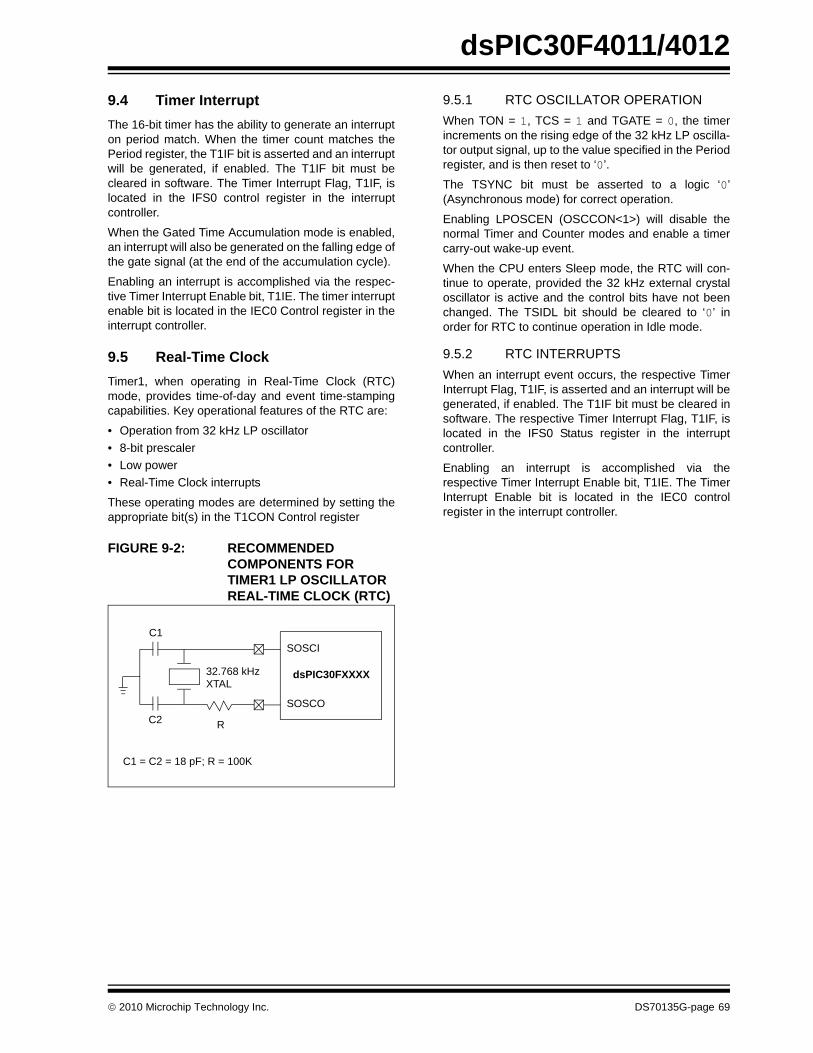
dsPIC30F4011/4012
9.4 Timer InterruptThe 16-bit timer has the ability to generate an interrupton period match. When the timer count matches thePeriod register, the T1IF bit is asserted and an interruptwill be generated, if enabled. The T1IF bit must becleared in software. The Timer Interrupt Flag, T1IF, islocated in the IFS0 control register in the interruptcontroller.When the Gated Time Accumulation mode is enabled,an interrupt will also be generated on the falling edge ofthe gate signal (at the end of the accumulation cycle).
Enabling an interrupt is accomplished via the respec-tive Timer Interrupt Enable bit, T1IE. The timer interruptenable bit is located in the IEC0 Control register in theinterrupt controller.
9.5 Real-Time ClockTimer1, when operating in Real-Time Clock (RTC)mode, provides time-of-day and event time-stampingcapabilities. Key operational features of the RTC are:
• Operation from 32 kHz LP oscillator• 8-bit prescaler• Low power • Real-Time Clock interrupts
These operating modes are determined by setting theappropriate bit(s) in the T1CON Control register
FIGURE 9-2: RECOMMENDED COMPONENTS FOR TIMER1 LP OSCILLATOR REAL-TIME CLOCK (RTC)
9.5.1 RTC OSCILLATOR OPERATIONWhen TON = 1, TCS = 1 and TGATE = 0, the timerincrements on the rising edge of the 32 kHz LP oscilla-tor output signal, up to the value specified in the Periodregister, and is then reset to ‘0’.
The TSYNC bit must be asserted to a logic ‘0’(Asynchronous mode) for correct operation.
Enabling LPOSCEN (OSCCON<1>) will disable thenormal Timer and Counter modes and enable a timercarry-out wake-up event.
When the CPU enters Sleep mode, the RTC will con-tinue to operate, provided the 32 kHz external crystaloscillator is active and the control bits have not beenchanged. The TSIDL bit should be cleared to ‘0’ inorder for RTC to continue operation in Idle mode.
9.5.2 RTC INTERRUPTSWhen an interrupt event occurs, the respective TimerInterrupt Flag, T1IF, is asserted and an interrupt will begenerated, if enabled. The T1IF bit must be cleared insoftware. The respective Timer Interrupt Flag, T1IF, islocated in the IFS0 Status register in the interruptcontroller.
Enabling an interrupt is accomplished via therespective Timer Interrupt Enable bit, T1IE. The TimerInterrupt Enable bit is located in the IEC0 controlregister in the interrupt controller.
SOSCI
SOSCO
R
C1
C2
dsPIC30FXXXX32.768 kHzXTAL
C1 = C2 = 18 pF; R = 100K
© 2010 Microchip Technology Inc. DS70135G-page 69

dsPIC30F4011/4012
DS
70135G-page 70
© 2010 M
icrochip Technology Inc.
Bit 2 Bit 1 Bit 0 Reset State
uuuu uuuu uuuu uuuu
1111 1111 1111 1111
SYNC TCS — 0000 0000 0000 0000
TABLE 9-1: TIMER1 REGISTER MAP(1)
SFR Name Addr. Bit 15 Bit 14 Bit 13 Bit 12 Bit 11 Bit 10 Bit 9 Bit 8 Bit 7 Bit 6 Bit 5 Bit 4 Bit 3
TMR1 0100 Timer1 Register
PR1 0102 Period Register 1
T1CON 0104 TON — TSIDL — — — — — — TGATE TCKPS1 TCKPS0 — T
Legend: u = uninitialized bit; — = unimplemented bit, read as ‘0’Note 1: Refer to the “dsPIC30F Family Reference Manual” (DS70046) for descriptions of register bit fields.

dsPIC30F4011/4012
10.0 TIMER2/3 MODULE
This section describes the 32-bit general purpose timermodule (Timer2/3) and associated operational modes.Figure 10-1 depicts the simplified block diagram of the32-bit Timer2/3 module. Figure 10-2 and Figure 10-3show Timer2/3 configured as two independent 16-bittimers, Timer2 and Timer3, respectively.
The Timer2/3 module is a 32-bit timer, which can beconfigured as two 16-bit timers, with selectable operat-ing modes. These timers are utilized by otherperipheral modules, such as:
• Input Capture• Output Compare/Simple PWM
The following sections provide a detailed description,including setup and control registers, along with asso-ciated block diagrams for the operational modes of thetimers.
The 32-bit timer has the following modes:
• Two independent 16-bit timers (Timer2 and Timer3) with all 16-bit operating modes (except Asynchronous Counter mode)
• Single 32-bit timer operation• Single 32-bit synchronous counter
Further, the following operational characteristics aresupported:
• ADC Event Trigger• Timer Gate Operation• Selectable Prescaler Settings• Timer Operation During Idle and Sleep Modes• Interrupt on a 32-bit Period Register Match
These operating modes are determined by setting theappropriate bit(s) in the 16-bit T2CON and T3CONSFRs.
For 32-bit timer/counter operation, Timer2 is the leastsignificant word and Timer3 is the most significant wordof the 32-bit timer.
16-bit Mode: In the 16-bit mode, Timer2 and Timer3can be configured as two independent 16-bit timers.Each timer can be set up in either 16-bit Timer mode or16-bit Synchronous Counter mode. See Section 9.0“Timer1 Module”, Timer1 Module, for details on thesetwo operating modes.
The only functional difference between Timer2 andTimer3 is that Timer2 provides synchronization of theclock prescaler output. This is useful for high-frequencyexternal clock inputs.
32-bit Timer Mode: In the 32-bit Timer mode, the timerincrements on every instruction cycle up to a matchvalue, preloaded into the combined 32-bit Periodregister, PR3/PR2, then resets to 0 and continues tocount.
For synchronous 32-bit reads of the Timer2/Timer3pair, reading the least significant word (TMR2 register)will cause the msw to be read and latched into a 16-bitholding register, termed TMR3HLD.
For synchronous 32-bit writes, the holding register(TMR3HLD) must first be written to. When followed bya write to the TMR2 register, the contents of TMR3HLDwill be transferred and latched into the MSB of the32-bit timer (TMR3).
32-bit Synchronous Counter Mode: In the 32-bitSynchronous Counter mode, the timer increments onthe rising edge of the applied external clock signal,which is synchronized with the internal phase clocks.The timer counts up to a match value preloaded in thecombined 32-bit period register, PR3/PR2, then resetsto 0 and continues.
When the timer is configured for the SynchronousCounter mode of operation and the CPU goes into theIdle mode, the timer will stop incrementing unless theTSIDL (T2CON<13>) bit = 0. If TSIDL = 1, the timermodule logic will resume the incrementing sequenceupon termination of the CPU Idle mode.
Note: This data sheet summarizes features ofthis group of dsPIC30F devices and is notintended to be a complete referencesource. For more information on the CPU,peripherals, register descriptions andgeneral device functionality, refer to thedsPIC30F Family Reference Manual(DS70046). For more information on thedevice instruction set and programming,refer to the “16-bit MCU and DSCReference Manual” (DS70157).
Note: Timer2 is a ‘Type B’ timer and Timer3 is a‘Type C’ timer. Please refer to theappropriate timer type in Section 24.0“Electrical Characteristics” of thisdocument.
Note: For 32-bit timer operation, T3CON controlbits are ignored. Only T2CON control bitsare used for setup and control. Timer2clock and gate inputs are utilized for the32-bit timer module, but an interrupt isgenerated with the Timer3 Interrupt Flag(T3IF) and the interrupt is enabled with theTimer3 Interrupt Enable bit (T3IE).
© 2010 Microchip Technology Inc. DS70135G-page 71

dsPIC30F4011/4012
FIGURE 10-1: 32-BIT TIMER2/3 BLOCK DIAGRAMTMR3 TMR2
T3IF
Equal Comparator x 32
PR3 PR2
Reset
LSB MSB
Event Flag
Note: Timer configuration bit, T32 (T2CON<3>), must be set to ‘1’ for a 32-bit timer/counter operation. All controlbits are respective to the T2CON register.
Data Bus<15:0>
TMR3HLD
Read TMR2
Write TMR216
16
16
Q
Q D
CK
TGATE(T2CON<6>)
(T2CON<6>)TGATE
0
1
TON
TCKPS<1:0>
Prescaler1, 8, 64, 256
2
TCY
TCS
1 x
0 1
TGAT
E
0 0
Gate
T2CK
Sync
ADC Event Trigger
Sync
DS70135G-page 72 © 2010 Microchip Technology Inc.

dsPIC30F4011/4012
FIGURE 10-2: 16-BIT TIMER2 BLOCK DIAGRAMFIGURE 10-3: 16-BIT TIMER3 BLOCK DIAGRAM
TON
Sync
PR2
T2IF
EqualComparator x 16
TMR2Reset
Event Flag
Q
Q D
CK
TGATE
TCKPS<1:0>
Prescaler1, 8, 64, 256
2
TGATE
TCY
1
0
TCS
1 x
0 1
TGAT
E
0 0
Gate
T2CK
Sync
TON
PR3
T3IF
EqualComparator x 16
TMR3Reset
Event Flag
Q
Q D
CK
TGATE
TCKPS<1:0>
Prescaler 1, 8, 64, 256
2
TGATE
TCY
1
0
TCS
1 x
0 1
TGAT
E
0 0
ADC Event Trigger
Sync
Note: The dsPIC30F4011/4012 devices do not have external pin inputs to Timer3. In these devices, the followingmodes should not be used:1. TCS = 1.2. TCS = 0 and TGATE = 1 (gated time accumulation).
© 2010 Microchip Technology Inc. DS70135G-page 73

dsPIC30F4011/4012
10.1 Timer Gate OperationThe 32-bit timer can be placed in the Gated Time Accu-mulation mode. This mode allows the internal TCY toincrement the respective timer when the gate input sig-nal (T2CK pin) is asserted high. Control bit, TGATE(T2CON<6>), must be set to enable this mode. Whenin this mode, Timer2 is the originating clock source.The TGATE setting is ignored for Timer3. The timermust be enabled (TON = 1) and the timer clock sourceset to internal (TCS = 0).The falling edge of the external signal terminates thecount operation but does not reset the timer. The usermust reset the timer in order to start counting from zero.
10.2 ADC Event TriggerWhen a match occurs between the 32-bit timer (TMR3/TMR2) and the 32-bit combined Period register (PR3/PR2), a special ADC trigger event signal is generatedby Timer3.
10.3 Timer PrescalerThe input clock (FOSC/4 or external clock) to the timerhas a prescale option of 1:1, 1:8, 1:64 and 1:256,selected by control bits, TCKPS<1:0> (T2CON<5:4>and T3CON<5:4>). For the 32-bit timer operation, theoriginating clock source is Timer2. The prescaler oper-ation for Timer3 is not applicable in this mode. Theprescaler counter is cleared when any of the followingoccurs:
• A write to the TMR2/TMR3 register• Clearing either of the TON bits (T2CON<15> or
T3CON<15>) to ‘0’• A device Reset, such as a POR and BOR
However, if the timer is disabled (TON = 0), then theTimer 2 prescaler cannot be reset, since the prescalerclock is halted.
The TMR2/TMR3 register is not cleared when theT2CON/T3CON register is written.
10.4 Timer Operation During Sleep Mode
During CPU Sleep mode, the timer will not operatebecause the internal clocks are disabled.
10.5 Timer InterruptThe 32-bit timer module can generate an interrupt onperiod match, or on the falling edge of the external gatesignal. When the 32-bit timer count matches therespective 32-bit Period register, or the falling edge ofthe external “gate” signal is detected, the T3IF bit(IFS0<7>) is asserted and an interrupt will be gener-ated, if enabled. In this mode, the T3IF interrupt flag isused as the source of the interrupt. The T3IF bit mustbe cleared in software.
Enabling an interrupt is accomplished via therespective Timer Interrupt Enable bit, T3IE (IEC0<7>).
DS70135G-page 74 © 2010 Microchip Technology Inc.

© 2010 M
icrochip Technology Inc.D
S70135G
-page 75
dsPIC30F4011/4012
TASF Bit 1 Bit 0 Reset State
TM uuuu uuuu uuuu uuuu
TM uuuu uuuu uuuu uuuu
TM uuuu uuuu uuuu uuuu
PR 1111 1111 1111 1111
PR 1111 1111 1111 1111
T2 TCS — 0000 0000 0000 0000
T3 TCS — 0000 0000 0000 0000
LeNo
BLE 10-1: TIMER2/3 REGISTER MAP(1)
R Name Addr. Bit 15 Bit 14 Bit 13 Bit 12 Bit 11 Bit 10 Bit 9 Bit 8 Bit 7 Bit 6 Bit 5 Bit 4 Bit 3 Bit 2
R2 0106 Timer2 Register
R3HLD 0108 Timer3 Holding Register (For 32-bit timer operations only)
R3 010A Timer3 Register
2 010C Period Register 2
3 010E Period Register 3
CON 0110 TON — TSIDL — — — — — — TGATE TCKPS1 TCKPS0 T32 —
CON 0112 TON — TSIDL — — — — — — TGATE TCKPS1 TCKPS0 — —
gend: u = uninitialized bit; — = unimplemented bit, read as ‘0’te 1: Refer to the “dsPIC30F Family Reference Manual” (DS70046) for descriptions of register bit fields.

dsPIC30F4011/4012
NOTES:DS70135G-page 76 © 2010 Microchip Technology Inc.

dsPIC30F4011/4012
11.0 TIMER4/5 MODULE
This section describes the second 32-bit generalpurpose timer module (Timer4/5) and associatedoperational modes. Figure 11-1 depicts the simplifiedblock diagram of the 32-bit Timer4/5 module.Figure 11-2 and Figure 11-3 illustrate Timer4/5configured as two independent 16-bit timers, Timer4and Timer5, respectively.
The Timer4/5 module is similar in operation to theTimer 2/3 module. However, there are somedifferences, which are as follows:
• The Timer4/5 module does not support the ADC event trigger feature
• Timer4/5 can not be utilized by other peripheral modules such as input capture and output compare
The operating modes of the Timer4/5 module aredetermined by setting the appropriate bit(s) in the 16-bitT4CON and T5CON SFRs.
For 32-bit timer/counter operation, Timer4 is the leastsignificant word and Timer5 is the most significant wordof the 32-bit timer.
FIGURE 11-1: 32-BIT TIMER4/5 BLOCK DIAGRAM
Note: This data sheet summarizes features ofthis group of dsPIC30F devices and is notintended to be a complete referencesource. For more information on the CPU,peripherals, register descriptions andgeneral device functionality, refer to thedsPIC30F Family Reference Manual(DS70046). For more information on thedevice instruction set and programming,refer to the “16-bit MCU and DSCReference Manual” (DS70157).
Note: Timer4 is a ‘Type B’ timer and Timer5 is a‘Type C’ timer. Please refer to theappropriate timer type in Section 24.0“Electrical Characteristics” of thisdocument.
Note: For 32-bit timer operation, T5CON controlbits are ignored. Only T4CON control bitsare used for setup and control. Timer4clock and gate inputs are utilized for the32-bit timer module, but an interrupt isgenerated with the Timer5 Interrupt Flag(T5IF) and the interrupt is enabled with theTimer5 Interrupt Enable bit (T5IE).
TMR5 TMR4
T5IF
EqualComparator x 32
PR5 PR4
Reset
LSB MSB
Event Flag
Note 1: T4CK is not implemented and this line is tied to VSS.2: Timer configuration bit, T32 (T2CON<3>), must be set to ‘1’ for a 32-bit timer/counter operation. All control bits are
respective to the T4CON register.
Data Bus<15:0>
TMR5HLD
Read TMR4
Write TMR4 16
16
16
Q
Q D
CKTGATE(T4CON<6>)
(T4CON<6>)TGATE
0
1
TON
TCKPS<1:0>
Prescaler 1, 8, 64, 256
2
TCY
TCS
1 x
0 1
TGAT
E
0 0
Gate
Sync
Sync
T4CK(1)
© 2010 Microchip Technology Inc. DS70135G-page 77

dsPIC30F4011/4012
FIGURE 11-2: 16-BIT TIMER4 BLOCK DIAGRAMFIGURE 11-3: 16-BIT TIMER5 BLOCK DIAGRAM
TON
Sync
PR4
T4IF
EqualComparator x 16
TMR4Reset
Event Flag
Q
Q D
CK
TGATE
TCKPS<1:0>
Prescaler 1, 8, 64, 256
2
TGATE
TCY
1
0
TCS
1 x
0 1
TGAT
E
0 0
GateSync
T4CK(1)
Note 1: T4CK is not implemented and this line is tied to VSS.
TON
PR5
T5IF
EqualComparator x 16
TMR5Reset
Event Flag
Q
Q D
CK
TGATE
TCKPS<1:0>
Prescaler 1, 8, 64, 256
2
TGATE
TCY
1
0
TCS
1 x
0 1
TGAT
E
0 0
ADC Event Trigger
Sync
Note: The dsPIC30F4011/4012 devices do not have an external pin input to Timer5. In these devices, thefollowing modes should not be used:1. TCS = 1.2. TCS = 0 and TGATE = 1 (gated time accumulation).
DS70135G-page 78 © 2010 Microchip Technology Inc.

© 2010 M
icrochip Technology Inc.D
S70135G
-page 79
dsPIC30F4011/4012
TAS 2 Bit 1 Bit 0 Reset State
TM uuuu uuuu uuuu uuuu
TM uuuu uuuu uuuu uuuu
TM uuuu uuuu uuuu uuuu
PR 1111 1111 1111 1111
PR 1111 1111 1111 1111
T4 TCS — 0000 0000 0000 0000
T5 TCS — 0000 0000 0000 0000
LeNo
BLE 11-1: TIMER4/5 REGISTER MAP(1)
FR Name Addr. Bit 15 Bit 14 Bit 13 Bit 12 Bit 11 Bit 10 Bit 9 Bit 8 Bit 7 Bit 6 Bit 5 Bit 4 Bit 3 Bit
R4 0114 Timer4 Register
R5HLD 0116 Timer5 Holding Register (For 32-bit operations only)
R5 0118 Timer5 Register
4 011A Period Register 4
5 011C Period Register 5
CON 011E TON — TSIDL — — — — — — TGATE TCKPS1 TCKPS0 T45 —
CON 0120 TON — TSIDL — — — — — — TGATE TCKPS1 TCKPS0 — —
gend: u = uninitialized bit; — = unimplemented bit, read as ‘0’te 1: Refer to the “dsPIC30F Family Reference Manual” (DS70046) for descriptions of register bit fields.
dsPIC30F4011/4012
NOTES:DS70135G-page 80 © 2010 Microchip Technology Inc.

dsPIC30F4011/4012
12.0 INPUT CAPTURE MODULE
This section describes the input capture module andassociated operational modes. The features provided bythis module are useful in applications requiringfrequency (period) and pulse measurement. Figure 12-1depicts a block diagram of the input capture module.Input capture is useful for such modes as:
• Frequency/Period/Pulse Measurements• Additional Sources of External Interrupts
The key operational features of the input capturemodule are:
• Simple Capture Event mode• Timer2 and Timer3 mode selection• Interrupt on input capture event
These operating modes are determined by setting theappropriate bits in the ICxCON register (where x = 1, 2,...N). The dsPIC30F4011/4012 devices have fourcapture channels.
FIGURE 12-1: INPUT CAPTURE MODE BLOCK DIAGRAM
Note: This data sheet summarizes features ofthis group of dsPIC30F devices and is notintended to be a complete referencesource. For more information on the CPU,peripherals, register descriptions andgeneral device functionality, refer to thedsPIC30F Family Reference Manual(DS70046). For more information on thedevice instruction set and programming,refer to the “16-bit MCU and DSCReference Manual” (DS70157).
Note: The dsPIC30F4011/4012 devices havefour capture inputs: IC1, IC2, IC7 and IC8.The naming of these four capture chan-nels is intentional and preserves softwarecompatibility with other dsPIC DigitalSignal Controllers.
ICxBUF
Prescaler
ICx
ICM<2:0>Mode Select
3
Note: Where ‘x’ is shown, reference is made to the registers or bits associated to the respective input capturechannels 1 through N.
1 0
Set Flag
Pin
ICxIF
ICTMR
T2_CNT T3_CNT
EdgeDetection
Logic
ClockSynchronizer1, 4, 16
From Timer Module
16 16
FIFOR/WLogic
ICI<1:0>
ICBNE, ICOV
ICxCONInterrupt
Logic
Set Flag ICxIF
Data Bus
© 2010 Microchip Technology Inc. DS70135G-page 81

dsPIC30F4011/4012
12.1 Simple Capture Event ModeThe simple capture events in the dsPIC30F productfamily are:• Capture every falling edge• Capture every rising edge• Capture every 4th rising edge• Capture every 16th rising edge• Capture every rising and falling edge
These simple Input Capture modes are configured bysetting the appropriate bits ICM<2:0> (ICxCON<2:0>).
12.1.1 CAPTURE PRESCALERThere are four input capture prescaler settings, speci-fied by bits, ICM<2:0> (ICxCON<2:0>). Whenever thecapture channel is turned off, the prescaler counter willbe cleared. In addition, any Reset will clear theprescaler counter.
12.1.2 CAPTURE BUFFER OPERATIONEach capture channel has an associated FIFO bufferwhich is four, 16-bit words deep. There are two statusflags which provide status on the FIFO buffer:
• ICBNE – Input Capture Buffer Not Empty• ICOV – Input Capture Overflow
The ICBNE bit will be set on the first input capture eventand remain set until all capture events have been readfrom the FIFO. As each word is read from the FIFO, theremaining words are advanced by one position withinthe buffer.
In the event that the FIFO is full with four captureevents, and a fifth capture event occurs prior to a readof the FIFO, an overflow condition will occur and theICOV bit will be set to a logic ‘1’. The fifth capture eventis lost and is not stored in the FIFO. No additionalevents will be captured till all four events have beenread from the buffer.
If a FIFO read is performed after the last read and nonew capture event has been received, the read willyield indeterminate results.
12.1.3 TIMER2 AND TIMER3 SELECTION MODE
Each capture channel can select between one of twotimers for the time base, Timer2 or Timer3.
Selection of the timer resource is accomplishedthrough SFR bit, ICTMR (ICxCON<7>). Timer3 is thedefault timer resource available for the input capturemodule.
12.1.4 HALL SENSOR MODEWhen the input capture module is set for capture onevery edge, rising and falling, ICM<2:0> = 001, the fol-lowing operations are performed by the input capturelogic:
• The input capture interrupt flag is set on every edge, rising and falling.
• The interrupt on Capture mode setting bits, ICI<1:0>, is ignored, since every capture generates an interrupt.
• A capture overflow condition is not generated in this mode.
12.2 Input Capture Operation During Sleep and Idle Modes
An input capture event will generate a device wake-upor interrupt, if enabled, if the device is in CPU Idle orSleep mode.
Independent of the timer being enabled, the inputcapture module will wake-up from the CPU Sleep or Idlemode when a capture event occurs, if ICM<2:0> = 111and the interrupt enable bit is asserted. The same wake-up can generate an interrupt if the conditions forprocessing the interrupt have been satisfied. The wake-up feature is useful as a method of adding extra externalpin interrupts.
12.2.1 INPUT CAPTURE IN CPU SLEEP MODE
CPU Sleep mode allows input capture module opera-tion with reduced functionality. In the CPU Sleepmode, the ICI<1:0> bits are not applicable, and theinput capture module can only function as an externalinterrupt source.
The capture module must be configured for interruptonly on the rising edge (ICM<2:0> = 111) in order forthe input capture module to be used while the deviceis in Sleep mode. The prescale settings of 4:1 or 16:1are not applicable in this mode.
12.2.2 INPUT CAPTURE IN CPU IDLE MODE
CPU Idle mode allows input capture module operationwith full functionality. In the CPU Idle mode, the interruptmode selected by the ICI<1:0> bits are applicable, aswell as the 4:1 and 16:1 capture prescale settings whichare defined by control bits ICM<2:0>. This moderequires the selected timer to be enabled. Moreover, theICSIDL bit must be asserted to a logic ‘0’.If the input capture module is defined asICM<2:0> = 111 in CPU Idle mode, the input capturepin will serve only as an external interrupt pin.
DS70135G-page 82 © 2010 Microchip Technology Inc.

dsPIC30F4011/4012
12.3 Input Capture InterruptsThe input capture channels have the ability to generatean interrupt, based upon the selected number ofcapture events. The selection number is set by controlbits, ICI<1:0> (ICxCON<6:5>).Each channel provides an interrupt flag (ICxIF) bit. Therespective capture channel interrupt flag is located inthe corresponding IFSx register.
Enabling an interrupt is accomplished via the respec-tive Capture Channel Interrupt Enable (ICxIE) bit. Thecapture interrupt enable bit is located in thecorresponding IECx register.
© 2010 Microchip Technology Inc. DS70135G-page 83

dsPIC30F4011/4012
DS
70135G-page 84
© 2010 M
icrochip Technology Inc.
Bit 2 Bit 1 Bit 0 Reset State
uuuu uuuu uuuu uuuu
ICM<2:0> 0000 0000 0000 0000
uuuu uuuu uuuu uuuu
ICM<2:0> 0000 0000 0000 0000
uuuu uuuu uuuu uuuu
ICM<2:0> 0000 0000 0000 0000
uuuu uuuu uuuu uuuu
ICM<2:0> 0000 0000 0000 0000
TABLE 12-1: INPUT CAPTURE REGISTER MAP(1)
SFR Name Addr. Bit 15 Bit 14 Bit 13 Bit 12 Bit 11 Bit 10 Bit 9 Bit 8 Bit 7 Bit 6 Bit 5 Bit 4 Bit 3
IC1BUF 0140 Input 1 Capture RegisterIC1CON 0142 — — ICSIDL — — — — — ICTMR ICI<1:0> ICOV ICBNEIC2BUF 0144 Input 2 Capture RegisterIC2CON 0146 — — ICSIDL — — — — — ICTMR ICI<1:0> ICOV ICBNEIC7BUF 0158 Input 7 Capture RegisterIC7CON 015A — — ICSIDL — — — — — ICTMR ICI<1:0> ICOV ICBNEIC8BUF 015C Input 8 Capture RegisterIC8CON 015E — — ICSIDL — — — — — ICTMR ICI<1:0> ICOV ICBNELegend: u = uninitialized bit; — = unimplemented bit, read as ‘0’Note 1: Refer to the “dsPIC30F Family Reference Manual” (DS70046) for descriptions of register bit fields.

dsPIC30F4011/4012
13.0 OUTPUT COMPARE MODULE
This section describes the output compare module andassociated operational modes. The features providedby this module are useful in applications requiringoperational modes, such as:
• Generation of Variable Width Output Pulses• Power Factor Correction
Figure 13-1 illustrates a block diagram of the outputcompare module.
The key operational features of the output comparemodule include:
• Timer2 and Timer3 Selection mode• Simple Output Compare Match mode• Dual Output Compare Match mode• Simple PWM mode• Output Compare during Sleep and Idle modes• Interrupt on Output Compare/PWM Event
These operating modes are determined by setting theappropriate bits in the 16-bit OCxCON SFR (where x = 1,2, ... N). The dsPIC30F4011/4012 devices have4/2 compare channels, respectively.
OCxRS and OCxR in the figure represent the DualCompare registers. In the Dual Compare mode, theOCxR register is used for the first compare and OCxRSis used for the second compare.
FIGURE 13-1: OUTPUT COMPARE MODE BLOCK DIAGRAM
Note: This data sheet summarizes features ofthis group of dsPIC30F devices and is notintended to be a complete referencesource. For more information on the CPU,peripherals, register descriptions andgeneral device functionality, refer to thedsPIC30F Family Reference Manual(DS70046). For more information on thedevice instruction set and programming,refer to the “16-bit MCU and DSCReference Manual” (DS70157).
OCxR
Comparator
OutputLogic
QSR
OCM<2:0>
Output Enable
OCx
Set Flag bit,OCxIF
OCxRS
Mode Select
3
Note: Where ‘x’ is shown, reference is made to the registers associated with the respective output compare channels 1through N.
OCFA
OCTSEL0 1
T2P2_MATCHTMR2<15:0 TMR3<15:0> T3P3_MATCH
From Timer Module
(for x = 1, 2, 3 or 4)
0 1
© 2010 Microchip Technology Inc. DS70135G-page 85

dsPIC30F4011/4012
13.1 Timer2 and Timer3 Selection ModeEach output compare channel can select between oneof two 16-bit timers: Timer2 or Timer3.The selection of the timers is controlled by the OCTSELbit (OCxCON<3>). Timer2 is the default timer resourcefor the output compare module.
13.2 Simple Output Compare Match Mode
When control bits, OCM<2:0> (OCxCON<2:0>) = 001,010 or 011, the selected output compare channel isconfigured for one of three simple Output CompareMatch modes:
• Compare forces I/O pin low• Compare forces I/O pin high• Compare toggles I/O pin
The OCxR register is used in these modes. The OCxRregister is loaded with a value and is compared to theselected incrementing timer count. When a compareoccurs, one of these Compare Match modes occurs. Ifthe counter resets to zero before reaching the value inOCxR, the state of the OCx pin remains unchanged.
13.3 Dual Output Compare Match ModeWhen control bits, OCM<2:0> (OCxCON<2:0>) = 100or 101, the selected output compare channel isconfigured for one of two Dual Output Compare modeswhich are:
• Single Output Pulse mode• Continuous Output Pulse mode
13.3.1 SINGLE OUTPUT PULSE MODEFor the user to configure the module for the generationof a single output pulse, the following steps arerequired (assuming timer is off):
• Determine instruction cycle time TCY
• Calculate desired pulse width value based on TCY
• Calculate time to start pulse from timer start value of 0x0000
• Write pulse width start and stop times into OCxR and OCxRS Compare registers (x denotes channel 1, 2, ..., N)
• Set Timer Period register to value equal to, or greater than, value in OCxRS Compare register
• Set OCM<2:0> = 100• Enable timer, TON bit (TxCON<15>) = 1
To initiate another single pulse, issue another write toset OCM<2:0> = 100.
13.3.2 CONTINUOUS OUTPUT PULSE MODE
For the user to configure the module for the generationof a continuous stream of output pulses, the followingsteps are required:
• Determine instruction cycle time TCY
• Calculate desired pulse value based on TCY
• Calculate timer to start pulse width from timer start value of 0x0000
• Write pulse width start and stop times into OCxR and OCxRS (x denotes channel 1, 2, ..., N) Compare registers, respectively
• Set Timer Period register to value equal to, or greater than, value in OCxRS Compare register.
• Set OCM<2:0> = 101• Enable timer, TON bit (TxCON<15>) = 1
13.4 Simple PWM ModeWhen control bits, OCM<2:0> (OCxCON<2:0>) = 110or 111, the selected output compare channel is config-ured for the PWM mode of operation. When configuredfor the PWM mode of operation, OCxR is the main latch(read-only) and OCxRS is the secondary latch. Thisenables glitchless PWM transitions.
The user must perform the following steps in order toconfigure the output compare module for PWMoperation:
1. Set the PWM period by writing to the appropriatePeriod register.
2. Set the PWM duty cycle by writing to the OCxRSregister.
3. Configure the output compare module for PWMoperation.
4. Set the TMRx prescale value and enable thetimer, TON bit (TxCON<15>) = 1.
13.4.1 INPUT PIN FAULT PROTECTION FOR PWM
When control bits, OCM<2:0> (OCxCON<2:0>) = 111,the selected output compare channel is again config-ured for the PWM mode of operation with the additionalfeature of input Fault protection. While in this mode, ifa logic ‘0’ is detected on the OCFA pin, the respectivePWM output pin is placed in the high-impedance inputstate. The OCFLT bit (OCxCON<4>) indicates whethera Fault condition has occurred. This state will bemaintained until both of the following events haveoccurred:
• The external Fault condition has been removed• The PWM mode has been re-enabled by writing
to the appropriate control bits
DS70135G-page 86 © 2010 Microchip Technology Inc.
dsPIC30F4011/4012
13.4.2 PWM PERIODThe PWM period is specified by writing to the PRxregister. The PWM period can be calculated usingEquation 13-1.EQUATION 13-1: PWM PERIOD
PWM frequency is defined as 1/[PWM period].
When the selected TMRx is equal to its respectivePeriod register, PRx, the following four events occur onthe next increment cycle:
• TMRx is cleared• The OCx pin is set
- Exception 1: If PWM duty cycle is 0x0000, the OCx pin will remain low.
- Exception 2: If duty cycle is greater than PRx, the pin will remain high.
• The PWM duty cycle is latched from OCxRS into OCxR
• The corresponding timer interrupt flag is set
See Figure 13-1 for key PWM period comparisons.Timer3 is referred to in the figure for clarity.
FIGURE 13-1: PWM OUTPUT TIMING
PWM period = [(PRx) + 1] • 4 • TOSC •(TMRX prescale value)
Period
Duty Cycle
TMR3 = Duty Cycle (OCxR) TMR3 = Duty Cycle (OCxR)
TMR3 = PR3T3IF = 1
(Interrupt Flag)OCxR = OCxRS
TMR3 = PR3
(Interrupt Flag)OCxR = OCxRS
T3IF = 1
© 2010 Microchip Technology Inc. DS70135G-page 87

dsPIC30F4011/4012
13.5 Output Compare Operation DuringCPU Sleep ModeWhen the CPU enters the Sleep mode, all internalclocks are stopped. Therefore, when the CPU entersthe Sleep state, the output compare channel will drivethe pin to the active state that was observed prior toentering the CPU Sleep state.
For example, if the pin was high when the CPUentered the Sleep state, the pin will remain high. Like-wise, if the pin was low when the CPU entered theSleep state, the pin will remain low. In either case, theoutput compare module will resume operation whenthe device wakes up.
13.6 Output Compare Operation During CPU Idle Mode
When the CPU enters the Idle mode, the outputcompare module can operate with full functionality.
The output compare channel will operate during theCPU Idle mode if the OCSIDL bit (OCxCON<13>) is atlogic ‘0’ and the selected time base (Timer2 or Timer3)is enabled and the TSIDL bit of the selected timer isset to logic ‘0’.
13.7 Output Compare InterruptsThe output compare channels have the ability to gener-ate an interrupt on a compare match for whicheverMatch mode has been selected.
For all modes except the PWM mode, when a compareevent occurs, the respective interrupt flag (OCxIF) isasserted and an interrupt will be generated if enabled.The OCxIF bit is located in the corresponding IFSx reg-ister, and must be cleared in software. The interrupt isenabled via the respective Compare Interrupt Enable(OCxIE) bit, located in the corresponding IECx register.
For the PWM mode, when an event occurs, the respec-tive Timer Interrupt Flag (T2IF or T3IF) is asserted andan interrupt will be generated if enabled. The TxIF bit islocated in the IFS0 register and must be cleared insoftware. The interrupt is enabled via the respectiveTimer Interrupt Enable bit (T2IE or T3IE) located in theIEC0 register. The output compare interrupt flag isnever set during the PWM mode of operation.
DS70135G-page 88 © 2010 Microchip Technology Inc.

© 2010 M
icrochip Technology Inc.D
S70135G
-page 89
dsPIC30F4011/4012
TASF Bit 1 Bit 0 Reset State
OC 0000 0000 0000 0000
OC 0000 0000 0000 0000
OC OCM<2:0> 0000 0000 0000 0000
OC 0000 0000 0000 0000
OC 0000 0000 0000 0000
OC OCM<2:0> 0000 0000 0000 0000
OC 0000 0000 0000 0000
OC 0000 0000 0000 0000
OC OCM<2:0> 0000 0000 0000 0000
OC 0000 0000 0000 0000
OC 0000 0000 0000 0000
OC OCM<2:0> 0000 0000 0000 0000
LeNo
BLE 13-1: OUTPUT COMPARE REGISTER MAP(1)
R Name Addr. Bit 15 Bit 14 Bit 13 Bit 12 Bit 11 Bit 10 Bit 9 Bit 8 Bit 7 Bit 6 Bit 5 Bit 4 Bit 3 Bit 2
1RS 0180 Output Compare 1 Secondary Register
1R 0182 Output Compare 1 Main Register
1CON 0184 — — OCSIDL — — — — — — — — OCFLT OCTSEL
2RS 0186 Output Compare 2 Secondary Register
2R 0188 Output Compare 2 Main Register
2CON 018A — — OCSIDL — — — — — — — — OCFLT OCTSE
3RS(2) 018C Output Compare 3 Secondary Register
3R(2) 018E Output Compare 3 Main Register
3CON(2) 0190 — — OCSIDL — — — — — — — — OCFLT OCTSEL
4RS(2) 0192 Output Compare 4 Secondary Register
4R(2) 0194 Output Compare 4 Main Register
4CON(2) 0196 — — OCSIDL — — — — — — — — OCFLT OCTSEL
gend: u = uninitialized bit; — = unimplemented bit, read as ‘0’te 1: Refer to the “dsPIC30F Family Reference Manual” (DS70046) for descriptions of register bit fields.
2: These registers are not available on dsPIC30F4012 devices.

dsPIC30F4011/4012
NOTES:DS70135G-page 90 © 2010 Microchip Technology Inc.

dsPIC30F4011/4012
14.0 QUADRATURE ENCODER INTERFACE (QEI) MODULE
This section describes the Quadrature Encoder Inter-face (QEI) module and associated operational modes.The QEI module provides the interface to incrementalencoders for obtaining mechanical position data.
The operational features of the QEI include:
• Three input channels for two phase signals and index pulse
• 16-bit up/down position counter• Count direction status• Position Measurement (x2 and x4) mode• Programmable digital noise filters on inputs• Alternate 16-bit Timer/Counter mode• Quadrature Encoder Interface interrupts
These operating modes are determined by setting theappropriate bits QEIM<2:0> (QEICON<10:8>).Figure 14-1 depicts the Quadrature Encoder Interfaceblock diagram.
FIGURE 14-1: QUADRATURE ENCODER INTERFACE BLOCK DIAGRAM
Note: This data sheet summarizes features ofthis group of dsPIC30F devices and is notintended to be a complete referencesource. For more information on the CPU,peripherals, register descriptions andgeneral device functionality, refer to thedsPIC30F Family Reference Manual(DS70046). For more information on thedevice instruction set and programming,refer to the “16-bit MCU and DSCReference Manual” (DS70157).
16-bit Up/Down Counter
Comparator/
Max Count Register
QuadratureProgrammable
Digital FilterQEA
ProgrammableDigital Filter
INDX
Up/Down
3
Encoder
ProgrammableDigital Filter
QEB
Interface Logic
QEIM<2:0> Mode Select
3
(POSCNT)
(MAXCNT)
QEIIFEvent Flag
Reset
Equal
2
TCY
1
0
TQCSTQCKPS<1:0>
2
1, 8, 64, 256 Prescaler
Q
QD
CKTQGATE
QEIM<2:0>
Synchronize
Det
1
0
Sleep Input
0
1
UPDN_SRC
QEICON<11>Zero Detect
Note: In dsPIC30F4011/4012, the UPDN pin is not available. Up/Down logic bit can still be polled by software.
© 2010 Microchip Technology Inc. DS70135G-page 91

dsPIC30F4011/4012
14.1 Quadrature Encoder InterfaceLogicA typical, incremental (a.k.a. optical) encoder has threeoutputs: Phase A, Phase B and an index pulse. Thesesignals are useful and often required in position andspeed control of ACIM and SR motors.
The two channels, Phase A (QEA) and Phase B (QEB),have a unique relationship. If Phase A leads Phase B,then the direction (of the motor) is deemed positive orforward. If Phase A lags Phase B, then the direction (ofthe motor) is deemed negative or reverse.
A third channel, termed index pulse, occurs once perrevolution and is used as a reference to establish anabsolute position. The index pulse coincides withPhase A and Phase B, both low.
14.2 16-bit Up/Down Position Counter Mode
The 16-bit Up/Down Counter counts up or down onevery count pulse, which is generated by the differenceof the Phase A and Phase B input signals. The counteracts as an integrator, whose count value is proportionalto position. The direction of the count is determined bythe UPDN signal which is generated by the QuadratureEncoder Interface Logic.
14.2.1 POSITION COUNTER ERROR CHECKING
Position counter error checking in the QEI is providedfor and indicated by the CNTERR bit (QEICON<15>).The error checking only applies when the positioncounter is configured for Reset on the Index Pulsemodes (QEIM<2:0> = 110 or 100). In these modes, thecontents of the POSCNT register are compared withthe values (0xFFFF or MAXCNT + 1, depending ondirection). If these values are detected, an error condi-tion is generated by setting the CNTERR bit and a QEIcount error interrupt is generated. The QEI count errorinterrupt can be disabled by setting the CEID bit(DFLTCON<8>). The position counter continues tocount encoder edges after an error has been detected.The POSCNT register continues to count up/down untila natural rollover/underflow. No interrupt is generatedfor the natural rollover/underflow event. The CNTERRbit is a read/write bit and reset in software by the user.
14.2.2 POSITION COUNTER RESETThe Position Counter Reset Enable bit, POSRES (QEI-CON<2>) controls whether the position counter is resetwhen the index pulse is detected. This bit is onlyapplicable when QEIM<2:0> = 100 or 110.
If the POSRES bit is set to ‘1’, then the position counteris reset when the index pulse is detected. If thePOSRES bit is set to ‘0’, then the position counter is notreset when the index pulse is detected. The positioncounter will continue counting up or down and will bereset on the rollover or underflow condition.
When selecting the INDX signal to reset the positioncounter (POSCNT), the user has to specify the stateson the QEA and QEB input pins. These states have tobe matched in order for a Reset to occur. These statesare selected by the IMV<1:0> bits (DFLTCON<10:9>).
The Index Match Value bits (IMV<1:0>) allow the userto specify the state of the QEA and QEB input pins,during an index pulse, when the POSCNT register is tobe reset.In 4x Quadrature Count mode:IMV1 = Required state of Phase B input signal for
match on index pulseIMV0 = Required state of Phase A input signal for
match on index pulse
In 2x Quadrature Count mode:IMV1 = Selects phase input signal for index state
match (0 = Phase A, 1 = Phase B)IMV0 = Required state of the selected phase input
signal for match on index pulse
The interrupt is still generated on the detection of theindex pulse and not on the position counter overflow/underflow.
14.2.3 COUNT DIRECTION STATUSAs mentioned in the previous section, the QEI logicgenerates an UPDN signal, based upon the relation-ship between Phase A and Phase B. In addition to theoutput pin, the state of this internal UPDN signal issupplied to an SFR bit, UPDN (QEICON<11>), as aread-only bit.
Note: QEI pins are multiplexed with analoginputs. The user must insure that all QEIassociated pins are set as digital inputs inthe ADPCFG register.
DS70135G-page 92 © 2010 Microchip Technology Inc.

dsPIC30F4011/4012
14.3 Position Measurement ModeThere are two Measurement modes which are sup-ported and are termed x2 and x4. These modes areselected by the QEIM<2:0> (QEICON<10:8>) modeselect bits.When control bits, QEIM<2:0> = 100 or 101, the x2Measurement mode is selected and the QEI logic onlylooks at the Phase A input for the position counterincrement rate. Every rising and falling edge of thePhase A signal causes the position counter to be incre-mented or decremented. The Phase B signal is stillutilized for the determination of the counter directionjust as in the x4 mode.
Within the x2 Measurement mode, there are twovariations of how the position counter is reset:
1. Position counter reset by detection of indexpulse, QEIM<2:0> = 100.
2. Position counter reset by match with MAXCNT,QEIM<2:0> = 101.
When control bits, QEIM<2:0> = 110 or 111, the x4Measurement mode is selected and the QEI logic looksat both edges of the Phase A and Phase B input sig-nals. Every edge of both signals causes the positioncounter to increment or decrement.
Within the x4 Measurement mode, there are twovariations of how the position counter is reset:
1. Position counter reset by detection of indexpulse, QEIM<2:0> = 110.
2. Position counter reset by match with MAXCNT,QEIM<2:0> = 111.
The x4 Measurement mode provides for finer resolu-tion data (more position counts) for determining motorposition.
14.4 Programmable Digital Noise Filters
The digital noise filter section is responsible forrejecting noise on the incoming quadrature signals.Schmitt Trigger inputs and a three-clock cycle delayfilter combine to reject low-level noise and large, shortduration, noise spikes that typically occur in noiseprone applications, such as a motor system.
The filter ensures that the filtered output signal is notpermitted to change until a stable value has beenregistered for three consecutive clock cycles.
For the QEA, QEB and INDX pins, the clock dividefrequency for the digital filter is programmed by bitsQECK<2:0> (DFLTCON<6:4>) and are derived fromthe base instruction cycle TCY.
To enable the filter output for channels QEA, QEB andINDX, the QEOUT bit must be ‘1’. The filter network forall channels is disabled on POR and BOR.
14.5 Alternate 16-bit Timer/CounterWhen the QEI module is not configured for the QEImode, QEIM<2:0> = 001, the module can be config-ured as a simple 16-bit timer/counter. The setup andcontrol of the auxiliary timer is accomplished throughthe QEICON SFR register. This timer functions identi-cally to Timer1. The QEA pin is used as the timer clockinput.
When configured as a timer, the POSCNT registerserves as the Timer Count register and the MAXCNTregister serves as the Period register. When a Timer/Period register match occurs, the QEI interrupt flag willbe asserted.
The only exception between the general purpose tim-ers and this timer is the added feature of external up/down input select. When the UPDN pin is assertedhigh, the timer will increment up. When the UPDN pinis asserted low, the timer will be decremented.
The UPDN control/status bit (QEICON<11>) can beused to select the count direction state of the Timerregister. When UPDN = 1, the timer will count up. WhenUPDN = 0, the timer will count down.
In addition, control bit, UPDN_SRC (QEICON<0>),determines whether the timer count direction state isbased on the logic state written into the UPDN control/status bit (QEICON<11>) or the QEB pin state. WhenUPDN_SRC = 1, the timer count direction is controlledfrom the QEB pin. Likewise, when UPDN_SRC = 0, thetimer count direction is controlled by the UPDN bit.
14.6 QEI Module Operation During CPU Sleep Mode
14.6.1 QEI OPERATION DURING CPU SLEEP MODE
The QEI module will be halted during the CPU Sleepmode.
14.6.2 TIMER OPERATION DURING CPU SLEEP MODE
During CPU Sleep mode, the timer will not operatebecause the internal clocks are disabled.
Note: Changing the operational mode (i.e., fromQEI to timer or vice versa) will not affect theTimer/Position Count register contents.
Note: This timer does not support the ExternalAsynchronous Counter mode of operation.If using an external clock source, the clockwill automatically be synchronized to theinternal instruction cycle.
© 2010 Microchip Technology Inc. DS70135G-page 93

dsPIC30F4011/4012
14.7 QEI Module Operation During CPUIdle ModeSince the QEI module can function as a quadratureencoder interface, or as a 16-bit timer, the followingsection describes operation of the module in bothmodes.
14.7.1 QEI OPERATION DURING CPU IDLE MODE
When the CPU is placed in the Idle mode, the QEI mod-ule will operate if the QEISIDL bit (QEICON<13>) = 0.This bit defaults to a logic ‘0’ upon executing POR andBOR. For halting the QEI module during the CPU Idlemode, QEISIDL should be set to ‘1’.
14.7.2 TIMER OPERATION DURING CPU IDLE MODE
When the CPU is placed in the Idle mode and the QEImodule is configured in the 16-bit Timer mode, the16-bit timer will operate if the QEISIDL bit (QEI-CON<13>) = 0. This bit defaults to a logic ‘0’ uponexecuting POR and BOR. For halting the timer moduleduring the CPU Idle mode, QEISIDL should be setto ‘1’.
If the QEISIDL bit is cleared, the timer will functionnormally as if the CPU Idle mode had not beenentered.
14.8 Quadrature Encoder Interface Interrupts
The quadrature encoder interface has the ability togenerate an interrupt on occurrence of the followingevents:
• Interrupt on 16-bit up/down position counter rollover/underflow
• Detection of qualified index pulse or if CNTERR bit is set
• Timer period match event (overflow/underflow)• Gate accumulation event
The QEI Interrupt Flag bit, QEIIF, is asserted uponoccurrence of any of the above events. The QEIIF bitmust be cleared in software. QEIIF is located in theIFS2 register.
Enabling an interrupt is accomplished via the respec-tive Enable bit, QEIIE. The QEIIE bit is located in theIEC2 register.
DS70135G-page 94 © 2010 Microchip Technology Inc.

© 2010 M
icrochip Technology Inc.D
S70135G
-page 95
dsPIC30F4011/4012
TA
N Bit 1 Bit 0 Reset State
QE S TQCS UPDN_SRC 0000 0000 0000 0000
DF — — 0000 0000 0000 0000
PO 0000 0000 0000 0000
MA 1111 1111 1111 1111
AD PCFG1 PCFG0 0000 0000 0000 0000
LeNo
BLE 14-1: QEI REGISTER MAP(1)
SFR ame Addr. Bit 15 Bit 14 Bit 13 Bit 12 Bit 11 Bit 10 Bit 9 Bit 8 Bit 7 Bit 6 Bit 5 Bit 4 Bit 3 Bit 2
ICON 0122 CNTERR — QEISIDL INDX UPDN QEIM2 QEIM1 QEIM0 SWPAB — TQGATE TQCKPS1 TQCKPS0 POSRE
LTCON 0124 — — — — — IMV1 IMV0 CEID QEOUT QECK2 QECK1 QECK0 — —
SCNT 0126 Position Counter<15:0>
XCNT 0128 Maximun Count<15:0>
PCFG 02A8 — — — — — — — PCFG8 PCFG7 PCFG6 PCFG5 PCFG4 PCFG3 PCFG2
gend: — = unimplemented bit, read as ‘0’te 1: Refer to the “dsPIC30F Family Reference Manual” (DS70046) for descriptions of register bit fields.

dsPIC30F4011/4012
NOTES:DS70135G-page 96 © 2010 Microchip Technology Inc.

dsPIC30F4011/4012
15.0 MOTOR CONTROL PWM MODULE
This module simplifies the task of generating multiple,synchronized Pulse-Width Modulated (PWM) outputs.In particular, the following power and motion controlapplications are supported by the PWM module:
• Three-Phase AC Induction Motor• Switched Reluctance (SR) Motor• Brushless DC (BLDC) Motor• Uninterruptible Power Supply (UPS)
The PWM module has the following features:
• 6 PWM I/O pins with 3 duty cycle generators• Up to 16-bit resolution• ‘On-the-Fly’ PWM frequency changes• Edge and Center-Aligned Output modes• Single Pulse Generation mode• Interrupt support for asymmetrical updates in
Center-Aligned mode• Output override control for Electrically
Commutative Motor (ECM) operation• ‘Special Event’ comparator for scheduling other
peripheral events • Fault pins to optionally drive each of the PWM
output pins to a defined state
This module contains 3 duty cycle generators, num-bered 1 through 3. The module has 6 PWM output pins,numbered PWM1H/PWM1L through PWM3H/PWM3L.The six I/O pins are grouped into high/low numberedpairs, denoted by the suffix H or L, respectively. Forcomplementary loads, the low PWM pins are alwaysthe complement of the corresponding high I/O pin.
The PWM module allows several modes of operationwhich are beneficial for specific power controlapplications.
Note: This data sheet summarizes features ofthis group of dsPIC30F devices and is notintended to be a complete referencesource. For more information on the CPU,peripherals, register descriptions andgeneral device functionality, refer to thedsPIC30F Family Reference Manual(DS70046). For more information on thedevice instruction set and programming,refer to the “16-bit MCU and DSCReference Manual” (DS70157).
© 2010 Microchip Technology Inc. DS70135G-page 97
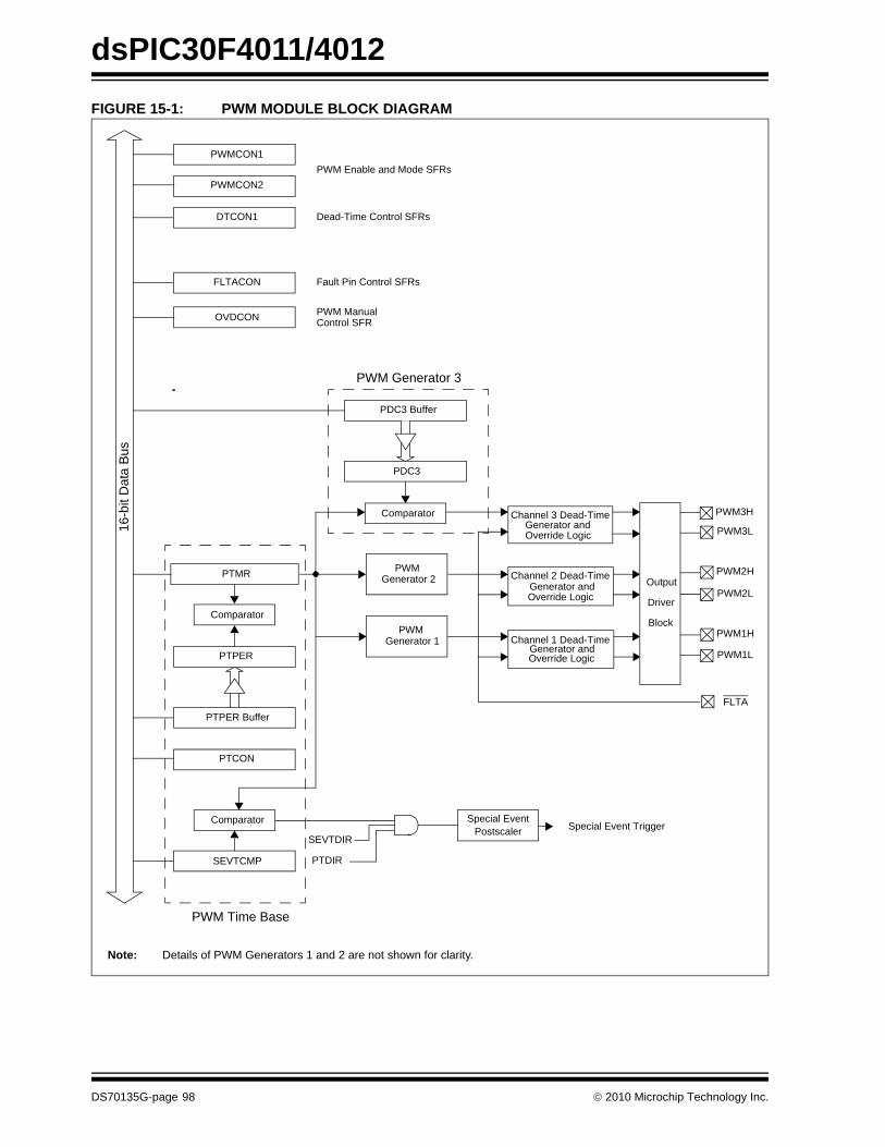
dsPIC30F4011/4012
FIGURE 15-1: PWM MODULE BLOCK DIAGRAMPDC3
PDC3 Buffer
PWMCON1
PWMCON2
PTPER
PTMR
Comparator
Comparator
Channel 3 Dead-TimeGenerator and
PTCON
SEVTCMP
Comparator Special Event Trigger
OVDCON
PWM Enable and Mode SFRs
PWM ManualControl SFR
Channel 2 Dead-TimeGenerator and
Channel 1 Dead-TimeGenerator and
PWM Generator 2
PWM
PWM Generator 3
SEVTDIR
PTDIR
DTCON1 Dead-Time Control SFRs
Special EventPostscaler
PWM1L
PWM1H
PWM2L
PWM2H
Note: Details of PWM Generators 1 and 2 are not shown for clarity.
16-b
it D
ata
Bus
PWM3L
PWM3H
FLTACON Fault Pin Control SFRs
PWM Time Base
Output
Driver
Block
FLTA
Override Logic
Override Logic
Override Logic
PTPER Buffer
Generator 1
DS70135G-page 98 © 2010 Microchip Technology Inc.

dsPIC30F4011/4012
15.1 PWM Time BaseThe PWM time base is provided by a 15-bit timer witha prescaler and postscaler. The time base is accessiblevia the PTMR SFR. PTMR<15> is a read-only statusbit, PTDIR, that indicates the present count direction ofthe PWM time base. If PTDIR is cleared, PTMR iscounting upwards. If PTDIR is set, PTMR is countingdownwards. The PWM time base is configured via thePTCON SFR. The time base is enabled/disabled bysetting/clearing the PTEN bit in the PTCON SFR.PTMR is not cleared when the PTEN bit is cleared insoftware.The PTPER SFR sets the counting period for PTMR.The user must write a 15-bit value to PTPER<14:0>.When the value in PTMR<14:0> matches the value inPTPER<14:0>, the time base will either reset to ‘0’, orreverse the count direction on the next occurring clockcycle. The action taken depends on the operatingmode of the time base.
The PWM time base can be configured for four differentmodes of operation:
• Free-Running mode• Single-Shot mode• Continuous Up/Down Count mode• Continuous Up/Down Count mode with interrupts
for double updates
These four modes are selected by the PTMOD<1:0>bits in the PTCON SFR. The Continuous Up/DownCount modes support center-aligned PWM generation.The Single-Shot mode allows the PWM module to sup-port pulse control of certain Electronically CommutativeMotors (ECMs).
The interrupt signals generated by the PWM time basedepend on the mode selection bits (PTMOD<1:0>) andthe postscaler bits (PTOPS<3:0>) in the PTCON SFR.
15.1.1 FREE-RUNNING MODEIn the Free-Running mode, the PWM time base countsupwards until the value in the Time Base Period regis-ter (PTPER) is matched. The PTMR register is reset onthe following input clock edge and the time base willcontinue to count upwards as long as the PTEN bitremains set.
When the PWM time base is in the Free-Running mode(PTMOD<1:0> = 00), an interrupt event is generatedeach time a match with the PTPER register occurs andthe PTMR register is reset to zero. The postscalerselection bits may be used in this mode of the timer toreduce the frequency of the interrupt events.
15.1.2 SINGLE-SHOT MODEIn the Single-Shot mode, the PWM time base beginscounting upwards when the PTEN bit is set. When thevalue in the PTMR register matches the PTPER regis-ter, the PTMR register will be reset on the followinginput clock edge and the PTEN bit will be cleared by thehardware to halt the time base.
When the PWM time base is in the Single-Shot mode(PTMOD<1:0> = 01), an interrupt event is generatedwhen a match with the PTPER register occurs, thePTMR register is reset to zero on the following inputclock edge and the PTEN bit is cleared. The postscalerselection bits have no effect in this mode of the timer.
15.1.3 CONTINUOUS UP/DOWN COUNT MODES
In the Continuous Up/Down Count modes, the PWMtime base counts upwards until the value in the PTPERregister is matched. The timer will begin countingdownwards on the following input clock edge. ThePTDIR bit in the PTMR SFR is read-only and indicatesthe counting direction. The PTDIR bit is set when thetimer counts downwards.
In the Continuous Up/Down Count mode(PTMOD<1:0> = 10), an interrupt event is generatedeach time the value of the PTMR register becomeszero and the PWM time base begins to count upwards.The postscaler selection bits may be used in this modeof the timer to reduce the frequency of the interruptevents.
Note: If the Period register is set to 0x0000, thetimer will stop counting, and the interruptand special event trigger will not be gener-ated even if the special event value is also0x0000. The module will not update thePeriod register if it is already at 0x0000;therefore, the user must disable themodule in order to update the Periodregister.
© 2010 Microchip Technology Inc. DS70135G-page 99

dsPIC30F4011/4012
15.1.4 DOUBLE UPDATE MODEIn the Double Update mode (PTMOD<1:0> = 11), aninterrupt event is generated each time the PTMR regis-ter is equal to zero, as well as each time a period matchoccurs. The postscaler selection bits have no effect inthis mode of the timer.The Double Update mode provides two additional func-tions to the user. First, the control loop bandwidth isdoubled because the PWM duty cycles can beupdated, twice per period. Second, asymmetricalcenter-aligned PWM waveforms can be generatedwhich are useful for minimizing output waveformdistortion in certain motor control applications.
15.1.5 PWM TIME BASE PRESCALERThe input clock to PTMR (FOSC/4) has prescaleroptions of 1:1, 1:4, 1:16 or 1:64, selected by controlbits, PTCKPS<1:0>, in the PTCON SFR. The prescalercounter is cleared when any of the following occurs:
• A write to the PTMR register• A write to the PTCON register• Any device Reset
The PTMR register is not cleared when PTCON iswritten.
15.1.6 PWM TIME BASE POSTSCALERThe match output of PTMR can optionally be post-scaled through a 4-bit postscaler (which gives a 1:1 to1:16 scaling).
The postscaler counter is cleared when any of thefollowing occurs:
• A write to the PTMR register• A write to the PTCON register• Any device Reset
The PTMR register is not cleared when the PTCONregister is written.
15.2 PWM PeriodPTPER is a 15-bit register and is used to set thecounting period for the PWM time base. PTPER is adouble-buffered register. The PTPER buffer contentsare loaded into the PTPER register at the followinginstants:
• Free-Running and Single-Shot modes: When the PTMR register is reset to zero after a match with the PTPER register.
• Continuous Up/Down Count modes: When the PTMR register is zero.
The value held in the PTPER buffer is automaticallyloaded into the PTPER register when the PWM timebase is disabled (PTEN = 0).
The PWM period can be determined usingEquation 15-1:
EQUATION 15-1: PWM PERIOD
If the PWM time base is configured for one of theContinuous Up/Down Count modes, the PWM period isprovided by Equation 15-2.
EQUATION 15-2: PWM PERIOD (CENTER-ALIGNED MODE)
The maximum resolution (in bits) for a given deviceoscillator and PWM frequency can be determined usingEquation 15-3:
EQUATION 15-3: PWM RESOLUTION
Note: Programming a value of 0x0001 in thePeriod register could generate acontinuous interrupt pulse, and hence,must be avoided.
TPWM = TCY • (PTPER + 1) • PTMR Prescale Value
TPWM = TCY • 2 • PTPER + 1) • PTMR Prescale Value
Resolution =log (2 • TPWM/TCY)
log (2)
DS70135G-page 100 © 2010 Microchip Technology Inc.

dsPIC30F4011/4012
15.3 Edge-Aligned PWM Edge-aligned PWM signals are produced by the modulewhen the PWM time base is in the Free-Running orSingle-Shot mode. For edge-aligned PWM outputs, theoutput has a period specified by the value in PTPERand a duty cycle specified by the appropriate duty cycleregister (see Figure 15-2). The PWM output is drivenactive at the beginning of the period (PTMR = 0) and isdriven inactive when the value in the duty cycle registermatches PTMR.If the value in a particular duty cycle register is zero,then the output on the corresponding PWM pin will beinactive for the entire PWM period. In addition, the out-put on the PWM pin will be active for the entire PWMperiod if the value in the duty cycle register is greaterthan the value held in the PTPER register.
FIGURE 15-2: EDGE-ALIGNED PWM
15.4 Center-Aligned PWMCenter-aligned PWM signals are produced by themodule when the PWM time base is configured in aContinuous Up/Down Count mode (see Figure 15-3).
The PWM compare output is driven to the active statewhen the value of the duty cycle register matches thevalue of PTMR and the PWM time base is countingdownwards (PTDIR = 1). The PWM compare output isdriven to the inactive state when the PWM time base iscounting upwards (PTDIR = 0) and the value in thePTMR register matches the duty cycle value.
If the value in a particular duty cycle register is zero,then the output on the corresponding PWM pin will beinactive for the entire PWM period. In addition, the out-put on the PWM pin will be active for the entire PWMperiod if the value in the duty cycle register is equal tothe value held in the PTPER register.
FIGURE 15-3: CENTER-ALIGNED PWM
Period
Duty Cycle
0
PTPER
PTMRValue
New Duty Cycle Latched
0
PTPER PTMRValue
Period
Period/2
DutyCycle
© 2010 Microchip Technology Inc. DS70135G-page 101

dsPIC30F4011/4012
15.5 PWM Duty Cycle ComparisonUnitsThere are three 16-bit Special Function Registers(PDC1, PDC2 and PDC3) used to specify duty cyclevalues for the PWM module.
The value in each duty cycle register determines theamount of time that the PWM output is in the activestate. The duty cycle registers are 16-bits wide. TheLSb of a duty cycle register determines whether thePWM edge occurs in the beginning. Thus, the PWMresolution is effectively doubled.
15.5.1 DUTY CYCLE REGISTER BUFFERSThe three PWM duty cycle registers are double-buffered to allow glitchless updates of the PWMoutputs. For each duty cycle, there is a duty cycleregister that is accessible by the user and a secondduty cycle register that holds the actual compare valueused in the present PWM period.
For edge-aligned PWM output, a new duty cycle valuewill be updated whenever a match with the PTPER reg-ister occurs and PTMR is reset. The contents of theduty cycle buffers are automatically loaded into theduty cycle registers when the PWM time base is dis-abled (PTEN = 0) and the UDIS bit is cleared inPWMCON2.
When the PWM time base is in the Continuous Up/Down Count mode, new duty cycle values are updatedwhen the value of the PTMR register is zero and thePWM time base begins to count upwards. The contentsof the duty cycle buffers are automatically loaded intothe duty cycle registers when the PWM time base isdisabled (PTEN = 0).
When the PWM time base is in the Continuous Up/Down Count mode with double updates, new duty cyclevalues are updated when the value of the PTMR regis-ter is zero, and when the value of the PTMR registermatches the value in the PTPER register. The contentsof the duty cycle buffers are automatically loaded intothe duty cycle registers when the PWM time base isdisabled (PTEN = 0).
15.6 Complementary PWM OperationIn the Complementary mode of operation, each pair ofPWM outputs is obtained by a complementary PWMsignal. A dead time may be optionally inserted duringdevice switching when both outputs are inactive fora short period (refer to Section 15.7 “Dead-TimeGenerators”).
In Complementary mode, the duty cycle comparisonunits are assigned to the PWM outputs as follows:
• PDC1 register controls PWM1H/PWM1L outputs• PDC2 register controls PWM2H/PWM2L outputs• PDC3 register controls PWM3H/PWM3L outputs
The Complementary mode is selected for each PWMI/O pin pair by clearing the appropriate PTMODx bit inthe PWMCON1 SFR. The PWM I/O pins are set toComplementary mode by default upon a device Reset.
15.7 Dead-Time GeneratorsDead-time generation may be provided when any ofthe PWM I/O pin pairs are operating in theComplementary Output mode. The PWM outputs usepush-pull drive circuits. Due to the inability of the poweroutput devices to switch instantaneously, some amountof time must be provided between the turn-off eventof one PWM output in a complementary pair and theturn-on event of the other transistor.
The PWM module allows two different dead times to beprogrammed. These two dead times may be used inone of two methods described below to increase userflexibility:
• The PWM output signals can be optimized for different turn-off times in the high side and low side transistors in a complementary pair of tran-sistors. The first dead time is inserted between the turn-off event of the lower transistor of the complementary pair and the turn-on event of the upper transistor. The second dead time is inserted between the turn-off event of the upper transistor and the turn-on event of the lower transistor.
• The two dead times can be assigned to individual PWM I/O pin pairs. This operating mode allows the PWM module to drive different transistor/load combinations with each complementary PWM I/O pin pair.
DS70135G-page 102 © 2010 Microchip Technology Inc.

dsPIC30F4011/4012
15.7.1 DEAD-TIME GENERATORSEach complementary output pair for the PWM modulehas a 6-bit down counter that is used to produce thedead-time insertion. As shown in Figure 15-4, eachdead-time unit has a rising and falling edge detectorconnected to the duty cycle comparison output.15.7.2 DEAD-TIME RANGESThe amount of dead time provided by the dead-timeunit is selected by specifying the input clock prescalervalue and a 6-bit unsigned value.
Four input clock prescaler selections have beenprovided to allow a suitable range of dead time basedon the device operating frequency. The dead-timeclock prescaler values are selected using the
DTAPS<1:0> control bits in the DTCON1 SFR. One offour clock prescaler options (TCY, 2 TCY, 4 TCY or 8 TCY)may be selected.
After the prescaler value is selected, the dead time isadjusted by loading 6-bit unsigned values into theDTCON1 SFR.
The dead-time unit prescaler is cleared on the followingevents:
• On a load of the down timer due to a duty cycle comparison edge event.
• On a write to the DTCON1 register.• On any device Reset.
FIGURE 15-4: DEAD-TIME TIMING DIAGRAM
Note: The user should not modify the DTCON1register value while the PWM module isoperating (PTEN = 1). Unexpected resultsmay occur.
Duty Cycle Generator
PWMxH
PWMxL
Dead-Time A (Active) Dead-Time A (Inactive)
© 2010 Microchip Technology Inc. DS70135G-page 103

dsPIC30F4011/4012
15.8 Independent PWM OutputAn Independent PWM Output mode is required fordriving certain types of loads. A particular PWM outputpair is in the Independent Output mode when thecorresponding PTMODx bit in the PWMCON1 registeris set. No dead-time control is implemented betweenadjacent PWM I/O pins when the module is operatingin the Independent Output mode and both I/O pins areallowed to be active simultaneously.In the Independent Output mode, each duty cyclegenerator is connected to both of the PWM I/O pins inan output pair. By using the associated duty cycle reg-ister and the appropriate bits in the OVDCON register,the user may select the following signal output optionsfor each PWM I/O pin operating in the IndependentOutput mode:
• I/O pin outputs PWM signal• I/O pin inactive• I/O pin active
15.9 Single Pulse PWM OperationThe PWM module produces single pulse outputs whenthe PTCON control bits, PTMOD<1:0> = 10. Onlyedge-aligned outputs may be produced in the SinglePulse mode. In Single Pulse mode, the PWM I/O pin(s)are driven to the active state when the PTEN bit is set.When a match with a duty cycle register occurs, thePWM I/O pin is driven to the inactive state. When amatch with the PTPER register occurs, the PTMR reg-ister is cleared, all active PWM I/O pins are driven tothe inactive state, the PTEN bit is cleared and aninterrupt is generated.
15.10 PWM Output OverrideThe PWM output override bits allow the user to manu-ally drive the PWM I/O pins to specified logic states,independent of the duty cycle comparison units.
All control bits associated with the PWM output over-ride function are contained in the OVDCON register.The upper half of the OVDCON register contains sixbits, POVDxH<3:1> and POVDxL<3:1>, that determinewhich PWM I/O pins will be overridden. The lower halfof the OVDCON register contains six bits,POUTxH<3:1> and POUTxL<3:1>, that determine thestate of the PWM I/O pins when a particular output isoverridden via the POVD bits.
15.10.1 COMPLEMENTARY OUTPUT MODEWhen a PWMxL pin is driven active via the OVDCONregister, the output signal is forced to be the comple-ment of the corresponding PWMxH pin in the pair.Dead-time insertion is still performed when PWMchannels are overridden manually.
15.10.2 OVERRIDE SYNCHRONIZATIONIf the OSYNC bit in the PWMCON2 register is set, alloutput overrides performed via the OVDCON registerare synchronized to the PWM time base. Synchronousoutput overrides occur at the following times:
• Edge-Aligned mode when PTMR is zero.• Center-Aligned modes when PTMR is zero and
when the value of PTMR matches PTPER.
DS70135G-page 104 © 2010 Microchip Technology Inc.

dsPIC30F4011/4012
15.11 PWM Output and Polarity ControlThere are three device Configuration bits associatedwith the PWM module that provide PWM output pincontrol:• HPOL Configuration bit• LPOL Configuration bit• PWMPIN Configuration bit
These three bits in the FBORPOR Configuration regis-ter (see Section 21.0 “System Integration”) work inconjunction with the six PWM Enable bits (PENxL andPENxH). The Configuration bits and PWM Enable bitsensure that the PWM pins are in the correct states aftera device Reset occurs. The PWMPIN Configurationfuse allows the PWM module outputs to be optionallyenabled on a device Reset. If PWMPIN = 0, the PWMoutputs will be driven to their inactive states at Reset. IfPWMPIN = 1 (default), the PWM outputs will be tri-stated. The HPOL bit specifies the polarity for thePWMxH outputs, whereas the LPOL bit specifies thepolarity for the PWMxL outputs.
15.11.1 OUTPUT PIN CONTROLThe PENxH<3:1> and PENxL<3:1> control bits in thePWMCON1 SFR enable each high PWM output pinand each low PWM output pin, respectively. If aparticular PWM output pin is not enabled, it is treatedas a general purpose I/O pin.
15.12 PWM Fault PinThere is one Fault pin (FLTA) associated with the PWMmodule. When asserted, this pin can optionally driveeach of the PWM I/O pins to a defined state.
15.12.1 FAULT PIN ENABLE BITSThe FLTACON SFR has three control bits that deter-mine whether a particular pair of PWM I/O pins is to becontrolled by the Fault input pin. To enable aspecific PWM I/O pin pair for Fault overrides, thecorresponding bit should be set in the FLTACONregister.
If all enable bits are cleared in the FLTACON register,then the corresponding Fault input pin has no effect onthe PWM module and the pin may be used as a generalpurpose interrupt or I/O pin.
15.12.2 FAULT STATESThe FLTACON Special Function Register has six bitsthat determine the state of each PWM I/O pin when it isoverridden by a Fault input. When these bits arecleared, the PWM I/O pin is driven to the inactive state.If the bit is set, the PWM I/O pin will be driven to theactive state. The active and inactive states are refer-enced to the polarity defined for each PWM I/O pin(HPOL and LPOL polarity control bits).
A special case exists when a PWM module I/O pair isin the Complementary mode and both pins areprogrammed to be active on a Fault condition. ThePWMxH pin always has priority in the Complementarymode, so that both I/O pins cannot be driven activesimultaneously.
15.12.3 FAULT INPUT MODESThe Fault input pin has two modes of operation:
• Latched Mode: When the Fault pin is driven low, the PWM outputs will go to the states defined in the FLTACON register. The PWM outputs will remain in this state until the Fault pin is driven high and the corresponding interrupt flag has been cleared in software. When both of these actions have occurred, the PWM outputs will return to normal operation at the beginning of the next PWM cycle or half-cycle boundary. If the interrupt flag is cleared before the Fault condition ends, the PWM module will wait until the Fault pin is no longer asserted to restore the outputs.
• Cycle-by-Cycle Mode: When the Fault input pin is driven low, the PWM outputs remain in the defined Fault states for as long as the Fault pin is held low. After the Fault pin is driven high, the PWM outputs return to normal operation at the beginning of the following PWM cycle or half-cycle boundary.
The operating mode for the Fault input pin is selectedusing the FLTAM control bit in the FLTACON SpecialFunction Register.
The Fault pin can be controlled manually in software.
Note: The Fault pin logic can operate indepen-dent of the PWM logic. If all the enable bitsin the FLTACON register are cleared, thenthe Fault pin could be used as a generalpurpose interrupt pin. The Fault pin has aninterrupt vector, interrupt flag bit andinterrupt priority bits associated with it.
© 2010 Microchip Technology Inc. DS70135G-page 105
dsPIC30F4011/4012
15.13 PWM Update LockoutFor a complex PWM application, the user may need towrite up to three duty cycle registers and the Time BasePeriod register, PTPER, at a given time. In some appli-cations, it is important that all buffer registers be writtenbefore the new duty cycle and period values are loadedfor use by the module.The PWM update lockout feature is enabled by settingthe UDIS control bit in the PWMCON2 SFR. The UDISbit affects all duty cycle buffer registers and the PWMTime Base Period buffer, PTPER. No duty cyclechanges or period value changes will have effect whileUDIS = 1.
15.14 PWM Special Event TriggerThe PWM module has a special event trigger thatallows A/D conversions to be synchronized to the PWMtime base. The A/D sampling and conversion time maybe programmed to occur at any point within the PWMperiod. The special event trigger allows the user to min-imize the delay between the time when A/D conversionresults are acquired and the time when the duty cyclevalue is updated.
The PWM special event trigger has an SFR namedSEVTCMP and five control bits to control its operation.The PTMR value for which a special event triggershould occur is loaded into the SEVTCMP register.When the PWM time base is in a Continuous Up/DownCount mode, an additional control bit is required tospecify the counting phase for the special event trigger.The count phase is selected using the SEVTDIR con-trol bit in the SEVTCMP SFR. If the SEVTDIR bit iscleared, the special event trigger will occur on theupward counting cycle of the PWM time base. If theSEVTDIR bit is set, the special event trigger will occuron the downward count cycle of the PWM time base.The SEVTDIR control bit has no effect unless the PWMtime base is configured for a Continuous Up/DownCount mode.
15.14.1 SPECIAL EVENT TRIGGER POSTSCALER
The PWM special event trigger has a postscaler thatallows a 1:1 to 1:16 postscale ratio. The postscaler isconfigured by writing the SEVOPS<3:0> control bits inthe PWMCON2 SFR.
The special event output postscaler is cleared on thefollowing events:
• Any write to the SEVTCMP register• Any device Reset
15.15 PWM Operation During CPU Sleep Mode
The Fault A input pin has the ability to wake the CPUfrom Sleep mode. The PWM module generates aninterrupt if the Fault pin is driven low while in Sleep.
15.16 PWM Operation During CPU Idle Mode
The PTCON SFR contains a PTSIDL control bit. Thisbit determines if the PWM module will continue tooperate or stop when the device enters Idle mode. IfPTSIDL = 0, the module will continue to operate. IfPTSIDL = 1, the module will stop operation as long asthe CPU remains in Idle mode.
DS70135G-page 106 © 2010 Microchip Technology Inc.

© 2010 M
icrochip Technology Inc.D
S70135G
-page 107
dsPIC30F4011/4012
TASF 2 Bit 1 Bit 0 Reset State
PT PTMOD<1:0> 0000 0000 0000 0000
PT 0000 0000 0000 0000
PT 0111 1111 1111 1111
SE 0000 0000 0000 0000
PW 3L PEN2L PEN1L 0000 0000 1111 1111
PW OSYNC UDIS 0000 0000 0000 0000
DT lue 0000 0000 0000 0000
FL 3 FAEN2 FAEN1 0000 0000 0000 0000
OV 2L POUT1H POUT1L 1111 1111 0000 0000
PD 0000 0000 0000 0000
PD 0000 0000 0000 0000
PD 0000 0000 0000 0000
LeNo
BLE 15-1: 6-OUTPUT PWM REGISTER MAP(1)
R Name Addr. Bit 15 Bit 14 Bit 13 Bit 12 Bit 11 Bit 10 Bit 9 Bit 8 Bit 7 Bit 6 Bit 5 Bit 4 Bit 3 Bit
CON 01C0 PTEN — PTSIDL — — — — — PTOPS<3:0> PTCKPS<1:0>
MR 01C2 PTDIR PWM Timer Count Value
PER 01C4 — PWM Time Base Period Register
VTCMP 01C6 SEVTDIR PWM Special Event Compare Register
MCON1 01C8 — — — — — PTMOD3 PTMOD2 PTMOD1 — PEN3H PEN2H PEN1H — PEN
MCON2 01CA — — — — SEVOPS<3:0> — — — — — IUE
CON1 01CC — — — — — — — — DTAPS<1:0> Dead-Time A Va
TACON 01D0 — — FAOV3H FAOV3L FAOV2H FAOV2L FAOV1H FAOV1L FLTAM — — — — FAEN
DCON 01D4 — — POVD3H POVD3L POVD2H POVD2L POVD1H POVD1L — — POUT3H POUT3L POUT2H POUT
C1 01D6 PWM Duty Cycle 1 Register
C2 01D8 PWM Duty Cycle 2 Register
C3 01DA PWM Duty Cycle 3 Register
gend: — = unimplemented bit, read as ‘0’te 1: Refer to the “dsPIC30F Family Reference Manual” (DS70046) for descriptions of register bit fields.

dsPIC30F4011/4012
NOTES:DS70135G-page 108 © 2010 Microchip Technology Inc.
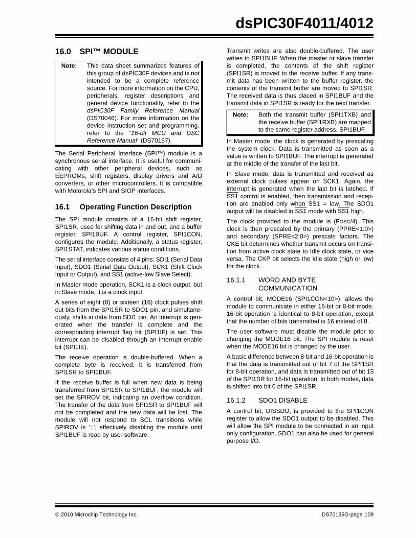
dsPIC30F4011/4012
16.0 SPI™ MODULE
The Serial Peripheral Interface (SPI™) module is asynchronous serial interface. It is useful for communi-cating with other peripheral devices, such asEEPROMs, shift registers, display drivers and A/Dconverters, or other microcontrollers. It is compatiblewith Motorola’s SPI and SIOP interfaces.
16.1 Operating Function DescriptionThe SPI module consists of a 16-bit shift register,SPI1SR, used for shifting data in and out, and a bufferregister, SPI1BUF. A control register, SPI1CON,configures the module. Additionally, a status register,SPI1STAT, indicates various status conditions.
The serial interface consists of 4 pins: SDI1 (Serial DataInput), SDO1 (Serial Data Output), SCK1 (Shift ClockInput or Output), and SS1 (active-low Slave Select).
In Master mode operation, SCK1 is a clock output, butin Slave mode, it is a clock input.
A series of eight (8) or sixteen (16) clock pulses shiftout bits from the SPI1SR to SDO1 pin, and simultane-ously, shifts in data from SDI1 pin. An interrupt is gen-erated when the transfer is complete and thecorresponding interrupt flag bit (SPI1IF) is set. Thisinterrupt can be disabled through an interrupt enablebit (SPI1IE).
The receive operation is double-buffered. When acomplete byte is received, it is transferred fromSPI1SR to SPI1BUF.
If the receive buffer is full when new data is beingtransferred from SPI1SR to SPI1BUF, the module willset the SPIROV bit, indicating an overflow condition.The transfer of the data from SPI1SR to SPI1BUF willnot be completed and the new data will be lost. Themodule will not respond to SCL transitions whileSPIROV is ‘1’, effectively disabling the module untilSPI1BUF is read by user software.
Transmit writes are also double-buffered. The userwrites to SPI1BUF. When the master or slave transferis completed, the contents of the shift register(SPI1SR) is moved to the receive buffer. If any trans-mit data has been written to the buffer register, thecontents of the transmit buffer are moved to SPI1SR.The received data is thus placed in SPI1BUF and thetransmit data in SPI1SR is ready for the next transfer.
In Master mode, the clock is generated by prescalingthe system clock. Data is transmitted as soon as avalue is written to SPI1BUF. The interrupt is generatedat the middle of the transfer of the last bit.
In Slave mode, data is transmitted and received asexternal clock pulses appear on SCK1. Again, theinterrupt is generated when the last bit is latched. IfSS1 control is enabled, then transmission and recep-tion are enabled only when SS1 = low. The SDO1output will be disabled in SS1 mode with SS1 high.
The clock provided to the module is (FOSC/4). Thisclock is then prescaled by the primary (PPRE<1:0>)and secondary (SPRE<2:0>) prescale factors. TheCKE bit determines whether transmit occurs on transi-tion from active clock state to Idle clock state, or viceversa. The CKP bit selects the Idle state (high or low)for the clock.
16.1.1 WORD AND BYTE COMMUNICATION
A control bit, MODE16 (SPI1CON<10>), allows themodule to communicate in either 16-bit or 8-bit mode.16-bit operation is identical to 8-bit operation, exceptthat the number of bits transmitted is 16 instead of 8.
The user software must disable the module prior tochanging the MODE16 bit. The SPI module is resetwhen the MODE16 bit is changed by the user.
A basic difference between 8-bit and 16-bit operation isthat the data is transmitted out of bit 7 of the SPI1SRfor 8-bit operation, and data is transmitted out of bit 15of the SPI1SR for 16-bit operation. In both modes, datais shifted into bit 0 of the SPI1SR.
16.1.2 SDO1 DISABLEA control bit, DISSDO, is provided to the SPI1CONregister to allow the SDO1 output to be disabled. Thiswill allow the SPI module to be connected in an inputonly configuration. SDO1 can also be used for generalpurpose I/O.
Note: This data sheet summarizes features ofthis group of dsPIC30F devices and is notintended to be a complete referencesource. For more information on the CPU,peripherals, register descriptions andgeneral device functionality, refer to thedsPIC30F Family Reference Manual(DS70046). For more information on thedevice instruction set and programming,refer to the “16-bit MCU and DSCReference Manual” (DS70157).
Note: Both the transmit buffer (SPI1TXB) andthe receive buffer (SPI1RXB) are mappedto the same register address, SPI1BUF.
© 2010 Microchip Technology Inc. DS70135G-page 109
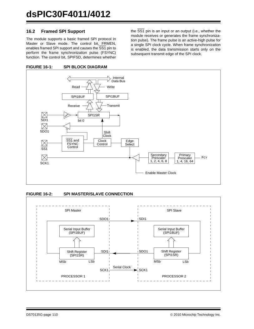
dsPIC30F4011/4012
16.2 Framed SPI SupportThe module supports a basic framed SPI protocol inMaster or Slave mode. The control bit, FRMEN,enables framed SPI support and causes the SS1 pin toperform the frame synchronization pulse (FSYNC)function. The control bit, SPIFSD, determines whetherthe SS1 pin is an input or an output (i.e., whether themodule receives or generates the frame synchroniza-tion pulse). The frame pulse is an active-high pulse fora single SPI clock cycle. When frame synchronizationis enabled, the data transmission starts only on thesubsequent transmit edge of the SPI clock.
FIGURE 16-1: SPI BLOCK DIAGRAM
FIGURE 16-2: SPI MASTER/SLAVE CONNECTION
Read Write
InternalData Bus
SDI1
SDO1
SS1
SCK1
SPI1SR
SPI1BUF
bit 0
ShiftClock
EdgeSelect
FCYPrimary
1, 4, 16, 64
Enable Master Clock
PrescalerSecondaryPrescaler
1, 2, 4, 6, 8
Transmit
SPI1BUF
Receive
SS1 and
Control
ClockControlFSYNC
Serial Input Buffer(SPI1BUF)
Shift Register(SPI1SR)
MSb LSb
SDO1
SDI1
PROCESSOR 1
SCK1
SPI Master
Serial Input Buffer(SPI1BUF)
LSbMSb
SDI1
SDO1
PROCESSOR 2
SCK1
SPI Slave
Serial Clock
Shift Register(SPI1SR)
DS70135G-page 110 © 2010 Microchip Technology Inc.

dsPIC30F4011/4012
16.3 Slave Select SynchronizationThe SS1 pin allows a Synchronous Slave mode. TheSPI must be configured in SPI Slave mode, with SS1pin control enabled (SSEN = 1). When the SS1 pin islow, transmission and reception are enabled and theSDO1 pin is driven. When SS1 pin goes high, theSDO1 pin is no longer driven. Also, the SPI module isresynchronized and all counters/control circuitry arereset. Therefore, when the SS1 pin is asserted lowagain, transmission/reception will begin at the MSb,even if SS1 had been deasserted in the middle of atransmit/receive.16.4 SPI Operation During CPU Sleep Mode
During Sleep mode, the SPI module is shut down. Ifthe CPU enters Sleep mode while an SPI transactionis in progress, then the transmission and reception isaborted.
The transmitter and receiver will stop in Sleep mode.However, register contents are not affected byentering or exiting Sleep mode.
16.5 SPI Operation During CPU Idle Mode
When the device enters Idle mode, all clock sourcesremain functional. The SPISIDL bit (SPI1STAT<13>)selects if the SPI module will stop or continue on Idle.If SPISIDL = 0, the module will continue to operatewhen the CPU enters Idle mode. If SPISIDL = 1, themodule will stop when the CPU enters Idle mode.
© 2010 Microchip Technology Inc. DS70135G-page 111

dsPIC30F4011/4012
DS
70135G-page 112
© 2010 M
icrochip Technology Inc.
Bit 2 Bit 1 Bit 0 Reset State
— SPITBF SPIRBF 0000 0000 0000 0000
SPRE0 PPRE1 PPRE0 0000 0000 0000 0000
0000 0000 0000 0000
TABLE 16-1: SPI1 REGISTER MAP(1)
SFR Name Addr. Bit 15 Bit 14 Bit 13 Bit 12 Bit 11 Bit 10 Bit 9 Bit 8 Bit 7 Bit 6 Bit 5 Bit 4 Bit 3
SPI1STAT 0220 SPIEN — SPISIDL — — — — — — SPIROV — — —
SPI1CON 0222 — FRMEN SPIFSD — DISSDO MODE16 SMP CKE SSEN CKP MSTEN SPRE2 SPRE1
SPI1BUF 0224 Transmit and Receive Buffer
Legend: u = uninitialized bit; — = unimplemented bit, read as ‘0’Note 1: Refer to the “dsPIC30F Family Reference Manual” (DS70046) for descriptions of register bit fields.

dsPIC30F4011/4012
17.0 I2C™ MODULE
The Inter-Integrated Circuit (I2C™) module providescomplete hardware support for both Slave and Multi-Master modes of the I2C serial communicationstandard with a 16-bit interface.
This module offers the following key features:
• I2C Interface supporting both Master and Slave Operation
• I2C Slave mode supports 7-bit and 10-bit address-ing
• I2C Master mode supports 7-bit and 10-bit addressing
• I2C Port allows Bidirectional Transfers between Master and Slaves
• Serial Clock Synchronization for I2C Port can be used as a Handshake Mechanism to Suspend and Resume Serial Transfer (SCLREL control)
• I2C supports Multi-Master Operation; detects bus collision and will arbitrate accordingly
17.1 Operating Function DescriptionThe hardware fully implements all the master and slavefunctions of the I2C Standard and Fast modespecifications, as well as 7 and 10-bit addressing.
Thus, the I2C module can operate either as a slave ora master on an I2C bus.
17.1.1 VARIOUS I2C MODESThe following types of I2C operation are supported:
• I2C slave operation with 7-bit addressing• I2C slave operation with 10-bit addressing• I2C master operation with 7-bit or 10-bit addressing
See the I2C programmer’s model in Figure 17-1.
17.1.2 PIN CONFIGURATION IN I2C MODEI2C has a 2-pin interface. The SCL pin is clock and theSDA pin is data.
17.1.3 I2C REGISTERSI2CCON and I2CSTAT are control and status registers,respectively. The I2CCON register is readable and writ-able. The lower 6 bits of I2CSTAT are read-only. Theremaining bits of the I2CSTAT are read/write.
I2CRSR is the shift register used for shifting data,whereas I2CRCV is the buffer register to which databytes are written or from which data bytes are read.I2CRCV is the receive buffer, as shown in Figure 17-1.I2CTRN is the transmit register to which bytes arewritten during a transmit operation, as shown inFigure 17-2.
The I2CADD register holds the slave address. A statusbit, ADD10, indicates 10-bit Address mode. TheI2CBRG acts as the Baud Rate Generator reloadvalue.
In receive operations, I2CRSR and I2CRCV togetherform a double-buffered receiver. When I2CRSRreceives a complete byte, it is transferred to I2CRCVand an interrupt pulse is generated. Duringtransmission, the I2CTRN is not double-buffered.
FIGURE 17-1: PROGRAMMER’S MODEL
Note: This data sheet summarizes features ofthis group of dsPIC30F devices and is notintended to be a complete referencesource. For more information on the CPU,peripherals, register descriptions andgeneral device functionality, refer to thedsPIC30F Family Reference Manual(DS70046). For more information on thedevice instruction set and programming,refer to the “16-bit MCU and DSCReference Manual” (DS70157).
Note: Following a Restart condition in 10-bitmode, the user only needs to match thefirst 7-bit address.
bit 7 bit 0I2CRCV (8 bits)
bit 7 bit 0I2CTRN (8 bits)
bit 8 bit 0I2CBRG (9 bits)
bit 15 bit 0I2CCON (16-bits)
bit 15 bit 0I2CSTAT (16-bits)
bit 9 bit 0I2CADD (10-bits)
© 2010 Microchip Technology Inc. DS70135G-page 113

dsPIC30F4011/4012
FIGURE 17-2: I2C™ BLOCK DIAGRAMI2CRSR
I2CRCV
InternalData Bus
SCL
SDA
Shift
Match Detect
I2CADD
Start andStop bit Detect
Clock
Addr_Match
ClockStretching
I2CTRNLSBShift
Clock
Write
ReadBRG Down I2CBRG
ReloadControl
FCY
Start, Restart,Stop bit Generate
Write
Read
AcknowledgeGeneration
CollisionDetect
Write
Read
Write
ReadI2C
CO
N
Write
ReadI2C
STA
T
Con
trol L
ogic
Read
LSB
Counter
DS70135G-page 114 © 2010 Microchip Technology Inc.

dsPIC30F4011/4012
17.2 I2C Module AddressesThe I2CADD register contains the Slave modeaddresses. The register is a 10-bit register.If the A10M bit (I2CCON<10>) is ‘0’, the address isinterpreted by the module as a 7-bit address. When anaddress is received, it is compared to the 7 LSbs of theI2CADD register.
If the A10M bit is ‘1’, the address is assumed to be a10-bit address. When an address is received, it will becompared with the binary value, ‘11110 A9 A8’(where A9 and A8 are two Most Significant bits ofI2CADD). If that value matches, the next address willbe compared with the Least Significant 8 bits ofI2CADD, as specified in the 10-bit addressing protocol.
The 7-bit I2C slave addresses supported by thedsPIC30F are shown in Table 17-1.
TABLE 17-1: 7-BIT I2C™ SLAVE ADDRESSES
17.3 I2C 7-bit Slave Mode OperationOnce enabled (I2CEN = 1), the slave module will waitfor a Start bit to occur (i.e., the I2C module is ‘Idle’).Following the detection of a Start bit, 8 bits are shiftedinto I2CRSR and the address is compared againstI2CADD. In 7-bit mode (A10M = 0), I2CADD<6:0> bitsare compared against I2CRSR<7:1>, and I2CRSR<0>is the R_W bit. All incoming bits are sampled on therising edge of SCL.
If an address match occurs, an Acknowledgement willbe sent, and the Slave Event Interrupt Flag (SI2CIF) isset on the falling edge of the ninth (ACK) bit. Theaddress match does not affect the contents of theI2CRCV buffer or the RBF bit.
17.3.1 SLAVE TRANSMISSIONIf the R_W bit received is a ‘1’, then the serial port willgo into Transmit mode. It will send ACK on the ninth bitand then hold SCL to ‘0’ until the CPU responds by writ-ing to I2CTRN. SCL is released by setting the SCLRELbit and 8 bits of data are shifted out. Data bits areshifted out on the falling edge of SCL, such that SDA isvalid during SCL high (see timing diagram). The inter-rupt pulse is sent on the falling edge of the ninth clockpulse, regardless of the status of the ACK receivedfrom the master.
17.3.2 SLAVE RECEPTIONIf the R_W bit received is a ‘0’ during an addressmatch, then Receive mode is initiated. Incoming bitsare sampled on the rising edge of SCL. After 8 bits arereceived, if I2CRCV is not full or I2COV is not set,I2CRSR is transferred to I2CRCV. ACK is sent on theninth clock.
If the RBF flag is set, indicating that I2CRCV is stillholding data from a previous operation (RBF = 1), thenACK is not sent; however, the interrupt pulse is gener-ated. In the case of an overflow, the contents of theI2CRSR are not loaded into the I2CRCV.
17.4 I2C 10-bit Slave Mode OperationIn 10-bit mode, the basic receive and transmitoperations are the same as in the 7-bit mode. However,the criteria for address match is more complex.
The I2C specification dictates that a slave must beaddressed for a write operation, with two address bytesfollowing a Start bit.
The A10M bit is a control bit that signifies that theaddress in I2CADD is a 10-bit address rather than a7-bit address. The address detection protocol for thefirst byte of a message address is identical for 7-bitand 10-bit messages but the bits being compared aredifferent.
I2CADD holds the entire 10-bit address. Upon receiv-ing an address following a Start bit, I2CRSR<7:3> iscompared against a literal ‘11110’ (the default 10-bitaddress) and I2CRSR<2:1> are compared againstI2CADD<9:8>. If a match occurs and if R_W = 0, theinterrupt pulse is sent. The ADD10 bit will be cleared toindicate a partial address match. If a match fails orR_W = 1, the ADD10 bit is cleared and the modulereturns to the Idle state.
The low byte of the address is then received and com-pared with I2CADD<7:0>. If an address match occurs,the interrupt pulse is generated and the ADD10 bit isset, indicating a complete 10-bit address match. If anaddress match did not occur, the ADD10 bit is clearedand the module returns to the Idle state.
Address Description
0x00 General call address or Start byte0x01-0x03 Reserved0x04-0x07 HS mode master codes0x08-0x77 Valid 7-bit addresses0x78-0x7B Valid 10-bit addresses (lower 7 bits)0x7C-0x7F Reserved
Note: The I2CRCV will be loaded if the I2COVbit = 1 and the RBF flag = 0. In this case,a read of the I2CRCV was performed butthe user did not clear the state of theI2COV bit before the next receiveoccurred. The Acknowledgement is notsent (ACK = 1) and the I2CRCV isupdated.
© 2010 Microchip Technology Inc. DS70135G-page 115

dsPIC30F4011/4012
17.4.1 10-BIT MODE SLAVETRANSMISSIONOnce a slave is addressed in this fashion, with the full10-bit address (we will refer to this state as“PRIOR_ADDR_MATCH”), the master can beginsending data bytes for a slave reception operation.
17.4.2 10-BIT MODE SLAVE RECEPTIONOnce addressed, the master can generate a RepeatedStart, reset the high byte of the address and set theR_W bit without generating a Stop bit, thus initiating aslave transmit operation.
17.5 Automatic Clock StretchIn the Slave modes, the module can synchronize bufferreads and write to the master device by clock stretching.
17.5.1 TRANSMIT CLOCK STRETCHINGBoth 10-bit and 7-bit Transmit modes implement clockstretching by asserting the SCLREL bit after the fallingedge of the ninth clock if the TBF bit is cleared,indicating the buffer is empty.
In Slave Transmit modes, clock stretching is alwaysperformed, irrespective of the STREN bit.
Clock synchronization takes place following the ninthclock of the transmit sequence. If the device samplesan ACK on the falling edge of the ninth clock, and if theTBF bit is still clear, then the SCLREL bit is automati-cally cleared. The SCLREL being cleared to ‘0’ willassert the SCL line low. The user’s ISR must set theSCLREL bit before transmission is allowed tocontinue. By holding the SCL line low, the user hastime to service the ISR and load the contents of theI2CTRN before the master device can initiate anothertransmit sequence.
17.5.2 RECEIVE CLOCK STRETCHINGThe STREN bit in the I2CCON register can be used toenable clock stretching in Slave Receive mode. Whenthe STREN bit is set, the SCL pin will be held low atthe end of each data receive sequence.
17.5.3 CLOCK STRETCHING DURING 7-BIT ADDRESSING (STREN = 1)
When the STREN bit is set in Slave Receive mode,the SCL line is held low when the buffer register is full.The method for stretching the SCL output is the samefor both 7-bit and 10-bit Addressing modes.
Clock stretching takes place following the ninth clock ofthe receive sequence. On the falling edge of the ninthclock at the end of the ACK sequence, if the RBF bit isset, the SCLREL bit is automatically cleared, forcing theSCL output to be held low. The user’s ISR must set theSCLREL bit before reception is allowed to continue. Byholding the SCL line low, the user has time to servicethe ISR and read the contents of the I2CRCV before themaster device can initiate another receive sequence.This will prevent buffer overruns from occurring.
17.5.4 CLOCK STRETCHING DURING 10-BIT ADDRESSING (STREN = 1)
Clock stretching takes place automatically during theaddressing sequence. Because this module has aregister for the entire address, it is not necessary forthe protocol to wait for the address to be updated.
After the address phase is complete, clock stretchingwill occur on each data receive or transmit sequenceas was described earlier.
17.6 Software Controlled Clock Stretching (STREN = 1)
When the STREN bit is ‘1’, the SCLREL bit may becleared by software to allow software to control theclock stretching. The logic will synchronize writes tothe SCLREL bit with the SCL clock. Clearing theSCLREL bit will not assert the SCL output until themodule detects a falling edge on the SCL output andSCL is sampled low. If the SCLREL bit is cleared bythe user while the SCL line has been sampled low, theSCL output will be asserted (held low). The SCL out-put will remain low until the SCLREL bit is set and allother devices on the I2C bus have deasserted SCL.This ensures that a write to the SCLREL bit will notviolate the minimum high time requirement for SCL.
If the STREN bit is ‘0’, a software write to the SCLRELbit will be disregarded and have no effect on theSCLREL bit.
Note 1: If the user loads the contents of I2CTRN,setting the TBF bit before the falling edgeof the ninth clock, the SCLREL bit will notbe cleared and clock stretching will notoccur.
2: The SCLREL bit can be set in softwareregardless of the state of the TBF bit.
Note 1: If the user reads the contents of theI2CRCV, clearing the RBF bit before thefalling edge of the ninth clock, theSCLREL bit will not be cleared and clockstretching will not occur.
2: The SCLREL bit can be set in software,regardless of the state of the RBF bit. Theuser should be careful to clear the RBFbit in the ISR before the next receivesequence in order to prevent an overflowcondition.
DS70135G-page 116 © 2010 Microchip Technology Inc.

dsPIC30F4011/4012
17.7 InterruptsThe I2C module generates two interrupt flags, MI2CIF(I2C Master Interrupt Flag) and SI2CIF (I2C Slave Inter-rupt Flag). The MI2CIF interrupt flag is activated oncompletion of a master message event. The SI2CIFinterrupt flag is activated on detection of a messagedirected to the slave.17.8 Slope ControlThe I2C standard requires slope control on the SDAand SCL signals for Fast mode (400 kHz). The controlbit, DISSLW, enables the user to disable slew rate con-trol, if desired. It is necessary to disable the slew ratecontrol for 1 MHz mode.
17.9 IPMI SupportThe control bit, IPMIEN, enables the module to supportIntelligent Peripheral Management Interface (IPMI).When this bit is set, the module accepts and acts uponall addresses.
17.10 General Call Address SupportThe general call address can address all devices.When this address is used, all devices should, intheory, respond with an Acknowledgement.
The general call address is one of eight addressesreserved for specific purposes by the I2C protocol. Itconsists of all ‘0’s with R_W = 0.
The general call address is recognized when the Gen-eral Call Enable (GCEN) bit is set (I2CCON<7> = 1).Following a Start bit detection, 8 bits are shifted intoI2CRSR and the address is compared with I2CADD,and is also compared with the general call addresswhich is fixed in hardware.
If a general call address match occurs, the I2CRSR istransferred to the I2CRCV after the eighth clock, theRBF flag is set, and on the falling edge of the ninth bit(ACK bit), the Master Event Interrupt Flag (MI2CIF) isset.
When the interrupt is serviced, the source for the interruptcan be checked by reading the contents of the I2CRCVto determine if the address was device-specific or ageneral call address.
17.11 I2C Master SupportAs a master device, six operations are supported.
• Assert a Start condition on SDA and SCL.• Assert a Restart condition on SDA and SCL.• Write to the I2CTRN register initiating
transmission of data/address.• Generate a Stop condition on SDA and SCL.• Configure the I2C port to receive data.• Generate an ACK condition at the end of a
received byte of data.
17.12 I2C Master OperationThe master device generates all of the serial clockpulses and the Start and Stop conditions. A transfer isended with a Stop condition or with a Repeated Startcondition. Since the Repeated Start condition is alsothe beginning of the next serial transfer, the I2C bus willnot be released.
In Master Transmitter mode, serial data is outputthrough SDA, while SCL outputs the serial clock. Thefirst byte transmitted contains the slave address of thereceiving device (7 bits) and the data direction bit. Inthis case, the data direction bit (R_W) is logic ‘0’. Serialdata is transmitted 8 bits at a time. After each byte istransmitted, an ACK bit is received. Start and Stopconditions are output to indicate the beginning and theend of a serial transfer.
In Master Receive mode, the first byte transmittedcontains the slave address of the transmitting device(7 bits) and the data direction bit. In this case, the datadirection bit (R_W) is logic ‘1’. Thus, the first bytetransmitted is a 7-bit slave address, followed by a ‘1’ toindicate the receive bit. Serial data is received via SDAwhile SCL outputs the serial clock. Serial data isreceived 8 bits at a time. After each byte is received, anACK bit is transmitted. Start and Stop conditionsindicate the beginning and end of transmission.
17.12.1 I2C MASTER TRANSMISSIONTransmission of a data byte, a 7-bit address or thesecond half of a 10-bit address, is accomplished bysimply writing a value to the I2CTRN register. The usershould only write to I2CTRN when the module is in aWait state. This action will set the buffer full flag (TBF)and allow the Baud Rate Generator to begin countingand start the next transmission. Each bit of address/data will be shifted out onto the SDA pin after the fallingedge of SCL is asserted. The Transmit Status Flag,TRSTAT (I2CSTAT<14>), indicates that a mastertransmit is in progress.
© 2010 Microchip Technology Inc. DS70135G-page 117

dsPIC30F4011/4012
17.12.2 I2C MASTER RECEPTIONMaster mode reception is enabled by programming thereceive enable (RCEN) bit (I2CCON<3>). The I2Cmodule must be Idle before the RCEN bit is set, other-wise the RCEN bit will be disregarded. The Baud RateGenerator begins counting and on each rollover, thestate of the SCL pin toggles and data is shifted in to theI2CRSR on the rising edge of each clock.17.12.3 BAUD RATE GENERATOR (BRG) In I2C Master mode, the reload value for the BRG islocated in the I2CBRG register. When the BRG isloaded with this value, the BRG counts down to ‘0’ andstops until another reload has taken place. If clockarbitration is taking place, for instance, the BRG isreloaded when the SCL pin is sampled high.
As per the I2C standard, FSCK may be 100 kHz or400 kHz. However, the user can specify any baud rateup to 1 MHz. I2CBRG values of ‘0’ or ‘1’ are illegal.
EQUATION 17-1: I2CBRG VALUE
17.12.4 CLOCK ARBITRATIONClock arbitration occurs when the master deasserts theSCL pin (SCL allowed to float high) during any receive,transmit or Restart/Stop condition. When the SCL pin isallowed to float high, the Baud Rate Generator (BRG)is suspended from counting until the SCL pin is actuallysampled high. When the SCL pin is sampled high, theBaud Rate Generator is reloaded with the contents ofI2CBRG and begins counting. This ensures that theSCL high time will always be at least one BRG rollovercount in the event that the clock is held low by anexternal device.
17.12.5 MULTI-MASTER COMMUNICATION, BUS COLLISION AND BUS ARBITRATION
Multi-master operation support is achieved by busarbitration. When the master outputs address/data bitsonto the SDA pin, arbitration takes place when themaster outputs a ‘1’ on SDA, by letting SDA float high,while another master asserts a ‘0’. When the SCL pinfloats high, data should be stable. If the expected dataon SDA is a ‘1’ and the data sampled on the SDApin = 0, then a bus collision has taken place. Themaster will set the MI2CIF pulse and reset the masterportion of the I2C port to its Idle state.
If a transmit was in progress when the bus collisionoccurred, the transmission is halted, the TBF flag iscleared, the SDA and SCL lines are deasserted and avalue can now be written to I2CTRN. When the userservices the I2C master event Interrupt Service Routineand if the I2C bus is free (i.e., the P bit is set), the usercan resume communication by asserting a Startcondition.
If a Start, Restart, Stop or Acknowledge condition wasin progress when the bus collision occurred, the condi-tion is aborted, the SDA and SCL lines are deassertedand the respective control bits in the I2CCON registerare cleared to ‘0’. When the user services the buscollision Interrupt Service Routine, and if the I2C bus isfree, the user can resume communication by assertinga Start condition.
The Master will continue to monitor the SDA and SCLpins, and if a Stop condition occurs, the MI2CIF bit willbe set.
A write to the I2CTRN will start the transmission of dataat the first data bit, regardless of where the transmitterleft off when bus collision occurred.
In a Multi-Master environment, the interrupt generationon the detection of Start and Stop conditions allows thedetermination of when the bus is free. Control of the I2Cbus can be taken when the P bit is set in the I2CSTATregister, or the bus is Idle and the S and P bits arecleared.
17.13 I2C Module Operation During CPU Sleep and Idle Modes
17.13.1 I2C OPERATION DURING CPU SLEEP MODE
When the device enters Sleep mode, all clock sourcesto the module are shut down and stay at logic ‘0’. IfSleep occurs in the middle of a transmission, and thestate machine is partially into a transmission as theclocks stop, then the transmission is aborted. Similarly,if Sleep occurs in the middle of a reception, then thereception is aborted.
17.13.2 I2C OPERATION DURING CPU IDLE MODE
For the I2C, the I2CSIDL bit selects if the module willstop on Idle or continue on Idle. If I2CSIDL = 0, themodule will continue operation on assertion of the Idlemode. If I2CSIDL = 1, the module will stop on Idle.
I2CBRG = FCY FCYFSCL 1,111,111
– 1–( )
DS70135G-page 118 © 2010 Microchip Technology Inc.

© 2010 M
icrochip Technology Inc.D
S70135G
-page 119
dsPIC30F4011/4012
TASF it 2 Bit 1 Bit 0 Reset State
I2C 0000 0000 0000 0000
I2C 0000 0000 1111 1111
I2C 0000 0000 0000 0000
I2C EN RSEN SEN 0001 0000 0000 0000
I2C _W RBF TBF 0000 0000 0000 0000
I2C 0000 0000 0000 0000
LeNo
BLE 17-2: I2C™ REGISTER MAP(1)
R Name Addr. Bit 15 Bit 14 Bit 13 Bit 12 Bit 11 Bit 10 Bit 9 Bit 8 Bit 7 Bit 6 Bit 5 Bit 4 Bit 3 B
RCV 0200 — — — — — — — — Receive Register
TRN 0202 — — — — — — — — Transmit Register
BRG 0204 — — — — — — — Baud Rate Generator
CON 0206 I2CEN — I2CSIDL SCLREL IPMIEN A10M DISSLW SMEN GCEN STREN ACKDT ACKEN RCEN P
STAT 0208 ACKSTAT TRSTAT — — — BCL GCSTAT ADD10 IWCOL I2COV D_A P S R
ADD 020A — — — — — — Address Register
gend: — = unimplemented bit, read as ‘0’te 1: Refer to the “dsPIC30F Family Reference Manual” (DS70046) for descriptions of register bit fields.

dsPIC30F4011/4012
NOTES:DS70135G-page 120 © 2010 Microchip Technology Inc.

dsPIC30F4011/4012
18.0 UNIVERSAL ASYNCHRONOUS RECEIVER TRANSMITTER (UART) MODULE
This section describes the Universal AsynchronousReceiver/Transmitter communications module.
18.1 UART Module OverviewThe key features of the UART module are:
• Full-Duplex, 8 or 9-bit Data Communication• Even, Odd or No Parity Options (for 8-bit data)• One or Two Stop bits• Fully Integrated Baud Rate Generator with
16-bit Prescaler• Baud Rates ranging from 38 bps to 1.875 Mbps at
a 30 MHz Instruction Rate• 4-Word Deep Transmit Data Buffer• 4-Word Deep Receive Data Buffer• Parity, Framing and Buffer Overrun Error Detection• Support for Interrupt Only on Address Detect
(9th bit = 1)• Separate Transmit and Receive Interrupts• Loopback mode for Diagnostic Support
FIGURE 18-1: UART TRANSMITTER BLOCK DIAGRAM
Note: This data sheet summarizes features ofthis group of dsPIC30F devices and is notintended to be a complete referencesource. For more information on the CPU,peripherals, register descriptions andgeneral device functionality, refer to thedsPIC30F Family Reference Manual(DS70046). For more information on thedevice instruction set and programming,refer to the “16-bit MCU and DSCReference Manual” (DS70157).
Write Write
UTX8 UxTXREG Low Byte
Load TSR
Transmit Control
– Control TSR– Control Buffer– Generate Flags– Generate Interrupt
Control and Status bits
UxTXIF
Data
‘0’ (Start)
‘1’ (Stop)
Parity ParityGenerator
Transmit Shift Register (UxTSR)
16 Divider
ControlSignals
16x Baud Clockfrom Baud Rate
Generator
Internal Data Bus
UTXBRK
Note: x = 1 or 2. dsPIC30F4012 only has UART1.
UxTX
© 2010 Microchip Technology Inc. DS70135G-page 121
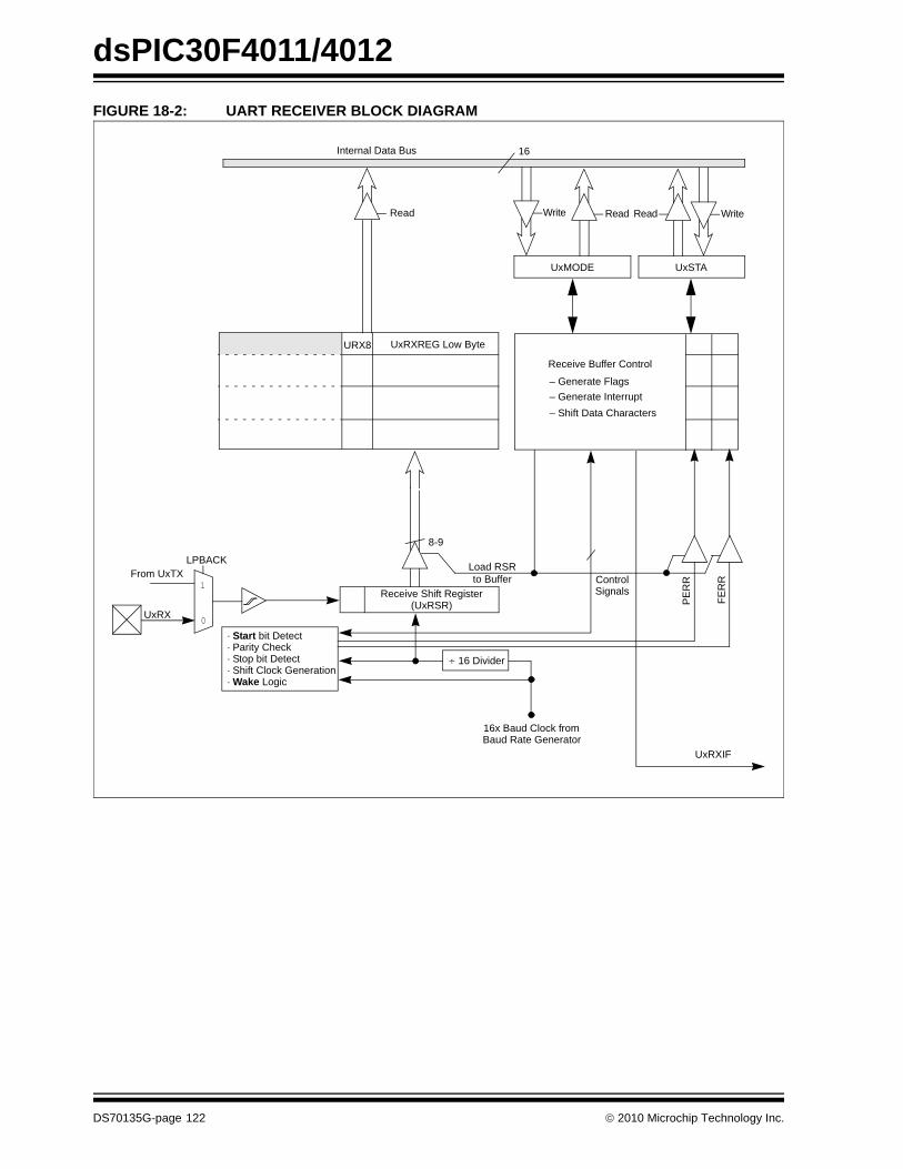
dsPIC30F4011/4012
FIGURE 18-2: UART RECEIVER BLOCK DIAGRAMRead
URX8 UxRXREG Low Byte
Load RSR
UxMODE
Receive Buffer Control
– Generate Flags– Generate Interrupt
UxRXIF
UxRX
· Start bit Detect
Receive Shift RegisterControlSignals
UxSTA
– Shift Data Characters
Read ReadWrite Write
to Buffer
8-9
(UxRSR) PE
RR
FER
R
· Parity Check· Stop bit Detect· Shift Clock Generation· Wake Logic
16Internal Data Bus
1
0
LPBACKFrom UxTX
16x Baud Clock fromBaud Rate Generator
÷ 16 Divider
DS70135G-page 122 © 2010 Microchip Technology Inc.

dsPIC30F4011/4012
18.2 Enabling and Setting Up UART18.2.1 ENABLING THE UARTThe UART module is enabled by setting the UARTENbit in the UxMODE register (where x = 1 or 2). Onceenabled, the UxTX and UxRX pins are configured as anoutput and an input, respectively, overriding the TRISand LATCH register bit settings for the correspondingI/O port pins. The UxTX pin is at logic ‘1’ when notransmission is taking place.
18.2.2 DISABLING THE UARTThe UART module is disabled by clearing the UARTENbit in the UxMODE register. This is the default stateafter any Reset. If the UART is disabled, all I/O pinsoperate as port pins under the control of the LATCH andTRIS bits of the corresponding port pins.
Disabling the UART module resets the buffers toempty states. Any data characters in the buffers arelost and the baud rate counter is reset.
All error and status flags associated with the UARTmodule are reset when the module is disabled. TheURXDA, OERR, FERR, PERR, UTXEN, UTXBRK andUTXBF bits are cleared, whereas RIDLE and TRMTare set. Other control bits, including ADDEN,URXISEL<1:0>, UTXISEL, as well as the UxMODEand UxBRG registers, are not affected.
Clearing the UARTEN bit while the UART is active willabort all pending transmissions and receptions andreset the module as defined above. Re-enabling theUART will restart the UART in the same configuration.
18.2.3 ALTERNATE I/OThe alternate I/O function is enabled by setting theALTIO bit (UxMODE<10>). If ALTIO = 1, the UxATXand UxARX pins (alternate transmit and alternatereceive pins, respectively) are used by the UART mod-ule instead of the UxTX and UxRX pins. If ALTIO = 0,the UxTX and UxRX pins are used by the UARTmodule.
18.2.4 SETTING UP DATA, PARITY AND STOP BIT SELECTIONS
Control bits, PDSEL<1:0> in the UxMODE register, areused to select the data length and parity used in thetransmission. The data length may either be 8 bits witheven, odd or no parity, or 9-bits with no parity.
The STSEL bit determines whether one or two Stop bitswill be used during data transmission.
The default (power-on) setting of the UART is 8 bits, noparity and 1 Stop bit (typically represented as 8, N, 1).
18.3 Transmitting Data
18.3.1 TRANSMITTING IN 8-BIT DATA MODE
The following steps must be performed in order totransmit 8-bit data:
1. Set up the UART:First, the data length, parity and number of Stopbits must be selected. Then, the transmit andreceive interrupt enable and priority bits are setup in the UxMODE and UxSTA registers. Also,the appropriate baud rate value must be writtento the UxBRG register.
2. Enable the UART by setting the UARTEN bit(UxMODE<15>).
3. Set the UTXEN bit (UxSTA<10>), therebyenabling a transmission.
4. Write the byte to be transmitted to the lower byteof UxTXREG. The value will be transferred to theTransmit Shift register (UxTSR) immediatelyand the serial bit stream will start shifting outduring the next rising edge of the baud clock.Alternatively, the data byte may be written whileUTXEN = 0, following which, the user may setUTXEN. This will cause the serial bit stream tobegin immediately because the baud clock willstart from a cleared state.
5. A transmit interrupt will be generated dependingon the value of the interrupt control bit UTXISEL(UxSTA<15>).
18.3.2 TRANSMITTING IN 9-BIT DATA MODE
The sequence of steps involved in the transmission of9-bit data is similar to 8-bit transmission, except that a16-bit data word (of which the upper 7 bits are alwaysclear) must be written to the UxTXREG register.
18.3.3 TRANSMIT BUFFER (UXTXB)The transmit buffer is 9 bits wide and 4 charactersdeep. Including the Transmit Shift register (UxTSR),the user effectively has a 5-deep FIFO (First In FirstOut) buffer. The UTXBF Status bit (UxSTA<9>)indicates whether the transmit buffer is full.
If a user attempts to write to a full buffer, the new datawill not be accepted into the FIFO, and no data shiftwill occur within the buffer. This enables recovery froma buffer overrun condition.
The FIFO is reset during any device Reset, but is notaffected when the device enters or wakes up from apower-saving mode.
© 2010 Microchip Technology Inc. DS70135G-page 123

dsPIC30F4011/4012
18.3.4 TRANSMIT INTERRUPTThe Transmit Interrupt Flag (U1TXIF or U2TXIF) islocated in the corresponding interrupt flag register.The transmitter generates an edge to set the UxTXIFbit. The condition for generating the interrupt dependson UTXISEL control bit:
a) If UTXISEL = 0, an interrupt is generated when aword is transferred from the transmit buffer to theTransmit Shift register (UxTSR). This implies thatthe transmit buffer has at least one empty word.
b) If UTXISEL = 1, an interrupt is generated whena word is transferred from the transmit buffer tothe Transmit Shift register (UxTSR) and thetransmit buffer is empty.
Switching between the two interrupt modes duringoperation is possible and sometimes offers moreflexibility.
18.3.5 TRANSMIT BREAKSetting the UTXBRK bit (UxSTA<11>) will cause theUxTX line to be driven to logic ‘0’. The UTXBRK bitoverrides all transmission activity. Therefore, the usershould generally wait for the transmitter to be Idlebefore setting UTXBRK.
To send a Break character, the UTXBRK bit must beset by software and must remain set for a minimum of13 baud clock cycles. The UTXBRK bit is then clearedby software to generate Stop bits. The user must waitfor a duration of at least one or two baud clock cyclesin order to ensure a valid Stop bit(s) before reloadingthe UxTXB or starting other transmitter activity.Transmission of a Break character does not generatea transmit interrupt.
18.4 Receiving Data
18.4.1 RECEIVING IN 8-BIT OR 9-BIT DATA MODE
The following steps must be performed while receiving8-bit or 9-bit data:
1. Set up the UART (see Section 18.3.1“Transmitting in 8-bit Data Mode”).
2. Enable the UART (see Section 18.3.1“Transmitting in 8-bit Data Mode”).
3. A receive interrupt will be generated when oneor more data words have been received,depending on the receive interrupt settingsspecified by the URXISEL bits (UxSTA<7:6>).
4. Read the OERR bit to determine if an overrunerror has occurred. The OERR bit must be resetin software.
5. Read the received data from UxRXREG. The actof reading UxRXREG will move the next word tothe top of the receive FIFO and the PERR andFERR values will be updated.
18.4.2 RECEIVE BUFFER (UXRXB)The receive buffer is 4 words deep. Including theReceive Shift register (UxRSR), the user effectivelyhas a 5-word deep FIFO buffer.
URXDA (UxSTA<0>) = 1 indicates that the receivebuffer has data available. URXDA = 0 implies that thebuffer is empty. If a user attempts to read an emptybuffer, the old values in the buffer will be read and nodata shift will occur within the FIFO.
The FIFO is reset during any device Reset. It is notaffected when the device enters or wakes up from apower-saving mode.
18.4.3 RECEIVE INTERRUPTThe Receive Interrupt Flag (U1RXIF or U2RXIF) canbe read from the corresponding interrupt flag register.The interrupt flag is set by an edge generated by thereceiver. The condition for setting the receive interruptflag depends on the settings specified by theURXISEL<1:0> (UxSTA<7:6>) control bits.
a) If URXISEL<1:0> = 00 or 01, an interrupt isgenerated every time a data word is transferredfrom the Receive Shift register (UxRSR) to thereceive buffer. There may be one or morecharacters in the receive buffer.
b) If URXISEL<1:0> = 10, an interrupt is generatedwhen a word is transferred from the ReceiveShift register (UxRSR) to the receive bufferwhich, as a result of the transfer, contains3 characters.
c) If URXISEL<1:0> = 11, an interrupt is set whena word is transferred from the Receive Shiftregister (UxRSR) to the receive buffer which, asa result of the transfer, contains 4 characters(i.e., becomes full).
Switching between the interrupt modes duringoperation is possible, though generally not advisableduring normal operation.
18.5 Reception Error Handling
18.5.1 RECEIVE BUFFER OVERRUN ERROR (OERR BIT)
The OERR bit (UxSTA<1>) is set if all of the followingconditions occur:
a) The receive buffer is full.b) The Receive Shift register is full, but unable to
transfer the character to the receive buffer.c) The Stop bit of the character in the UxRSR is
detected, indicating that the UxRSR needs totransfer the character to the buffer.
Once OERR is set, no further data is shifted in UxRSR(until the OERR bit is cleared in software or a Resetoccurs). The data held in UxRSR and UxRXREGremains valid.
DS70135G-page 124 © 2010 Microchip Technology Inc.

dsPIC30F4011/4012
18.5.2 FRAMING ERROR (FERR)The FERR bit (UxSTA<2>) is set if a ‘0’ is detectedinstead of a Stop bit. If two Stop bits are selected, bothStop bits must be ‘1’, otherwise FERR will be set. Theread-only FERR bit is buffered along with the receiveddata; it is cleared on any Reset.18.5.3 PARITY ERROR (PERR)The PERR bit (UxSTA<3>) is set if the parity of thereceived word is incorrect. This error bit is applicableonly if a Parity mode (odd or even) is selected. Theread-only PERR bit is buffered along with the receiveddata bytes; it is cleared on any Reset.
18.5.4 IDLE STATUSWhen the receiver is active (i.e., between the initialdetection of the Start bit and the completion of the Stopbit), the RIDLE bit (UxSTA<4>) is ‘0’. Between thecompletion of the Stop bit and detection of the nextStart bit, the RIDLE bit is ‘1’, indicating that the UARTis Idle.
18.5.5 RECEIVE BREAKThe receiver will count and expect a certain numberof bit times based on the values programmed inthe PDSEL<1:0> (UxMODE<2:1>) and STSEL(UxMODE<0>) bits.
If the Break is longer than 13 bit times, the reception isconsidered complete after the number of bit timesspecified by PDSEL and STSEL. The URXDA bit isset, FERR is set, zeros are loaded into the receiveFIFO, interrupts are generated, if appropriate and theRIDLE bit is set.
When the module receives a long Break signal and thereceiver has detected the Start bit, the data bits andthe invalid Stop bit (which sets the FERR), the receivermust wait for a valid Stop bit before looking for the nextStart bit. It cannot assume that the Break condition onthe line is the next Start bit.
Break is regarded as a character containing all ‘0’s,with the FERR bit set. The Break character is loadedinto the buffer. No further reception can occur until aStop bit is received. Note that RIDLE goes high whenthe Stop bit has not been received yet.
18.6 Address Detect ModeSetting the ADDEN bit (UxSTA<5>) enables thisspecial mode in which a 9th bit (URX8) value of ‘1’identifies the received word as an address, rather thandata. This mode is only applicable for 9-bit datacommunication. The URXISELx control bit does nothave any impact on interrupt generation in this mode,since an interrupt (if enabled) will be generated everytime the received word has the 9th bit set.
18.7 Loopback ModeSetting the LPBACK bit enables this special mode inwhich the UxTX pin is internally connected to the UxRXpin. When configured for the Loopback mode, theUxRX pin is disconnected from the internal UARTreceive logic. However, the UxTX pin still functions asin a normal operation.
To select this mode:
a) Configure UART for desired mode of operation.b) Set LPBACK = 1 to enable Loopback mode.c) Enable transmission as defined in Section 18.3
“Transmitting Data”.
18.8 Baud Rate GeneratorThe UART has a 16-bit Baud Rate Generator to allowmaximum flexibility in baud rate generation. The BaudRate Generator register (UxBRG) is readable andwritable. The baud rate is computed as follows:
BRG = 16-bit value held in UxBRG register (0 through 65535)
FCY = Instruction Clock Rate (1/TCY)
The baud rate is given by Equation 18-1.
EQUATION 18-1: BAUD RATE
Therefore, maximum baud rate possible is:
FCY/16 (if BRG = 0),
and the minimum baud rate possible is:
FCY/(16 * 65536).
With a full, 16-bit Baud Rate Generator, at 30 MIPSoperation, the minimum baud rate achievable is28.5 bps.
Baud Rate = FCY/(16 * (BRG + 1))
© 2010 Microchip Technology Inc. DS70135G-page 125

dsPIC30F4011/4012
18.9 Auto-Baud SupportTo allow the system to determine baud rates ofreceived characters, the input can be optionally linkedto a selected capture input (IC1 for UART1, IC2 forUART2). To enable this mode, the user must programthe input capture module to detect the falling and risingedges of the Start bit.18.10 UART Operation During CPU Sleep and Idle Modes
18.10.1 UART OPERATION DURING CPU SLEEP MODE
When the device enters Sleep mode, all clock sourcesto the module are shut down and stay at logic ‘0’. Ifentry into Sleep mode occurs while a transmission isin progress, then the transmission is aborted. TheUxTX pin is driven to logic ‘1’. Similarly, if entry intoSleep mode occurs while a reception is in progress,then the reception is aborted. The UxSTA, UxMODE,UxBRG, transmit and receive registers and buffers, arenot affected by Sleep mode.
If the WAKE bit (UxMODE<7>) is set before the deviceenters Sleep mode, then a falling edge on the UxRXpin will generate a receive interrupt. The ReceiveInterrupt Select Mode bit (URXISEL) has no effect forthis function. If the receive interrupt is enabled, thenthis will wake-up the device from Sleep. The UARTENbit must be set in order to generate a wake-upinterrupt.
18.10.2 UART OPERATION DURING CPU IDLE MODE
For the UART, the USIDL bit selects if the module willstop operation when the device enters Idle mode, orwhether the module will continue on Idle. If USIDL = 0,the module will continue operation during Idle mode. IfUSIDL = 1, the module will stop on Idle.
DS70135G-page 126 © 2010 Microchip Technology Inc.

© 2010 M
icrochip Technology Inc.D
S70135G
-page 127
dsPIC30F4011/4012
TA
TA
SF 2 Bit 1 Bit 0 Reset State
U1 EL1 PDSEL0 STSEL 0000 0000 0000 0000
U1 R OERR URXDA 0000 0001 0001 0000
U1 0000 000u uuuu uuuu
U1 0000 0000 0000 0000
U1 0000 0000 0000 0000
LeNo
2 Bit 1 Bit 0 Reset State
U2 L1 PDSEL0 STSEL 0000 0000 0000 0000
U2 R OERR URXDA 0000 0001 0001 0000
U2 0000 000u uuuu uuuu
U2 0000 0000 0000 0000
U2 0000 0000 0000 0000
LeNo
BLE 18-1: UART1 REGISTER MAP(1)
BLE 18-2: UART2 REGISTER MAP (NOT AVAILABLE ON dsPIC30F4012)(1)
R Name Addr. Bit 15 Bit 14 Bit 13 Bit 12 Bit 11 Bit 10 Bit 9 Bit 8 Bit 7 Bit 6 Bit 5 Bit 4 Bit 3 Bit
MODE 020C UARTEN — USIDL — — ALTIO — — WAKE LPBACK ABAUD — — PDS
STA 020E UTXISEL — — — UTXBRK UTXEN UTXBF TRMT URXISEL1 URXISEL0 ADDEN RIDLE PERR FER
TXREG 0210 — — — — — — — UTX8 Transmit Register
RXREG 0212 — — — — — — — URX8 Receive Register
BRG 0214 Baud Rate Generator Prescaler
gend: u = uninitialized bit; — = unimplemented bit, read as ‘0’te 1: Refer to the “dsPIC30F Family Reference Manual” (DS70046) for descriptions of register bit fields.
SFR Name Addr. Bit 15 Bit 14 Bit 13 Bit 12 Bit 11 Bit 10 Bit 9 Bit 8 Bit 7 Bit 6 Bit 5 Bit 4 Bit 3 Bit
MODE 0216 UARTEN — USIDL — — — — — WAKE LPBACK ABAUD — — PDSE
STA 0218 UTXISEL — — — UTXBRK UTXEN UTXBF TRMT URXISEL1 URXISEL0 ADDEN RIDLE PERR FER
TXREG 021A — — — — — — — UTX8 Transmit Register
RXREG 021C — — — — — — — URX8 Receive Register
BRG 021E Baud Rate Generator Prescaler
gend: u = uninitialized bit; — = unimplemented bit, read as ‘0’te 1: Refer to the “dsPIC30F Family Reference Manual” (DS70046) for descriptions of register bit fields.

dsPIC30F4011/4012
NOTES:DS70135G-page 128 © 2010 Microchip Technology Inc.

dsPIC30F4011/4012
19.0 CAN MODULE
19.1 Overview The Controller Area Network (CAN) module is a serialinterface, useful for communicating with other CANmodules or digital signal controller devices. This inter-face/protocol was designed to allow communicationswithin noisy environments. The dsPIC30F4011/4012devices have 1 CAN module.
The CAN module is a communication controller imple-menting the CAN 2.0 A/B protocol, as defined in theBOSCH specification. The module will support CAN 1.2,CAN 2.0A, CAN2.0B Passive and CAN 2.0B Activeversions of the protocol. The module implementation isa full CAN system. The CAN specification is not coveredwithin this data sheet. The reader may refer to theBOSCH CAN specification for further details.
The module features are as follows:
• Implementation of the CAN protocol CAN 1.2, CAN 2.0A and CAN 2.0B
• Standard and extended data frames• 0-8 bytes data length• Programmable bit rate up to 1 Mbit/sec• Support for remote frames• Double-buffered receiver with two prioritized
received message storage buffers (each buffer may contain up to 8 bytes of data)
• 6 full (standard/extended identifier), acceptance filters, 2 associated with the high priority receive buffer and 4 associated with the low priority receive buffer
• 2 full, acceptance filter masks, one each associated with the high and low priority receive buffers
• Three transmit buffers with application specified prioritization and abort capability (each buffer may contain up to 8 bytes of data)
• Programmable wake-up functionality with integrated low-pass filter
• Programmable Loopback mode supports self-test operation
• Signaling via interrupt capabilities for all CAN receiver and transmitter error states
• Programmable clock source
• Programmable link to input capture module (IC2, for both CAN1 and CAN2) for time-stamping and network synchronization
• Low-power Sleep and Idle mode
The CAN bus module consists of a protocol engine andmessage buffering/control. The CAN protocol enginehandles all functions for receiving and transmittingmessages on the CAN bus. Messages are transmittedby first loading the appropriate data registers. Statusand errors can be checked by reading the appropriateregisters. Any message detected on the CAN bus ischecked for errors and then matched against filters tosee if it should be received and stored in one of thereceive registers.
19.2 Frame TypesThe CAN module transmits various types of frameswhich include data messages or remote transmissionrequests, initiated by the user, as other frames that areautomatically generated for control purposes. Thefollowing frame types are supported:
19.2.1 STANDARD DATA FRAMEA standard data frame is generated by a node when thenode wishes to transmit data. It includes an 11-bitStandard Identifier (SID) but not an 18-bit ExtendedIdentifier (EID).
19.2.2 EXTENDED DATA FRAMEAn extended data frame is similar to a standard dataframe but includes an extended identifier as well.
19.2.3 REMOTE FRAMEIt is possible for a destination node to request the datafrom the source. For this purpose, the destination nodesends a remote frame with an identifier that matchesthe identifier of the required data frame. Theappropriate data source node will then send a dataframe as a response to this remote request.
19.2.4 ERROR FRAMEAn error frame is generated by any node that detects abus error. An error frame consists of 2 fields: an errorflag field and an error delimiter field.
19.2.5 OVERLOAD FRAME An overload frame can be generated by a node as aresult of 2 conditions. First, the node detects a domi-nant bit during interframe space which is an illegalcondition. Second, due to internal conditions, the nodeis not yet able to start reception of the next message. Anode may generate a maximum of 2 sequentialoverload frames to delay the start of the next message.
19.2.6 INTERFRAME SPACEInterframe space separates a proceeding frame (ofwhatever type) from a following data or remote frame.
Note: This data sheet summarizes features ofthis group of dsPIC30F devices and is notintended to be a complete referencesource. For more information on the CPU,peripherals, register descriptions andgeneral device functionality, refer to thedsPIC30F Family Reference Manual(DS70046). For more information on thedevice instruction set and programming,refer to the “16-bit MCU and DSCReference Manual” (DS70157).
© 2010 Microchip Technology Inc. DS70135G-page 129

dsPIC30F4011/4012
FIGURE 19-1: CAN BUFFERS AND PROTOCOL ENGINE BLOCK DIAGRAMAcceptance FilterRXF2(1)
Accept
Accept
Identifier
Data Field Data Field
Identifier
Acceptance MaskRXM1(1)
Acceptance FilterRXF3(1)
Acceptance FilterRXF4(1)
Acceptance FilterRXF5(1)
MAB
Acceptance MaskRXM0(1)
Acceptance FilterRXF0(1)
Acceptance FilterRXF1(1)
RXB0(1)
TXR
EQ
TXB2(1)
TXA
BT
TXLA
RB
TXE
RR
MES
SAG
E
MessageQueueControl
Transmit Byte Sequencer
TXR
EQ
TXB1(1)
TXA
BT
TXLA
RB
TXE
RR
MES
SAG
E
TXR
EQ
TXB0(1)
TXA
BT
TXLA
RB
TXE
RR
MES
SAG
E
Receive ShiftTransmit Shift
ReceiveError
TransmitError
Protocol
RERRCNT
TERRCNT
ErrPasBusOff
FiniteState
Machine
Counter
Counter
TransmitLogic
BitTimingLogic
C1TX C1RX
Bit TimingGenerator
PROTOCOLENGINE
BUFFERS
CRC CheckCRC Generator
RXB1(1)
Note 1: These are conceptual groups of registers, not SFR names by themselves.
DS70135G-page 130 © 2010 Microchip Technology Inc.

dsPIC30F4011/4012
19.3 Modes of OperationThe CAN module can operate in one of severaloperation modes selected by the user. These modesinclude:• Initialization Mode• Disable Mode• Normal Operation Mode• Listen Only Mode• Loopback Mode• Error Recognition Mode
Modes are requested by setting the REQOP<2:0> bits(C1CTRL<10:8>). Entry into a mode is acknowledged bymonitoring the OPMODE<2:0> bits (C1CTRL<7:5>). Themodule will not change the mode and the OPMODE bitsuntil a change in mode is acceptable, generally duringbus Idle time which is defined as at least 11 consecutiverecessive bits.
19.3.1 INITIALIZATION MODEIn the Initialization mode, the module will not transmit orreceive. The error counters are cleared and the inter-rupt flags remain unchanged. The programmer willhave access to Configuration registers that are accessrestricted in other modes. The module will protect theuser from accidentally violating the CAN protocolthrough programming errors. All registers which controlthe configuration of the module can not be modifiedwhile the module is online. The CAN module will not beallowed to enter the Configuration mode while atransmission is taking place. The Configuration modeserves as a lock to protect the following registers.
• All Module Control Registers• Baud Rate and Interrupt Configuration Registers • Bus Timing Registers • Identifier Acceptance Filter Registers • Identifier Acceptance Mask Registers
19.3.2 DISABLE MODEIn Disable mode, the module will not transmit orreceive. The module has the ability to set the WAKIF bitdue to bus activity, however, any pending interrupts willremain and the error counters will retain their value.
If the REQOP<2:0> bits (C1CTRL<10:8>) = 001, themodule will enter the Disable mode. If the module isactive, the module will wait for 11 recessive bits on theCAN bus, detect that condition as an Idle bus, thenaccept the disable command. When theOPMODE<2:0> bits (C1CTRL<7:5>) = 001, thatindicates whether the module successfully went intoDisable mode. The I/O pins will revert to normal I/Ofunction when the module is in the Disable mode.
The module can be programmed to apply a low-passfilter function to the C1RX input line while the moduleor the CPU is in Sleep mode. The WAKFIL bit(C1CFG2<14>) enables or disables the filter.
19.3.3 NORMAL OPERATION MODENormal Operation mode is selected whenREQOP<2:0> = 000. In this mode, the module isactivated and the I/O pins will assume the CAN busfunctions. The module will transmit and receive CANbus messages via the C1TX and C1RX pins.
19.3.4 LISTEN ONLY MODEIf the Listen Only mode is activated, the module on theCAN bus is passive. The transmitter buffers revert tothe port I/O function. The receive pins remain inputs.For the receiver, no error flags or Acknowledge signalsare sent. The error counters are deactivated in thisstate. The Listen Only mode can be used for detectingthe baud rate on the CAN bus. To use this, it isnecessary that there are at least two further nodes thatcommunicate with each other.
19.3.5 ERROR RECOGNITION MODEThe module can be set to ignore all errors and receiveany message. In this mode, the data which is in themessage assembly buffer until the time an erroroccurred, is copied in the receive buffer and can beread via the CPU interface.
19.3.6 LOOPBACK MODEIf the Loopback mode is activated, the module willconnect the internal transmit signal to the internalreceive signal at the module boundary. The transmitand receive pins revert to their port I/O function.
Note: Typically, if the CAN module is allowed totransmit in a particular mode of operationand a transmission is requested immedi-ately after the CAN module has beenplaced in that mode of operation, themodule waits for 11 consecutive recessivebits on the bus before starting transmission.If the user switches to Disable mode withinthis 11-bit period, then this transmission isaborted and the corresponding TXABT bitis set and TXREQ bit is cleared.
© 2010 Microchip Technology Inc. DS70135G-page 131

dsPIC30F4011/4012
19.4 Message Reception19.4.1 RECEIVE BUFFERSThe CAN bus module has 3 receive buffers. However,one of the receive buffers is always committed to mon-itoring the bus for incoming messages. This buffer iscalled the message assembly buffer (MAB). There aretwo receive buffers, visibly denoted as RXB0 andRXB1, that can essentially instantaneously receive acomplete message from the protocol engine.
All messages are assembled by the MAB, and aretransferred to the RXBn buffers only if the acceptancefilter criterion is met. When a message is received, theRXxIF flag (C1INTF<0> or C1INIF<1>) will be set. Thisbit can only be set by the module when a message isreceived. The bit is cleared by the CPU when it hascompleted processing the message in the buffer. If theRXxIE bit (C1INTE<0> or C1INTE<1>) is set, aninterrupt will be generated when a message isreceived.
RXF0 and RXF1 filters with the RXM0 mask areassociated with RXB0. The filters, RXF2, RXF3, RXF4and RXF5, and the mask, RXM1, are associated withRXB1.
19.4.2 MESSAGE ACCEPTANCE FILTERSThe message acceptance filters and masks are used todetermine if a message in the message assembly buf-fer should be loaded into either of the receive buffers.Once a valid message has been received into the Mes-sage Assembly Buffer (MAB), the identifier fields of themessage are compared to the filter values. If there is amatch, that message will be loaded into the appropriatereceive buffer.
The acceptance filter looks at incoming messages forthe RXIDE bit (CiRXnSID<0>) to determine how tocompare the identifiers. If the RXIDE bit is clear, themessage is a standard frame and only filters with theEXIDE bit (C1RXFxSID<0>) clear are compared. If theRXIDE bit is set, the message is an extended frameand only filters with the EXIDE bit set are compared.
19.4.3 MESSAGE ACCEPTANCE FILTER MASKS
The mask bits essentially determine which bits to applythe filter to. If any mask bit is set to a zero, then that bitwill automatically be accepted regardless of the filterbit. There are 2 programmable acceptance filter masksassociated with the receive buffers, one for each buffer.
19.4.4 RECEIVE OVERRUNAn overrun condition occurs when the MessageAssembly Buffer (MAB) has assembled a validreceived message, the message is accepted throughthe acceptance filters, and when the receive bufferassociated with the filter has not been designated asclear of the previous message.
The overrun error flag, RXxOVR (C1INTF<15> orC1INTF<14>) and the ERRIF bit (C1INTF<5>) will beset and the message in the MAB will be discarded.
If the DBEN bit is clear, RXB1 and RXB0 operate inde-pendently. When this is the case, a message intendedfor RXB0 will not be diverted into RXB1 if RXB0contains an unread message and the RX0OVR bit willbe set.
If the DBEN bit is set, the overrun for RXB0 is handleddifferently. If a valid message is received for RXB0 andRXFUL = 1, it indicates that RXB0 is full andRXFUL = 0 indicates that RXB1 is empty, the messagefor RXB0 will be loaded into RXB1. An overrun error willnot be generated for RXB0. If a valid message isreceived for RXB0 and RXFUL = 1, and RXFUL = 1indicates that both RXB0 and RXB1 are full, themessage will be lost and an overrun will be indicatedfor RXB1.
19.4.5 RECEIVE ERRORSThe CAN module will detect the following receiveerrors:
• Cyclic Redundancy Check (CRC) Error• Bit Stuffing Error• Invalid Message Receive Error
The receive error counter is incremented by one incase one of these errors occur. The RXWAR bit(C1INTF<9>) indicates that the receive error counterhas reached the CPU warning limit of 96 and aninterrupt is generated.
19.4.6 RECEIVE INTERRUPTSReceive interrupts can be divided into 3 major groups,each including various conditions that generateinterrupts:
19.4.6.1 Receive InterruptA message has been successfully received and loadedinto one of the receive buffers. This interrupt is acti-vated immediately after receiving the End-of-Frame(EOF) field. Reading the RXxIF flag will indicate whichreceive buffer caused the interrupt.
19.4.6.2 Wake-up InterruptThe CAN module has woken up from Disable mode orthe device has woken up from Sleep mode.
DS70135G-page 132 © 2010 Microchip Technology Inc.

dsPIC30F4011/4012
19.4.6.3 Receive Error InterruptsA receive error interrupt will be indicated by the ERRIFbit. This bit shows that an error condition occurred. Thesource of the error can be determined by checking thebits in the CAN Interrupt Status register, C1INTF.• Invalid message received.• If any type of error occurred during reception of
the last message, an error will be indicated by the IVRIF bit.
• Receiver overrun.• The RXxOVR bit indicates that an overrun
condition occurred.• Receiver warning.• The RXWAR bit indicates that the Receive Error
Counter (RERRCNT<7:0>) has reached the warning limit of 96.
• Receiver error passive.• The RXEP bit indicates that the Receive Error
Counter has exceeded the error passive limit of 127 and the module has gone into error passive state.
19.5 Message Transmission
19.5.1 TRANSMIT BUFFERSThe CAN module has three transmit buffers. Each ofthe three buffers occupies 14 bytes of data. Eight of thebytes are the maximum 8 bytes of the transmitted mes-sage. Five bytes hold the standard and extendedidentifiers and other message arbitration information.
19.5.2 TRANSMIT MESSAGE PRIORITYTransmit priority is a prioritization within each node of thepending transmittable messages. There are 4 levels oftransmit priority. If TXPRI<1:0> (C1TXxCON<1:0>, wherex = 0, 1 or 2, represents a particular transmit buffer) for aparticular message buffer is set to ‘11’, that buffer has thehighest priority. If TXPRI<1:0> for a particular messagebuffer is set to ‘10’ or ‘01’, that buffer has an intermediatepriority. If TXPRI<1:0> for a particular message buffer is‘00’, that buffer has the lowest priority.
19.5.3 TRANSMISSION SEQUENCETo initiate transmission of the message, the TXREQ bit(C1TXxCON<3>) must be set. The CAN bus moduleresolves any timing conflicts between setting of theTXREQ bit and the Start-of-Frame (SOF), ensuringthat if the priority was changed, it is resolved correctlybefore the SOF occurs. When TXREQ is set, theTXABT (C1TXxCON<6>), TXLARB (C1TXxCON<5>)and TXERR (C1TXxCON<4>) flag bits areautomatically cleared.
Setting TXREQ bit simply flags a message buffer asenqueued for transmission. When the module detectsan available bus, it begins transmitting the messagewhich has been determined to have the highest priority.
If the transmission completes successfully on the firstattempt, the TXREQ bit is cleared automatically and aninterrupt is generated if TXxIE was set.
If the message transmission fails, one of the errorcondition flags will be set and the TXREQ bit willremain set, indicating that the message is still pendingfor transmission. If the message encountered an errorcondition during the transmission attempt, the TXERRbit will be set and the error condition may cause aninterrupt. If the message loses arbitration during thetransmission attempt, the TXLARB bit is set. Nointerrupt is generated to signal the loss of arbitration.
19.5.4 ABORTING MESSAGE TRANSMISSION
The system can also abort a message by clearing theTXREQ bit associated with each message buffer. Set-ting the ABAT bit (C1CTRL<12>) will request an abortof all pending messages. If the message has not yetstarted transmission, or if the message started but isinterrupted by loss of arbitration or an error, the abortwill be processed. The abort is indicated when themodule sets the TXABT bit, and the TXxIF flag is notautomatically set.
19.5.5 TRANSMISSION ERRORSThe CAN module will detect the following transmissionerrors:
• Acknowledge Error• Form Error• Bit Error
These transmission errors will not necessarily generatean interrupt but are indicated by the transmission errorcounter. However, each of these errors will cause thetransmission error counter to be incremented by one.Once the value of the error counter exceeds the valueof 96, the ERRIF (C1INTF<5>) and the TXWAR bit(C1INTF<10>) are set. Once the value of the errorcounter exceeds the value of 96, an interrupt isgenerated and the TXWAR bit in the error flag registeris set.
© 2010 Microchip Technology Inc. DS70135G-page 133

dsPIC30F4011/4012
19.5.6 TRANSMIT INTERRUPTSTransmit interrupts can be divided into 2 major groups,each including various conditions that generateinterrupts:• Transmit Interrupt
At least one of the three transmit buffers is empty (notscheduled) and can be loaded to schedule a messagefor transmission. Reading the TXxIF flags will indicatewhich transmit buffer is available and caused theinterrupt.
• Transmit Error Interrupts
A transmission error interrupt will be indicated by theERRIF flag. This flag shows that an error conditionoccurred. The source of the error can be determined bychecking the error flags in the CAN Interrupt Status reg-ister, C1INTF. The flags in this register are related toreceive and transmit errors.
• Transmitter warning interrupt.• The TXWAR bit indicates that the Transmit Error
Counter has reached the CPU warning limit of 96. • Transmitter error passive.• The TXEP bit (C1INTF<12>) indicates that the
Transmit Error Counter has exceeded the error passive limit of 127 and the module has gone to error passive state.
• Bus off. • The TXBO bit (C1INTF<13>) indicates that the
Transmit Error Counter (TERRCNT<7:0>) has exceeded 255 and the module has gone to bus off state.
19.6 Baud Rate SettingAll nodes on any particular CAN bus must have thesame nominal bit rate. In order to set the baud rate, thefollowing parameters have to be initialized:
• Synchronization Jump Width• Baud Rate Prescaler • Phase Segments• Length Determination of Phase2 Seg • Sample Point • Propagation Segment Bits
19.6.1 BIT TIMING
All controllers on the CAN bus must have the samebaud rate and bit length. However, different controllersare not required to have the same master oscillatorclock. At different clock frequencies of the individualcontrollers, the baud rate has to be adjusted byadjusting the number of time quanta in each segment.
The nominal bit time can be thought of as being dividedinto separate non-overlapping time segments. Thesesegments are shown in Figure 19-2.
• Synchronization segment (Sync Seg)• Propagation time segment (Prop Seg)• Phase segment 1 (Phase1 Seg)• Phase segment 2 (Phase2 Seg)
The time segments and also the nominal bit time aremade up of integer units of time called time quanta orTQ. By definition, the nominal bit time has a minimumof 8 TQ and a maximum of 25 TQ. Also, by definition,the minimum nominal bit time is 1 μsec, correspondingto a maximum bit rate of 1 MHz.
FIGURE 19-2: CAN BIT TIMING
Input Signal
SyncProp
SegmentPhase
Segment 1Phase
Segment 2 Sync
Sample Point
TQ
DS70135G-page 134 © 2010 Microchip Technology Inc.

dsPIC30F4011/4012
19.6.2 PRESCALER SETTINGThere is a programmable prescaler with integral valuesranging from 1 to 64 in addition to a fixed divide-by-2 forclock generation. The Time Quantum (TQ) is a fixedunit of time derived from the oscillator period, shown inEquation 19-1, where FCAN is FCY (if the CANCKS bitis set) or 4 FCY (if CANCKS is cleared).EQUATION 19-1: TIME QUANTUM FOR CLOCK GENERATION
19.6.3 PROPAGATION SEGMENT This part of the bit time is used to compensate physicaldelay times within the network. These delay times con-sist of the signal propagation time on the bus line andthe internal delay time of the nodes. The propagationsegment can be programmed from 1 TQ to 8 TQ bysetting the PRSEG<2:0> bits (C1CFG2<2:0>).
19.6.4 PHASE SEGMENTSThe phase segments are used to optimally locate thesampling of the received bit within the transmitted bittime. The sampling point is between Phase1 Seg andPhase2 Seg. These segments are lengthened or short-ened by resynchronization. The end of the Phase1 Segdetermines the sampling point within a bit period. Thesegment is programmable from 1 TQ to 8 TQ. Phase2Seg provides delay to the next transmitted data transi-tion. The segment is programmable from 1 TQ to 8 TQ,or it may be defined to be equal to the greater ofPhase1 Seg or the information processing time (2 TQ).The Phase1 Seg is initialized by setting bitsSEG1PH<2:0> (C1CFG2<5:3>), and Phase2 Seg isinitialized by setting SEG2PH<2:0> (C1CFG2<10:8>).
The following requirement must be fulfilled while settingthe lengths of the phase segments:
Propagation Segment + Phase1 Seg > = Phase2 Seg
19.6.5 SAMPLE POINTThe sample point is the point of time at which the buslevel is read and interpreted as the value of that respec-tive bit. The location is at the end of Phase1 Seg. If the bittiming is slow and contains many TQ, it is possible tospecify multiple sampling of the bus line at the samplepoint. The level determined by the CAN bus then cor-responds to the result from the majority decision of threevalues. The majority samples are taken at the samplepoint and twice before with a distance of TQ/2. The CANmodule allows the user to choose between samplingthree times at the same point, or once at the same point,by setting or clearing the SAM bit (C1CFG2<6>).
Typically, the sampling of the bit should take place atabout 60-70% through the bit time depending on thesystem parameters.
19.6.6 SYNCHRONIZATIONTo compensate for phase shifts between the oscillatorfrequencies of the different bus stations, each CANcontroller must be able to synchronize to the relevantsignal edge of the incoming signal. When an edge inthe transmitted data is detected, the logic will comparethe location of the edge to the expected time(synchronous segment). The circuit will then adjust thevalues of Phase1 Seg and Phase2 Seg. There are2 mechanisms used to synchronize.
19.6.6.1 Hard SynchronizationHard synchronization is only done whenever there is a‘recessive’ to ‘dominant’ edge during bus Idle, indicatingthe start of a message. After hard synchronization, thebit time counters are restarted with the synchronoussegment. Hard synchronization forces the edge whichhas caused the hard synchronization to lie within thesynchronization segment of the restarted bit time. If ahard synchronization is done, there will not be aresynchronization within that bit time.
19.6.6.2 ResynchronizationAs a result of resynchronization, Phase1 Seg may belengthened or Phase2 Seg may be shortened. Theamount of lengthening or shortening of the phase buffersegment has an upper bound known as thesynchronization jump width, and is specified by theSJW<1:0> bits (C1CFG1<7:6>). The value of thesynchronization jump width will be added to Phase1 Segor subtracted from Phase2 Seg. The resynchronizationjump width is programmable between 1 TQ and 4 TQ.
The following requirement must be fulfilled while settingthe SJW<1:0> bits:
Phase2 Seg > Synchronization Jump Width
Note: FCAN must not exceed 30 MHz. IfCANCKS = 0, FCY must not exceed 7.5MHz.
TQ = 2 (BRP<5:0> + 1)/FCAN
© 2010 Microchip Technology Inc. DS70135G-page 135

dsPIC30F4011/4012
DS
70135G-page 136
© 2010 M
icrochip Technology Inc.
3 Bit 2 Bit 1 Bit 0 Reset State
— EXIDE 000u uuuu uuuu uu0u
0000 uuuu uuuu uuuu
— — — uuuu uu00 0000 0000
— EXIDE 000u uuuu uuuu uu0u
0000 uuuu uuuu uuuu
— — — uuuu uu00 0000 0000
— EXIDE 000u uuuu uuuu uu0u
0000 uuuu uuuu uuuu
— — — uuuu uu00 0000 0000
— EXIDE 000u uuuu uuuu uu0u
0000 uuuu uuuu uuuu
— — — uuuu uu00 0000 0000
— EXIDE 000u uuuu uuuu uu0u
0000 uuuu uuuu uuuu
— — — uuuu uu00 0000 0000
— EXIDE 000u uuuu uuuu uu0u
0000 uuuu uuuu uuuu
— — — uuuu uu00 0000 0000
— MIDE 000u uuuu uuuu uu0u
0000 uuuu uuuu uuuu
— — — uuuu uu00 0000 0000
— MIDE 000u uuuu uuuu uu0u
0000 uuuu uuuu uuuu
— — — uuuu uu00 0000 0000
:0> SRR TXIDE uuuu u000 uuuu uuuu
ntifier<13:6> uuuu 0000 uuuu uuuu
— — — uuuu uuuu uuuu u000
e 0 uuuu uuuu uuuu uuuu
e 2 uuuu uuuu uuuu uuuu
e 4 uuuu uuuu uuuu uuuu
e 6 uuuu uuuu uuuu uuuu
Q — TXPRI<1:0> 0000 0000 0000 0000
:0> SRR TXIDE uuuu u000 uuuu uuuu
ntifier<13:6> uuuu 0000 uuuu uuuu
— — — uuuu uuuu uuuu u000
e 0 uuuu uuuu uuuu uuuu
TABLE 19-1: CAN1 REGISTER MAP(1)
SFR Name Addr. Bit 15 Bit 14 Bit 13 Bit 12 Bit 11 Bit 10 Bit 9 Bit 8 Bit 7 Bit 6 Bit 5 Bit 4 Bit
C1RXF0SID 0300 — — — Receive Acceptance Filter 0 Standard Identifier<10:0>C1RXF0EIDH 0302 — — — — Receive Acceptance Filter 0 Extended Identifier<17:6>C1RXF0EIDL 0304 Receive Acceptance Filter 0 Extended Identifier<5:0> — — — — — — —C1RXF1SID 0308 — — — Receive Acceptance Filter 1 Standard Identifier<10:0>C1RXF1EIDH 030A — — — — Receive Acceptance Filter 1 Extended Identifier<17:6>C1RXF1EIDL 030C Receive Acceptance Filter 1 Extended Identifier<5:0> — — — — — — —C1RXF2SID 0310 — — — Receive Acceptance Filter 2 Standard Identifier<10:0>C1RXF2EIDH 0312 — — — — Receive Acceptance Filter 2 Extended Identifier<17:6>C1RXF2EIDL 0314 Receive Acceptance Filter 2 Extended Identifier<5:0> — — — — — — —C1RXF3SID 0318 — — — Receive Acceptance Filter 3 Standard Identifier<10:0>C1RXF3EIDH 031A — — — — Receive Acceptance Filter 3 Extended Identifier<17:6>C1RXF3EIDL 031C Receive Acceptance Filter 3 Extended Identifier<5:0> — — — — — — —C1RXF4SID 0320 — — — Receive Acceptance Filter 4 Standard Identifier<10:0>C1RXF4EIDH 0322 — — — — Receive Acceptance Filter 4 Extended Identifier<17:6>C1RXF4EIDL 0324 Receive Acceptance Filter 4 Extended Identifier<5:0> — — — — — — —C1RXF5SID 0328 — — — Receive Acceptance Filter 5 Standard Identifier<10:0>C1RXF5EIDH 032A — — — — Receive Acceptance Filter 5 Extended Identifier<17:6>C1RXF5EIDL 032C Receive Acceptance Filter 5 Extended Identifier<5:0> — — — — — — —C1RXM0SID 0330 — — — Receive Acceptance Mask 0 Standard Identifier<10:0>C1RXM0EIDH 0332 — — — — Receive Acceptance Mask 0 Extended Identifier<17:6>C1RXM0EIDL 0334 Receive Acceptance Mask 0 Extended Identifier<5:0> — — — — — — —C1RXM1SID 0338 — — — Receive Acceptance Mask 1 Standard Identifier<10:0>C1RXM1EIDH 033A — — — — Receive Acceptance Mask 1 Extended Identifier<17:6>C1RXM1EIDL 033C Receive Acceptance Mask 1 Extended Identifier<5:0> — — — — — — —C1TX2SID 0340 Transmit Buffer 2 Standard Identifier<10:6> — — — Transmit Buffer 2 Standard Identifier<5C1TX2EID 0342 Transmit Buffer 2 Extended Identifier<17:14> — — — — Transmit Buffer 2 Extended IdeC1TX2DLC 0344 Transmit Buffer 2 Extended Identifier<5:0> TXRTR TXRB1 TXRB0 DLC<3:0>C1TX2B1 0346 Transmit Buffer 2 Byte 1 Transmit Buffer 2 BytC1TX2B2 0348 Transmit Buffer 2 Byte 3 Transmit Buffer 2 BytC1TX2B3 034A Transmit Buffer 2 Byte 5 Transmit Buffer 2 BytC1TX2B4 034C Transmit Buffer 2 Byte 7 Transmit Buffer 2 BytC1TX2CON 034E — — — — — — — — — TXABT TXLARB TXERR TXREC1TX1SID 0350 Transmit Buffer 1 Standard Identifier<10:6> — — — Transmit Buffer 1 Standard Identifier<5C1TX1EID 0352 Transmit Buffer 1 Extended Identifier<17:14> — — — — Transmit Buffer 1 Extended IdeC1TX1DLC 0354 Transmit Buffer 1 Extended Identifier<5:0> TXRTR TXRB1 TXRB0 DLC<3:0>
C1TX1B1 0356 Transmit Buffer 1 Byte 1 Transmit Buffer 1 BytLegend: u = uninitialized bit; — = unimplemented bit, read as ‘0’Note 1: Refer to the “dsPIC30F Family Reference Manual” (DS70046) for descriptions of register bit fields.

© 2010 M
icrochip Technology Inc.D
S70135G
-page 137
dsPIC30F4011/4012
C1 uuuu uuuu uuuu uuuu
C1 uuuu uuuu uuuu uuuu
C1 uuuu uuuu uuuu uuuu
C1 — TXPRI<1:0> 0000 0000 0000 0000
C1 SRR TXIDE uuuu u000 uuuu uuuu
C1 <13:6> uuuu 0000 uuuu uuuu
C1 — — — uuuu uuuu uuuu u000
C1 uuuu uuuu uuuu uuuu
C1 uuuu uuuu uuuu uuuu
C1 uuuu uuuu uuuu uuuu
C1 uuuu uuuu uuuu uuuu
C1 — TXPRI<1:0> 0000 0000 0000 0000
C1 SRR RXIDE 000u uuuu uuuu uuuu
C1 0000 uuuu uuuu uuuu
C1 DLC<3:0> uuuu uuuu 000u uuuu
C1 uuuu uuuu uuuu uuuu
C1 uuuu uuuu uuuu uuuu
C1 uuuu uuuu uuuu uuuu
C1 uuuu uuuu uuuu uuuu
C1 FILHIT<2:0> 0000 0000 0000 0000
C1 SRR RXIDE 000u uuuu uuuu uuuu
C1 0000 uuuu uuuu uuuu
C1 DLC<3:0> uuuu uuuu 000u uuuu
C1 uuuu uuuu uuuu uuuu
C1 uuuu uuuu uuuu uuuu
C1 uuuu uuuu uuuu uuuu
C1 uuuu uuuu uuuu uuuu
C1 DBEN JTOFF FILHIT0 0000 0000 0000 0000
C1 E<2:0> — 0000 0100 1000 0000
C1 > 0000 0000 0000 0000
C1 PRSEG<2:0> 0u00 0uuu uuuu uuuu
C1 TX0IF RX1IF RX0IF 0000 0000 0000 0000
C1 TX0IE RX1IE RX0IE 0000 0000 0000 0000
C1 0000 0000 0000 0000
TAS Bit 2 Bit 1 Bit 0 Reset State
LeNo
TX1B2 0358 Transmit Buffer 1 Byte 3 Transmit Buffer 1 Byte 2TX1B3 035A Transmit Buffer 1 Byte 5 Transmit Buffer 1 Byte 4TX1B4 035C Transmit Buffer 1 Byte 7 Transmit Buffer 1 Byte 6TX1CON 035E — — — — — — — — — TXABT TXLARB TXERR TXREQTX0SID 0360 Transmit Buffer 0 Standard Identifier<10:6> — — — Transmit Buffer 0 Standard Identifier<5:0>TX0EID 0362 Transmit Buffer 0 Extended Identifier<17:14> — — — — Transmit Buffer 0 Extended IdentifierTX0DLC 0364 Transmit Buffer 0 Extended Identifier<5:0> TXRTR TXRB1 TXRB0 DLC<3:0>TX0B1 0366 Transmit Buffer 0 Byte 1 Transmit Buffer 0 Byte 0TX0B2 0368 Transmit Buffer 0 Byte 3 Transmit Buffer 0 Byte 2TX0B3 036A Transmit Buffer 0 Byte 5 Transmit Buffer 0 Byte 4TX0B4 036C Transmit Buffer 0 Byte 7 Transmit Buffer 0 Byte 6TX0CON 036E — — — — — — — — — TXABT TXLARB TXERR TXREQRX1SID 0370 — — — Receive Buffer 1 Standard Identifier<10:0>RX1EID 0372 — — — — Receive Buffer 1 Extended Identifier<17:6>RX1DLC 0374 Receive Buffer 1 Extended Identifier<5:0> RXRTR RXRB1 — — — RXRB0RX1B1 0376 Receive Buffer 1 Byte 1 Receive Buffer 1 Byte 0RX1B2 0378 Receive Buffer 1 Byte 3 Receive Buffer 1 Byte 2RX1B3 037A Receive Buffer 1 Byte 5 Receive Buffer 1 Byte 4RX1B4 037C Receive Buffer 1 Byte 7 Receive Buffer 1 Byte 6RX1CON 037E — — — — — — — — RXFUL — — — RXRTRRORX0SID 0380 — — — Receive Buffer 0 Standard Identifier<10:0>RX0EID 0382 — — — — Receive Buffer 0 Extended Identifier<17:6>RX0DLC 0384 Receive Buffer 0 Extended Identifier<5:0> RXRTR RXRB1 — — — RXRB0RX0B1 0386 Receive Buffer 0 Byte 1 Receive Buffer 0 Byte 0RX0B2 0388 Receive Buffer 0 Byte 3 Receive Buffer 0 Byte 2RX0B3 038A Receive Buffer 0 Byte 5 Receive Buffer 0 Byte 4RX0B4 038C Receive Buffer 0 Byte 7 Receive Buffer 0 Byte 6RX0CON 038E — — — — — — — — RXFUL — — — RXRTRROCTRL 0390 CANCAP — CSIDL ABAT CANCKS REQOP<2:0> OPMODE<2:0> — ICODCFG1 0392 — — — — — — — — SJW<1:0> BRP<5:0CFG2 0394 — WAKFIL — — — SEG2PH<2:0> SEG2PHTS SAM SEG1PH<2:0>INTF 0396 RX0OVR RX1OVR TXBO TXEP RXEP TXWAR RXWAR EWARN IVRIF WAKIF ERRIF TX2IF TX1IFINTE 0398 — — — — — — — — IVRIE WAKIE ERRIE TX2IE TX1IEEC 039A TERRCNT<7:0> RERRCNT<7:0>
BLE 19-1: CAN1 REGISTER MAP(1) (CONTINUED)FR Name Addr. Bit 15 Bit 14 Bit 13 Bit 12 Bit 11 Bit 10 Bit 9 Bit 8 Bit 7 Bit 6 Bit 5 Bit 4 Bit 3
gend: u = uninitialized bit; — = unimplemented bit, read as ‘0’te 1: Refer to the “dsPIC30F Family Reference Manual” (DS70046) for descriptions of register bit fields.

dsPIC30F4011/4012
NOTES:DS70135G-page 138 © 2010 Microchip Technology Inc.

dsPIC30F4011/4012
20.0 10-BIT, HIGH-SPEED ANALOG-TO-DIGITAL CONVERTER (ADC) MODULE
The 10-bit, high-speed Analog-to-Digital Converter(ADC) allows conversion of an analog input signal to a10-bit digital number. This module is based on aSuccessive Approximation Register (SAR) architectureand provides a maximum sampling rate of 1 Msps. TheADC module has 16 analog inputs which are multi-plexed into four sample and hold amplifiers. The outputof the sample and hold is the input into the converterwhich generates the result. The analog referencevoltages are software selectable to either the devicesupply voltage (AVDD/AVSS) or the voltage level on the(VREF+/VREF-) pins. The ADC module has a uniquefeature of being able to operate while the device is inSleep mode.
The ADC module has six 16-bit registers:
• A/D Control Register 1 (ADCON1)• A/D Control Register 2 (ADCON2)• A/D Control Register 3 (ADCON3)• A/D Input Select Register (ADCHS)• A/D Port Configuration Register (ADPCFG)• A/D Input Scan Selection Register (ADCSSL)
The ADCON1, ADCON2 and ADCON3 registerscontrol the operation of the ADC module. The ADCHSregister selects the input channels to be converted. TheADPCFG register configures the port pins as analoginputs or as digital I/O. The ADCSSL register selectsinputs for scanning.
The block diagram of the ADC module is shown inFigure 20-1.
Note: This data sheet summarizes features ofthis group of dsPIC30F devices and is notintended to be a complete referencesource. For more information on the CPU,peripherals, register descriptions andgeneral device functionality, refer to thedsPIC30F Family Reference Manual(DS70046). For more information on thedevice instruction set and programming,refer to the “16-bit MCU and DSCReference Manual” (DS70157).
Note: The SSRC<2:0>, ASAM, SIMSAM,SMPI<3:0>, BUFM and ALTS bits, as wellas the ADCON3 and ADCSSL registers,must not be written to while ADON = 1.This would lead to indeterminate results.
© 2010 Microchip Technology Inc. DS70135G-page 139

dsPIC30F4011/4012
FIGURE 20-1: 10-BIT, HIGH-SPEED ADC FUNCTIONAL BLOCK DIAGRAMS/H+
-
10-bit Result Conversion Logic
VREF+AVSS
AVDD
ADC
Dat
a
16-word, 10-bitDual Port
Buffer
Bus
Inte
rface
AN0
AN5
AN7
AN1AN2AN3
AN4
AN6
AN8AN8(1)
AN4
AN5
AN6(1)
AN7(1)
AN0
AN1
AN2
AN3
CH1
CH2
CH3
CH0
AN5AN2
AN8
AN4AN1
AN7
AN3AN0
AN6
AN1
VREF-
Sample/SequenceControlSample
CH1,CH2,CH3,CH0
Input MUXControl
InputSwitches
S/H+
-
S/H+
-
S/H+
-
Form
atNote 1: Not available on dsPIC30F4012 devices.
DS70135G-page 140 © 2010 Microchip Technology Inc.

dsPIC30F4011/4012
20.1 A/D Result BufferThe module contains a 16-word, dual port, read-only buf-fer, called ADCBUF0...ADCBUFF, to buffer the A/Dresults. The RAM is 10 bits wide, but is read into differentformat 16-bit words. The contents of the sixteen A/DConversion Result Buffer registers, ADCBUF0 throughADCBUFF, cannot be written by user software.20.2 Conversion OperationAfter the ADC module has been configured, the sampleacquisition is started by setting the SAMP bit. Varioussources, such as a programmable bit, timer time-outsand external events, terminate acquisition and start aconversion. When the A/D conversion is complete, theresult is loaded into ADCBUF0...ADCBUFF, and the A/DInterrupt Flag, ADIF, and the DONE bit are set after thenumber of samples specified by the SMPI<3:0> bits.
The following steps should be followed for doing anA/D conversion:
1. Configure the ADC module:- Configure analog pins, voltage reference
and digital I/O- Select A/D input channels- Select A/D conversion clock- Select A/D conversion trigger- Turn on ADC module
2. Configure the A/D interrupt (if required):- Clear ADIF bit - Select A/D interrupt priority
3. Start sampling.4. Wait the required acquisition time.5. Trigger acquisition end, start conversion.6. Wait for A/D conversion to complete by either:
- Waiting for the A/D interrupt- Waiting for the DONE bit to get set
7. Read A/D result buffer, clear ADIF if required.
20.3 Selecting the Conversion Sequence
Several groups of control bits select the sequence inwhich the A/D connects inputs to the sample/holdchannels, converts channels, writes the buffer memoryand generates interrupts. The sequence is controlledby the sampling clocks.
The SIMSAM bit controls the acquire/convertsequence for multiple channels. If the SIMSAM bit is‘0’, the two or four selected channels are acquired andconverted sequentially with two or four sample clocks.If the SIMSAM bit is ‘1’, two or four selected channelsare acquired simultaneously with one sample clock.The channels are then converted sequentially.Obviously, if there is only 1 channel selected, theSIMSAM bit is not applicable.
The CHPS<1:0> bits select how many channels aresampled. This selection can vary from 1, 2 or 4 channels.If the CHPS bits select 1 channel, the CH0 channel issampled at the sample clock and converted. The result isstored in the buffer. If the CHPS bits select 2 channels,the CH0 and CH1 channels are sampled and converted.If the CHPS bits select 4 channels, the CH0, CH1, CH2and CH3 channels are sampled and converted.
The SMPI<3:0> bits select the number of acquisition/conversion sequences that would be performed beforean interrupt occurs. This can vary from 1 sample perinterrupt to 16 samples per interrupt.
The user cannot program a combination of CHPS andSMPI bits that specifies more than 16 conversions perinterrupt, or 8 conversions per interrupt, dependingon the BUFM bit. The BUFM bit, when set, splits the16-word results buffer (ADCBUF0 to ADCBUFF) intotwo, 8-word groups. Writing to the 8-word buffers isalternated on each interrupt event. Use of the BUFM bitdepends on how much time is available for moving dataout of the buffers after the interrupt, as determined bythe application.
If the processor can quickly unload a full buffer withinthe time it takes to acquire and convert one channel,the BUFM bit can be ‘0’ and up to 16 conversionsmay be done per interrupt. The processor has onesample-and-conversion time to move the sixteenconversions.
If the processor cannot unload the buffer within theacquisition and conversion time, the BUFM bit should be‘1’. For example, if SMPI<3:0> (ADCON2<5:2>) = 0111,then eight conversions are loaded into half of the buffer,following which an interrupt occurs. The next eightconversions are loaded into the other half of the buffer.The processor has the entire time between interrupts tomove the eight conversions.
The ALTS bit can be used to alternate the inputsselected during the sampling sequence. The inputmultiplexer has two sets of sample inputs: MUX A andMUX B. If the ALTS bit is ‘0’, only the MUX A inputs areselected for sampling. If the ALTS bit is ‘1’ andSMPI<3:0> = 0000, on the first sample/convertsequence, the MUX A inputs are selected, and on thenext acquire/convert sequence, the MUX B inputs areselected.
The CSCNA bit (ADCON2<10>) allows the CH0channel inputs to be alternately scanned across aselected number of analog inputs for the MUX A group.The inputs are selected by the ADCSSL register. If aparticular bit in the ADCSSL register is ‘1’, the corre-sponding input is selected. The inputs are alwaysscanned from lower to higher numbered inputs, startingafter each interrupt. If the number of inputs selected isgreater than the number of samples taken per interrupt,the higher numbered inputs are unused.
© 2010 Microchip Technology Inc. DS70135G-page 141

dsPIC30F4011/4012
20.4 Programming the Start of theConversion TriggerThe conversion trigger terminates acquisition and startsthe requested conversions.
The SSRC<2:0> bits select the source of theconversion trigger.
The SSRC bits provide for up to five alternate sourcesof conversion trigger.
When SSRC<2:0> = 000, the conversion trigger isunder software control. Clearing the SAMP bit causesthe conversion trigger.
When SSRC<2:0> = 111 (Auto-Start mode), the con-version trigger is under A/D clock control. The SAMCbits select the number of A/D clocks between the startof acquisition and the start of conversion. This providesthe fastest conversion rates on multiple channels.SAMC must always be at least one clock cycle.
Other trigger sources can come from timer modules,motor control PWM module or external interrupts.
20.5 Aborting a ConversionClearing the ADON bit during a conversion aborts thecurrent conversion and stops the sampling sequencing.The ADCBUFx is not updated with the partially com-pleted A/D conversion sample. That is, the ADCBUFxwill continue to contain the value of the last completedconversion (or the last value written to the ADCBUFxregister).
If the clearing of the ADON bit coincides with anauto-start, the clearing has a higher priority.
After the A/D conversion is aborted, a 2 TAD wait isrequired before the next sampling may be started bysetting the SAMP bit.
If sequential sampling is specified, the A/D continues atthe next sample pulse, which corresponds with the nextchannel converted. If simultaneous sampling is speci-fied, the A/D continues with the next multichannelgroup conversion sequence.
20.6 Selecting the A/D Conversion Clock
The A/D conversion requires 12 TAD. The source of theA/D conversion clock is software selected using a 6-bitcounter. There are 64 possible options for TAD.
EQUATION 20-1: A/D CONVERSION CLOCK
The internal RC oscillator is selected by setting theADRC bit.
For correct A/D conversions, the A/D conversion clock(TAD) must be selected to ensure a minimum TAD timeof 83.33 nsec (for VDD = 5V). Refer to Section 24.0“Electrical Characteristics” for minimum TAD underother operating conditions.
Example 20-1 shows a sample calculation for theADCS<5:0> bits, assuming a device operating speedof 30 MIPS.
EXAMPLE 20-1: A/D CONVERSION CLOCK CALCULATION
Note: To operate the ADC at the maximumspecified conversion speed, the auto-convert trigger option should be selected(SSRC = 111) and the auto-sampletime bits should be set to ‘1’ TAD(SAMC = 00001). This configuration givesa total conversion period (sample +convert) of 13 TAD.
The use of any other conversion triggerresults in additional TAD cycles tosynchronize the external event to theADC.
TAD = TCY * (0.5 * (ADCS<5:0> + 1))
ADCS<5:0> = 2 – 1TADTCY
TAD = 154 nsec
ADCS<5:0> = 2 – 1TADTCY
TCY = 33 nsec (30 MIPS)
= 2 • – 1154 nsec33 nsec
= 8.33
Therefore,Set ADCS<5:0> = 9
Actual TAD = (ADCS<5:0> + 1)TCY
2
= (9 + 1)33 nsec2
= 165 nsec
DS70135G-page 142 © 2010 Microchip Technology Inc.

dsPIC30F4011/4012
20.7 A/D Conversion SpeedsThe dsPIC30F 10-bit ADC specifications permita maximum 1 Msps sampling rate. Table 20-1summarizes the conversion speeds for the dsPIC30F10-bit ADC and the required operating conditions.TABLE 20-1: 10-BIT A/D CONVERSION RATE PARAMETERSdsPIC30F 10-bit A/D Converter Conversion Rates
A/D Speed
TAD Minimum
Sampling Time Min. RS Max. VDD Temperature A/D Channels Configuration
Up to 1 Msps(1)
83.33 ns 12 TAD 500Ω 4.5V to
5.5V
-40°C to +85°C
Up to 750 ksps(1)
95.24 ns 2 TAD 500Ω 4.5V to
5.5V
-40°C to +85°C
Up to 600 ksps(1)
138.89 ns 12 TAD 500Ω 3.0V to
5.5V
-40°C to +125°C
Up to 500 ksps
153.85 ns 1 TAD 5.0 kΩ 4.5V to
5.5V
-40°C to +125°C
Up to 300 ksps
256.41 ns 1 TAD 5.0 kΩ 3.0V to
5.5V
-40°C to +125°C
Note 1: External VREF- and VREF+ pins must be used for correct operation. See Figure 20-2 for recommended circuit.
VREF- VREF+
ADC
ANxS/H
S/H
CH1, 2 or 3
CH0
VREF- VREF+
ADCANx
S/HCHX
VREF- VREF+
ADC
ANxS/H
S/H
CH1, 2 or 3
CH0
VREF- VREF+
ADCANx
S/HCHX
ANx or VREF-
orAVSS
orAVDD
VREF- VREF+
ADCANx
S/HCHX
ANx or VREF-
orAVSS
orAVDD
© 2010 Microchip Technology Inc. DS70135G-page 143

dsPIC30F4011/4012
The configuration guidelines give the required setupvalues for the conversion speeds above 500 ksps,since they require external VREF pins usage and thereare some differences in the configuration procedure.Configuration details that are not critical to theconversion speed have been omitted.Figure 20-2 illustrates the recommended circuit for theconversion rates above 500 ksps.
FIGURE 20-2: A/D CONVERTER VOLTAGE REFERENCE SCHEMATIC
20.7.1 1 Msps CONFIGURATION GUIDELINE
The configuration for 1 Msps operation is dependent onwhether a single input pin is to be sampled or whethermultiple pins are to be sampled.
20.7.1.1 Single Analog InputFor conversions at 1 Msps for a single analog input, atleast two sample and hold channels must be enabled.The analog input multiplexer must be configured sothat the same input pin is connected to both sampleand hold channels. The A/D converts the value held onone S&H channel while the second S&H channelacquires a new input sample.
20.7.1.2 Multiple Analog InputsThe ADC can also be used to sample multiple analoginputs using multiple sample and hold channels. In thiscase, the total 1 Msps conversion rate is divided amongthe different input signals. For example, four inputs canbe sampled at a rate of 250 ksps for each signal, or twoinputs could be sampled at a rate of 500 ksps for eachsignal. Sequential sampling must be used in thisconfiguration to allow adequate sampling time on eachinput.
VREF
-VR
EF+
VDD
VDD
VDD
VDD
VDD
VDD
R110
VDD VDD
11
1
221244
33
23
34
VD
DV
SS
AVD
DAV
SS
VDDVSS VDD
VSSdsPIC30F4011
C10.01 μF
C20.1 μF
R210
C81 μF
C70.1 μF
C60.01 μF
VDD VDD VDD
C51 μF
C40.1 μF
C30.01 μF
DS70135G-page 144 © 2010 Microchip Technology Inc.

dsPIC30F4011/4012
20.7.1.3 1 Msps Configuration ItemsThe following configuration items are required toachieve a 1 Msps conversion rate.• Comply with conditions provided in Table 20-2• Connect external VREF+ and VREF- pins following
the recommended circuit shown in Figure 20-2• Set SSRC<2:0> = 111 in the ADCON1 register to
enable the auto-convert option• Enable automatic sampling by setting the ASAM
control bit in the ADCON1 register• Enable sequential sampling by clearing the
SIMSAM bit in the ADCON1 register• Enable at least two sample and hold channels by
writing the CHPS<1:0> control bits in the ADCON2 register
• Write the SMPI<3:0> control bits in the ADCON2 register for the desired number of conversions between interrupts. At a minimum, set SMPI<3:0> = 0001 since at least two sample and hold chan-nels should be enabled
• Configure the A/D clock period to be:
by writing to the ADCS<5:0> control bits in the ADCON3 register
• Configure the sampling time to be 2 TAD by writing: SAMC<4:0> = 00010
• Select at least two channels per analog input pin by writing to the ADCHS register
20.7.2 750 ksps CONFIGURATION GUIDELINE
The following configuration items are required toachieve a 750 ksps conversion rate. This configurationassumes that a single analog input is to be sampled.
• Comply with conditions provided in Table 20-2• Connect external VREF+ and VREF- pins following
the recommended circuit shown in Figure 20-2• Set SSRC<2:0> = 111 in the ADCON1 register to
enable the auto-convert option• Enable automatic sampling by setting the ASAM
control bit in the ADCON1 register• Enable one sample and hold channel by setting
CHPS<1:0> = 00 in the ADCON2 register• Write the SMPI<3:0> control bits in the ADCON2
register for the desired number of conversions between interrupts
• Configure the A/D clock period to be:
by writing to the ADCS<5:0> control bits in the ADCON3 register
• Configure the sampling time to be 2 TAD by writing: SAMC<4:0> = 00010
20.7.3 600 ksps CONFIGURATION GUIDELINE
The configuration for 600 ksps operation is dependenton whether a single input pin is to be sampled orwhether multiple pins are to be sampled.
20.7.3.1 Single Analog InputWhen performing conversions at 600 ksps for a singleanalog input, at least two sample and hold channelsmust be enabled. The analog input multiplexer must beconfigured so that the same input pin is connected toboth sample and hold channels. The ADC converts thevalue held on one S/H channel, while the second S/Hchannel acquires a new input sample.
20.7.3.2 Multiple Analog InputThe ADC can also be used to sample multiple analoginputs using multiple sample and hold channels. In thiscase, the total 600 ksps conversion rate is dividedamong the different input signals. For example, fourinputs can be sampled at a rate of 150 ksps for eachsignal or two inputs can be sampled at a rate of300 ksps for each signal. Sequential sampling must beused in this configuration to allow adequate samplingtime on each input.
20.7.3.3 600 ksps Configuration ItemsThe following configuration items are required toachieve a 600 ksps conversion rate.
• Comply with conditions provided in Table 20-2• Connect external VREF+ and VREF- pins following
the recommended circuit shown in Figure 20-2• Set SSRC<2:0> = 111 in the ADCON1 register to
enable the auto-convert option• Enable automatic sampling by setting the ASAM
control bit in the ADCON1 register• Enable sequential sampling by clearing the
SIMSAM bit in the ADCON1 register• Enable at least two sample and hold channels by
writing the CHPS<1:0> control bits in the ADCON2 register
• Write the SMPI<3:0> control bits in the ADCON2 register for the desired number of conversions between interrupts. At a minimum, set SMPI<3:0> = 0001 since at least two sample and hold channels should be enabled
• Configure the A/D clock period to be:
by writing to the ADCS<5:0> control bits in the ADCON3 register
• Configure the sampling time to be 2 TAD by writing: SAMC<4:0> = 00010
Select at least two channels per analog input pin bywriting to the ADCHS register.
112 x 1,000,000
= 83.33 ns
1(12 + 2) x 750,000
= 95.24 ns
112 x 600,000
= 138.89 ns
© 2010 Microchip Technology Inc. DS70135G-page 145

dsPIC30F4011/4012
20.8 A/D Acquisition RequirementsThe analog input model of the 10-bit ADC is shown inFigure 20-3. The total sampling time for the ADC is afunction of the internal amplifier settling time, deviceVDD and the holding capacitor charge time.For the ADC to meet its specified accuracy, the chargeholding capacitor (CHOLD) must be allowed to fullycharge to the voltage level on the analog input pin. Thesource impedance (RS), the interconnect impedance(RIC) and the internal sampling switch (RSS) impedancecombine to directly affect the time required to charge thecapacitor CHOLD. The combined impedance of the ana-log sources must therefore be small enough to fullycharge the holding capacitor within the chosen sampletime. To minimize the effects of pin leakage currents onthe accuracy of the ADC, the maximum recommendedsource impedance, RS, is 5 kΩ. After the analog inputchannel is selected (changed), this sampling functionmust be completed prior to starting the conversion. Theinternal holding capacitor will be in a discharged stateprior to each sample operation.
The user must allow at least 1 TAD period of samplingtime, TSAMP, between conversions to allow each sam-ple to be acquired. This sample time may be controlledmanually in software by setting/clearing the SAMP bit,or it may be automatically controlled by the ADC. In anautomatic configuration, the user must allow enoughtime between conversion triggers so that the minimumsample time can be satisfied. Refer to Section 24.0“Electrical Characteristics” for TAD and sample timerequirements.
FIGURE 20-3: A/D CONVERTER ANALOG INPUT MODEL
CPINVA
Rs ANxVT = 0.6V
VT = 0.6V ILEAKAGE
RIC ≤ 250Ω SamplingSwitch
RSS
CHOLD= DAC Capacitance
VSS
VDD
= 4.4 pF±500 nA
Legend: CPIN
VTI leakage
RICRSS
CHOLD
= Input Capacitance= Threshold Voltage= Leakage Current at the pin due to
= Interconnect Resistance= Sampling Switch Resistance= Sample/Hold Capacitance (from DAC)
various junctions
Note: CPIN value depends on device package and is not tested. Effect of CPIN negligible if Rs ≤ 5 kΩ.
RSS ≤ 3 kΩ
DS70135G-page 146 © 2010 Microchip Technology Inc.

dsPIC30F4011/4012
20.9 Module Power-Down ModesThe module has 3 internal power modes. When theADON bit is ‘1’, the module is in Active mode; it is fullypowered and functional. When ADON is ‘0’, the moduleis in Off mode. The digital and analog portions of thecircuit are disabled for maximum current savings. Inorder to return to the Active mode from Off mode, theuser must wait for the ADC circuitry to stabilize.20.10 A/D Operation During CPU Sleep and Idle Modes
20.10.1 A/D OPERATION DURING CPU SLEEP MODE
When the device enters Sleep mode, all clock sourcesto the module are shut down and stay at logic ‘0’.
If Sleep occurs in the middle of a conversion, theconversion is aborted. The converter will not continuewith a partially completed conversion on exit fromSleep mode.
Register contents are not affected by the deviceentering or leaving Sleep mode.
The ADC module can operate during Sleep mode if theA/D clock source is set to RC (ADRC = 1). When theRC clock source is selected, the ADC module waitsone instruction cycle before starting the conversion.This allows the SLEEP instruction to be executed,which eliminates all digital switching noise from theconversion. When the conversion is complete, theDONE bit is set and the result is loaded into theADCBUFx register.
If the A/D interrupt is enabled, the device wakes upfrom Sleep. If the A/D interrupt is not enabled, the ADCmodule is then turned off, although the ADON bitremains set.
20.10.2 A/D OPERATION DURING CPU IDLE MODE
The ADSIDL bit selects if the module stops on Idle orcontinues on Idle. If ADSIDL = 0, the module continuesoperation on assertion of Idle mode. If ADSIDL = 1, themodule stops on Idle.
20.11 Effects of a ResetA device Reset forces all registers to their Reset state.This forces the ADC module to be turned off, and anyconversion and acquisition sequence is aborted. Thevalues that are in the ADCBUFx registers are notmodified. The A/D Result register contains unknowndata after a Power-on Reset.
20.12 Output FormatsThe A/D result is 10 bits wide. The data buffer RAM isalso 10 bits wide. The 10-bit data can be read in one offour different formats. The FORM<1:0> bits select theformat. Each of the output formats translates to a 16-bitresult on the data bus.
Write data will always be in right justified (integer)format.
FIGURE 20-4: A/D OUTPUT DATA FORMATS
RAM Contents: d09 d08 d07 d06 d05 d04 d03 d02 d01 d00
Read to Bus:
Signed Fractional (1.15) d09 d08 d07 d06 d05 d04 d03 d02 d01 d00 0 0 0 0 0 0
Fractional (1.15) d09 d08 d07 d06 d05 d04 d03 d02 d01 d00 0 0 0 0 0 0
Signed Integer d09 d09 d09 d09 d09 d09 d09 d08 d07 d06 d05 d04 d03 d02 d01 d00
Integer 0 0 0 0 0 0 d09 d08 d07 d06 d05 d04 d03 d02 d01 d00
© 2010 Microchip Technology Inc. DS70135G-page 147

dsPIC30F4011/4012
20.13 Configuring Analog Port PinsThe use of the ADPCFG and TRIS registers control theoperation of the ADC port pins. The port pins that aredesired as analog inputs must have their correspondingTRIS bit set (input). If the TRIS bit is cleared (output), thedigital output level (VOH or VOL) is converted.The A/D operation is independent of the state of theCH0SA<3:0>/CH0SB<3:0> bits and the TRIS bits.
When reading the PORT register, all pins configured asanalog input channels are read as cleared.
Pins configured as digital inputs will not convert an ana-log input. Analog levels on any pin that is defined as adigital input (including the ANx pins), may cause theinput buffer to consume current that exceeds thedevice specifications.
20.14 Connection ConsiderationsThe analog inputs have diodes to VDD and VSS as ESDprotection. This requires that the analog input bebetween VDD and VSS. If the input voltage exceeds thisrange by greater than 0.3V (either direction), one of thediodes becomes forward biased and it may damage thedevice if the input current specification is exceeded.
An external RC filter is sometimes added for anti-aliasing of the input signal. The R component should beselected to ensure that the sampling time requirementsare satisfied. Any external components connected (viahigh-impedance) to an analog input pin (capacitor,zener diode, etc.) should have very little leakagecurrent at the pin.
DS70135G-page 148 © 2010 Microchip Technology Inc.

© 2010 M
icrochip Technology Inc.D
S70135G
-page 149
dsPIC30F4011/4012
TASF 2 Bit 1 Bit 0 Reset State
AD 0000 00uu uuuu uuuu
AD 0000 00uu uuuu uuuu
AD 0000 00uu uuuu uuuu
AD 0000 00uu uuuu uuuu
AD 0000 00uu uuuu uuuu
AD 0000 00uu uuuu uuuu
AD 0000 00uu uuuu uuuu
AD 0000 00uu uuuu uuuu
AD 0000 00uu uuuu uuuu
AD 0000 00uu uuuu uuuu
AD 0000 00uu uuuu uuuu
AD 0000 00uu uuuu uuuu
AD 0000 00uu uuuu uuuu
AD 0000 00uu uuuu uuuu
AD 0000 00uu uuuu uuuu
AD 0000 00uu uuuu uuuu
AD M SAMP DONE 0000 0000 0000 0000
AD BUFM ALTS 0000 0000 0000 0000
AD 0000 0000 0000 0000
AD 0SA<3:0> 0000 0000 0000 0000
AD G2 PCFG1 PCFG0 0000 0000 0000 0000
AD L2 CSSL1 CSSL0 0000 0000 0000 0000
LeNo
BLE 20-2: ADC REGISTER MAP(1)
R Name Addr. Bit 15 Bit 14 Bit 13 Bit 12 Bit 11 Bit 10 Bit 9 Bit 8 Bit 7 Bit 6 Bit 5 Bit 4 Bit 3 Bit
CBUF0 0280 — — — — — — ADC Data Buffer 0
CBUF1 0282 — — — — — — ADC Data Buffer 1
CBUF2 0284 — — — — — — ADC Data Buffer 2
CBUF3 0286 — — — — — — ADC Data Buffer 3
CBUF4 0288 — — — — — — ADC Data Buffer 4
CBUF5 028A — — — — — — ADC Data Buffer 5
CBUF6 028C — — — — — — ADC Data Buffer 6
CBUF7 028E — — — — — — ADC Data Buffer 7
CBUF8 0290 — — — — — — ADC Data Buffer 8
CBUF9 0292 — — — — — — ADC Data Buffer 9
CBUFA 0294 — — — — — — ADC Data Buffer 10
CBUFB 0296 — — — — — — ADC Data Buffer 11
CBUFC 0298 — — — — — — ADC Data Buffer 12
CBUFD 029A — — — — — — ADC Data Buffer 13
CBUFE 029C — — — — — — ADC Data Buffer 14
CBUFF 029E — — — — — — ADC Data Buffer 15
CON1 02A0 ADON — ADSIDL — — — FORM<1:0> SSRC<2:0> — SIMSAM ASA
CON2 02A2 VCFG<2:0> — — CSCNA CHPS<1:0> BUFS — SMPI<3:0>
CON3 02A4 — — — SAMC<4:0> ADRC — ADCS<5:0>
CHS 02A6 CH123NB<1:0> CH123SB CH0NB CH0SB<3:0> CH123NA<1:0> CH123SA CH0NA CH
PCFG 02A8 — — — — — — — PCFG8(2) PCFG7(2) PCFG6(2) PCFG5 PCFG4 PCFG3 PCF
CSSL 02AA — — — — — — — CSSL8(2) CSSL7(2) CSSL6(2) CSSL5 CSSL4 CSSL3 CSS
gend: u = uninitialized bit; — = unimplemented bit, read as ‘0’te 1: Refer to the “dsPIC30F Family Reference Manual” (DS70046) for descriptions of register bit fields.
2: These bits are not available on dsPIC30F4012 devices.

dsPIC30F4011/4012
NOTES:DS70135G-page 150 © 2010 Microchip Technology Inc.
dsPIC30F4011/4012
21.0 SYSTEM INTEGRATION
There are several features intended to maximizesystem reliability, minimize cost through elimination ofexternal components, provide power-saving operatingmodes and offer code protection:
• Oscillator Selection• Reset
- Power-on Reset (POR)- Power-up Timer (PWRT)- Oscillator Start-up Timer (OST)- Programmable Brown-out Reset (BOR)
• Watchdog Timer (WDT)• Power-Saving Modes (Sleep and Idle)• Code Protection• Unit ID Locations• In-Circuit Serial Programming (ICSP)
dsPIC30F devices have a Watchdog Timer which ispermanently enabled via the Configuration bits, or canbe software controlled. It runs off its own RC oscillator foradded reliability. There are two timers that offer neces-sary delays on power-up. One is the Oscillator Start-upTimer (OST), intended to keep the chip in Reset until thecrystal oscillator is stable. The other is the Power-upTimer (PWRT), which provides a delay on power-uponly, designed to keep the part in Reset while the powersupply stabilizes. With these two timers on-chip, mostapplications need no external Reset circuitry.
Sleep mode is designed to offer a very low-currentPower-Down mode. The user can wake-up from Sleepthrough external Reset, Watchdog Timer wake-up orthrough an interrupt. Several oscillator options are alsomade available to allow the part to fit a wide variety ofapplications. In the Idle mode, the clock sources arestill active, but the CPU is shut off. The RC oscillatoroption saves system cost, while the LP crystal optionsaves power.
21.1 Oscillator System OverviewThe dsPIC30F oscillator system has the followingmodules and features:
• Various external and internal oscillator options as clock sources
• An on-chip PLL to boost internal operating frequency
• A clock switching mechanism between various clock sources
• Programmable clock postscaler for system power savings
• A Fail-Safe Clock Monitor (FSCM) that detects clock failure and takes fail-safe measures
• Oscillator Control register (OSCCON)• Configuration bits for main oscillator selection
Table 21-1 provides a summary of the dsPIC30Foscillator operating modes. A simplified diagram of theoscillator system is shown in Figure 21-1.
Configuration bits determine the clock source uponPower-on Reset (POR) and Brown-out Reset (BOR).Thereafter, the clock source can be changed betweenpermissible clock sources. The OSCCON registercontrols the clock switching and reflects system clockrelated status bits.
Note: This data sheet summarizes features ofthis group of dsPIC30F devices and is notintended to be a complete referencesource. For more information on the CPU,peripherals, register descriptions andgeneral device functionality, refer to thedsPIC30F Family Reference Manual(DS70046). For more information on thedevice instruction set and programming,refer to the “16-bit MCU and DSCReference Manual” (DS70157).
© 2010 Microchip Technology Inc. DS70135G-page 151

dsPIC30F4011/4012
TABLE 21-1: OSCILLATOR OPERATING MODESOscillator Mode Description
XTL 200 kHz-4 MHz crystal on OSC1:OSC2XT 4 MHz-10 MHz crystal on OSC1:OSC2XT w/PLL 4x 4 MHz-10 MHz crystal on OSC1:OSC2, 4x PLL enabledXT w/PLL 8x 4 MHz-10 MHz crystal on OSC1:OSC2, 8x PLL enabledXT w/PLL 16x 4 MHz-10 MHz crystal on OSC1:OSC2, 16x PLL enabled(1)
LP 32 kHz crystal on SOSCO:SOSCI(2)
HS 10 MHz-25 MHz crystalEC External clock input (0-40 MHz)ECIO External clock input (0-40 MHz), OSC2 pin is I/OEC w/PLL 4x External clock input (0-40 MHz), OSC2 pin is I/O, 4x PLL enabled(1)
EC w/PLL 8x External clock input (0-40 MHz), OSC2 pin is I/O, 8x PLL enabled(1)
EC w/PLL 16x External clock input (0-40 MHz), OSC2 pin is I/O, 16x PLL enabled(1)
ERC External RC oscillator, OSC2 pin is FOSC/4 output(3)
ERCIO External RC oscillator, OSC2 pin is I/O(3)
FRC 8 MHz internal RC oscillatorFRC w/PLL 4x 7.37 MHz Internal RC oscillator, 4x PLL enabledFRC w/PLL 8x 7.37 MHz Internal RC oscillator, 8x PLL enabledFRC w/PLL 16x 7.37 MHz Internal RC oscillator, 16x PLL enabledLPRC 512 kHz internal RC oscillatorNote 1: The dsPIC30F maximum operating frequency of 120 MHz must be met.
2: LP oscillator can be conveniently shared as a system clock, as well as a Real-Time Clock for Timer1.3: Requires external R and C. Frequency operation up to 4 MHz.
DS70135G-page 152 © 2010 Microchip Technology Inc.

dsPIC30F4011/4012
FIGURE 21-1: OSCILLATOR SYSTEM BLOCK DIAGRAMPrimary OSC1
OSC2
SOSCO
SOSCI
Oscillator
32 kHz LP
Clock
and ControlBlock
Switching
Oscillator
x4, x8, x16PLL
PrimaryOscillator
Stability Detector
Stability Detector
SecondaryOscillator
ProgrammableClock Divider
OscillatorStart-upTimer
Fail-Safe ClockMonitor (FSCM)
Internal Fast RCOscillator (FRC)
InternalLow-Power RC
Oscillator (LPRC)
PWRSAV Instruction
Wake-up Request
Oscillator Configuration bits
SystemClock
Oscillator Trap
to Timer1
LPRC
FRC
Secondary Osc
POR Done
Primary Osc
FPLL
POST<1:0>
2
FCKSM<1:0>2
PLL
Lock COSC<1:0>
NOSC<1:0>
OSWEN
CF
© 2010 Microchip Technology Inc. DS70135G-page 153

dsPIC30F4011/4012
21.2 Oscillator Configurations21.2.1 INITIAL CLOCK SOURCE SELECTION
While coming out of Power-on Reset or Brown-outReset, the device selects its clock source based on:
a) The FOS<1:0> Configuration bits that select oneof four oscillator groups.
b) The FPR<3:0> Configuration bits that select oneof 13 oscillator choices within the primary group.
The selection is as shown in Table 21-2.
21.2.2 OSCILLATOR START-UP TIMER (OST)
In order to ensure that a crystal oscillator (or ceramicresonator) has started and stabilized, an OscillatorStart-up Timer (OST) is included. It is a simple, 10-bitcounter that counts 1024 TOSC cycles before releasingthe oscillator clock to the rest of the system. The time-out period is designated as TOST. The TOST time isinvolved every time the oscillator has to restart (i.e., onPOR, BOR and wake-up from Sleep). The OscillatorStart-up Timer is applied to the LP, XT, XTL and HSmodes (upon wake-up from Sleep, POR and BOR) forthe primary oscillator.
TABLE 21-2: CONFIGURATION BIT VALUES FOR CLOCK SELECTION
Oscillator Mode Oscillator Source FOS1 FOS0 FPR3 FPR2 FPR1 FPR0 OSC2
Function
EC Primary 1 1 1 0 1 1 CLKOECIO Primary 1 1 1 1 0 0 I/OEC w/PLL 4x Primary 1 1 1 1 0 1 I/OEC w/PLL 8x Primary 1 1 1 1 1 0 I/OEC w/PLL 16x Primary 1 1 1 1 1 1 I/OERC Primary 1 1 1 0 0 1 CLKOERCIO Primary 1 1 1 0 0 0 I/OXT Primary 1 1 0 1 0 0 OSC2XT w/PLL 4x Primary 1 1 0 1 0 1 OSC2XT w/PLL 8x Primary 1 1 0 1 1 0 OSC2XT w/PLL 16x Primary 1 1 0 1 1 1 OSC2XTL Primary 1 1 0 0 0 0 OSC2HS Primary 1 1 0 0 1 0 OSC2FRC w/PLL 4x Primary 1 1 0 0 0 1 I/OFRC w/PLL 8x Primary 1 1 1 0 1 0 I/OFRC w/PLL 16x Primary 1 1 0 0 1 1 I/OLP Secondary 0 0 — — — — (Notes 1, 2)FRC Internal FRC 0 1 — — — — (Notes 1, 2)LPRC Internal LPRC 1 0 — — — — (Notes 1, 2)Note 1: OSC2 pin function is determined by the Primary Oscillator mode selection (FPR<3:0>).
2: Note that the OSC1 pin cannot be used as an I/O pin, even if the secondary oscillator or an internal clock source is selected at all times.
DS70135G-page 154 © 2010 Microchip Technology Inc.

dsPIC30F4011/4012
21.2.3 LP OSCILLATOR CONTROLEnabling the LP oscillator is controlled with twoelements:• Current oscillator group bits, COSC<1:0>• LPOSCEN bit (OSCCON<1>)The LP oscillator is on (even during Sleep mode) ifLPOSCEN = 1. The LP oscillator is the device clock if:
• COSC<1:0> = 00 (LP selected as main osc.) and• LPOSCEN = 1
Keeping the LP oscillator on at all times allows for afast switch to the 32 kHz system clock for lower poweroperation. Returning to the faster main oscillator stillrequires a start-up time.
21.2.4 PHASE LOCKED LOOP (PLL)The PLL multiplies the clock which is generated by theprimary oscillator. The PLL is selectable to have eithergains of x4, x8 or x16. Input and output frequencyranges are summarized in Table 21-3.
TABLE 21-3: PLL FREQUENCY RANGE
The PLL features a lock output which is asserted whenthe PLL enters a phase locked state. Should the loopfall out of lock (e.g., due to noise), the lock signal isrescinded. The state of this signal is reflected in theread-only LOCK bit in the OSCCON register.
21.2.5 FAST RC OSCILLATOR (FRC)The FRC oscillator is a fast (7.37 MHz, ±2% nominal),internal RC oscillator. This oscillator is intended toprovide reasonable device operating speeds withoutthe use of an external crystal, ceramic resonator or RCnetwork. Using the x4, x8 and x16 PLL options, higheroperational frequencies can be generated.The dsPIC30F operates from the FRC oscillator when-ever the Current Oscillator Selection (COSC<1:0>)control bits in the OSCCON register(OSCCON<13:12>) are set to ‘01’.There are four tuning bits (TUN<3:0>) for the FRCoscillator in the OSCCON register. These tuning bitsallow the FRC oscillator frequency to be adjusted asclose to 7.37 MHz as possible, depending on thedevice operating conditions. The FRC oscillatorfrequency has been calibrated during factory testing.Table 21-4 describes the adjustment range of theTUN<3:0> bits.
TABLE 21-4: FRC TUNING
21.2.6 LOW-POWER RC OSCILLATOR (LPRC)The LPRC oscillator is a component of the WatchdogTimer (WDT) and oscillates at a nominal frequency of512 kHz. The LPRC oscillator is the clock source forthe Power-up Timer (PWRT) circuit, WDT and clockmonitor circuits. It may also be used to provide a low-frequency clock source option for applications wherepower consumption is critical and timing accuracy isnot required.
The LPRC oscillator is always enabled at a PORbecause it is the clock source for the PWRT. After thePWRT expires, the LPRC oscillator remains on if oneof the following is true:
• The Fail-Safe Clock Monitor is enabled• The WDT is enabled• The LPRC oscillator is selected as the system
clock via the COSC<1:0> control bits in the OSCCON register
If one of the above conditions is not true, the LPRCshuts off after the PWRT expires.
FINPLL
Multiplier FOUT
4 MHz-10 MHz x4 16 MHz-40 MHz4 MHz-10 MHz x8 32 MHz-80 MHz4 MHz-7.5 MHz x16 64 MHz-120 MHz
Note: OSCTUN functionality has been providedto help customers compensate fortemperature effects on the FRC frequencyover a wide range of temperatures. Thetuning step size is an approximation and isneither characterized nor tested.
TUN<3:0>Bits FRC Frequency
0111 +10.5%0110 +9.0%0101 +7.5%0100 +6.0%0011 +4.5%0010 +3.0%0001 +1.5%0000 Center Frequency (oscillator is
running at calibrated frequency)1111 -1.5%1110 -3.0%1101 -4.5%1100 -6.0%1011 -7.5%1010 -9.0%1001 -10.5%1000 -12.0%
Note 1: OSC2 pin function is determined by thePrimary Oscillator mode selection(FPR<3:0>).
2: Note that OSC1 pin cannot be used as anI/O pin, even if the secondary oscillator oran internal clock source is selected at alltimes.
© 2010 Microchip Technology Inc. DS70135G-page 155

dsPIC30F4011/4012
21.2.7 FAIL-SAFE CLOCK MONITORThe Fail-Safe Clock Monitor (FSCM) allows the deviceto continue to operate even in the event of an oscillatorfailure. The FSCM function is enabled by appropriatelyprogramming the FCKSM<1:0> Configuration bits(Clock Switch and Monitor Selection bits) in the FOSCdevice Configuration register. If the FSCM function isenabled, the LPRC internal oscillator runs at all times(except during Sleep mode) and is not subject tocontrol by the SWDTEN bit.In the event of an oscillator failure, the FSCMgenerates a clock failure trap event and switches thesystem clock over to the FRC oscillator. The user thenhas the option to either attempt to restart the oscillatoror execute a controlled shutdown. The user may decideto treat the trap as a warm Reset by simply loading theReset address into the oscillator fail trap vector. In thisevent, the CF (Clock Fail) status bit (OSCCON<3>) isalso set whenever a clock failure is recognized.
In the event of a clock failure, the WDT is unaffectedand continues to run on the LPRC clock.
If the oscillator has a very slow start-up time comingout of POR, BOR or Sleep, it is possible that thePWRT timer will expire before the oscillator hasstarted. In such cases, the FSCM is activated. TheFSCM initiates a clock failure trap, and theCOSC<1:0> bits are loaded with the Fast RC (FRC)oscillator selection. This effectively shuts off theoriginal oscillator that was trying to start.
The user may detect this situation and restart theoscillator in the clock fail trap Interrupt Service Routine(ISR).
Upon a clock failure detection, the FSCM moduleinitiates a clock switch to the FRC oscillator as follows:
1. The COSC<1:0> bits (OSCCON<13:12>) areloaded with the FRC oscillator selection value.
2. CF bit is set (OSCCON<3>).3. OSWEN control bit (OSCCON<0>) is cleared.
For the purpose of clock switching, the clock sourcesare sectioned into four groups:
• Primary• Secondary• Internal FRC• Internal LPRC
The user can switch between these functional groupsbut cannot switch between options within a group. If theprimary group is selected, then the choice within thegroup is always determined by the FPR<3:0>Configuration bits.
The OSCCON register holds the control and status bitsrelated to clock switching.
• COSC<1:0>: Read-only status bits always reflect the current oscillator group in effect.
• NOSC<1:0>: Control bits which are written to indicate the new oscillator group of choice.- On POR and BOR, COSC<1:0> and
NOSC<1:0> are both loaded with the Configuration bit values, FOS<1:0>.
• LOCK: The LOCK status bit indicates a PLL lock.• CF: Read-only status bit indicating if a clock fail
detect has occurred.• OSWEN: Control bit changes from a ‘0’ to a ‘1’
when a clock transition sequence is initiated. Clearing the OSWEN control bit aborts a clock transition in progress (used for hang-up situations).
If Configuration bits, FCKSM<1:0> = 1x, then the clockswitching and Fail-Safe Clock Monitor functions aredisabled. This is the default Configuration bit setting.
If clock switching is disabled, then the FOS<1:0> andFPR<3:0> bits directly control the oscillator selection,and the COSC<1:0> bits do not control the clockselection. However, these bits do reflect the clocksource selection.
21.2.8 PROTECTION AGAINST ACCIDENTAL WRITES TO OSCCON
A write to the OSCCON register is intentionally madedifficult because it controls clock switching and clockscaling.
To write to the OSCCON low byte, the following codesequence must be executed without any otherinstructions in between:
Byte Write 0x46 to OSCCON lowByte Write 0x57 to OSCCON low
Byte Write is allowed for one instruction cycle. Write thedesired value or use bit manipulation instruction.
To write to the OSCCON high byte, the followinginstructions must be executed without any otherinstructions in between:
Byte Write 0x78 to OSCCON highByte Write 0x9A to OSCCON high
Byte Write is allowed for one instruction cycle. Write thedesired value or use bit manipulation instruction.
Note: The application should not attempt toswitch to a clock of frequency lower than100 kHz when the Fail-Safe Clock Monitoris enabled. If such clock switching isperformed, the device may generate anoscillator fail trap and switch to the FastRC (FRC) oscillator.
DS70135G-page 156 © 2010 Microchip Technology Inc.

dsPIC30F4011/4012
21.3 ResetThe dsPIC30F4011/4012 devices differentiate betweenvarious kinds of Reset:a) Power-on Reset (POR) b) MCLR Reset during normal operationc) MCLR Reset during Sleep d) Watchdog Timer (WDT) Reset (during normal
operation)e) Programmable Brown-out Reset (BOR) f) RESET Instructiong) Reset caused by trap lock-up (TRAPR)h) Reset caused by illegal opcode, or by using an
uninitialized W register as an Address Pointer(IOPUWR)
Different registers are affected in different ways byvarious Reset conditions. Most registers are notaffected by a WDT wake-up, since this is viewed as theresumption of normal operation. Status bits from theRCON register are set or cleared differently in differentReset situations, as indicated in Table 21-5. These bitsare used in software to determine the nature of theReset.
A block diagram of the on-chip Reset circuit is shown inFigure 21-2.
A MCLR noise filter is provided in the MCLR Resetpath. The filter detects and ignores small pulses.
Internally generated Resets do not drive MCLR pin low.
21.3.1 POR: POWER-ON RESETA power-on event generates an internal POR pulsewhen a VDD rise is detected. The Reset pulse occurs atthe POR circuit threshold voltage (VPOR) which is nom-inally 1.85V. The device supply voltage characteristicsmust meet specified starting voltage and rise raterequirements. The POR pulse resets a POR timer andplaces the device in the Reset state. The POR alsoselects the device clock source identified by theoscillator Configuration fuses.
The POR circuit inserts a small delay, TPOR, which isnominally 10 μs and ensures that the device biascircuits are stable. Furthermore, a user-selectedpower-up time-out (TPWRT) is applied. The TPWRTparameter is based on device Configuration bits andcan be 0 ms (no delay), 4 ms, 16 ms or 64 ms. The totaldelay is at device power-up, TPOR + TPWRT. Whenthese delays have expired, SYSRST will be negated onthe next leading edge of the Q1 clock and the PC jumpsto the Reset vector.
The timing for the SYSRST signal is shown inFigure 21-3 through Figure 21-5.
FIGURE 21-2: RESET SYSTEM BLOCK DIAGRAM
S
R Q
MCLR
VDD
VDD RiseDetect
POR
SYSRST
Sleep or Idle
Brown-outReset
BOREN
RESETInstruction
WDTModule
DigitalGlitch Filter
BOR
Trap Conflict
Illegal Opcode/Uninitialized W Register
© 2010 Microchip Technology Inc. DS70135G-page 157
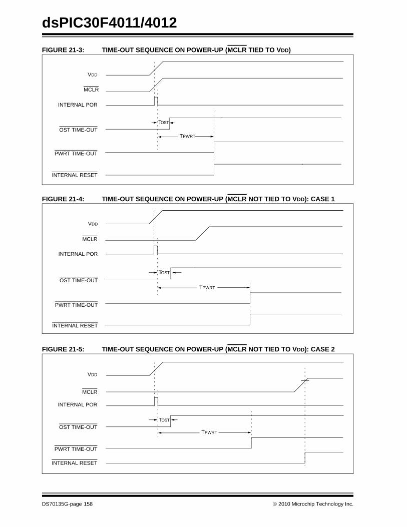
dsPIC30F4011/4012
FIGURE 21-3: TIME-OUT SEQUENCE ON POWER-UP (MCLR TIED TO VDD)FIGURE 21-4: TIME-OUT SEQUENCE ON POWER-UP (MCLR NOT TIED TO VDD): CASE 1
FIGURE 21-5: TIME-OUT SEQUENCE ON POWER-UP (MCLR NOT TIED TO VDD): CASE 2
TPWRT
TOST
VDD
INTERNAL POR
PWRT TIME-OUT
OST TIME-OUT
INTERNAL RESET
MCLR
TPWRT
TOST
VDD
INTERNAL POR
PWRT TIME-OUT
OST TIME-OUT
INTERNAL RESET
MCLR
VDD
MCLR
INTERNAL POR
PWRT TIME-OUT
OST TIME-OUT
INTERNAL RESET
TPWRT
TOST
DS70135G-page 158 © 2010 Microchip Technology Inc.

dsPIC30F4011/4012
21.3.1.1 POR with Long Crystal Start-up Time(with FSCM Enabled)The oscillator start-up circuitry is not linked to the PORcircuitry. Some crystal circuits (especially low-frequency crystals) have a relatively long start-up time.Therefore, one or more of the following conditions ispossible after the POR timer and the PWRT haveexpired:
• The oscillator circuit has not begun to oscillate.• The Oscillator Start-up Timer has not expired (if a
crystal oscillator is used).• The PLL has not achieved a lock (if PLL is used).
If the FSCM is enabled and one of the above conditionsis true, then a clock failure trap occurs. The deviceautomatically switches to the FRC oscillator and theuser can switch to the desired crystal oscillator in thetrap ISR.
21.3.1.2 Operating without FSCM and PWRTIf the FSCM is disabled and the Power-up Timer(PWRT) is also disabled, then the device exits rapidlyfrom Reset on power-up. If the clock source is FRC,LPRC, ERC or EC, it will be active immediately.
If the FSCM is disabled and the system clock has notstarted, the device will be in a frozen state at the Resetvector until the system clock starts. From the user’sperspective, the device will appear to be in Reset untila system clock is available.
21.3.2 BOR: PROGRAMMABLE BROWN-OUT RESET
The BOR (Brown-out Reset) module is based on aninternal voltage reference circuit. The main purpose ofthe BOR module is to generate a device Reset when abrown-out condition occurs. Brown-out conditions aregenerally caused by glitches on the AC mains (i.e.,missing portions of the AC cycle waveform due to badpower transmission lines, or voltage sags due to exces-sive current draw when a large inductive load is turnedon).
The BOR module allows selection of one of thefollowing voltage trip points (see Table 24-10):
• 2.6V-2.71V• 4.1V-4.4V• 4.58V-4.73V
A BOR generates a Reset pulse, which resets thedevice. The BOR selects the clock source, based onthe device Configuration bit values (FOS<1:0> andFPR<3:0>). Furthermore, if an oscillator mode isselected, the BOR activates the Oscillator Start-upTimer (OST). The system clock is held until OSTexpires. If the PLL is used, then the clock is held untilthe LOCK bit (OSCCON<5>) is ‘1’.
Concurrently, the POR time-out (TPOR) and the PWRTtime-out (TPWRT) are applied before the internal Resetis released. If TPWRT = 0 and a crystal oscillator isbeing used, then a nominal delay of TFSCM = 100 μs isapplied. The total delay in this case is (TPOR + TFSCM).
The BOR status bit (RCON<1>) is set to indicate that aBOR has occurred. The BOR circuit, if enabled, contin-ues to operate while in Sleep or Idle modes and resetsthe device if VDD falls below the BOR threshold voltage.
FIGURE 21-6: EXTERNAL POWER-ON RESET CIRCUIT (FOR SLOW VDD POWER-UP)
Note: The BOR voltage trip points indicated hereare nominal values provided for designguidance only.
Note: Dedicated supervisory devices, such asthe MCP1XX and MCP8XX, may also beused as an external Power-on Resetcircuit.
Note 1: External Power-on Reset circuit is requiredonly if the VDD power-up slope is too slow.The diode D helps discharge the capacitorquickly when VDD powers down.
2: R should be suitably chosen so as to makesure that the voltage drop across R does notviolate the device’s electrical specification.
3: R1 should be suitably chosen so as to limitany current flowing into MCLR from externalcapacitor C, in the event of MCLR pin break-down, due to Electrostatic Discharge (ESD)or Electrical Overstress (EOS).
C
R1RD
VDD
dsPIC30FMCLR
© 2010 Microchip Technology Inc. DS70135G-page 159

dsPIC30F4011/4012
Table 21-5 lists the Reset conditions for the RCONRegister. Since the control bits within the RCON regis-ter are R/W, the information in the table implies that allthe bits are negated prior to the action specified in thecondition column.TABLE 21-5: INITIALIZATION CONDITION FOR RCON REGISTER, CASE 1
Table 21-6 lists a second example of the bitconditions for the RCON register. In this case, it is notassumed that the user has set/cleared specific bitsprior to action specified in the condition column.
TABLE 21-6: INITIALIZATION CONDITION FOR RCON REGISTER, CASE 2
Condition Program Counter TRAPR IOPUWR EXTR SWR WDTO IDLE SLEEP POR BOR
Power-on Reset 0x000000 0 0 0 0 0 0 0 1 1
Brown-out Reset 0x000000 0 0 0 0 0 0 0 0 1
MCLR Reset during normal operation
0x000000 0 0 1 0 0 0 0 0 0
Software Reset during normal operation
0x000000 0 0 0 1 0 0 0 0 0
MCLR Reset during Sleep 0x000000 0 0 1 0 0 0 1 0 0
MCLR Reset during Idle 0x000000 0 0 1 0 0 1 0 0 0
WDT Time-out Reset 0x000000 0 0 0 0 1 0 0 0 0
WDT Wake-up PC + 2 0 0 0 0 1 0 1 0 0
Interrupt Wake-up from Sleep
PC + 2(1) 0 0 0 0 0 0 1 0 0
Clock Failure Trap 0x000004 0 0 0 0 0 0 0 0 0
Trap Reset 0x000000 1 0 0 0 0 0 0 0 0
Illegal Operation Trap 0x000000 0 1 0 0 0 0 0 0 0
Note 1: When the wake-up is due to an enabled interrupt, the PC is loaded with the corresponding interrupt vector.
Condition Program Counter TRAPR IOPUWR EXTR SWR WDTO IDLE SLEEP POR BOR
Power-on Reset 0x000000 0 0 0 0 0 0 0 1 1
Brown-out Reset 0x000000 u u u u u u u 0 1
MCLR Reset during normal operation
0x000000 u u 1 0 0 0 0 u u
Software Reset during normal operation
0x000000 u u 0 1 0 0 0 u u
MCLR Reset during Sleep 0x000000 u u 1 u 0 0 1 u u
MCLR Reset during Idle 0x000000 u u 1 u 0 1 0 u u
WDT Time-out Reset 0x000000 u u 0 0 1 0 0 u u
WDT Wake-up PC + 2 u u u u 1 u 1 u u
Interrupt Wake-up from Sleep
PC + 2(1) u u u u u u 1 u u
Clock Failure Trap 0x000004 u u u u u u u u u
Trap Reset 0x000000 1 u u u u u u u u
Illegal Operation Reset 0x000000 u 1 u u u u u u u
Legend: u = unchangedNote 1: When the wake-up is due to an enabled interrupt, the PC is loaded with the corresponding interrupt vector.
DS70135G-page 160 © 2010 Microchip Technology Inc.

dsPIC30F4011/4012
21.4 Watchdog Timer (WDT)21.4.1 WATCHDOG TIMER OPERATIONThe primary function of the Watchdog Timer (WDT) isto reset the processor in the event of a softwaremalfunction. The WDT is a free-running timer that runsoff an on-chip RC oscillator, requiring no externalcomponent. Therefore, the WDT timer continues tooperate even if the main processor clock (e.g., thecrystal oscillator) fails.
21.4.2 ENABLING AND DISABLING THE WDT
The Watchdog Timer can be “Enabled” or “Disabled”only through a Configuration bit (FWDTEN) in theConfiguration register, FWDT.
Setting FWDTEN = 1 enables the Watchdog Timer.The enabling is done when programming the device.By default, after chip erase, FWDTEN bit = 1. Anydevice programmer capable of programmingdsPIC30F devices allows programming of this andother Configuration bits.
If enabled, the WDT increments until it overflows or“times out”. A WDT time-out forces a device Reset(except during Sleep). To prevent a WDT time-out, theuser must clear the Watchdog Timer using a CLRWDTinstruction.
If a WDT times out during Sleep, the device wakes-up.The WDTO bit in the RCON register is cleared toindicate a wake-up resulting from a WDT time-out.
Setting FWDTEN = 0 allows user software to enable/disable the Watchdog Timer via the SWDTEN(RCON<5>) control bit.
21.5 Power-Saving ModesThere are two power-saving states that can be enteredthrough the execution of a special instruction, PWRSAV.
These are: Sleep and Idle.
The format of the PWRSAV instruction is as follows:
PWRSAV <parameter>
where,
‘parameter’ defines Idle or Sleep mode.
21.5.1 SLEEP MODE In Sleep mode, the clock to the CPU and peripherals isshut down. If an on-chip oscillator is being used, it isshut down.
The Fail-Safe Clock Monitor is not functional duringSleep, since there is no clock to monitor. However, theLPRC clock remains active if WDT is operational duringSleep.
The Brown-out Reset protection circuit and the Low-Voltage Detect (LVD) circuit, if enabled, remainfunctional during Sleep.
The processor wakes up from Sleep if at least one ofthe following conditions has occurred:
• Any interrupt that is individually enabled and meets the required priority level
• Any Reset (POR, BOR and MCLR) • WDT time-out
On waking up from Sleep mode, the processor restartsthe same clock that was active prior to entry into Sleepmode. When clock switching is enabled, bitsCOSC<1:0> determine the oscillator source to beused on wake-up. If clock switch is disabled, thenthere is only one system clock.
If the clock source is an oscillator, the clock to thedevice is held off until OST times out (indicating astable oscillator). If PLL is used, the system clock isheld off until LOCK = 1 (indicating that the PLL isstable). In either case, TPOR, TLOCK and TPWRT delaysare applied.
If EC, FRC, LPRC or ERC oscillators are used, then adelay of TPOR (~10 μs) is applied. This is the smallestdelay possible on wake-up from Sleep.
Moreover, if the LP oscillator was active during Sleep,and LP is the oscillator used on wake-up, then the start-up delay is equal to TPOR. PWRT and OST delays arenot applied. In order to have the smallest possible start-up delay when waking up from Sleep, one of thesefaster wake-up options should be selected beforeentering Sleep.
Note: If a POR or BOR occurred, the selection ofthe oscillator is based on the FOS<1:0>and FPR<3:0> Configuration bits.
© 2010 Microchip Technology Inc. DS70135G-page 161

dsPIC30F4011/4012
Any interrupt that is individually enabled (using thecorresponding IE bit) and meets the prevailing prioritylevel can wake-up the processor. The processorprocesses the interrupt and branches to the ISR. TheSLEEP status bit in the RCON register is set uponwake-up.All Resets wake-up the processor from Sleep mode.Any Reset, other than POR, sets the SLEEP status bit.In a POR, the SLEEP bit is cleared.
If Watchdog Timer is enabled, the processor wakes-upfrom Sleep mode upon WDT time-out. The SLEEP andWDTO status bits are both set.
21.5.2 IDLE MODEIn Idle mode, the clock to the CPU is shut down whileperipherals keep running. Unlike Sleep mode, the clocksource remains active.
Several peripherals have a control bit in each module,that allows them to operate during Idle.
LPRC Fail-Safe Clock Monitor remains active if clockfailure detect is enabled.
The processor wakes up from Idle if at least one of thefollowing conditions is true:
• Any interrupt that is individually enabled (IE bit is ‘1’) and meets the required priority level
• Any Reset (POR, BOR, MCLR)• WDT time-out
Upon wake-up from Idle mode, the clock is re-appliedto the CPU and instruction execution beginsimmediately, starting with the instruction following thePWRSAV instruction.
Any interrupt that is individually enabled (using IE bit)and meets the prevailing priority level can wake-up theprocessor. The processor processes the interrupt andbranches to the ISR. The IDLE status bit in RCONregister is set upon wake-up.
Any Reset, other than POR, sets the IDLE status bit.On a POR, the IDLE bit is cleared.
If Watchdog Timer is enabled, then the processorwakes-up from Idle mode upon WDT time-out. TheIDLE and WDTO status bits are both set.
Unlike wake-up from Sleep, there are no time delaysinvolved in wake-up from Idle.
21.6 Device Configuration RegistersThe Configuration bits in each device Configurationregister specify some of the device modes and areprogrammed by a device programmer, or by using theIn-Circuit Serial Programming™ (ICSP™) feature of thedevice. Each device Configuration register is a 24-bitregister, but only the lower 16 bits of each register areused to hold configuration data. There are five deviceConfiguration registers available to the user:
1. FOSC (0xF80000): Oscillator Configuration Register
2. FWDT (0xF80002): Watchdog Timer Configuration Register
3. FBORPOR (0xF80004): BOR and POR Configuration Register
4. FGS (0xF8000A): General Code Segment Configuration Register
5. FICD (0xF8000C): Debug Configuration Register
The placement of the Configuration bits is automaticallyhandled when you select the device in your deviceprogrammer. The desired state of the Configuration bitsmay be specified in the source code (dependent on thelanguage tool used), or through the programminginterface. After the device has been programmed, theapplication software may read the Configuration bitvalues through the table read instructions. For additionalinformation, please refer to the programmingspecifications of the device.
Note: In spite of various delays applied (TPOR,TLOCK and TPWRT), the crystal oscillator(and PLL) may not be active at the end ofthe time-out (e.g., for low-frequency crys-tals). In such cases, if FSCM is enabled,the device detects this condition as aclock failure and processes the clock fail-ure trap. The FRC oscillator is enabled,and the user must re-enable the crystaloscillator. If FSCM is not enabled, then thedevice simply suspends execution of codeuntil the clock is stable and remains inSleep until the oscillator clock has started.
Note: If the code protection Configuration fusebits (FGS<GCP> and FGS<GWRP>)have been programmed, an erase of theentire code-protected device is onlypossible at voltages VDD ≥ 4.5V.
DS70135G-page 162 © 2010 Microchip Technology Inc.

dsPIC30F4011/4012
21.7 In-Circuit DebuggerWhen MPLAB® ICD 2 is selected as a debugger, thein-circuit debugging functionality is enabled. This func-tion allows simple debugging functions when used withMPLAB IDE. When the device has this feature enabled,some of the resources are not available for generaluse. These resources include the first 80 bytes of dataRAM and two I/O pins.one of four pairs of debug I/O pins may be selected bythe user using configuration options in MPLAB IDE.These pin pairs are named EMUD/EMUC, EMUD1/EMUC1, EMUD2/EMUC2 and EMUD3/EMUC3.
In each case, the selected EMUD pin is the emulation/debug data line and the EMUC pin is the emulation/debug clock line. These pins interface to the MPLABICD 2 module available from Microchip. The selectedpair of debug I/O pins is used by MPLAB ICD 2 to sendcommands and receive responses, as well as to sendand receive data. To use the in-circuit debugger func-tion of the device, the design must implement ICSPconnections to MCLR, VDD, VSS, PGC, PGD and theselected EMUDx/EMUCx pin pair.
This gives rise to two possibilities:
1. If EMUD/EMUC is selected as the debug I/O pinpair, then only a 5-pin interface is required as theEMUD and EMUC pin functions are multiplexedwith the PGD and PGC pin functions in alldsPIC30F devices.
2. If EMUD1/EMUC1, EMUD2/EMUC2 or EMUD3/EMUC3 is selected as the debug I/O pin pair,then a 7-pin interface is required as the EMUDx/EMUCx pin functions (x = 1, 2 or 3) are notmultiplexed with the PGD and PGC pinfunctions.
© 2010 Microchip Technology Inc. DS70135G-page 163

dsPIC30F4011/4012
DS
70135G-page 164
© 2010 M
icrochip Technology Inc.
Bit 1 Bit 0 Reset State
BOR POR Depends on type of Reset.
LPOSCEN OSWEN Depends on Configuration bits.
Bit 4 Bit 3 Bit 2 Bit 1 Bit 0
— FPR<3:0>
<1:0> FWPSB<3:0>
<1:0> — — FPWRT<1:0>
— Reserved(2)
— Reserved(2)
— — Reserved(2) GCP GWRP
— — — ICS<1:0>
TABLE 21-7: SYSTEM INTEGRATION REGISTER MAP(1)
TABLE 21-8: DEVICE CONFIGURATION REGISTER MAP(1)
SFR Name Addr. Bit 15 Bit 14 Bit 13 Bit 12 Bit 11 Bit 10 Bit 9 Bit 8 Bit 7 Bit 6 Bit 5 Bit 4 Bit 3 Bit 2
RCON 0740 TRAPR IOPUWR BGST — EXTR SWR SWDTEN WDTO SLEEP IDLE
OSCCON 0742 TUN3 TUN2 COSC<1:0> TUN1 TUN0 NOSC<1:0> POST<1:0> LOCK — CF —
Legend: — = unimplemented bit, read as ‘0’Note 1: Refer to the “dsPIC30F Family Reference Manual” (DS70046) for descriptions of register bit fields.
Name Address Bit 15 Bit 14 Bit 13 Bit 12 Bit 11 Bit 10 Bit 9 Bit 8 Bit 7 Bit 6 Bit 5
FOSC F80000 FCKSM<1:0> — — — — FOS<1:0> — — —
FWDT F80002 FWDTEN — — — — — — — — — FWPSA
FBORPOR F80004 MCLREN — — — — PWMPIN HPOL LPOL BOREN — BORV
FBS F80006 — — Reserved(2) — — — Reserved(2) — — —
FSS F80008 — — Reserved(2) — — Reserved(2) — — —
FGS F8000A — — — — — — — — — — —
FICD F8000C BKBUG COE — — — — — — — — —
Legend: — = unimplemented bit, read as ‘0’Note 1: Refer to the “dsPIC30F Family Reference Manual” (DS70046) for descriptions of register bit fields.
2: Reserved bits read as ‘1’ and must be programmed as ‘1’.

dsPIC30F4011/4012
22.0 INSTRUCTION SET SUMMARY
The dsPIC30F instruction set adds manyenhancements to the previous PIC® MCU instructionsets, while maintaining an easy migration from PICMCU instruction sets.
Most instructions are a single program memory word(24 bits). Only three instructions require two programmemory locations.
Each single-word instruction is a 24-bit word dividedinto an 8-bit opcode, which specifies the instructiontype, and one or more operands which further specifythe operation of the instruction.
The instruction set is highly orthogonal and is groupedinto five basic categories:
• Word or byte-oriented operations• Bit-oriented operations• Literal operations• DSP operations• Control operations
Table 22-1 shows the general symbols used indescribing the instructions.
The dsPIC30F instruction set summary in Table 22-2lists all the instructions along with the status flagsaffected by each instruction.
Most word or byte-oriented W register instructions(including barrel shift instructions) have threeoperands:
• The first source operand, which is typically a register ‘Wb’ without any address modifier
• The second source operand, which is typically a register ‘Ws’ with or without an address modifier
• The destination of the result, which is typically a register ‘Wd’ with or without an address modifier
However, word or byte-oriented file register instructionshave two operands:
• The file register specified by the value ‘f’• The destination, which could either be the file
register ‘f’ or the W0 register, which is denoted as ‘WREG’
Most bit-oriented instructions (including simple rotate/shift instructions) have two operands:
• The W register (with or without an address modi-fier) or file register (specified by the value of ‘Ws’ or ‘f’)
• The bit in the W register or file register (specified by a literal value or indirectly by the contents of register ‘Wb’)
The literal instructions that involve data movement mayuse some of the following operands:
• A literal value to be loaded into a W register or file register (specified by the value of ‘k’)
• The W register or file register where the literal value is to be loaded (specified by ‘Wb’ or ‘f’)
However, literal instructions that involve arithmetic orlogical operations use some of the following operands:
• The first source operand which is a register ‘Wb’ without any address modifier
• The second source operand which is a literal value
• The destination of the result (only if not the same as the first source operand) which is typically a register ‘Wd’ with or without an address modifier
The MAC class of DSP instructions may use some of thefollowing operands:
• The accumulator (A or B) to be used (required operand)
• The W registers to be used as the two operands• The X and Y address space prefetch operations• The X and Y address space prefetch destinations• The accumulator write-back destination
The other DSP instructions do not involve anymultiplication and may include:
• The accumulator to be used (required)• The source or destination operand (designated as
Wso or Wdo, respectively) with or without an address modifier
• The amount of shift, specified by a W register ‘Wn’ or a literal value
The control instructions may use some of the followingoperands:
• A program memory address • The mode of the table read and table write
instructions
All instructions are a single word, except for certaindouble-word instructions, which were made double-word instructions so that all the required information isavailable in these 48 bits. In the second word, the8 MSbs are ‘0’s. If this second word is executed as aninstruction (by itself), it will execute as a NOP.
Note: This data sheet summarizes features ofthis group of dsPIC30F devices and is notintended to be a complete referencesource. For more information on the CPU,peripherals, register descriptions andgeneral device functionality, refer to thedsPIC30F Family Reference Manual(DS70046). For more information on thedevice instruction set and programming,refer to the “16-bit MCU and DSCReference Manual” (DS70157).
© 2010 Microchip Technology Inc. DS70135G-page 165
dsPIC30F4011/4012
Most single-word instructions are executed in a singleinstruction cycle, unless a conditional test is true or theprogram counter is changed as a result of the instruc-tion. In these cases, the execution takes two instructioncycles with the additional instruction cycle(s) executedas a NOP. Notable exceptions are the BRA (uncondi-tional/computed branch), indirect CALL/GOTO, all tablereads and writes and RETURN/RETFIE instructions,which are single-word instructions but take two or threecycles. Certain instructions that involve skipping overthe subsequent instruction, require either two or threecycles if the skip is performed, depending on whetherthe instruction being skipped is a single-word or two-word instruction. Moreover, double-word movesrequire two cycles. The double-word instructionsexecute in two instruction cycles.Note: For more details on the instruction set,refer to the “16-bit MCU and DSCReference Manual” (DS70157).
TABLE 22-1: SYMBOLS USED IN OPCODE DESCRIPTIONSField Description
#text Means literal defined by “text“(text) Means “content of text“[text] Means “the location addressed by text”{ } Optional field or operation<n:m> Register bit field.b Byte mode selection.d Double-Word mode selection.S Shadow register select.w Word mode selection (default)Acc One of two accumulators {A, B}AWB Accumulator Write-Back Destination Address register ∈ {W13, [W13]+=2}bit4 4-bit bit selection field (used in word addressed instructions) ∈ {0...15}C, DC, N, OV, Z MCU Status bits: Carry, Digit Carry, Negative, Overflow, ZeroExpr Absolute address, label or expression (resolved by the linker)f File register address ∈ {0x0000...0x1FFF}lit1 1-bit unsigned literal ∈ {0,1}lit4 4-bit unsigned literal ∈ {0...15}lit5 5-bit unsigned literal ∈ {0...31}lit8 8-bit unsigned literal ∈ {0...255}lit10 10-bit unsigned literal ∈ {0...255} for Byte mode, {0:1023} for Word modelit14 14-bit unsigned literal ∈ {0...16384}lit16 16-bit unsigned literal ∈ {0...65535}lit23 23-bit unsigned literal ∈ {0...8388608}; LSB must be 0None Field does not require an entry, may be blankOA, OB, SA, SB DSP Status bits: ACCA Overflow, ACCB Overflow, ACCA Saturate, ACCB SaturatePC Program CounterSlit10 10-bit signed literal ∈ {-512...511}Slit16 16-bit signed literal ∈ {-32768...32767}Slit6 6-bit signed literal ∈ {-16...16}
DS70135G-page 166 © 2010 Microchip Technology Inc.
dsPIC30F4011/4012
Wb Base W register ∈ {W0..W15}Wd Destination W register ∈ { Wd, [Wd], [Wd++], [Wd--], [++Wd], [--Wd] }Wdo Destination W register ∈
{ Wnd, [Wnd], [Wnd++], [Wnd--], [++Wnd], [--Wnd], [Wnd+Wb] } Wm,Wn Dividend, Divisor working register pair (Direct Addressing)Wm*Wm Multiplicand and Multiplier working register pair for Square instructions ∈
{W4*W4, W5*W5, W6*W6, W7*W7} Wm*Wn Multiplicand and Multiplier working register pair for DSP instructions ∈
{W4*W5, W4*W6, W4*W7, W5*W6, W5*W7, W6*W7}Wn One of 16 working registers ∈ {W0..W15}Wnd One of 16 destination working registers ∈ {W0..W15}Wns One of 16 source working registers ∈ {W0..W15}WREG W0 (working register used in file register instructions)Ws Source W register ∈ { Ws, [Ws], [Ws++], [Ws--], [++Ws], [--Ws] }Wso Source W register ∈
{ Wns, [Wns], [Wns++], [Wns--], [++Wns], [--Wns], [Wns+Wb] } Wx X Data Space Prefetch Address register for DSP instructions
∈ {[W8]+=6, [W8]+=4, [W8]+=2, [W8], [W8]-=6, [W8]-=4, [W8]-=2, [W9]+=6, [W9]+=4, [W9]+=2, [W9], [W9]-=6, [W9]-=4, [W9]-=2, [W9+W12],none}
Wxd X Data Space Prefetch Destination register for DSP instructions ∈ {W4..W7}Wy Y Data Space Prefetch Address register for DSP instructions
∈ {[W10]+=6, [W10]+=4, [W10]+=2, [W10], [W10]-=6, [W10]-=4, [W10]-=2, [W11]+=6, [W11]+=4, [W11]+=2, [W11], [W11]-=6, [W11]-=4, [W11]-=2, [W11+W12], none}
Wyd Y Data Space Prefetch Destination register for DSP instructions ∈ {W4..W7}
TABLE 22-1: SYMBOLS USED IN OPCODE DESCRIPTIONS (CONTINUED)Field Description
© 2010 Microchip Technology Inc. DS70135G-page 167

dsPIC30F4011/4012
TABLE 22-2: INSTRUCTION SET OVERVIEWBaseInstr
#
AssemblyMnemonic Assembly Syntax Description # of
words# of
cyclesStatus Flags
Affected
1 ADD ADD Acc Add Accumulators 1 1 OA, OB, SA, SB
ADD f f = f + WREG 1 1 C, DC, N, OV, Z
ADD f,WREG WREG = f + WREG 1 1 C, DC, N, OV, Z
ADD #lit10,Wn Wd = lit10 + Wd 1 1 C, DC, N, OV, Z
ADD Wb,Ws,Wd Wd = Wb + Ws 1 1 C, DC, N, OV, Z
ADD Wb,#lit5,Wd Wd = Wb + lit5 1 1 C, DC, N, OV, Z
ADD Wso,#Slit4,Acc 16-bit Signed Add to Accumulator 1 1 OA, OB, SA, SB
2 ADDC ADDC f f = f + WREG + (C) 1 1 C, DC, N, OV, Z
ADDC f,WREG WREG = f + WREG + (C) 1 1 C, DC, N, OV, Z
ADDC #lit10,Wn Wd = lit10 + Wd + (C) 1 1 C, DC, N, OV, Z
ADDC Wb,Ws,Wd Wd = Wb + Ws + (C) 1 1 C, DC, N, OV, Z
ADDC Wb,#lit5,Wd Wd = Wb + lit5 + (C) 1 1 C, DC, N, OV, Z
3 AND AND f f = f .AND. WREG 1 1 N, Z
AND f,WREG WREG = f .AND. WREG 1 1 N, Z
AND #lit10,Wn Wd = lit10 .AND. Wd 1 1 N, Z
AND Wb,Ws,Wd Wd = Wb .AND. Ws 1 1 N, Z
AND Wb,#lit5,Wd Wd = Wb .AND. lit5 1 1 N, Z
4 ASR ASR f f = Arithmetic Right Shift f 1 1 C, N, OV, Z
ASR f,WREG WREG = Arithmetic Right Shift f 1 1 C, N, OV, Z
ASR Ws,Wd Wd = Arithmetic Right Shift Ws 1 1 C, N, OV, Z
ASR Wb,Wns,Wnd Wnd = Arithmetic Right Shift Wb by Wns 1 1 N, Z
ASR Wb,#lit5,Wnd Wnd = Arithmetic Right Shift Wb by lit5 1 1 N, Z
5 BCLR BCLR f,#bit4 Bit Clear f 1 1 None
BCLR Ws,#bit4 Bit Clear Ws 1 1 None
6 BRA BRA C,Expr Branch if Carry 1 1 (2) None
BRA GE,Expr Branch if greater than or equal 1 1 (2) None
BRA GEU,Expr Branch if unsigned greater than or equal 1 1 (2) None
BRA GT,Expr Branch if greater than 1 1 (2) None
BRA GTU,Expr Branch if unsigned greater than 1 1 (2) None
BRA LE,Expr Branch if less than or equal 1 1 (2) None
BRA LEU,Expr Branch if unsigned less than or equal 1 1 (2) None
BRA LT,Expr Branch if less than 1 1 (2) None
BRA LTU,Expr Branch if unsigned less than 1 1 (2) None
BRA N,Expr Branch if Negative 1 1 (2) None
BRA NC,Expr Branch if Not Carry 1 1 (2) None
BRA NN,Expr Branch if Not Negative 1 1 (2) None
BRA NOV,Expr Branch if Not Overflow 1 1 (2) None
BRA NZ,Expr Branch if Not Zero 1 1 (2) None
BRA OA,Expr Branch if Accumulator A overflow 1 1 (2) None
BRA OB,Expr Branch if Accumulator B overflow 1 1 (2) None
BRA OV,Expr Branch if Overflow 1 1 (2) None
BRA SA,Expr Branch if Accumulator A saturated 1 1 (2) None
BRA SB,Expr Branch if Accumulator B saturated 1 1 (2) None
BRA Expr Branch Unconditionally 1 2 None
BRA Z,Expr Branch if Zero 1 1 (2) None
BRA Wn Computed Branch 1 2 None
7 BSET BSET f,#bit4 Bit Set f 1 1 None
BSET Ws,#bit4 Bit Set Ws 1 1 None
8 BSW BSW.C Ws,Wb Write C bit to Ws<Wb> 1 1 None
BSW.Z Ws,Wb Write Z bit to Ws<Wb> 1 1 None
DS70135G-page 168 © 2010 Microchip Technology Inc.

dsPIC30F4011/4012
9 BTG BTG f,#bit4 Bit Toggle f 1 1 None
BTG Ws,#bit4 Bit Toggle Ws 1 1 None
10 BTSC BTSC f,#bit4 Bit Test f, Skip if Clear 1 1 (2 or 3)
None
BTSC Ws,#bit4 Bit Test Ws, Skip if Clear 1 1 (2 or 3)
None
11 BTSS BTSS f,#bit4 Bit Test f, Skip if Set 1 1 (2 or 3)
None
BTSS Ws,#bit4 Bit Test Ws, Skip if Set 1 1 (2 or 3)
None
12 BTST BTST f,#bit4 Bit Test f 1 1 Z
BTST.C Ws,#bit4 Bit Test Ws to C 1 1 C
BTST.Z Ws,#bit4 Bit Test Ws to Z 1 1 Z
BTST.C Ws,Wb Bit Test Ws<Wb> to C 1 1 C
BTST.Z Ws,Wb Bit Test Ws<Wb> to Z 1 1 Z
13 BTSTS BTSTS f,#bit4 Bit Test then Set f 1 1 Z
BTSTS.C Ws,#bit4 Bit Test Ws to C, then Set 1 1 C
BTSTS.Z Ws,#bit4 Bit Test Ws to Z, then Set 1 1 Z
14 CALL CALL lit23 Call subroutine 2 2 None
CALL Wn Call indirect subroutine 1 2 None
15 CLR CLR f f = 0x0000 1 1 None
CLR WREG WREG = 0x0000 1 1 None
CLR Ws Ws = 0x0000 1 1 None
CLR Acc,Wx,Wxd,Wy,Wyd,AWB Clear Accumulator 1 1 OA, OB, SA, SB
16 CLRWDT CLRWDT Clear Watchdog Timer 1 1 WDTO, Sleep
17 COM COM f f = f 1 1 N, Z
COM f,WREG WREG = f 1 1 N, Z
COM Ws,Wd Wd = Ws 1 1 N, Z
18 CP CP f Compare f with WREG 1 1 C, DC, N, OV, Z
CP Wb,#lit5 Compare Wb with lit5 1 1 C, DC, N, OV, Z
CP Wb,Ws Compare Wb with Ws (Wb – Ws) 1 1 C, DC, N, OV, Z
19 CP0 CP0 f Compare f with 0x0000 1 1 C, DC, N, OV, Z
CP0 Ws Compare Ws with 0x0000 1 1 C, DC, N, OV, Z
20 CPB CPB f Compare f with WREG, with Borrow 1 1 C, DC, N, OV, Z
CPB Wb,#lit5 Compare Wb with lit5, with Borrow 1 1 C, DC, N, OV, Z
CPB Wb,Ws Compare Wb with Ws, with Borrow(Wb – Ws – C)
1 1 C, DC, N, OV, Z
21 CPSEQ CPSEQ Wb, Wn Compare Wb with Wn, skip if = 1 1 (2 or 3)
None
22 CPSGT CPSGT Wb, Wn Compare Wb with Wn, skip if > 1 1 (2 or 3)
None
23 CPSLT CPSLT Wb, Wn Compare Wb with Wn, skip if < 1 1 (2 or 3)
None
24 CPSNE CPSNE Wb, Wn Compare Wb with Wn, skip if ≠ 1 1 (2 or 3)
None
25 DAW DAW Wn Wn = decimal adjust Wn 1 1 C
26 DEC DEC f f = f –1 1 1 C, DC, N, OV, Z
DEC f,WREG WREG = f –1 1 1 C, DC, N, OV, Z
DEC Ws,Wd Wd = Ws – 1 1 1 C, DC, N, OV, Z
27 DEC2 DEC2 f f = f – 2 1 1 C, DC, N, OV, Z
DEC2 f,WREG WREG = f – 2 1 1 C, DC, N, OV, Z
DEC2 Ws,Wd Wd = Ws – 2 1 1 C, DC, N, OV, Z
28 DISI DISI #lit14 Disable Interrupts for k instruction cycles 1 1 None
TABLE 22-2: INSTRUCTION SET OVERVIEW (CONTINUED)BaseInstr
#
AssemblyMnemonic Assembly Syntax Description # of
words# of
cyclesStatus Flags
Affected
© 2010 Microchip Technology Inc. DS70135G-page 169

dsPIC30F4011/4012
29 DIV DIV.S Wm,Wn Signed 16/16-bit Integer Divide 1 18 N, Z, C, OV
DIV.SD Wm,Wn Signed 32/16-bit Integer Divide 1 18 N, Z, C, OV
DIV.U Wm,Wn Unsigned 16/16-bit Integer Divide 1 18 N, Z, C, OV
DIV.UD Wm,Wn Unsigned 32/16-bit Integer Divide 1 18 N, Z, C, OV
30 DIVF DIVF Wm,Wn Signed 16/16-bit Fractional Divide 1 18 N, Z, C, OV
31 DO DO #lit14,Expr Do code to PC + Expr, lit14 + 1 time 2 2 None
DO Wn,Expr Do code to PC + Expr, (Wn) +1 time 2 2 None
32 ED ED Wm*Wm,Acc,Wx,Wy,Wxd Euclidean Distance ( no accumulate) 1 1 OA, OB, OAB,SA, SB, SAB
33 EDAC EDAC Wm*Wm,Acc,Wx,Wy,Wxd Euclidean Distance 1 1 OA, OB, OAB,SA, SB, SAB
34 EXCH EXCH Wns,Wnd Swap Wns with Wnd 1 1 None
35 FBCL FBCL Ws,Wnd Find Bit Change from Left (MSb) Side 1 1 C
36 FF1L FF1L Ws,Wnd Find First One from Left (MSb) Side 1 1 C
37 FF1R FF1R Ws,Wnd Find First One from Right (LSb) Side 1 1 C
38 GOTO GOTO Expr Go to address 2 2 None
GOTO Wn Go to indirect 1 2 None
39 INC INC f f = f + 1 1 1 C, DC, N, OV, Z
INC f,WREG WREG = f + 1 1 1 C, DC, N, OV, Z
INC Ws,Wd Wd = Ws + 1 1 1 C, DC, N, OV, Z
40 INC2 INC2 f f = f + 2 1 1 C, DC, N, OV, Z
INC2 f,WREG WREG = f + 2 1 1 C, DC, N, OV, Z
INC2 Ws,Wd Wd = Ws + 2 1 1 C, DC, N, OV, Z
41 IOR IOR f f = f .IOR. WREG 1 1 N, Z
IOR f,WREG WREG = f .IOR. WREG 1 1 N, Z
IOR #lit10,Wn Wd = lit10 .IOR. Wd 1 1 N, Z
IOR Wb,Ws,Wd Wd = Wb .IOR. Ws 1 1 N, Z
IOR Wb,#lit5,Wd Wd = Wb .IOR. lit5 1 1 N, Z
42 LAC LAC Wso,#Slit4,Acc Load Accumulator 1 1 OA, OB, OAB,SA, SB, SAB
43 LNK LNK #lit14 Link Frame Pointer 1 1 None
44 LSR LSR f f = Logical Right Shift f 1 1 C, N, OV, Z
LSR f,WREG WREG = Logical Right Shift f 1 1 C, N, OV, Z
LSR Ws,Wd Wd = Logical Right Shift Ws 1 1 C, N, OV, Z
LSR Wb,Wns,Wnd Wnd = Logical Right Shift Wb by Wns 1 1 N, Z
LSR Wb,#lit5,Wnd Wnd = Logical Right Shift Wb by lit5 1 1 N, Z
45 MAC MAC Wm*Wn,Acc,Wx,Wxd,Wy,Wyd,AWB
Multiply and Accumulate 1 1 OA, OB, OAB,SA, SB, SAB
MAC Wm*Wm,Acc,Wx,Wxd,Wy,Wyd Square and Accumulate 1 1 OA, OB, OAB,SA, SB, SAB
46 MOV MOV f,Wn Move f to Wn 1 1 None
MOV f Move f to f 1 1 None
MOV f,WREG Move f to WREG 1 1 None
MOV #lit16,Wn Move 16-bit literal to Wn 1 1 None
MOV.b #lit8,Wn Move 8-bit literal to Wn 1 1 None
MOV Wn,f Move Wn to f 1 1 None
MOV Wso,Wdo Move Ws to Wd 1 1 None
MOV WREG,f Move WREG to f 1 1 None
MOV.D Wns,Wd Move Double from W(ns):W(ns + 1) to Wd 1 2 None
MOV.D Ws,Wnd Move Double from Ws to W(nd + 1):W(nd) 1 2 None
47 MOVSAC MOVSAC Acc,Wx,Wxd,Wy,Wyd,AWB Prefetch and store accumulator 1 1 None
TABLE 22-2: INSTRUCTION SET OVERVIEW (CONTINUED)BaseInstr
#
AssemblyMnemonic Assembly Syntax Description # of
words# of
cyclesStatus Flags
Affected
DS70135G-page 170 © 2010 Microchip Technology Inc.

dsPIC30F4011/4012
48 MPY MPY Wm*Wn,Acc,Wx,Wxd,Wy,Wyd Multiply Wm by Wn to Accumulator 1 1 OA, OB, OAB,SA, SB, SAB
MPY Wm*Wm,Acc,Wx,Wxd,Wy,Wyd Square Wm to Accumulator 1 1 OA, OB, OAB,SA, SB, SAB
49 MPY.N MPY.N Wm*Wn,Acc,Wx,Wxd,Wy,Wyd -(Multiply Wm by Wn) to Accumulator 1 1 None
50 MSC MSC Wm*Wm,Acc,Wx,Wxd,Wy,Wyd,AWB
Multiply and Subtract from Accumulator 1 1 OA, OB, OAB,SA, SB, SAB
51 MUL MUL.SS Wb,Ws,Wnd {Wnd+1, Wnd} = signed(Wb) * signed(Ws) 1 1 None
MUL.SU Wb,Ws,Wnd {Wnd+1, Wnd} = signed(Wb) * unsigned(Ws) 1 1 None
MUL.US Wb,Ws,Wnd {Wnd+1, Wnd} = unsigned(Wb) * signed(Ws) 1 1 None
MUL.UU Wb,Ws,Wnd {Wnd+1, Wnd} = unsigned(Wb) * unsigned(Ws)
1 1 None
MUL.SU Wb,#lit5,Wnd {Wnd+1, Wnd} = signed(Wb) * unsigned(lit5) 1 1 None
MUL.UU Wb,#lit5,Wnd {Wnd+1, Wnd} = unsigned(Wb) * unsigned(lit5)
1 1 None
MUL f W3:W2 = f * WREG 1 1 None
52 NEG NEG Acc Negate Accumulator 1 1 OA, OB, OAB,SA, SB, SAB
NEG f f = f + 1 1 1 C, DC, N, OV, Z
NEG f,WREG WREG = f + 1 1 1 C, DC, N, OV, Z
NEG Ws,Wd Wd = Ws + 1 1 1 C, DC, N, OV, Z
53 NOP NOP No Operation 1 1 None
NOPR No Operation 1 1 None
54 POP POP f Pop f from Top-of-Stack (TOS) 1 1 None
POP Wdo Pop from Top-of-Stack (TOS) to Wdo 1 1 None
POP.D Wnd Pop from Top-of-Stack (TOS) to W(nd):W(nd +1)
1 2 None
POP.S Pop Shadow Registers 1 1 All
55 PUSH PUSH f Push f to Top-of-Stack (TOS) 1 1 None
PUSH Wso Push Wso to Top-of-Stack (TOS) 1 1 None
PUSH.D Wns Push W(ns):W(ns + 1) to Top-of-Stack (TOS) 1 2 None
PUSH.S Push Shadow Registers 1 1 None
56 PWRSAV PWRSAV #lit1 Go into Sleep or Idle mode 1 1 WDTO, Sleep
57 RCALL RCALL Expr Relative Call 1 2 None
RCALL Wn Computed Call 1 2 None
58 REPEAT REPEAT #lit14 Repeat Next Instruction lit14 + 1 time 1 1 None
REPEAT Wn Repeat Next Instruction (Wn) + 1 time 1 1 None
59 RESET RESET Software device Reset 1 1 None
60 RETFIE RETFIE Return from interrupt 1 3 (2) None
61 RETLW RETLW #lit10,Wn Return with literal in Wn 1 3 (2) None
62 RETURN RETURN Return from Subroutine 1 3 (2) None
63 RLC RLC f f = Rotate Left through Carry f 1 1 C, N, Z
RLC f,WREG WREG = Rotate Left through Carry f 1 1 C, N, Z
RLC Ws,Wd Wd = Rotate Left through Carry Ws 1 1 C, N, Z
64 RLNC RLNC f f = Rotate Left (No Carry) f 1 1 N, Z
RLNC f,WREG WREG = Rotate Left (No Carry) f 1 1 N, Z
RLNC Ws,Wd Wd = Rotate Left (No Carry) Ws 1 1 N, Z
65 RRC RRC f f = Rotate Right through Carry f 1 1 C, N, Z
RRC f,WREG WREG = Rotate Right through Carry f 1 1 C, N, Z
RRC Ws,Wd Wd = Rotate Right through Carry Ws 1 1 C, N, Z
TABLE 22-2: INSTRUCTION SET OVERVIEW (CONTINUED)BaseInstr
#
AssemblyMnemonic Assembly Syntax Description # of
words# of
cyclesStatus Flags
Affected
© 2010 Microchip Technology Inc. DS70135G-page 171
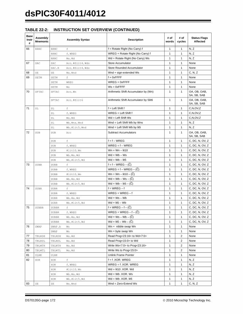
dsPIC30F4011/4012
66 RRNC RRNC f f = Rotate Right (No Carry) f 1 1 N, Z
RRNC f,WREG WREG = Rotate Right (No Carry) f 1 1 N, Z
RRNC Ws,Wd Wd = Rotate Right (No Carry) Ws 1 1 N, Z
67 SAC SAC Acc,#Slit4,Wdo Store Accumulator 1 1 None
SAC.R Acc,#Slit4,Wdo Store Rounded Accumulator 1 1 None
68 SE SE Ws,Wnd Wnd = sign-extended Ws 1 1 C, N, Z
69 SETM SETM f f = 0xFFFF 1 1 None
SETM WREG WREG = 0xFFFF 1 1 None
SETM Ws Ws = 0xFFFF 1 1 None
70 SFTAC SFTAC Acc,Wn Arithmetic Shift Accumulator by (Wn) 1 1 OA, OB, OAB,SA, SB, SAB
SFTAC Acc,#Slit6 Arithmetic Shift Accumulator by Slit6 1 1 OA, OB, OAB,SA, SB, SAB
71 SL SL f f = Left Shift f 1 1 C,N,OV,Z
SL f,WREG WREG = Left Shift f 1 1 C,N,OV,Z
SL Ws,Wd Wd = Left Shift Ws 1 1 C,N,OV,Z
SL Wb,Wns,Wnd Wnd = Left Shift Wb by Wns 1 1 N, Z
SL Wb,#lit5,Wnd Wnd = Left Shift Wb by lit5 1 1 N, Z
72 SUB SUB Acc Subtract Accumulators 1 1 OA, OB, OAB,SA, SB, SAB
SUB f f = f – WREG 1 1 C, DC, N, OV, Z
SUB f,WREG WREG = f – WREG 1 1 C, DC, N, OV, Z
SUB #lit10,Wn Wn = Wn – lit10 1 1 C, DC, N, OV, Z
SUB Wb,Ws,Wd Wd = Wb – Ws 1 1 C, DC, N, OV, Z
SUB Wb,#lit5,Wd Wd = Wb – lit5 1 1 C, DC, N, OV, Z
73 SUBB SUBB f f = f – WREG – (C) 1 1 C, DC, N, OV, Z
SUBB f,WREG WREG = f – WREG – (C) 1 1 C, DC, N, OV, Z
SUBB #lit10,Wn Wn = Wn – lit10 – (C) 1 1 C, DC, N, OV, Z
SUBB Wb,Ws,Wd Wd = Wb – Ws – (C) 1 1 C, DC, N, OV, Z
SUBB Wb,#lit5,Wd Wd = Wb – lit5 – (C) 1 1 C, DC, N, OV, Z
74 SUBR SUBR f f = WREG – f 1 1 C, DC, N, OV, Z
SUBR f,WREG WREG = WREG – f 1 1 C, DC, N, OV, Z
SUBR Wb,Ws,Wd Wd = Ws – Wb 1 1 C, DC, N, OV, Z
SUBR Wb,#lit5,Wd Wd = lit5 – Wb 1 1 C, DC, N, OV, Z
75 SUBBR SUBBR f f = WREG – f – (C) 1 1 C, DC, N, OV, Z
SUBBR f,WREG WREG = WREG – f – (C) 1 1 C, DC, N, OV, Z
SUBBR Wb,Ws,Wd Wd = Ws – Wb – (C) 1 1 C, DC, N, OV, Z
SUBBR Wb,#lit5,Wd Wd = lit5 – Wb – (C) 1 1 C, DC, N, OV, Z
76 SWAP SWAP.b Wn Wn = nibble swap Wn 1 1 None
SWAP Wn Wn = byte swap Wn 1 1 None
77 TBLRDH TBLRDH Ws,Wd Read Prog<23:16> to Wd<7:0> 1 2 None
78 TBLRDL TBLRDL Ws,Wd Read Prog<15:0> to Wd 1 2 None
79 TBLWTH TBLWTH Ws,Wd Write Ws<7:0> to Prog<23:16> 1 2 None
80 TBLWTL TBLWTL Ws,Wd Write Ws to Prog<15:0> 1 2 None
81 ULNK ULNK Unlink Frame Pointer 1 1 None
82 XOR XOR f f = f .XOR. WREG 1 1 N, Z
XOR f,WREG WREG = f .XOR. WREG 1 1 N, Z
XOR #lit10,Wn Wd = lit10 .XOR. Wd 1 1 N, Z
XOR Wb,Ws,Wd Wd = Wb .XOR. Ws 1 1 N, Z
XOR Wb,#lit5,Wd Wd = Wb .XOR. lit5 1 1 N, Z
83 ZE ZE Ws,Wnd Wnd = Zero-Extend Ws 1 1 C, N, Z
TABLE 22-2: INSTRUCTION SET OVERVIEW (CONTINUED)BaseInstr
#
AssemblyMnemonic Assembly Syntax Description # of
words# of
cyclesStatus Flags
Affected
DS70135G-page 172 © 2010 Microchip Technology Inc.
dsPIC30F4011/4012
23.0 DEVELOPMENT SUPPORTThe PIC® microcontrollers and dsPIC® digital signalcontrollers are supported with a full range of softwareand hardware development tools:
• Integrated Development Environment- MPLAB® IDE Software
• Compilers/Assemblers/Linkers- MPLAB C Compiler for Various Device
Families- HI-TECH C for Various Device Families- MPASMTM Assembler- MPLINKTM Object Linker/
MPLIBTM Object Librarian- MPLAB Assembler/Linker/Librarian for
Various Device Families• Simulators
- MPLAB SIM Software Simulator• Emulators
- MPLAB REAL ICE™ In-Circuit Emulator• In-Circuit Debuggers
- MPLAB ICD 3- PICkit™ 3 Debug Express
• Device Programmers- PICkit™ 2 Programmer- MPLAB PM3 Device Programmer
• Low-Cost Demonstration/Development Boards, Evaluation Kits, and Starter Kits
23.1 MPLAB Integrated Development Environment Software
The MPLAB IDE software brings an ease of softwaredevelopment previously unseen in the 8/16/32-bitmicrocontroller market. The MPLAB IDE is a Windows®
operating system-based application that contains:
• A single graphical interface to all debugging tools- Simulator- Programmer (sold separately)- In-Circuit Emulator (sold separately)- In-Circuit Debugger (sold separately)
• A full-featured editor with color-coded context• A multiple project manager• Customizable data windows with direct edit of
contents• High-level source code debugging• Mouse over variable inspection• Drag and drop variables from source to watch
windows• Extensive on-line help• Integration of select third party tools, such as
IAR C Compilers
The MPLAB IDE allows you to:
• Edit your source files (either C or assembly)• One-touch compile or assemble, and download to
emulator and simulator tools (automatically updates all project information)
• Debug using:- Source files (C or assembly)- Mixed C and assembly- Machine code
MPLAB IDE supports multiple debugging tools in asingle development paradigm, from the cost-effectivesimulators, through low-cost in-circuit debuggers, tofull-featured emulators. This eliminates the learningcurve when upgrading to tools with increased flexibilityand power.
© 2010 Microchip Technology Inc. DS70135G-page 173

dsPIC30F4011/4012
23.2 MPLAB C Compilers for VariousDevice FamiliesThe MPLAB C Compiler code development systemsare complete ANSI C compilers for Microchip’s PIC18,PIC24 and PIC32 families of microcontrollers and thedsPIC30 and dsPIC33 families of digital signal control-lers. These compilers provide powerful integrationcapabilities, superior code optimization and ease ofuse.
For easy source level debugging, the compilers providesymbol information that is optimized to the MPLAB IDEdebugger.
23.3 HI-TECH C for Various Device Families
The HI-TECH C Compiler code development systemsare complete ANSI C compilers for Microchip’s PICfamily of microcontrollers and the dsPIC family of digitalsignal controllers. These compilers provide powerfulintegration capabilities, omniscient code generationand ease of use.
For easy source level debugging, the compilers providesymbol information that is optimized to the MPLAB IDEdebugger.
The compilers include a macro assembler, linker,preprocessor, and one-step driver, and can run onmultiple platforms.
23.4 MPASM AssemblerThe MPASM Assembler is a full-featured, universalmacro assembler for PIC10/12/16/18 MCUs.
The MPASM Assembler generates relocatable objectfiles for the MPLINK Object Linker, Intel® standard HEXfiles, MAP files to detail memory usage and symbolreference, absolute LST files that contain source linesand generated machine code and COFF files fordebugging.
The MPASM Assembler features include:
• Integration into MPLAB IDE projects• User-defined macros to streamline
assembly code• Conditional assembly for multi-purpose
source files• Directives that allow complete control over the
assembly process
23.5 MPLINK Object Linker/MPLIB Object Librarian
The MPLINK Object Linker combines relocatableobjects created by the MPASM Assembler and theMPLAB C18 C Compiler. It can link relocatable objectsfrom precompiled libraries, using directives from alinker script.
The MPLIB Object Librarian manages the creation andmodification of library files of precompiled code. Whena routine from a library is called from a source file, onlythe modules that contain that routine will be linked inwith the application. This allows large libraries to beused efficiently in many different applications.
The object linker/library features include:
• Efficient linking of single libraries instead of many smaller files
• Enhanced code maintainability by grouping related modules together
• Flexible creation of libraries with easy module listing, replacement, deletion and extraction
23.6 MPLAB Assembler, Linker and Librarian for Various Device Families
MPLAB Assembler produces relocatable machinecode from symbolic assembly language for PIC24,PIC32 and dsPIC devices. MPLAB C Compiler usesthe assembler to produce its object file. The assemblergenerates relocatable object files that can then bearchived or linked with other relocatable object files andarchives to create an executable file. Notable featuresof the assembler include:
• Support for the entire device instruction set• Support for fixed-point and floating-point data• Command line interface• Rich directive set• Flexible macro language• MPLAB IDE compatibility
DS70135G-page 174 © 2010 Microchip Technology Inc.

dsPIC30F4011/4012
23.7 MPLAB SIM Software SimulatorThe MPLAB SIM Software Simulator allows codedevelopment in a PC-hosted environment by simulat-ing the PIC MCUs and dsPIC® DSCs on an instructionlevel. On any given instruction, the data areas can beexamined or modified and stimuli can be applied froma comprehensive stimulus controller. Registers can belogged to files for further run-time analysis. The tracebuffer and logic analyzer display extend the power ofthe simulator to record and track program execution,actions on I/O, most peripherals and internal registers.The MPLAB SIM Software Simulator fully supportssymbolic debugging using the MPLAB C Compilers,and the MPASM and MPLAB Assemblers. Thesoftware simulator offers the flexibility to develop anddebug code outside of the hardware laboratoryenvironment, making it an excellent, economicalsoftware development tool.
23.8 MPLAB REAL ICE In-Circuit Emulator System
MPLAB REAL ICE In-Circuit Emulator System isMicrochip’s next generation high-speed emulator forMicrochip Flash DSC and MCU devices. It debugs andprograms PIC® Flash MCUs and dsPIC® Flash DSCswith the easy-to-use, powerful graphical user interface ofthe MPLAB Integrated Development Environment (IDE),included with each kit.
The emulator is connected to the design engineer’s PCusing a high-speed USB 2.0 interface and is connectedto the target with either a connector compatible with in-circuit debugger systems (RJ11) or with the new high-speed, noise tolerant, Low-Voltage Differential Signal(LVDS) interconnection (CAT5).
The emulator is field upgradable through future firmwaredownloads in MPLAB IDE. In upcoming releases ofMPLAB IDE, new devices will be supported, and newfeatures will be added. MPLAB REAL ICE offerssignificant advantages over competitive emulatorsincluding low-cost, full-speed emulation, run-timevariable watches, trace analysis, complex breakpoints, aruggedized probe interface and long (up to three meters)interconnection cables.
23.9 MPLAB ICD 3 In-Circuit Debugger System
MPLAB ICD 3 In-Circuit Debugger System is Micro-chip's most cost effective high-speed hardwaredebugger/programmer for Microchip Flash Digital Sig-nal Controller (DSC) and microcontroller (MCU)devices. It debugs and programs PIC® Flash microcon-trollers and dsPIC® DSCs with the powerful, yet easy-to-use graphical user interface of MPLAB IntegratedDevelopment Environment (IDE).
The MPLAB ICD 3 In-Circuit Debugger probe is con-nected to the design engineer's PC using a high-speedUSB 2.0 interface and is connected to the target with aconnector compatible with the MPLAB ICD 2 or MPLABREAL ICE systems (RJ-11). MPLAB ICD 3 supports allMPLAB ICD 2 headers.
23.10 PICkit 3 In-Circuit Debugger/Programmer and PICkit 3 Debug Express
The MPLAB PICkit 3 allows debugging andprogramming of PIC® and dsPIC® Flashmicrocontrollers at a most affordable price point usingthe powerful graphical user interface of the MPLABIntegrated Development Environment (IDE). TheMPLAB PICkit 3 is connected to the design engineer'sPC using a full speed USB interface and can beconnected to the target via an Microchip debug (RJ-11)connector (compatible with MPLAB ICD 3 and MPLABREAL ICE). The connector uses two device I/O pinsand the reset line to implement in-circuit debugging andIn-Circuit Serial Programming™.
The PICkit 3 Debug Express include the PICkit 3, demoboard and microcontroller, hookup cables and CDROMwith user’s guide, lessons, tutorial, compiler andMPLAB IDE software.
© 2010 Microchip Technology Inc. DS70135G-page 175

dsPIC30F4011/4012
23.11 PICkit 2 DevelopmentProgrammer/Debugger and PICkit 2 Debug Express
The PICkit™ 2 Development Programmer/Debugger isa low-cost development tool with an easy to use inter-face for programming and debugging Microchip’s Flashfamilies of microcontrollers. The full featuredWindows® programming interface supports baseline(PIC10F, PIC12F5xx, PIC16F5xx), midrange(PIC12F6xx, PIC16F), PIC18F, PIC24, dsPIC30,dsPIC33, and PIC32 families of 8-bit, 16-bit, and 32-bitmicrocontrollers, and many Microchip Serial EEPROMproducts. With Microchip’s powerful MPLAB IntegratedDevelopment Environment (IDE) the PICkit™ 2enables in-circuit debugging on most PIC® microcon-trollers. In-Circuit-Debugging runs, halts and singlesteps the program while the PIC microcontroller isembedded in the application. When halted at a break-point, the file registers can be examined and modified.
The PICkit 2 Debug Express include the PICkit 2, demoboard and microcontroller, hookup cables and CDROMwith user’s guide, lessons, tutorial, compiler andMPLAB IDE software.
23.12 MPLAB PM3 Device ProgrammerThe MPLAB PM3 Device Programmer is a universal,CE compliant device programmer with programmablevoltage verification at VDDMIN and VDDMAX formaximum reliability. It features a large LCD display(128 x 64) for menus and error messages and a modu-lar, detachable socket assembly to support variouspackage types. The ICSP™ cable assembly is includedas a standard item. In Stand-Alone mode, the MPLABPM3 Device Programmer can read, verify and programPIC devices without a PC connection. It can also setcode protection in this mode. The MPLAB PM3connects to the host PC via an RS-232 or USB cable.The MPLAB PM3 has high-speed communications andoptimized algorithms for quick programming of largememory devices and incorporates an MMC card for filestorage and data applications.
23.13 Demonstration/Development Boards, Evaluation Kits, and Starter Kits
A wide variety of demonstration, development andevaluation boards for various PIC MCUs and dsPICDSCs allows quick application development on fully func-tional systems. Most boards include prototyping areas foradding custom circuitry and provide application firmwareand source code for examination and modification.
The boards support a variety of features, including LEDs,temperature sensors, switches, speakers, RS-232interfaces, LCD displays, potentiometers and additionalEEPROM memory.
The demonstration and development boards can beused in teaching environments, for prototyping customcircuits and for learning about various microcontrollerapplications.
In addition to the PICDEM™ and dsPICDEM™ demon-stration/development board series of circuits, Microchiphas a line of evaluation kits and demonstration softwarefor analog filter design, KEELOQ® security ICs, CAN,IrDA®, PowerSmart battery management, SEEVAL®
evaluation system, Sigma-Delta ADC, flow ratesensing, plus many more.
Also available are starter kits that contain everythingneeded to experience the specified device. This usuallyincludes a single application and debug capability, allon one board.
Check the Microchip web page (www.microchip.com)for the complete list of demonstration, developmentand evaluation kits.
DS70135G-page 176 © 2010 Microchip Technology Inc.

dsPIC30F4011/4012
24.0 ELECTRICAL CHARACTERISTICSThis section provides an overview of dsPIC30F electrical characteristics. Additional information will be provided in futurerevisions of this document as it becomes available.
For detailed information about the dsPIC30F architecture and core, refer to the “dsPIC30F Family Reference Manual”(DS70046).
Absolute maximum ratings for the dsPIC30F family are listed below. Exposure to these maximum rating conditions forextended periods may affect device reliability. Functional operation of the device at these or any other conditions abovethe parameters indicated in the operation listings of this specification is not implied.
Absolute Maximum Ratings(†) Ambient temperature under bias............................................................................................................ .-40°C to +125°CStorage temperature .............................................................................................................................. -65°C to +150°CVoltage on any pin with respect to VSS (except VDD and MCLR) (Note 1) ..................................... -0.3V to (VDD + 0.3V)Voltage on VDD with respect to VSS ......................................................................................................... -0.3V to +5.5VVoltage on MCLR with respect to VSS ....................................................................................................... 0V to +13.25VMaximum current out of VSS pin ...........................................................................................................................300 mAMaximum current into VDD pin (Note 2)................................................................................................................250 mAInput clamp current, IIK (VI < 0 or VI > VDD) ..........................................................................................................±20 mAOutput clamp current, IOK (VO < 0 or VO > VDD) ...................................................................................................±20 mAMaximum output current sunk by any I/O pin..........................................................................................................25 mAMaximum output current sourced by any I/O pin ....................................................................................................25 mAMaximum current sunk by all ports .......................................................................................................................200 mAMaximum current sourced by all ports (Note 2)....................................................................................................200 mA
Note 1: Voltage spikes below VSS at the MCLR pin, inducing currents greater than 80 mA, may cause latch-up.Thus, a series resistor of 50-100Ω should be used when applying a “low” level to the MCLR/ pin, rather thanpulling this pin directly to VSS.
2: Maximum allowable current is a function of device maximum power dissipation (see Table 24-2). †NOTICE: Stresses above those listed under “Absolute Maximum Ratings” may cause permanent damage to thedevice. This is a stress rating only and functional operation of the device at those or any other conditions above thoseindicated in the operation listings of this specification is not implied. Exposure to maximum rating conditions forextended periods may affect device reliability.
© 2010 Microchip Technology Inc. DS70135G-page 177

dsPIC30F4011/4012
24.1 DC Characteristics TABLE 24-1: OPERATING MIPS VS. VOLTAGEVDD Range Temp RangeMax MIPS
dsPIC30F401X-30I dsPIC30F401X-20E
4.5-5.5V -40°C to +85°C 30 —4.5-5.5V -40°C to +125°C — 203.0-3.6V -40°C to +85°C 20 —3.0-3.6V -40°C to +125°C — 152.5-3.0V -40°C to +85°C 10 —
TABLE 24-2: THERMAL OPERATING CONDITIONSRating Symbol Min Typ Max Unit
dsPIC30F401X-30IOperating Junction Temperature Range TJ -40 — +125 °COperating Ambient Temperature Range TA -40 — +85 °C
dsPIC30F401X-20EOperating Junction Temperature Range TJ -40 — +150 °COperating Ambient Temperature Range TA -40 — +125 °C
Power Dissipation:Internal Chip Power Dissipation:PINT = VDD X (IDD – ∑ IOH) PD PINT + PI/O WI/O Pin power dissipation:PI/O = ∑ ({VDD – VOH} X IOH) + ∑ (VOL X IOL)Maximum Allowed Power Dissipation PDMAX (TJ – TA)/θJA W
TABLE 24-3: THERMAL PACKAGING CHARACTERISTICSCharacteristic Symbol Typ Max Unit Notes
Package Thermal Resistance, 28-pin SPDIP (SP) θJA 41 — °C/W 1Package Thermal Resistance, 28-pin SOIC (SO) θJA 45 — °C/W 1Package Thermal Resistance, 40-pin PDIP (P) θJA 37 — °C/W 1Package Thermal Resistance, 44-pin TQFP, 10x10x1 mm (PT) θJA 40 — °C/W 1Package Thermal Resistance, 44-pin QFN (ML) θJA 28 — °C/W 1Note 1: Junction to ambient thermal resistance, Theta-ja (θJA) numbers are achieved by package simulations.
DS70135G-page 178 © 2010 Microchip Technology Inc.
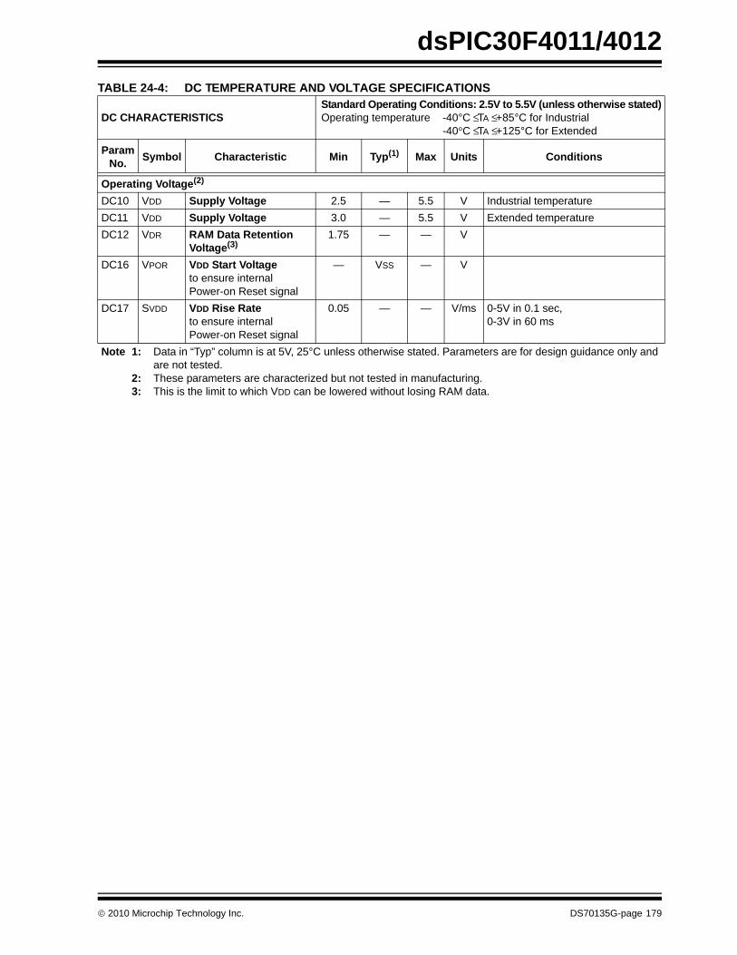
dsPIC30F4011/4012
TABLE 24-4: DC TEMPERATURE AND VOLTAGE SPECIFICATIONS
DC CHARACTERISTICSStandard Operating Conditions: 2.5V to 5.5V (unless otherwise stated)Operating temperature -40°C ≤ TA ≤ +85°C for Industrial
-40°C ≤ TA ≤ +125°C for Extended
Param No. Symbol Characteristic Min Typ(1) Max Units Conditions
Operating Voltage(2)
DC10 VDD Supply Voltage 2.5 — 5.5 V Industrial temperatureDC11 VDD Supply Voltage 3.0 — 5.5 V Extended temperatureDC12 VDR RAM Data Retention
Voltage(3)1.75 — — V
DC16 VPOR VDD Start Voltageto ensure internalPower-on Reset signal
— VSS — V
DC17 SVDD VDD Rise Rateto ensure internalPower-on Reset signal
0.05 — — V/ms 0-5V in 0.1 sec,0-3V in 60 ms
Note 1: Data in “Typ” column is at 5V, 25°C unless otherwise stated. Parameters are for design guidance only and are not tested.
2: These parameters are characterized but not tested in manufacturing.3: This is the limit to which VDD can be lowered without losing RAM data.
© 2010 Microchip Technology Inc. DS70135G-page 179

dsPIC30F4011/4012
TABLE 24-5: DC CHARACTERISTICS: OPERATING CURRENT (IDD)
DC CHARACTERISTICSStandard Operating Conditions: 2.5V to 5.5V (unless otherwise stated)Operating temperature -40°C ≤ TA ≤ +85°C for Industrial
-40°C ≤ TA ≤ +125°C for Extended
Parameter No. Typical(1) Max Units Conditions
Operating Current (IDD)(2)
DC31a 2 4 mA +25°C3.3V
0.128 MIPSLPRC (512 kHz)
DC31b 2 4 mA +85°CDC31c 2 4 mA +125°CDC31e 3 5 mA +25°C
5VDC31f 3 5 mA +85°CDC31g 3 5 mA +125°CDC30a 4 6 mA +25°C
3.3V
(1.8 MIPS)FRC (7.37 MHz)
DC30b 4 6 mA +85°CDC30c 4 6 mA +125°CDC30e 7 10 mA +25°C
5VDC30f 7 10 mA +85°CDC30g 7 10 mA +125°CDC23a 12 19 mA +25°C
3.3V
4 MIPS
DC23b 12 19 mA +85°CDC23c 13 19 mA +125°CDC23e 19 31 mA +25°C
5VDC23f 20 31 mA +85°CDC23g 20 31 mA +125°CDC24a 28 39 mA +25°C
3.3V
10 MIPS
DC24b 28 39 mA +85°CDC24c 29 39 mA +125°CDC24e 46 64 mA +25°C
5VDC24f 46 64 mA +85°CDC24g 47 64 mA +125°CDC27a 53 72 mA +25°C
3.3V
20 MIPSDC27b 53 72 mA +85°CDC27d 87 120 mA +25°C
5VDC27e 87 120 mA +85°CDC27f 87 120 mA +125°CDC29a 124 170 mA +25°C
5V 30 MIPSDC29b 125 170 mA +85°CNote 1: Data in “Typical” column is at 5V, 25°C unless otherwise stated. Parameters are for design guidance only
and are not tested.2: The supply current is mainly a function of the operating voltage and frequency. Other factors, such as I/O
pin loading and switching rate, oscillator type, internal code execution pattern and temperature, also have an impact on the current consumption. The test conditions for all IDD measurements are as follows: OSC1 driven with external square wave from rail to rail. All I/O pins are configured as inputs and pulled to VDD. MCLR = VDD, WDT, FSCM, LVD and BOR are disabled. CPU, SRAM, program memory and data memory are operational. No peripheral modules are operating.
DS70135G-page 180 © 2010 Microchip Technology Inc.

dsPIC30F4011/4012
TABLE 24-6: DC CHARACTERISTICS: IDLE CURRENT (IIDLE)
DC CHARACTERISTICSStandard Operating Conditions: 2.5V to 5.5V (unless otherwise stated)Operating temperature -40°C ≤ TA ≤ +85°C for Industrial
-40°C ≤ TA ≤ +125°C for Extended
Parameter No. Typical(1,2) Max Units Conditions
Operating Current (IDD)(3)
DC51a 1.3 3 mA +25°C3.3V
0.128 MIPSLPRC (512 kHz)
DC51b 1.3 3 mA +85°CDC51c 1.3 3 mA +125°CDC51e 2.7 5 mA +25°C
5VDC51f 2.7 5 mA +85°CDC51g 2.7 5 mA +125°CDC50a 4 6 mA +25°C
3.3V
(1.8 MIPS)FRC (7.37 MHz)
DC50b 4 6 mA +85°CDC50c 4 6 mA +125°CDC50e 7 11 mA +25°C
5VDC50f 7 11 mA +85°CDC50g 7 11 mA +125°CDC43a 7 11 mA +25°C
3.3V
4 MIPS
DC43b 7 11 mA +85°CDC43c 7 11 mA +125°CDC43e 12 17 mA +25°C
5VDC43f 12 17 mA +85°CDC43g 12 17 mA +125°CDC44a 15 22 mA +25°C
3.3V
10 MIPS
DC44b 15 22 mA +85°CDC44c 16 22 mA +125°CDC44e 26 36 mA +25°C
5VDC44f 27 36 mA +85°CDC44g 27 36 mA +125°CDC47a 30 40 mA +25°C
3.3V
20 MIPSDC47b 30 40 mA +85°CDC47d 50 65 mA +25°C
5VDC47e 50 65 mA +85°CDC47f 51 65 mA +125°CDC49a 72 95 mA +25°C
5V 30 MIPSDC49b 73 95 mA +85°CNote 1: Data in “Typical” column is at 5V, 25°C unless otherwise stated. Parameters are for design guidance only
and are not tested.2: Base IIDLE current is measured with core off, clock on and all modules turned off.
© 2010 Microchip Technology Inc. DS70135G-page 181

dsPIC30F4011/4012
TABLE 24-7: DC CHARACTERISTICS: POWER-DOWN CURRENT (IPD)
DC CHARACTERISTICSStandard Operating Conditions: 2.5V to 5.5V (unless otherwise stated)Operating temperature -40°C ≤ TA ≤ +85°C for Industrial
-40°C ≤ TA ≤ +125°C for Extended
Parameter No. Typical(1) Max Units Conditions
Power-Down Current (IPD)(2)
DC60a 0.3 — μA 25°C3.3V
Base power-down current(3)
DC60b 1 30 μA 85°CDC60c 12 60 μA 125°CDC60e 0.5 — μA 25°C
5VDC60f 2 45 μA 85°CDC60g 17 90 μA 125°CDC61a 5 8 μA 25°C
3.3V
Watchdog Timer current: ΔIWDT(3)
DC61b 5 8 μA 85°CDC61c 6 9 μA 125°CDC61e 10 15 μA 25°C
5VDC61f 10 15 μA 85°CDC61g 11 17 μA 125°CDC62a 4 10 μA 25°C
3.3V
Timer1 w/32 kHz crystal: ΔITI32(3)
DC62b 5 10 μA 85°CDC62c 4 10 μA 125°CDC62e 4 15 μA 25°C
5VDC62f 6 15 μA 85°CDC62g 5 15 μA 125°CDC63a 32 48 μA 25°C
3.3V
BOR on: ΔIBOR(3)
DC63b 35 53 μA 85°CDC63c 37 56 μA 125°CDC63e 37 56 μA 25°C
5VDC63f 41 62 μA 85°CDC63g 57 86 μA 125°CNote 1: Data in “Typ” column is at 5V, 25°C unless otherwise stated. Parameters are for design guidance only and
are not tested.2: These parameters are characterized but not tested in manufacturing.
DS70135G-page 182 © 2010 Microchip Technology Inc.
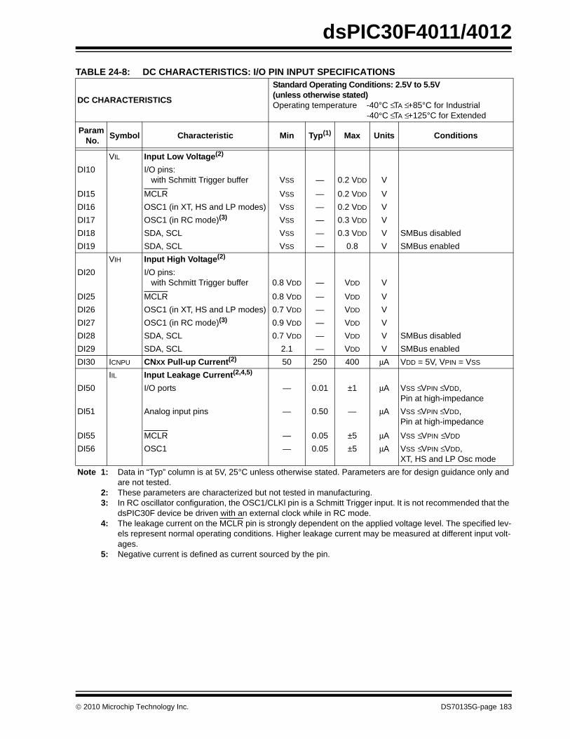
dsPIC30F4011/4012
TABLE 24-8: DC CHARACTERISTICS: I/O PIN INPUT SPECIFICATIONS
DC CHARACTERISTICS
Standard Operating Conditions: 2.5V to 5.5V (unless otherwise stated)Operating temperature -40°C ≤ TA ≤ +85°C for Industrial
-40°C ≤ TA ≤ +125°C for Extended
Param No. Symbol Characteristic Min Typ(1) Max Units Conditions
VIL Input Low Voltage(2)
DI10 I/O pins: with Schmitt Trigger buffer VSS — 0.2 VDD V
DI15 MCLR VSS — 0.2 VDD VDI16 OSC1 (in XT, HS and LP modes) VSS — 0.2 VDD VDI17 OSC1 (in RC mode)(3) VSS — 0.3 VDD VDI18 SDA, SCL VSS — 0.3 VDD V SMBus disabledDI19 SDA, SCL VSS — 0.8 V SMBus enabled
VIH Input High Voltage(2)
DI20 I/O pins: with Schmitt Trigger buffer 0.8 VDD — VDD V
DI25 MCLR 0.8 VDD — VDD VDI26 OSC1 (in XT, HS and LP modes) 0.7 VDD — VDD VDI27 OSC1 (in RC mode)(3) 0.9 VDD — VDD VDI28 SDA, SCL 0.7 VDD — VDD V SMBus disabledDI29 SDA, SCL 2.1 — VDD V SMBus enabledDI30 ICNPU CNXX Pull-up Current(2) 50 250 400 μA VDD = 5V, VPIN = VSS
IIL Input Leakage Current(2,4,5)
DI50 I/O ports — 0.01 ±1 μA VSS ≤ VPIN ≤ VDD,Pin at high-impedance
DI51 Analog input pins — 0.50 — μA VSS ≤ VPIN ≤ VDD,Pin at high-impedance
DI55 MCLR — 0.05 ±5 μA VSS ≤ VPIN ≤ VDD
DI56 OSC1 — 0.05 ±5 μA VSS ≤ VPIN ≤ VDD, XT, HS and LP Osc mode
Note 1: Data in “Typ” column is at 5V, 25°C unless otherwise stated. Parameters are for design guidance only and are not tested.
2: These parameters are characterized but not tested in manufacturing.3: In RC oscillator configuration, the OSC1/CLKl pin is a Schmitt Trigger input. It is not recommended that the
dsPIC30F device be driven with an external clock while in RC mode.4: The leakage current on the MCLR pin is strongly dependent on the applied voltage level. The specified lev-
els represent normal operating conditions. Higher leakage current may be measured at different input volt-ages.
5: Negative current is defined as current sourced by the pin.
© 2010 Microchip Technology Inc. DS70135G-page 183

dsPIC30F4011/4012
FIGURE 24-1: BROWN-OUT RESET CHARACTERISTICS
TABLE 24-9: DC CHARACTERISTICS: I/O PIN OUTPUT SPECIFICATIONS
DC CHARACTERISTICS
Standard Operating Conditions: 2.5V to 5.5V(unless otherwise stated)Operating temperature -40°C ≤ TA ≤ +85°C for Industrial
-40°C ≤ TA ≤ +125°C for Extended
Param No. Symbol Characteristic Min Typ(1) Max Units Conditions
VOL Output Low Voltage(2)
DO10 I/O ports — — 0.6 V IOL = 8.5 mA, VDD = 5V— — 0.15 V IOL = 2.0 mA, VDD = 3V
DO16 OSC2/CLKO — — 0.6 V IOL = 1.6 mA, VDD = 5V(RC or EC Osc mode) — — 0.72 V IOL = 2.0 mA, VDD = 3V
VOH Output High Voltage(2)
DO20 I/O ports VDD – 0.7 — — V IOH = -3.0 mA, VDD = 5VVDD – 0.2 — — V IOH = -2.0 mA, VDD = 3V
DO26 OSC2/CLKO VDD – 0.7 — — V IOH = -1.3 mA, VDD = 5V(RC or EC Osc mode) VDD – 0.1 — — V IOH = -2.0 mA, VDD = 3VCapacitive Loading Specs on Output Pins(2)
DO50 COSC2 OSC2/SOSC2 pin — — 15 pF In XTL, XT, HS and LP modes when external clock is used to drive OSC1
DO56 CIO All I/O pins and OSC2 — — 50 pF RC or EC Osc mode DO58 CB SCL, SDA — — 400 pF In I2C™ modeNote 1: Data in “Typ” column is at 5V, 25°C unless otherwise stated. Parameters are for design guidance only and
are not tested.2: These parameters are characterized but not tested in manufacturing.
BO10
Reset (due to BOR)
VDD
(Device in Brown-out Reset)
(Device not in Brown-out Reset)
Power-up Time-out
BO15
DS70135G-page 184 © 2010 Microchip Technology Inc.

dsPIC30F4011/4012
TABLE 24-10: ELECTRICAL CHARACTERISTICS: BOR
DC CHARACTERISTICSStandard Operating Conditions: 2.5V to 5.5V (unless otherwise stated)Operating temperature -40°C ≤ TA ≤ +85°C for Industrial
-40°C ≤ TA ≤ +125°C for Extended
ParamNo. Symbol Characteristic Min Typ(1) Max Units Conditions
BO10 VBOR BOR Voltage on VDD Transition High-to-Low(2)
BORV = 11(3) — — — V Not in operating rangeBORV = 10 2.6 — 2.71 VBORV = 01 4.1 — 4.4 VBORV = 00 4.58 — 4.73 V
BO15 VBHYS — 5 — mVNote 1: Data in “Typ” column is at 5V, 25°C unless otherwise stated. Parameters are for design guidance only and
are not tested.2: These parameters are characterized but not tested in manufacturing.3: ‘11’ values not in usable operating range.
TABLE 24-11: DC CHARACTERISTICS: PROGRAM AND EEPROM
DC CHARACTERISTICSStandard Operating Conditions: 2.5V to 5.5V (unless otherwise stated)Operating temperature -40°C ≤ TA ≤ +85°C for Industrial
-40°C ≤ TA ≤ +125°C for Extended
ParamNo. Symbol Characteristic Min Typ(1) Max Units Conditions
Data EEPROM Memory(2)
D120 ED Byte Endurance 100K 1M — E/W -40° C ≤ TA ≤ +85°CD121 VDRW VDD for Read/Write VMIN — 5.5 V Using EECON to read/write,
VMIN = Minimum operating voltageD122 TDEW Erase/Write Cycle Time 0.8 2 2.6 ms RTSPD123 TRETD Characteristic Retention 40 100 — Year Provided no other specifications are
violatedD124 IDEW IDD During Programming — 10 30 mA Row Erase
Program Flash Memory(2)
D130 EP Cell Endurance 10K 100K — E/W -40° C ≤ TA ≤ +85°CD131 VPR VDD for Read VMIN — 5.5 V VMIN = Minimum operating voltageD132 VEB VDD for Bulk Erase 4.5 — 5.5 VD133 VPEW VDD for Erase/Write 3.0 — 5.5 VD134 TPEW Erase/Write Cycle Time 0.8 2 2.6 ms RTSPD135 TRETD Characteristic Retention 40 100 — Year Provided no other specifications are
violatedD137 IPEW IDD During Programming — 10 30 mA Row EraseD138 IEB IDD During Programming — 10 30 mA Bulk EraseNote 1: Data in “Typ” column is at 5V, 25°C unless otherwise stated.
2: These parameters are characterized but not tested in manufacturing.
© 2010 Microchip Technology Inc. DS70135G-page 185

dsPIC30F4011/4012
24.2 AC Characteristics and Timing Parameters The information contained in this section defines dsPIC30F AC characteristics and timing parameters.TABLE 24-12: TEMPERATURE AND VOLTAGE SPECIFICATIONS – AC
FIGURE 24-2: LOAD CONDITIONS FOR DEVICE TIMING SPECIFICATIONS
FIGURE 24-3: EXTERNAL CLOCK TIMING
AC CHARACTERISTICS
Standard Operating Conditions: 2.5V to 5.5V(unless otherwise stated)Operating temperature -40°C ≤ TA ≤ +85°C for Industrial
-40°C ≤ TA ≤ +125°C for ExtendedOperating voltage VDD range as described in Section 24.1 “DC Characteristics”.
VDD/2
CL
RL
Pin
Pin
VSS
VSS
CL
RL = 464ΩCL = 50 pF for all pins except OSC2
5 pF for OSC2 output
Load Condition 1 – for all pins except OSC2 Load Condition 2 – for OSC2
OSC1
CLKO
Q4 Q1 Q2 Q3 Q4 Q1
OS20OS30 OS30
OS40 OS41
OS31 OS31OS25
DS70135G-page 186 © 2010 Microchip Technology Inc.

dsPIC30F4011/4012
TABLE 24-13: EXTERNAL CLOCK TIMING REQUIREMENTS
AC CHARACTERISTICS
Standard Operating Conditions: 2.5V to 5.5V(unless otherwise stated)Operating temperature -40°C ≤ TA ≤ +85°C for Industrial
-40°C ≤ TA ≤ +125°C for Extended
ParamNo. Symbol Characteristic Min Typ(1) Max Units Conditions
OS10 FOSC External CLKI Frequency(external clocks allowed onlyin EC mode)(2)
DC444
————
4010107.5
MHzMHzMHzMHz
ECEC with 4x PLLEC with 8x PLLEC with 16x PLL
Oscillator Frequency(2) DC0.44444
1031——
————————
7.37512
44
1010107.52533——
MHzMHzMHzMHzMHzMHzMHzkHzMHzkHz
RCXTLXTXT with 4x PLLXT with 8x PLLXT with 16x PLLHSLPFRC internalLPRC internal
OS20 TOSC TOSC = 1/FOSC — — — — See parameter OS10for FOSC value
OS25 TCY Instruction Cycle Time(2,3) 33 — DC ns See Table 24-16
OS30 TosL,TosH
External Clock in (OSC1)High or Low Time(2)
.45 x TOSC — — ns EC
OS31 TosR,TosF
External Clock in (OSC1)Rise or Fall Time(2)
— — 20 ns EC
OS40 TckR CLKO Rise Time(2,4) — — — ns See parameter DO31
OS41 TckF CLKO Fall Time(2,4) — — — ns See parameter DO32Note 1: Data in “Typ” column is at 5V, 25°C unless otherwise stated. Parameters are for design guidance only and
are not tested.2: These parameters are characterized but not tested in manufacturing.3: Instruction cycle period (TCY) equals four times the input oscillator time base period. All specified values
are based on characterization data for that particular oscillator type under standard operating conditions with the device executing code. Exceeding these specified limits may result in an unstable oscillator operation and/or higher than expected current consumption. All devices are tested to operate at “min.” values with an external clock applied to the OSC1/CLKI pin. When an external clock input is used, the “Max.” cycle time limit is “DC” (no clock) for all devices.
4: Measurements are taken in EC or ERC modes. The CLKO signal is measured on the OSC2 pin. CLKO is low for the Q1-Q2 period (1/2 TCY) and high for the Q3-Q4 period (1/2 TCY).
© 2010 Microchip Technology Inc. DS70135G-page 187

dsPIC30F4011/4012
TABLE 24-14: PLL CLOCK TIMING SPECIFICATIONS (VDD = 2.5 TO 5.5V)
AC CHARACTERISTICSStandard Operating Conditions: 2.5V to 5.5V (unless otherwise stated)Operating temperature -40°C ≤ TA ≤ +85°C for Industrial
-40°C ≤ TA ≤ +125°C for Extended
ParamNo. Symbol Characteristic(1) Min Typ(2) Max Units Conditions
OS50 FPLLI PLL Input Frequency Range(2) 444444
——————
1010
7.5(3)
1010
7.5(3)
MHzMHzMHzMHzMHzMHz
EC with 4x PLL EC with 8x PLL EC with 16x PLL XT with 4x PLLXT with 8x PLLXT with 16x PLL
OS51 FSYS On-Chip PLL Output(2) 16 — 120 MHz EC, XT with PLLOS52 TLOC PLL Start-up Time (Lock Time) — 20 50 μsNote 1: These parameters are characterized but not tested in manufacturing.
2: Data in “Typ” column is at 5V, 25°C unless otherwise stated. Parameters are for design guidance only and are not tested.
3: Limited by device operating frequency range.
TABLE 24-15: PLL JITTER
AC CHARACTERISTICS
Standard Operating Conditions: 2.5V to 5.5V(unless otherwise stated)Operating temperature -40°C ≤ TA ≤ +85°C for Industrial
-40°C ≤ TA ≤ +125°C for Extended
Param No. Characteristic Min Typ(1) Max Units Conditions
OS61 x4 PLL — 0.251 0.413 % -40°C ≤ TA ≤ +85°C VDD = 3.0 to 3.6V— 0.251 0.413 % -40°C ≤ TA ≤ +125°C VDD = 3.0 to 3.6V— 0.256 0.47 % -40°C ≤ TA ≤ +85°C VDD = 4.5 to 5.5V— 0.256 0.47 % -40°C ≤ TA ≤ +125°C VDD = 4.5 to 5.5V
x8 PLL — 0.355 0.584 % -40°C ≤ TA ≤ +85°C VDD = 3.0 to 3.6V— 0.355 0.584 % -40°C ≤ TA ≤ +125°C VDD = 3.0 to 3.6V— 0.362 0.664 % -40°C ≤ TA ≤ +85°C VDD = 4.5 to 5.5V— 0.362 0.664 % -40°C ≤ TA ≤ +125°C VDD = 4.5 to 5.5V
x16 PLL — 0.67 0.92 % -40°C ≤ TA ≤ +85°C VDD = 3.0 to 3.6V— 0.632 0.956 % -40°C ≤ TA ≤ +85°C VDD = 4.5 to 5.5V— 0.632 0.956 % -40°C ≤ TA ≤ +125°C VDD = 4.5 to 5.5V
Note 1: These parameters are characterized but not tested in manufacturing.
DS70135G-page 188 © 2010 Microchip Technology Inc.

dsPIC30F4011/4012
TABLE 24-16: INTERNAL CLOCK TIMING EXAMPLES Clock
OscillatorMode
FOSC (MHz)(1) TCY (μsec)(2) MIPS
w/o PLL(3)MIPS
w/PLL x4(3)MIPS
w/PLL x8(3)MIPS
w/PLL x16(3)
EC 0.200 20.0 0.05 — — —4 1.0 1.0 4.0 8.0 16.0
10 0.4 2.5 10.0 20.0 —25 0.16 6.25 — — —
XT 4 1.0 1.0 4.0 8.0 16.010 0.4 2.5 10.0 20.0 —
Note 1: Assumption: Oscillator postscaler is divide by 1.2: Instruction Execution Cycle Time: TCY = 1/MIPS.3: Instruction Execution Frequency: MIPS = (FOSC * PLLx)/4, since there are 4 Q clocks per instruction cycle.
© 2010 Microchip Technology Inc. DS70135G-page 189

dsPIC30F4011/4012
TABLE 24-17: AC CHARACTERISTICS: INTERNAL FRC ACCURACY
AC CHARACTERISTICSStandard Operating Conditions: 2.5V to 5.5V (unless otherwise stated)Operating temperature -40°C ≤ TA ≤ +85°C for Industrial
-40°C ≤ TA ≤ +125°C for Extended
Param No. Characteristic Min Typ Max Units Conditions
Internal FRC Accuracy @ FRC Freq. = 7.37 MHz(1)
OS63 FRC — — ±2.00 % -40°C ≤ TA ≤ +85°C VDD = 3.0-5.5V— — ±5.00 % -40°C ≤ TA ≤ +125°C VDD = 3.0-5.5V
Note 1: Frequency calibrated at 7.372 MHz ±2%, 25°C and 5V. TUN<3:0> bits can be used to compensate for temperature drift.
TABLE 24-18: AC CHARACTERISTICS: INTERNAL LPRC ACCURACY
AC CHARACTERISTICSStandard Operating Conditions: 2.5V to 5.5V (unless otherwise stated)Operating temperature -40°C ≤ TA ≤ +85°C for Industrial
-40°C ≤ TA ≤ +125°C for Extended
ParamNo. Characteristic Min Typ Max Units Conditions
LPRC @ Freq. = 512 kHz(1)
OS65A -50 — +50 % VDD = 5.0V, ±10%OS65B -60 — +60 % VDD = 3.3V, ±10%OS65C -70 — +70 % VDD = 2.5VNote 1: Change of LPRC frequency as VDD changes.
DS70135G-page 190 © 2010 Microchip Technology Inc.

dsPIC30F4011/4012
FIGURE 24-4: CLKO AND I/O TIMING CHARACTERISTICSNote: Refer to the Figure 24-2 for load.
I/O Pin(Input)
I/O Pin(Output)
DI35
Old Value New Value
DI40
DO31DO32
TABLE 24-19: CLKO AND I/O TIMING REQUIREMENTS
AC CHARACTERISTICSStandard Operating Conditions: 2.5V to 5.5V (unless otherwise stated)Operating temperature -40°C ≤ TA ≤ +85°C for Industrial
-40°C ≤ TA ≤ +125°C for Extended
ParamNo. Symbol Characteristic(1,2,3) Min Typ(4) Max Units Conditions
DO31 TIOR Port Output Rise Time — 7 20 nsDO32 TIOF Port Output Fall Time — 7 20 nsDI35 TINP INTx Pin High or Low Time (output) 20 — — nsDI40 TRBP CNx High or Low Time (input) 2 TCY — — nsNote 1: These parameters are asynchronous events not related to any internal clock edges
2: Measurements are taken in RC mode and EC mode where CLKO output is 4 x TOSC.3: These parameters are characterized but not tested in manufacturing.4: Data in “Typ” column is at 5V, 25°C unless otherwise stated.
© 2010 Microchip Technology Inc. DS70135G-page 191

dsPIC30F4011/4012
FIGURE 24-5: RESET, WATCHDOG TIMER, OSCILLATOR START-UP TIMER AND POWER-UPTIMER TIMING CHARACTERISTICS
VDD
MCLR
InternalPOR
PWRTTime-out
OscillatorTime-out
InternalReset
WatchdogTimerReset
SY11
SY10
SY20SY13
I/O Pins
SY13
Note: Refer to the Figure 24-2 for load conditions.
FSCM Delay
SY35
SY30
SY12
DS70135G-page 192 © 2010 Microchip Technology Inc.

dsPIC30F4011/4012
FIGURE 24-6: BAND GAP START-UP TIME CHARACTERISTICS
TABLE 24-20: RESET, WATCHDOG TIMER, OSCILLATOR START-UP TIMER, POWER-UP TIMER AND BROWN-OUT RESET TIMING REQUIREMENTS
AC CHARACTERISTICS
Standard Operating Conditions: 2.5V to 5.5V (unless otherwise stated)Operating temperature -40°C ≤ TA ≤ +85°C for Industrial
-40°C ≤ TA ≤ +125°C for Extended
ParamNo. Symbol Characteristic(1) Min Typ(2) Max Units Conditions
SY10 TmcL MCLR Pulse Width (low) 2 — — μs -40°C to +85°CSY11 TPWRT Power-up Timer Period 2
832
41664
62496
ms -40°C to +85°C, VDD = 5VUser programmable
SY12 TPOR Power-on Reset Delay 3 10 30 μs -40°C to +85°C
SY13 TIOZ I/O High-Impedance from MCLR Low or Watchdog Timer Reset
— 0.8 1.0 μs
SY20 TWDT1TWDT2TWDT3
Watchdog Timer Time-out Period (No Prescaler)
0.60.81.0
2.02.02.0
3.43.23.0
msmsms
VDD = 2.5VVDD = 3.3V, ±10%VDD = 5V, ±10%
SY25 TBOR Brown-out Reset Pulse Width(3) 100 — — μs VDD ≤ VBOR (D034)SY30 TOST Oscillation Start-up Timer Period — 1024 TOSC — — TOSC = OSC1 periodSY35 TFSCM Fail-Safe Clock Monitor Delay — 500 900 μs -40°C to +85°CNote 1: These parameters are characterized but not tested in manufacturing.
2: Data in “Typ” column is at 5V, 25°C unless otherwise stated.3: Refer to Figure 24-1 and Table 24-10 for BOR.
VBGAP
Enable
Band Gap
0V
Stable
Note 1: Band gap is enabled when FBORPOR<7> is set.
SY40
Band Gap(1)
TABLE 24-21: BAND GAP START-UP TIME REQUIREMENTS
AC CHARACTERISTICSStandard Operating Conditions: 2.5V to 5.5V (unless otherwise stated)Operating temperature -40°C ≤ TA ≤ +85°C for Industrial
-40°C ≤ TA ≤ +125°C for Extended
ParamNo. Symbol Characteristic(1) Min Typ(2) Max Units Conditions
SY40 TBGAP Band Gap Start-up Time
— 40 65 μs Defined as the time between the instant that the band gap is enabled and the moment that the band gap reference voltage is stable (RCON<13> status bit)
Note 1: These parameters are characterized but not tested in manufacturing.2: Data in “Typ” column is at 5V, 25°C unless otherwise stated.
© 2010 Microchip Technology Inc. DS70135G-page 193

dsPIC30F4011/4012
FIGURE 24-7: TIMERx EXTERNAL CLOCK TIMING CHARACTERISTICSNote: Refer to Figure 24-2 for load conditions.
Tx11
Tx15
Tx10
Tx20
TMRxOS60
TxCK
TABLE 24-22: TIMER1 EXTERNAL CLOCK TIMING REQUIREMENTS
AC CHARACTERISTICSStandard Operating Conditions: 2.5V to 5.5V (unless otherwise stated)Operating temperature -40°C ≤ TA ≤ +85°C for Industrial
-40°C ≤ TA ≤ +125°C for Extended
ParamNo. Symbol Characteristic Min Typ Max Units Conditions
TA10 TTXH T1CK High Time
Synchronous,no prescaler
0.5 TCY + 20 — — ns Must also meet parameter TA15
Synchronous,with prescaler
10 — — ns
Asynchronous 10 — — nsTA11 TTXL T1CK Low
TimeSynchronous,no prescaler
0.5 TCY + 20 — — ns Must also meet parameter TA15
Synchronous,with prescaler
10 — — ns
Asynchronous 10 — — nsTA15 TTXP T1CK Input
PeriodSynchronous,no prescaler
TCY + 10 — — ns
Synchronous,with prescaler
Greater of:20 ns or
(TCY + 40)/N
— — — N = prescale value(1, 8, 64, 256)
Asynchronous 20 — — nsOS60 Ft1 SOSCO/T1CK Oscillator
Input frequency Range (oscillator enabled by setting bit, TCS (T1CON<1>)
DC — 50 kHz
TA20 TCKEXTMRL Delay from External T1CK Clock Edge to Timer Increment
0.5 TCY — 1.5 TCY —
DS70135G-page 194 © 2010 Microchip Technology Inc.

dsPIC30F4011/4012
TABLE 24-23: TIMER2 AND TIMER4 EXTERNAL CLOCK TIMING REQUIREMENTS
AC CHARACTERISTICS
Standard Operating Conditions: 2.5V to 5.5V(unless otherwise stated)Operating temperature -40°C ≤ TA ≤ +85°C for Industrial
-40°C ≤ TA ≤ +125°C for Extended
ParamNo. Symbol Characteristic Min Typ Max Units Conditions
TB10 TTXH TxCK High Time Synchronous,no prescaler
0.5 TCY + 20 — — ns Must also meet parameter TB15
Synchronous,with prescaler
10 — — ns
TB11 TTXL TxCK Low Time Synchronous,no prescaler
0.5 TCY + 20 — — ns Must also meet parameter TB15
Synchronous,with prescaler
10 — — ns
TB15 TTXP TxCK Input Period
Synchronous,no prescaler
TCY + 10 — — ns N = prescale value(1, 8, 64, 256)Synchronous,
with prescalerGreater of:
20 ns or(TCY + 40)/N
TB20 TCKEXTMRL Delay from External TxCK Clock Edge to Timer Increment
0.5 TCY — 1.5 TCY —
TABLE 24-24: TIMER3 AND TIMER5 EXTERNAL CLOCK TIMING REQUIREMENTS
AC CHARACTERISTICS
Standard Operating Conditions: 2.5V to 5.5V(unless otherwise stated)Operating temperature -40°C ≤ TA ≤ +85°C for Industrial
-40°C ≤ TA ≤ +125°C for Extended
ParamNo. Symbol Characteristic Min Typ Max Units Conditions
TC10 TtxH TxCK High Time Synchronous 0.5 TCY + 20 — — ns Must also meet parameter TC15
TC11 TtxL TxCK Low Time Synchronous 0.5 TCY + 20 — — ns Must also meet parameter TC15
TC15 TtxP TxCK Input Period Synchronous,no prescaler
TCY + 10 — — ns N = prescalevalue (1, 8, 64, 256)Synchronous,
with prescalerGreater of:
20 ns or (TCY + 40)/N
TC20 TCKEXTMRL Delay from External TxCK Clock Edge to Timer Increment
0.5 TCY — 1.5 TCY —
© 2010 Microchip Technology Inc. DS70135G-page 195

dsPIC30F4011/4012
FIGURE 24-8: QEI MODULE EXTERNAL CLOCK TIMING CHARACTERISTICSTQ11
TQ15
TQ10
TQ20
QEB
POSCNT
TABLE 24-25: QEI MODULE EXTERNAL CLOCK TIMING REQUIREMENTS
AC CHARACTERISTICS
Standard Operating Conditions: 2.5V to 5.5V(unless otherwise stated)Operating temperature -40°C ≤ TA ≤ +85°C for Industrial
-40°C ≤ TA ≤ +125°C for Extended
ParamNo. Symbol Characteristic(1) Min Typ Max Units Conditions
TQ10 TtQH TxCK High Time Synchronous,with prescaler
TCY + 20 — — ns Must also meet parameter TQ15
TQ11 TtQL TxCK Low Time Synchronous,with prescaler
TCY + 20 — — ns Must also meet parameter TQ15
TQ15 TtQP TxCK Input Period Synchronous,with prescaler
2 * TCY + 40 — — ns
TQ20 TCKEXTMRL Delay from External TxCK Clock Edge to Timer Increment
0.5 TCY — 1.5 TCY ns
Note 1: These parameters are characterized but not tested in manufacturing.
DS70135G-page 196 © 2010 Microchip Technology Inc.

dsPIC30F4011/4012
FIGURE 24-9: INPUT CAPTURE TIMING CHARACTERISTICSICX
IC10 IC11
IC15
Note: Refer to Figure 24-2 for load conditions.
TABLE 24-26: INPUT CAPTURE TIMING REQUIREMENTS
AC CHARACTERISTICSStandard Operating Conditions: 2.5V to 5.5V (unless otherwise stated)Operating temperature -40°C ≤ TA ≤ +85°C for Industrial
-40°C ≤ TA ≤ +125°C for Extended
ParamNo. Symbol Characteristic(1) Min Max Units Conditions
IC10 TccL ICx Input Low Time No prescaler 0.5 TCY + 20 — nsWith prescaler 10 — ns
IC11 TccH ICx Input High Time No prescaler 0.5 TCY + 20 — nsWith prescaler 10 — ns
IC15 TccP ICx Input Period (2 TCY + 40)/N — ns N = prescale value (1, 4, 16)
Note 1: These parameters are characterized but not tested in manufacturing.
© 2010 Microchip Technology Inc. DS70135G-page 197

dsPIC30F4011/4012
FIGURE 24-10: OUTPUT COMPARE MODULE TIMING CHARACTERISTICSOCx
OC11 OC10(Output Compare
Note: Refer to Figure 24-2 for load conditions.
or PWM Mode)
TABLE 24-27: OUTPUT COMPARE MODULE TIMING REQUIREMENTS
AC CHARACTERISTICS
Standard Operating Conditions: 2.5V to 5.5V (unless otherwise stated)Operating temperature -40°C ≤ TA ≤ +85°C for Industrial
-40°C ≤ TA ≤ +125°C for Extended
Param No. Symbol Characteristic(1) Min Typ(2) Max Units Conditions
OC10 TccF OCx Output Fall Time — — — ns See parameter DO32OC11 TccR OCx Output Rise Time — — — ns See parameter DO31Note 1: These parameters are characterized but not tested in manufacturing.
2: Data in “Typ” column is at 5V, 25°C unless otherwise stated. Parameters are for design guidance only and are not tested.
DS70135G-page 198 © 2010 Microchip Technology Inc.

dsPIC30F4011/4012
FIGURE 24-11: OUTPUT COMPARE/PWM MODULE TIMING CHARACTERISTICSOCFA
OCx
OC20
OC15
TABLE 24-28: SIMPLE OUTPUT COMPARE/PWM MODE TIMING REQUIREMENTS
AC CHARACTERISTICS
Standard Operating Conditions: 2.5V to 5.5V(unless otherwise stated)Operating temperature -40°C ≤ TA ≤ +85°C for Industrial
-40°C ≤ TA ≤ +125°C for Extended
Param No. Symbol Characteristic(1) Min Typ(2) Max Units Conditions
OC15 TFD Fault Input to PWM I/O Change
— — 50 ns
OC20 TFLT Fault Input Pulse Width 50 — — nsNote 1: These parameters are characterized but not tested in manufacturing.
2: Data in “Typ” column is at 5V, 25°C unless otherwise stated. Parameters are for design guidance only and are not tested.
© 2010 Microchip Technology Inc. DS70135G-page 199

dsPIC30F4011/4012
FIGURE 24-12: MOTOR CONTROL PWM MODULE FAULT TIMING CHARACTERISTICSFIGURE 24-13: MOTOR CONTROL PWM MODULE TIMING CHARACTERISTICS
FLTA
PWMx
MP30
MP20
PWMx
MP11 MP10
Note: Refer to Figure 24-2 for load conditions.
TABLE 24-29: MOTOR CONTROL PWM MODULE TIMING REQUIREMENTS
AC CHARACTERISTICS
Standard Operating Conditions: 2.5V to 5.5V(unless otherwise stated)Operating temperature -40°C ≤ TA ≤ +85°C for Industrial
-40°C ≤ TA ≤ +125°C for Extended
ParamNo. Symbol Characteristic(1) Min Typ(2) Max Units Conditions
MP10 TFPWM PWM Output Fall Time — — — ns See parameter DO32MP11 TRPWM PWM Output Rise
Time— — — ns See parameter DO31
MP20 TFD Fault Input ↓ to PWMI/O Change
— — 50 ns
MP30 TFH Minimum Pulse Width 50 — — nsNote 1: These parameters are characterized but not tested in manufacturing.
2: Data in “Typ” column is at 5V, 25°C unless otherwise stated. Parameters are for design guidance only and are not tested.
DS70135G-page 200 © 2010 Microchip Technology Inc.

dsPIC30F4011/4012
FIGURE 24-14: QEA/QEB INPUT CHARACTERISTICSTQ30
TQ35
TQ31
QEA(input)
TQ35
QEB(input)
TQ36
QEBInternal
TQ40TQ41
TQ30TQ31
TABLE 24-30: QUADRATURE DECODER TIMING REQUIREMENTS
AC CHARACTERISTICS
Standard Operating Conditions: 2.5V to 5.5V(unless otherwise stated)Operating temperature -40°C ≤ TA ≤ +85°C for Industrial
-40°C ≤ TA ≤ +125°C for Extended
ParamNo. Symbol Characteristic(1) Typ(2) Max Units Conditions
TQ30 TQUL Quadrature Input Low Time 6 TCY — nsTQ31 TQUH Quadrature Input High Time 6 TCY — nsTQ35 TQUIN Quadrature Input Period 12 TCY — nsTQ36 TQUP Quadrature Phase Period 3 TCY — nsTQ40 TQUFL Filter Time to Recognize Low,
with Digital Filter3 * N * TCY — ns N = 1, 2, 4, 16, 32, 64, 128
and 256 (Note 2)TQ41 TQUFH Filter Time to Recognize High,
with Digital Filter3 * N * TCY — ns N = 1, 2, 4, 16, 32, 64, 128
and 256 (Note 2)Note 1: These parameters are characterized but not tested in manufacturing.
2: N = Index Channel Digital Filter Clock Divide Select bits. Refer to Section 16. “Quadrature Encoder Interface (QEI)” in the “dsPIC30F Family Reference Manual” (DS70046).
© 2010 Microchip Technology Inc. DS70135G-page 201

dsPIC30F4011/4012
FIGURE 24-15: QEI MODULE INDEX PULSE TIMING CHARACTERISTICSQEA(input)
UngatedIndex
QEB(input)
TQ55
Index Internal
Position CounterReset
TQ50TQ51
TABLE 24-31: QEI INDEX PULSE TIMING REQUIREMENTS
AC CHARACTERISTICS
Standard Operating Conditions: 2.5V to 5.5V(unless otherwise stated)Operating temperature -40°C ≤ TA ≤ +85°C for Industrial
-40°C ≤ TA ≤ +125°C for Extended
ParamNo. Symbol Characteristic(1) Min Max Units Conditions
TQ50 TqIL Filter Time to Recognize Low,with Digital Filter
3 * N * TCY — ns N = 1, 2, 4, 16, 32, 64,128 and 256 (Note 2)
TQ51 TqiH Filter Time to Recognize High,with Digital Filter
3 * N * TCY — ns N = 1, 2, 4, 16, 32, 64,128 and 256 (Note 2)
TQ55 Tqidxr Index Pulse Recognized to PositionCounter Reset (ungated index)
3 TCY — ns
Note 1: These parameters are characterized but not tested in manufacturing.2: Alignment of index pulses to QEA and QEB is shown for position counter Reset timing only. Shown for
forward direction only (QEA leads QEB). Same timing applies for reverse direction (QEA lags QEB) but index pulse recognition occurs on falling edge.
DS70135G-page 202 © 2010 Microchip Technology Inc.

dsPIC30F4011/4012
© 2010 Microchip Technology Inc. DS70135G-page 203
FIGURE 24-16: SPI MODULE MASTER MODE (CKE = 0) TIMING CHARACTERISTICS
SCK1(CKP = 0)
SCK1(CKP = 1)
SDO1
SDI1
SP11 SP10
SP40 SP41
SP21SP20SP35
SP20SP21
MSb LSbBit 14 - - - - - -1
LSb InBit 14 - - - -1
SP30SP31
Note: Refer to Figure 24-2 for load conditions.
MSb In
TABLE 24-32: SPI MASTER MODE (CKE = 0) TIMING REQUIREMENTS
AC CHARACTERISTICS
Standard Operating Conditions: 2.5V to 5.5V(unless otherwise stated)Operating temperature -40°C ≤ TA ≤ +85°C for Industrial
-40°C ≤ TA ≤ +125°C for Extended
ParamNo. Symbol Characteristic(1) Min Typ(2) Max Units Conditions
SP10 TscL SCK1 Output Low Time(3) TCY/2 — — nsSP11 TscH SCK1 Output High Time(3) TCY/2 — — nsSP20 TscF SCK1 Output Fall Time(4 — — — ns See parameter DO32SP21 TscR SCK1 Output Rise Time(4) — — — ns See parameter DO31SP30 TdoF SDO1 Data Output Fall Time(4) — — — ns See parameter DO32SP31 TdoR SDO1 Data Output Rise
Time(4)— — — ns See parameter DO31
SP35 TscH2doV,TscL2doV
SDO1 Data Output Valid after SCK1 Edge
— — 30 ns
SP40 TdiV2scH,TdiV2scL
Setup Time of SDI1 Data Inputto SCK1 Edge
20 — — ns
SP41 TscH2diL,TscL2diL
Hold Time of SDI1 Data Inputto SCK1 Edge
20 — — ns
Note 1: These parameters are characterized but not tested in manufacturing.2: Data in “Typ” column is at 5V, 25°C unless otherwise stated. Parameters are for design guidance only and
are not tested.3: The minimum clock period for SCK1 is 100 ns. Therefore, the clock generated in Master mode must not
violate this specification.4: Assumes 50 pF load on all SPI pins.

dsPIC30F4011/4012
FIGURE 24-17: SPI MODULE MASTER MODE (CKE =1) TIMING CHARACTERISTICSSCK1(CKP = 0)
SCK1(CKP = 1)
SDO1
SDI1
SP36
SP30,SP31
SP35
MSb Bit 14 - - - - - -1
LSb InBit 14 - - - -1
LSb
Note: Refer to Figure 24-2 for load conditions.
SP11 SP10
SP21SP20
SP41
SP20SP21
MSb In
SP40
TABLE 24-33: SPI MODULE MASTER MODE (CKE = 1) TIMING REQUIREMENTS
AC CHARACTERISTICS
Standard Operating Conditions: 2.5V to 5.5V(unless otherwise stated)Operating temperature -40°C ≤ TA ≤ +85°C for Industrial
-40°C ≤ TA ≤ +125°C for Extended
ParamNo. Symbol Characteristic(1) Min Typ(2) Max Units Conditions
SP10 TscL SCK1 Output Low Time(3) TCY/2 — — nsSP11 TscH SCK1 Output High Time(3) TCY/2 — — nsSP20 TscF SCK1 Output Fall Time(4) — — — ns See parameter DO32SP21 TscR SCK1 Output Rise Time(4) — — — ns See parameter DO31SP30 TdoF SDO1 Data Output Fall
Time(4)— — — ns See parameter DO32
SP31 TdoR SDO1 Data Output Rise Time(4)
— — — ns See parameter DO31
SP35 TscH2doV,TscL2doV
SDO1 Data Output Valid afterSCK1 Edge
— — 30 ns
SP36 TdoV2sc, TdoV2scL
SDO1 Data Output Setup toFirst SCK1 Edge
30 — — ns
SP40 TdiV2scH, TdiV2scL
Setup Time of SDI1 Data Input to SCK1 Edge
20 — — ns
SP41 TscH2diL, TscL2diL
Hold Time of SDI1 Data Inputto SCK1 Edge
20 — — ns
Note 1: These parameters are characterized but not tested in manufacturing.2: Data in “Typ” column is at 5V, 25°C unless otherwise stated. Parameters are for design guidance only and
are not tested.3: The minimum clock period for SCK1 is 100 ns. Therefore, the clock generated in Master mode must not
violate this specification.4: Assumes 50 pF load on all SPI pins.
DS70135G-page 204 © 2010 Microchip Technology Inc.

dsPIC30F4011/4012
FIGURE 24-18: SPI MODULE SLAVE MODE (CKE = 0) TIMING CHARACTERISTICSSS1
SCK1(CKP = 0)
SCK1(CKP = 1)
SDO1
SDI
SP50
SP40
SP41
SP30,SP31 SP51
SP35
SDI1
MSb LSbBit 14 - - - - - -1
Bit 14 - - - -1 LSb In
SP52
SP73SP72
SP72SP73SP71 SP70
Note: Refer to Figure 24-2 for load conditions.
MSb In
© 2010 Microchip Technology Inc. DS70135G-page 205
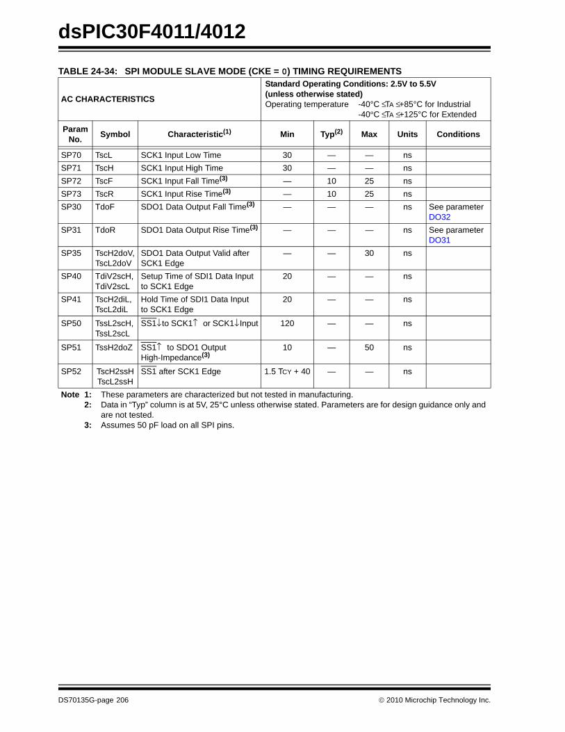
dsPIC30F4011/4012
TABLE 24-34: SPI MODULE SLAVE MODE (CKE = 0) TIMING REQUIREMENTS
AC CHARACTERISTICS
Standard Operating Conditions: 2.5V to 5.5V(unless otherwise stated)Operating temperature -40°C ≤ TA ≤ +85°C for Industrial
-40°C ≤ TA ≤ +125°C for Extended
ParamNo. Symbol Characteristic(1) Min Typ(2) Max Units Conditions
SP70 TscL SCK1 Input Low Time 30 — — nsSP71 TscH SCK1 Input High Time 30 — — nsSP72 TscF SCK1 Input Fall Time(3) — 10 25 nsSP73 TscR SCK1 Input Rise Time(3) — 10 25 nsSP30 TdoF SDO1 Data Output Fall Time(3) — — — ns See parameter
DO32SP31 TdoR SDO1 Data Output Rise Time(3) — — — ns See parameter
DO31SP35 TscH2doV,
TscL2doVSDO1 Data Output Valid afterSCK1 Edge
— — 30 ns
SP40 TdiV2scH, TdiV2scL
Setup Time of SDI1 Data Inputto SCK1 Edge
20 — — ns
SP41 TscH2diL, TscL2diL
Hold Time of SDI1 Data Inputto SCK1 Edge
20 — — ns
SP50 TssL2scH, TssL2scL
SS1↓ to SCK1↑ or SCK1↓ Input 120 — — ns
SP51 TssH2doZ SS1↑ to SDO1 OutputHigh-Impedance(3)
10 — 50 ns
SP52 TscH2ssHTscL2ssH
SS1 after SCK1 Edge 1.5 TCY + 40 — — ns
Note 1: These parameters are characterized but not tested in manufacturing.2: Data in “Typ” column is at 5V, 25°C unless otherwise stated. Parameters are for design guidance only and
are not tested.3: Assumes 50 pF load on all SPI pins.
DS70135G-page 206 © 2010 Microchip Technology Inc.

dsPIC30F4011/4012
FIGURE 24-19: SPI MODULE SLAVE MODE (CKE = 1) TIMING CHARACTERISTICSSS1
SCK1(CKP = 0)
SCK1(CKP = 1)
SDO1
SDI
SP60
SDI1
SP30,SP31
MSb Bit 14 - - - - - -1 LSb
SP51
Bit 14 - - - -1 LSb In
SP35
SP52
SP52
SP73SP72
SP72SP73SP71 SP70
SP40
SP41
Note: Refer to Figure 24-2 for load conditions.
SP50
MSb In
© 2010 Microchip Technology Inc. DS70135G-page 207

dsPIC30F4011/4012
TABLE 24-35: SPI MODULE SLAVE MODE (CKE = 1) TIMING REQUIREMENTS
AC CHARACTERISTICS
Standard Operating Conditions: 2.5V to 5.5V(unless otherwise stated)Operating temperature -40°C ≤ TA ≤ +85°C for Industrial
-40°C ≤ TA ≤ +125°C for Extended
ParamNo. Symbol Characteristic(1) Min Typ(2) Max Units Conditions
SP70 TscL SCK1 Input Low Time 30 — — nsSP71 TscH SCK1 Input High Time 30 — — nsSP72 TscF SCK1 Input Fall Time(3) — 10 25 nsSP73 TscR SCK1 Input Rise Time(3) — 10 25 nsSP30 TdoF SDO1 Data Output Fall Time(3) — — — ns See parameter DO32SP31 TdoR SDO1 Data Output Rise Time(3) — — — ns See parameter DO31SP35 TscH2doV,
TscL2doVSDO1 Data Output Valid afterSCK1 Edge
— — 30 ns
SP40 TdiV2scH, TdiV2scL
Setup Time of SDI1 Data Inputto SCK1 Edge
20 — — ns
SP41 TscH2diL, TscL2diL
Hold Time of SDI1 Data Inputto SCK1 Edge
20 — — ns
SP50 TssL2scH, TssL2scL
SS1↓ to SCK1↓ or SCK1↑ Input 120 — — ns
SP51 TssH2doZ SS1↑ to SDO1 OutputHigh-Impedance(4)
10 — 50 ns
SP52 TscH2ssHTscL2ssH
SS1↑ after SCK1 Edge 1.5 TCY + 40 — — ns
SP60 TssL2doV SDO1 Data Output Valid afterSS1 Edge
— — 50 ns
Note 1: These parameters are characterized but not tested in manufacturing.2: Data in “Typ” column is at 5V, 25°C unless otherwise stated. Parameters are for design guidance only and
are not tested.3: The minimum clock period for SCK1 is 100 ns. Therefore, the clock generated in Master mode must not
violate this specification.4: Assumes 50 pF load on all SPI pins.
DS70135G-page 208 © 2010 Microchip Technology Inc.

dsPIC30F4011/4012
FIGURE 24-20: I2C™ BUS START/STOP BITS TIMING CHARACTERISTICS (MASTER MODE)FIGURE 24-21: I2C™ BUS DATA TIMING CHARACTERISTICS (MASTER MODE)
IM34SCL
SDA
StartCondition
StopCondition
IM33
Note: Refer to Figure 24-2 for load conditions.
IM31
IM30
IM11IM10 IM33
IM11IM10
IM20
IM26IM25
IM40 IM40 IM45
IM21
SCL
SDAIn
SDAOut
Note: Refer to Figure 24-2 for load conditions.
© 2010 Microchip Technology Inc. DS70135G-page 209

dsPIC30F4011/4012
DS70135G-page 210 © 2010 Microchip Technology Inc.
I
TABLE 24-36: I2C™ BUS DATA TIMING REQUIREMENTS (MASTER MODE)
AC CHARACTERISTICS
Standard Operating Conditions: 2.5V to 5.5V(unless otherwise stated)Operating temperature -40°C ≤ TA ≤ +85°C for Industrial
-40°C ≤ TA ≤ +125°C for Extended
ParamNo. Symbol Characteristic Min(1) Max Units Conditions
IM10 TLO:SCL Clock Low Time 100 kHz mode TCY/2 (BRG + 1) — μs400 kHz mode TCY/2 (BRG + 1) — μs1 MHz mode(2) TCY/2 (BRG + 1) — μs
IM11 THI:SCL Clock High Time 100 kHz mode TCY/2 (BRG + 1) — μs400 kHz mode TCY/2 (BRG + 1) — μs1 MHz mode(2) TCY/2 (BRG + 1) — μs
IM20 TF:SCL SDA and SCLFall Time
100 kHz mode — 300 ns CB is specified to be from 10 to 400 pF400 kHz mode 20 + 0.1 CB 300 ns
1 MHz mode(2) — 100 nsIM21 TR:SCL SDA and SCL
Rise Time100 kHz mode — 1000 ns CB is specified to be
from 10 to 400 pF400 kHz mode 20 + 0.1 CB 300 ns1 MHz mode(2) — 300 ns
IM25 TSU:DAT Data InputSetup Time
100 kHz mode 250 — ns400 kHz mode 100 — ns1 MHz mode(2) — — ns
IM26 THD:DAT Data InputHold Time
100 kHz mode 0 — ns400 kHz mode 0 0.9 μs1 MHz mode(2) — — ns
IM30 TSU:STA Start ConditionSetup Time
100 kHz mode TCY/2 (BRG + 1) — μs Only relevant for Repeated Startcondition
400 kHz mode TCY/2 (BRG + 1) — μs1 MHz mode(2) TCY/2 (BRG + 1) — μs
IM31 THD:STA Start Condition Hold Time
100 kHz mode TCY/2 (BRG + 1) — μs After this period, thefirst clock pulse isgenerated
400 kHz mode TCY/2 (BRG + 1) — μs1 MHz mode(2) TCY/2 (BRG + 1) — μs
IM33 TSU:STO Stop Condition Setup Time
100 kHz mode TCY/2 (BRG + 1) — μs400 kHz mode TCY/2 (BRG + 1) — μs1 MHz mode(2) TCY/2 (BRG + 1) — μs
IM34 THD:STO Stop Condition 100 kHz mode TCY/2 (BRG + 1) — nsHold Time 400 kHz mode TCY/2 (BRG + 1) — ns
1 MHz mode(2) TCY/2 (BRG + 1) — nsIM40 TAA:SCL Output Valid
From Clock100 kHz mode — 3500 ns400 kHz mode — 1000 ns1 MHz mode(2) — — ns
IM45 TBF:SDA Bus Free Time 100 kHz mode 4.7 — μs Time the bus must be free before a newtransmission can start
400 kHz mode 1.3 — μs1 MHz mode(2) — — μs
IM50 CB Bus Capacitive Loading — 400 pF Note 1: BRG is the value of the I2C Baud Rate Generator. Refer to Section 21. “Inter-Integrated Circuit (I2C™)”
in the “dsPIC30F Family Reference Manual” (DS70046).2: Maximum pin capacitance = 10 pF for all I2C pins (for 1 MHz mode only).

dsPIC30F4011/4012
FIGURE 24-22: I2C™ BUS START/STOP BITS TIMING CHARACTERISTICS (SLAVE MODE)FIGURE 24-23: I2C™ BUS DATA TIMING CHARACTERISTICS (SLAVE MODE)
SCL
SDA
StartCondition
StopCondition
IS31
IS30
IS34
IS33
IS30IS31 IS33
IS11
IS10
IS20
IS26IS25
IS40 IS40 IS45
IS21
SCL
SDAIn
SDAOut
© 2010 Microchip Technology Inc. DS70135G-page 211

dsPIC30F4011/4012
TABLE 24-37: I2C™ BUS DATA TIMING REQUIREMENTS (SLAVE MODE)
AC CHARACTERISTICSStandard Operating Conditions: 2.5V to 5.5V (unless otherwise stated)Operating temperature -40°C ≤ TA ≤ +85°C for Industrial
-40°C ≤ TA ≤ +125°C for Extended
ParamNo. Symbol Characteristic Min Max Units Conditions
IS10 TLO:SCL Clock Low Time 100 kHz mode 4.7 — μs Device must operate at a minimum of 1.5 MHz
400 kHz mode 1.3 — μs Device must operate at a minimum of 10 MHz.
1 MHz mode(1) 0.5 — μsIS11 THI:SCL Clock High Time 100 kHz mode 4.0 — μs Device must operate at a
minimum of 1.5 MHz400 kHz mode 0.6 — μs Device must operate at a
minimum of 10 MHz1 MHz mode(1) 0.5 — μs
IS20 TF:SCL SDA and SCLFall Time
100 kHz mode — 300 ns CB is specified to be from10 to 400 pF400 kHz mode 20 + 0.1 CB 300 ns
1 MHz mode(1) — 100 nsIS21 TR:SCL SDA and SCL
Rise Time100 kHz mode — 1000 ns CB is specified to be from
10 to 400 pF400 kHz mode 20 + 0.1 CB 300 ns1 MHz mode(1) — 300 ns
IS25 TSU:DAT Data InputSetup Time
100 kHz mode 250 — ns400 kHz mode 100 — ns1 MHz mode(1) 100 — ns
IS26 THD:DAT Data InputHold Time
100 kHz mode 0 — ns400 kHz mode 0 0.9 μs1 MHz mode(1) 0 0.3 μs
IS30 TSU:STA Start ConditionSetup Time
100 kHz mode 4.7 — μs Only relevant for Repeated Start condition400 kHz mode 0.6 — μs
1 MHz mode(1) 0.25 — μsIS31 THD:STA Start Condition
Hold Time 100 kHz mode 4.0 — μs After this period, the first
clock pulse is generated400 kHz mode 0.6 — μs1 MHz mode(1) 0.25 — μs
IS33 TSU:STO Stop Condition Setup Time
100 kHz mode 4.7 — μs400 kHz mode 0.6 — μs1 MHz mode(1) 0.6 — μs
IS34 THD:STO Stop Condition 100 kHz mode 4000 — nsHold Time 400 kHz mode 600 — ns
1 MHz mode(1) 250 nsIS40 TAA:SCL Output Valid
From Clock100 kHz mode 0 3500 ns400 kHz mode 0 1000 ns1 MHz mode(1) 0 350 ns
IS45 TBF:SDA Bus Free Time 100 kHz mode 4.7 — μs Time the bus must be free before a new transmission can start
400 kHz mode 1.3 — μs1 MHz mode(1) 0.5 — μs
IS50 CB Bus Capacitive Loading — 400 pF Note 1: Maximum pin capacitance = 10 pF for all I2C pins (for 1 MHz mode only).
DS70135G-page 212 © 2010 Microchip Technology Inc.

dsPIC30F4011/4012
FIGURE 24-24: CAN MODULE I/O TIMING CHARACTERISTICSC1TX Pin(output)
CA10 CA11
Old Value New Value
CA20
C1RX Pin(input)
TABLE 24-38: CAN MODULE I/O TIMING REQUIREMENTS
AC CHARACTERISTICS
Standard Operating Conditions: 2.5V to 5.5V(unless otherwise stated)Operating temperature -40°C ≤ TA ≤ +85°C for Industrial
-40°C ≤ TA ≤ +125°C for Extended
ParamNo. Symbol Characteristic(1) Min Typ(2) Max Units Conditions
CA10 TioF Port Output Fall Time — — — ns See parameter DO32CA11 TioR Port Output Rise Time — — — ns See parameter DO31CA20 Tcwf Pulse Width to Trigger
CAN Wake-up Filter500 — — ns
Note 1: These parameters are characterized but not tested in manufacturing.2: Data in “Typ” column is at 5V, 25°C unless otherwise stated. Parameters are for design guidance only and
are not tested.
© 2010 Microchip Technology Inc. DS70135G-page 213

dsPIC30F4011/4012
TABLE 24-39: 10-BIT HIGH-SPEED A/D MODULE SPECIFICATIONS
AC CHARACTERISTICS
Standard Operating Conditions: 2.5V to 5.5V(unless otherwise stated)Operating temperature -40°C ≤ TA ≤ +85°C for Industrial
-40°C ≤ TA ≤ +125°C for Extended
Param No. Symbol Characteristic Min. Typ Max. Units Conditions
Device SupplyAD01 AVDD Module VDD Supply Greater of
VDD – 0.3or 2.7
— Lesser ofVDD + 0.3
or 5.5
V
AD02 AVSS Module VSS Supply VSS – 0.3 — VSS + 0.3 VReference Inputs AD05 VREFH Reference Voltage High AVSS + 2.7 — AVDD VAD06 VREFL Reference Voltage Low AVSS — AVDD – 2.7 VAD07 VREF Absolute Reference Voltage AVSS – 0.3 — AVDD + 0.3 VAD08 IREF Current Drain — 200
.0013003
μAμA
A/D operatingA/D off
Analog InputAD10 VINH-VINL Full-Scale Input Span VREFL — VREFH VAD11 VIN Absolute Input Voltage AVSS – 0.3 — AVDD + 0.3 VAD12 — Leakage Current — ±0.001 ±0.244 μA VINL = AVSS = VREFL = 0V,
AVDD = VREFH = 5V,Source Impedance = 5 kΩ
AD13 — Leakage Current — ±0.001 ±0.244 μA VINL = AVSS = VREFL = 0V,AVDD = VREFH = 3V,Source Impedance = 5 kΩ
AD17 RIN Recommended Impedanceof Analog Voltage Source
— — 5K Ω
DC AccuracyAD20 Nr Resolution 10 data bits bitsAD21 INL Integral Nonlinearity(3) — ±1 ±1 LSb VINL = AVSS = VREFL = 0V,
AVDD = VREFH = 5VAD21A INL Integral Nonlinearity(3) — ±1 ±1 LSb VINL = AVSS = VREFL = 0V,
AVDD = VREFH = 3VAD22 DNL Differential Nonlinearity(3) — ±1 ±1 LSb VINL = AVSS = VREFL = 0V,
AVDD = VREFH = 5VAD22A DNL Differential Nonlinearity(3) — ±1 ±1 LSb VINL = AVSS = VREFL = 0V,
AVDD = VREFH = 3VAD23 GERR Gain Error(3) ±1 ±5 ±6 LSb VINL = AVSS = VREFL = 0V,
AVDD = VREFH = 5VAD23A GERR Gain Error(3) ±1 ±5 ±6 LSb VINL = AVSS = VREFL = 0V,
AVDD = VREFH = 3VAD24 EOFF Offset Error ±1 ±2 ±3 LSb VINL = AVSS = VREFL = 0V,
AVDD = VREFH = 5VAD24A EOFF Offset Error ±1 ±2 ±3 LSb VINL = AVSS = VREFL = 0V,
AVDD = VREFH = 3VAD25 — Monotonicity(2) — — — — GuaranteedNote 1: Because the sample caps will eventually lose charge, clock rates below 10 kHz can affect linearity
performance, especially at elevated temperatures.2: The A/D conversion result never decreases with an increase in the input voltage and has no missing codes.3: Measurements taken with external VREF+ and VREF- used as the ADC voltage references.
DS70135G-page 214 © 2010 Microchip Technology Inc.

dsPIC30F4011/4012
Dynamic PerformanceAD30 THD Total Harmonic Distortion — -64 -67 dBAD31 SINAD Signal to Noise and
Distortion — 57 58 dB
AD32 SFDR Spurious Free Dynamic Range
— 67 71 dB
AD33 FNYQ Input Signal Bandwidth — — 500 kHzAD34 ENOB Effective Number of Bits 9.29 9.41 — bits
TABLE 24-39: 10-BIT HIGH-SPEED A/D MODULE SPECIFICATIONS (CONTINUED)
AC CHARACTERISTICS
Standard Operating Conditions: 2.5V to 5.5V(unless otherwise stated)Operating temperature -40°C ≤ TA ≤ +85°C for Industrial
-40°C ≤ TA ≤ +125°C for Extended
Param No. Symbol Characteristic Min. Typ Max. Units Conditions
Note 1: Because the sample caps will eventually lose charge, clock rates below 10 kHz can affect linearity performance, especially at elevated temperatures.
2: The A/D conversion result never decreases with an increase in the input voltage and has no missing codes.3: Measurements taken with external VREF+ and VREF- used as the ADC voltage references.
© 2010 Microchip Technology Inc. DS70135G-page 215

dsPIC30F4011/4012
FIGURE 24-25: 10-BIT HIGH-SPEED A/D CONVERSION TIMING CHARACTERISTICS(CHPS<1:0> = 01, SIMSAM = 0, ASAM = 0, SSRC<2:0> = 000)
TSAMP
Set SAMP
AD61
ADCLK
Instruction
SAMP
ch0_dischrg
ch1_samp
AD60
DONE
ADIF
ADRES(0)
ADRES(1)
1 2 3 4 5 6 9 5 6 8
1 - Software sets ADCONx. SAMP to start sampling.
2 - Sampling starts after discharge period.
3 - Software clears ADCONx. SAMP to start conversion.
4 - Sampling ends, conversion sequence starts.
5 - Convert bit 9.
9 - One TAD for end of conversion.
AD50
ch0_samp
ch1_dischrg
eoc
8 9
6 - Convert bit 8.
8 - Convert bit 0.
Execution
TSAMP is described in Section 17. 10-Bit A/D Converter” in the “dsPIC30F Family Reference Manual” (DS70046).
Clear SAMP
AD55 AD55
DS70135G-page 216 © 2010 Microchip Technology Inc.

dsPIC30F4011/4012
FIGURE 24-26: 10-BIT HIGH-SPEED A/D CONVERSION TIMING CHARACTERISTICS(CHPS<1:0> = 01, SIMSAM = 0, ASAM = 1, SSRC<2:0> = 111, SAMC<4:0> = 00001)
AD55TSAMP
Set ADON
ADCLK
Instruction
SAMP
ch0_dischrg
ch1_samp
DONE
ADIF
ADRES(0)
ADRES(1)
1 2 3 4 5 6 4 5 6 8
1 - Software sets ADCONx. ADON to start AD operation.
2 - Sampling starts after discharge period.
3 - Convert bit 9.
4 - Convert bit 8.
5 - Convert bit 0.
AD50
ch0_samp
ch1_dischrg
eoc
7 3
AD55
6 - One TAD for end of conversion.
7 - Begin conversion of next channel
8 - Sample for time specified by SAMC<4:0>.
TSAMP
3 4
Execution
TSAMP is described in Section 17. 10-Bit A/D Converter” in the “dsPIC30F Family Reference Manual” (DS70046).
TCONV
© 2010 Microchip Technology Inc. DS70135G-page 217

dsPIC30F4011/4012
TABLE 24-40: 10-BIT HIGH-SPEED A/D CONVERSION TIMING REQUIREMENTS
AC CHARACTERISTICS
Standard Operating Conditions: 2.5V to 5.5V(unless otherwise stated)Operating temperature -40°C ≤ TA ≤ +85°C for Industrial
-40°C ≤ TA ≤ +125°C for Extended
Param No. Symbol Characteristic Min. Typ Max. Units Conditions
Clock ParametersAD50 TAD A/D Clock Period — 84 — ns See Table 20-2(1)
AD51 tRC A/D Internal RC Oscillator Period 700 900 1100 nsConversion RateAD55 tCONV Conversion Time — 12 TAD — —AD56 FCNV Throughput Rate — 1.0 — Msps See Table 20-2(1)
AD57 TSAMP Sample Time — 1 TAD — — See Table 20-2(1)
Timing ParametersAD60 tPCS Conversion Start from Sample
Trigger— 1.0 TAD — —
AD61 tPSS Sample Start from SettingSample (SAMP) Bit
0.5 TAD — 1.5 TAD —
AD62 tCSS Conversion Completion toSample Start (ASAM = 1)
— 0.5 TAD — —
AD63 tDPU(2) Time to Stabilize Analog Stage from A/D Off to A/D On
— — 20 μs
Note 1: Because the sample caps will eventually lose charge, clock rates below 10 kHz can affect linearity performance, especially at elevated temperatures.
2: tDPU is the time required for the ADC module to stabilize when it is turned on (ADCON1<ADON> = 1). Dur-ing this time the ADC result is indeterminate.
DS70135G-page 218 © 2010 Microchip Technology Inc.

dsPIC30F4011/4012
25.0 PACKAGING INFORMATION
25.1 Package Marking Information
28-Lead PDIP (Skinny DIP)
XXXXXXXXXXXXXXXXXXXXXXXXXXXXXXXXXX
YYWWNNN
Example
dsPIC30F4012-
0710017
28-Lead SOIC
XXXXXXXXXXXXXXXXXXXXXXXXXXXXXXXXXXXXXXXXXXXXXXXXXXXXXXXXXXXX
YYWWNNN
Example
dsPIC30F4012-
0710017
30I/SP 3e
3e30I/SO
Example
dsPIC30F4011-
0710017
40-Lead PDIP
XXXXXXXXXXXXXXXXXXXXXXXXXXXXXXXXXXXX
XXXXXXXXXXXXXXXXXXYYWWNNN
3e30I/P
Legend: XX...X Customer-specific informationY Year code (last digit of calendar year)YY Year code (last 2 digits of calendar year)WW Week code (week of January 1 is week ‘01’)NNN Alphanumeric traceability code Pb-free JEDEC designator for Matte Tin (Sn)* This package is Pb-free. The Pb-free JEDEC designator ( )
can be found on the outer packaging for this package.
Note: In the event the full Microchip part number cannot be marked on one line, it willbe carried over to the next line, thus limiting the number of availablecharacters for customer-specific information.
3e
3e
© 2010 Microchip Technology Inc. DS70135G-page 219

dsPIC30F4011/4012
Package Marking Information (Continued)44-Lead TQFP
XXXXXXXXXXXXXXXXXXXXXXXXXXXXXX
YYWWNNN
Example
dsPIC30F
0710017
4011-30I/PT 3e
XXXXXXXXXX
44-Lead QFN
XXXXXXXXXXXXXXXXXXXX
YYWWNNN
dsPIC30F
Example
0710017
4012-30I/ML 3e
DS70135G-page 220 © 2010 Microchip Technology Inc.

dsPIC30F4011/4012
25.2 Package Details28-Lead Skinny Plastic Dual In-Line (SP) – 300 mil Body [SPDIP]
Notes:1. Pin 1 visual index feature may vary, but must be located within the hatched area.2. § Significant Characteristic.3. Dimensions D and E1 do not include mold flash or protrusions. Mold flash or protrusions shall not exceed .010" per side.4. Dimensioning and tolerancing per ASME Y14.5M.
BSC: Basic Dimension. Theoretically exact value shown without tolerances.
Note: For the most current package drawings, please see the Microchip Packaging Specification located at http://www.microchip.com/packaging
Units INCHESDimension Limits MIN NOM MAX
Number of Pins N 28Pitch e .100 BSCTop to Seating Plane A – – .200Molded Package Thickness A2 .120 .135 .150Base to Seating Plane A1 .015 – –Shoulder to Shoulder Width E .290 .310 .335Molded Package Width E1 .240 .285 .295Overall Length D 1.345 1.365 1.400Tip to Seating Plane L .110 .130 .150Lead Thickness c .008 .010 .015Upper Lead Width b1 .040 .050 .070Lower Lead Width b .014 .018 .022Overall Row Spacing § eB – – .430
NOTE 1
N
1 2
D
E1
eB
c
E
L
A2
eb
b1A1
A
3
Microchip Technology Drawing C04-070B
© 2010 Microchip Technology Inc. DS70135G-page 221

dsPIC30F4011/4012
28-Lead Plastic Small Outline (SO) – Wide, 7.50 mm Body [SOIC]
Notes:1. Pin 1 visual index feature may vary, but must be located within the hatched area.
2. § Significant Characteristic.
3. Dimensions D and E1 do not include mold flash or protrusions. Mold flash or protrusions shall not exceed 0.15 mm per side.
4. Dimensioning and tolerancing per ASME Y14.5M.
BSC: Basic Dimension. Theoretically exact value shown without tolerances.
REF: Reference Dimension, usually without tolerance, for information purposes only.
Note: For the most current package drawings, please see the Microchip Packaging Specification located at
http://www.microchip.com/packaging
Units MILLMETERS
Dimension Limits MIN NOM MAX
Number of Pins N 28
Pitch e 1.27 BSC
Overall Height A – – 2.65
Molded Package Thickness A2 2.05 – –
Standoff § A1 0.10 – 0.30
Overall Width E 10.30 BSC
Molded Package Width E1 7.50 BSC
Overall Length D 17.90 BSC
Chamfer (optional) h 0.25 – 0.75
Foot Length L 0.40 – 1.27
Footprint L1 1.40 REF
Foot Angle Top φ 0° – 8°
Lead Thickness c 0.18 – 0.33
Lead Width b 0.31 – 0.51
Mold Draft Angle Top α 5° – 15°
Mold Draft Angle Bottom β 5° – 15°
c
h
h
L
L1
A2
A1
A
NOTE 1
1 2 3
b
e
E
E1
D
φ
β
α
N
Microchip Technology Drawing C04-052B
DS70135G-page 222 © 2010 Microchip Technology Inc.

dsPIC30F4011/4012
40-Lead Plastic Dual In-Line (P) – 600 mil Body [PDIP]
Notes:1. Pin 1 visual index feature may vary, but must be located within the hatched area.
2. § Significant Characteristic.
3. Dimensions D and E1 do not include mold flash or protrusions. Mold flash or protrusions shall not exceed .010" per side.
4. Dimensioning and tolerancing per ASME Y14.5M.
BSC: Basic Dimension. Theoretically exact value shown without tolerances.
Note: For the most current package drawings, please see the Microchip Packaging Specification located at
http://www.microchip.com/packaging
Units INCHES
Dimension Limits MIN NOM MAX
Number of Pins N 40
Pitch e .100 BSC
Top to Seating Plane A – – .250
Molded Package Thickness A2 .125 – .195
Base to Seating Plane A1 .015 – –
Shoulder to Shoulder Width E .590 – .625
Molded Package Width E1 .485 – .580
Overall Length D 1.980 – 2.095
Tip to Seating Plane L .115 – .200
Lead Thickness c .008 – .015
Upper Lead Width b1 .030 – .070
Lower Lead Width b .014 – .023
Overall Row Spacing § eB – – .700
N
NOTE 1
E1
D
1 2 3
A
A1b1
b e
c
eB
E
L
A2
Microchip Technology Drawing C04-016B
© 2010 Microchip Technology Inc. DS70135G-page 223

dsPIC30F4011/4012
44-Lead Plastic Quad Flat, No Lead Package (ML) – 8x8 mm Body [QFN]
Notes:
1. Pin 1 visual index feature may vary, but must be located within the hatched area.
2. Package is saw singulated.
3. Dimensioning and tolerancing per ASME Y14.5M.
BSC: Basic Dimension. Theoretically exact value shown without tolerances.
REF: Reference Dimension, usually without tolerance, for information purposes only.
Note: For the most current package drawings, please see the Microchip Packaging Specification located at
http://www.microchip.com/packaging
Units MILLIMETERS
Dimension Limits MIN NOM MAX
Number of Pins N 44
Pitch e 0.65 BSC
Overall Height A 0.80 0.90 1.00
Standoff A1 0.00 0.02 0.05
Contact Thickness A3 0.20 REF
Overall Width E 8.00 BSC
Exposed Pad Width E2 6.30 6.45 6.80
Overall Length D 8.00 BSC
Exposed Pad Length D2 6.30 6.45 6.80
Contact Width b 0.25 0.30 0.38
Contact Length L 0.30 0.40 0.50
Contact-to-Exposed Pad K 0.20 – –
DEXPOSED
PAD
D2
e
b
KL
E2
2
1
NNOTE 1
2
1
E
N
BOTTOM VIEWTOP VIEW
A3 A1
A
Microchip Technology Drawing C04-103B
DS70135G-page 224 © 2010 Microchip Technology Inc.

dsPIC30F4011/4012
44-Lead Plastic Thin Quad Flatpack (PT) – 10x10x1 mm Body, 2.00 mm Footprint [TQFP]
Notes:
1. Pin 1 visual index feature may vary, but must be located within the hatched area.
2. Chamfers at corners are optional; size may vary.
3. Dimensions D1 and E1 do not include mold flash or protrusions. Mold flash or protrusions shall not exceed 0.25 mm per side.
4. Dimensioning and tolerancing per ASME Y14.5M.
BSC: Basic Dimension. Theoretically exact value shown without tolerances.
REF: Reference Dimension, usually without tolerance, for information purposes only.
Note: For the most current package drawings, please see the Microchip Packaging Specification located at
http://www.microchip.com/packaging
Units MILLIMETERS
Dimension Limits MIN NOM MAX
Number of Leads N 44
Lead Pitch e 0.80 BSC
Overall Height A – – 1.20
Molded Package Thickness A2 0.95 1.00 1.05
Standoff A1 0.05 – 0.15
Foot Length L 0.45 0.60 0.75
Footprint L1 1.00 REF
Foot Angle φ 0° 3.5° 7°
Overall Width E 12.00 BSC
Overall Length D 12.00 BSC
Molded Package Width E1 10.00 BSC
Molded Package Length D1 10.00 BSC
Lead Thickness c 0.09 – 0.20
Lead Width b 0.30 0.37 0.45
Mold Draft Angle Top α 11° 12° 13°
Mold Draft Angle Bottom β 11° 12° 13°
A
E
E1
D
D1
e
b
NOTE 1NOTE 2
N
1 2 3
c
A1L
A2
L1
α
φ
β
Microchip Technology Drawing C04-076B
© 2010 Microchip Technology Inc. DS70135G-page 225

dsPIC30F4011/4012
NOTES:DS70135G-page 226 © 2010 Microchip Technology Inc.

dsPIC30F4011/4012
APPENDIX A: REVISION HISTORY
Revision D (August 2006)Previous versions of this data sheet containedAdvance or Preliminary Information. They weredistributed with incomplete characterization data.
This revision reflects these changes:
• Revised I2C Slave Addresses (see Table 17-1)
• Updated Section 20.0 “10-bit, High-Speed Analog-to-Digital Converter (ADC) Module” to more fully describe configuration guidelines
• Base Instruction CP1 removed from instruction set (see Table 22-2)
• Revised Electrical Characteristics:- Operating Current (IDD) Specifications
(seeTable 24-5)- Idle Current (IIDLE) Specifications
(see Table 24-6)- Power-Down Current (IPD) Specifications
(see Table 24-7)- I/O Pin Input Specifications
(see Table 24-8)- BOR Voltage Limits
(see Table 24-11)- Watchdog Timer Time-out Limits
(see Table 24-21)
Revision E (January 2007)- This revision includes updates to the
packaging diagrams.
Revision F (March 2008)This revision reflects these updates:
• Added Note 1 to 32-bit Timer4/5 Block Diagram (see Figure 11-1) and 16-bit Timer4/5 Block Diagram (see Figure 11-2)
• Changed the location of the input reference in the 10-bit High-Speed ADC Functional Block Diagram (see Figure 20-1)
• Added FUSE Configuration Register (FICD) details (see Section 21.6 “Device Configuration Registers” and Table 21-8)
• Removed erroneous statement regarding genera-tion of CAN receive errors (see Section 19.4.5 “Receive Errors”)
• Electrical Specifications:- Resolved TBD values for parameters DO10,
DO16, DO20, and DO26 (see Table 24-9)- 10-bit High-Speed ADC tPDU timing parame-
ter (time to stabilize) has been updated from 20 µs typical to 20 µs maximum (see Table 24-40)
- Parameter OS65 (Internal RC Accuracy) has been expanded to reflect multiple Min and Max values for different temperatures (see Table 24-18)
- Parameter DC12 (RAM Data Retention Volt-age) has been updated to include a Min value (see Table 24-4)
- Parameter D134 (Erase/Write Cycle Time) has been updated to include Min and Max values and the Typ value has been removed (see Table 24-11)
- Removed parameters OS62 (Internal FRC Jitter) and OS64 (Internal FRC Drift) and Note 2 from AC Characteristics (see Table 24-17)
- Parameter OS63 (Internal FRC Accuracy) has been expanded to reflect multiple Min and Max values for different temperatures (see Table 24-17)
- Updated Min and Max values and Conditions for parameter SY11 and updated Min, Typ, and Max values and Conditions for parame-ter SY20 (see Table 24-20)
• Corrected erroneous device number (see “Product Identification System”)
• Additional minor corrections throughout the document
© 2010 Microchip Technology Inc. DS70135G-page 227

dsPIC30F4011/4012
Revision G (December 2010)This revision includes minor typographical andformatting changes throughout the data sheet text.The major changes are referenced by their respectivesection in Table A-1.
TABLE A-1: MAJOR SECTION UPDATESSection Name Update Description
“High-Performance, 16-Bit Digital Signal Controllers”
Added Note 1 to all QFN pin diagrams (see “Pin Diagrams”).
Section 15.0 “Motor Control PWM Module”
Added the IUE bit (PWMCON2<2>) to the PWM Register Map (see Table 15-1).
Updated the PWM Period equations (see Equation 15-1 and Equation 15-2).Section 21.0 “System Integration”
Added a shaded note on OSCTUN functionality in Section 21.2.5 “Fast RC Oscillator (FRC)”.
Section 24.0 “Electrical Characteristics”
Updated the maximum value for parameter DI19 and the minimum value for parameter DI29 in the I/O Pin Input Specifications (see Table 24-8).
Removed parameter D136 and updated the minimum, typical, maximum, and conditions for parameters D122 and D134 in the Program and EEPROM specifications (see Table 24-11).
“Product Identification System” Added the “ML” package definition.
DS70135G-page 228 © 2010 Microchip Technology Inc.

dsPIC30F4011/4012
INDEXNumerics10-Bit, High-Speed Analog-to-Digital Converter (ADC) Mod-
ule ............................................................................. 13716-bit Up/Down Position Counter Mode.............................. 90
Count Direction Status ................................................ 90Counter Reset............................................................. 90Error Checking ............................................................ 90
AAC Characteristics ............................................................ 184
Load Conditions ........................................................ 184Temperature and Voltage Specifications .................. 184
ADC1 Msps Configuration Guideline................................ 142600 ksps Configuration Guideline ............................. 143750 ksps Configuration Guideline ............................. 143Aborting a Conversion .............................................. 140Acquisition Requirements ......................................... 144ADCHS ..................................................................... 137ADCON1................................................................... 137ADCON2................................................................... 137ADCON3................................................................... 137ADCSSL.................................................................... 137ADPCFG ................................................................... 137Configuring Analog Port Pins.................................... 146Connection Considerations....................................... 146Conversion Operation ............................................... 139Conversion Rate Parameters.................................... 141Conversion Speeds................................................... 141Effects of a Reset...................................................... 145Operation During CPU Idle Mode ............................. 145Operation During CPU Sleep Mode.......................... 145Output Formats ......................................................... 145Power-Down Modes.................................................. 145Programming the Start of Conversion Trigger .......... 140Register Map............................................................. 147Result Buffer ............................................................. 139Selecting the Conversion Clock ................................ 140Selecting the Conversion Sequence......................... 139Voltage Reference Schematic .................................. 142
Address Generator Units .................................................... 37Alternate 16-bit Timer/Counter............................................ 91Alternate Interrupt Vector Table.......................................... 47Assembler
MPASM Assembler................................................... 172
BBarrel Shifter ....................................................................... 24Bit-Reversed Addressing .................................................... 40
Example ...................................................................... 40Implementation ........................................................... 40Modifier Values (table) ................................................ 41Sequence Table (16-Entry)......................................... 41
Block Diagrams10-Bit, High-Speed ADC........................................... 13816-bit Timer1 Module .................................................. 6616-bit Timer4............................................................... 7616-bit Timer5............................................................... 7632-bit Timer4/5............................................................ 75ADC Analog Input Model .......................................... 144CAN Buffers and Protocol Engine............................. 128Dedicated Port Structure............................................. 59DSP Engine ................................................................ 21
dsPIC30F4011............................................................ 10dsPIC30F4012............................................................ 11External Power-on Reset Circuit .............................. 157I2C ............................................................................ 112Input Capture Mode.................................................... 79Oscillator System...................................................... 151Output Compare Mode ............................................... 83PWM Module .............................................................. 96Quadrature Encoder Interface .................................... 89Reset System ........................................................... 155Shared Port Structure................................................. 60SPI............................................................................ 108SPI Master/Slave Connection................................... 108UART Receiver......................................................... 120UART Transmitter..................................................... 119
BOR. See Brown-out Reset.Brown-out Reset
Characteristics.......................................................... 182
CC Compilers
MPLAB C18.............................................................. 172CAN Module ..................................................................... 127
Baud Rate Setting .................................................... 132CAN1 Register Map.................................................. 134Frame Types ............................................................ 127Message Reception.................................................. 130Message Transmission............................................. 131Modes of Operation .................................................. 129Overview................................................................... 127
Center-Aligned PWM.......................................................... 99Code Examples
Data EEPROM Block Erase ....................................... 56Data EEPROM Block Write ........................................ 58Data EEPROM Read.................................................. 55Data EEPROM Word Erase ....................................... 56Data EEPROM Word Write ........................................ 57Erasing a Row of Program Memory ........................... 51Initiating a Programming Sequence ........................... 52Loading Write Latches................................................ 52Port Write/Read .......................................................... 60
Code Protection................................................................ 149Complementary PWM Operation...................................... 100Configuring Analog Port Pins.............................................. 60Core Overview.................................................................... 17Core Register Map.............................................................. 34Customer Change Notification Service............................. 235Customer Notification Service .......................................... 235Customer Support............................................................. 235
DData Access from Program Memory
Using Program Space Visibility .................................. 28Data Accumulators and Adder/Subtracter .......................... 22
Data Space Write Saturation ...................................... 24Overflow and Saturation ............................................. 22Round Logic ............................................................... 23Write-Back .................................................................. 23
Data Address Space........................................................... 29Alignment.................................................................... 32Alignment (Figure) ...................................................... 32Data Spaces ............................................................... 32Effect of Invalid Memory Accesses............................. 32MCU and DSP (MAC Class) Instructions Example .... 31
© 2010 Microchip Technology Inc. DS70135G-page 229

dsPIC30F4011/4012
Memory Map ............................................................... 30Near Data Space ........................................................ 33Software Stack............................................................ 33Width........................................................................... 32Data EEPROM Memory ...................................................... 55Erasing........................................................................ 56Erasing, Block ............................................................. 56Erasing, Word ............................................................. 56Protection Against Spurious Write .............................. 58Reading....................................................................... 55Write Verify ................................................................. 58Writing......................................................................... 57Writing, Block .............................................................. 58Writing, Word .............................................................. 57
DC Characteristics ............................................................ 176BOR .......................................................................... 183I/O Pin Input Specifications....................................... 181I/O Pin Output Specifications .................................... 182Idle Current (IIDLE) .................................................... 179Operating Current (IDD)............................................. 178Power-Down Current (IPD) ........................................ 180Program and EEPROM............................................. 183
DC Temperature and Voltage Specifications .................... 177Dead-Time Generators ..................................................... 100
Ranges...................................................................... 101Development Support ....................................................... 171Device Configuration
Register Map............................................................. 162Device Configuration Registers......................................... 160
FBORPOR ................................................................ 160FGS........................................................................... 160FOSC ........................................................................ 160FWDT........................................................................ 160
Divide Support..................................................................... 20DSP Engine......................................................................... 20
Multiplier...................................................................... 22dsPIC30F4011 Port Register Map ...................................... 61dsPIC30F4012 Port Register Map ...................................... 62Dual Output Compare Match Mode .................................... 84
Continuous Output Pulse Mode .................................. 84Single Output Pulse Mode .......................................... 84
EEdge-Aligned PWM............................................................. 99Electrical Characteristics................................................... 175Equations
A/D Conversion Clock............................................... 140Baud Rate ................................................................. 123I2CBRG Value .......................................................... 116PWM Period................................................................ 98PWM Period (Center-Aligned Mode) .......................... 98PWM Resolution ......................................................... 98Time Quantum for Clock Generation ........................ 133
Errata .................................................................................... 8External Interrupt Requests ................................................ 47
FFast Context Saving............................................................ 47Flash Program Memory....................................................... 49
In-Circuit Serial Programming (ICSP) ......................... 49Run-Time Self-Programming (RTSP) ......................... 49Table Instruction Operation Summary ........................ 49
II/O Ports
Parallel I/O (PIO) ........................................................ 59I2C Module
10-bit Slave Mode Operation.................................... 113Reception ......................................................... 114Transmission .................................................... 114
7-bit Slave Mode Operation...................................... 113Reception ......................................................... 113Transmission .................................................... 113
Addresses................................................................. 113Automatic Clock Stretch ........................................... 114
During 10-bit Addressing (STREN = 1) ............ 114During 7-bit Addressing (STREN = 1) .............. 114Reception ......................................................... 114Transmission .................................................... 114
General Call Address Support .................................. 115Interrupts .................................................................. 115IPMI Support............................................................. 115Master Operation...................................................... 115
Baud Rate Generator (BRG) ............................ 116Clock Operation................................................ 116Multi-Master Communication,
Bus Collision and Arbitration .................... 116Reception ......................................................... 116Transmission .................................................... 115
Master Support ......................................................... 115Operating Function Description ................................ 111Operation During CPU Sleep and Idle Modes.......... 116Pin Configuration ...................................................... 111Programmer’s Model ................................................ 111Register Map ............................................................ 117Registers .................................................................. 111Slope Control ............................................................ 115Software Controlled Clock Stretching (STREN = 1) . 114Various Modes.......................................................... 111
In-Circuit Serial Programming (ICSP)............................... 149Independent PWM Output ................................................ 102Initialization Condition for RCON Register, Case 1 .......... 158Initialization Condition for RCON Register, Case 2 .......... 158Input Capture Module ......................................................... 79
In CPU Idle Mode ....................................................... 80In CPU Sleep Mode.................................................... 80Interrupts .................................................................... 81Register Map .............................................................. 82Simple Capture Event Mode....................................... 80
Input Change Notification Module....................................... 63Register Map (bits 7-0) ............................................... 63
Input DiagramsQEA/QEB Input ........................................................ 199
Instruction Addressing Modes ............................................ 37File Register Instructions ............................................ 37Fundamental Modes Supported ................................. 37MAC Instructions ........................................................ 38MCU Instructions ........................................................ 37Move and Accumulator Instructions............................ 38Other Instructions ....................................................... 38
Instruction Set Summary .................................................. 163Internal Clock Timing Examples ....................................... 187Internet Address ............................................................... 235Interrupt Controller
Register Map .............................................................. 48Interrupt Priority .................................................................. 44Interrupt Sequence ............................................................. 47
Interrupt Stack Frame................................................. 47
DS70135G-page 230 © 2010 Microchip Technology Inc.

dsPIC30F4011/4012
MMicrochip Internet Web Site .............................................. 235Modulo Addressing ............................................................. 38Applicability ................................................................. 40Operation Example ..................................................... 39Start and End Address................................................ 39W Address Register Selection .................................... 39
Motor Control PWM Module................................................ 95Register Map............................................................. 105
MPLAB ASM30 Assembler, Linker, Librarian ................... 172MPLAB Integrated Development Environment Software .. 171MPLAB PM3 Device Programmer .................................... 174MPLAB REAL ICE In-Circuit Emulator System................. 173MPLINK Object Linker/MPLIB Object Librarian ................ 172
OOperating MIPS vs. Voltage.............................................. 176Oscillator
Configurations........................................................... 152Fail-Safe Clock Monitor .................................... 154Fast RC (FRC).................................................. 153Initial Clock Source Selection ........................... 152Low-Power RC (LPRC)..................................... 153LP ..................................................................... 153Phase Locked Loop (PLL) ................................ 153Start-up Timer (OST) ........................................ 152
Operating Modes (Table) .......................................... 150Oscillator Selection ........................................................... 149Output Compare Module..................................................... 83
During CPU Idle Mode ................................................ 86During CPU Sleep Mode............................................. 86Interrupts..................................................................... 86Register Map............................................................... 87
PPackaging ......................................................................... 219
Details ....................................................................... 221Marking ..................................................................... 219
Pinout DescriptionsdsPIC30F4011 ............................................................ 12dsPIC30F4012 ............................................................ 14
POR. See Power-on Reset.Position Measurement Mode .............................................. 91Power-Saving Modes........................................................ 159
Idle ............................................................................ 160Sleep......................................................................... 159
Power-Saving Modes (Sleep and Idle) ............................. 149Program Address Space..................................................... 25
Construction................................................................ 26Data Access From Program Memory Using Table In-
structions ............................................................ 27Data Access From, Address Generation .................... 26Memory Map ............................................................... 25Table Instructions
TBLRDH ............................................................. 27TBLRDL .............................................................. 27TBLWTH ............................................................. 27TBLWTL.............................................................. 27
Program Counter ................................................................ 18Program Data Table Access (lsw) ...................................... 27Program Data Table Access (MSB).................................... 28Program Space Visibility
Window into Program Space Operation...................... 29Programmable Digital Noise Filters .................................... 91Programmer’s Model........................................................... 18
Diagram ...................................................................... 19Programming Operations.................................................... 51
Algorithm for Program Flash....................................... 51Erasing a Row of Program Memory ........................... 51Initiating the Programming Sequence ........................ 52Loading Write Latches................................................ 52
Protection Against Accidental Writes to OSCCON........... 154PWM Duty Cycle Comparison Units ................................. 100
Duty Cycle Register Buffers ..................................... 100PWM Fault Pin.................................................................. 103
Enable Bits ............................................................... 103Fault States .............................................................. 103Input Modes.............................................................. 103
Cycle-by-Cycle ................................................. 103Latched............................................................. 103
PWM Operation During CPU Idle Mode ........................... 104PWM Operation During CPU Sleep Mode........................ 104PWM Output and Polarity Control..................................... 103
Output Pin Control .................................................... 103PWM Output Override ...................................................... 102
Complementary Output Mode .................................. 102Synchronization ........................................................ 102
PWM Period........................................................................ 98PWM Special Event Trigger.............................................. 104
Postscaler................................................................. 104PWM Time Base................................................................. 97
Continuous Up/Down Count Modes ........................... 97Double Update Mode.................................................. 98Free-Running Mode.................................................... 97Postscaler................................................................... 98Prescaler .................................................................... 98Single-Shot Mode ....................................................... 97
PWM Update Lockout....................................................... 104
QQEI Module
Operation During CPU Sleep Mode ........................... 91Timer Operation During CPU Sleep Mode ................. 91
Quadrature Encoder Interface (QEI)................................... 89Interrupts .................................................................... 92Logic ........................................................................... 90Operation During CPU Idle Mode............................... 92Register Map .............................................................. 93Timer Operation During CPU Idle Mode..................... 92
RReader Response............................................................. 236Reset ........................................................................ 149, 155
BOR, Programmable ................................................ 157Oscillator Start-up Timer (OST)................................ 149POR.......................................................................... 155
Long Crystal Start-up Time............................... 157Operating Without FSCM and PWRT............... 157
Power-on Reset (POR)............................................. 149Power-up Timer (PWRT) .......................................... 149Programmable Brown-out Reset (BOR) ................... 149
Reset Sequence ................................................................. 45Reset Sources ............................................................ 45
Revision History................................................................ 227RTSP
Control Registers........................................................ 50NVMADR............................................................ 50NVMADRU ......................................................... 50NVMCON............................................................ 50NVMKEY ............................................................ 50
Operation.................................................................... 50
© 2010 Microchip Technology Inc. DS70135G-page 231

dsPIC30F4011/4012
SSimple Capture Event ModeCapture Buffer Operation............................................ 80Capture Prescaler ....................................................... 80Hall Sensor Mode ....................................................... 80Timer2 and Timer3 Selection Mode............................ 80
Simple Output Compare Match Mode................................. 84Simple PWM Mode ............................................................. 84
Input Pin Fault Protection............................................ 84Period.......................................................................... 85
Single Pulse PWM Operation............................................ 102Software Simulator (MPLAB SIM)..................................... 173Software Stack Pointer, Frame Pointer............................... 18
CALL Stack Frame...................................................... 33SPI Module........................................................................ 107
Framed SPI Support ................................................. 108Operating Function Description ................................ 107Operation During CPU Idle Mode ............................. 109Operation During CPU Sleep Mode.......................... 109Register Map............................................................. 110SDO1 Disable ........................................................... 107Slave Select Synchronization ................................... 109Word and Byte Communication ................................ 107
STATUS Register................................................................ 18System Integration
Overview ................................................................... 149Register Map............................................................. 162
TThermal Operating Conditions .......................................... 176Thermal Packaging Characteristics .................................. 176Timer1 Module
16-bit Asynchronous Counter Mode ........................... 6516-bit Synchronous Counter Mode ............................. 6516-bit Timer Mode....................................................... 65Gate Operation ........................................................... 66Interrupt....................................................................... 67Operation During Sleep Mode .................................... 66Prescaler ..................................................................... 66Real-Time Clock ......................................................... 67
RTC Interrupts .................................................... 67RTC Oscillator Operation.................................... 67
Register Map............................................................... 68Timer2 and Timer3 Selection Mode .................................... 84Timer2/3 Module
16-bit Timer Mode....................................................... 6932-bit Synchronous Counter Mode ............................. 6932-bit Timer Mode....................................................... 69ADC Event Trigger...................................................... 72Gate Operation ........................................................... 72Interrupt....................................................................... 72Operation During Sleep Mode .................................... 72Register Map............................................................... 73Timer Prescaler........................................................... 72
Timer4/5 Module ................................................................. 75Register Map............................................................... 77
Timing DiagramA/D Conversion
10-Bit High-Speed (CHPS<1:0> = 01, SIMSAM = 0, ASAM = 1, SSRC<2:0> = 111, SAMC<4:0> = 00001) ............................... 216
I2C Bus Data (Slave Mode)....................................... 209Timing Diagrams
A/D Conversion10-Bit High-Speed (CHPS<1:0> = 01, SIMSAM = 0,
ASAM = 0, SSRC<2:0> = 000) ................. 215
Band Gap Start-up Time........................................... 191CAN Bit ..................................................................... 132CAN Module I/O........................................................ 211Center-Aligned PWM.................................................. 99CLKO and I/O ........................................................... 189Dead-Time Timing .................................................... 101Edge-Aligned PWM .................................................... 99External Clock........................................................... 184I2C Bus Data (Master Mode) .................................... 207I2C Bus Start/Stop Bits (Master Mode) ..................... 207I2C Bus Start/Stop Bits (Slave Mode) ....................... 209Input Capture............................................................ 195Motor Control PWM .................................................. 198Motor Control PWM Module Fault ............................ 198Output Compare ....................................................... 196Output Compare/PWM ............................................. 197PWM Output ............................................................... 85QEI Module External Clock....................................... 194QEI Module Index Pulse........................................... 200Reset, Watchdog Timer, Oscillator Start-up Timer
and Power-up Timer ......................................... 190SPI Master Mode (CKE = 0) ..................................... 201SPI Master Mode (CKE = 1) ..................................... 202SPI Slave Mode (CKE = 0) ....................................... 203SPI Slave Mode (CKE = 1) ....................................... 205Time-out Sequence on Power-up
(MCLR Not Tied to VDD), Case 1 ..................... 156Time-out Sequence on Power-up
(MCLR Not Tied to VDD), Case 2 ..................... 156Time-out Sequence on Power-up
(MCLR Tied to VDD) ......................................... 156Timerx External Clock............................................... 192
Timing RequirementsA/D Conversion
10-Bit High-Speed ............................................ 217Band Gap Start-up Time........................................... 191CAN Module I/O........................................................ 211CLKO and I/O ........................................................... 189External Clock........................................................... 185I2C Bus Data (Master Mode) .................................... 208I2C Bus Data (Slave Mode) ...................................... 210Input Capture............................................................ 195Motor Control PWM .................................................. 198Output Compare ....................................................... 196QEI Module External Clock....................................... 194QEI Module Index Pulse........................................... 200Quadrature Decoder ................................................. 199Reset, Watchdog Timer, Oscillator Start-up Timer
and Power-up Timer ......................................... 191Simple Output Compare/PWM Mode ....................... 197SPI Master Mode (CKE = 0) ..................................... 201SPI Master Mode (CKE = 1) ..................................... 202SPI Slave Mode (CKE = 0) ....................................... 204SPI Slave Mode (CKE = 1) ....................................... 206Timer1 External Clock .............................................. 192Timer2 and Timer4 External Clock ........................... 193Timer3 and Timer5 External Clock ........................... 193
Timing SpecificationsPLL Clock ................................................................. 186PLL Jitter .................................................................. 186
Trap Vectors ....................................................................... 46Traps................................................................................... 45
Hard and Soft ............................................................. 46Trap Sources .............................................................. 45
DS70135G-page 232 © 2010 Microchip Technology Inc.

dsPIC30F4011/4012
UUARTAddress Detect Mode ............................................... 123Alternate I/O.............................................................. 121Auto-Baud Support ................................................... 124Baud Rate Generator................................................ 123Disabling ................................................................... 121Enabling and Setting Up ........................................... 121Loopback Mode ........................................................ 123Module Overview ...................................................... 119Operation During CPU Sleep and Idle Modes .......... 124Receiving Data.......................................................... 122
In 8-bit or 9-bit Data Mode ................................ 122Interrupt ............................................................ 122Receive Buffer (UxRCB)................................... 122
Reception Error Handling.......................................... 122Framing Error (FERR) ...................................... 123Idle Status......................................................... 123Parity Error (PERR) .......................................... 123Receive Break .................................................. 123Receive Buffer Overrun Error (OERR Bit) ........ 122
Setting Up Data, Parity and Stop Bit Selections ....... 121Transmitting Data...................................................... 121
Break ................................................................ 122In 8-bit Data Mode ............................................ 121In 9-bit Data Mode ............................................ 121Interrupt ............................................................ 122Transmit Buffer (UxTXB) .................................. 121
UART1 Register Map................................................ 125UART2 Register Map................................................ 125
Unit ID Locations............................................................... 149Universal Asynchronous Receiver
Transmitter Module (UART)...................................... 119
WWake-up from Sleep ......................................................... 149Wake-up from Sleep and Idle ............................................. 47Watchdog Timer (WDT) ............................................ 149, 159
Enabling and Disabling ............................................. 159Operation .................................................................. 159
WWW Address.................................................................. 235WWW, On-Line Support ....................................................... 8
© 2010 Microchip Technology Inc. DS70135G-page 233

dsPIC30F4011/4012
NOTES:DS70135G-page 234 © 2010 Microchip Technology Inc.

dsPIC30F4011/4012
THE MICROCHIP WEB SITEMicrochip provides online support via our WWW site atwww.microchip.com. This web site is used as a meansto make files and information easily available tocustomers. Accessible by using your favorite Internetbrowser, the web site contains the followinginformation:
• Product Support – Data sheets and errata, application notes and sample programs, design resources, user’s guides and hardware support documents, latest software releases and archived software
• General Technical Support – Frequently Asked Questions (FAQ), technical support requests, online discussion groups, Microchip consultant program member listing
• Business of Microchip – Product selector and ordering guides, latest Microchip press releases, listing of seminars and events, listings of Microchip sales offices, distributors and factory representatives
CUSTOMER CHANGE NOTIFICATION SERVICEMicrochip’s customer notification service helps keepcustomers current on Microchip products. Subscriberswill receive e-mail notification whenever there arechanges, updates, revisions or errata related to aspecified product family or development tool of interest.
To register, access the Microchip web site atwww.microchip.com. Under “Support”, click on“Customer Change Notification” and follow theregistration instructions.
CUSTOMER SUPPORTUsers of Microchip products can receive assistancethrough several channels:
• Distributor or Representative• Local Sales Office• Field Application Engineer (FAE)• Technical Support• Development Systems Information Line
Customers should contact their distributor,representative or field application engineer (FAE) forsupport. Local sales offices are also available to helpcustomers. A listing of sales offices and locations isincluded in the back of this document.
Technical support is available through the web siteat: http://support.microchip.com
© 2010 Microchip Technology Inc. DS70135G-page 235

dsPIC30F4011/4012
READER RESPONSEIt is our intention to provide you with the best documentation possible to ensure successful use of your Microchipproduct. If you wish to provide your comments on organization, clarity, subject matter, and ways in which ourdocumentation can better serve you, please FAX your comments to the Technical Publications Manager at(480) 792-4150.
Please list the following information, and use this outline to provide us with your comments about this document.
TO: Technical Publications ManagerRE: Reader Response
Total Pages Sent ________
From: Name
CompanyAddressCity / State / ZIP / Country
Telephone: (_______) _________ - _________
Application (optional):
Would you like a reply? Y N
Device: Literature Number:
Questions:
FAX: (______) _________ - _________
DS70135GdsPIC30F4011/4012
1. What are the best features of this document?
2. How does this document meet your hardware and software development needs?
3. Do you find the organization of this document easy to follow? If not, why?
4. What additions to the document do you think would enhance the structure and subject?
5. What deletions from the document could be made without affecting the overall usefulness?
6. Is there any incorrect or misleading information (what and where)?
7. How would you improve this document?
DS70135G-page 236 © 2010 Microchip Technology Inc.

© 2010 Microchip Technology Inc. DS70135G-page 237
dsPIC30F4011/4012
PRODUCT IDENTIFICATION SYSTEMTo order or obtain information, e.g., on pricing or delivery, refer to the factory or the listed sales office.
d s P I C 3 0 F 4 0 11 AT- 3 0 I / P F - 0 0 0
Example:dsPIC30F4011AT-30I/PF = 30 MIPS, Industrial temp., TQFP package, Rev. A
Trademark
Architecture
Flash
E = Extended High Temp -40°C to +125°CI = Industrial -40°C to +85°CTemperature
Device ID
PackageSP = 28L PDIP (Skinny DIP)SO = 28L SOICP = 40L PDIPML = 44L QFN 8x8PT = 44L TQFP 10x10S = Die (Waffle Pack)W = Die (Wafers)
Memory Size in Bytes0 = ROMless1 = 1K to 6K2 = 7K to 12K3 = 13K to 24K4 = 25K to 48K5 = 49K to 96K6 = 97K to 192K7 = 193K to 384K8 = 385K to 768K9 = 769K and Up
Custom ID (3 digits) or
T = Tape and Reel
A,B,C… = Revision Level
Engineering Sample (ES)
Speed20 = 20 MIPS30 = 30 MIPS

DS70135G-page 238 © 2010 Microchip Technology Inc.
AMERICASCorporate Office2355 West Chandler Blvd.Chandler, AZ 85224-6199Tel: 480-792-7200 Fax: 480-792-7277Technical Support: http://support.microchip.comWeb Address: www.microchip.comAtlantaDuluth, GA Tel: 678-957-9614 Fax: 678-957-1455BostonWestborough, MA Tel: 774-760-0087 Fax: 774-760-0088ChicagoItasca, IL Tel: 630-285-0071 Fax: 630-285-0075ClevelandIndependence, OH Tel: 216-447-0464 Fax: 216-447-0643DallasAddison, TX Tel: 972-818-7423 Fax: 972-818-2924DetroitFarmington Hills, MI Tel: 248-538-2250Fax: 248-538-2260KokomoKokomo, IN Tel: 765-864-8360Fax: 765-864-8387Los AngelesMission Viejo, CA Tel: 949-462-9523 Fax: 949-462-9608Santa ClaraSanta Clara, CA Tel: 408-961-6444Fax: 408-961-6445TorontoMississauga, Ontario, CanadaTel: 905-673-0699 Fax: 905-673-6509
ASIA/PACIFICAsia Pacific OfficeSuites 3707-14, 37th FloorTower 6, The GatewayHarbour City, KowloonHong KongTel: 852-2401-1200Fax: 852-2401-3431Australia - SydneyTel: 61-2-9868-6733Fax: 61-2-9868-6755China - BeijingTel: 86-10-8528-2100 Fax: 86-10-8528-2104China - ChengduTel: 86-28-8665-5511Fax: 86-28-8665-7889China - ChongqingTel: 86-23-8980-9588Fax: 86-23-8980-9500China - Hong Kong SARTel: 852-2401-1200 Fax: 852-2401-3431China - NanjingTel: 86-25-8473-2460Fax: 86-25-8473-2470China - QingdaoTel: 86-532-8502-7355Fax: 86-532-8502-7205China - ShanghaiTel: 86-21-5407-5533 Fax: 86-21-5407-5066China - ShenyangTel: 86-24-2334-2829Fax: 86-24-2334-2393China - ShenzhenTel: 86-755-8203-2660 Fax: 86-755-8203-1760China - WuhanTel: 86-27-5980-5300Fax: 86-27-5980-5118China - XianTel: 86-29-8833-7252Fax: 86-29-8833-7256China - XiamenTel: 86-592-2388138 Fax: 86-592-2388130China - ZhuhaiTel: 86-756-3210040 Fax: 86-756-3210049
ASIA/PACIFICIndia - BangaloreTel: 91-80-3090-4444 Fax: 91-80-3090-4123India - New DelhiTel: 91-11-4160-8631Fax: 91-11-4160-8632India - PuneTel: 91-20-2566-1512Fax: 91-20-2566-1513Japan - YokohamaTel: 81-45-471- 6166 Fax: 81-45-471-6122Korea - DaeguTel: 82-53-744-4301Fax: 82-53-744-4302Korea - SeoulTel: 82-2-554-7200Fax: 82-2-558-5932 or 82-2-558-5934Malaysia - Kuala LumpurTel: 60-3-6201-9857Fax: 60-3-6201-9859Malaysia - PenangTel: 60-4-227-8870Fax: 60-4-227-4068Philippines - ManilaTel: 63-2-634-9065Fax: 63-2-634-9069SingaporeTel: 65-6334-8870Fax: 65-6334-8850Taiwan - Hsin ChuTel: 886-3-6578-300Fax: 886-3-6578-370Taiwan - KaohsiungTel: 886-7-213-7830Fax: 886-7-330-9305Taiwan - TaipeiTel: 886-2-2500-6610 Fax: 886-2-2508-0102Thailand - BangkokTel: 66-2-694-1351Fax: 66-2-694-1350
EUROPEAustria - WelsTel: 43-7242-2244-39Fax: 43-7242-2244-393Denmark - CopenhagenTel: 45-4450-2828 Fax: 45-4485-2829France - ParisTel: 33-1-69-53-63-20 Fax: 33-1-69-30-90-79Germany - MunichTel: 49-89-627-144-0 Fax: 49-89-627-144-44Italy - Milan Tel: 39-0331-742611 Fax: 39-0331-466781Netherlands - DrunenTel: 31-416-690399 Fax: 31-416-690340Spain - MadridTel: 34-91-708-08-90Fax: 34-91-708-08-91UK - WokinghamTel: 44-118-921-5869Fax: 44-118-921-5820
Worldwide Sales and Service
08/04/10


![[Laptrinh.vn]-vi điều khiển dsPic30F4011](https://img.dokumen.tips/doc/110x75/5571fc884979599169976fac/laptrinhvn-vi-dieu-khien-dspic30f4011.jpg)