Embed Size (px)
Citation preview

DENRAOFF
DIN
TRFB
24
REN
RAOFFTCLK
TPWDNB
SERIALIZER ± DS90UR241
PLL
Timingand
Control
DOUT-
RT =
100:
RT
= 1
00:RIN-
DESERIALIZER ± DS90UR124
DOUT+ RIN+
PLL Timingand
Control
24ROUT
LOCK
RCLKClockRecovery
Out
put L
atch
Ser
ial t
o P
aral
lel
DC
Bal
ance
Dec
oder
Inpu
t Lat
ch
Par
alle
l to
Ser
ial
DC
Bal
ance
Enc
oder
PRE
PASS
RRFBRPWDNB
BISTENBISTMSLEW
PTOSEL
VODSEL
VideoSource DS90UR241
Serializer
RGB Data
DE
Clock
HSYNC
VSYNC
Host(Graphics/Video Processor, ECU)
LCDDS90UR124Deserializer
RGB Data
DE
Clock
HSYNC
VSYNC
Display(Infotainment, Instrument Cluster, CID)
1 Pair
FPD-Link II
(LVDS)
(LVCMOS)(LVCMOS)
Product
Folder
Sample &Buy
Technical
Documents
Tools &
Software
Support &Community
DS90UR124-Q1, DS90UR241-Q1SNLS231O –SEPTEMBER 2006–REVISED APRIL 2015
DS90URxxx-Q1 5-MHz to 43-MHz DC-Balanced 24-Bit FPD-Link II Serializer andDeserializer Chipset
1 Features 2 Applications1• Supports Displays With 18-Bit Color Depth • Automotive Central Information Displays• 5-MHz to 43-MHz Pixel Clock • Automotive Instrument Cluster Displays• Automotive-Grade Product AEC-Q100 Grade 2 • Automotive Heads-Up Displays
Qualified • Remote Camera-Based Driver Assistance• 24:1 Interface Compression Systems• Embedded Clock With DC Balancing Supports
3 DescriptionAC-Coupled Data TransmissionThe DS90URxxx-Q1 chipset translates a 24-bit• Capable to Drive up to 10 Meters Shieldedparallel bus into a fully transparent data/control FPD-Twisted-Pair CableLink II LVDS serial stream with embedded clock
• No Reference Clock Required (Deserializer) information. This chipset is ideally suited for driving• Meets ISO 10605 ESD – Greater than 8 kV HBM graphical data to displays requiring 18-bit color depth:
RGB666 + HS, VS, DE + three additional general-ESD Structurepurpose data channels. This single serial stream• Hot Plug Supportsimplifies transferring a 24-bit bus over PCB traces
• EMI Reduction – Serializer Accepts Spread and cable by eliminating the skew problems betweenSpectrum Input; Data Randomization and parallel data and clock paths. The device savesShuffling on Serial Link; Deserializer Provides system cost by narrowing data paths that in turnAdjustable PTO (Progressive Turnon) LVCMOS reduce PCB layers, cable width, and connector size
and pins.Outputs• @Speed BIST (Built-In Self-Test) to Validate The DS90URxxx-Q1 incorporates FPD-Link II LVDS
LVDS Transmission Path signaling on the high-speed I/O. FPD-Link II LVDSprovides a low-power and low-noise environment for• Individual Power-Down Controls for Bothreliably transferring data over a serial transmissionTransmitter and Receiverpath. By optimizing the Serializer output edge rate for• Power Supply Range 3.3 V ±10% the operating frequency range, EMI is further
• 48-Pin TQFP Package for Transmitter and 64-Pin reduced.TQFP Package for Receiver
Device Information(1)• Temperature Range: –40°C to 105°CPART NUMBER PACKAGE BODY SIZE (NOM)• Backward-Compatible Mode With
DS90UR124-Q1 TQFP (64) 10.00 mm × 10.00 mmDS90C241/DS90C124DS90UR241-Q1 TQFP (48) 7.00 mm × 7.00 mm
(1) For all available packages, see the orderable addendum atthe end of the data sheet.
Applications DiagramBlock Diagram
1
An IMPORTANT NOTICE at the end of this data sheet addresses availability, warranty, changes, use in safety-critical applications,intellectual property matters and other important disclaimers. PRODUCTION DATA.

DS90UR124-Q1, DS90UR241-Q1SNLS231O –SEPTEMBER 2006–REVISED APRIL 2015 www.ti.com
Table of Contents8.2 Functional Block Diagram ....................................... 181 Features .................................................................. 18.3 Feature Description................................................. 182 Applications ........................................................... 18.4 Device Functional Modes........................................ 233 Description ............................................................. 1
9 Application and Implementation ........................ 244 Revision History..................................................... 29.1 Application Information............................................ 245 Description (continued)......................................... 39.2 Typical Applications ................................................ 256 Pin Configuration and Functions ......................... 3
10 Power Supply Recommendations ..................... 297 Specifications......................................................... 711 Layout................................................................... 307.1 Absolute Maximum Ratings ...................................... 7
11.1 Layout Guidelines ................................................. 307.2 ESD Ratings.............................................................. 711.2 Layout Examples................................................... 327.3 Recommended Operating Conditions....................... 7
12 Device and Documentation Support ................. 347.4 Thermal Information .................................................. 812.1 Device Support...................................................... 347.5 Electrical Characteristics........................................... 812.2 Documentation Support ........................................ 347.6 Serializer Input Timing Requirements for TCLK ..... 1012.3 Related Links ........................................................ 347.7 Serializer Switching Characteristics........................ 1012.4 Trademarks ........................................................... 347.8 Deserializer Switching Characteristics.................... 1012.5 Electrostatic Discharge Caution............................ 347.9 Typical Characteristics ............................................ 1712.6 Glossary ................................................................ 348 Detailed Description ............................................ 18
13 Mechanical, Packaging, and Orderable8.1 Overview ................................................................. 18Information ........................................................... 34
4 Revision HistoryNOTE: Page numbers for previous revisions may differ from page numbers in the current version.
Changes from Revision N (March 2013) to Revision O Page
• Added ESD Ratings table, Feature Description section, Device Functional Modes, Application and Implementationsection, Power Supply Recommendations section, Layout section, Device and Documentation Support section, andMechanical, Packaging, and Orderable Information section .................................................................................................. 1
Changes from Revision M (March 2013) to Revision N Page
• Changed layout of National Data Sheet to TI format ........................................................................................................... 23
2 Submit Documentation Feedback Copyright © 2006–2015, Texas Instruments Incorporated
Product Folder Links: DS90UR124-Q1 DS90UR241-Q1

48DIN[19]
47DIN[18]
46DIN[17]
45DIN[16]
44DIN[15]
43VSS
42VDD
41DIN[14]
40DIN[13]
39DIN[12]
38DIN[11]
37DIN[10]
13
14
15
16
17
18
19
20
21
22
23
24
RES0
VDD
VSS
VDD
VSS
DEN
DOUT-
DOUT+
VSS
VDD
PRE
VODSEL
12R
AO
FF
11T
RF
B
10T
CLK
9T
PW
DN
B
8R
ES
0
7V
DD
6V
SS
5R
ES
0
4D
IN[2
3]
3D
IN[2
2]
2D
IN[2
1]
1D
IN[2
0]
252627282930313233343536
DIN
[0]
DIN
[1]
DIN
[2]
DIN
[3]
DIN
[4]
VD
D
VS
S
DIN
[5]
DIN
[6]
DIN
[7]
DIN
[8]
DIN
[9]
DS90UR241
DS90UR124-Q1, DS90UR241-Q1www.ti.com SNLS231O –SEPTEMBER 2006–REVISED APRIL 2015
5 Description (continued)In addition, the device features pre-emphasis to boost signals over longer distances using lossy cables. InternalDC-balanced encoding and decoding is used to support AC-coupled interconnects. Using TI’s proprietary randomlock, the parallel data of the Serializer are randomized to the Deserializer without the need of REFCLK.
6 Pin Configuration and Functions
PFB Package48-Pin TQFP
Top View
Pin Functions: PFB PackagePIN
I/O DESCRIPTIONNO. NAME
LVCMOS PARALLEL INTERFACE PINS4-1,
48-44, DIN[23:0] LVCMOS_I Transmitter Parallel Interface Data Input Pins. Tie LOW if unused; do not float.41-32,29-25
10 TCLK LVCMOS_I Transmitter Parallel Interface Clock Input Pin. Strobe edge set by TRFB configuration pin.CONTROL AND CONFIGURATION PINS
Transmitter Data EnableDEN = H; LVDS Driver Outputs are Enabled (ON).18 DEN LVCMOS_I DEN = L; LVDS Driver Outputs are Disabled (OFF), Transmitter LVDS Driver DOUT (+/-) Outputsare in Tri-state, PLL still operational and locked to TCLK.Pre-emphasis Level SelectPRE = NC (No Connect); Pre-emphasis is Disabled (OFF).
23 PRE LVCMOS_I Pre-emphasis is active when input is tied to VSS through external resistor RPRE. Resistor valuedetermines pre-emphasis level. Recommended value RPRE ≥ 6 kΩ; Imax = [48 / RPRE], RPREmin =6 kΩ
Copyright © 2006–2015, Texas Instruments Incorporated Submit Documentation Feedback 3
Product Folder Links: DS90UR124-Q1 DS90UR241-Q1

DS90UR124-Q1, DS90UR241-Q1SNLS231O –SEPTEMBER 2006–REVISED APRIL 2015 www.ti.com
Pin Functions: PFB Package (continued)PIN
I/O DESCRIPTIONNO. NAME
Randomizer Control Input PinRAOFF = H, Backwards compatible mode for use with DS90C124 Deserializer.12 RAOFF LVCMOS_I RAOFF = L; Additional randomization ON (Default), Selects 2E7 LSFR setting.See Table 1 for more details.
5, 8, RES0 LVCMOS_I Reserved. This pin must be tied LOW.13Transmitter Power Down BarTPWDNB = H; Transmitter is Enabled and ON9 TPWDNB LVCMOS_I TPWDNB = L; Transmitter is in power down mode (Sleep), LVDS Driver DOUT (+/-) Outputs are inTri-state stand-by mode, PLL is shutdown to minimize power consumption.Transmitter Clock Edge Select Pin
11 TRFB LVCMOS_I TRFB = H; Parallel Interface Data is strobed on the Rising Clock Edge.TRFB = L; Parallel Interface Data is strobed on the Falling Clock EdgeVOD Level SelectVODSEL = L; LVDS Driver Output is ±500 mV (RL = 100 Ω)
24 VODSEL LVCMOS_I VODSEL = H; LVDS Driver Output is ±900 mV (RL = 100 Ω)For normal applications, set this pin LOW. For long cable applications where a larger VOD isrequired, set this pin HIGH.
LVDS SERIAL INTERFACE PINSTransmitter LVDS True (+) Output.
20 DOUT+ LVDS_O This output is intended to be loaded with a 100-Ω load to the DOUT+ pin. The interconnect shouldbe AC coupled to this pin with a 100-nF capacitor.Transmitter LVDS Inverted (-) Output
19 DOUT− LVDS_O This output is intended to be loaded with a 100-Ω load to the DOUT- pin. The interconnect shouldbe AC coupled to this pin with a 100-nF capacitor.
POWER / GROUND PINS22 VDD VDD Analog Voltage Supply, LVDS Output POWER16 VDD VDD Analog Voltage Supply, VCO POWER14 VDD VDD Analog Voltage Supply, PLL POWER30 VDD VDD Digital Voltage Supply, Serializer POWER7 VDD VDD Digital Voltage Supply, Serializer Logic POWER42 VDD VDD Digital Voltage Supply, Serializer INPUT POWER21 VSS GND Analog Ground, LVDS Output GROUND17 VSS GND Analog Ground, VCO GROUND15 VSS GND Analog Ground, PLL GROUND31 VSS GND Digital Ground, Serializer GROUND6 VSS GND Digital Ground, Serializer Logic GROUND43 VSS GND Digital Ground, Serializer Input GROUND
4 Submit Documentation Feedback Copyright © 2006–2015, Texas Instruments Incorporated
Product Folder Links: DS90UR124-Q1 DS90UR241-Q1

64
REN
63
VDD
62
VSS
61
VDD
60
VSS
59
RRFB
58
RIN-
57
RIN+
56
55
54
53
17
18
19
20
21
22
23
24
25
26
27
28
ROUT[15]
ROUT[14]
ROUT[13]
ROUT[12]
LOCK
RCLK
VSS
VDD
ROUT[11]
ROUT[10]
ROUT[9]
ROUT[8]
12
RO
UT[1
6]
11
RO
UT[1
7]
10
RO
UT[1
8]
9
RO
UT[1
9]
8
VS
S
7
VD
D
6
RO
UT[2
0]
5
RO
UT[2
1]
4
RO
UT[2
2]
3
RO
UT[2
3]
2R
ES
0
1
373839404142434445464748
RO
UT[7
]
RO
UT[6
]
RO
UT[5
]
RO
UT[4
]
VS
S
VD
D
RO
UT[3
]
RO
UT[2
]
RO
UT[1
]
RO
UT[0
]
VS
S
VD
D
PTO GROUP 3
PTO GROUP 1
PT
O G
RO
UP
2
16151413
33343536
RE
S0
52
51
50
49
29
30
31
32
DS90UR124
RE
S0
RE
S0
RE
S0
RE
S0
RE
S0
RES0
RES0
VSS
VDD
RE
S0
PA
SS
RP
WD
NB
BISTEN
BISTM
RAOFF
SLEW
VSS
VDD
RES0
PTOSEL
DS90UR124-Q1, DS90UR241-Q1www.ti.com SNLS231O –SEPTEMBER 2006–REVISED APRIL 2015
PAG Package64-Pin TQFP
Top View
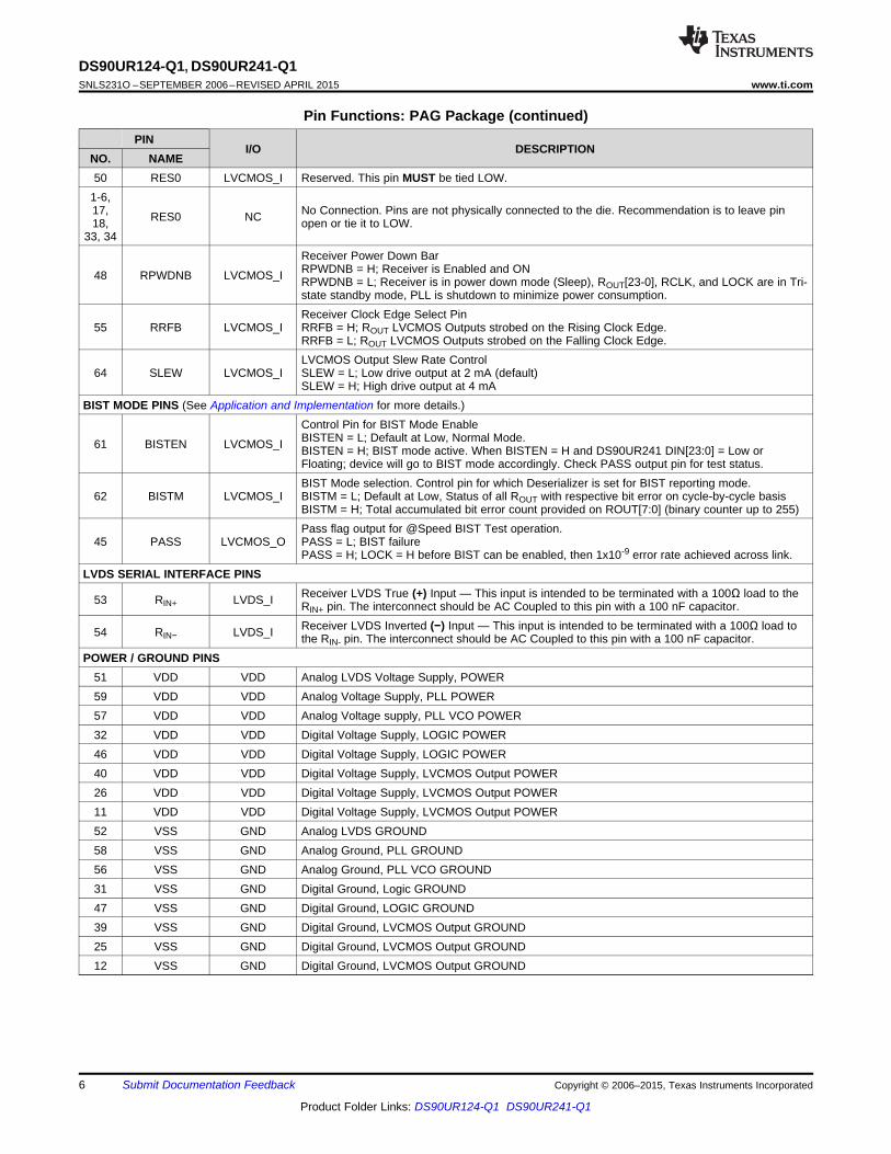
Pin Functions: PAG PackagePIN
I/O DESCRIPTIONNO. NAME
LVCMOS PARALLEL INTERFACE PINS24 RCLK LVCMOS_O Parallel Interface Clock Output Pin. Strobe edge set by RRFB configuration pin.
35-38, ROUT[7:0] LVCMOS_O Receiver Parallel Interface Data Outputs – Group 141-4419-22, ROUT[15:8] LVCMOS_O Receiver Parallel Interface Data Outputs – Group 227-307-10, ROUT[23:16] LVCMOS_O Receiver Parallel Interface Data Outputs – Group 313-16
CONTROL AND CONFIGURATION PINSLOCK indicates the status of the receiver PLL
23 LOCK LVCMOS_O LOCK = H; receiver PLL is lockedLOCK = L; receiver PLL is unlocked, ROUT[23-0] and RCLK are at Tri-state.Progressive Turn On Operation SelectionPTO = H; ROUT[23:0] are grouped into three groups of eight, with each group switching about ±1
49 PTOSEL LVCMOS_I UI to ±2 UI apart relative to RCLK. (Figure 17)PTO = L; PTO Spread Mode, ROUT[23:0] outputs are spread ±1 UI to ±2 UI and RCLK spread ±1UI. (Figure 18) See Applications Informations section for more details.Randomizer Control Input Pin (See Table 2 for more details.)
63 RAOFF LVCMOS_I RAOFF = H, Backwards compatible mode for use with DS90C241 Serializer.RAOFF = L; Additional randomization ON (Default), Selects 2E7 LSFR setting.Receiver Data EnableREN = H; ROUT[23-0] and RCLK are Enabled (ON).60 REN LVCMOS_I REN = L; ROUT[23-0] and RCLK are Disabled (OFF), Receiver ROUT[23-0] and RCLK Outputs arein Tri-state, PLL still operational and locked to TCLK.
Copyright © 2006–2015, Texas Instruments Incorporated Submit Documentation Feedback 5
Product Folder Links: DS90UR124-Q1 DS90UR241-Q1
DS90UR124-Q1, DS90UR241-Q1SNLS231O –SEPTEMBER 2006–REVISED APRIL 2015 www.ti.com
Pin Functions: PAG Package (continued)PIN
I/O DESCRIPTIONNO. NAME50 RES0 LVCMOS_I Reserved. This pin MUST be tied LOW.
1-6,17, No Connection. Pins are not physically connected to the die. Recommendation is to leave pinRES0 NC18, open or tie it to LOW.
33, 34Receiver Power Down BarRPWDNB = H; Receiver is Enabled and ON48 RPWDNB LVCMOS_I RPWDNB = L; Receiver is in power down mode (Sleep), ROUT[23-0], RCLK, and LOCK are in Tri-state standby mode, PLL is shutdown to minimize power consumption.Receiver Clock Edge Select Pin
55 RRFB LVCMOS_I RRFB = H; ROUT LVCMOS Outputs strobed on the Rising Clock Edge.RRFB = L; ROUT LVCMOS Outputs strobed on the Falling Clock Edge.LVCMOS Output Slew Rate Control
64 SLEW LVCMOS_I SLEW = L; Low drive output at 2 mA (default)SLEW = H; High drive output at 4 mA
BIST MODE PINS (See Application and Implementation for more details.)Control Pin for BIST Mode EnableBISTEN = L; Default at Low, Normal Mode.61 BISTEN LVCMOS_I BISTEN = H; BIST mode active. When BISTEN = H and DS90UR241 DIN[23:0] = Low orFloating; device will go to BIST mode accordingly. Check PASS output pin for test status.BIST Mode selection. Control pin for which Deserializer is set for BIST reporting mode.
62 BISTM LVCMOS_I BISTM = L; Default at Low, Status of all ROUT with respective bit error on cycle-by-cycle basisBISTM = H; Total accumulated bit error count provided on ROUT[7:0] (binary counter up to 255)Pass flag output for @Speed BIST Test operation.
45 PASS LVCMOS_O PASS = L; BIST failurePASS = H; LOCK = H before BIST can be enabled, then 1x10⁻⁹ error rate achieved across link.
LVDS SERIAL INTERFACE PINSReceiver LVDS True (+) Input — This input is intended to be terminated with a 100Ω load to the53 RIN+ LVDS_I RIN+ pin. The interconnect should be AC Coupled to this pin with a 100 nF capacitor.Receiver LVDS Inverted (−) Input — This input is intended to be terminated with a 100Ω load to54 RIN− LVDS_I the RIN- pin. The interconnect should be AC Coupled to this pin with a 100 nF capacitor.
POWER / GROUND PINS51 VDD VDD Analog LVDS Voltage Supply, POWER59 VDD VDD Analog Voltage Supply, PLL POWER57 VDD VDD Analog Voltage supply, PLL VCO POWER32 VDD VDD Digital Voltage Supply, LOGIC POWER46 VDD VDD Digital Voltage Supply, LOGIC POWER40 VDD VDD Digital Voltage Supply, LVCMOS Output POWER26 VDD VDD Digital Voltage Supply, LVCMOS Output POWER11 VDD VDD Digital Voltage Supply, LVCMOS Output POWER52 VSS GND Analog LVDS GROUND58 VSS GND Analog Ground, PLL GROUND56 VSS GND Analog Ground, PLL VCO GROUND31 VSS GND Digital Ground, Logic GROUND47 VSS GND Digital Ground, LOGIC GROUND39 VSS GND Digital Ground, LVCMOS Output GROUND25 VSS GND Digital Ground, LVCMOS Output GROUND12 VSS GND Digital Ground, LVCMOS Output GROUND
6 Submit Documentation Feedback Copyright © 2006–2015, Texas Instruments Incorporated
Product Folder Links: DS90UR124-Q1 DS90UR241-Q1

DS90UR124-Q1, DS90UR241-Q1www.ti.com SNLS231O –SEPTEMBER 2006–REVISED APRIL 2015
7 Specifications
7.1 Absolute Maximum Ratingsover operating free-air temperature range (unless otherwise noted) (1)
MIN MAX UNITSupply Voltage (VDD) –0.3 4 VLVCMOS Input Voltage –0.3 VDD +0.3 VLVCMOS Output Voltage –0.3 VDD +0.3 VLVDS Receiver Input Voltage –0.3 +3.9 VLVDS Driver Output Voltage –0.3 +3.9 VLVDS Output Short Circuit Duration 10 msJunction Temperature 150 °CLead Temperature (Soldering, 4 seconds) 260 °C
45.8 (4L);RθJADS90UR241 − 48L 75.4 (2L)TQFP
RθJC 21.0Maximum Package Power Package °C/WDissipation Capacity (2) Derating: 42.8 (4L);RθJADS90UR124 − 64L 67.2 (2L)TQFP
RθJC 14.6Storage temperature, Tstg –65 150 °C
(1) Stresses beyond those listed under Absolute Maximum Ratings may cause permanent damage to the device. These are stress ratingsonly, which do not imply functional operation of the device at these or any other conditions beyond those indicated under RecommendedOperating Conditions. Exposure to absolute-maximum-rated conditions for extended periods may affect device reliability.
(2) 1/RθJA °C/W above +25°C
7.2 ESD RatingsVALUE UNIT
DS90UR241-Q1 IN PFB PACKAGEHuman body model (HBM), per AEC ≥±8000All pinsQ100-002 (1)
Corner pins (1, 12, 13, 24, 25, 36, ±12500Charged device model (CDM), per 37, and 48)V(ESD) Electrostatic discharge VAEC Q100-011
Other pins ±12500Contact Discharge (20, 19) ±10000
(ISO10605) (2)Air Discharge (20, 19) ±30000
DS90UR124-Q1 IN PAG PACKAGEHuman body model (HBM), per AEC All pins ≥±8000Q100-002 (1)
Corner pins (1, 16, 17, 32, 33, 48, ±12500Charged device model (CDM), per 49, and 64)V(ESD) Electrostatic discharge VAEC Q100-011
Other pins ±12500Contact Discharge (RIN+, RIN−) ±10000
(ISO10605) (2)Air Discharge (RIN+, RIN−) ±30000
(1) AEC Q100-002 indicates HBM stressing is done in accordance with the ANSI/ESDA/JEDEC JS-001 specification.(2) RD = 2 kΩ, CS = 330 pF
7.3 Recommended Operating Conditionsover operating free-air temperature range (unless otherwise noted)
MIN NOM MAX UNITSupply Voltage (VDD) 3.0 3.3 3.6 VOperating Free Air Temperature (TA) –40 25 105 °CClock Rate 5 43 MHzSupply Noise ±100 mVP-P
Copyright © 2006–2015, Texas Instruments Incorporated Submit Documentation Feedback 7
Product Folder Links: DS90UR124-Q1 DS90UR241-Q1

DS90UR124-Q1, DS90UR241-Q1SNLS231O –SEPTEMBER 2006–REVISED APRIL 2015 www.ti.com
7.4 Thermal InformationDS90UR124-Q1 DS90UR241-Q1
THERMAL METRIC (1) PAG [TQFP] PFB [TQFP] UNIT64 PINS 48 PINS
RθJA Junction-to-ambient thermal resistance 58.1 64.3RθJC(top) Junction-to-case (top) thermal resistance 13.0 14.1RθJB Junction-to-board thermal resistance 30.4 30.2 °C/WψJT Junction-to-top characterization parameter 0.3 0.4ψJB Junction-to-board characterization parameter 30.0 29.8
(1) For more information about traditional and new thermal metrics, see the IC Package Thermal Metrics application report, SPRA953.
7.5 Electrical Characteristicsover recommended operating supply and temperature ranges unless otherwise specified
PARAMETER TEST CONDITIONS PIN/FREQ. MIN TYP MAX UNITLVCMOS DC SPECIFICATIONSVIH High-Level Input Voltage Tx: DIN[0:23], TCLK, 2 VDD V
TPWDNB, DEN, TRFB,VIL Low-Level Input Voltage GND 0.8 VRAOFF, VODSEL, RES0.Rx: RPWDNB, RRFB, REN,
VCL Input Clamp Voltage ICL = −18 mA –0.8 –1.5 VPTOSEL, BISTEN, BISTM,SLEW, RES0.Tx: DIN[0:23], TCLK,TPWDNB, DEN, TRFB,RAOFF, RES0. –10 ±2 10Rx: RRFB, REN, PTOSEL,IIN Input Current VIN = 0 V or 3.6 V µABISTEN, BISTM, SLEW,RES0.Rx: RPWDNB –20 ±5 20
High-Level Output IOH = −2 mA, SLEW = LVOH 2.3 3 VDD VVoltage IOH = −4 mA, SLEW = HLow-Level Output IOL = 2 mA, SLEW = L Rx: ROUT[0:23], RCLK,VOL GND 0.33 0.5 VVoltage IOL = 4 mA, SLEW = H LOCK, PASS.Output Short CircuitIOS VOUT = 0 V –40 –70 –110 mACurrent
RPWDNB, REN = 0 V, Rx: ROUT[0:23], RCLK,IOZ Tri-state Output Current –30 ±0.4 30 µAVOUT = 0 V or VDD LOCK, PASS.LVDS DC SPECIFICATIONS
Differential ThresholdVTH 50 mVHigh VoltageVCM = 1.8 V
Differential ThresholdVTL –50 mVRx: RIN+, RIN−Low VoltageVIN = 2.4 V, VDD = 3.6 V ±100 ±250
IIN Input Current µAVIN = 0 V, VDD = 3.6 V ±100 ±250
8 Submit Documentation Feedback Copyright © 2006–2015, Texas Instruments Incorporated
Product Folder Links: DS90UR124-Q1 DS90UR241-Q1

DS90UR124-Q1, DS90UR241-Q1www.ti.com SNLS231O –SEPTEMBER 2006–REVISED APRIL 2015
Electrical Characteristics (continued)over recommended operating supply and temperature ranges unless otherwise specified
PARAMETER TEST CONDITIONS PIN/FREQ. MIN TYP MAX UNITRL = 100 Ω, without VODSEL = L 380 500 630Output DifferentialVOD pre-emphasis mVVoltage (DOUT+)–(DOUT−) VODSEL = H 500 900 1100Figure 12
VODSEL = LOutput Differential RL = 100 Ω,ΔVOD 1 50 mVVoltage Unbalance without pre-emphasis VODSEL = HVODSEL = LRL = 100 Ω,VOS Offset Voltage 1 1.25 1.50 Vwithout pre-emphasis VODSEL = HVODSEL = LOffset Voltage RL = 100 Ω,ΔVOS 3 50 mVUnbalance without pre-emphasis VODSEL = H Tx: DOUT+, DOUT−VODSEL = L –2 –5 –8Output Short Circuit DOUT = 0 V, DIN = H,IOS mACurrent TPWDNB = 2.4 V VODSEL = H –4.5 –7.9 –14
TPWDNB = 0 V, –15 ±1 15DOUT = 0 V OR VDD
TPWDNB = 2.4 V, DEN = 0 V –15 ±1 15IOZ Tri-state Output Current DOUT = 0 V OR VDD µATPWDNB = 2.4 V, DEN = 2.4 V,DOUT = 0 V OR VDD –15 ±1 15NO LOCK (NO TCLK)
SER/DES SUPPLY CURRENT (DVDD*, PVDD* AND AVDD* PINS) *DIGITAL, PLL, AND ANALOG VDDSf = 43 MHz,RL = 100 Ω, PRE = OFF, checkerboard pattern 60 85RAOFF = H, VODSEL = L Figure 3Serializer
IDDT Total Supply Current RL = 100 Ω, PRE = 12 kΩ, mA65 90(includes load current) RAOFF = H, VODSEL = LRL = 100 Ω, PRE = OFF, f = 43 MHz, 66 90RAOFF = H, VODSEL = H random pattern
Serializer TPWDNB = 0VIDDTZ Supply Current Power- 45 µA(All other LVCMOS Inputs = 0 V)downf = 43 MHz,CL = 4 pF, checkerboard pattern 85 105SLEW = HDeserializer LVCMOS Output Figure 4
IDDR Total Supply Current mAf = 43 MHz,(includes load current) CL = 4 pF, random pattern 80 100SLEW = H LVCMOS Output
Deserializer RPWDNB = 0 VIDDRZ Supply Current Power- (All other LVCMOS Inputs = 0 V, 50 µA
down RIN+/RIN- = 0 V)
Copyright © 2006–2015, Texas Instruments Incorporated Submit Documentation Feedback 9
Product Folder Links: DS90UR124-Q1 DS90UR241-Q1

DS90UR124-Q1, DS90UR241-Q1SNLS231O –SEPTEMBER 2006–REVISED APRIL 2015 www.ti.com
7.6 Serializer Input Timing Requirements for TCLKover recommended operating supply and temperature ranges unless otherwise specified
MIN NOM MAX UNITtTCP Transmit Clock Period Figure 7 23.25 T 200 nstTCIH Transmit Clock High Time 0.3 T 0.5 T 0.7 T nstTCIL Transmit Clock Low Time 0.3 T 0.5 T 0.7 T nstCLKT TCLK Input Transition Time Figure 6 2.5 ns
f = 43 MHz ±100tJIT TCLK Input Jitter ps
f = 33 MHz ±130
7.7 Serializer Switching Characteristicsover recommended operating supply and temperature ranges unless otherwise specified
PARAMETER TEST CONDITIONS MIN TYP MAX UNITtLLHT LVDS Low-to-High Transition Time 245 550 psRL = 100 Ω, VODSEL = L,
CL = 10 pF to GND, Figure 5tLHLT LVDS High-to-Low Transition Time 264 550 pstDIS DIN (0:23) Setup to TCLK 4 nsRL = 100 Ω, CL = 10 pF to GND
Figure 7tDIH DIN (0:23) Hold from TCLK 4 nstHZD DOUT ± HIGH to Tri-state Delay 10 15 ns
RL = 100 Ω,tLZD DOUT ± LOW to Tri-state Delay 10 15 nsCL = 10 pF to GND
tZHD DOUT ± Tri-state to HIGH Delay 75 150 nsFigure 8tZLD DOUT ± Tri-state to LOW Delay 75 150 nstPLD Serializer PLL Lock Time RL = 100 Ω 10 ms
RL = 100 Ω, PRE = OFF,RAOFF = L, TRFB = H, 3.5T+2 3.5T+10Figure 10
tSD Serializer Delay nsRL = 100 Ω, PRE = OFF,RAOFF = L, TRFB = L, 3.5T+2 3.5T+10Figure 105 MHz–43 MHz,
TxOUT TxOUT_Eye_Opening. RL = 100 Ω, CL = 10 pF to GND, 0.76 0.84 UI_E_O TxOUT_E_O centered on (tBIT/)2 RANDOM patternFigure 11
7.8 Deserializer Switching Characteristicsover recommended operating supply and temperature ranges unless otherwise specified
PARAMETER TEST CONDITIONS PIN/FREQ. MIN TYP MAX UNITtRCP = tTCP,tRCP Receiver out Clock Period 23.25 T 200 nsPTOSEL = H RCLK
Figure 17PTOSEL = H,tRDC RCLK Duty Cycle 45% 50% 55%SLEW = LLVCMOS Low-to-High TransitiontCLH 1.5 2.5 nsCL = 4 pFTime ROUT [0:23],(lumped load), RCLK, LOCKLVCMOS High-to-Low Transition SLEW = HtCHL 1.5 2.5 nsTimeLVCMOS Low-to-High TransitiontCLH 2.0 3.5 nsCL = 4 pFTime ROUT [0:23],(lumped load), RCLK, LOCKLVCMOS High-to-Low Transition SLEW = LtCHL 2.0 3.5 nsTimeROUT (0:7) Setup Data to RCLK (0.5×tRCP)–tROS (0.35)× tRCP nsPTOSEL = L,(Group 1) 3 UI
SLEW = H, ROUT[0:7]ROUT (0:7) Hold Data to RCLK (0.5×tRCP)–Figure 18tROH (0.35)× tRCP ns(Group 1) 3 UI
10 Submit Documentation Feedback Copyright © 2006–2015, Texas Instruments Incorporated
Product Folder Links: DS90UR124-Q1 DS90UR241-Q1

TCLK
ODD DIN
EVEN DIN
Signal PatternDevice Pin Name
DS90UR124-Q1, DS90UR241-Q1www.ti.com SNLS231O –SEPTEMBER 2006–REVISED APRIL 2015
Deserializer Switching Characteristics (continued)over recommended operating supply and temperature ranges unless otherwise specified
PARAMETER TEST CONDITIONS PIN/FREQ. MIN TYP MAX UNITROUT (8:15) Setup Data to RCLK (0.5×tRCP)–tROS (0.35)× tRCP ns(Group 2) 3 UIROUT [8:15],
LOCKROUT (8:15) Hold Data to RCLK (0.5×tRCP)–tROH (0.35)× tRCP nsPTOSEL = L,(Group 2) 3 UISLEW = H,
ROUT (16:23) Setup Data to RCLK (0.5×tRCP)–Figure 18tROS (0.35)× tRCP ns(Group 3) 3 UIROUT [16:23]
ROUT (16:23) Setup Data to RCLK (0.5×tRCP)–tROH (0.35)× tRCP ns(Group 3) 3 UIROUT (0:7) Setup Data to RCLK (0.5×tRCP)–tROS (0.35)× tRCP ns(Group 1) 2 UI
ROUT[0:7]ROUT (0:7) Hold Data to RCLK (0.5×tRCP)+tROH (0.35)× tRCP ns(Group 1) 2 UIROUT (8:15) Setup Data to RCLK (0.5×tRCP)−tROS (0.35)× tRCP nsPTOSEL = H,(Group 2) 1 UIROUT [8:15],SLEW = H, LOCKROUT (8:15) Hold Data to RCLK (0.5×tRCP)+Figure 17tROH (0.35)× tRCP ns(Group 2) 1 UIROUT (16:23) Setup Data to RCLK (0.5×tRCP)+tROS (0.35)× tRCP ns(Group 3) 1 UI
ROUT [16:23]ROUT (16:23) Setup Data to RCLK (0.5×tRCP)–tROH (0.35)× tRCP ns(Group 3) 1 UI
tHZR HIGH to Tri-state Delay 3 10 nstLZR LOW to Tri-state Delay 3 10 nsPTOSEL = H, ROUT [0:23],
Figure 16 RCLK, LOCKtZHR Tri-state to HIGH Delay 3 10 nstZLR Tri-state to LOW Delay 3 10 ns
PTOSEL = H, [5+(5/56)]T [5+(5/56)]TtDD Deserializer Delay RCLK nsFigure 14 +3.7 +85 MHz 128k*TDeserializer PLL Lock Time fromtDSR See Figure 16 msPowerdown 43 MHz 128k*T
RxIN_T SeeReceiver INput TOLerance Left 5 MHz–43 MHz 0.25 UIOL-L Figure 19RxIN_T SeeReceiver INput TOLerance Right 5 MHz–43 MHz 0.25 UIOL-R Figure 19
Figure 3. Serializer Input Checkerboard Pattern
Copyright © 2006–2015, Texas Instruments Incorporated Submit Documentation Feedback 11
Product Folder Links: DS90UR124-Q1 DS90UR241-Q1

SetupVDD/2 Hold
tDIHtDIS
TCLK
DIN [0:23]
tTCP
0V
VDD/2
VDD/2 VDD/2VDD/2
VDD
80%
20%
80%
20%
tCLKT tCLKT
TCLK
VDD
0V
80%
20%
80%
20%Vdiff = 0V
tLLHT tLHLT
Vdiff
Vdiff = (DOUT+) - (DOUT-)
100:
DOUT+
DOUT-10 pF
10 pF
RCLK
ODD ROUT
EVEN ROUT
Signal PatternDevice Pin Name
DS90UR124-Q1, DS90UR241-Q1SNLS231O –SEPTEMBER 2006–REVISED APRIL 2015 www.ti.com
Figure 4. Deserializer Output Checkerboard Pattern
Figure 5. Serializer LVDS Output Load and Transition Times
Figure 6. Serializer Input Clock Transition Times
Figure 7. Serializer Setup and Hold Times
12 Submit Documentation Feedback Copyright © 2006–2015, Texas Instruments Incorporated
Product Folder Links: DS90UR124-Q1 DS90UR241-Q1

2.0V 0.8V
TCLK
DOUT±
tHZD or
tLZD
tZHD or
tZLD
Output Active
tPLD
PWDWN
TRI-STATE TRI-STATE
DEN
DOUT-
DOUT+5 pF
100:
Parasitic package andTrace capacitance
200 mV DCADCA DCA DCA
$OOGDWD³0´V
CLK1
tZLD
tTCP
DCADCADCADCA
CLK1
tTCP
200 mV
DEN(single-ended)
200 mV DCADCA DCA DCA
$OOGDWD³1´V
CLK0
tZHD
tTCP
DCADCADCADCA
CLK0
tTCP
200 mV
DOUT±(differential)
VCC/2
0V
DOUT±(differential)
0V
VCC/2
tHZD
DEN(single-ended)
VCC/2
0V 0V
VCC/2
tLZD
DS90UR124-Q1, DS90UR241-Q1www.ti.com SNLS231O –SEPTEMBER 2006–REVISED APRIL 2015
Figure 8. Serializer Tri-State Test Circuit and Delay
Figure 9. Serializer PLL Lock Time, and TPWDNB Tri-State Delays
Copyright © 2006–2015, Texas Instruments Incorporated Submit Documentation Feedback 13
Product Folder Links: DS90UR124-Q1 DS90UR241-Q1

80%
20%
80%
20%
tCLH
Deserializer
4 pFlumped
tCHL
PA
RA
LLE
L-T
O-S
ER
IAL
DOUT+
DOUT-
24
DIN RL
TCLK
20194528
Ideal Center Position (tBIT/2)
tBIT (1 UI)
Ideal Data Bit End
Ideal Data Bit Beginning
tBIT(1/2 UI) tBIT(1/2 UI)
TxOUT_E_O
23210
||
START
BIT
STOP
BITSYMBOL N
23210
||
START
BIT
STOP
BITSYMBOL N-1
23210
||
START
BIT
STOP
BITSYMBOL N-2
23210
||
START
BIT
STOP
BITSYMBOL N-3
23210
STOP
BITSYMBOL N-4
||
DOUT0-23
DCA, DCB
|
TCLK
tSD
DIN SYMBOL N+1SYMBOL N SYMBOL N+2 SYMBOL N+3
||
DS90UR124-Q1, DS90UR241-Q1SNLS231O –SEPTEMBER 2006–REVISED APRIL 2015 www.ti.com
Figure 10. Serializer Delay
Figure 11. Transmitter Output Eye Opening (TxOUT_E_O)
VOD = (DOUT+) – (DOUT−)Differential output signal is shown as (DOUT+) – (DOUT−), device in Data Transfer mode.
Figure 12. Serializer VOD Diagram
Figure 13. Deserializer LVCMOS Output Load and Transition Times
14 Submit Documentation Feedback Copyright © 2006–2015, Texas Instruments Incorporated
Product Folder Links: DS90UR124-Q1 DS90UR241-Q1

VOH
REN
VOL + 0.5VVOL
ROUT [23:0]
VOL + 0.5V
tLZR
500:
VREF = VDD/2 for tZLR or tLZR,
VOH - 0.5V VOH + 0.5V
tZLR
tHZR tZHR
VDD/2 VDD/2
VOH
VOL
REN
VREF+- VREF = 0V for tZHR or tHZRCL = 8 pF
NOTE:
CL includes instrumentation and fixture capacitance within 6 cm of ROUT [23:0].
23210
||
START
BIT
STOP
BITSYMBOL N+3
23210
||
START
BIT
STOP
BITSYMBOL N+2
23210
||
START
BIT
STOP
BITSYMBOL N+1
23210
||
START
BIT
STOP
BITSYMBOL N
RIN0-23
DCA, DCB
RCLK
tDD
ROUT0-23 SYMBOL N-1 SYMBOL NSYMBOL N-2SYMBOL N-3
DS90UR124-Q1, DS90UR241-Q1www.ti.com SNLS231O –SEPTEMBER 2006–REVISED APRIL 2015
Figure 14. Deserializer Delay
Figure 15. Deserializer Tri-State Test Circuit and Timing
Copyright © 2006–2015, Texas Instruments Incorporated Submit Documentation Feedback 15
Product Folder Links: DS90UR124-Q1 DS90UR241-Q1

ROUT [7:0]
(group 1)
ROUT [15:8]
(group 2)
Data ValidBefore RCLK
Data ValidAfter RCLK VDD/2
ROUT [23:16]
(group 3)
RCLKtRDC tRDC
tROS tROH
tROS tROH
tROS tROH
VDD/2
VDD/2VDD/2
VDD/2VDD/2
VDD/2VDD/2
| -2 UI
| -1 UI
| +2 UI
| +1 UI
| +1 UI | -1 UI
tRCP
Data ValidBefore RCLK
Data ValidAfter RCLK
Data ValidBefore RCLK
Data ValidAfter RCLK
RIN±
||
TRI-STATE
TRI-STATE
TRI-STATE
TRI-STATE
TRI-STATE
ROUT [0:23]
RCLK
TRI-STATELOCK
v[
tHZR or tLZR
tDSR
REN
PWDN2.0V
0.8V
DS90UR124-Q1, DS90UR241-Q1SNLS231O –SEPTEMBER 2006–REVISED APRIL 2015 www.ti.com
Figure 16. Deserializer PLL Lock Times and RPWDNB Tri-State Delay
Figure 17. Deserializer Setup and Hold Times and PTO, PTOSEL = H
16 Submit Documentation Feedback Copyright © 2006–2015, Texas Instruments Incorporated
Product Folder Links: DS90UR124-Q1 DS90UR241-Q1

Mag
nitu
de (
100
mV
/DIV
)
Time (2.5 ns/DIV)
Mag
nitu
de (
500
mV
/DIV
)
Time (5 ns/DIV)
tBIT (1 UI)
Sampling Window
Ideal Data Bit End
Ideal Data Bit Beginning
RxIN_TOL -L RxIN_TOL -R
Ideal Center Position (tBIT/2)
½ Symbol
RCLK
½ Symbol
ROUT
(Ideal)
ROUT
GRP1 1 + 3/28 Symbol 1 - 2/28 Symbol 1 + 3/28 Symbol 1 - 4/28 Symbol
2 UI EARLY 1 UI LATE 1 UI EARLY 2 UI LATE 2 UI EARLY
DS90UR124-Q1, DS90UR241-Q1www.ti.com SNLS231O –SEPTEMBER 2006–REVISED APRIL 2015
Group 1 will be latched internally by sequence of (early 2UI, late 1UI, early 1UI, late 2UI).Group 2 will be latched internally by sequence of (late 1UI, early 1UI, late 2UI, early 2UI).Group 3 will be latched internally by sequence of (early 1UI, late 2UI, early 2UI, late 1UI).
Figure 18. Deserializer Setup and Hold Times and PTO Spread, PTOSEL = L
RxIN_TOL_L is the ideal noise margin on the left of the figure, with respect to ideal.RxIN_TOL_R is the ideal noise margin on the right of the figure, with respect to ideal.
Figure 19. Receiver Input Tolerance (RxIN_TOL) and Sampling Window
7.9 Typical Characteristics
Figure 20. DS90UR241 DOUT± With PCLK at 43 MHz Figure 21. DS90UR124 PCLK Output at 43 MHzMeasured at RIN± Termination
Copyright © 2006–2015, Texas Instruments Incorporated Submit Documentation Feedback 17
Product Folder Links: DS90UR124-Q1 DS90UR241-Q1

DENRAOFF
DIN
TRFB
24
REN
RAOFFTCLK
TPWDNB
SERIALIZER ± DS90UR241
PLL
Timingand
Control
DOUT-
RT =
100:
RT
= 1
00:RIN-
DESERIALIZER ± DS90UR124
DOUT+ RIN+
PLL Timingand
Control
24ROUT
LOCK
RCLKClockRecovery
Out
put L
atch
Ser
ial t
o P
aral
lel
DC
Bal
ance
Dec
oder
Inpu
t Lat
ch
Par
alle
l to
Ser
ial
DC
Bal
ance
Enc
oder
PRE
PASS
RRFBRPWDNB
BISTENBISTMSLEW
PTOSEL
VODSEL
DS90UR124-Q1, DS90UR241-Q1SNLS231O –SEPTEMBER 2006–REVISED APRIL 2015 www.ti.com
8 Detailed Description
8.1 OverviewThe DS90UR241 Serializer and DS90UR124 Deserializer chipset is an easy-to-use transmitter and receiver pairthat sends 24-bits of parallel LVCMOS data over a single serial LVDS link from 120 Mbps to 1.03 Gbpsthroughput. The DS90UR241 transforms a 24-bit wide parallel LVCMOS data into a single high speed LVDSserial data stream with embedded clock and scrambles / DC Balances the data to enhance signal quality tosupport AC coupling. The DS90UR124 receives the LVDS serial data stream and converts it back into a 24-bitwide parallel data and recovered clock. The 24-bit Serializer/Deserializer chipset is designed to transmit data upto 10 meters over shielded twisted pair (STP) at clock speeds from 5 MHz to 43 MHz.
The Deserializer can attain lock to a data stream without the use of a separate reference clock source, greatlysimplifying system complexity and overall cost. The Deserializer synchronizes to the Serializer regardless of datapattern, delivering true automatic “plug and lock” performance. It will lock to the incoming serial stream withoutthe need of special training patterns or sync characters. The Deserializer recovers the clock and data byextracting the embedded clock information and validating data integrity from the incoming data stream and thendeserializes the data. The Deserializer monitors the incoming clock information, determines lock status, andasserts the LOCK output high when lock occurs.
In addition, the Deserializer also supports an optional @SPEED BIST (Built In Self Test) mode, BIST error flag,and LOCK status reporting pin. Signal quality on the wide parallel output is controlled by the SLEW control andbank slew (PTOSEL) inputs to help reduce noise and system EMI. Each device has a power down control toenable efficient operation in various applications.
8.2 Functional Block Diagram
8.3 Feature Description
8.3.1 Initialization and Locking MechanismInitialization of the DS90UR241 and DS90UR124 must be established before each device sends or receivesdata. Initialization refers to synchronizing the Serializer’s and Deserializer’s PLL’s together. After the Serializerslocks to the input clock source, the Deserializer synchronizes to the Serializers as the second and finalinitialization step.
18 Submit Documentation Feedback Copyright © 2006–2015, Texas Instruments Incorporated
Product Folder Links: DS90UR124-Q1 DS90UR241-Q1

DS90UR124-Q1, DS90UR241-Q1www.ti.com SNLS231O –SEPTEMBER 2006–REVISED APRIL 2015
Feature Description (continued)Step 1: When VDD is applied to both Serializer and/or Deserializer, the respective outputs are held in Tri-stateand internal circuitry is disabled by on-chip power-on circuitry. When VDD reaches VDD OK (approximately 2.2 V)the PLL in Serializer begins locking to a clock input. For the Serializer, the local clock is the transmit clock,TCLK. The Serializer outputs are held in Tri-state while the PLL locks to the TCLK. After locking to TCLK, theSerializer block is now ready to send data patterns. The Deserializer output will remain in Tri-state while its PLLlocks to the embedded clock information in serial data stream. Also, the Deserializer LOCK output will remain lowuntil its PLL locks to incoming data and sync-pattern on the RIN± pins.
Step 2: The Deserializer PLL acquires lock to a data stream without requiring the Serializer to send specialpatterns. The Serializer that is generating the stream to the Deserializer will automatically send random (non-repetitive) data patterns during this step of the Initialization State. The Deserializer will lock onto embedded clockwithin the specified amount of time. An embedded clock and data recovery (CDR) circuit locks to the incoming bitstream to recover the high-speed receive bit clock and re-time incoming data. The CDR circuit expects a codedinput bit stream. In order for the Deserializer to lock to a random data stream from the Serializer, it performs aseries of operations to identify the rising clock edge and validates data integrity, then locks to it. Because thislocking procedure is independent on the data pattern, total random locking duration may vary. At the point whenthe Deserializer’s CDR locks to the embedded clock, the LOCK pin goes high and valid RCLK/data appears onthe outputs. Note that the LOCK signal is synchronous to valid data appearing on the outputs. The Deserializer’sLOCK pin is a convenient way to ensure data integrity is achieved on receiver side.
8.3.2 Data TransferAfter Serializer lock is established, the inputs DIN0–DIN23 are used to input data to the Serializer. Data isclocked into the Serializer by the TCLK input. The edge of TCLK used to strobe the data is selectable via theTRFB pin. TRFB high selects the rising edge for clocking data and low selects the falling edge. The Serializeroutputs (DOUT±) are intended to drive point-to-point connections.
CLK1, CLK0, DCA, DCB are four overhead bits transmitted along the single LVDS serial data stream (Figure 30).The CLK1 bit is always high and the CLK0 bit is always low. The CLK1 and CLK0 bits function as the embeddedclock bits in the serial stream. DCB functions as the DC Balance control bit. It does not require any pre-coding ofdata on transmit side. The DC Balance bit is used to minimize the short and long-term DC bias on the signallines. This bit operates by selectively sending the data either unmodified or inverted. The DCA bit is used tovalidate data integrity in the embedded data stream. Both DCA and DCB coding schemes are integrated andautomatically performed within Serializer and Deserializer.
The chipset supports clock frequency ranges of 5 MHz to 43 MHz. Every clock cycle, 24 databits are sent alongwith 4 additional overhead control bits. Thus the line rate is 1.20 Gbps maximum (140Mbps minimum). The link isextremely efficient at 86% (24/28). Twenty five (24 data + 1 clock) plus associated ground signals are reduced toonly 1 single LVDS pair providing a compression ratio of better then 25 to 1.
In the serialized data stream, data/embedded clock & control bits (24+4 bits) are transmitted from the Serializerdata output (DOUT±) at 28 times the TCLK frequency. For example, if TCLK is 43 MHz, the serial rate is 43 × 28= 1.20 Giga bits per second. Since only 24 bits are from input data, the serial “payload” rate is 24 times theTCLK frequency. For instance, if TCLK = 43 MHz, the payload data rate is 43 x 24 = 1.03 Gbps. TCLK isprovided by the data source and must be in the range of 5 MHz to 43 MHz nominal. The Serializer outputs(DOUT±) can drive a point-to-point connection as shown in Figure 29. The outputs transmit data when the enablepin (DEN) is high and TPWDNB is high. The DEN pin may be used to Tri-state the outputs when driven low.
When the Deserializer channel attains lock to the input from a Serializer, it drives its LOCK pin high andsynchronously delivers valid data and recovered clock on the output. The Deserializer locks onto the embeddedclock, uses it to generate multiple internal data strobes, and then drives the recovered clock to the RCLK pin.The recovered clock (RCLK output pin) is synchronous to the data on the ROUT[23:0] pins. While LOCK is high,data on ROUT[23:0] is valid. Otherwise, ROUT[23:0] is invalid. The polarity of the RCLK edge is controlled by theRRFB input. ROUT[23:0], LOCK and RCLK outputs will each drive a maximum of 4-pF load with a 43-MHz clock.REN controls Tri-state for ROUTn and the RCLK pin on the Deserializer.
Copyright © 2006–2015, Texas Instruments Incorporated Submit Documentation Feedback 19
Product Folder Links: DS90UR124-Q1 DS90UR241-Q1

DS90UR124-Q1, DS90UR241-Q1SNLS231O –SEPTEMBER 2006–REVISED APRIL 2015 www.ti.com
Feature Description (continued)8.3.3 ResynchronizationIf the Deserializer loses lock, it will automatically try to re-establish lock. For example, if the embedded clockedge is not detected one time in succession, the PLL loses lock and the LOCK pin is driven low. The Deserializerthen enters the operating mode where it tries to lock to a random data stream. It looks for the embedded clockedge, identifies it, and then proceeds through the locking process.
The logic state of the LOCK signal indicates whether the data on ROUT is valid; when it is high, the data is valid.The system may monitor the LOCK pin to determine whether data on the ROUT is valid.
8.3.4 PowerdownThe Powerdown state is a low power sleep mode that the Serializer and Deserializer may use to reduce powerwhen no data is being transferred. The TPWDNB and RPWDNB are used to set each device into powerdownmode, which reduces supply current to the µA range. The Serializer enters powerdown when the TPWDNB pin isdriven low. In powerdown, the PLL stops and the outputs go into Tri-state, disabling load current and reducingcurrent supply. To exit Powerdown, TPWDNB must be driven high. When the Serializer exits Powerdown, its PLLmust lock to TCLK before it is ready for the Initialization state. The system must then allow time for Initializationbefore data transfer can begin. The Deserializer enters powerdown mode when RPWDNB is driven low. Inpowerdown mode, the PLL stops and the outputs enter Tri-state. To bring the Deserializer block out of thepowerdown state, the system drives RPWDNB high.
Both the Serializer and Deserializer must reinitialize and relock before data can be transferred. The Deserializerwill initialize and assert LOCK high when it is locked to the embedded clock.
8.3.5 Tri-StateFor the Serializer, Tri-state is entered when the DEN or TPWDNB pin is driven low. This will Tri-state both driveroutput pins (DOUT+ and DOUT−). When DEN is driven high, the serializer will return to the previous state aslong as all other control pins remain static (TPWDNB, TRFB).
When you drive the REN or RPWDNB pin low, the Deserializer enters Tri-state. Consequently, the receiveroutput pins (ROUT0–ROUT23) and RCLK will enter Tri-state. The LOCK output remains active, reflecting thestate of the PLL. The Deserializer input pins are high impedance during receiver powerdown (RPWDNB low) andpower-off (VDD = 0 V).
8.3.6 Pre-EmphasisThe DS90UR241 features a Pre-Emphasis function used to compensate for long or lossy transmission media.Cable drive is enhanced with a user selectable Pre-Emphasis feature that provides additional output currentduring transitions to counteract cable loading effects. The transmission distance will be limited by the losscharacteristics and quality of the media. Pre-Emphasis adds extra current during LVDS logic transition to reducethe cable loading effects and increase driving distance. In addition, Pre-Emphasis helps provide fastertransitions, increased eye openings, and improved signal integrity. The ability of the DS90UR241 to use the Pre-Emphasis feature will extend the transmission distance up to 10 meters in most cases.
To enable the Pre-Emphasis function, the “PRE” pin requires one external resistor (Rpre) to Vss in order to setthe additional current level. Values of Rpre should be between 6 kΩ and 100 MΩ. Values less than 6 kΩ shouldnot be used. A lower input resistor value on the ”PRE” pin increases the magnitude of dynamic current duringdata transition. The additional source current is based on the following formula: PRE = (RPRE ≥ 6 kΩ); IMAX = [48 /RPRE]. For example if Rpre = 15 kΩ , then the Pre-Emphasis current is increase by an additional 3.2 mA.
The amount of Pre-Emphasis for a given media will depend on the transmission distance of the application. Ingeneral, too much Pre-Emphasis can cause over or undershoot at the receiver input pins. This can result inexcessive noise, crosstalk and increased power dissipation. For short cables or distances, Pre-Emphasis maynot be required. Signal quality measurements are recommended to determine the proper amount of Pre-Emphasis for each application.
20 Submit Documentation Feedback Copyright © 2006–2015, Texas Instruments Incorporated
Product Folder Links: DS90UR124-Q1 DS90UR241-Q1

DS90UR124-Q1, DS90UR241-Q1www.ti.com SNLS231O –SEPTEMBER 2006–REVISED APRIL 2015
Feature Description (continued)8.3.7 AC-Coupling and TerminationThe DS90UR241 and DS90UR124 supports AC-coupled interconnects through integrated DC balancedencoding/decoding scheme. To use the Serializer and Deserializer in an AC-coupled application, insert externalAC-coupling capacitors in series in the LVDS signal path as illustrated in Figure 29. The Deserializer input stageis designed for AC-coupling by providing a built-in AC bias network which sets the internal VCM to +1.8V. With ACsignal coupling, capacitors provide the AC-coupling path to the signal input.
For the high-speed LVDS transmissions, the smallest available package should be used for the AC-couplingcapacitor. This will help minimize degradation of signal quality due to package parasitics. The most commonused capacitor value for the interface is a 100 nF (0.1 uF). NPO class 1 or X7R class 2 type capacitors arerecommended. 50 WVDC should be the minimum used for the best system-level ESD performance.
A termination resistor across DOUT± and RIN± is also required for proper operation to be obtained. Thetermination resistor should be equal to the differential impedance of the media being driven. This should be in therange of 90 to 132 Ω. 100 Ω is a typical value common used with standard 100-Ω transmission media. Thisresistor is required for control of reflections and also completes the current loop. It should be placed as close tothe Serializer DOUT± outputs and Deserializer RIN± inputs to minimize the stub length from the pins. To matchwith the deferential impedance on the transmission line, the LVDS I/O are terminated with 100-Ω resistors onSerializer DOUT± outputs pins and Deserializer RIN± input pins.
8.3.7.1 Receiver Termination Option 1A single 100-Ω termination resistor is placed across the RIN± pins (see Figure 29). This provides the signaltermination at the Receiver inputs. Other options may be used to increase noise tolerance.
8.3.7.2 Receiver Termination Option 2For additional EMI tolerance, two 50-Ω resistors may be used in place of the single 100-Ω resistor. A smallcapacitor is tied from the center point of the 50-Ω resistors to ground (see Figure 31). This provides a high-frequency low impedance path for noise suppression. Value is not critical, 4.7 nF may be used with generalapplications.
8.3.7.3 Receiver Termination Option 3For high noise environments, an additional voltage divider network may be connected to the center point. Thishas the advantage of a providing a DC low-impedance path for noise suppression. Use resistor values in therange of 100Ω-2KΩ for the pullup and pulldown. Ratio the resistor values to bias the center point at 1.8 V. Forexample (see Figure 32): VDD=3.3 V, Rpullup=1 KΩ, Rpulldown=1.2 KΩ; or Rpullup=100 Ω, Rpulldown=120 Ω(strongest). The smaller values will consume more bias current, but will provide enhanced noise suppression.
8.3.8 Signal Quality EnhancersThe DS90UR124 Deserializer supports two signal quality enhancers. The SLEW pin is used to increase the drivestrength of the LVCMOS outputs when driving heavy loads. SLEW allows output drive strength for high or lowcurrent drive. Default setting is LOW for low drive at 2 mA and HIGH for high drive at 4 mA.
There are two types of Progressive Turnon modes (Fixed and PTO Frequency Spread) to help reduce EMI:simultaneous switching noise and system ground bounce. The PTOSEL pin introduces bank skew in thedata/clock outputs to limit the number of outputs switching simultaneously. For Fixed-PTO mode, the DeserializerROUT[23:0] outputs are grouped into three groups of eight, with each group switching about 2 or 1 UI apart inphase from RCLK for Group 1 and Groups 2, 3, respectively (see Figure 17). In the PTO Frequency Spreadmode, ROUT[23:0] are also grouped into three groups of eight, with each group is separated out of phase withthe adjacent groups (see Figure 18) per every 4 cycles. Note that in the PTO Frequency Spread operating modeRCLK is also spreading and separated by 1 UI.
Copyright © 2006–2015, Texas Instruments Incorporated Submit Documentation Feedback 21
Product Folder Links: DS90UR124-Q1 DS90UR241-Q1

DS90UR124-Q1, DS90UR241-Q1SNLS231O –SEPTEMBER 2006–REVISED APRIL 2015 www.ti.com
Feature Description (continued)8.3.9 @SPEED-BIST Test FeatureTo assist vendors with test verification, the DS90UR241 and DS90UR124 is equipped with built-in self-test(BIST) capability to support both system manufacturing and field diagnostics. BIST mode is intended to check theentire high-speed serial link at full link-speed, without the use of specialized and expensive test equipment. Thisfeature provides a simple method for a system host to perform diagnostic testing of both Serializer andDeserializer. The BIST function is easily configured through the 2 control pins on the DS90UR124. When theBIST mode is activated, the Serializer has the ability to transfer an internally generated PRBS data pattern. Thispattern traverses across interconnecting links to the Deserializer. The DS90UR124 includes an on-chip PRBSpattern verification circuit that checks the data pattern for bit errors and reports any errors on the data output pinson the Deserializer.
The @SPEED-BIST feature uses 2 signal pins (BISTEN and BISTM) on the DS90UR124 Deserializer. TheBISTEN and BISTM pins together determine the functions of the BIST mode. The BISTEN signal (HIGH)activates the test feature on the Deserializer. After the BIST mode is enabled, all the data input channelsDIN[23:0] on the DS90UR241 Serializer must be set logic LOW or floating in order for Deserializer to startaccepting data. An input clock signal (TCLK) for the Serializer must also be applied during the entire BISToperation. The BISTM pin selects error reporting status mode of the BIST function. When BIST is configured inthe error status mode (BISTM = LOW), each of the ROUT[23:0] outputs will correspond to bit errors on a cycle-by-cycle basis. The result of bit mismatches are indicated on the respective parallel inputs on the ROUT[23:0]data output pins. In the BIST error-count accumulator mode (BISTM = HIGH), an 8-bit counter on ROUT[7:0] isused to represent the number of errors detected (0 to 255 max). The successful completion of the BIST test isreported on the PASS pin on the Deserializer. The Deserializer's PLL must first be locked to ensure the PASSstatus is valid. The PASS status pin will stay LOW and then transition to HIGH once a BER of 1x10⁻⁹ is achievedacross the transmission link.
8.3.10 Backward-Compatible Mode With DS90C241 and DS90C124The RAOFF pin allows a backward-compatible mode with DS90C241 and DS90C124 devices. To interface witheither DS90C241 Serializer or DS90C124 Deserializer, the RAOFF pin on DS90UR241 or DS90UR124 must betied HIGH to disable the additional LSFR coding. For normal operation directly with DS90UR241 to DS90UR124,RAOFF pins are set LOW. See Table 1 and Table 2 for more details.
22 Submit Documentation Feedback Copyright © 2006–2015, Texas Instruments Incorporated
Product Folder Links: DS90UR124-Q1 DS90UR241-Q1

DS90UR124-Q1, DS90UR241-Q1www.ti.com SNLS231O –SEPTEMBER 2006–REVISED APRIL 2015
8.4 Device Functional Modes
Table 1. DS90UR241 Serializer Truth TableTPWDNB DEN RAOFF Tx PLL Status LVDS Outputs
(Pin 9) (Pin 18) (Pin 12) (Internal) (Pins 19 and 20)L X X X Hi-ZH L X X Hi-ZH H X Not Locked Hi-ZH H L Locked Serialized Data with Embedded Clock
(DS90UR124 compatible)H H H Locked Serialized Data with Embedded Clock
(DS90C124 compatible)
Table 2. DS90UR124 Deserializer Truth TableRPWDNB REN RAOFF Rx PLL Status ROUTn and RCLK LOCK(Pin 48) (Pin 60) (Pin 63) (Internal) (See Pin Diagram) (Pin 23)
L X X X Hi Z Hi ZH L X X Hi Z L = PLL Unocked;
H = PLL LockedH H X Not Locked Hi Z LH H L Locked Data and RCLK Active H
(DS90UR241 compatible)H H H Locked Data and RCLK Active H
(DS90C241 compatible)
Copyright © 2006–2015, Texas Instruments Incorporated Submit Documentation Feedback 23
Product Folder Links: DS90UR124-Q1 DS90UR241-Q1

DS90UR124-Q1, DS90UR241-Q1SNLS231O –SEPTEMBER 2006–REVISED APRIL 2015 www.ti.com
9 Application and Implementation
NOTEInformation in the following applications sections is not part of the TI componentspecification, and TI does not warrant its accuracy or completeness. TI’s customers areresponsible for determining suitability of components for their purposes. Customers shouldvalidate and test their design implementation to confirm system functionality.
9.1 Application Information
9.1.1 Using the DS90UR241 and DS90UR124The DS90UR241/DS90UR124 Serializer/Deserializer (SERDES) pair sends 24 bits of parallel LVCMOS dataover a serial LVDS link up to 1.03 Gbps. Serialization of the input data is accomplished using an onboard PLL atthe Serializer which embeds clock with the data. The Deserializer extracts the clock/control information from theincoming data stream and deserializes the data. The Deserializer monitors the incoming clock information todetermine lock status and will indicate lock by asserting the LOCK output high.
9.1.2 Display ApplicationThe DS90URxxx-Q1 chipset is intended for interface between a host (graphics processor) and a Display. Itsupports an 18-bit color depth (RGB666) and up to 1280 × 480 display formats. In a RGB666 configuration 18color bits (R[5:0], G[5:0], B[5:0]), Pixel Clock (PCLK) and 3 control bits (VS, HS and DE) along with 3 spare bitsare supported across the serial link with PCLK rates from 5 to 43 MHz.
9.1.3 Typical Application ConnectionFigure 22 shows a typical application of the DS90UR241 Serializer (SER). The LVDS outputs use a 100-Ωtermination and 100-nF coupling capacitors to the line. Bypass capacitors are placed near the power supply pins.At a minimum, three 0.1-uF capacitors should be used for local bypassing. A system GPO (General PurposeOutput) controls the TPWDNB pin. In this application the TRFB pin is tied High to latch data on the rising edge ofthe TCLK. The DEN signal is not used and is tied High also. The application is to the companion Deserializer(DS90UR124) so the RAOFF pin is tied low to scramble the data and improve link signal quality. In thisapplication the link is typical, therefore the VODSEL pin is tied Low for the standard LVDS swing. The pre-emphasis input uses a resistor to ground to set the amount of pre-emphasis desired by the application.
Figure 26 shows a typical application of the DS90UR124 Deserializer (DES). The LVDS inputs use a 100-Ωtermination and 100-nF coupling capacitors to the line. Bypass capacitors are placed near the power supply pins.At a minimum, four 0.1-uF capacitors should be used for local bypassing. A system GPO (general-purposeoutput) controls the RPWDNB pin. In this application the RRFB pin is tied High to strobe the data on the risingedge of the RCLK. The REN signal is not used and is tied High also. The application is to the companionSerializer (DS90UR241) so the RAOFF pin is tied low to descramble the data. Output (LVCMOS) signal quality isset by the SLEW pin, and the PTOSEL pin can be used to reduce simultaneous output switching by introducing asmall amount of delay between output banks.
24 Submit Documentation Feedback Copyright © 2006–2015, Texas Instruments Incorporated
Product Folder Links: DS90UR124-Q1 DS90UR241-Q1

DIN0DIN1DIN2DIN3DIN4DIN5DIN6DIN7
DIN8DIN9DIN10DIN11DIN12DIN13DIN14DIN15
DIN16DIN17DIN18DIN19DIN20DIN21DIN22DIN23
TCLK
TPWDNB
DENTRFB
RAOFFVODSEL
PRE
RES0(3)
DOUT+
DOUT-
VDD
VSS
VDD
VSSVSSVSSVSSVSS
VDDVDD
VDDVDD
Notes:TPWDNB = System GPODEN = High (ON)TRFB = High (Rising edge)RAOFF = Low (Default)VODSEL = Low (500 mV)PRE = RpreRES0 = Low
3.3V
3.3VDS90UR241 (SER)
C4 C1
C5 C2
C6 C3
C7
C8
R1
R2 C1 to C3 = 0.1 PFC4 to C6 = 0.01 PF (optional)C7 to C8 = 100 nF50WVDC, NPO or X7RR1 = 100 :R2 = Open (OFF) or Rpre 8 6 k: (ON) (cable specific)
LVCMOSParallel
Interface
SerialLVDSInterfaceGPOs if used, or tie High (ON)
DS90UR124-Q1, DS90UR241-Q1www.ti.com SNLS231O –SEPTEMBER 2006–REVISED APRIL 2015
9.2 Typical Applications
9.2.1 DS90UR241-Q1 Typical Application Connection
Figure 22. DS90UR241 Connection Diagram
9.2.1.1 Design Requirements
Table 3. DS90UR241 Design ParameterDESIGN PARAMETER EXAMPLE VALUE
VDD 3.3 VAC Coupling Capacitor for DOUT± 100 nF
DOUT± External Termination 100 ΩPCLK Frequency 33 MHz
9.2.1.2 Detailed Design ProcedureFigure 22 shows a typical application of the DS90UR241 serializer for an 33-MHz 18-bit Color DisplayApplication. The DOUT± outputs must have a series external 0.1-μF AC-coupling capacitor and 100-Ω paralleltermination on the high-speed serial lines. The serializer does not have an internal termination. Bypasscapacitors are placed near the power supply pins. At a minimum, three 0.1-μF capacitors should be used forlocal device bypassing. Additional capacitors may be needed as the number and values of the capacitors willdepend on meeting the power noise specification of the part. Ferrite beads may be needed on the VDDs foreffective noise suppression. The interface to the graphics source is with 3.3-V LVCMOS levels. An RC delay isplaced on the PDB signal to delay the enabling of the device until power is stable.
Copyright © 2006–2015, Texas Instruments Incorporated Submit Documentation Feedback 25
Product Folder Links: DS90UR124-Q1 DS90UR241-Q1

tBIT
(1UI)
Minimum Eye Width
Ideal Data Bit End
Ideal Data Bit Beginning
RxIN_TOL -L RxIN_TOL -RVTH - VTL
DS90UR124-Q1, DS90UR241-Q1SNLS231O –SEPTEMBER 2006–REVISED APRIL 2015 www.ti.com
9.2.1.2.1 Power Considerations
An all LVCMOS design of the Serializer and Deserializer makes them inherently low-power devices. Additionally,the constant current source nature of the LVDS outputs minimizes the slope of the speed vs. IDD curve ofLVCMOS designs.
9.2.1.2.2 Noise Margin
The Deserializer noise margin is the amount of input jitter (phase noise) that the Deserializer can tolerate and stillreliably recover data. Various environmental and systematic factors include:• Serializer: VDD noise, TCLK jitter (noise bandwidth and out-of-band noise)• Media: ISI, VCM noise• Deserializer: VDD noise
For a graphical representation of noise margin, see Figure 19.
9.2.1.2.3 Transmission Media
The Serializer and Deserializer are to be used in point-to-point configuration, through a PCB trace, or throughtwisted pair cable. In a point-to-point configuration, the transmission media needs be terminated at both ends ofthe transmitter and receiver pair. Interconnect for LVDS typically has a differential impedance of 100 Ω. Usecables and connectors that have matched differential impedance to minimize impedance discontinuities. In mostapplications that involve cables, the transmission distance will be determined on data rates involved, acceptablebit error rate and transmission medium.
The resulting signal quality at the receiving end of the transmission media may be assessed by monitoring thedifferential eye opening of the serial data stream. The Receiver Input Tolerance and Differential ThresholdVoltage specifications define the acceptable data eye opening. A differential probe should be used to measureacross the termination resistor at the DS90UR124 inputs. Figure 23 illustrates the eye opening and relationshipto the Receiver Input Tolerance and Differential Threshold Voltage specifications.
Figure 23. Receiver Input Eye Opening
9.2.1.2.4 Live Link Insertion
The Serializer and Deserializer devices support live pluggable applications. The automatic receiver lock torandom data “plug and go” hot insertion capability allows the DS90UR124 to attain lock to the active data streamduring a live insertion event.
26 Submit Documentation Feedback Copyright © 2006–2015, Texas Instruments Incorporated
Product Folder Links: DS90UR124-Q1 DS90UR241-Q1

Mag
nitu
de (
100
mV
/DIV
)
Time (125 ps/DIV)
Mag
nitu
de (
200
mV
/DIV
)
Time (125 ps/DIV)
DS90UR124-Q1, DS90UR241-Q1www.ti.com SNLS231O –SEPTEMBER 2006–REVISED APRIL 2015
9.2.1.3 Application Curves
Figure 24. DS90UR241 DOUT± at 1.2 Gbps Measured at Figure 25. DS90UR241 DOUT± at 1.2 Gbps Measured atRIN± Termination; VODSEL=LOW RIN± Termination; VODSEL=HIGH
Copyright © 2006–2015, Texas Instruments Incorporated Submit Documentation Feedback 27
Product Folder Links: DS90UR124-Q1 DS90UR241-Q1

ROUT0ROUT1ROUT2ROUT3ROUT4ROUT5ROUT6ROUT7
ROUT8ROUT9
ROUT10ROUT11ROUT12ROUT13ROUT14ROUT15
ROUT16ROUT17ROUT18ROUT19ROUT20ROUT21ROUT22ROUT23
RCLK
RPWDNB
RENRRFBRAOFFPTOSELSLEWRES0(11)
RIN+
RIN-
VDDVDD VDD
VDD
VDDVDD
LVCMOSParallelInterface
Notes:RPWDNB = System GPOREN = High (ON)RRFB = High (Rising edge)RAOFF = Low (Default)PTOSEL = Low (Defaut)SLEW = Low (Default)RES0 = LowBISTEN = GPO or LowBISTM = GPO or Low
GPO if used, or tie High (ON)
3.3V
3.3VDS90UR124 (DES)
C7 C3
C8 C4
C9
C10
R1
C1 C5
VDDVDD
VS
SV
SS
VS
SV
SS
VS
SV
SS
VS
SV
SS
BISTEN
BISTM
LOCKPASS
GPOs if used, or tie Low (OFF)
C6C2
3.3V
C1 to C4 = 0.1 PFC5 to C8 = 0.01 PF (optional)C9 to C10 = 100 nF; 50WVDC, NPO or X7RR1 = 100:
SerialLVDS
Interface
DS90UR124-Q1, DS90UR241-Q1SNLS231O –SEPTEMBER 2006–REVISED APRIL 2015 www.ti.com
9.2.2 DS90UR124 Typical Application Connection
Figure 26. DS90UR124 Connection Diagram
9.2.2.1 Design Requirements
Table 4. DS90UR124 Design ParametersDESIGN PARAMETER EXAMPLE VALUE
VDD 3.3 VDS90UR124-Q1 AC-Coupling Capacitor for RIN± 100 nF
DS90UR124-Q1 Termination for RIN± 100 Ω
28 Submit Documentation Feedback Copyright © 2006–2015, Texas Instruments Incorporated
Product Folder Links: DS90UR124-Q1 DS90UR241-Q1

43 MHz RXPixel ClockOutput(1 V/DIV)
1.2 Gbps TXSerial DataOutput(200 mV/DIV)
Time (10 ns/DIV)
Mag
nitu
de (
500
mV
/DIV
)
Time (5 ns/DIV)
DS90UR124-Q1, DS90UR241-Q1www.ti.com SNLS231O –SEPTEMBER 2006–REVISED APRIL 2015
9.2.2.2 Detailed Design ProcedureFigure 26 shows a typical application of the DS90UR124 deserializer for an 33-MHz 18-bit Color DisplayApplication. The RIN± inputs must have an external series 0.1-μF AC-coupling capacitor and 100-Ω paralleltermination on the high-speed serial lines. The deserializer does not have an internal termination. Bypasscapacitors are placed near the power supply pins. At a minimum, four 0.1-μF capacitors should be used for localdevice bypassing. Ferrite beads may be needed on the VDDs for effective noise suppression. Additionalcapacitors may be needed as the number and values of the capacitors will depend on meeting the power noisespecification of the part. The interface to the display is with 3.3-V LVCMOS levels. An RC delay is placed on thePDB signal to delay the enabling of the device until power is stable.
9.2.2.3 Application Curves
Figure 27. DS90UR241 Serial Stream and DS90UR124 Figure 28. DS90UR124 PCLK Output at 43 MHz (Enlarged)43-MHz PCLK Output
10 Power Supply RecommendationsThis device is designed to operate from an input core voltage supply of 3.3 V. Some devices provide separatepower and ground pins for different portions of the circuit. This is done to isolate switching noise effects betweendifferent sections of the circuit. Separate planes on the PCB are typically. Pin description tables typically provideguidance on which circuit blocks are connected to which power pin pairs. In some cases, an external filter maybe used to provide clean power to sensitive circuits such as PLLs.
Copyright © 2006–2015, Texas Instruments Incorporated Submit Documentation Feedback 29
Product Folder Links: DS90UR124-Q1 DS90UR241-Q1

DS90UR124-Q1, DS90UR241-Q1SNLS231O –SEPTEMBER 2006–REVISED APRIL 2015 www.ti.com
11 Layout
11.1 Layout Guidelines
11.1.1 PCB Layout and Power System ConsiderationsCircuit board layout and stack-up for the LVDS SERDES devices should be designed to provide low-noise powerfeed to the device. Good layout practice will also separate high-frequency or high-level inputs and outputs tominimize unwanted stray noise pickup, feedback and interference. Power system performance may be greatlyimproved by using thin dielectrics (2 to 4 mils) for power / ground sandwiches. This arrangement provides planecapacitance for the PCB power system with low-inductance parasitics, which has proven especially effective athigh frequencies, and makes the value and placement of external bypass capacitors less critical. External bypasscapacitors should include both RF ceramic and tantalum electrolytic types. RF capacitors may use values in therange of 0.01 μF to 0.1 μF. Tantalum capacitors may be in the range of 2.2 μF to 10 μF. Voltage rating of thetantalum capacitors should be at least 5× the power supply voltage being used.
Surface-mount capacitors are recommended due to their smaller parasitics. When using multiple capacitors persupply pin, locate the smaller value closer to the pin. A large bulk capacitor is recommend at the point of powerentry. This is typically in the 50-uF to 100-uF range and will smooth low frequency switching noise. TIrecommends connecting power and ground pins directly to the power and ground planes with bypass capacitorsconnected to the plane with via on both ends of the capacitor. Connecting power or ground pins to an externalbypass capacitor will increase the inductance of the path.
A small body size X7R chip capacitor, such as 0603, is recommended for external bypass. Its small body sizereduces the parasitic inductance of the capacitor. The user must pay attention to the resonance frequency ofthese external bypass capacitors, usually in the range of 20 MHz to 30 MHz. To provide effective bypassing,multiple capacitors are often used to achieve low impedance between the supply rails over the frequency ofinterest. At high frequency, it is also a common practice to use two vias from power and ground pins to theplanes, reducing the impedance at high frequency.
Some devices provide separate power and ground pins for different portions of the circuit. This is done to isolateswitching noise effects between different sections of the circuit. Separate planes on the PCB are typically notrequired. Pin description tables typically provide guidance on which circuit blocks are connected to which powerpin pairs. In some cases, an external filter many be used to provide clean power to sensitive circuits such asPLLs.
Use at least a 4-layer board with a power and ground plane. Locate LVCMOS signals away from the LVDS linesto prevent coupling from the LVCMOS lines to the LVDS lines. Closely coupled differential lines of 100 Ω aretypically recommended for LVDS interconnect. The closely coupled lines help to ensure that coupled noise willappear as common-mode and thus is rejected by the receivers. The tightly coupled lines will also radiate less.
Termination of the LVDS interconnect is required. For point-to-point applications, termination should be located atboth ends of the devices. Nominal value is 100 Ω to match the differential impedance of the line. Place theresistor as close to the transmitter DOUT± outputs and receiver RIN± inputs as possible to minimize the resultingstub between the termination resistor and device.
11.1.2 LVDS Interconnect GuidelinesSee AN-1108 (SNLA008) and AN-905 (SNLA035) for full details.• Use 100-Ω coupled differential pairs• Use the S/2S/3S rule in spacings
– S = space between the pair– 2S = space between pairs– 3S = space to LVCMOS signal
• Minimize the number of vias• Use differential connectors when operating above 500-Mbps line speed• Maintain balance of the traces• Minimize skew within the pair• Terminate as close to the TX outputs and RX inputs as possible
30 Submit Documentation Feedback Copyright © 2006–2015, Texas Instruments Incorporated
Product Folder Links: DS90UR124-Q1 DS90UR241-Q1

0.1 PF
0.1 PF
50:
50:
4.7 nF
DS90UR124100:
0.1 PF
0.1 PF
DS90UR241
RPU
VDD
RPD
RIN+
RIN-
RIN+
RIN-
0.1 PF
0.1 PF
50:
50:
4.7 nFDS90UR124100:
0.1 PF
0.1 PF
DS90UR241
CLK
1
bit0
bit1
bit2
bit3
bit4
bit5
bit6
bit7
bit8
bit9
bit1
0
bit1
1
DC
A
DC
B
bit1
2
bit1
3
bit1
4
bit1
5
bit1
6
bit1
7
bit1
8
bit1
9
bit2
0
bit2
1
bit2
2
bit2
3
CLK
0
1 CLK cycle
100:
100 nF
100 nF
100:
100 nF
100 nFDOUT-
DOUT+
RIN-
RIN+
DS90UR124-Q1, DS90UR241-Q1www.ti.com SNLS231O –SEPTEMBER 2006–REVISED APRIL 2015
Layout Guidelines (continued)Additional general guidance can be found in the LVDS Owner’s Manual (SNLA187) - available in PDF formatfrom the TI web site at: www.ti.com/lvds
Figure 29. AC-Coupled Application
*Note: bits [0-23] are not physically located in positions shown above since bits [0-23] are scrambled and DCBalanced
Figure 30. Single Serialized LVDS Bitstream*
Figure 31. Receiver Termination Option 2
Figure 32. Receiver Termination Option 3
Copyright © 2006–2015, Texas Instruments Incorporated Submit Documentation Feedback 31
Product Folder Links: DS90UR124-Q1 DS90UR241-Q1

LVCMOS
OUTPUTS
HIGH
SPEED
SERIAL
INPUTS
AC DECOUPLING
CAPS PLACEMENT
LVCMOSINPUTS
HIGH SPEED SERIAL STREAM
DS90UR124-Q1, DS90UR241-Q1SNLS231O –SEPTEMBER 2006–REVISED APRIL 2015 www.ti.com
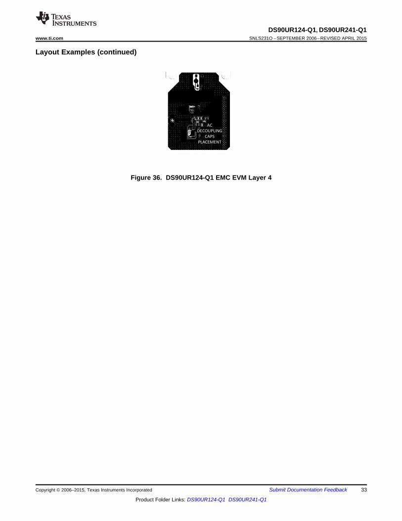
11.2 Layout Examples
Figure 33. Example DS90UR241-Q1 EMC Layout
Figure 34. DS90UR241-Q1 EMC EVM Layer 4
Figure 35. Example DS90UR124-Q1 EMC Layout
32 Submit Documentation Feedback Copyright © 2006–2015, Texas Instruments Incorporated
Product Folder Links: DS90UR124-Q1 DS90UR241-Q1
AC
DECOUPLING
CAPS
PLACEMENT
DS90UR124-Q1, DS90UR241-Q1www.ti.com SNLS231O –SEPTEMBER 2006–REVISED APRIL 2015
Layout Examples (continued)
Figure 36. DS90UR124-Q1 EMC EVM Layer 4
Copyright © 2006–2015, Texas Instruments Incorporated Submit Documentation Feedback 33
Product Folder Links: DS90UR124-Q1 DS90UR241-Q1
DS90UR124-Q1, DS90UR241-Q1SNLS231O –SEPTEMBER 2006–REVISED APRIL 2015 www.ti.com
12 Device and Documentation Support
12.1 Device Support
12.1.1 Third-Party Products DisclaimerTI'S PUBLICATION OF INFORMATION REGARDING THIRD-PARTY PRODUCTS OR SERVICES DOES NOTCONSTITUTE AN ENDORSEMENT REGARDING THE SUITABILITY OF SUCH PRODUCTS OR SERVICESOR A WARRANTY, REPRESENTATION OR ENDORSEMENT OF SUCH PRODUCTS OR SERVICES, EITHERALONE OR IN COMBINATION WITH ANY TI PRODUCT OR SERVICE.
12.2 Documentation Support
12.2.1 Related DocumentationFor related documentation see the following:• LVDS Interconnect Guidelines AN-1108, SNLA008• LVDS Interconnect Guidelines AN-905, SNLA035
12.3 Related LinksThe table below lists quick access links. Categories include technical documents, support and communityresources, tools and software, and quick access to sample or buy.
Table 5. Related LinksTECHNICAL TOOLS & SUPPORT &PARTS PRODUCT FOLDER SAMPLE & BUY DOCUMENTS SOFTWARE COMMUNITY
DS90UR124-Q1 Click here Click here Click here Click here Click hereDS90UR241-Q1 Click here Click here Click here Click here Click here
12.4 TrademarksAll trademarks are the property of their respective owners.
12.5 Electrostatic Discharge CautionThese devices have limited built-in ESD protection. The leads should be shorted together or the device placed in conductive foamduring storage or handling to prevent electrostatic damage to the MOS gates.
12.6 GlossarySLYZ022 — TI Glossary.
This glossary lists and explains terms, acronyms, and definitions.
13 Mechanical, Packaging, and Orderable InformationThe following pages include mechanical, packaging, and orderable information. This information is the mostcurrent data available for the designated devices. This data is subject to change without notice and revision ofthis document. For browser-based versions of this data sheet, refer to the left-hand navigation.
34 Submit Documentation Feedback Copyright © 2006–2015, Texas Instruments Incorporated
Product Folder Links: DS90UR124-Q1 DS90UR241-Q1

PACKAGE OPTION ADDENDUM
www.ti.com 28-Oct-2014
Addendum-Page 1
PACKAGING INFORMATION
Orderable Device Status(1)
Package Type PackageDrawing
Pins PackageQty
Eco Plan(2)
Lead/Ball Finish(6)
MSL Peak Temp(3)
Op Temp (°C) Device Marking(4/5)
Samples
DS90UR124IVS/NOPB ACTIVE TQFP PAG 64 160 Green (RoHS& no Sb/Br)
CU SN Level-3-260C-168 HR -40 to 105 DS90UR124IVS
DS90UR124IVSX/NOPB ACTIVE TQFP PAG 64 1000 Green (RoHS& no Sb/Br)
CU SN Level-3-260C-168 HR -40 to 105 DS90UR124IVS
DS90UR124QVS/NOPB ACTIVE TQFP PAG 64 160 Green (RoHS& no Sb/Br)
CU SN Level-3-260C-168 HR -40 to 105 DS90UR124QVS
DS90UR124QVSX/NOPB ACTIVE TQFP PAG 64 1000 Green (RoHS& no Sb/Br)
CU SN Level-3-260C-168 HR -40 to 105 DS90UR124QVS
DS90UR241IVS/NOPB ACTIVE TQFP PFB 48 250 Green (RoHS& no Sb/Br)
CU SN Level-3-260C-168 HR -40 to 105 DS90UR241IVS
DS90UR241IVSX/NOPB ACTIVE TQFP PFB 48 1000 Green (RoHS& no Sb/Br)
CU SN Level-3-260C-168 HR -40 to 105 DS90UR241IVS
DS90UR241QVS/NOPB ACTIVE TQFP PFB 48 250 Green (RoHS& no Sb/Br)
CU SN Level-3-260C-168 HR -40 to 105 DS90UR241QVS
DS90UR241QVSX/NOPB ACTIVE TQFP PFB 48 1000 Green (RoHS& no Sb/Br)
CU SN Level-3-260C-168 HR -40 to 105 DS90UR241QVS
(1) The marketing status values are defined as follows:ACTIVE: Product device recommended for new designs.LIFEBUY: TI has announced that the device will be discontinued, and a lifetime-buy period is in effect.NRND: Not recommended for new designs. Device is in production to support existing customers, but TI does not recommend using this part in a new design.PREVIEW: Device has been announced but is not in production. Samples may or may not be available.OBSOLETE: TI has discontinued the production of the device.
(2) Eco Plan - The planned eco-friendly classification: Pb-Free (RoHS), Pb-Free (RoHS Exempt), or Green (RoHS & no Sb/Br) - please check http://www.ti.com/productcontent for the latest availabilityinformation and additional product content details.TBD: The Pb-Free/Green conversion plan has not been defined.Pb-Free (RoHS): TI's terms "Lead-Free" or "Pb-Free" mean semiconductor products that are compatible with the current RoHS requirements for all 6 substances, including the requirement thatlead not exceed 0.1% by weight in homogeneous materials. Where designed to be soldered at high temperatures, TI Pb-Free products are suitable for use in specified lead-free processes.Pb-Free (RoHS Exempt): This component has a RoHS exemption for either 1) lead-based flip-chip solder bumps used between the die and package, or 2) lead-based die adhesive used betweenthe die and leadframe. The component is otherwise considered Pb-Free (RoHS compatible) as defined above.Green (RoHS & no Sb/Br): TI defines "Green" to mean Pb-Free (RoHS compatible), and free of Bromine (Br) and Antimony (Sb) based flame retardants (Br or Sb do not exceed 0.1% by weightin homogeneous material)
(3) MSL, Peak Temp. - The Moisture Sensitivity Level rating according to the JEDEC industry standard classifications, and peak solder temperature.

PACKAGE OPTION ADDENDUM
www.ti.com 28-Oct-2014
Addendum-Page 2
(4) There may be additional marking, which relates to the logo, the lot trace code information, or the environmental category on the device.
(5) Multiple Device Markings will be inside parentheses. Only one Device Marking contained in parentheses and separated by a "~" will appear on a device. If a line is indented then it is a continuationof the previous line and the two combined represent the entire Device Marking for that device.
(6) Lead/Ball Finish - Orderable Devices may have multiple material finish options. Finish options are separated by a vertical ruled line. Lead/Ball Finish values may wrap to two lines if the finishvalue exceeds the maximum column width.
Important Information and Disclaimer:The information provided on this page represents TI's knowledge and belief as of the date that it is provided. TI bases its knowledge and belief on informationprovided by third parties, and makes no representation or warranty as to the accuracy of such information. Efforts are underway to better integrate information from third parties. TI has taken andcontinues to take reasonable steps to provide representative and accurate information but may not have conducted destructive testing or chemical analysis on incoming materials and chemicals.TI and TI suppliers consider certain information to be proprietary, and thus CAS numbers and other limited information may not be available for release.
In no event shall TI's liability arising out of such information exceed the total purchase price of the TI part(s) at issue in this document sold by TI to Customer on an annual basis.
OTHER QUALIFIED VERSIONS OF DS90UR124, DS90UR124-Q1, DS90UR241, DS90UR241-Q1 :
• Catalog: DS90UR124, DS90UR241
• Automotive: DS90UR124-Q1, DS90UR241-Q1
NOTE: Qualified Version Definitions:
• Catalog - TI's standard catalog product
• Automotive - Q100 devices qualified for high-reliability automotive applications targeting zero defects

TAPE AND REEL INFORMATION
*All dimensions are nominal
Device PackageType
PackageDrawing
Pins SPQ ReelDiameter
(mm)
ReelWidth
W1 (mm)
A0(mm)
B0(mm)
K0(mm)
P1(mm)
W(mm)
Pin1Quadrant
DS90UR124IVSX/NOPB TQFP PAG 64 1000 330.0 24.4 13.0 13.0 1.45 16.0 24.0 Q2
DS90UR124QVSX/NOPB TQFP PAG 64 1000 330.0 24.4 13.0 13.0 1.45 16.0 24.0 Q2
DS90UR241IVSX/NOPB TQFP PFB 48 1000 330.0 16.4 9.3 9.3 2.2 12.0 16.0 Q2
DS90UR241QVSX/NOPB TQFP PFB 48 1000 330.0 16.4 9.3 9.3 2.2 12.0 16.0 Q2
PACKAGE MATERIALS INFORMATION
www.ti.com 28-Oct-2014
Pack Materials-Page 1

*All dimensions are nominal
Device Package Type Package Drawing Pins SPQ Length (mm) Width (mm) Height (mm)
DS90UR124IVSX/NOPB TQFP PAG 64 1000 367.0 367.0 45.0
DS90UR124QVSX/NOPB TQFP PAG 64 1000 367.0 367.0 45.0
DS90UR241IVSX/NOPB TQFP PFB 48 1000 367.0 367.0 38.0
DS90UR241QVSX/NOPB TQFP PFB 48 1000 367.0 367.0 38.0
PACKAGE MATERIALS INFORMATION
www.ti.com 28-Oct-2014
Pack Materials-Page 2

MECHANICAL DATA
MTQF006A – JANUARY 1995 – REVISED DECEMBER 1996
POST OFFICE BOX 655303 • DALLAS, TEXAS 75265
PAG (S-PQFP-G64) PLASTIC QUAD FLATPACK
0,13 NOM
0,25
0,450,75
Seating Plane
0,05 MIN
4040282/C 11/96
Gage Plane
33
0,170,27
16
48
1
7,50 TYP
49
64
SQ
9,80
1,050,95
11,8012,20
1,20 MAX
10,20SQ
17
32
0,08
0,50 M0,08
0°–7°
NOTES: A. All linear dimensions are in millimeters.B. This drawing is subject to change without notice.C. Falls within JEDEC MS-026

MECHANICAL DATA
MTQF019A – JANUARY 1995 – REVISED JANUARY 1998
POST OFFICE BOX 655303 • DALLAS, TEXAS 75265
PFB (S-PQFP-G48) PLASTIC QUAD FLATPACK
4073176/B 10/96
Gage Plane
0,13 NOM
0,25
0,450,75
Seating Plane
0,05 MIN
0,170,27
24
25
13
12
SQ
36
37
7,206,80
48
1
5,50 TYP
SQ8,809,20
1,050,95
1,20 MAX0,08
0,50 M0,08
0°–7°
NOTES: A. All linear dimensions are in millimeters.B. This drawing is subject to change without notice.C. Falls within JEDEC MS-026

IMPORTANT NOTICE
Texas Instruments Incorporated and its subsidiaries (TI) reserve the right to make corrections, enhancements, improvements and otherchanges to its semiconductor products and services per JESD46, latest issue, and to discontinue any product or service per JESD48, latestissue. Buyers should obtain the latest relevant information before placing orders and should verify that such information is current andcomplete. All semiconductor products (also referred to herein as “components”) are sold subject to TI’s terms and conditions of salesupplied at the time of order acknowledgment.TI warrants performance of its components to the specifications applicable at the time of sale, in accordance with the warranty in TI’s termsand conditions of sale of semiconductor products. Testing and other quality control techniques are used to the extent TI deems necessaryto support this warranty. Except where mandated by applicable law, testing of all parameters of each component is not necessarilyperformed.TI assumes no liability for applications assistance or the design of Buyers’ products. Buyers are responsible for their products andapplications using TI components. To minimize the risks associated with Buyers’ products and applications, Buyers should provideadequate design and operating safeguards.TI does not warrant or represent that any license, either express or implied, is granted under any patent right, copyright, mask work right, orother intellectual property right relating to any combination, machine, or process in which TI components or services are used. Informationpublished by TI regarding third-party products or services does not constitute a license to use such products or services or a warranty orendorsement thereof. Use of such information may require a license from a third party under the patents or other intellectual property of thethird party, or a license from TI under the patents or other intellectual property of TI.Reproduction of significant portions of TI information in TI data books or data sheets is permissible only if reproduction is without alterationand is accompanied by all associated warranties, conditions, limitations, and notices. TI is not responsible or liable for such altereddocumentation. Information of third parties may be subject to additional restrictions.Resale of TI components or services with statements different from or beyond the parameters stated by TI for that component or servicevoids all express and any implied warranties for the associated TI component or service and is an unfair and deceptive business practice.TI is not responsible or liable for any such statements.Buyer acknowledges and agrees that it is solely responsible for compliance with all legal, regulatory and safety-related requirementsconcerning its products, and any use of TI components in its applications, notwithstanding any applications-related information or supportthat may be provided by TI. Buyer represents and agrees that it has all the necessary expertise to create and implement safeguards whichanticipate dangerous consequences of failures, monitor failures and their consequences, lessen the likelihood of failures that might causeharm and take appropriate remedial actions. Buyer will fully indemnify TI and its representatives against any damages arising out of the useof any TI components in safety-critical applications.In some cases, TI components may be promoted specifically to facilitate safety-related applications. With such components, TI’s goal is tohelp enable customers to design and create their own end-product solutions that meet applicable functional safety standards andrequirements. Nonetheless, such components are subject to these terms.No TI components are authorized for use in FDA Class III (or similar life-critical medical equipment) unless authorized officers of the partieshave executed a special agreement specifically governing such use.Only those TI components which TI has specifically designated as military grade or “enhanced plastic” are designed and intended for use inmilitary/aerospace applications or environments. Buyer acknowledges and agrees that any military or aerospace use of TI componentswhich have not been so designated is solely at the Buyer's risk, and that Buyer is solely responsible for compliance with all legal andregulatory requirements in connection with such use.TI has specifically designated certain components as meeting ISO/TS16949 requirements, mainly for automotive use. In any case of use ofnon-designated products, TI will not be responsible for any failure to meet ISO/TS16949.
Products ApplicationsAudio www.ti.com/audio Automotive and Transportation www.ti.com/automotiveAmplifiers amplifier.ti.com Communications and Telecom www.ti.com/communicationsData Converters dataconverter.ti.com Computers and Peripherals www.ti.com/computersDLP® Products www.dlp.com Consumer Electronics www.ti.com/consumer-appsDSP dsp.ti.com Energy and Lighting www.ti.com/energyClocks and Timers www.ti.com/clocks Industrial www.ti.com/industrialInterface interface.ti.com Medical www.ti.com/medicalLogic logic.ti.com Security www.ti.com/securityPower Mgmt power.ti.com Space, Avionics and Defense www.ti.com/space-avionics-defenseMicrocontrollers microcontroller.ti.com Video and Imaging www.ti.com/videoRFID www.ti-rfid.comOMAP Applications Processors www.ti.com/omap TI E2E Community e2e.ti.comWireless Connectivity www.ti.com/wirelessconnectivity
Mailing Address: Texas Instruments, Post Office Box 655303, Dallas, Texas 75265Copyright © 2016, Texas Instruments Incorporated