Embed Size (px)
Citation preview
DSP, FPGA/ µ-Processor/
ECU
Deserializer
DS90UB913Q
Serializer
FPD-Link III
Bidirectional Control Channel
DS90UB914Q
Bidirectional Control Bus
Bidirectional Control Bus
Parallel Data In
Parallel Data Out10 or 12
2 2
Megapixel Imager/Sensor
10 or 12
GPO GPIO
4 4
2
HSYNC,VSYNC
2
HSYNC,VSYNC
Product
Folder
Sample &Buy
Technical
Documents
Tools &
Software
Support &Community
DS90UB913Q-Q1, DS90UB914Q-Q1SNLS420D –JULY 2012–REVISED JULY 2015
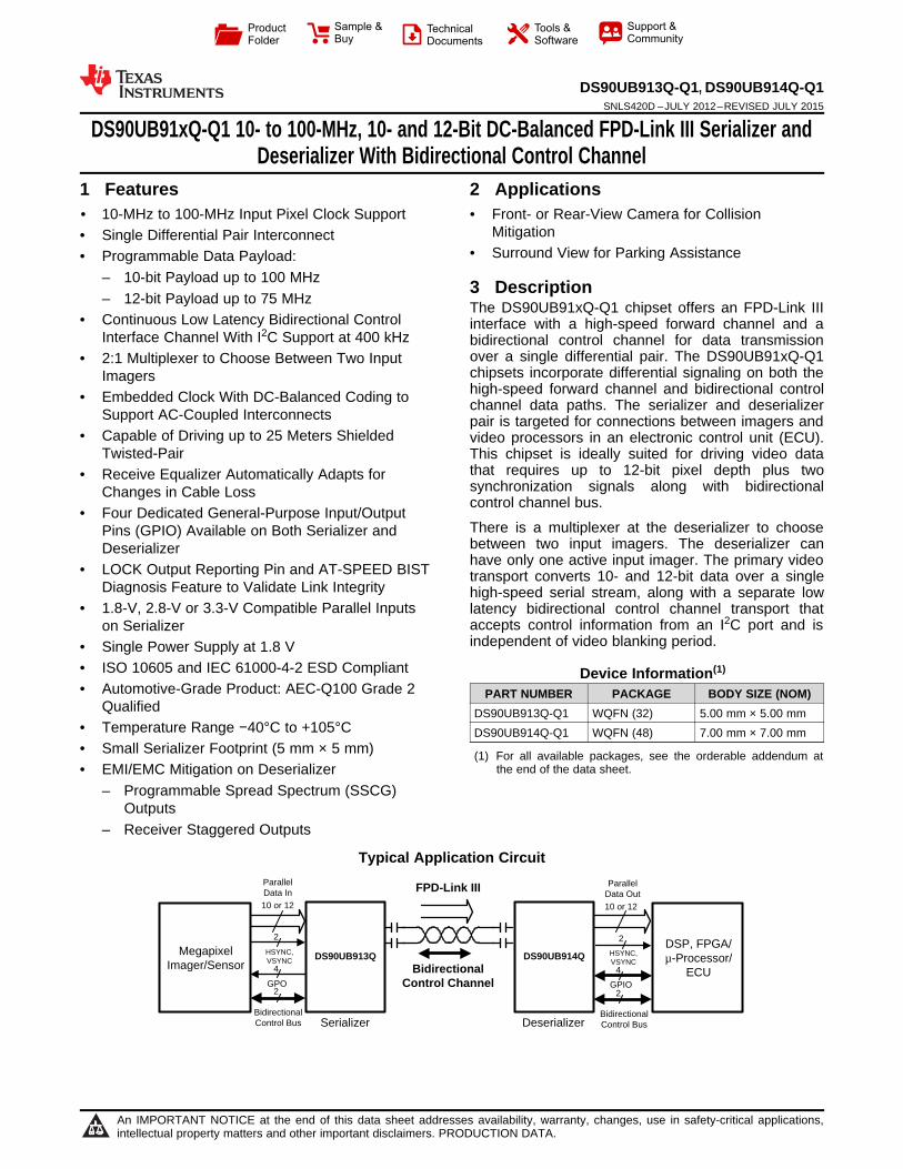
DS90UB91xQ-Q1 10- to 100-MHz, 10- and 12-Bit DC-Balanced FPD-Link III Serializer andDeserializer With Bidirectional Control Channel
1 Features 2 Applications1• 10-MHz to 100-MHz Input Pixel Clock Support • Front- or Rear-View Camera for Collision
Mitigation• Single Differential Pair Interconnect• Surround View for Parking Assistance• Programmable Data Payload:
– 10-bit Payload up to 100 MHz 3 Description– 12-bit Payload up to 75 MHz The DS90UB91xQ-Q1 chipset offers an FPD-Link III
• Continuous Low Latency Bidirectional Control interface with a high-speed forward channel and aInterface Channel With I2C Support at 400 kHz bidirectional control channel for data transmission
over a single differential pair. The DS90UB91xQ-Q1• 2:1 Multiplexer to Choose Between Two Inputchipsets incorporate differential signaling on both theImagershigh-speed forward channel and bidirectional control• Embedded Clock With DC-Balanced Coding to channel data paths. The serializer and deserializerSupport AC-Coupled Interconnects pair is targeted for connections between imagers and
• Capable of Driving up to 25 Meters Shielded video processors in an electronic control unit (ECU).Twisted-Pair This chipset is ideally suited for driving video data
that requires up to 12-bit pixel depth plus two• Receive Equalizer Automatically Adapts forsynchronization signals along with bidirectionalChanges in Cable Losscontrol channel bus.
• Four Dedicated General-Purpose Input/OutputThere is a multiplexer at the deserializer to choosePins (GPIO) Available on Both Serializer andbetween two input imagers. The deserializer canDeserializerhave only one active input imager. The primary video• LOCK Output Reporting Pin and AT-SPEED BIST transport converts 10- and 12-bit data over a single
Diagnosis Feature to Validate Link Integrity high-speed serial stream, along with a separate low• 1.8-V, 2.8-V or 3.3-V Compatible Parallel Inputs latency bidirectional control channel transport that
accepts control information from an I2C port and ison Serializerindependent of video blanking period.• Single Power Supply at 1.8 V
• ISO 10605 and IEC 61000-4-2 ESD Compliant Device Information(1)
• Automotive-Grade Product: AEC-Q100 Grade 2 PART NUMBER PACKAGE BODY SIZE (NOM)Qualified DS90UB913Q-Q1 WQFN (32) 5.00 mm × 5.00 mm
• Temperature Range −40°C to +105°C DS90UB914Q-Q1 WQFN (48) 7.00 mm × 7.00 mm• Small Serializer Footprint (5 mm × 5 mm) (1) For all available packages, see the orderable addendum at
the end of the data sheet.• EMI/EMC Mitigation on Deserializer– Programmable Spread Spectrum (SSCG)
Outputs– Receiver Staggered Outputs
Typical Application Circuit
1
An IMPORTANT NOTICE at the end of this data sheet addresses availability, warranty, changes, use in safety-critical applications,intellectual property matters and other important disclaimers. PRODUCTION DATA.

DS90UB913Q-Q1, DS90UB914Q-Q1SNLS420D –JULY 2012–REVISED JULY 2015 www.ti.com
Table of Contents9.1 AC Timing Diagrams and Test Circuits................... 201 Features .................................................................. 1
10 Detailed Description ........................................... 252 Applications ........................................................... 110.1 Overview ............................................................... 253 Description ............................................................. 110.2 Functional Block Diagram ..................................... 254 Revision History..................................................... 210.3 Feature Description............................................... 265 Description continued ........................................... 310.4 Device Functional Modes...................................... 336 Device Comparison Table ..................................... 310.5 Register Maps ....................................................... 417 Pin Configuration and Functions ......................... 4 11 Application and Implementation........................ 568 Specifications......................................................... 9 11.1 Applications Information........................................ 56
8.1 Absolute Maximum Ratings ...................................... 9 11.2 Typical Application ................................................ 568.2 ESD Ratings.............................................................. 9 12 Power Supply Recommendations ..................... 608.3 Recommended Operating Conditions....................... 9
13 Layout................................................................... 608.4 Thermal Information ................................................ 1013.1 Layout Guidelines ................................................. 608.5 Electrical Characteristics ........................................ 1013.2 Layout Example .................................................... 618.6 Timing Requirements: Recommended for Serializer
14 Device and Documentation Support ................. 63PCLK ....................................................................... 1414.1 Documentation Support ....................................... 638.7 AC Timing Specifications (SCL, SDA) - I2C
Compliant ................................................................. 15 14.2 Related Links ........................................................ 638.8 Bidirectional Control Bus DC Timing Specifications 14.3 Community Resources.......................................... 63
(SCL, SDA) - I2C Compliant..................................... 15 14.4 Trademarks ........................................................... 638.9 Switching Characteristics: Serializer....................... 16 14.5 Electrostatic Discharge Caution............................ 638.10 Switching Characteristics: Deserializer................. 17 14.6 Glossary ................................................................ 638.11 Typical Characteristics .......................................... 19 15 Mechanical, Packaging, and Orderable
9 Parameter Measurement Information ................ 20 Information ........................................................... 63
4 Revision HistoryNOTE: Page numbers for previous revisions may differ from page numbers in the current version.
Changes from Revision C (January 2014) to Revision D Page
• Added Pin Configuration and Functions section, ESD Ratings table, Feature Description section, Device FunctionalModes, Application and Implementation section, Power Supply Recommendations section, Layout section, Deviceand Documentation Support section, and Mechanical, Packaging, and Orderable Information section .............................. 1
• Updated datasheet to new TI layout....................................................................................................................................... 1• Added text and graphic to Power Up Requirements ........................................................................................................... 39
Changes from Revision B (April 2013) to Revision C Page
• Changed "PCLK from imager mode" value in DS90UB913Q Serializer MODE Resistor Value table from 0 kΩ to 100kΩ ......................................................................................................................................................................................... 35
• Changed Falling to Rising in RRFB...................................................................................................................................... 47• Changed Rising to Falling in RRFB...................................................................................................................................... 47
Changes from Revision A (April 2013) to Revision B Page
• Changed layout of National Data Sheet to TI format ........................................................................................................... 61
2 Submit Documentation Feedback Copyright © 2012–2015, Texas Instruments Incorporated
Product Folder Links: DS90UB913Q-Q1 DS90UB914Q-Q1

DS90UB913Q-Q1, DS90UB914Q-Q1www.ti.com SNLS420D –JULY 2012–REVISED JULY 2015
5 Description continuedUsing TI’s embedded-clock technology allows transparent full-duplex communication over a single differentialpair, carrying asymmetrical bidirectional control channel information in both directions. This single serial streamsimplifies transferring a wide data bus over PCB traces and cable by eliminating the skew problems betweenparallel data and clock paths. This significantly saves system cost by narrowing paths, which reduces PCBlayers, cable width, connector size and pins. In addition, the deserializer inputs provide adaptive equalization tocompensate for loss from the media over longer distances. Internal DC-balanced encoding and decoding is usedto support AC-coupled interconnects. The Serializer is offered in a 32-pin WQFN package and the deserializer isoffered in a 48-pin WQFN package.
6 Device Comparison Table
PART NUMBER FPD-III FUNCTION PACKAGE TRANSMISSION MEDIA PCLK FREQUENCYDS90UB913Q-Q1 Serializer 32-Pin RTV (WQFN) STP 10 to 100 MHzDS90UB913A-Q1 Serializer 32-Pin RTV (WQFN) Coax or STP 25 to 100 MHzDS90UB914Q-Q1 Deserializer 48-Pin RHS (WQFN) STP 10 to 100 MHzDS90UB914A-Q1 Deserializer 48-Pin RHS (WQFN) Coax or STP 25 to 100 MHz
Copyright © 2012–2015, Texas Instruments Incorporated Submit Documentation Feedback 3
Product Folder Links: DS90UB913Q-Q1 DS90UB914Q-Q1
3231
3029
2827
2625
1 2 3 4 5 6 7 8
910
1112
1314
1516
24 23 22 21 20 19 18 17
DS90UB913QSerializer
VDDIO
DIN[8]
DIN[9]
DIN[10]
DIN[11]
DIN[7]
DIN[6]D
IN[5
]
DIN
[4]
DIN
[3]
DIN
[2]
DIN
[1]
DIN
[0]
VDDCML
VDDT
VDDPLL
PDB
DOUT-
DOUT+
HS
YN
C
VS
YN
C
PC
LK
SC
L
SD
A
ID[x
]
RE
S
MO
DE
GP
O[2
]/ C
LKO
UT
GPO[1]
GPO[0]
VDDD
GP
O[3
]/ C
LKIN
DAP = GND
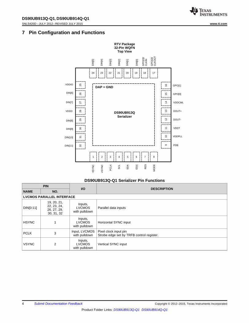
DS90UB913Q-Q1, DS90UB914Q-Q1SNLS420D –JULY 2012–REVISED JULY 2015 www.ti.com
7 Pin Configuration and Functions
RTV Package32-Pin WQFN
Top View
DS90UB913Q-Q1 Serializer Pin FunctionsPIN
I/O DESCRIPTIONNAME NO.LVCMOS PARALLEL INTERFACE
19, 20, 21, Inputs,22, 23, 24,DIN[0:11] LVCMOS Parallel data inputs26, 27, 29, with pulldown30, 31, 32Inputs,
HSYNC 1 LVCMOS Horizontal SYNC inputwith pulldown
Input, LVCMOS Pixel clock input pinPCLK 3 with pulldown Strobe edge set by TRFB control register.Inputs,
VSYNC 2 LVCMOS Vertical SYNC inputwith pulldown
4 Submit Documentation Feedback Copyright © 2012–2015, Texas Instruments Incorporated
Product Folder Links: DS90UB913Q-Q1 DS90UB914Q-Q1

DS90UB913Q-Q1, DS90UB914Q-Q1www.ti.com SNLS420D –JULY 2012–REVISED JULY 2015
DS90UB913Q-Q1 Serializer Pin Functions (continued)PIN
I/O DESCRIPTIONNAME NO.GENERAL-PURPOSE OUTPUT (GPO)
General-purpose output pins can be configured as outputs; used to control and respondOutput, to various commands. GPO[0:1] can be configured to be the outputs for input signalsGPO[1:0] 16, 15 LVCMOS coming from GPIO[0:1] pins on the deserializer or can be configured to be outputs of
the local register on the serializer.GPO2 pin can be configured to be the output for input signal coming from the GPIO2pin on the deserializer or can be configured to be the output of the local register on the
GPO[2]/ Output, serializer. It can also be configured to be the output clock pin when the DS90UB913Q-17CLKOUT LVCMOS Q1 device is used in the External Oscillator mode. See Applications Information for adetailed description of the DS90UB91xQ-Q1 chipsets working with the externaloscillator.GPO3 can be configured to be the output for input signals coming from the GPIO3 pinon the deserializer or can be configured to be the output of the local register setting on
GPO[3]/ Input/Output, the serializer. It can also be configured to be the input clock pin when the18CLKIN LVCMOS DS90UB913Q-Q1 serializer is working with an external oscillator. See ApplicationsInformation section for a detailed description of the DS90UB91xQ-Q1 chipsets workingwith an external oscillator.
BIDIRECTIONAL CONTROL BUS - I2C COMPATIBLEInput/Output, Clock line for the bidirectional control bus communicationSCL 4 Open-Drain SCL requires an external pullup resistor to VDDIO.Input/Output, Data line for the bidirectional control bus communicationSDA 5 Open-Drain SDA requires an external pullup resistor to VDDIO.
Device mode selectInput, LVCMOS Resistor to Ground and 10-kΩ pullup to 1.8-V rail. MODE pin on the serializer can beMODE 8 with pulldown used to select whether the system is running off the PCLK from the imager or an
external oscillator. See details in Table 3.Device ID address select
ID[x] 6 Input, analog The ID[x] pin on the serializer is used to assign the I2C device address. Resistor toGround and 10-kΩ pullup to 1.8-V rail. See Table 1.
CONTROL AND CONFIGURATIONPower down Mode Input PinPDB = H, serializer is enabled and is ON.Input, LVCMOSPDB 9 PDB = L, Serailizer is in power-down mode. When the serializer is in power-down, thewith pulldown PLL is shutdown, and IDD is minimized. Programmed control register data are NOTretained and reset to default values
Input, LVCMOS ReservedRES 7 with pulldown This pin MUST be tied LOW.FPD-Link III INTERFACE
Input/Output, Noninverting differential output, bidirectional control channel input. The interconnectDOUT+ 13 CML must be AC-coupled with a 100-nF capacitor.Input/Output, Inverting differential output, bidirectional control channel input. The interconnect must beDOUT– 12 CML AC-coupled with a 100-nF capacitor.
POWER AND GROUNDVDDPLL 10 Power, Analog PLL Power, 1.8 V ±5%VDDT 11 Power, Analog Tx Analog Power, 1.8 V ±5%VDDCML 14 Power, Analog CML and bidirectional channel driver power, 1.8 V ±5%VDDD 28 Power, Digital Digital power, 1.8 V ±5%
Power for I/O stage. The single-ended inputs and SDA, SCL are powered from VDDIO.VDDIO 25 Power, Digital VDDIO can be connected to a 1.8 V ±5% or 2.8 V ±10% or 3.3 V ±10%DAP must be grounded. DAP is the large metal contact at the bottom side, located at
VSS DAP Ground, DAP the center of the WQFN package. Connected to the ground plane (GND) with at least 9vias.
Copyright © 2012–2015, Texas Instruments Incorporated Submit Documentation Feedback 5
Product Folder Links: DS90UB913Q-Q1 DS90UB914Q-Q1

DS90UB914QDeserializer
1 2 3 4 5 6 7 8 9 10 11 12
13
14
15
16
17
18
19
20
21
22
23
24
36 35 34 33 32 31 30 29 28 27 26 25
48
47
46
45
44
43
42
41
40
39
38
37
RO
UT
[10]
RO
UT
[11]
VS
YN
C
PC
LK
OE
N
OS
S_S
EL
SC
L
SD
A
GP
IO[3
]
GP
IO[2
]
GP
IO[0
]
VD
DIO
1
RIN
1+
RIN
1-
IDx[
0]
VD
DR
VD
DS
SC
G
BIS
TE
N
VD
DIO
3
HS
YN
CG
PIO
[1]
VD
DC
ML1
IDx[
1]
ROUT[9]
ROUT[7]
ROUT[2]
ROUT[0]
ROUT[8]
ROUT[1]
ROUT[6]
VDDD
ROUT[5]
LOCK
PD
B
VDDPLL
RES
RES
RIN0-
RIN0+
VDDCML0
CMLOUTN
CMLOUTP
PASS
MODE
ROUT[4]
ROUT[3]
VDDIO2
DAP = GND
SEL
DS90UB913Q-Q1, DS90UB914Q-Q1SNLS420D –JULY 2012–REVISED JULY 2015 www.ti.com
RHS Package48-Pin WQFN
Top View
DS90UB914Q-Q1 Deserializer Pin FunctionsPIN
I/O DESCRIPTIONNAME NO.LVCMOS PARALLEL INTERFACE
11, 12, 13,14, 15, 16, Outputs,ROUT[11:0] Parallel data outputs18, 19, 21, LVCMOS22, 23, 24
Output,HSYNC 10 Horizontal SYNC outputLVCMOSOutput, Pixel clock output pinPCLK 8 LVCMOS Strobe edge set by RRFB control registerOutput,VSYNC 9 Vertical SYNC outputLVCMOS
GENERAL-PURPOSE INPUT/OUTPUT (GPIO)General-purpose input/output pins can be used to control and respond to variousDigital commands. They may be configured to be the input signals for the correspondingGPIO[1:0] 27, 28 Input/Output, GPOs on the serializer or they may be configured to be outputs to follow localLVCMOS register settings.General-purpose input/output pins GPO[2:3] can be configured to be input signals
Digital for GPOs on the serializer. In addition they can also be configured to be outputsGPIO[3:2] 25, 26 Input/Output to follow the local register settings. When the SerDes chipsets are working with
LVCMOS an external oscillator, these pins can be configured only to be outputs to followthe local register settings.
6 Submit Documentation Feedback Copyright © 2012–2015, Texas Instruments Incorporated
Product Folder Links: DS90UB913Q-Q1 DS90UB914Q-Q1

DS90UB913Q-Q1, DS90UB914Q-Q1www.ti.com SNLS420D –JULY 2012–REVISED JULY 2015
DS90UB914Q-Q1 Deserializer Pin Functions (continued)PIN
I/O DESCRIPTIONNAME NO.BIDIRECTIONAL CONTROL BUS - I2C COMPATIBLE
Input/Output, Clock line for the bidirectional control bus communicationSCL 2 Open-Drain SCL requires an external pullup resistor to VDDIO.Input/Output, Data line for bidirectional control bus communicationSDA 1 Open-Drain SDA requires an external pullup resistor to VDDIO.
Device mode select pinResistor-to-Ground and 10-kΩ pullup to 1.8-V rail. The MODE pin on thedeserializer can be used to configure the serializer and deserializer to work indifferent input PCLK range. See details in Table 8.12-bit low-frequency mode (10- to 50-MHz operation):In this mode, the serializer and deserializer can accept up to 12 bits DATA+2SYNC. Input PCLK range is from 10 MHz to 50 MHz.Input, LVCMOSMODE 37 12-bit high-frequency mode (15- to 75-MHz operation): In this mode, thewith pullup serializer and deserializer can accept up to 12 bits DATA + 2 SYNC. Input PCLKrange is from 15 MHz to 75 MHz.10-bit mode (20- to 100-MHz operation):In this mode, the serializer and deserializer can accept up to 10 bits DATA + 2SYNC. Input PCLK frequency can range from 20 MHz to 100 MHz.Refer to Table 4 in the Applications Information section on how to configure theMODE pin on the deserializer.The IDx[0] and IDx[1] pins on the deserializer are used to assign the I2C deviceaddress. Resistor-to-Ground and 10-kΩ pullup to 1.8-V rail. See Table 2
IDx[0:1] 35, 34 Input, analog Input pin to select the slave device address.Input is connect to external resistor divider to set programmable Device IDaddress.
CONTROL AND CONFIGURATIONPower-down mode input pinPDB = H, deserializer is enabled and is ON.Input, LVCMOSPDB 30 PDB = L, deserializer is in sleep (power-down mode). When the deserializer is inwith pulldown sleep, programmed control register data are NOT retained and reset to defaultvalues.LOCK status output pin
Output, LOCK = H, PLL is Locked, outputs are activeLOCK 48 LVCMOS LOCK = L, PLL is unlocked, ROUT and PCLK output states are controlled byOSS_SEL control register. May be used as link status.
Input BIST enable pinBISTEN 6 LVCMOS with BISTEN=H, BIST mode enabled
pulldown BISTEN=L, BIST mode is disabledPASS output pin for BIST mode.PASS = H, ERROR FREE transmissionOutput,PASS 47 PASS = L, one or more errors were detected in the received payload.LVCOMS See Built-In Self Test section for more information. Leave open if unused. Routeto test point (pad) recommended.
Input Output enable inputOEN 5 LVCMOS with Refer to Table 5pulldownInput Output sleep state select pinOSS_SEL 4 LVCMOS with Refer to Table 5pulldown
MUX select lineInput SEL = L, RIN0± input. This selects input A as the active channel on the
SEL 46 LVCMOS with deserializer.pulldown SEL = H, RIN1± input. This selects input B as the active channel on the
deserializer.
Copyright © 2012–2015, Texas Instruments Incorporated Submit Documentation Feedback 7
Product Folder Links: DS90UB913Q-Q1 DS90UB914Q-Q1

DS90UB913Q-Q1, DS90UB914Q-Q1SNLS420D –JULY 2012–REVISED JULY 2015 www.ti.com
DS90UB914Q-Q1 Deserializer Pin Functions (continued)PIN
I/O DESCRIPTIONNAME NO.FPD-LINK III INTERFACE
Input/Output, Noninverting differential input, bidirectional control channel. The IO must be ACRIN0+ 41 CML coupled with a 100-nF capacitorInput/Output, Inverting differential input, bidirectional control channel. The IO must be ACRIN0- 42 CML coupled with a 100-nF capacitorInput/Output, Noninverting differential input, bidirectional control channel. The IO must be ACRIN1+ 32 CML coupled with a 100-nF capacitorInput/Output, Inverting differential input, bidirectional control channel. The IO must be ACRIN1- 33 CML coupled with a 100-nF capacitor
RES 43, 44 — Reserved; This pin must always be tied low.CMLOUTP/N 38, 39 — Route to test point or leave open if unusedPOWER AND GROUND
LVCMOS I/O buffer power, The single-ended outputs and control input areVDDIO1/2/3 29, 20, 7 Power, Digital powered from VDDIO. VDDIO can be connected to a 1.8 V ±5% or 3.3 V ±10%VDDD 17 Power, Digital Digital core power, 1.8 V ±5%VDDSSCG 3 Power, Analog SSCG PLL power, 1.8 V ±5%VDDR 36 Power, Analog RX analog power, 1.8 V ±5%VDDCML0/1 40, 31 Power, Analog CML and bidirectional control channel drive power, 1.8 V±5%VDDPLL 45 Power, Analog PLL Power, 1.8 V ±5%
DAP must be grounded. DAP is the large metal contact at the bottom side,VSS DAP Ground, DAP located at the center of the WQFN package. Connected to the ground plane
(GND) with at least 16 vias.
8 Submit Documentation Feedback Copyright © 2012–2015, Texas Instruments Incorporated
Product Folder Links: DS90UB913Q-Q1 DS90UB914Q-Q1

DS90UB913Q-Q1, DS90UB914Q-Q1www.ti.com SNLS420D –JULY 2012–REVISED JULY 2015
8 Specifications
8.1 Absolute Maximum Ratingsover operating free-air temperature range (unless otherwise noted) (1) (2) (3)
MIN MAX UNITSupply voltage – VDDn (1.8 V) −0.3 2.5 VSupply voltage – VDDIO −0.3 4.0 VLVCMOS input voltage −0.3 VDDIO + 0.3 VCML driver I/O voltage (VDD) −0.3 VDD + 0.3 VCML receiver I/O voltage (VDD) −0.3 VDD + 0.3 VJunction temperature 150 °C
1/θJA aboveMaximum package power dissipation capacity package °C/W+25°Air discharge (DOUT+, DOUT–, RIN+, RIN–) −25 25 kVContact discharge (DOUT+, DOUT–, RIN+, RIN–) −7 7 kVStorage temperature Tstg −65 150 °C
(1) Stresses beyond those listed under Absolute Maximum Ratings may cause permanent damage to the device. These are stress ratingsonly, which do not imply functional operation of the device at these or any other conditions beyond those indicated under RecommendedOperating Conditions. Exposure to absolute-maximum-rated conditions for extended periods may affect device reliability.
(2) If Military/Aerospace specified devices are required, contact the Texas Instruments Sales Office/ Distributors for availability andspecifications.
(3) For soldering specifications: see product folder at www.ti.com and SNOA549.
8.2 ESD RatingsVALUE UNIT
Human body model (HBM), per AEC Q100-002 (1) ±8000Charged-device model (CDM), per AEC Q100-011 ±1000Machine model (MM) ±250
ElectrostaticV(ESD) Air Discharge (DOUT+, DOUT-, RIN+, RIN-) ≥±25 000 Vdischarge IEC 61000-4-2 (2)Contact Discharge (DOUT+, DOUT-, RIN+, RIN-) ≥±7000Air Discharge ≥±15 000
ISO10605 (3) (4)Contact Discharge ≥±8000
(1) AEC Q100-002 indicates HBM stressing is done in accordance with the ANSI/ESDA/JEDEC JS-001 specification.(2) RD = 330 Ω, CS = 150 pF(3) RD = 330 Ω, CS = 150 / 330 pF(4) RD = 2 KΩ, CS = 150 / 330 pF
8.3 Recommended Operating Conditionsover operating free-air temperature range (unless otherwise noted)
MIN NOM MAX UNITSupply voltage (VDDn) 1.71 1.8 1.89 VLVCMOS supply voltage (VDDIO) OR 1.71 1.8 1.89LVCMOS supply voltage (VDDIO) OR 3.0 3.3 3.6 VLVCMOS supply voltage (VDDIO) only serializer 2.52 2.8 3.08
VDDn (1.8 V) 25Supply noise (1) VDDIO (1.8 V) 25 mVp-p
VDDIO (3.3 V) 50Operating free-air temperature (TA) –40 25 105 °CPCLK clock frequency 10 100 MHz
(1) Supply noise testing was done with minimum capacitors (as shown on Figure 49 and Figure 48) on the PCB. A sinusoidal signal is ACcoupled to the VDDn (1.8-V) supply with amplitude = 25 mVp-p measured at the device VDDn pins. Bit error rate testing of input to theserializer and output of the deserializer with 10 meter cable shows no error when the noise frequency on the serializer is less than1 MHz. The deserializer on the other hand shows no error when the noise frequency is less than 750 kHz.
Copyright © 2012–2015, Texas Instruments Incorporated Submit Documentation Feedback 9
Product Folder Links: DS90UB913Q-Q1 DS90UB914Q-Q1

DS90UB913Q-Q1, DS90UB914Q-Q1SNLS420D –JULY 2012–REVISED JULY 2015 www.ti.com
8.4 Thermal InformationDS90UB913Q-Q1 DS90UB914Q-Q1
THERMAL METRIC (1) RTV (WQFN) RHS (WQFN) UNIT32 PINS 48 PINS
RθJA Junction-to-ambient thermal resistance 38.4 26.9 °C/WRθJC(top) Junction-to-case (top) thermal resistance 6.9 4.4 °C/W
(1) For more information about traditional and new thermal metrics, see the Semiconductor and IC Package Thermal Metrics applicationreport, SPRA953.
8.5 Electrical Characteristicsover recommended operating supply and temperature ranges unless otherwise specified. (1) (2) (3)
PARAMETER TEST CONDITIONS MIN TYP MAX UNITLVCMOS DC SPECIFICATIONS 3.3V I/O (SERIALIZER INPUTS, DESERIALIZER OUTPUTS, GPI, GPO, CONTROL INPUTS ANDOUTPUTS)
High level inputVIH VIN = 3 V to 3.6 V 2 VIN VvoltageLow level inputVIL VIN = 3 V to 3.6 V GND 0.8 Vvoltage
IIN Input current VIN = 0 V or 3.6 V, VIN = 3 V to 3.6 V −20 ±1 20 µAHigh level outputVOH VDDIO = 3 V to 3.6 V, IOH = −4 mA 2.4 VDDIO VvoltageLow level outputVOL VDDIO = 3 V to 3.6 V, IOL = +4 mA GND 0.4 Vvoltage
Serializer –15GPO outputsOutput short circuitIOS VOUT = 0 V mAcurrent Deserializer LVCMOS –35outputsTRI-STATE output PDB = 0 V,IOZ LVCMOS outputs –20 20 µAcurrent VOUT = 0 V or VDD
LVCMOS DC SPECIFICATIONS 1.8V I/O (SERIALIZER INPUTS, DESERIALIZER OUTPUTS, GPI, GPO, CONTROL INPUTS ANDOUTPUTS)
High level inputVIH VIN = 1.71 V to 1.89 V 0.65 VIN VINvoltageV
Low level inputVIL VIN = 1.71 V to 1.89 V GND 0.35 VINvoltageIIN Input current VIN = 0 V or 1.89 V, VIN = 1.71 V to 1.89 V –20 ±1 20 µA
High level output VDDIO –VOH VDDIO = 1.71 V to 1.89 V, IOH = −4 mA VDDIO Vvoltage 0.45VDDIO = 1.71 V to 1.89Low level output Deserializer LVCMOSVOL V GND 0.45 Vvoltage outputsIOL = 4 mA
Serializer –11GPO outputsOutput short circuitIOS VOUT = 0 V mAcurrent Deserializer LVCMOS –17outputsTRI-STATE output PDB = 0 V,IOZ LVCMOS outputs –20 20 µAcurrent VOUT = 0 V or VDD
(1) The Electrical Characteristics tables list ensured specifications under the listed Recommended Operating Conditions except asotherwise modified or specified by the Electrical Characteristics Conditions and/or Notes. Typical specifications are estimations only andare not ensured.
(2) Current into device pins is defined as positive. Current out of a device pin is defined as negative. Voltages are referenced to groundexcept VOD, ΔVOD, VTH and VTL which are differential voltages.
(3) Typical values represent most likely parametric norms at 1.8 V or 3.3 V, TA = 25°C, and at the Recommended Operation Conditions atthe time of product characterization and are not specified.
10 Submit Documentation Feedback Copyright © 2012–2015, Texas Instruments Incorporated
Product Folder Links: DS90UB913Q-Q1 DS90UB914Q-Q1

DS90UB913Q-Q1, DS90UB914Q-Q1www.ti.com SNLS420D –JULY 2012–REVISED JULY 2015
Electrical Characteristics (continued)over recommended operating supply and temperature ranges unless otherwise specified.(1) (2) (3)
PARAMETER TEST CONDITIONS MIN TYP MAX UNITLVCMOS DC SPECIFICATIONS 2.8-V I/O (SERIALIZER INPUTS, GPI, GPO, CONTROL INPUTS AND OUTPUTS)
High level inputVIH VIN = 2.52 V to 3.08 V 0.7 VIN VINvoltageV
Low level inputVIL VIN = 2.52 V to 3.08 V GND 0.3 VINvoltageIIN Input current VIN = 0 V or 3.08 V, VIN = 2.52 V to 3.08 V −20 ±1 20 µA
High level outputVOH VDDIO = 2.52 V to 3.08 V, IOH = −4 mA VDDIO – 0.4 VDDIO VvoltageVDDIO =2.52 V to 3.08Low level output Deserializer LVCMOSVOL V GND 0.4 Vvoltage outputsIOL = 4 mA
Serializer −11GPO outputsOutput short circuitIOS VOUT = 0 V mAcurrent Deserializer LVCMOS −20outputsTRI-STATE output PDB = 0 V,IOZ LVCMOS outputs −20 20 µAcurrent VOUT = 0 V or VDD
CML DRIVER DC SPECIFICATIONS (DOUT+, DOUT–)Output differential|VOD| RL = 100 Ω (see Figure 9) 268 340 412 mVvoltageOutput differentialΔVOD RL = 100 Ω 1 50 mVvoltage unbalanceOutput differentialVOS RL = 100 Ω (see Figure 9) VDD – VOD/2 Voffset voltageOffset voltageΔVOS RL = 100 Ω 1 50 mVunbalanceOutput shortIOS DOUT± = 0 V –26 mAcircuit currentDifferential internal
RT termination Differential across DOUT+ and DOUT– 80 100 120 Ωresistance
CML RECEIVER DC SPECIFICATIONS (RIN0+, RIN0–, RIN1+, RIN1– )IIN Input current VIN = VDD or 0 V, VDD = 1.89 V −20 1 20 µA
Differential internalRT termination Differential across RIN+ and RIN- 80 100 120 Ω
resistanceCML RECEIVER AC SPECIFICATIONS (RIN0+, RIN0–, RIN1+, RIN1– )
Minimum allowable|Vswing| swing for 1010 Line rate = 1.4 Gbps (see Figure 11) 135 mV
pattern (4)
CML MONITOR OUTPUT DRIVER SPECIFICATIONS (CMLOUTP, CMLOUTN)Differential outputEw 0.45 UIeye opening RL = 100 Ω
Jitter frequency > f / 40 (see Figure 20)Differential outputEH 200 mVeye height
(4) Specification is ensured by characterization and is not tested in production.
Copyright © 2012–2015, Texas Instruments Incorporated Submit Documentation Feedback 11
Product Folder Links: DS90UB913Q-Q1 DS90UB914Q-Q1

DS90UB913Q-Q1, DS90UB914Q-Q1SNLS420D –JULY 2012–REVISED JULY 2015 www.ti.com
Electrical Characteristics (continued)over recommended operating supply and temperature ranges unless otherwise specified.(1) (2) (3)
PARAMETER TEST CONDITIONS MIN TYP MAX UNITSERIALIZER AND DESERIALIZER SUPPLY CURRENT *DIGITAL, PLL, AND ANALOG VDD
VDDn = 1.89 VVDDIO = 3.6 Vf = 100 MHz, 61 80 mA10-bit modedefault registersVDDn = 1.89 VVDDIO = 3.6 V
RL = 100 Ω f = 75 MHz, 61 80WORST CASE pattern 12-bit high-frequency(see Figure 6) mode
default registersmA
VDDn = 1.89 VVDDIO = 3.6 Vf = 50 MHz, 61 8012-bit low-frequencymodeSerializer (TX)default registersVDDn supply currentIDDT (includes load VDDn = 1.89 V
current) VDDIO = 3.6 Vf = 100 MHz, 5410-bit modedefault registersVDDn = 1.89 VVDDIO = 3.6 V
RL = 100 Ω f = 75 MHz, 54RANDOM PRBS-7 12-bit high-frequency mApattern mode
default registersVDD = 1.89 VVDDIO = 3.6 Vf = 50 MHz, 5412-bit low-frequencymodedefault registersVDDIO = 1.89 Vf = 75 MHz, 1.5 312-bit high-freq modeSerializer (TX) RL = 100 Ω default registersVDDIO supplyIDDIOT WORST CASE pattern mAcurrent (includes VDDIO = 3.6 V(see Figure 6)load current) f = 75 MHz, 5 812-bit high-frequencymode default registersVDDIO = 1.89 V 300 900 µASerializer (TX) Default registersPDB = 0 V; all otherIDDTZ supply current LVCMOS inputs = 0 V VDDIO = 3.6 Vpower-down 300 900 µADefault registersVDDIO = 1.89 V 15 100 µASerializer (TX) Default registersPDB = 0 V; All otherIDDIOTZ VDDIO supply LVCMOS Inputs = 0 V VDDIO = 3.6 Vcurrent power-down 15 100 µADefault registers
12 Submit Documentation Feedback Copyright © 2012–2015, Texas Instruments Incorporated
Product Folder Links: DS90UB913Q-Q1 DS90UB914Q-Q1

DS90UB913Q-Q1, DS90UB914Q-Q1www.ti.com SNLS420D –JULY 2012–REVISED JULY 2015
Electrical Characteristics (continued)over recommended operating supply and temperature ranges unless otherwise specified.(1) (2) (3)
PARAMETER TEST CONDITIONS MIN TYP MAX UNITf = 100 MHz, 10-bit 22 42mode
VDDIO = 1.89 V f = 75 MHz, 12-bit high-CL = 8 pF 19 39 mAfreq modeWORST CASE patternf = 50 MHz, 12-bit low- 21 32freq modef = 100 MHz, 10–bit 15mode
VDDIO = 1.89 V f = 75 MHz, 12-bit high-CL=8pF 12 mAfreq modeRandom patternf = 50 MHz, 12-bit low- 14freq modef = 100 MHz, 10-bit 42 55mode
VDDIO = 3.6 V f = 75 MHz, 12-bit high-CL = 8 pF 37 50 mAfreq modeWORST CASE patternf = 50 MHz, 12-bit low- 25 38freq modef = 100 MHz, 10-bit 35mode
VDDIO = 3.6 V f = 75 MHz, 12-bit high-CL = 8 pF 30 mAfreq modeRandom patternf = 50 MHz, 12-bit low-Deserializer (RX) 18freq modetotal supply currentIDDIOR (includes load f = 100 MHz, 10-bit 15current) mode
VDDIO = 1.89 V f = 75 MHz, 12-bit high-CL = 4 pF 11 mAfreq modeWORST CASE patternf = 50 MHz, 12-bit low- 16freq modef = 100 MHz, 10-bit 8mode
VDDIO = 1.89 V f = 75 MHz, 12-bit high-CL = 4 pF 4 mAfreq modeRandom patternf = 50 MHz, 12-bit low- 9freq modef = 100 MHz, 10-bit 36mode
VDDIO = 3.6 V f = 75 MHz, 12-bit high-CL = 4 pF 29 mAfreq modeWORST CASE patternf = 50 MHz, 12-bit low- 20freq modef = 100 MHz, 10-bit 29mode
VDDIO = 3.6 V f = 75 MHz, 12-bit high-CL = 4 pF 22 mAfreq modeRandom patternf = 50 MHz, 12-bit low- 13freq mode
Copyright © 2012–2015, Texas Instruments Incorporated Submit Documentation Feedback 13
Product Folder Links: DS90UB913Q-Q1 DS90UB914Q-Q1

DS90UB913Q-Q1, DS90UB914Q-Q1SNLS420D –JULY 2012–REVISED JULY 2015 www.ti.com
Electrical Characteristics (continued)over recommended operating supply and temperature ranges unless otherwise specified.(1) (2) (3)
PARAMETER TEST CONDITIONS MIN TYP MAX UNITf = 100 MHz, 64 11010-bit modef = 75 MHz,VDDn = 1.89 V 12-bit high-frequency 67 114CL = 4 pF modeWORST CASE patternf = 50 MHz,Deserializer (RX)12-bit low-frequency 63 96VDDn supply currentIDDR mAmode(includes load
current) f = 100 MHz, 5710-bit modeVDDn = 1.89 V f = 75 MHz, 12–bitCL = 4 pF 60high-frequency modeRandom pattern
f = 50 MHz, 12-bit 56low-frequency modePBB = 0 V, all other VDDIO = 1.89 V 42 400Deserializer (RX) LVCMOS Inputs=0 V Default registers
IDDRZ supply current µAPBB = 0 V, all other VDDIO = 3.6 Vpower-down 42 400LVCMOS Inputs=0 V Default registers
Deserializer (RX) VDDIO = 1.89 V 8 40PDB = 0 V, all otherIDDIORZ VDD supply current µALVCMOS Inputs = 0 V VDDIO = 3.6 V 360 800power-down
8.6 Timing Requirements: Recommended for Serializer PCLKover recommended operating supply and temperature ranges unless otherwise specified. (1)
TEST CONDITIONS PIN/FREQ MIN NOM MAX UNIT10-bit mode 10 T 5012-bit high-frequency 13.33 T 66.66tTCP Transmit clock period mode ns12-bit low-frequency 20 T 100mode
Transmit clocktTCIH 0.4T 0.5T 0.6T nsinput high timeTransmit clocktTCIL 0.4T 0.5T 0.6T nsinput low time
20 MHz–100 MHz, 0.5T 2.5T 0.3T10-bit modePCLK input transition 15 MHz to 75 MHz, 12-bittCLKT 0.5T 2.5T 0.3T nstime (Figure 12) high-frequency mode
10 MHz to 50 MHz, 12-bit 0.5T 2.5T 0.3Tlow-frequency modePCLK input jitter
tJIT0 (PCLK from imager Refer to jitter freq > f / 40 f = 10 to 100 MHz 0.1T nsmode)PCLK input jitter (externaltJIT1 Refer to jitter freq > f / 40 f = 10 to 100 MHz 1T nsoscillator mode)
tJIT2 External oscillator jitter 0.1 UI
(1) Recommended input timing requirements are input specifications and not tested in production.
14 Submit Documentation Feedback Copyright © 2012–2015, Texas Instruments Incorporated
Product Folder Links: DS90UB913Q-Q1 DS90UB914Q-Q1

DS90UB913Q-Q1, DS90UB914Q-Q1www.ti.com SNLS420D –JULY 2012–REVISED JULY 2015
8.7 AC Timing Specifications (SCL, SDA) - I2C Compliantover recommended supply and temperature ranges unless otherwise specified. (See Figure 5)
TEST CONDITIONS MIN NOM MAX UNITRECOMMENDED INPUT TIMING REQUIREMENTS
Standard mode >0 100fSCL SCL clock frequency kHz
Fast mode >0 400Standard mode 4.7
tLOW SCL low period µsFast mode 1.3Standard mode 4.0
tHIGH SCL high period µsFast mode 0.6Standard mode 4Hold time for a start or atHD:STA µsrepeated start condition Fast mode 0.6Standard mode 4.7Setup time for a start or atSU:STA µsrepeated start condition Fast mode 0.6Standard mode 0 3.45
tHD:DAT Data hold time µsFast mode 0 900Standard mode 250
tSU:DAT Data setup time nsFast mode 100Standard mode 4Setup time for STOPtSU:STO µscondition Fast mode 0.6Standard mode 4.7Bus free time betweentBUF µsstop and start Fast mode 1.3Standard mode 1000
tr SCL and SDA rise time nsFast mode 300Standard mode 300
tf SCL and SDA fall time nsFast mode 300
8.8 Bidirectional Control Bus DC Timing Specifications (SCL, SDA) - I2C Compliantover recommended supply and temperature ranges unless otherwise specified (1)
TEST CONDITIONS MIN NOM MAX UNITRECOMMENDED INPUT TIMING REQUIREMENTSVIH Input high level SDA and SCL 0.7 × VDDIO VDDIO VVIL Input low level SDA and SCL GND 0.3 × VDDIO VVHY Input hysteresis >50 mVVOL Output low level SDA, IOL = 0.5 mA 0 0.4 VIIN Input current SDA or SCL, VIN = VDDOP OR GND −10 10 µAtR SDA rise time-READ 430 nsSDA, RPU = 10 kΩ, Cb ≤ 400 pF (see
Figure 5)tF SDA fall time-READ 20 nstSU;DAT See Figure 5 560 nstHD;DAT See Figure 5 615 nstSP 50 nsCIN SDA or SCL <5 pF
(1) Specification is ensured by design.
Copyright © 2012–2015, Texas Instruments Incorporated Submit Documentation Feedback 15
Product Folder Links: DS90UB913Q-Q1 DS90UB914Q-Q1

DS90UB913Q-Q1, DS90UB914Q-Q1SNLS420D –JULY 2012–REVISED JULY 2015 www.ti.com
8.9 Switching Characteristics: Serializerover recommended operating supply and temperature ranges unless otherwise specified.
PARAMETER TEST CONDITIONS MIN TYP MAX UNITCML low-to-high transitiontLHT RL = 100 Ω (see Figure 7) 150 330 pstimeCML high-to-low transitiontHLT RL = 100 Ω (see Figure 7) 150 330 pstime
tDIS Data input setup to PCLK 2 nsSerializer data inputs (see Figure 13)Data input hold fromtDIH 2 nsPCLK
tPLD Serializer PLL lock time RL = 100 Ω (1) (2), (see Figure 14) 1 2 msRT = 100 Ω, 10-bit modeRegister 0x03h b[0] (TRFB = 1) (see 32.5T 38T 44TFigure 15)
tSD Serializer delay (2) nsRT = 100 Ω, 12-bit modeRegister 0x03h b[0] (TRFB = 1) (see 11.75T 13T 15TFigure 15)Serializer output intrinsic deterministic jitter.Serializer outputtJIND Measured (cycle-cycle) with PRBS-7 test 0.13 UIdeterministic jitter pattern (3) (4)
Serializer output Serializer output intrinsic random jitter (cycle-tJINR 0.04 UIrandom jitter cycle). Alternating-1,0 pattern. (3) (4)
Serializer output peak-to-peak jitter includesPeak-to-peak serializer deterministic jitter, random jitter, and jittertJINT 0.396 UIoutput jitter transfer from serializer input. Measured
(cycle-cycle) with PRBS-7 test pattern. (3) (4)
PCLK = 100 MHz 2.210-bit mode. Default registersSerializer jitter PCLK = 75 MHzλSTXBW transfer function –3-dB 2.2 MHz12-bit high-frequency mode. Default registersbandwidth (5)
PCLK = 50 MHz 2.212-bit low-frequency mode. Default registersPCLK = 100 MHz 1.0610-bit mode. Default Registers
Serializer jitter PCLK = 75 MHzδSTX transfer function 1.09 dB12-bit high-frequency mode. Default registers(peaking) (5)
PCLK = 50 MHz 1.1612-bit low-frequency mode. Default registersPCLK = 100 MHz 40010-bit mode. Default registers
Serializer jitter PCLK = 75 MHzδSTXf transfer function 500 kHz12-bit high-frequency mode. Default registers(peaking frequency) (5)
PCLK = 50 MHz 60012-bit low-frequency mode. Default registers
(1) tPLD and tDDLT is the time required by the serializer and deserializer to obtain lock when exiting power-down state with an active PCLK(2) Specification is ensured by design.(3) Typical values represent most likely parametric norms at 1.8 V or 3.3 V, TA = 25°C, and at the recommended operation conditions at the
time of product characterization and are not specified.(4) UI – Unit Interval is equivalent to one ideal serialized data bit width. The UI scales with PCLK frequency.(5) Specification is ensured by characterization and is not tested in production.
16 Submit Documentation Feedback Copyright © 2012–2015, Texas Instruments Incorporated
Product Folder Links: DS90UB913Q-Q1 DS90UB914Q-Q1
DS90UB913Q-Q1, DS90UB914Q-Q1www.ti.com SNLS420D –JULY 2012–REVISED JULY 2015
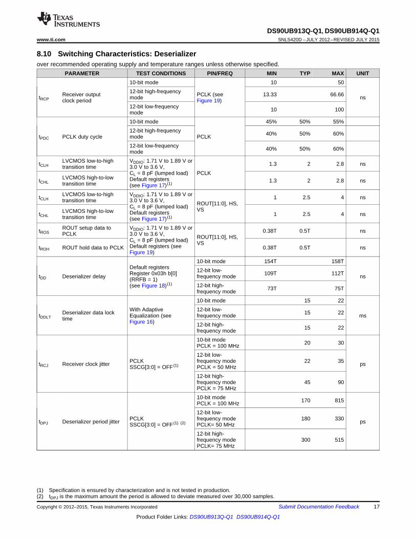
8.10 Switching Characteristics: Deserializerover recommended operating supply and temperature ranges unless otherwise specified.
PARAMETER TEST CONDITIONS PIN/FREQ MIN TYP MAX UNIT10-bit mode 10 5012-bit high-frequencyReceiver output PCLK (see 13.33 66.66tRCP mode nsclock period Figure 19)12-bit low-frequency 10 100mode10-bit mode 45% 50% 55%12-bit high-frequency 40% 50% 60%tPDC PCLK duty cycle mode PCLK12-bit low-frequency 40% 50% 60%mode
LVCMOS low-to-high VDDIO: 1.71 V to 1.89 V ortCLH 1.3 2 2.8 nstransition time 3.0 V to 3.6 V,CL = 8 pF (lumped load) PCLK
LVCMOS high-to-low Default registerstCHL 1.3 2 2.8 nstransition time (see Figure 17) (1)
LVCMOS low-to-high VDDIO: 1.71 V to 1.89 V ortCLH 1 2.5 4 nstransition time 3.0 V to 3.6 V, ROUT[11:0], HS,CL = 8 pF (lumped load) VSLVCMOS high-to-low Default registerstCHL 1 2.5 4 nstransition time (see Figure 17) (1)
ROUT setup data to VDDIO: 1.71 V to 1.89 V ortROS 0.38T 0.5T nsPCLK 3.0 V to 3.6 V, ROUT[11:0], HS,CL = 8 pF (lumped load) VSDefault registers (seetROH ROUT hold data to PCLK 0.38T 0.5T nsFigure 19)
10-bit mode 154T 158TDefault registers 12-bit low-Register 0x03h b[0] 109T 112TtDD Deserializer delay frequency mode ns(RRFB = 1)
12-bit high-(see Figure 18) (1)73T 75Tfrequency mode
10-bit mode 15 22With Adaptive 12-bit low-Deserializer data lock 15 22tDDLT Equalization (see frequency mode mstime Figure 16) 12-bit high- 15 22frequency mode
10-bit mode 20 30PCLK = 100 MHz12-bit low-
PCLK frequency mode 22 35tRCJ Receiver clock jitter psSSCG[3:0] = OFF (1) PCLK = 50 MHz12-bit high-frequency mode 45 90PCLK = 75 MHz10-bit mode 170 815PCLK = 100 MHz12-bit low-
PCLK frequency mode 180 330tDPJ Deserializer period jitter psSSCG[3:0] = OFF (1) (2) PCLK= 50 MHz12-bit high-frequency mode 300 515PCLK= 75 MHz
(1) Specification is ensured by characterization and is not tested in production.(2) tDPJ is the maximum amount the period is allowed to deviate measured over 30,000 samples.
Copyright © 2012–2015, Texas Instruments Incorporated Submit Documentation Feedback 17
Product Folder Links: DS90UB913Q-Q1 DS90UB914Q-Q1
DS90UB913Q-Q1, DS90UB914Q-Q1SNLS420D –JULY 2012–REVISED JULY 2015 www.ti.com
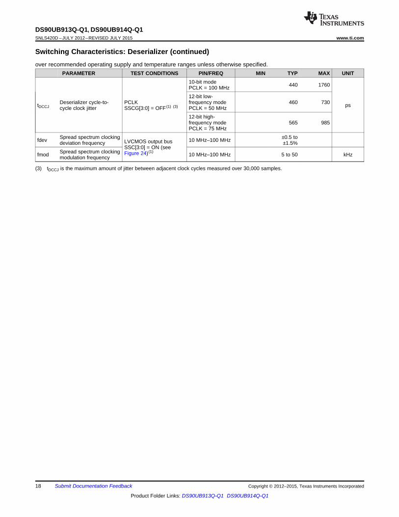
Switching Characteristics: Deserializer (continued)over recommended operating supply and temperature ranges unless otherwise specified.
PARAMETER TEST CONDITIONS PIN/FREQ MIN TYP MAX UNIT10-bit mode 440 1760PCLK = 100 MHz12-bit low-
Deserializer cycle-to- PCLK frequency mode 460 730tDCCJ pscycle clock jitter SSCG[3:0] = OFF (1) (3) PCLK = 50 MHz12-bit high-frequency mode 565 985PCLK = 75 MHz
Spread spectrum clocking ±0.5 tofdev 10 MHz–100 MHzLVCMOS output busdeviation frequency ±1.5%SSC[3:0] = ON (see
Spread spectrum clocking Figure 24) (1)fmod 10 MHz–100 MHz 5 to 50 kHzmodulation frequency
(3) tDCCJ is the maximum amount of jitter between adjacent clock cycles measured over 30,000 samples.
18 Submit Documentation Feedback Copyright © 2012–2015, Texas Instruments Incorporated
Product Folder Links: DS90UB913Q-Q1 DS90UB914Q-Q1

600
SERIAL LINE FREQUENCY (MHz)
0
2
4
6
8
10
12
14
16
18
EQ
UA
LIZ
ER
GA
IN (
dB)
700500400300200100
200 300 400 500 600 700
SERIAL LINE FREQUENCY (MHz)
0
5
10
15
20
25
EF
FE
CT
IVE
GA
IN (
dB)
100
VOD-Vswing Loss
914 Equalizer Gain (dB)
Allowable InterconnectLoss
- 18
-16
-14
-12
-10
- 8
- 6
- 4
- 2
0
2
4
MODULATION FREQUENCY ( Hz)
1.0E+04 1.0E+071.0E+061.0E+05
JIT
TE
R T
RA
NS
FE
R (
dB)
1E+04
JITTER FREQUENCY (Hz)
0.45
JIT
TE
R A
MP
LIT
UD
E (
UI)
1E+05 1E+06 1E+07
0.50
0.55
0.60
0.65
DS90UB913Q-Q1, DS90UB914Q-Q1www.ti.com SNLS420D –JULY 2012–REVISED JULY 2015
8.11 Typical Characteristics
Figure 2. Typical Deserializer Input Jitter Tolerance CurveFigure 1. Typical Serializer Jitter Transfer Functionat 1.4-Gbps Line Rateat 100 MHz
Figure 3. Maximum Equalizer Gain vs. Line Frequency Figure 4. Adaptive Equalizer – Interconnect LossCompensation
Copyright © 2012–2015, Texas Instruments Incorporated Submit Documentation Feedback 19
Product Folder Links: DS90UB913Q-Q1 DS90UB914Q-Q1

PA
RA
LLE
L-T
O-S
ER
IAL
DOUT+
DOUT-
10/12, HS,VS
DIN RL
PCLK
ZDiff = 100: 100:
DOUT+
DOUT-
100 nF
100 nF
SCOPEBW 8 4.0 GHz
50:
50:
80%
20%
80%
20%Vdiff = 0V
tLHT tHLT
Vdiff
Vdiff = (DOUT+) - (DOUT-)
PCLK(RFB = H)
DIN/ROUT
Signal PatternDevice Pin Name
T
SCL
SDA
tHD;STA
tLOW
tr
tHD;DAT
tHIGH
tf
tSU;DAT
tSU;STA tSU;STO
tf
START REPEATEDSTART
STOP
tHD;STA
START
trtBUF
DS90UB913Q-Q1, DS90UB914Q-Q1SNLS420D –JULY 2012–REVISED JULY 2015 www.ti.com
9 Parameter Measurement Information
9.1 AC Timing Diagrams and Test Circuits
Figure 5. Bidirectional Control Bus Timing
Figure 6. Worst Case Test Pattern
Figure 7. Serializer CML Output Load and Transition Times
Figure 8. Serializer CML Output Load and Transition Times
Figure 9. Serializer VOD Diagram
20 Submit Documentation Feedback Copyright © 2012–2015, Texas Instruments Incorporated
Product Folder Links: DS90UB913Q-Q1 DS90UB914Q-Q1

VDDIO/2
PCLK
DOUT± Output Active
tPLD
PDB
TRI-STATE TRI-STATE
SetupVDDIO/2 Hold
tDIHtDIS
PCLK
DINn
tTCP
0V
VDDIO/2
VDDIO/2 VDDIO/2VDDIO/2
VDDIO
80%
20%
80%
20%
tCLKT tCLKT
PCLK
VDD
0V
0V
0V
Vswing+ Vswing-
Single Ended
Differential
RIN-
(RIN+)-(RIN-)
RIN+
Vswing+
Vswing-
DOUT+
0V
VOD+
VOD+
VOD-
VOD-
VOD
Single Ended
Differential
VOSDOUT-
(DOUT+)-(DOUT-)
|
DS90UB913Q-Q1, DS90UB914Q-Q1www.ti.com SNLS420D –JULY 2012–REVISED JULY 2015
AC Timing Diagrams and Test Circuits (continued)
Figure 10. Serializer VOD Diagram
Figure 11. Differential Vswing Diagram
Figure 12. Serializer Input Clock Transition Times Figure 13. Serializer Set-Up and Hold Times
Figure 14. Serializer PLL Lock Time
Copyright © 2012–2015, Texas Instruments Incorporated Submit Documentation Feedback 21
Product Folder Links: DS90UB913Q-Q1 DS90UB914Q-Q1

1/2 VDDIO
0V
VDDIO
0V
VDDIO
tROS tROH
PCLK
ROUT[n],VS, HS
1/2 VDDIO 1/2 VDDIO
1/2 VDDIO
tRCP
||
||
||
SYMBOL N + 2
||
SYMBOL N
RIN±
PCLK
SYMBOL N - 1 SYMBOL N
||
||
SYMBOL N+1
||
||
||
||
|
ROUTn
||| |
VDDIO/2
0V
SYMBOL N + 1 SYMBOL N + 3 SYMBOL N + 3
SYMBOL N - 2SYMBOL N - 3
tDD
80%
20%
80%
20%
tCLH
Deserializer
8 pFlumped
tCHL
||
LOCK
PDB VDDIO/2
|
TRI-STATE
tDDLT
RIN±
VDDIO/2
||
SYMBOL N
||
SYMBOL N-1
||
SYMBOL N-2
||
SYMBOL N-3SYMBOL N-4
||
DOUT+-
|PCLK
tSD
DIN SYMBOL N+1SYMBOL N SYMBOL N+2 SYMBOL N+3
||
|||
||
||
||
VDDIO/2
0V
DS90UB913Q-Q1, DS90UB914Q-Q1SNLS420D –JULY 2012–REVISED JULY 2015 www.ti.com
AC Timing Diagrams and Test Circuits (continued)
Figure 15. Serializer Delay
Figure 16. Deserializer Data Lock Time
Figure 17. Deserializer LVCMOS Output Load and Transition Times
Figure 18. Deserializer Delay
Figure 19. Deserializer Output Set-Up and Hold Times
22 Submit Documentation Feedback Copyright © 2012–2015, Texas Instruments Incorporated
Product Folder Links: DS90UB913Q-Q1 DS90UB914Q-Q1

TRI-STATE
RIN(Diff.)
TRI-STATE
LOW
ROUT[0:11],HS, VS
PCLK(RFB = L)
LOCK
'RQ¶W&DUH
tONS
PDB= H
VIH
VIL
VIHOEN
OSS_SEL
PASS
TRI-STATE
TRI-STATE
LOW
HIGH
ACTIVE
ACTIVE
ACTIVE
VIL
TRI-STATE
LOW
LOW
HIGH
HIGH LOWLOW
tSES tONH
tSEH
TRI-STATE
TRI-STATE
VOD (+)
tBIT (1 UI)
Ew
VOD (-)
0VEH
EH
DS90UB913Q-Q1, DS90UB914Q-Q1www.ti.com SNLS420D –JULY 2012–REVISED JULY 2015
AC Timing Diagrams and Test Circuits (continued)
Figure 20. CML Output Driver
Figure 21. Output State (Set-Up and Hold) Times
Copyright © 2012–2015, Texas Instruments Incorporated Submit Documentation Feedback 23
Product Folder Links: DS90UB913Q-Q1 DS90UB914Q-Q1

1 / fmod
FPCLK+
FPCLK-
fdev
fdev (max)
fdev (min)
FPCLK
Frequency
Time
- 18
-16
-14
-12
-10
- 8
- 6
- 4
- 2
0
2
4
MODULATION FREQUENCY ( Hz)
1.0E+04 1.0E+071.0E+061.0E+05
JIT
TE
R T
RA
NS
FE
R (
dB)
1E+04
JITTER FREQUENCY (Hz)
0.45
JIT
TE
R A
MP
LIT
UD
E (
UI)
1E+05 1E+06 1E+07
0.50
0.55
0.60
0.65
DS90UB913Q-Q1, DS90UB914Q-Q1SNLS420D –JULY 2012–REVISED JULY 2015 www.ti.com
AC Timing Diagrams and Test Circuits (continued)
Figure 22. Typical Serializer Jitter Transfer Figure 23. Typical Deserializer Input JitterFunction at 100 MHz Tolerance Curve at 1.4-Gbps Line Rate
Figure 24. Spread Spectrum Clock Output Profile
24 Submit Documentation Feedback Copyright © 2012–2015, Texas Instruments Incorporated
Product Folder Links: DS90UB913Q-Q1 DS90UB914Q-Q1

DIN
10 or 12
DS90UB913Q - SERIALIZER
Clock Gen
Timing and Control
DOUT-
DOUT+
Inpu
t Lat
ch
FIF
O
Dec
oder
Enc
oder
Ser
ializ
er
PLL
I2C
Con
trol
ler
Enc
oder
RT RT
PCLK
SDA
SCL
GPO[3:0]4
PDB
ID[x]
HSYNCVSYNC
RIN0-
DS90UB914Q - DESERIALIZER
RIN0+
Timing and Control
FIF
O
Enc
oder
I2C
C
ontr
olle
r
Dec
oder
Des
eria
lizer
Dec
oder
Out
put L
atch
Clock GenCDR
RT RT
PDB
BISTEN
OEN
RIN1-
RIN1+
ROUT
HSYNC
VSYNC
GPIO[3:0]
PCLKLOCK
PASS
IDx[0]
SDA
SCL
2:1
4
10 or 12
SEL
MODE
MODE IDx[1]
Ada
ptiv
e E
q.
DS90UB913Q-Q1, DS90UB914Q-Q1www.ti.com SNLS420D –JULY 2012–REVISED JULY 2015
10 Detailed Description
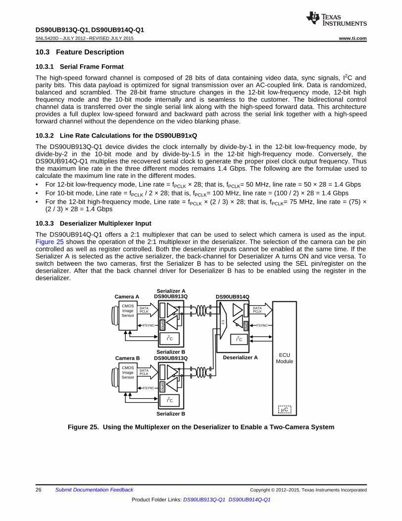
10.1 OverviewThe DS90UB91xQ-Q1 FPD-Link III chipsets are intended to link megapixel camera imagers and videoprocessors in ECUs. The serializer and deserializer chipset can operate from 10-MHz to 100-MHz pixel clockfrequency. The DS90UB913Q-Q1 device transforms a 10- and 12-bit wide parallel LVCMOS data bus along witha bidirectional control channel control bus into a single high-speed differential pair. The high-speed serial bitstream contains an embedded clock and DC-balanced information which enhances signal quality to support ACcoupling. The DS90UB914Q-Q1 device receives the single serial data stream and converts it back into a 10- and12-bit wide parallel data bus together with the control channel data bus. The DS90UB91xQ-Q1 chipsets canaccept up to:• 12 bits of DATA+2 bits SYNC for an input PCLK range of 10 MHz-50 MHz in the 12-bit low-frequency mode• 12 bits DATA + 2 SYNC bits for an input PCLK range of 15 MHz to 75 MHz in the 12-bit high-frequency mode• 10 bits DATA + 2 SYNC bits for an input PCLK range of 20 MHz to 100 MHz in the 10-bit mode.
The DS90UB914Q-Q1 chipset has a 2:1 multiplexer that allows customers to select between two serializerinputs. The control channel function of the DS90UB91xQ-Q1 chipset provides bidirectional communicationbetween the image sensor and ECUs. The integrated bidirectional control channel transfers data bidirectionallyover the same differential pair used for video data interface. This interface offers advantages over other chipsetsby eliminating the need for additional wires for programming and control. The bidirectional control channel bus iscontrolled through an I2C port. The bidirectional control channel offers asymmetrical communication and is notdependent on video blanking intervals.
The DS90UB91xQ-Q1 chipset offer customers the choice to work with different clocking schemes. TheDS90UB91xQ-Q1 chipsets can use an external oscillator as the reference clock source for the PLL or PCLK fromthe imager as primary reference clock to the PLL.
10.2 Functional Block Diagram
Copyright © 2012–2015, Texas Instruments Incorporated Submit Documentation Feedback 25
Product Folder Links: DS90UB913Q-Q1 DS90UB914Q-Q1
DATAPCLK
ECUModule
DS90UB914QDS90UB913Q
CMOSImageSensor
I2C I
2C
PC
DS90UB913Q
CMOSImageSensor
I2C
Camera B
Camera A
FSYNC
FSYNC
GP
IO
GP
IO FSYNC
GP
IO
DATAPCLK
Deserializer ASerializer B
Serializer B
2:1
Serializer A
DATAPCLK
DS90UB913Q-Q1, DS90UB914Q-Q1SNLS420D –JULY 2012–REVISED JULY 2015 www.ti.com
10.3 Feature Description
10.3.1 Serial Frame FormatThe high-speed forward channel is composed of 28 bits of data containing video data, sync signals, I2C andparity bits. This data payload is optimized for signal transmission over an AC-coupled link. Data is randomized,balanced and scrambled. The 28-bit frame structure changes in the 12-bit low-frequency mode, 12-bit highfrequency mode and the 10-bit mode internally and is seamless to the customer. The bidirectional controlchannel data is transferred over the single serial link along with the high-speed forward data. This architectureprovides a full duplex low-speed forward and backward path across the serial link together with a high-speedforward channel without the dependence on the video blanking phase.
10.3.2 Line Rate Calculations for the DS90UB91xQThe DS90UB913Q-Q1 device divides the clock internally by divide-by-1 in the 12-bit low-frequency mode, bydivide-by-2 in the 10-bit mode and by divide-by-1.5 in the 12-bit high-frequency mode. Conversely, theDS90UB914Q-Q1 multiplies the recovered serial clock to generate the proper pixel clock output frequency. Thusthe maximum line rate in the three different modes remains 1.4 Gbps. The following are the formulae used tocalculate the maximum line rate in the different modes.• For 12-bit low-frequency mode, Line rate = fPCLK × 28; that is, fPCLK= 50 MHz, line rate = 50 × 28 = 1.4 Gbps• For 10-bit mode, Line rate = fPCLK / 2 × 28; that is, fPCLK= 100 MHz, line rate = (100 / 2) × 28 = 1.4 Gbps• For the 12-bit high-frequency mode, Line rate = fPCLK × (2 / 3) × 28; that is, fPCLK= 75 MHz, line rate = (75) ×
(2 / 3) × 28 = 1.4 Gbps
10.3.3 Deserializer Multiplexer InputThe DS90UB914Q-Q1 offers a 2:1 multiplexer that can be used to select which camera is used as the input.Figure 25 shows the operation of the 2:1 multiplexer in the deserializer. The selection of the camera can be pincontrolled as well as register controlled. Both the deserializer inputs cannot be enabled at the same time. If theSerializer A is selected as the active serializer, the back-channel for Deserializer A turns ON and vice versa. Toswitch between the two cameras, first the Serializer B has to be selected using the SEL pin/register on thedeserializer. After that the back channel driver for Deserializer B has to be enabled using the register in thedeserializer.
Figure 25. Using the Multiplexer on the Deserializer to Enable a Two-Camera System
26 Submit Documentation Feedback Copyright © 2012–2015, Texas Instruments Incorporated
Product Folder Links: DS90UB913Q-Q1 DS90UB914Q-Q1

Bus Activity:Master
SDA Line
Bus Activity: Slave
Sta
rt
Slave Address
ACK
S
Address
ACK
S
Sta
rt
Slave Address
ACK
NACK
P
Sto
p
Data
0 1
Register
7-bit Address 7-bit Address
ACK
ACK
ACK
S P
Sto
p
Bus Activity: Slave
SDA Line
Bus Activity:Master
Slave Address Address Data
Sta
rt
0
Register
7-bit Address
DS90UB913Q-Q1, DS90UB914Q-Q1www.ti.com SNLS420D –JULY 2012–REVISED JULY 2015
Feature Description (continued)10.3.4 Error DetectionThe chipset provides error detection operations for validating data integrity in long distance transmission andreception. The data error detection function offers users flexibility and usability of performing bit-by-bit datatransmission error checking. The error detection operating modes support data validation of the following signals:• Bidirectional control channel data across the serial link• Parallel video/sync data across the serial link
The chipset provides one parity bit on the forward channel and 4 CRC bits on the back channel for errordetection purposes. The DS90UB91xQ-Q1 chipset checks the forward and back channel serial links for errorsand stores the number of detected errors in two 8-bit registers in the serializer and the deserializer respectively.
To check parity errors on the forward-channel, monitor registers 0x1A and 0x1B on the deserializer. If there is aloss of LOCK, then the counters on registers 0x1A and 0x1B are reset.
NOTEWhenever there is a parity error on the forward channel, the PASS pin will go low.
To check CRC errors on the back-channel, monitor registers 0x0A and 0x0B on the serializer.
10.3.5 Description of Bidirectional Control Bus and I2C ModesThe I2C-compatible interface allows programming of the DS90UB913Q-Q1, DS90UB914Q-Q1, or an externalremote device (such as image sensor) through the bidirectional control channel. Register programmingtransactions to/from the DS90UB913xQ-Q1 chipset are employed through the clock (SCL) and data (SDA) lines.These two signals have open-drain I/Os and both lines must be pulled up to VDDIO by an external resistor.Pullup resistors or current sources are required on the SCL and SDA busses to pull them high when they are notbeing driven low. A logic LOW is transmitted by driving the output low. Logic HIGH is transmitted by releasing theoutput and allowing it to be pulled up externally. The appropriate pullup resistor values will depend upon the totalbus capacitance and operating speed. The DS90UB91xQ-Q1 I2C bus data rate supports up to 400 kbpsaccording to I2C fast mode specifications.
Figure 26. Write Byte
Figure 27. Read Byte
Copyright © 2012–2015, Texas Instruments Incorporated Submit Documentation Feedback 27
Product Folder Links: DS90UB913Q-Q1 DS90UB914Q-Q1
SDA
SCL
S P
START condition, orSTART repeat condition
STOP condition
SCL
SDA
START STOP
1 2 6 7 8 9 1 2 8 9
MSB
7-bit Slave Address
R/W Direction
BitAcknowledge
from the Device
MSB
Data Byte
*Acknowledgeor Not-ACK
ACK N/ACK
Repeated for the Lower Data Byte and Additional Data Transfers
LSB LSB
DS90UB913Q-Q1, DS90UB914Q-Q1SNLS420D –JULY 2012–REVISED JULY 2015 www.ti.com
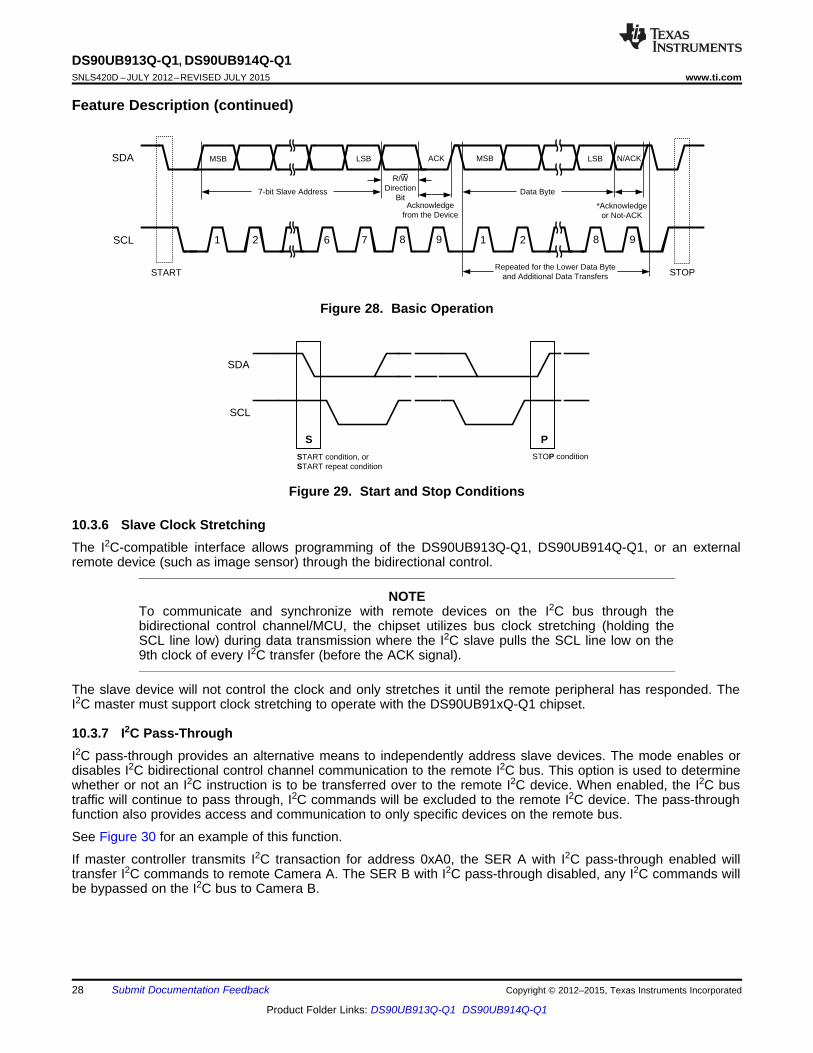
Feature Description (continued)
Figure 28. Basic Operation
Figure 29. Start and Stop Conditions
10.3.6 Slave Clock StretchingThe I2C-compatible interface allows programming of the DS90UB913Q-Q1, DS90UB914Q-Q1, or an externalremote device (such as image sensor) through the bidirectional control.
NOTETo communicate and synchronize with remote devices on the I2C bus through thebidirectional control channel/MCU, the chipset utilizes bus clock stretching (holding theSCL line low) during data transmission where the I2C slave pulls the SCL line low on the9th clock of every I2C transfer (before the ACK signal).
The slave device will not control the clock and only stretches it until the remote peripheral has responded. TheI2C master must support clock stretching to operate with the DS90UB91xQ-Q1 chipset.
10.3.7 I2C Pass-ThroughI2C pass-through provides an alternative means to independently address slave devices. The mode enables ordisables I2C bidirectional control channel communication to the remote I2C bus. This option is used to determinewhether or not an I2C instruction is to be transferred over to the remote I2C device. When enabled, the I2C bustraffic will continue to pass through, I2C commands will be excluded to the remote I2C device. The pass-throughfunction also provides access and communication to only specific devices on the remote bus.
See Figure 30 for an example of this function.
If master controller transmits I2C transaction for address 0xA0, the SER A with I2C pass-through enabled willtransfer I2C commands to remote Camera A. The SER B with I2C pass-through disabled, any I2C commands willbe bypassed on the I2C bus to Camera B.
28 Submit Documentation Feedback Copyright © 2012–2015, Texas Instruments Incorporated
Product Folder Links: DS90UB913Q-Q1 DS90UB914Q-Q1

HOST DS90UB913Q
SCL
SDA
RPU RPU
10k
RID
SCL
SDA
To other Devices
ID[x]
1.8V
VDDIO
ECUModule
DS90UB914QDS90UB913Q
DIN[11:0],HS,VSPCLK
CMOSImageSensor
I2C
ROUT[11:0],HS,VS,PCLK
I2CSDA
SCLSDASCL
PC
DES B: I2C_SLAVE
DS90UB914QDS90UB913Q
DIN[11:0],HS,VSPCLK
CMOSImageSensor
I2C
ROUT[11:0],HS,VS,PCLK
I2CSDA
SCLSDASCL
Camera BSlave ID: (0xA0)
SER A: I2C _MASTERI2C_PASS_THRU Enabled
DES A: I2C_SLAVECamera A
Slave ID: (0xA0)
MasterSER B: I2C_MASTERI2C_PASS_THRU Disabled
DS90UB913Q-Q1, DS90UB914Q-Q1www.ti.com SNLS420D –JULY 2012–REVISED JULY 2015
Feature Description (continued)
Figure 30. I2C Pass-Through
10.3.8 ID[x] Address Decoder on the SerializerThe ID[x] pin on the serializer is used to decode and set the physical slave address of the serializer (I2C only) toallow up to five devices on the bus connected to the serializer using only a single pin. The pin sets one of the 5possible addresses for each serializer device. The pin must be pulled to VDD (1.8 V, not VDDIO) with a 10-kΩresistor and a pulldown resistor (RID) of the recommended value to set the physical device address. Therecommended maximum resistor tolerance is 1%.
Figure 31. ID[x] Address Decoder on the Serializer
Copyright © 2012–2015, Texas Instruments Incorporated Submit Documentation Feedback 29
Product Folder Links: DS90UB913Q-Q1 DS90UB914Q-Q1

HOST DS90UB914Q
SCL
SDA
RPU RPU
10k
RID0
SCL
SDA
To otherDevices
IDx[0]
1.8V
VDDIO
10k
RID1
1.8V
IDx[1]
DS90UB913Q-Q1, DS90UB914Q-Q1SNLS420D –JULY 2012–REVISED JULY 2015 www.ti.com
Table 1. ID[x] Resistor Value for DS90UB913Q-Q1 SerializerID[x] Resistor Value — DS90UB913Q-Q1 Serializer
Resistor RID0 Ω Address 8'b 0 appendedAddress 7'b(1% Tolerance) (WRITE)0 k 0x58 0xB02 k 0x59 0xB2
4.7 k 0x5A 0xB48.2 k 0x5B 0xB614 k 0x5C 0xB8100 k 0x5D 0xBA
10.3.9 ID[x] Address Decoder on the DeserializerThe IDx[0] and IDx[1] pins on the deserializer are used to decode and set the physical slave address of thedeserializer (I2C only) to allow up to 16 devices on the bus using only two pins. The pins set one of 16 possibleaddresses for each deserializer device. As there will be more deserializer devices connected on the same boardthan serializers, more I2C device addresses have been defined for the DS90UB914Q-Q1 deserializer than theDSDS90UB913Q-Q1 serializer. The pins must be pulled to VDD (1.8 V, not VDDIO) with a 10-kΩ resistor andtwo pulldown resistors (RID0 and RID1) of the recommended value to set the physical device address. Therecommended maximum resistor tolerance is 1%.
Figure 32. ID[x[ Address Decoder on the Deserializer
Table 2. Resistor Values for IDx[0] and IDx[1] on DS90UB914Q-Q1 DeserializerID[X] RESISTOR VALUE — DS90UB913Q SERIALIZER
RESISTOR RID1 Ω RESISTOR RID0 Ω ADDRESS 8'b 0 APPENDEDADDRESS 7'b(1%TOLERANCE) (1%TOLERANCE) (WRITE)0 k 0 k 0x60 0xC00 k 3 k 0x61 0xC20 k 11 k 0x62 0xC40 k 100 k 0x63 0xC63 k 0 k 0x64 0xC8
30 Submit Documentation Feedback Copyright © 2012–2015, Texas Instruments Incorporated
Product Folder Links: DS90UB913Q-Q1 DS90UB914Q-Q1

DS90UB913Q-Q1, DS90UB914Q-Q1www.ti.com SNLS420D –JULY 2012–REVISED JULY 2015
Table 2. Resistor Values for IDx[0] and IDx[1] on DS90UB914Q-Q1 Deserializer (continued)ID[X] RESISTOR VALUE — DS90UB913Q SERIALIZER
3 k 3 k 0x65 0xCA3 k 11 k 0x66 0XCC3 k 100 k 0x67 0XCE11 k 0 k 0x68 0XD011 k 3 k 0x69 0XD211 k 11 k 0x6A 0XD411 k 100 k 0x6B 0XD6100 k 0 k 0x6C 0XD8100 k 3 k 0x6D 0XDA100 k 11 k 0x6E 0XDC100 k 100 k 0x6F 0XDE
10.3.10 Programmable ControllerAn integrated I2C slave controller is embedded in the DS90UB913Q-Q1 serializer as well as the DS90UB914Q-Q1 deserializer. It must be used to configure the extra features embedded within the programmable registers or itcan be used to control the set of programmable GPIOs.
10.3.11 Synchronizing Multiple CamerasFor applications requiring multiple cameras for frame-synchronization, TI recommends to utilize the General-Purpose Input/Output (GPIO) pins to transmit control signals to synchronize multiple cameras together. Tosynchronize the cameras properly, the system controller needs to provide a field sync output (such as a verticalor frame sync signal) and the cameras must be set to accept an auxiliary sync input. The vertical synchronizesignal corresponds to the start and end of a frame and the start and end of a field.
NOTEthis form of synchronization timing relationship has a non-deterministic latency. After thecontrol data is reconstructed from the bidirectional control channel, there will be a timevariation of the GPIO signals arriving at the different target devices (between the parallellinks). The maximum latency delta (t1) of the GPIO data transmitted across multiple linksis 25 µs.
NOTEThe user must verify that the timing variations between the different links are within theirsystem and timing specifications.
Copyright © 2012–2015, Texas Instruments Incorporated Submit Documentation Feedback 31
Product Folder Links: DS90UB913Q-Q1 DS90UB914Q-Q1

DES AGPIO[n] Input
DES BGPIO[n] Input
SER AGPIO[n] Output
SER BGPIO[n] Output
t1
||
ECUModule
DS90UB914QDS90UB913Q
CMOSImageSensor
I2C I
2C
PC
DS90UB914QDS90UB913Q
CMOSImageSensor
I2C I
2C
Camera B
Camera A
DATAPCLK
DATAPCLK
FSYNC
FSYNC
GP
O
GP
IO FSYNC
GP
O
GP
IO FSYNC
DATAPCLK
DATAPCLK
FS
OF
SO
FS
INF
SIN
Deserializer ASerializer A
Deserializer BSerializer B
DS90UB913Q-Q1, DS90UB914Q-Q1SNLS420D –JULY 2012–REVISED JULY 2015 www.ti.com
See Figure 33 for an example of synchronizing multiple cameras.
The maximum time (t1) between the rising edge of GPIO (that is, sync signal) arriving at Camera A and CameraB is 25 µs.
Figure 33. Synchronizing Multiple Cameras
Figure 34. GPIO Delta Latency
10.3.12 General-Purpose I/O (GPIO) DescriptionsThere are 4 GPOs on the serializer and 4 GPIOs on the deserializer when the DS90UB91xQ-Q1 chipsets are runoff the pixel clock from the imager as the reference clock source. The GPOs on the serializer can be configuredas outputs for the input signals that are fed into the deserializer GPIOs. In addition, the GPOs on the serializercan behave as outputs of the local register on the serializer. The GPIOs on the deserializer can be configured tobe the input signals feeding the output of the GPOs on the serializer. In addition the GPIOs on the deserializercan be configured to behave as outputs of the local register on the deserializer. If the DS90UB91xQ-Q1 chipsetsare run off the external oscillator source as the reference clock, then GPO3 on the serializer is automaticallyconfigured to be the input for the external clock and GPIO2 on the deserializer is configured to be the output ofthe divide-by-2 clock which is fed into the imager as its reference clock. In this case, the GPIO2 and GPIO3 onthe deserializer can only behave as outputs of the local register on the deserializer. The GPIO maximumswitching rate is up to 66 kHz when configured for communication between deserializer GPIO to serializer GPO.
32 Submit Documentation Feedback Copyright © 2012–2015, Texas Instruments Incorporated
Product Folder Links: DS90UB913Q-Q1 DS90UB914Q-Q1

600
SERIAL LINE FREQUENCY (MHz)
0
2
4
6
8
10
12
14
16
18
EQ
UA
LIZ
ER
GA
IN (
dB)
700500400300200100
DS90UB913Q-Q1, DS90UB914Q-Q1www.ti.com SNLS420D –JULY 2012–REVISED JULY 2015
10.3.13 LVCMOS VDDIO Option1.8-V, 2.8-V, and 3.3-V serializer inputs and 1.8-V and 3.3-V deserializer outputs are user configurable to providecompatibility with 1.8-V, 2.8-V and 3.3-V system interfaces.
10.3.14 Deserializer – Adaptive Input Equalization (AEQ)The receiver inputs provide an adaptive input equalization filter in order to compensate for loss from the media.The level of equalization can also be manually selected through register controls. The fully-adaptive equalizeroutput can be seen using the CMLOUTP/CMLOUTN pins in the deserializer.
Figure 35. Maximum Equalizer Gain vs. Line Frequency
10.3.15 EMI Reduction
10.3.15.1 Deserializer Staggered OutputThe receiver staggers output switching to provide a random distribution of transitions within a defined window.Outputs transitions are distributed randomly. This minimizes the number of outputs switching simultaneously andhelps to reduce supply noise. In addition it spreads the noise spectrum out reducing overall EMI.
10.3.15.2 Spread Spectrum Clock Generation (SSCG) on the DeserializerThe DS90UB914Q-Q1 parallel data and clock outputs have programmable SSCG ranges from 10 MHz to 100MHz. The modulation rate and modulation frequency variation of output spread is controlled through the SSCcontrol registers on the DS90UB914Q-Q1 device. SSC profiles can be generated using bits [3:0] in register 0x02in the deserializer.
10.4 Device Functional Modes
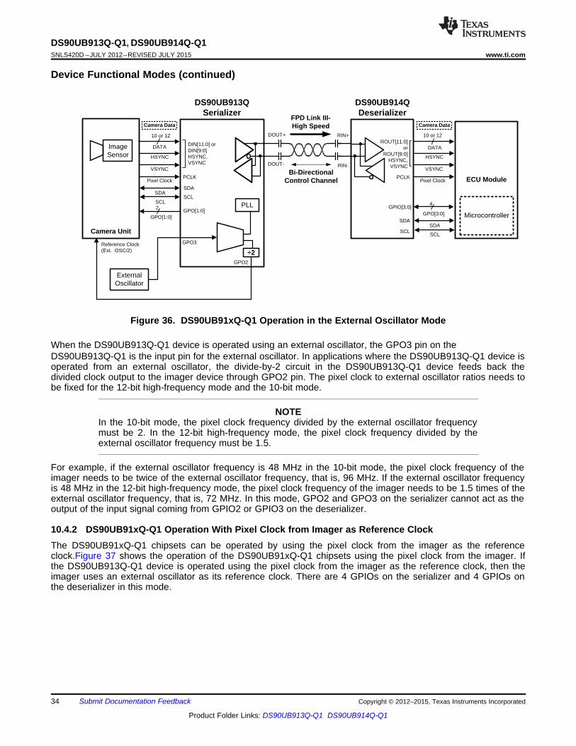
10.4.1 DS90UB91xQ-Q1 Operation With External Oscillator as Reference ClockIn some applications, the pixel clock that comes from the imager can have jitter which exceeds the tolerance ofthe DS90UB91xQ-Q1 chipsets. In this case, the DS90UB913Q-Q1 device should be operated by using anexternal clock source as the reference clock for the DS90UB91xQ-Q1 chipsets. This is the recommendedoperating mode. The external oscillator clock output goes through a divide-by-2 circuit in the DS90UB913Q-Q1serializer and this divided clock output is used as the reference clock for the imager. The output data and pixelclock from the imager are then fed into the DS90UB913Q-Q1 device. Figure 36 shows the operation of theDS90UB1xQ-Q1 chipsets while using an external automotive grade oscillator.
Copyright © 2012–2015, Texas Instruments Incorporated Submit Documentation Feedback 33
Product Folder Links: DS90UB913Q-Q1 DS90UB914Q-Q1
FPD Link III-High Speed
Bi-DirectionalControl Channel
Image Sensor
ECU Module
DIN[11:0] or DIN[9:0]HSYNC, VSYNC
SDA
SCL
DOUT- RIN-
DOUT+ RIN+
Camera Unit
10 or 12
DATA
HSYNC
VSYNC
PCLKPixel Clock
SDA
SCL
Microcontroller
ROUT[11:0] or
ROUT[9:0] HSYNC, VSYNC
SDA
SCL
PCLK
10 or 12
DATA
HSYNC
VSYNC
Pixel Clock
SDA
SCL
Camera Data
DS90UB914QDeserializer
DS90UB913QSerializer
GPO[1:0]GPO[1:0]2
GPO[3:0]
4GPIO[3:0]
Camera Data
External Oscillator
PLL
÷2
GPO3
GPO2
Reference Clock (Ext. OSC/2)
DS90UB913Q-Q1, DS90UB914Q-Q1SNLS420D –JULY 2012–REVISED JULY 2015 www.ti.com
Device Functional Modes (continued)
Figure 36. DS90UB91xQ-Q1 Operation in the External Oscillator Mode
When the DS90UB913Q-Q1 device is operated using an external oscillator, the GPO3 pin on theDS90UB913Q-Q1 is the input pin for the external oscillator. In applications where the DS90UB913Q-Q1 device isoperated from an external oscillator, the divide-by-2 circuit in the DS90UB913Q-Q1 device feeds back thedivided clock output to the imager device through GPO2 pin. The pixel clock to external oscillator ratios needs tobe fixed for the 12-bit high-frequency mode and the 10-bit mode.
NOTEIn the 10-bit mode, the pixel clock frequency divided by the external oscillator frequencymust be 2. In the 12-bit high-frequency mode, the pixel clock frequency divided by theexternal oscillator frequency must be 1.5.
For example, if the external oscillator frequency is 48 MHz in the 10-bit mode, the pixel clock frequency of theimager needs to be twice of the external oscillator frequency, that is, 96 MHz. If the external oscillator frequencyis 48 MHz in the 12-bit high-frequency mode, the pixel clock frequency of the imager needs to be 1.5 times of theexternal oscillator frequency, that is, 72 MHz. In this mode, GPO2 and GPO3 on the serializer cannot act as theoutput of the input signal coming from GPIO2 or GPIO3 on the deserializer.
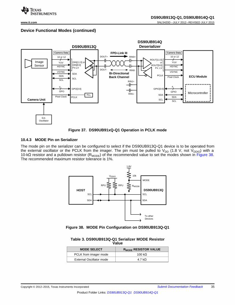
10.4.2 DS90UB91xQ-Q1 Operation With Pixel Clock from Imager as Reference ClockThe DS90UB91xQ-Q1 chipsets can be operated by using the pixel clock from the imager as the referenceclock.Figure 37 shows the operation of the DS90UB91xQ-Q1 chipsets using the pixel clock from the imager. Ifthe DS90UB913Q-Q1 device is operated using the pixel clock from the imager as the reference clock, then theimager uses an external oscillator as its reference clock. There are 4 GPIOs on the serializer and 4 GPIOs onthe deserializer in this mode.
34 Submit Documentation Feedback Copyright © 2012–2015, Texas Instruments Incorporated
Product Folder Links: DS90UB913Q-Q1 DS90UB914Q-Q1
DS90UB913QHOSTSCL
SDA
RPU RPU
10k
RMODE
SCL
SDA
To other Devices
MODE
1.8V
VDDIO
FPD-Link III
Bi-DirectionalBack Channel
Image Sensor
ECU Module
DIN[11:0] or DIN[9:0]FV,LV
SDA
SCL
DOUT- RIN0-
DOUT+ RIN0+
Camera Unit
10 or 12
YUV
HSYNC
VSYNC
PCLKPixel Clock
SDA
SCL
Microcontroller
ROUT[11:0] or
ROUT[9:0] FV, LV
SDA
SCL
PCLK
10 or 12
YUV
HSYNC
VSYNC
Pixel Clock
SDA
SCL
Camera Data
DS90UB914QDeserializerDS90UB913Q
GPOGPO[3:0]
4
GPIO
4GPIO[3:0]
Camera Data
Ext. Oscillator
PLL RIN1-
RIN1+
DS90UB913Q-Q1, DS90UB914Q-Q1www.ti.com SNLS420D –JULY 2012–REVISED JULY 2015
Device Functional Modes (continued)
Figure 37. DS90UB91xQ-Q1 Operation in PCLK mode
10.4.3 MODE Pin on SerializerThe mode pin on the serializer can be configured to select if the DS90UB913Q-Q1 device is to be operated fromthe external oscillator or the PCLK from the imager. The pin must be pulled to VDD (1.8 V, not VDDIO) with a10-kΩ resistor and a pulldown resistor (RMODE) of the recommended value to set the modes shown in Figure 38.The recommended maximum resistor tolerance is 1%.
Figure 38. MODE Pin Configuration on DS90UB913Q-Q1
Table 3. DS90UB913Q-Q1 Serializer MODE ResistorValue
MODE SELECT RMODE RESISTOR VALUEPCLK from imager mode 100 kΩExternal Oscillator mode 4.7 kΩ
Copyright © 2012–2015, Texas Instruments Incorporated Submit Documentation Feedback 35
Product Folder Links: DS90UB913Q-Q1 DS90UB914Q-Q1

HOST DS90UB914QSCL
SDA
RPU RPU
10k
RMODE
SCL
SDA
To Other Devices
MODE
1.8V
VDDIO
DS90UB913Q-Q1, DS90UB914Q-Q1SNLS420D –JULY 2012–REVISED JULY 2015 www.ti.com
10.4.4 MODE Pin on DeserializerThe mode pin on the deserializer can be used to configure the device to work in the 12-bit low-frequency mode,12-bit high frequency mode or the 10-bit mode of operation. Internally, the DS90UB91xQ-Q1 chipset operates ina divide-by-1 mode in the 12-bit low-frequency mode, divide-by-2 mode in the 10-bit mode and a divide-by-1.5mode in the 12-bit high-frequency mode. The pin must be pulled to VDD (1.8 V, not VDDIO) with a 10-kΩ resistorand a pulldown resistor (RMODE) of the recommended value to set the different modes in the deserializer asmentioned in Table 4. The deserializer automatically configures the serializer to correct mode through the back-channel. The recommended maximum resistor tolerance is 1%
.
Figure 39. Mode Pin Configuration on DS90UB914Q-Q1 Deserializer
Table 4. DS90UB914Q-Q1 Deserializer MODE ResistorValue
DS90UB914Q-Q1 DESERIALIZER MODE RESISTOR VALUEMODE SELECT RMODE RESISTOR VALUE
12-bit low-frequency mode10 to 50 MHz PCLK 0 Ω
10 to 12 bit DATA + 2 SYNC12-bit low-frequency mode
15 to 75 MHz PCLK 3 kΩ10 to 12 bit DATA + 2 SYNC
10-bit mode20 to 100 MHz PCLK 11 kΩ
10 to 10 bit DATA + 2 SYNC
36 Submit Documentation Feedback Copyright © 2012–2015, Texas Instruments Incorporated
Product Folder Links: DS90UB913Q-Q1 DS90UB914Q-Q1
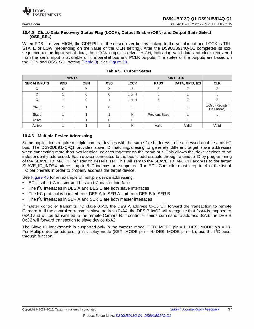
DS90UB913Q-Q1, DS90UB914Q-Q1www.ti.com SNLS420D –JULY 2012–REVISED JULY 2015
10.4.5 Clock-Data Recovery Status Flag (LOCK), Output Enable (OEN) and Output State Select(OSS_SEL)
When PDB is driven HIGH, the CDR PLL of the deserializer begins locking to the serial input and LOCK is TRI-STATE or LOW (depending on the value of the OEN setting). After the DS90UB914Q-Q1 completes its locksequence to the input serial data, the LOCK output is driven HIGH, indicating valid data and clock recoveredfrom the serial input is available on the parallel bus and PCLK outputs. The states of the outputs are based onthe OEN and OSS_SEL setting (Table 3). See Figure 20.
Table 5. Output StatesINPUTS OUTPUTS
SERIAI INPUTS PDB OEN OSS LOCK PASS DATA, GPIO, I2S CLKX 0 X X Z Z Z ZX 1 0 0 L or H L L LX 1 0 1 L or H Z Z Z
L/Osc (RegisterStatic 1 1 0 L L L Bit Enable)Static 1 1 1 H Previous State L LActive 1 1 0 H L L LActive 1 1 1 H Valid Valid Valid
10.4.6 Multiple Device AddressingSome applications require multiple camera devices with the same fixed address to be accessed on the same I2Cbus. The DS90UB91xQ-Q1 provides slave ID matching/aliasing to generate different target slave addresseswhen connecting more than two identical devices together on the same bus. This allows the slave devices to beindependently addressed. Each device connected to the bus is addressable through a unique ID by programmingof the SLAVE_ID_MATCH register on deserializer. This will remap the SLAVE_ID_MATCH address to the targetSLAVE_ID_INDEX address; up to 8 ID indexes are supported. The ECU Controller must keep track of the list ofI2C peripherals in order to properly address the target device.
See Figure 40 for an example of multiple device addressing.• ECU is the I2C master and has an I2C master interface• The I2C interfaces in DES A and DES B are both slave interfaces• The I2C protocol is bridged from DES A to SER A and from DES B to SER B• The I2C interfaces in SER A and SER B are both master interfaces
If master controller transmits I2C slave 0xA0, the DES A address 0xC0 will forward the transaction to remoteCamera A. If the controller transmits slave address 0xA4, the DES B 0xC2 will recognize that 0xA4 is mapped to0xA0 and will be transmitted to the remote Camera B. If controller sends command to address 0xA6, the DES B0xC2 will forward transaction to slave device 0xA2.
The Slave ID index/match is supported only in the camera mode (SER: MODE pin = L; DES: MODE pin = H).For Multiple device addressing in display mode (SER: MODE pin = H; DES: MODE pin = L), use the I2C pass-through function.
Copyright © 2012–2015, Texas Instruments Incorporated Submit Documentation Feedback 37
Product Folder Links: DS90UB913Q-Q1 DS90UB914Q-Q1

DIN/ROUT
PCLK
TRFB/RRFB: 0 TRFB/RRFB: 1
ECUModule
DS90UB914QDS90UB913Q
DIN[11:0], HS, VS,
PCLK
CMOSImageSensor
I2C I
2CSDA
SCLSDASCL
PC
DES B: ID[x](0xC2)SLAVE_ID2_MATCH(0xA4)SLAVE_ID2_INDEX(0xA0)
SLAVE_ID2_MATCH(0xA6)SLAVE_ID2_INDEX(0xA2)
DS90UB914QDS90UB913Q
CMOSImageSensor
I2C I
2CSDA
SCLSDASCL
Camera BSlave ID: (0xA0)
SER A: ID[x](0xB0) DES A: ID[x](0xC0)SLAVE_ID1_MATCH(0xA0)SLAVE_ID1_INDEX(0xA0)
SLAVE_ID2_MATCH(0xA2)SLAVE_ID2_INDEX(0xA2)
Camera ASlave ID: (0xA0)
MasterSER B: ID[x](0xB2)
Slave ID: (0xA2)
Slave ID: (0xA2)
PC/ EEPROM
PC/ EEPROM
ROUT[11:0], HS, VS,PCLK
DIN[11:0], HS, VS,
PCLK
ROUT[11:0], HS, VS,PCLK
DS90UB913Q-Q1, DS90UB914Q-Q1SNLS420D –JULY 2012–REVISED JULY 2015 www.ti.com
Figure 40. Multiple Device Addressing
10.4.7 PowerdownThe SER has a PDB input pin to ENABLE or Powerdown (SLEEP) the device. The modes can be controlled bythe host and is used to disable the Link to save power when the remote device is not operational. In this mode, ifthe PDB pin is tied High and the SER will enter SLEEP when the PCLK stops. When the PCLK starts again, theSER will then lock to the valid input PCLK and transmit the data to the DES. In SLEEP mode, the high-speeddriver outputs are static (High). The DES has a PDB input pin to ENABLE or Powerdown (SLEEP) the device.This pin can be controlled by the system and is used to disable the DES to save power. An auto mode is alsoavailable. In this mode, the PDB pin is tied High and the DES will enter SLEEP when the serial stream stops.When the serial stream starts up again, the DES will lock to the input stream and assert the LOCK pin and outputvalid data. In SLEEP mode, the Data and PCLK outputs are set by the OSS_SEL configuration.
10.4.8 Pixel Clock Edge Select (TRFB / RRFB)The TRFB/RRFB selects which edge of the Pixel Clock is used. For the SER, this register determines the edgethat the data is latched on. If TRFB register is 1, data is latched on the Rising edge of the PCLK. If TRFB registeris 0, data is latched on the Falling edge of the PCLK. For the DES, this register determines the edge that thedata is strobed on. If RRFB register is 1, data is strobed on the Rising edge of the PCLK. If RRFB register is 0,data is strobed on the falling edge of the PCLK.
Figure 41. Programmable PCLK Strobe Select
38 Submit Documentation Feedback Copyright © 2012–2015, Texas Instruments Incorporated
Product Folder Links: DS90UB913Q-Q1 DS90UB914Q-Q1
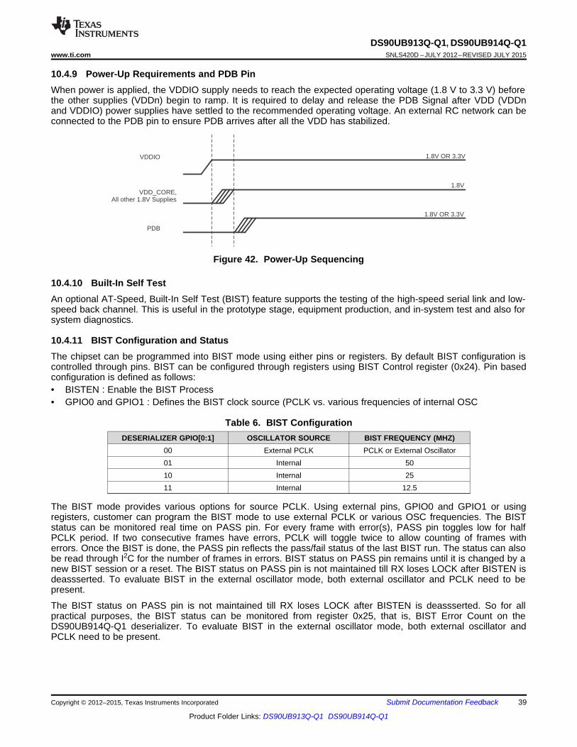
VDDIO
All other 1.8V SuppliesVDD_CORE,
PDB
1.8V OR 3.3V
1.8V
1.8V OR 3.3V
DS90UB913Q-Q1, DS90UB914Q-Q1www.ti.com SNLS420D –JULY 2012–REVISED JULY 2015
10.4.9 Power-Up Requirements and PDB PinWhen power is applied, the VDDIO supply needs to reach the expected operating voltage (1.8 V to 3.3 V) beforethe other supplies (VDDn) begin to ramp. It is required to delay and release the PDB Signal after VDD (VDDnand VDDIO) power supplies have settled to the recommended operating voltage. An external RC network can beconnected to the PDB pin to ensure PDB arrives after all the VDD has stabilized.
Figure 42. Power-Up Sequencing
10.4.10 Built-In Self TestAn optional AT-Speed, Built-In Self Test (BIST) feature supports the testing of the high-speed serial link and low-speed back channel. This is useful in the prototype stage, equipment production, and in-system test and also forsystem diagnostics.
10.4.11 BIST Configuration and StatusThe chipset can be programmed into BIST mode using either pins or registers. By default BIST configuration iscontrolled through pins. BIST can be configured through registers using BIST Control register (0x24). Pin basedconfiguration is defined as follows:• BISTEN : Enable the BIST Process• GPIO0 and GPIO1 : Defines the BIST clock source (PCLK vs. various frequencies of internal OSC
Table 6. BIST ConfigurationDESERIALIZER GPIO[0:1] OSCILLATOR SOURCE BIST FREQUENCY (MHZ)
00 External PCLK PCLK or External Oscillator01 Internal 5010 Internal 2511 Internal 12.5
The BIST mode provides various options for source PCLK. Using external pins, GPIO0 and GPIO1 or usingregisters, customer can program the BIST mode to use external PCLK or various OSC frequencies. The BISTstatus can be monitored real time on PASS pin. For every frame with error(s), PASS pin toggles low for halfPCLK period. If two consecutive frames have errors, PCLK will toggle twice to allow counting of frames witherrors. Once the BIST is done, the PASS pin reflects the pass/fail status of the last BIST run. The status can alsobe read through I2C for the number of frames in errors. BIST status on PASS pin remains until it is changed by anew BIST session or a reset. The BIST status on PASS pin is not maintained till RX loses LOCK after BISTEN isdeassserted. To evaluate BIST in the external oscillator mode, both external oscillator and PCLK need to bepresent.
The BIST status on PASS pin is not maintained till RX loses LOCK after BISTEN is deassserted. So for allpractical purposes, the BIST status can be monitored from register 0x25, that is, BIST Error Count on theDS90UB914Q-Q1 deserializer. To evaluate BIST in the external oscillator mode, both external oscillator andPCLK need to be present.
Copyright © 2012–2015, Texas Instruments Incorporated Submit Documentation Feedback 39
Product Folder Links: DS90UB913Q-Q1 DS90UB914Q-Q1
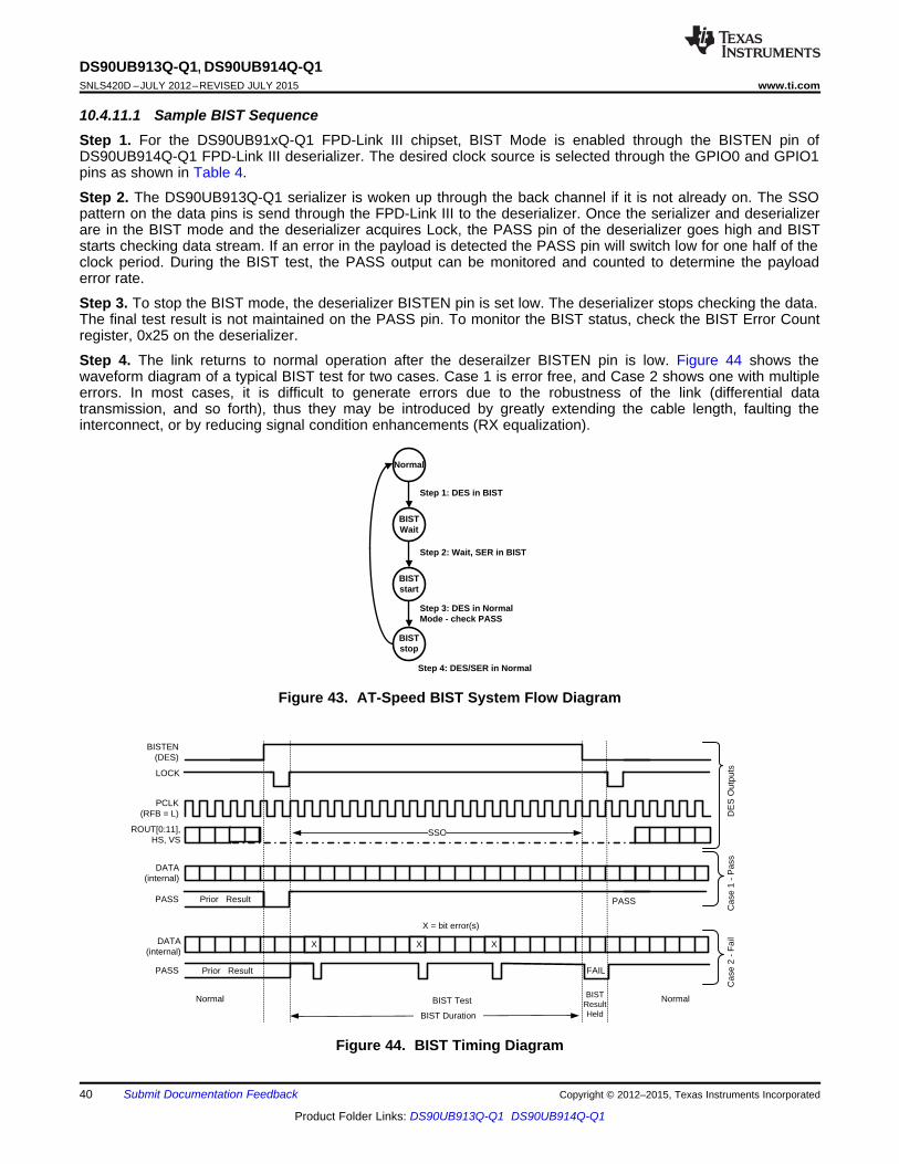
X XX
PCLK(RFB = L)
BISTEN(DES)
PASS
DATA(internal)
PASS
BIST Duration
Prior Result
BIST ResultHeld
PASS
FAIL
X = bit error(s)
ROUT[0:11], HS, VS
DATA(internal)
Cas
e 1
- P
ass
Cas
e 2
- F
ail
Prior Result
Normal BIST Test Normal
DE
S O
utpu
tsLOCK
SSO
Normal
BISTstart
BISTstop
BISTWait
Step 1: DES in BIST
Step 2: Wait, SER in BIST
Step 3: DES in Normal Mode - check PASS
Step 4: DES/SER in Normal
DS90UB913Q-Q1, DS90UB914Q-Q1SNLS420D –JULY 2012–REVISED JULY 2015 www.ti.com
10.4.11.1 Sample BIST SequenceStep 1. For the DS90UB91xQ-Q1 FPD-Link III chipset, BIST Mode is enabled through the BISTEN pin ofDS90UB914Q-Q1 FPD-Link III deserializer. The desired clock source is selected through the GPIO0 and GPIO1pins as shown in Table 4.
Step 2. The DS90UB913Q-Q1 serializer is woken up through the back channel if it is not already on. The SSOpattern on the data pins is send through the FPD-Link III to the deserializer. Once the serializer and deserializerare in the BIST mode and the deserializer acquires Lock, the PASS pin of the deserializer goes high and BISTstarts checking data stream. If an error in the payload is detected the PASS pin will switch low for one half of theclock period. During the BIST test, the PASS output can be monitored and counted to determine the payloaderror rate.
Step 3. To stop the BIST mode, the deserializer BISTEN pin is set low. The deserializer stops checking the data.The final test result is not maintained on the PASS pin. To monitor the BIST status, check the BIST Error Countregister, 0x25 on the deserializer.
Step 4. The link returns to normal operation after the deserailzer BISTEN pin is low. Figure 44 shows thewaveform diagram of a typical BIST test for two cases. Case 1 is error free, and Case 2 shows one with multipleerrors. In most cases, it is difficult to generate errors due to the robustness of the link (differential datatransmission, and so forth), thus they may be introduced by greatly extending the cable length, faulting theinterconnect, or by reducing signal condition enhancements (RX equalization).
Figure 43. AT-Speed BIST System Flow Diagram
Figure 44. BIST Timing Diagram
40 Submit Documentation Feedback Copyright © 2012–2015, Texas Instruments Incorporated
Product Folder Links: DS90UB913Q-Q1 DS90UB914Q-Q1

DS90UB913Q-Q1, DS90UB914Q-Q1www.ti.com SNLS420D –JULY 2012–REVISED JULY 2015
10.5 Register Maps
Table 7. DS90UB913Q-Q1 Control RegistersADDR NAME BITS FIELD R/W DEFAULT DESCRIPTION(HEX)
7-bit address of serializer; 0x58'h7:1 DEVICE ID (0101_1000X'b) default0x00 I2C Device ID RW 0x58'h
0: Device ID is from ID[x]0 SER ID SEL 1: Register I2C Device ID overrides ID[x]7 RSVD Reserved
Digital Output Drive Strength6 RDS RW 0 1: High Drive Strength
0: Low Drive StrengthAuto Voltage Control
5 VDDIO Control RW 1 1: Enable0: DisableVDDIOVoltage set
4 VDDIO MODE RW 1 0: 1.8V1: 3.3VThis register can be set only through local I2C access0x01 Power and Reset1: Analog power-down : Powers Down the analog block3 ANAPWDN RW 0 in the serializer0: No effect
2 RSVD RW 0 Reserved1: Resets the digital block except for register values
DIGITAL values. Does not affect device I2C Bus or Device ID.1 RW 0RESET1 This bit is self-clearing.0: Normal Operation1: Digital Reset, resets the entire digital block including
0 DIGITAL RESET0 RW 1 all register values.This bit is self-clearing.0: Normal Operation.
0x02 RESERVEDBack-channel CRC Checker EnableRX CRC Checker7 RW 1 1:EnabledEnable 0:DisabledForward channel Parity Generator EnableTX Parity Generator6 RW 1 1: EnableEnable 0: DisableClear CRC Error Counters.This bit is NOT self-clearing.5 CRC Error Reset RW 0 1: Clear Counters0: Normal OperationAutomatically Acknowledge I2C Remote WriteThe mode works when the system is LOCKed.1: Enable: When enabled, I2C writes to the deserializer
General I2C Remote Write (or any remote I2C Slave, if I2C PASS ALL is enabled)0x03 4 RW 0Configuration Auto Acknowledge are immediately acknowledged without waiting for thedeserializer to acknowledge the write. The accesses arethen re-mapped to address specified in 0x06.0: Disable1: Enable Forward Control Channel pass-through of allI2C accesses to I2C Slave IDs that do not match theSerializer I2C Slave ID. The I2C accesses are then
3 I2C Pass All RW 0 remapped to address specified in register 0x06.0: Enable Forward Control Channel pass-through only ofI2C accesses to I2C Slave IDs matching either theremote Deserializer Slave ID or the remote Slave ID.I2C Pass-Through Mode
2 I2C PASSTHROUGH RW 1 0: Pass-Through Disabled1: Pass-Through Enabled
Copyright © 2012–2015, Texas Instruments Incorporated Submit Documentation Feedback 41
Product Folder Links: DS90UB913Q-Q1 DS90UB914Q-Q1

DS90UB913Q-Q1, DS90UB914Q-Q1SNLS420D –JULY 2012–REVISED JULY 2015 www.ti.com
Register Maps (continued)Table 7. DS90UB913Q-Q1 Control Registers (continued)
ADDR NAME BITS FIELD R/W DEFAULT DESCRIPTION(HEX)1:Enabled : When enabled this registers overrides theclock to PLL mode (External Oscillator mode or DirectPCLK mode) defined through MODE pin and allows
1 OV_CLK2PLL RW 0 selection through register 0x35 in the serializer0: Disabled : When disabled, Clock to PLL mode(External Oscillator mode or Direct PCLK mode) isGeneral0x03 defined through MODE pin on the serializer.ConfigurationPixel Clock Edge Select1: Parallel Interface Data is strobed on the Rising Clock
0 TRFB RW 1 Edge.0: Parallel Interface Data is strobed on the Falling ClockEdge.
0x04 RESERVED7 RSVD RW 0 Reserved6 RSVD RW 0 Reserved.
Allows overriding mode select bits coming from back-channel5 MODE_OVERRIDE RW 0 1: Overrides MODE select bits0: Does not override MODE select bits
0x05 Mode Select Indicates that the status of mode select from deserializer4 MODE_UP To DATE R 0 is up to datePin_MODE_12–bit 1: 12-bit high-frequency mode is selected.3 R 0High Frequency 0: 12-bit high-frequency mode is not selected.Pin_MODE_10–bit 1: 10-bit mode is selected.2 R 0mode 0: 10-bit mode is not selected.
1:0 RSVD Reserved7-bit Deserializer Device ID configures the I2C Slave IDof the remote deserializer. A value of 0 in this fielddisables I2C access to the remote deserializer. This fieldis automatically configured by the Bidirectional Control7:1 Desializer Device ID RW 0x00 Channel once RX Lock has been detected. Softwaremay overwrite this value, but should also assert the
0x06 DES ID FREEZE DEVICE ID bit to prevent overwriting by theBidirectional Control Channel.1: Prevents auto-loading of the Deserializer Device ID bythe bidirectional control channel. The ID will be frozen at0 Freeze Device ID RW 0 the value written.0: Update7-bit Remote Deserializer Device Alias ID Configures thedecoder for detecting transactions designated for an I2Cdeserializer device. The transaction will be remapped to7:1 Deserializer ALIAS ID RW 0 the address specified in the DES ID register.0x07 DESAliasA value of 0 in this field disables access to the remoteI2C Slave.
0 RSVD Reserved7-bit Remote Slave Device ID Configures the physicalI2C address of the remote I2C Slave device attached tothe remote deserializer. If an I2C transaction isaddressed to the Slave Alias ID, the transaction will be7:1 SLAVE ID RW 0x00 remapped to this address before passing the transaction0x08 SlaveIDacross the Bidirectional Control Channel to thedeserializer. A value of 0 in this field disables access tothe remote I2C slave.
0 RSVD Reserved
42 Submit Documentation Feedback Copyright © 2012–2015, Texas Instruments Incorporated
Product Folder Links: DS90UB913Q-Q1 DS90UB914Q-Q1
DS90UB913Q-Q1, DS90UB914Q-Q1www.ti.com SNLS420D –JULY 2012–REVISED JULY 2015
Register Maps (continued)Table 7. DS90UB913Q-Q1 Control Registers (continued)
ADDR NAME BITS FIELD R/W DEFAULT DESCRIPTION(HEX)7-bit Remote Slave Device Alias ID Configures thedecoder for detecting transactions designated for an I2CSlave device attached to the remote deserializer. The7:1 SLAVE ALIAS ID RW 0x00 transaction will be remapped to the address specified in0x09 SlaveAliasthe Slave ID register. A value of 0 in this field disablesaccess to the remote I2C Slave.
0 RSVD ReservedNumber of back-channel CRC errors during normal0x0A CRC Errors 7:0 CRC Error Byte 0 R 0 operation. Least Significant byteNumber of back-channel CRC errors during normal0x0B CRC Errors 7:0 CRC Error Byte 1 R 0 operation. Most Significant byteRevision ID7:5 Rev-ID R 0 0x00: Production1: RX LOCKED4 RX Lock Detect R 0 0: RX not LOCKED
BIST CRC Error 1: CRC errors in BIST mode3 R 0Status 0: No CRC errors in BIST mode1: Valid PCLK detected2 PCLK Detect R 0 0: Valid PCLK not detected1: CRC error is detected during communication with
0x0C General Status deserializer.1 DES Error R 0 This bit is cleared upon loss of link or assertion of CRC
ERROR RESET in register 0x04.0: No effect1: Cable link detected0: Cable link not detectedThis includes any of the following faults
0 LINK Detect R 0 — Cable Open— + and - shorted— Short to GND— Short to batteryLocal GPIO Output Value This value is output on theGPIO pin when the GPIO function is enabled, the local7 GPO1 Output Value RW 0 GPIO direction is Output, and remote GPIO control isdisabled.Remote GPIO Control1: Enable GPIO control from remote deserializer. TheGPO1 Remote6 RW 1 GPIO pin needs to be an output, and the value isEnable received from the remote deserializer.0: Disable GPIO control from remote deserializer.1: Input5 GPO1 Direction RW 0 0: Output1: GPIO enable4 GPO0 Enable RW 1GPO[0] 0: Tri-state
0x0D and GPO[1]Local GPIO Output Value This value is output on theConfigurationGPIO pin when the GPIO function is enabled, the local3 GPO0 Output Value RW 0 GPIO direction is Output, and remote GPIO control isdisabled.Remote GPIO Control1: Enable GPIO control from remote deserializer. TheGPO0 Remote2 RW 1 GPIO pin needs to be an output, and the value isEnable received from the remote deserializer.0: Disable GPIO control from remote deserializer.1: Input1 GPO0 Direction RW 0 0: Output1: GPIO enable0 GPO0 Enable RW 1 0: Tri-state
Copyright © 2012–2015, Texas Instruments Incorporated Submit Documentation Feedback 43
Product Folder Links: DS90UB913Q-Q1 DS90UB914Q-Q1

DS90UB913Q-Q1, DS90UB914Q-Q1SNLS420D –JULY 2012–REVISED JULY 2015 www.ti.com
Register Maps (continued)Table 7. DS90UB913Q-Q1 Control Registers (continued)
ADDR NAME BITS FIELD R/W DEFAULT DESCRIPTION(HEX)Local GPIO Output Value This value is output on theGPIO pin when the GPIO function is enabled, the local7 GPO3 Output Value RW 0 GPIO direction is Output, and remote GPIO control isdisabled.Remote GPIO Control1: Enable GPIO control from remote deserializer. TheGPO3 Remote6 RW 0 GPIO pin needs to be an output, and the value isEnable received from the remote deserializer.0: Disable GPIO control from remote deserializer.1: Input5 GPO3 Direction RW 1 0: Output1: GPIO enable4 GPO3 Enable RW 1GPO[2] 0: Tri-state
0x0E and GPO[3]Local GPIO Output Value This value is output on theConfigurationGPIO pin when the GPIO function is enabled, the local3 GPO2 Output Value RW 0 GPIO direction is Output, and remote GPIO control isdisabled.Remote GPIO Control1: Enable GPIO control from remote deserializer. TheGPO2 Remote2 RW 1 GPIO pin needs to be an output, and the value isEnable received from the remote deserializer.0: Disable GPIO control from remote deserializer.1: Input1 GPO2 Direction RW 0 0: Output1: GPIO enable0 GPO2 Enable RW 1 0: Tri-state
7:5 RSVD ReservedSDA Output Delay This field configures output delay onthe SDA output. Setting this value will increase outputdelay in units of 50 ns. Nominal output delay values forSCL to SDA are:4:3 SDA Output Delay RW 00 00 : 350 ns01: 400 ns10: 450 ns11: 500 nsDisable Remote Writes to Local Registers Setting this bitto a 1 will prevent remote writes to local device registersfrom across the control channel. This prevents writes to2 Local Write Disable RW 0 the serializer registers from an I2C master attached tothe deserializer. Setting this bit does not affect remote0x0F I2C Master Config access to I2C slaves at the serializer.Speed up I2C Bus Watchdog Timer1: Watchdog Timer expires after approximately 50I2C Bus Timer1 RW 0 microsecondsSpeed up 0: Watchdog Timer expires after approximately 1second.1. Disable I2C Bus Watchdog Timer When the I2CWatchdog Timer may be used to detect when the I2Cbus is free or hung up following an invalid termination of
I2C Bus Timer a transaction. If SDA is high and no signaling occurs for0 RW 0Disable approximately 1 second, the I2C bus will assumed to befree. If SDA is low and no signaling occurs, the devicewill attempt to clear the bus by driving 9 clocks on SCL0: No effect
44 Submit Documentation Feedback Copyright © 2012–2015, Texas Instruments Incorporated
Product Folder Links: DS90UB913Q-Q1 DS90UB914Q-Q1
DS90UB913Q-Q1, DS90UB914Q-Q1www.ti.com SNLS420D –JULY 2012–REVISED JULY 2015
Register Maps (continued)Table 7. DS90UB913Q-Q1 Control Registers (continued)
ADDR NAME BITS FIELD R/W DEFAULT DESCRIPTION(HEX)7 RSVD Reserved
Internal SDA Hold Time. This field configures the amount6:4 SDA Hold Time RW 0x1 of internal hold time provided for the SDA input relative
0x10 I2C Control to the SCL input. Units are 50 ns.I2C Glitch Filter Depth This field configures the maximum
3:0 I2C Filter Depth RW 0x7 width of glitch pulses on the SCL and SDA inputs thatwill be rejected. Units are 10 ns.I2C Master SCL High Time This field configures the highpulse width of the SCL output when the serializer is theMaster on the local I2C bus. Units are 50 ns for thenominal oscillator clock frequency. The default value is0x11 SCL High Time 7:0 SCL High Time RW 0x82 set to provide a minimum (4µs + 1µs of rise time forcases where rise time is very fast) SCL high time withthe internal oscillator clock running at 26MHz rather thanthe nominal 20 MHz.I2C SCL Low Time This field configures the low pulsewidth of the SCL output when the serializer is the Masteron the local I2C bus. This value is also used as the SDAsetup time by the I2C Slave for providing data prior toreleasing SCL during accesses over the Bidirectional
0x12 SCL LOW Time 7:0 SCL Low Time RW 0x82 Control Channel. Units are 50 ns for the nominaloscillator clock frequency. The default value is set toprovide a minimum (4.7 µs + 0.3 µs of fall time for caseswhere fall time is very fast) SCL low time with theinternal oscillator clock running at 26 MHz rather thanthe nominal 20 MHz.
General-Purpose 1: High0x13 7:0 GPCR[7:0] RW 0Control 0: Low7:3 RSVD Reserved
Allows choosing different OSC clock frequencies forforward channel frame.OSC Clock Frequency in Functional Mode when OSC
2:1 Clock Source RW 0x0 mode is selected or when the selected clock source is0x14 BIST Control not present, for example, missing PCLK/ External
Oscillator. See Table 9 for oscillator clock frequencieswhen PCLK/ External Clock is missing.BIST Control:
0 BIST Enable RW 0 1: Enable BIST mode0: Disable BIST mode
0x15 - RESERVED0x1DThe watchdog timer allows termination of a controlchannel transaction if it fails to complete within a
7:1 BCC Watchdog Timer RW 0x7F programmed amount of time. This field sets theBidirectional Control Channel Watchdog Timeout valueBCC Watchdog0x1E in units of 2ms. This field should not be set to 0.ControlDisable Bidirectional Control Channel Watchdog TimerBCC Watchdog Timer0 RW 0 1: Disables BCC Watchdog Timer operationDisable 0: Enables BCC Watchdog Timer operation
0x1F- RESERVED0x29BIST Mode CRC Number of CRC Errors in the back channel when in0x2A CRC Errors 7:0 R 0Errors Count BIST mode
Copyright © 2012–2015, Texas Instruments Incorporated Submit Documentation Feedback 45
Product Folder Links: DS90UB913Q-Q1 DS90UB914Q-Q1

DS90UB913Q-Q1, DS90UB914Q-Q1SNLS420D –JULY 2012–REVISED JULY 2015 www.ti.com
Register Maps (continued)Table 7. DS90UB913Q-Q1 Control Registers (continued)
ADDR NAME BITS FIELD R/W DEFAULT DESCRIPTION(HEX)0x2B - RESERVED0x34
7:4 RSVD ReservedStatus of mode select pin1: Indicates External Oscillator mode is selected byPIN_LOCK to3 RW 0 mode-resistorExternal Oscillator 0: External Oscillator mode is not selected by mode-resistor
PLL Clock Status of mode select pin0x35 PIN_LOCK toOverwrite 2 RW 0 1: Indicates PCLK mode is selected by mode-resistorOscillator 0: PCLK mode not selected by mode-resistorAffects only when 0x03[1]=1 (OV_CLK2PLL) and
LOCK to External 0x35[0]=0.1 RW 0Oscillator 1: Routes GPO3 directly to PLL0: Allows PLL to lock to PCLK"
0 RSVD Reserved
Table 8. DS90UB914Q-Q1 Control RegistersADDR NAME BITS FIELD R/W DEFAULT DESCRIPTION(HEX)
7-bit address of deserializer;7:1 DEVICE ID RW 0x60'h 0x60h0x00 I2C Device ID 0: Deserializer Device ID is set using addressDeserializer ID0 RW 0 coming from CADSelect 1: Register I2C Device ID overrides ID[x]
7:6 RSVD ReservedThis register can be set only through local I2Caccess
5 ANAPWDN RW 0 1: Analog power-down : Powers down theanalog block in the serializer0: No effect
4:2 RSVD Reserved0x01 Reset Digital Reset Resets the entire digital block
except registers. This bit is self-clearing.1 Digital Reset 1 RW 0 1: Reset0: No effectDigital Reset Resets the entire digital blockincluding registers. This bit is self-clearing.0 Digital Reset 0 RW 0 1: Reset0: No effect
46 Submit Documentation Feedback Copyright © 2012–2015, Texas Instruments Incorporated
Product Folder Links: DS90UB913Q-Q1 DS90UB914Q-Q1

DS90UB913Q-Q1, DS90UB914Q-Q1www.ti.com SNLS420D –JULY 2012–REVISED JULY 2015
Table 8. DS90UB914Q-Q1 Control Registers (continued)ADDR NAME BITS FIELD R/W DEFAULT DESCRIPTION(HEX)
7 RSVD Reserved6 RSVD Reserved
1: Output PCLK or OSC clock when not5 Auto-Clock RW 0 LOCKED
0: Only PCLK1: Selects 8x mode for 10-18 MHz frequency
4 SSCG LFMODE RW 0 range in SSCG0: SSCG running at 4X modeSSCG Select0000: Normal Operation, SSCG OFF0001: fmod (kHz) PCLK/2168, fdev ±0.50%0010: fmod (kHz) PCLK/2168, fdev ±1.00%General 0011: fmod (kHz) PCLK/2168, fdev ±1.50%0x02 Configuration 0 0100: fmod (kHz) PCLK/2168, fdev ±2.00%0101: fmod (kHz) PCLK/1300, fdev ±0.50%0110: fmod (kHz) PCLK/1300, fdev ±1.00%0111: fmod (kHz) PCLK/1300, fdev ±1.50%
3:0 SSCG RW 0 1000: fmod (kHz) PCLK/1300, fdev ±2.00%1001: fmod (kHz) PCLK/868, fdev ±0.50%1010: fmod (kHz) PCLK/868, fdev ±1.00%1011: fmod (kHz) PCLK/868, fdev ±1.50%1100: fmod (kHz) PCLK/868, fdev ±2.00%1101: fmod (kHz) PCLK/650, fdev ±0.50%1110: fmod (kHz) PCLK/650, fdev ±1.00%1111: fmod (kHz) PCLK/650, fdev ±1.50%Note: This register should be changed onlyafter disabling SSCG.Forward-Channel Parity Checker EnableRX Parity Checker7 RW 1 1: EnableEnable 0: DisableBack-Channel CRC Generator EnableTX CRC Checker6 RW 1 1: EnableEnable 0: DisableGeneral0x03 Configuration 1 Auto voltage control
5 VDDIO Control RW 1 1: Enable (auto-detect mode)0: DisableVDDIO voltage set
4 VDDIO Mode RW 0 1: 3.3 V0: 1.8 VI2C Pass-Through Mode
3 I2C Passthrough RW 1 1: Pass-Through Enabled0: Pass-Through DisabledAutomatically Acknowledge I2C Remote WriteWhen enabled, I2C writes to the deserializer (orany remote I2C Slave, if I2C PASS ALL isenabled) are immediately acknowledgedwithout waiting for the deserializer to2 AUTO ACK RW 0 acknowledge the write. The accesses are thenremapped to address specified in 0x06. This
General allows I2C bus without LOCK.0x03 Configuration 1 1: Enable0: DisableParity Error Reset, This bit is self-clearing.
1 Parity Error Reset RW 0 1: Parity Error Reset0: No effectPixel Clock Edge Select1: Parallel Interface Data is strobed on the
0 RRFB RW 1 Rising Clock Edge.0: Parallel Interface Data is strobed on theFalling Clock Edge.
Copyright © 2012–2015, Texas Instruments Incorporated Submit Documentation Feedback 47
Product Folder Links: DS90UB913Q-Q1 DS90UB914Q-Q1

DS90UB913Q-Q1, DS90UB914Q-Q1SNLS420D –JULY 2012–REVISED JULY 2015 www.ti.com
Table 8. DS90UB914Q-Q1 Control Registers (continued)ADDR NAME BITS FIELD R/W DEFAULT DESCRIPTION(HEX)
Equalization gain0x00 = ~0.0 dBEQ level - when 0x01 = ~4.5 dBAEQ bypass isEQ Feature 0x03 = ~6.5 dB0x04 7:0 enabled EQ setting RW 0x00Control 1 0x07 = ~7.5 dBis provided by this 0x0F = ~8.0 dBregister 0x1F = ~11.0 dB0x3F = ~12.5 dB
0x05 RESERVED7:1 Remote ID RW 0x0C Remote Serializer ID
Freeze Serializer Device ID Prevent auto-0x06 SER ID loading of the serializer Device ID from the0 Freeze Device ID RW 0 Forward Channel. The ID will be frozen at the
value written.7:1 7-bit Remote Serializer Device Alias ID
Configures the decoder for detectingtransactions designated for an I2C deserializer
Serializer Alias ID RW 0x00 device. The transaction will be remapped to the0x07 SER Alias address specified in the SER ID register. A
value of 0 in this field disables access to theremote I2C Slave.
0 RSVD Reserved7-bit Remote Slave Device ID 0 Configures thephysical I2C address of the remote I2C Slavedevice attached to the remote serializer. If anI2C transaction is addressed to the Slave Alias7:1 Slave ID0 RW 0 ID0, the transaction will be remapped to this0x08 Slave ID[0]address before passing the transaction acrossthe Bidirectional Control Channel to theserializer.
0 RSVD Reserved7-bit Remote Slave Device ID 1 Configures thephysical I2C address of the remote I2C Slavedevice attached to the remote serializer. If anI2C transaction is addressed to the Slave Alias7:1 Slave ID1 RW 0 ID1, the transaction will be remapped to this0x09 Slave ID[1]address before passing the transaction acrossthe Bidirectional Control Channel to theserializer.
0 RSVD Reserved7-bit Remote Slave Device ID 2 Configures thephysical I2C address of the remote I2C Slavedevice attached to the remote serializer. If anI2C transaction is addressed to the Slave Alias7:1 Slave ID2 RW 0x00 ID2, the transaction will be remapped to this0x0A Slave ID[2]address before passing the transaction acrossthe Bidirectional Control Channel to theserializer.
0 RSVD Reserved7-bit Remote Slave Device ID 3 Configures thephysical I2C address of the remote I2C Slavedevice attached to the remote serializer. If anI2C transaction is addressed to the Slave Alias7:1 Slave ID3 RW 0 ID3, the transaction will be remapped to this0x0B Slave ID[3]address before passing the transaction acrossthe Bidirectional Control Channel to theserializer.
0 RSVD Reserved
48 Submit Documentation Feedback Copyright © 2012–2015, Texas Instruments Incorporated
Product Folder Links: DS90UB913Q-Q1 DS90UB914Q-Q1
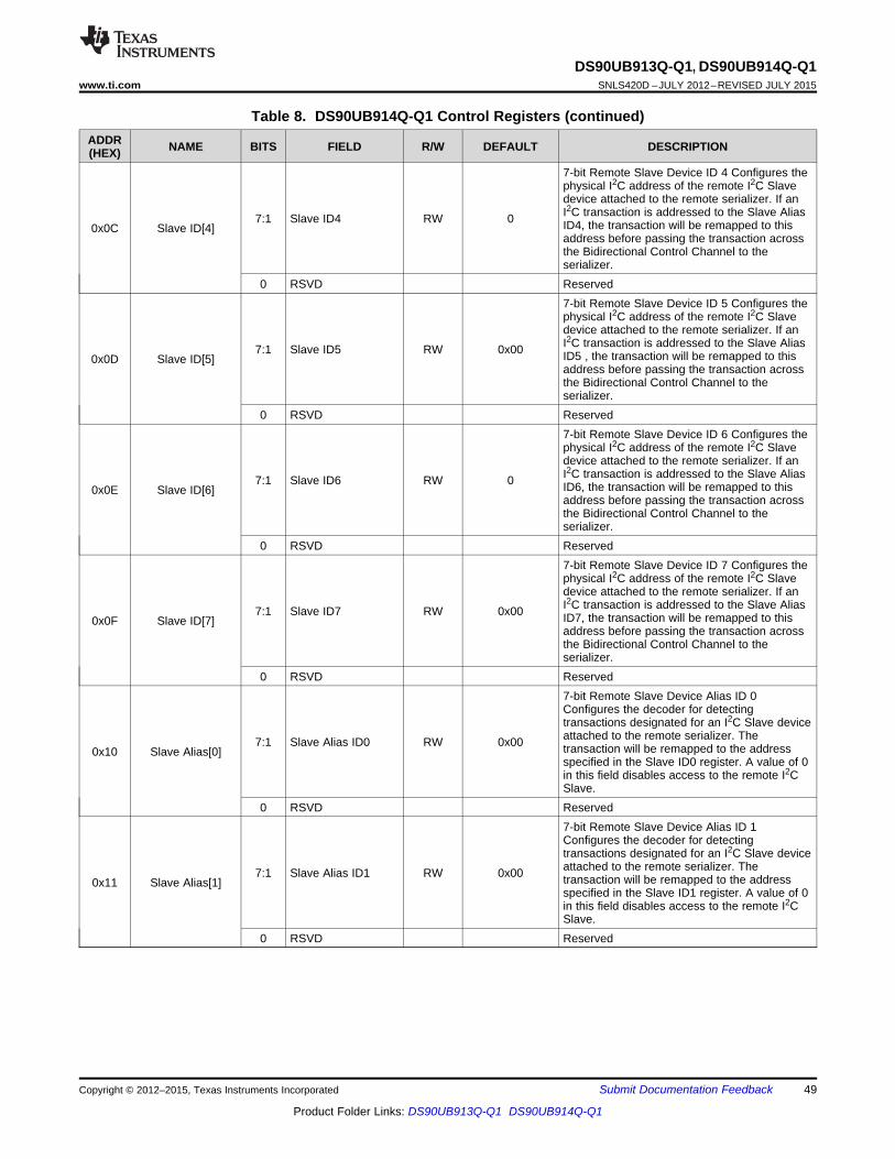
DS90UB913Q-Q1, DS90UB914Q-Q1www.ti.com SNLS420D –JULY 2012–REVISED JULY 2015
Table 8. DS90UB914Q-Q1 Control Registers (continued)ADDR NAME BITS FIELD R/W DEFAULT DESCRIPTION(HEX)
7-bit Remote Slave Device ID 4 Configures thephysical I2C address of the remote I2C Slavedevice attached to the remote serializer. If anI2C transaction is addressed to the Slave Alias7:1 Slave ID4 RW 0 ID4, the transaction will be remapped to this0x0C Slave ID[4]address before passing the transaction acrossthe Bidirectional Control Channel to theserializer.
0 RSVD Reserved7-bit Remote Slave Device ID 5 Configures thephysical I2C address of the remote I2C Slavedevice attached to the remote serializer. If anI2C transaction is addressed to the Slave Alias7:1 Slave ID5 RW 0x00 ID5 , the transaction will be remapped to this0x0D Slave ID[5]address before passing the transaction acrossthe Bidirectional Control Channel to theserializer.
0 RSVD Reserved7-bit Remote Slave Device ID 6 Configures thephysical I2C address of the remote I2C Slavedevice attached to the remote serializer. If anI2C transaction is addressed to the Slave Alias7:1 Slave ID6 RW 0 ID6, the transaction will be remapped to this0x0E Slave ID[6]address before passing the transaction acrossthe Bidirectional Control Channel to theserializer.
0 RSVD Reserved7-bit Remote Slave Device ID 7 Configures thephysical I2C address of the remote I2C Slavedevice attached to the remote serializer. If anI2C transaction is addressed to the Slave Alias7:1 Slave ID7 RW 0x00 ID7, the transaction will be remapped to this0x0F Slave ID[7]address before passing the transaction acrossthe Bidirectional Control Channel to theserializer.
0 RSVD Reserved7-bit Remote Slave Device Alias ID 0Configures the decoder for detectingtransactions designated for an I2C Slave deviceattached to the remote serializer. The7:1 Slave Alias ID0 RW 0x00 transaction will be remapped to the address0x10 Slave Alias[0]specified in the Slave ID0 register. A value of 0in this field disables access to the remote I2CSlave.
0 RSVD Reserved7-bit Remote Slave Device Alias ID 1Configures the decoder for detectingtransactions designated for an I2C Slave deviceattached to the remote serializer. The7:1 Slave Alias ID1 RW 0x00 transaction will be remapped to the address0x11 Slave Alias[1]specified in the Slave ID1 register. A value of 0in this field disables access to the remote I2CSlave.
0 RSVD Reserved
Copyright © 2012–2015, Texas Instruments Incorporated Submit Documentation Feedback 49
Product Folder Links: DS90UB913Q-Q1 DS90UB914Q-Q1

DS90UB913Q-Q1, DS90UB914Q-Q1SNLS420D –JULY 2012–REVISED JULY 2015 www.ti.com
Table 8. DS90UB914Q-Q1 Control Registers (continued)ADDR NAME BITS FIELD R/W DEFAULT DESCRIPTION(HEX)
7-bit Remote Slave Device Alias ID 2Configures the decoder for detectingtransactions designated for an I2C Slave deviceattached to the remote serializer. The7:1 Slave Alias ID2 RW 0x00 transaction will be remapped to the address0x12 Slave Alias[2]specified in the Slave ID2 register. A value of 0in this field disables access to the remote I2CSlave.
0 RSVD Reserved7-bit Remote Slave Device Alias ID 3Configures the decoder for detectingtransactions designated for an I2C Slave deviceattached to the remote serializer. The7:1 Slave Alias ID3 RW 0x00 transaction will be remapped to the address0x13 Slave Alias[3]specified in the Slave ID3 register. A value of 0in this field disables access to the remote I2CSlave.
0 RSVD Reserved7-bit Remote Slave Device Alias ID 4Configures the decoder for detectingtransactions designated for an I2C Slave deviceattached to the remote serializer. The7:1 Slave Alias ID4 RW 0x00 transaction will be remapped to the address0x14 Slave Alias[4]specified in the Slave ID4 register. A value of 0in this field disables access to the remote I2CSlave.
0 RSVD Reserved7-bit Remote Slave Device Alias ID 5Configures the decoder for detectingtransactions designated for an I2C Slave deviceattached to the remote serializer. The7:1 Slave Alias ID5 RW 0x00 transaction will be remapped to the address0x15 Slave Alias[5]specified in the Slave ID5 register. A value of 0in this field disables access to the remote I2CSlave.
0 RSVD Reserved7-bit Remote Slave Device Alias ID 6Configures the decoder for detectingtransactions designated for an I2C Slave deviceattached to the remote serializer. The7:1 Slave Alias ID6 RW 0x00 transaction will be remapped to the address0x16 Slave Alias[6]specified in the Slave ID6 register. A value of 0in this field disables access to the remote I2CSlave.
0 RSVD Reserved7-bit Remote Slave Device Alias ID 7Configures the decoder for detectingtransactions designated for an I2C Slave deviceattached to the remote serializer. The7:1 Slave Alias ID7 RW 0x00 transaction will be remapped to the address0x17 Slave Alias[7]specified in the Slave ID7 register. A value of 0in this field disables access to the remote I2CSlave.
0 RSVD ReservedParity errors threshold on the Forward channelduring normal information. This sets theParity Errors Parity Error0x18 7:0 RW 0 maximum number of parity errors that can beThreshold Threshold Byte 0 counted using register 0x1A.Least significant Byte.
50 Submit Documentation Feedback Copyright © 2012–2015, Texas Instruments Incorporated
Product Folder Links: DS90UB913Q-Q1 DS90UB914Q-Q1

DS90UB913Q-Q1, DS90UB914Q-Q1www.ti.com SNLS420D –JULY 2012–REVISED JULY 2015
Table 8. DS90UB914Q-Q1 Control Registers (continued)ADDR NAME BITS FIELD R/W DEFAULT DESCRIPTION(HEX)
Parity errors threshold on the Forward channelduring normal operation. This sets theParity Errors Parity Error0x19 7:0 RW 0 maximum number of parity errors that can beThreshold Threshold Byte 1 counted using register 0x1B.Most significant ByteNumber of parity errors in the Forward channel
0x1A Parity Errors 7:0 Parity Error Byte 0 RW 0 during normal operation.Least significant ByteNumber of parity errors in the Forward channel
0x1B Parity Errors 7:0 Parity Error Byte 1 RW 0 during normal operationMost significant ByteRevision ID7:4 Rev-ID R 0 0x0000: Production
3 RSVD ReservedParity Error detected
2 Parity Error R 0 1: Parity Errors detected0: No Parity Errors0x1C General Status
0 1: Serial input detected1 Signal Detect R 0: Serial input not detectedDeserializer CDR, PLL's clock to recoveredclock frequency0 Lock R 0 1: Deserializer locked to recovered clock0: Deserializer not locked
0 Local GPIO Output Value This value is the7 GPIO1 Output Vaue RW output on the GPIO pin when the GPIO function
is enabled, the local GPIO direction is Output.6 RSVD Reserved
GPIO1 Direction 1 Local GPIO Direction5 RW 1: InputGPIO[1] and0x1D 0: OutputGPIO[0] Config
GPIO Function Enable4 GPIO1 Enable RW 1 1: Enable GPIO operation
0: Enable normal operationLocal GPIO Output Value This value is output
3 GPIO0 Output Value RW 0 on the GPIO pin when the GPIO function isenabled, the local GPIO direction is Output.
2 RSVD ReservedLocal GPIO Direction
1 GPIO0 Direction RW 1 1: InputGPIO[1] and0x1D 0: OutputGPIO[0] ConfigGPIO Function Enable
0 GPIO0 Enable RW 1 1: Enable GPIO operation0: Enable normal operation
Copyright © 2012–2015, Texas Instruments Incorporated Submit Documentation Feedback 51
Product Folder Links: DS90UB913Q-Q1 DS90UB914Q-Q1
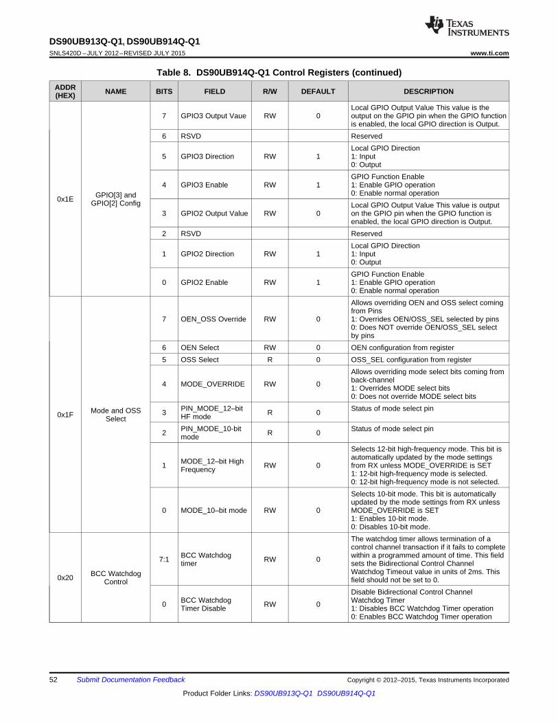
DS90UB913Q-Q1, DS90UB914Q-Q1SNLS420D –JULY 2012–REVISED JULY 2015 www.ti.com
Table 8. DS90UB914Q-Q1 Control Registers (continued)ADDR NAME BITS FIELD R/W DEFAULT DESCRIPTION(HEX)
Local GPIO Output Value This value is the7 GPIO3 Output Vaue RW 0 output on the GPIO pin when the GPIO function
is enabled, the local GPIO direction is Output.6 RSVD Reserved
Local GPIO Direction5 GPIO3 Direction RW 1 1: Input
0: OutputGPIO Function Enable
4 GPIO3 Enable RW 1 1: Enable GPIO operation0: Enable normal operationGPIO[3] and0x1E GPIO[2] Config Local GPIO Output Value This value is output
3 GPIO2 Output Value RW 0 on the GPIO pin when the GPIO function isenabled, the local GPIO direction is Output.
2 RSVD ReservedLocal GPIO Direction
1 GPIO2 Direction RW 1 1: Input0: OutputGPIO Function Enable
0 GPIO2 Enable RW 1 1: Enable GPIO operation0: Enable normal operationAllows overriding OEN and OSS select comingfrom Pins
7 OEN_OSS Override RW 0 1: Overrides OEN/OSS_SEL selected by pins0: Does NOT override OEN/OSS_SEL selectby pins
6 OEN Select RW 0 OEN configuration from register5 OSS Select R 0 OSS_SEL configuration from register
Allows overriding mode select bits coming fromback-channel4 MODE_OVERRIDE RW 0 1: Overrides MODE select bits0: Does not override MODE select bits
PIN_MODE_12–bit Status of mode select pinMode and OSS 3 R 00x1F HF modeSelectPIN_MODE_10-bit Status of mode select pin2 R 0mode
Selects 12-bit high-frequency mode. This bit isautomatically updated by the mode settingsMODE_12–bit High1 RW 0 from RX unless MODE_OVERRIDE is SETFrequency 1: 12-bit high-frequency mode is selected.0: 12-bit high-frequency mode is not selected.Selects 10-bit mode. This bit is automaticallyupdated by the mode settings from RX unless
0 MODE_10–bit mode RW 0 MODE_OVERRIDE is SET1: Enables 10-bit mode.0: Disables 10-bit mode.The watchdog timer allows termination of acontrol channel transaction if it fails to complete
BCC Watchdog within a programmed amount of time. This field7:1 RW 0timer sets the Bidirectional Control ChannelWatchdog Timeout value in units of 2ms. ThisBCC Watchdog0x20 field should not be set to 0.ControlDisable Bidirectional Control Channel
BCC Watchdog Watchdog Timer0 RW 0Timer Disable 1: Disables BCC Watchdog Timer operation0: Enables BCC Watchdog Timer operation
52 Submit Documentation Feedback Copyright © 2012–2015, Texas Instruments Incorporated
Product Folder Links: DS90UB913Q-Q1 DS90UB914Q-Q1

DS90UB913Q-Q1, DS90UB914Q-Q1www.ti.com SNLS420D –JULY 2012–REVISED JULY 2015
Table 8. DS90UB914Q-Q1 Control Registers (continued)ADDR NAME BITS FIELD R/W DEFAULT DESCRIPTION(HEX)
I2C Pass-Through All Transactions7 I2C pass-through all RW 0 0: Disabled
1: EnabledInternal SDA Hold Time This field configuresthe amount of internal hold time provided for0x21 I2C Control 1 6:4 I2C SDA Hold RW 0 the SDA input relative to the SCL input. Unitsare 50ns.I2C Glitch Filter Depth This field configures the
3:0 I2C Filter Depth RW 0 maximum width of glitch pulses on the SCL andSDA inputs that will be rejected. Units are 10ns.Control Channel Sequence Error Detected Thisbit indicates a sequence error has beendetected in forward control channel.Forward Channel7 R 0 1: If this bit is set, an error may have occurredSequence Error in the control channel operation0: No forward channel errors have beendetected on the control channel
Clear Sequence Clears the Sequence Error Detect bit6 RW 0Error5 RSVD Reserved
SDA Output Delay This field configures outputdelay on the SDA output. Setting this value willincrease output delay in units of 50 ns. Nominaloutput delay values for SCL to SDA are:4:3 SDA Output Delay RW 0 00 : 350ns01: 400ns10: 450ns11: 500nsDisable Remote Writes to local registers0x22 I2C Control 2 Setting this bit to a 1 will prevent remote writesto local device registers from across the control
2 Local Write Disable RW 0 channel. This prevents writes to the deserializerregisters from an I2C master attached to theserializer. Setting this bit does not affect remoteaccess to I2C slaves at the deserializer.Speed up I2C Bus Watchdog Timer1: Watchdog Timer expires after approximatelyI2C Bus Timer1 RW 0 50 µsSpeed up 0: Watchdog Timer expires after approximately1 s.Disable I2C Bus Watchdog Timer When the I2CWatchdog Timer may be used to detect whenthe I2C bus is free or hung up following aninvalid termination of a transaction. If SDA isI2C Bus Timer0 RW 0 high and no signaling occurs for approximatelyDisable 1 second, the I2C bus will assumed to be free.If SDA is low and no signaling occurs, thedevice will attempt to clear the bus by driving 9clocks on SCL
General-Purpose Scratch Register0x23 7:0 GPCR RW 0Control7:4 RSVD Reserved
Bist Configured through Pin.BIST Pin 1: Bist configured through pin.3 RW 1Configuration 0: Bist configured through register bit
"reg_24[0]"0x24 BIST Control
BIST Clock Source2:1 BIST Clock Source RW 00 See Table 10BIST Control
0 BIST Enable RW 0 1: Enabled0: Disabled
Copyright © 2012–2015, Texas Instruments Incorporated Submit Documentation Feedback 53
Product Folder Links: DS90UB913Q-Q1 DS90UB914Q-Q1

DS90UB913Q-Q1, DS90UB914Q-Q1SNLS420D –JULY 2012–REVISED JULY 2015 www.ti.com
Table 8. DS90UB914Q-Q1 Control Registers (continued)ADDR NAME BITS FIELD R/W DEFAULT DESCRIPTION(HEX)
Number of Forward channel Parity errors in the0x25 Parity Error Count 7:0 BIST Error Count R 0 BIST mode.0x26 - RESERVED0x3B
7:2 RSVD ReservedSelects the divider for the OSC clock out onPCLK when system is not locked and selectedOscillator output0x3C OSC OUT DIVIDER by OEN/OSSSEL 0x02[5]divider select 1:0 RW 0SEL 00: 50M (± 30%)01: 25M (± 30%)1X: 12.5M (± 30%)
0x3D - RESERVED0x3E7:5 RSVD Reserved
CML Output 0: CML Loop-through Driver is powered up0x3F 4 CML OUT Enable RW 1Enable 1: CML Loop-through Driver is powered down.3:0 RSVD Reserved
I2C Master SCL High Time This field configuresthe high pulse width of the SCL output whenthe deserializer is the Master on the local I2Cbus. Units are 50 ns for the nominal oscillator
0x40 SCL High Time 7:0 SCL High Time RW 0x82 clock frequency. The default value is set toprovide a minimum (4μs + 0.3μs of rise time forcases where rise time is very fast) SCL hightime with the internal oscillator clock running at26MHz rather than the nominal 20MHz.I2C SCL Low Time This field configures the lowpulse width of the SCL output when thedeserializer is the Master on the local I2C bus.This value is also used as the SDA setup timeby the I2C Slave for providing data prior toreleasing SCL during accesses over the
0x41 SCL Low Time 7:0 SCL Low Time RW 0x82 Bidirectional Control Channel. Units are 50 nsfor the nominal oscillator clock frequency. Thedefault value is set to provide a minimum(4.7µs + 0.3µs of fall time for cases where falltime is very fast) SCL low time with the internaloscillator clock running at 26MHz rather thanthe nominal 20MHz.
7:2 RSVD Reserved1: This bit introduces multiple errors into BackForce Back Channel1 RW 0 channel frame.Error0x42 CRC Force Error 0: No effect1: This bit introduces ONLY one error into BackForce One Back0 RW 0 channel frame. Self clearing bitChannel Error 0: No effect
0x43 - RESERVED0x4C7 RSVD Reserved
AEQ Test Mode Bypass AEQ and use set manual EQ value0x4D 6 AEQ Bypass RW 0Select using register 0x045:0 RSVD Reserved
AEQ / Manual Eq Read back the adaptive and manual0x4E EQ Value 7:0 R 0Readback Equalization value
54 Submit Documentation Feedback Copyright © 2012–2015, Texas Instruments Incorporated
Product Folder Links: DS90UB913Q-Q1 DS90UB914Q-Q1

DS90UB913Q-Q1, DS90UB914Q-Q1www.ti.com SNLS420D –JULY 2012–REVISED JULY 2015
Table 9. Clock Sources for Forward Channel Frame on the Serializer During Normal OperationDS90UB913Q 10-BIT 12-BIT 12-BIT
REG 0x14 [2:1] MODE HIGH-FREQUENCY MODE LOW-FREQUENCY MODE00 50 MHz 37.5 MHz 25 MHz01 100 MHz 75 MHz 50 MHz10 50 MHz 37.5 MHz 25 MHz11 25MHz 18.75 MHz 12.5 MHz
Table 10. BIST Clock SourcesDS90UB914Q 10-BIT 12-BIT 12-BIT
REG 0x24 [2:1] MODE HIGH-FREQUENCY MODE LOW-FREQUENCY MODE00 PCLK PCLK PCLK01 100 MHz 75 MHz 50 MHz10 50 MHz 37.5 MHz 25 MHz11 25MHz 18.75 MHz 12.5 MHz
Copyright © 2012–2015, Texas Instruments Incorporated Submit Documentation Feedback 55
Product Folder Links: DS90UB913Q-Q1 DS90UB914Q-Q1

FPD-Link III
Bi-DirectionalControl Channel
Image Sensor
ECU Module
DIN[11:0] or DIN[9:0]HSYNC, VSYNC
SDA
SCL
DOUT- RIN-
DOUT+ RIN+
Camera Unit
10 or 12
DATA
HSYNC
VSYNC
PCLKPixel Clock
SDA
SCL
Microcontroller
ROUT[11:0] or
ROUT[9:0] HSYNC, VSYNC
SDA
SCL
PCLK
10 or 12
DATA
HSYNC
VSYNC
Pixel Clock
SDA
SCL
Camera Data
DS90UB914QDeserializer
DS90UB913QSerializer
GPO[3:0]GPO[3:0]
4
GPIO[3:0]
4GPIO[3:0]
Camera Data
DOUT-
DOUT+
D
RIN-
RIN+
R
DS90UB913Q-Q1, DS90UB914Q-Q1SNLS420D –JULY 2012–REVISED JULY 2015 www.ti.com
11 Application and Implementation
NOTEInformation in the following applications sections is not part of the TI componentspecification, and TI does not warrant its accuracy or completeness. TI’s customers areresponsible for determining suitability of components for their purposes. Customers shouldvalidate and test their design implementation to confirm system functionality.
11.1 Applications InformationThe serializer and deserializer support only AC-coupled interconnects through an integrated DC-balanceddecoding scheme. External AC-coupling capacitors must be placed in series in the FPD-Link III signal path asillustrated in Figure 45.
Figure 45. AC-Coupled Connection
For high-speed FPD-Link III transmissions, the smallest available package should be used for the AC-couplingcapacitor. This will help minimize degradation of signal quality due to package parasitics. The I/Os require a100-nF AC-coupling capacitors to the line.
11.2 Typical Application
Figure 46. Application Block Diagram
11.2.1 Design Requirements
11.2.1.1 Transmission MediaThe DS90UB91xQ-Q1 chipset is intended to be used in a point-to-point configuration through a shielded twistedpair cable. The serializer and deserializer provide internal termination to minimize impedance discontinuities. Theinterconnect (cable and connectors) should have a differential impedance of 100 Ω. The maximum length ofcable that can be used is dependent on the quality of the cable (gauge, impedance), connector, board(discontinuities, power plane), the electrical environment (for example, power stability, ground noise, input clockjitter, PCLK frequency, and so forth). The resulting signal quality at the receiving end of the transmission mediamay be assessed by monitoring the differential eye opening of the serial data stream. A differential probe shouldbe used to measure across the termination resistor at the CMLOUTP/N pins. Figure 20 illustrates the minimumeye width and eye height that is necessary for bit error free operation.
56 Submit Documentation Feedback Copyright © 2012–2015, Texas Instruments Incorporated
Product Folder Links: DS90UB913Q-Q1 DS90UB914Q-Q1

DIN0DIN1DIN2DIN3DIN4DIN5DIN6
DIN7DIN8DIN9DIN10DIN11HSVSPCLK
PDB
DOUT+DOUT-
VDDCML
DAP (GND)
VDDPLL
VDDT
1.8VDS90UB913Q (SER)
C4
C5 C10
C11
C1
C2
NOTE:C1 - C2 = 0.1 PF (50 WV)C3 ± C7 = 0.01 PFC8 - C12 = 0.1 PFC13 - C14 = 4.7 PFC15 = 22 PFC16 - C17 = >100 pF RPU = 1 k: to 4.7 k:RID (see ID[x] Resistor Value Table)FB1 - FB4: Impedance = 1 k: (@ 100 MHz) low DC resistance (<1:)
The "Optional" components shown are provisions to provide higher system noise immunity and will therefore result in higher performance.
LVCMOSParallel
Bus
SerialFPD-Link IIIInterface
MODE
ID[X]
VDDIO
RES
C8
LVCMOSControl
Interface
VDDIO
1.8V
RID
10 k:
C13C3
FB1
FB2
VDDDC7
SCL
VDDIO
C17
RPU
C16
RPU
SDA
I2CBus
InterfaceFB3
FB4
GPO[1]GPO[0]GPO
ControlInterface
C6
Optional
Optional
GPO[3]GPO[2]
C9
1.8V
C12
1.8V
C15
C141.8V
1.8V
RID
10 k:
DS90UB913Q-Q1, DS90UB914Q-Q1www.ti.com SNLS420D –JULY 2012–REVISED JULY 2015
Typical Application (continued)11.2.1.2 Adaptive Equalizer – Loss CompensationThe adaptive equalizer is designed to compensate for signal degradation due to the differential insertion loss ofthe interconnect components. There are limits to the amount of loss that can be compensated – these limits aredefined by the gain curve of the equalizer. In addition, there is an inherent tolerance for loss defined by the deltabetween the minimum VDO of the serializer and the input threshold (Vswing) of the deserializer. In order todetermine the maximum cable reach, other factors that affect signal integrity such as jitter, skew, ISI, crosstalk,and so forth, need to be taken into consideration. Figure 49 illustrates the maximum allowable interconnect losswith the adaptive equalizer at its maximum gain setting (914 equalizer gain).
11.2.2 Detailed Design ProcedureFigure 47 shows the typical connection of a DS90UB913Q-Q1 serializer.
Figure 47. DS90UB913Q-Q1 Typical Connection Diagram — Pin Control
Copyright © 2012–2015, Texas Instruments Incorporated Submit Documentation Feedback 57
Product Folder Links: DS90UB913Q-Q1 DS90UB914Q-Q1

ROUT0ROUT1ROUT2ROUT3ROUT4ROUT5ROUT6
ROUT7ROUT8ROUT9
ROUT10ROUT11
HSVS
PDB
DAP (GND)
RIN1+
RIN1-
VDDR
VDDIO3
VDDIO1
VDDIO2
VDDIODS90UB914Q (Des)
C9
C10
C1
C2
VDDD
MODE
RES_PIN43
C12
1.8V
SerialFPD-Link II
Interface
PCLK
LOCK
C8
C14 C17
C15 C19
VDDPLL
VDDCML
VDDSSCG
NOTE:C1 - C2 = 0.1 PF (50 WV)C3 - C10 = 0.01 PFC11 - C16 = 0.1 PFC17 - C18 = 4.7 PFC19 = 22 PFC20 - C21 = >100 pFRPU = 1 k: to 4.7 k:RID (see ID[x] Resistor Value Table)FB1 - FB4: Impedance = 1 k: (@ 100 MHz) low DC resistance (<1:)
The "Optional" components shown are provisions to provide higher system noise immunity and will therefore result in higher performance.
C3 C11 C18C16
FB1
FB2
SCL
VDDIO
C21
RPU
C20
RPU
SDA
I2CBus
InterfaceFB3
FB4
IDx[0]
1.8V
RID0
10 k:
Optional
Optional
LVCMOSParallel Outputs
C4
C13C5
1.8V
1.8V
C6
C7
RIN0+
RIN0-C1
C2
IDx[1]
RID1
10 k:
PASS
1.8V
RMODE
10 k:
1.8V
SELOEN
OSS_SELBISTEN
GPIO[0]GPIO[1]GPIO[2]
GPIO[3]
DS90UB913Q-Q1, DS90UB914Q-Q1SNLS420D –JULY 2012–REVISED JULY 2015 www.ti.com
Typical Application (continued)Figure 48 shows a typical connection of the DS90UB914Q-Q1 deserializer.
Figure 48. DS90UB914Q-Q1 Typical Connection Diagram — Pin Control
58 Submit Documentation Feedback Copyright © 2012–2015, Texas Instruments Incorporated
Product Folder Links: DS90UB913Q-Q1 DS90UB914Q-Q1

200 300 400 500 600 700
SERIAL LINE FREQUENCY (MHz)
0
5
10
15
20
25
EF
FE
CT
IVE
GA
IN (
dB)
100
VOD-Vswing Loss
914 Equalizer Gain (dB)
Allowable InterconnectLoss
DS90UB913Q-Q1, DS90UB914Q-Q1www.ti.com SNLS420D –JULY 2012–REVISED JULY 2015
Typical Application (continued)11.2.3 Application Curve
Figure 49. Adaptive Equalizer – Interconnect Loss Compensation
Copyright © 2012–2015, Texas Instruments Incorporated Submit Documentation Feedback 59
Product Folder Links: DS90UB913Q-Q1 DS90UB914Q-Q1

DS90UB913Q-Q1, DS90UB914Q-Q1SNLS420D –JULY 2012–REVISED JULY 2015 www.ti.com
12 Power Supply RecommendationsThis device is designed to operate from an input core voltage supply of 1.8 V. Some devices provide separatepower and ground terminals for different portions of the circuit. This is done to isolate switching noise effectsbetween different sections of the circuit. Separate planes on the PCB are typically not required. Terminaldescription tables typically provide guidance on which circuit blocks are connected to which power terminal pairs.In some cases, an external filter may be used to provide clean power to sensitive circuits such as PLLs.
13 Layout
13.1 Layout GuidelinesPrinted-circuit-board layout and stack-up for the serializer and deserializer devices should be designed to providelow-noise power feed to the device. Good layout practice will also separate high frequency or high-level inputsand outputs to minimize unwanted stray noise pickup, feedback and interference. Power system performancemay be greatly improved by using thin dielectrics (2 to 4 mils) for power/ground sandwiches. This arrangementprovides plane capacitance for the PCB power system with low-inductance parasitics, which has provenespecially effective at high frequencies, and makes the value and placement of external bypass capacitors lesscritical. External bypass capacitors should include both RF ceramic and tantalum electrolytic types. RF capacitorsmay use values in the range of 0.01 µF to 0.1 µF. Tantalum capacitors may be in the 2.2-µF to 10-µF range.Voltage rating of the tantalum capacitors should be at least 5× the power supply voltage being used.
Surface mount capacitors are recommended due to their smaller parasitics. When using multiple capacitors persupply pin, locate the smaller value closer to the pin. A large bulk capacitor is recommend at the point of powerentry. This is typically in the 50-µF to 100-µF range and will smooth low frequency switching noise. It isrecommended to connect power and ground pins directly to the power and ground planes with bypass capacitorsconnected to the plane with a via on both ends of the capacitor. Connecting power or ground pins to an externalbypass capacitor will increase the inductance of the path.
A small body size X7R chip capacitor, such as 0603, is recommended for external bypass. Its small body sizereduces the parasitic inductance of the capacitor. The user must pay attention to the resonance frequency ofthese external bypass capacitors, usually in the range of 20 to 30 MHz. To provide effective bypassing, multiplecapacitors are often used to achieve low impedance between the supply rails over the frequency of interest. Athigh frequency, it is also a common practice to use two vias from power and ground pins to the planes, reducingthe impedance at high frequency.
Some devices provide separate power for different portions of the circuit. This is done to isolate switching noiseeffects between different sections of the circuit. Separate planes on the PCB are typically not required. Pindescription tables typically provide guidance on which circuit blocks are connected to which power pin pairs. Insome cases, an external filter many be used to provide clean power to sensitive circuits such as PLLs.
Use at least a four-layer board with a power and ground plane. Locate LVCMOS signals away from thedifferential lines to prevent coupling from the LVCMOS lines to the differential lines. Closely-coupled differentiallines of 100 Ω are typically recommended for differential interconnect. The closely coupled lines help to ensurethat coupled noise will appear as common-mode and thus is rejected by the receivers. The tightly coupled lineswill also radiate less.
Information on the WQFN style package is provided in Texas Instruments' Application Note: AN-1187(SNOA401).
See AN-1108 (SNLA008) and AN-905 (SNLA035) for full details.• Use 100-Ω coupled differential pairs• Use the S, 2S, and 3S rule in spacings
– S = space between the pair– 2S = space between pairs– 3S = space to LVCMOS signal
• Minimize the number of Vias• Use differential connectors when operating above 500Mbps line speed• Maintain balance of the traces• Minimize skew within the pair
60 Submit Documentation Feedback Copyright © 2012–2015, Texas Instruments Incorporated
Product Folder Links: DS90UB913Q-Q1 DS90UB914Q-Q1

DS90UB913Q-Q1, DS90UB914Q-Q1www.ti.com SNLS420D –JULY 2012–REVISED JULY 2015
Layout Guidelines (continued)Additional general guidance can be found in the LVDS Owner’s Manual - available in PDF format from the TexasInstrument web site at: www.ti.com/lvds
13.2 Layout ExampleStencil parameters such as aperture area ratio and the fabrication process have a significant impact on pastedeposition. Inspection of the stencil prior to placement of the WQFN package is highly recommended to improveboard assembly yields. If the via and aperture openings are not carefully monitored, the solder may flowunevenly through the DAP. Stencil parameters for aperture opening and via locations are shown in Figure 50.
Figure 50. No Pullback WQFN, Single Row Reference Diagram
Figure 50 and Figure 51 PCB layout examples are derived from the layout design of the DS90UB913Q-Q1Serializer and DS90UB914Q-Q1 Deserializer Evaluation Kit (SNLU110). These graphics and additional layoutdescription are used to demonstrate both proper routing and proper solder techniques when designing in theserializer and deserializer.
Table 11. No Pullback WQFN Stencil Aperture Summary for DS90UB913Q-Q1 and DS90UB914Q-Q1GAPSTENCIL NUMBER OFPCB I/O PAD PCB PCB DAP STENCIL I/O BETWEENPIN DAP DAPDEVICE MKT DWG SIZE PITCH SIZE APERTURE DAPCOUNT APERTURE APERTURE(mm) (mm) (mm) (mm) APERTURE(mm) OPENINGS (Dim A mm)
DS90UB913Q-Q1 32 RTV 0.25 x 0.6 0.5 3.1 x 3.1 0.25 x 0.7 1.4 x 1.4 4 0.2
DS90UB914Q-Q1 48 RHS 0.25 x 0.6 0.5 5.1 x 5.1 0.25 x 0.7 1.1 x 1.1 16 0.2
Copyright © 2012–2015, Texas Instruments Incorporated Submit Documentation Feedback 61
Product Folder Links: DS90UB913Q-Q1 DS90UB914Q-Q1

DS90UB913Q-Q1, DS90UB914Q-Q1SNLS420D –JULY 2012–REVISED JULY 2015 www.ti.com
Figure 51. 48-Pin WQFN Stencil Example of Via and Opening Placement
62 Submit Documentation Feedback Copyright © 2012–2015, Texas Instruments Incorporated
Product Folder Links: DS90UB913Q-Q1 DS90UB914Q-Q1

DS90UB913Q-Q1, DS90UB914Q-Q1www.ti.com SNLS420D –JULY 2012–REVISED JULY 2015
14 Device and Documentation Support
14.1 Documentation Support
14.1.1 Related DocumentationFor related documentation, see the following:• Absolute Maximum Ratings for Soldering, SNOA549• AN-1187 Leadless Leadframe Package (LLP), SN0A401• AN-1108 Channel-Link PCB and Interconnect Design-In Guidelines, SNLA008• Transmission Line RAPIDESIGNER Operation and Applications Guide, SNLA035• DS90UB913Q-Q1 Serializer and DS90UB914Q-Q1 Deserializer Evaluation Kit, SNLU110
14.2 Related LinksThe table below lists quick access links. Categories include technical documents, support and communityresources, tools and software, and quick access to sample or buy.
Table 12. Related LinksTECHNICAL TOOLS & SUPPORT &PARTS PRODUCT FOLDER SAMPLE & BUY DOCUMENTS SOFTWARE COMMUNITY
DS90UB913Q-Q1 Click here Click here Click here Click here Click hereDS90UB914Q-Q1 Click here Click here Click here Click here Click here
14.3 Community ResourcesThe following links connect to TI community resources. Linked contents are provided "AS IS" by the respectivecontributors. They do not constitute TI specifications and do not necessarily reflect TI's views; see TI's Terms ofUse.
TI E2E™ Online Community TI's Engineer-to-Engineer (E2E) Community. Created to foster collaborationamong engineers. At e2e.ti.com, you can ask questions, share knowledge, explore ideas and helpsolve problems with fellow engineers.
Design Support TI's Design Support Quickly find helpful E2E forums along with design support tools andcontact information for technical support.
14.4 TrademarksE2E is a trademark of Texas Instruments.All other trademarks are the property of their respective owners.
14.5 Electrostatic Discharge CautionThese devices have limited built-in ESD protection. The leads should be shorted together or the device placed in conductive foamduring storage or handling to prevent electrostatic damage to the MOS gates.
14.6 GlossarySLYZ022 — TI Glossary.
This glossary lists and explains terms, acronyms, and definitions.
15 Mechanical, Packaging, and Orderable InformationThe following pages include mechanical, packaging, and orderable information. This information is the mostcurrent data available for the designated devices. This data is subject to change without notice and revision ofthis document. For browser-based versions of this data sheet, refer to the left-hand navigation.
Copyright © 2012–2015, Texas Instruments Incorporated Submit Documentation Feedback 63
Product Folder Links: DS90UB913Q-Q1 DS90UB914Q-Q1

PACKAGE OPTION ADDENDUM
www.ti.com 10-Dec-2020
Addendum-Page 1
PACKAGING INFORMATION
Orderable Device Status(1)
Package Type PackageDrawing
Pins PackageQty
Eco Plan(2)
Lead finish/Ball material
(6)
MSL Peak Temp(3)
Op Temp (°C) Device Marking(4/5)
Samples
DS90UB913QSQ/NOPB ACTIVE WQFN RTV 32 1000 RoHS & Green SN Level-3-260C-168 HR -40 to 105 UB913SQ
DS90UB913QSQE/NOPB ACTIVE WQFN RTV 32 250 RoHS & Green SN Level-3-260C-168 HR -40 to 105 UB913SQ
DS90UB913QSQX/NOPB ACTIVE WQFN RTV 32 4500 RoHS & Green SN Level-3-260C-168 HR -40 to 105 UB913SQ
DS90UB914QSQ/NOPB ACTIVE WQFN RHS 48 1000 RoHS & Green SN Level-3-260C-168 HR -40 to 105 UB914QSQ
DS90UB914QSQE/NOPB ACTIVE WQFN RHS 48 250 RoHS & Green SN Level-3-260C-168 HR -40 to 105 UB914QSQ
DS90UB914QSQX/NOPB ACTIVE WQFN RHS 48 2500 RoHS & Green SN Level-3-260C-168 HR -40 to 105 UB914QSQ
(1) The marketing status values are defined as follows:ACTIVE: Product device recommended for new designs.LIFEBUY: TI has announced that the device will be discontinued, and a lifetime-buy period is in effect.NRND: Not recommended for new designs. Device is in production to support existing customers, but TI does not recommend using this part in a new design.PREVIEW: Device has been announced but is not in production. Samples may or may not be available.OBSOLETE: TI has discontinued the production of the device.
(2) RoHS: TI defines "RoHS" to mean semiconductor products that are compliant with the current EU RoHS requirements for all 10 RoHS substances, including the requirement that RoHS substancedo not exceed 0.1% by weight in homogeneous materials. Where designed to be soldered at high temperatures, "RoHS" products are suitable for use in specified lead-free processes. TI mayreference these types of products as "Pb-Free".RoHS Exempt: TI defines "RoHS Exempt" to mean products that contain lead but are compliant with EU RoHS pursuant to a specific EU RoHS exemption.Green: TI defines "Green" to mean the content of Chlorine (Cl) and Bromine (Br) based flame retardants meet JS709B low halogen requirements of <=1000ppm threshold. Antimony trioxide basedflame retardants must also meet the <=1000ppm threshold requirement.
(3) MSL, Peak Temp. - The Moisture Sensitivity Level rating according to the JEDEC industry standard classifications, and peak solder temperature.
(4) There may be additional marking, which relates to the logo, the lot trace code information, or the environmental category on the device.
(5) Multiple Device Markings will be inside parentheses. Only one Device Marking contained in parentheses and separated by a "~" will appear on a device. If a line is indented then it is a continuationof the previous line and the two combined represent the entire Device Marking for that device.
(6) Lead finish/Ball material - Orderable Devices may have multiple material finish options. Finish options are separated by a vertical ruled line. Lead finish/Ball material values may wrap to twolines if the finish value exceeds the maximum column width.

PACKAGE OPTION ADDENDUM
www.ti.com 10-Dec-2020
Addendum-Page 2
Important Information and Disclaimer:The information provided on this page represents TI's knowledge and belief as of the date that it is provided. TI bases its knowledge and belief on informationprovided by third parties, and makes no representation or warranty as to the accuracy of such information. Efforts are underway to better integrate information from third parties. TI has taken andcontinues to take reasonable steps to provide representative and accurate information but may not have conducted destructive testing or chemical analysis on incoming materials and chemicals.TI and TI suppliers consider certain information to be proprietary, and thus CAS numbers and other limited information may not be available for release.
In no event shall TI's liability arising out of such information exceed the total purchase price of the TI part(s) at issue in this document sold by TI to Customer on an annual basis.

TAPE AND REEL INFORMATION
*All dimensions are nominal
Device PackageType
PackageDrawing
Pins SPQ ReelDiameter
(mm)
ReelWidth
W1 (mm)
A0(mm)
B0(mm)
K0(mm)
P1(mm)
W(mm)
Pin1Quadrant
DS90UB913QSQ/NOPB WQFN RTV 32 1000 178.0 12.4 5.3 5.3 1.3 8.0 12.0 Q1
DS90UB913QSQE/NOPB WQFN RTV 32 250 178.0 12.4 5.3 5.3 1.3 8.0 12.0 Q1
DS90UB913QSQX/NOPB WQFN RTV 32 4500 330.0 12.4 5.3 5.3 1.3 8.0 12.0 Q1
DS90UB914QSQ/NOPB WQFN RHS 48 1000 330.0 16.4 7.3 7.3 1.3 12.0 16.0 Q1
DS90UB914QSQE/NOPB WQFN RHS 48 250 178.0 16.4 7.3 7.3 1.3 12.0 16.0 Q1
DS90UB914QSQX/NOPB WQFN RHS 48 2500 330.0 16.4 7.3 7.3 1.3 12.0 16.0 Q1
PACKAGE MATERIALS INFORMATION
www.ti.com 5-Nov-2021
Pack Materials-Page 1

*All dimensions are nominal
Device Package Type Package Drawing Pins SPQ Length (mm) Width (mm) Height (mm)
DS90UB913QSQ/NOPB WQFN RTV 32 1000 208.0 191.0 35.0
DS90UB913QSQE/NOPB WQFN RTV 32 250 208.0 191.0 35.0
DS90UB913QSQX/NOPB WQFN RTV 32 4500 853.0 449.0 35.0
DS90UB914QSQ/NOPB WQFN RHS 48 1000 853.0 449.0 35.0
DS90UB914QSQE/NOPB WQFN RHS 48 250 208.0 191.0 35.0
DS90UB914QSQX/NOPB WQFN RHS 48 2500 853.0 449.0 35.0
PACKAGE MATERIALS INFORMATION
www.ti.com 5-Nov-2021
Pack Materials-Page 2


IMPORTANT NOTICE AND DISCLAIMERTI PROVIDES TECHNICAL AND RELIABILITY DATA (INCLUDING DATA SHEETS), DESIGN RESOURCES (INCLUDING REFERENCE DESIGNS), APPLICATION OR OTHER DESIGN ADVICE, WEB TOOLS, SAFETY INFORMATION, AND OTHER RESOURCES “AS IS” AND WITH ALL FAULTS, AND DISCLAIMS ALL WARRANTIES, EXPRESS AND IMPLIED, INCLUDING WITHOUT LIMITATION ANY IMPLIED WARRANTIES OF MERCHANTABILITY, FITNESS FOR A PARTICULAR PURPOSE OR NON-INFRINGEMENT OF THIRD PARTY INTELLECTUAL PROPERTY RIGHTS.These resources are intended for skilled developers designing with TI products. You are solely responsible for (1) selecting the appropriate TI products for your application, (2) designing, validating and testing your application, and (3) ensuring your application meets applicable standards, and any other safety, security, regulatory or other requirements.These resources are subject to change without notice. TI grants you permission to use these resources only for development of an application that uses the TI products described in the resource. Other reproduction and display of these resources is prohibited. No license is granted to any other TI intellectual property right or to any third party intellectual property right. TI disclaims responsibility for, and you will fully indemnify TI and its representatives against, any claims, damages, costs, losses, and liabilities arising out of your use of these resources.TI’s products are provided subject to TI’s Terms of Sale or other applicable terms available either on ti.com or provided in conjunction with such TI products. TI’s provision of these resources does not expand or otherwise alter TI’s applicable warranties or warranty disclaimers for TI products.TI objects to and rejects any additional or different terms you may have proposed. IMPORTANT NOTICE
Mailing Address: Texas Instruments, Post Office Box 655303, Dallas, Texas 75265Copyright © 2021, Texas Instruments Incorporated


![PVCPR11 Edital 3.5 GHz v03.ppt [Modo de Compatibilidade]...2011/06/09 · 35 MHz 35 MHz 10 MHz 10 MHz 10 MHz 10 MHz 10 MHz 10 MHz 3.400,00 MHz 3.600,00 MHz 10 MHz 35 MHz 10 MHz 10](https://img.dokumen.tips/doc/110x75/5f7286506e7f433bb4685297/pvcpr11-edital-35-ghz-v03ppt-modo-de-compatibilidade-20110609-35-mhz.jpg)