Embed Size (px)
Citation preview

Typical Operating Circuit appears at end of data sheet.
General DescriptionThe DS3882 is a dual-channel cold-cathode fluorescent lamp (CCFL) controller for applications that provide up to 300:1 dimming. It is ideal for driving CCFLs used to backlight liquid crystal displays (LCDs) in navigation and infotainment applications and for driving CCFLs used to backlight instrument clusters. The DS3882 is also appro-priate for use in marine and aviation applications.The DS3882 features EMI suppression functionality and provides a lamp current overdrive mode for rapid lamp heating in cold weather conditions. The DS3882 supports configurations of 1 or 2 lamps with fully independent lamp control and minimal external components. Multiple DS3882 controllers can be cascaded to support applications requir-ing more than 2 lamps. Control of the DS3882, after initial programming setup, can be completely achieved through I2C software communication. Many DS3882 functions are also pin-controllable if software control is not desired.
Applications ● Instrument Clusters ● Marine and Aviation LCDs
Features ● Dual-Channel CCFL Controllers for Backlighting
LCD Panels and Instrument Clusters in Navigation/Infotainment Applications
● Minimal External Components Required ● I2C Interface ● Per-Channel Lamp-Fault Monitoring for Lamp-Open,
Lamp-Overcurrent, Failure to Strike, and Overvoltage Conditions
● Status Register Reports Fault Conditions ● Accurate (±5%) Independent On-Board Oscillators
for Lamp Frequency (40kHz to 100kHz) and DPWM Burst-Dimming Frequency (22.5Hz to 440Hz)
● Lamp and DPWM Frequencies can be Synchronized with External Sources to Reduce Visual LCD Artifacts in Video Applications
● Optional Spread-Spectrum Lamp Clock Reduces EMI ● Lamp Frequency can be Stepped Up or Down to
Move EMI Spurs Out of Band ● Lamp Current Overdrive Mode with Automatic
Turn-Off Quickly Warms Lamp in Cold Temperatures ● Analog and Digital Brightness Control ● 300:1 Dimming Range Possible Using the Digital
Brightness Control Option ● Programmable Soft-Start Minimizes Audible
Transformer Noise ● On-Board Nonvolatile (NV) Memory Allows Device
Customization ● 8-Byte NV User Memory for Storage of Serial
Numbers and Date Codes ● Low-Power Standby Mode ● 4.75V to 5.25V Single-Supply Operation ● -40°C to +105°C Temperature Range ● 28-Pin TSSOP Package
+Denotes a lead(Pb)-free/RoHS-compliant package.T&R = Tape and reel.
PART TEMP RANGE PIN-PACKAGEDS3882E+C -40°C to +105°C 28 TSSOP
DS3882E+T&R/C -40°C to +105°C 28 TSSOP
28
27
26
25
24
23
22
1
2
3
4
5
6
7
OVD2
LCM2
GB2
GA2SCL
SDA
A0
FAULT
TOP VIEW
VCC
PDN
LCOBRIGHT
LOSC
218 GNDPSYNC
209 STEPPOSC
1910 N.C.A1
1811 OVD1GND_S
1712 LCM1SVML
1613 GB1SVMH
1514 GA1VCC
LSYNC
TSSOP
DS3882
+
DS3882 Dual-Channel CCFL Controller
19-5666; Rev 2; 12/10
Ordering Information
Pin Configuration
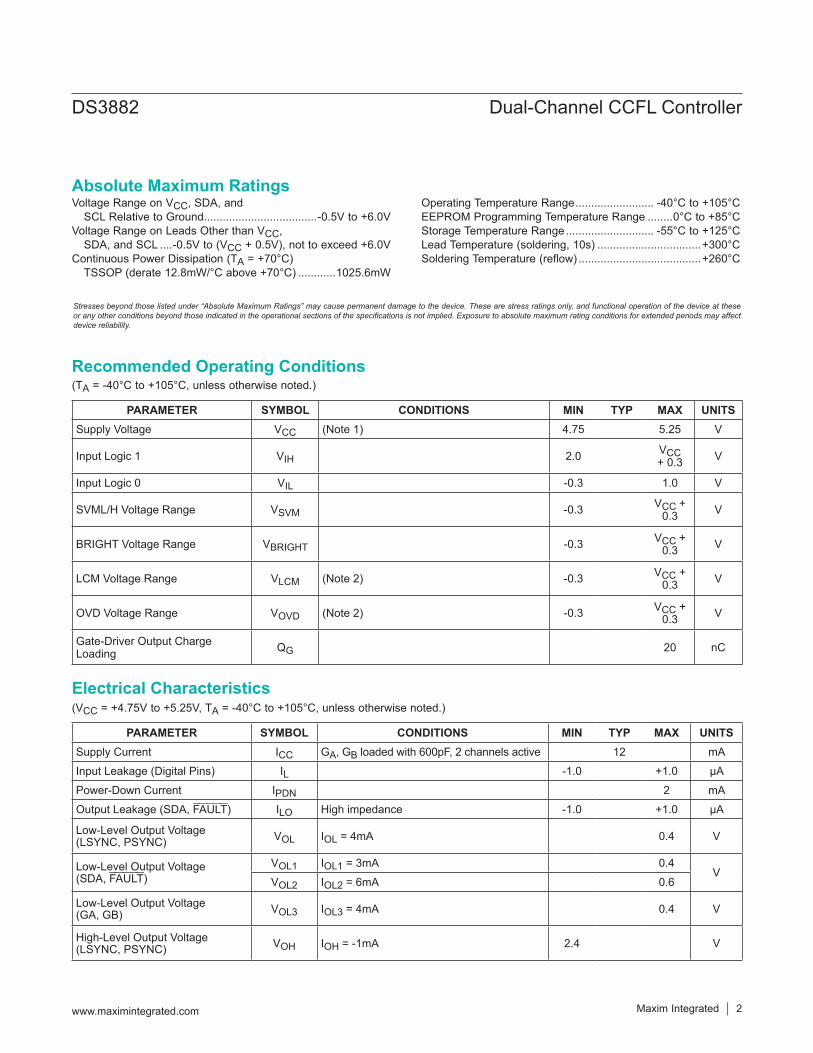
Voltage Range on VCC, SDA, and SCL Relative to Ground ....................................-0.5V to +6.0V
Voltage Range on Leads Other than VCC, SDA, and SCL ....-0.5V to (VCC + 0.5V), not to exceed +6.0V
Continuous Power Dissipation (TA = +70°C) TSSOP (derate 12.8mW/°C above +70°C) ............1025.6mW
Operating Temperature Range ......................... -40°C to +105°CEEPROM Programming Temperature Range ........0°C to +85°CStorage Temperature Range ............................ -55°C to +125°CLead Temperature (soldering, 10s) .................................+300°CSoldering Temperature (reflow) .......................................+260°C
(VCC = +4.75V to +5.25V, TA = -40°C to +105°C, unless otherwise noted.)
(TA = -40°C to +105°C, unless otherwise noted.)
PARAMETER SYMBOL CONDITIONS MIN TYP MAX UNITSSupply Current ICC GA, GB loaded with 600pF, 2 channels active 12 mA
Input Leakage (Digital Pins) IL -1.0 +1.0 µA
Power-Down Current IPDN 2 mA
Output Leakage (SDA, FAULT) ILO High impedance -1.0 +1.0 µA
Low-Level Output Voltage (LSYNC, PSYNC) VOL IOL = 4mA 0.4 V
Low-Level Output Voltage (SDA, FAULT)
VOL1 IOL1 = 3mA 0.4V
VOL2 IOL2 = 6mA 0.6
Low-Level Output Voltage (GA, GB) VOL3 IOL3 = 4mA 0.4 V
High-Level Output Voltage (LSYNC, PSYNC) VOH IOH = -1mA 2.4 V
PARAMETER SYMBOL CONDITIONS MIN TYP MAX UNITSSupply Voltage VCC (Note 1) 4.75 5.25 V
Input Logic 1 VIH 2.0 VCC + 0.3 V
Input Logic 0 VIL -0.3 1.0 V
SVML/H Voltage Range VSVM -0.3 VCC + 0.3 V
BRIGHT Voltage Range VBRIGHT -0.3 VCC + 0.3 V
LCM Voltage Range VLCM (Note 2) -0.3 VCC + 0.3 V
OVD Voltage Range VOVD (Note 2) -0.3 VCC + 0.3 V
Gate-Driver Output Charge Loading QG 20 nC
www.maximintegrated.com Maxim Integrated │ 2
DS3882 Dual-Channel CCFL Controller
Electrical Characteristics
Recommended Operating Conditions
Stresses beyond those listed under “Absolute Maximum Ratings” may cause permanent damage to the device. These are stress ratings only, and functional operation of the device at these or any other conditions beyond those indicated in the operational sections of the specifications is not implied. Exposure to absolute maximum rating conditions for extended periods may affect device reliability.
Absolute Maximum Ratings

(VCC = +4.75V to +5.25V, TA = -40°C to +105°C, unless otherwise noted.)
PARAMETER SYMBOL CONDITIONS MIN TYP MAX UNITS
High-Level Output Voltage (GA, GB) VOH1 IOH1 = -1mA VCC -
0.4 V
UVLO Threshold: VCC Rising VUVLOR 4.3 V
UVLO Threshold: VCC Falling VUVLOF 3.7 V
UVLO Hysteresis VUVLOH 200 mV
SVML/H Threshold: Rising VSVMR 2.03 2.08 2.15 V
SVML/H Threshoxc ld: Falling VSVMF 1.95 2.02 2.07 V
LCM and OVD DC Bias Voltage VDCB 1.1 V
LCM and OVD Input Resistance RDCB 50 kW
Lamp Off Threshold VLOT (Note 3) 0.22 0.25 0.28 V
Lamp Over Current VLOC (Note 3) 2.2 2.5 2.8 V
Lamp Regulation Threshold VLRT (Notes 3, 4) 0.9 1.0 1.1 V
OVD Threshold VOVDT (Note 3) 0.9 1.0 1.1 V
Lamp Frequency Source Frequency Range fLFS:OSC 40 100 kHz
Lamp Frequency Source Frequency Tolerance fLFS:TOL LOSC resistor ±2% over temperature -5 +5 %
Lamp Frequency Receiver Frequency Range fLFR:OSC 40 100 kHz
Lamp Frequency Receiver Duty Cycle fLFR:DUTY 40 60 %
DPWM Source (Resistor) Frequency Range fDSR:OSC 22.5 440.0 Hz
DPWM Source (Resistor) Frequency Tolerance fDSR:TOL POSC resistor ±2% over temperature -5 +5 %
DPWM Source (Ext. Clk) Frequency Range fDSE:OSC 22.5 440.0 Hz
DPWM Source (Ext. Clk) Duty Cycle fDFE:DUTY 40 60 %
DPWM Receiver Min Pulse Width tDR:MIN (Note 5) 25 µs
BRIGHT Voltage: Minimum Brightness VBMIN 0.5 V
BRIGHT Voltage: Maximum Brightness VBMAX 2.0 V
Gate Driver Output Rise/Fall Time tR / tF CL = 600pF 100 ns
GAn and GBn Duty Cycle (Note 6) 44 %
www.maximintegrated.com Maxim Integrated │ 3
DS3882 Dual-Channel CCFL Controller
Electrical Characteristics (continued)

Note 1: All voltages are referenced to ground unless otherwise noted. Currents into the IC are positive, out of the IC negative.Note 2: During fault conditions, the AC-coupled feedback values are allowed to be below the absolute max rating of the LCM or
OVD pin for up to 1 second.Note 3: Voltage with respect to VDCB.Note 4: Lamp overdrive and analog dimming (based on reduction of lamp current) are disabled.Note 5: This is the minimum pulse width guaranteed to generate an output burst, which generates the DS3882’s minimum burst
duty cycle. This duty cycle may be greater than the duty cycle of the PSYNC input. Once the duty cycle of the PSYNC input is greater than the DS3882’s minimum duty cycle, the output’s duty cycle tracks the PSYNC’s duty cycle. Leaving PSYNC low (0% duty cycle) disables the GAn and GBn outputs in DPWM receiver mode.
Note 6: This is the maximum lamp frequency duty cycle that is generated at any of the GAn or GBn outputs with spread-spectrum modulation disabled.
Note 7: I2C interface timing shown is for fast-mode (400kHz) operation. This device is also backward compatible with I2C stan-dard-mode timing.
Note 8: After this period, the first clock pulse can be generated.Note 9: CB—total capacitance allowed on one bus line in picofarads.Note 10: EEPROM write time applies to all the EEPROM memory. EEPROM write begins after a STOP condition occurs.Note 11: Guaranteed by design.
(VCC = +4.75V to +5.25V, unless otherwise noted.)
(VCC = +4.75V to +5.25V, TA = -40°C to +105°C, timing referenced to VIL(MAX) and VIH(MIN), unless otherwise noted.) (See Figure 9.)
PARAMETER SYMBOL CONDITIONS MIN TYP MAX UNITSEEPROM Write Cycles +85°C (Note 11) 30,000
PARAMETER SYMBOL CONDITIONS MIN TYP MAX UNITSSCL Clock Frequency fSCL (Note 7) 0 400 kHz
Bus Free Time Between STOP and START Conditions tBUF 1.3 µs
Hold Time (Repeated) START Condition tHD:STA (Note 8) 0.6 µs
Low Period of SCL tLOW 1.3 µs
High Period of SCL tHIGH 0.6 µs
Data Hold Time tHD:DAT 0 0.9 µs
Data Setup Time tSU:DAT 100 ns
Start Setup Time tSU:STA 0.6 µs
SDA and SCL Rise Time tR (Note 9) 20+ 0.1CB 300 ns
SDA and SCL Fall Time tF (Note 9) 20+ 0.1CB 300 ns
Stop Setup Time tSU:STO 0.6 µs
SDA and SCL Capacitive Loading CB (Note 9) 400 pF
EEPROM Write Time tW (Note 10) 20 30 ms
www.maximintegrated.com Maxim Integrated │ 4
DS3882 Dual-Channel CCFL Controller
Nonvolatile Memory Characteristics
I2C AC Electrical Characteristics

(VCC = 5.0V, TA = +25°C, unless otherwise noted.)
BURST DIMMING AT 150Hz AND 50%
DS38
82 to
c09
1ms5.0V GA
1ms5.0V GB
1ms2.00V LCM
1ms2.00V OVD
BURST DIMMING AT 150Hz AND 10%
DS38
82 to
c08
1ms5.0V GA
1ms5.0V GB
1ms2.00V LCM
1ms2.00V OVD
TYPICAL STARTUP WITH SVM
DS3
882
toc0
7
2ms5.0V SVML
2ms5.0V GB
2ms2.00V LCM
2ms2.00V OVD
TYPICAL OPERATION AT 16V
DS38
82 to
c06
10s5.0V GA
10s5.0V GB
10s2.00V LCM
10s2.00V OVD
TYPICAL OPERATION AT 13V DS
3882
toc0
5
10s5.0V GA
10s5.0V GB
10s2.00V LCM
10s2.00V OVD
TYPICAL OPERATION AT 11V
DS38
82 to
c04
10s5.0V GA
10s5.0V GB
10s2.00V LCM
10s2.00V OVD
INTERNAL FREQUENCY CHANGEvs. TEMPERATURE
DS38
82 to
c03
TEMPERATURE (°C)
FREQ
UENC
Y CH
ANGE
(%)
32.5
-0.8
-0.6
-0.4
-0.2
0
0.2
0.4
0.6
0.8
1.0
-1.0-40.0 105
DPWM FREQUENCY
LAMP FREQUENCY
ACTIVE SUPPLY CURRENTvs. TEMPERATURE
DS38
82 to
c02
TEMPERATURE (°C)
SUPP
LY C
URRE
NT (m
A)
32.5
5.7
5.9
6.1
6.3
6.5
6.7
6.9
7.1
7.3
7.5
5.5-40.0 105
VCC = 4.75V VCC = 5.0VVCC = 5.25V
DPWM = 100%
fLF:OSC = 64kHz
GATE QC = 3.5nC
ACTIVE SUPPLY CURRENTvs. SUPPLY VOLTAGE
DS38
82 to
c01
SUPPLY VOLTAGE (V)
SUPP
LY C
URRE
NT (m
A)
5.205.154.80 4.85 4.90 5.00 5.054.95 5.10
4.5
5.0
5.5
6.0
6.5
7.0
7.5
8.0
4.04.75 5.25
DPWM = 10%DPWM = 50%
DPWM = 100%
SVML< 2V
fLF:OSC = 64kHzGATE QC = 3.5nC
Maxim Integrated │ 5www.maximintegrated.com
DS3882 Dual-Channel CCFL Controller
Typical Operating Characteristics

(VCC = 5.0V, TA = +25°C, unless otherwise noted.)
LAMP OUT (LAMP OPENED),AUTORETRY DISABLED
DS38
82 to
c14
0.1s5.0V GA
0.1s5.0V GB
0.1s2.00V LCM
0.1s2.00V OVD
LAMP OPENED
STAGGERED BURST DIMMING START
DS38
82 to
c13
0.2ms2.00V GA1
0.2ms2.00V GA2
LAMP STRIKE WITH OPEN LAMP,AUTO RETRY DISABLED
DS38
82 to
c12
0.5s5.0V GA
0.5s5.0V GB
0.5s2.00V LCM
0.5s2.00 OVD
LAMP STRIKE—EXPANDED VIEW
DS38
82 to
c11
1ms5.0V GA
1ms5.0V GB
1ms2.00V LCM
1ms2.00V OVD
SOFT-START AT VINV = 16VDS
3882
toc1
0
50s5.0V GA
50s5.0V GB
50s2.00V LCM
50s2.00V OVD
Maxim Integrated │ 6www.maximintegrated.com
DS3882 Dual-Channel CCFL Controller
Typical Operating Characteristics (continued)

NAMEPINS BY
CHANNEL (n) FUNCTIONCH 1 CH 2
GAn 15 25 MOSFET A Gate Drive. Connect directly to logic-level mode n-channel MOSFET. Leave open if channel is unused.
GBn 16 26 MOSFET B Gate Drive. Connect directly to logic-level mode n-channel MOSFET. Leave open if channel is unused.
LCMn 17 27 Lamp Current Monitor Input. Lamp current is monitored by a resistor placed in series with the low-voltage side of the lamp. Leave open if channel is unused.
OVDn 18 28 Overvoltage Detection. Lamp voltage is monitored by a capacitor divider placed on the high-voltage side of the transformer. Leave open if channel is unused.
NAME PIN FUNCTIONFAULT 1 Active-Low Fault Output. This open-drain pin requires external pullup resistor to realize high logic levels.
A0 2 Address Select Input. Determines I2C slave address.
SDA 3 Serial-Data Input/Output. I2C bidirectional data pin, which requires a pullup resistor to realize high logic levels.
SCL 4 Serial Clock Input. I2C clock input.
LSYNC 5Lamp Frequency Input/Output. This pin is the input for an externally sourced lamp frequency when the DS3882 is configured as a lamp frequency receiver. If the DS3882 is configured as a lamp frequency source (i.e., the lamp frequency is generated internally), the frequency is output on this pin for use by other lamp frequency receiver DS3882s.
LOSC 6 Lamp Oscillator Resistor Adjust. A resistor to ground on this pin sets the frequency of the internal lamp oscillator.
BRIGHT 7 Analog Brightness Control Input. Used to control the DPWM dimming feature. Ground if unused.
PSYNC 8DPWM Input/Output. This pin is the input for an externally generated DPWM signal when the DS3882 is configured as a DPWM receiver. If the DS3882 is configured as a DPWM source (i.e., the DPWM signal is generated internally), the DPWM signal is output on this pin for use by other DPWM receiver DS3882s.
www.maximintegrated.com Maxim Integrated │ 7
DS3882 Dual-Channel CCFL Controller
Pin Description
NAME PIN FUNCTION
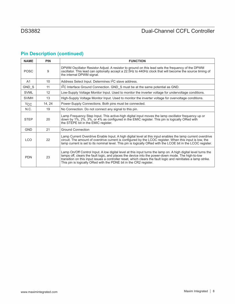
POSC 9DPWM Oscillator Resistor Adjust. A resistor to ground on this lead sets the frequency of the DPWM oscillator. This lead can optionally accept a 22.5Hz to 440Hz clock that will become the source timing of the internal DPWM signal.
A1 10 Address Select Input. Determines I2C slave address.
GND_S 11 I2C Interface Ground Connection. GND_S must be at the same potential as GND.
SVML 12 Low-Supply Voltage Monitor Input. Used to monitor the inverter voltage for undervoltage conditions.
SVMH 13 High-Supply Voltage Monitor Input. Used to monitor the inverter voltage for overvoltage conditions.
VCC 14, 24 Power-Supply Connections. Both pins must be connected.
N.C. 19 No Connection. Do not connect any signal to this pin.
STEP 20Lamp Frequency Step Input. This active-high digital input moves the lamp oscillator frequency up or down by 1%, 2%, 3%, or 4% as configured in the EMIC register. This pin is logically ORed with the STEPE bit in the EMIC register.
GND 21 Ground Connection
LCO 22Lamp Current Overdrive Enable Input. A high digital level at this input enables the lamp current overdrive circuit. The amount of overdrive current is configured by the LCOC register. When this input is low, the lamp current is set to its nominal level. This pin is logically ORed with the LCOE bit in the LCOC register.
PDN 23Lamp On/Off Control Input. A low digital level at this input turns the lamp on. A high digital level turns the lamps off, clears the fault logic, and places the device into the power-down mode. The high-to-low transition on this input issues a controller reset, which clears the fault logic and reinitiates a lamp strike. This pin is logically ORed with the PDNE bit in the CR2 register.
www.maximintegrated.com Maxim Integrated │ 8
DS3882 Dual-Channel CCFL Controller
Pin Description (continued)
Figure 1. Functional Diagram
GAn MOSFETGATEDRIVERS
GBn
OVDnOVERVOLTAGEDETECTION
LAMP FREQUENCYINPUT/OUTPUT [20.48MHz ~ 51.20MHz]
I2C DEVICECONFIGURATION AND
CONTROL PORT
22.5Hz TO 440Hz
EXTERNAL RESISTORLAMP FREQUENCY SET
GND
TWOINDEPENDENT
CCFLCONTROLLERS
EXTERNAL RESISTORDPWM FREQUENCY
SET/DPWM CLOCK INPUT
DPWM SIGNALINPUT/OUTPUT
ANALOG BRIGHTNESSCONTROL
SVMHSUPPLY VOLTAGEMONITOR—HIGH
[40kHz ~ 100kHz]
SystemEnable /
POR
EEPROM
8 BYTE USER MEMORY
CONTROL REGISTERS
FAULTCHANNEL FAULT
CHANNEL ENABLE
SDA
SCL
LSYNC
LOSC
PSYNC
BRIGHT
DPWMSIGNAL
2.0VSTATUS REGISTERS
PDN
LCO
2.0VSVMLSUPPLY VOLTAGEMONITOR—LOW
STEPSTEP LAMP FREQUENCYUP OR DOWN
40kHz TO 100kHzOSCILLATOR (5%)
LCMnLAMP CURRENTMONITOR
VCC[4.75V TO 5.25V]
x512PLL
I2CINTERFACE
SYSTEMENABLE/
POR
FAULTHANDLING
22.5Hz TO440Hz
OSCILLATOR(5%)
POSC
A0/A1GND_S
DPSS BITAT CR1.3
LFSS BITAT CR1.2
UVLO
VREF
MUXPOSCS BITAT CR1.1
MUXRGSO BITAT CR1.4
MUXDPSS BITAT CR1.3
RAMPGENERATOR
DS3882
www.maximintegrated.com Maxim Integrated │ 9
DS3882 Dual-Channel CCFL Controller
Functional Diagrams

Detailed DescriptionThe DS3882 uses a push-pull drive scheme to convert a DC voltage (8V to 16V) to the high-voltage (300VRMS to 1000VRMS) AC waveform that is required to power the CCFLs. The push-pull drive scheme uses a minimal number of external components, which reduces assembly cost and makes the printed circuit board design easy to implement. The push-pull drive scheme also provides an efficient DC-to-AC conversion and produces near-sinusoi-dal waveforms.Each DS3882 channel drives two logic-level n-channel MOSFETs that are connected between the ends of a step-up transformer and ground (see the Typical Operating Circuit). The transformer has a center tap on the prima-ry side that is connected to a DC voltage supply. The DS3882 alternately turns on the two MOSFETs to create the high-voltage AC waveform on the secondary side. By varying the duration of the MOSFET turn-on times, the CCFL current is able to be accurately controlled.A resistor in series with the CCFL’s ground connection enables current monitoring. The voltage across this resistor is fed to the lamp current monitor (LCM) input and compared to an internal reference voltage to deter-
mine the duty cycle for the MOSFET gates. Each CCFL receives independent current monitoring and control, which maximizes the lamp’s brightness and lifetime.Block diagrams of the DS3882 are shown in Figures 1 and 2. More operating details of the DS3882 are dis-cussed on the following pages of this data sheet.
Memory Registers and I2C-Compatible Serial InterfaceThe DS3882 uses an I2C-compatible serial interface for communication with the on-board EEPROM and SRAM configuration/status registers as well as user memory. The configuration registers, which are a mixture of shadowed EEPROM and SRAM, allow the user to customize many DS3882 parameters such as the soft-start ramp rate, the lamp and dimming frequency sources, brightness of the lamps, fault-monitoring options, channel enabling/dis-abling, EMI control, and lamp current overdrive control. The 8 bytes of NV user memory can be used to store manufacturing data such as date codes, serial numbers, or product identification numbers. The device is shipped from the factory with the configuration registers pro-grammed to a set of default configuration parameters. To inquire about custom programming, contact the factory.
Figure 2. Per Channel Logic Diagram
GATEDRIVERS
MOSFETGATE
DRIVERS
GAn
GBn
DIGITALCCFL
CONTROLLER
CHANNEL FAULT
512 X LAMP FREQUENCY[20.48MHz ~ 51.20MHz]
LAMP FREQUENCY[40kHz ~ 80kHz]
DIMMING PWM SIGNAL
CHANNEL ENABLE
VLRT (1.0V NOMINAL)
LCMnLAMP CURRENTMONITOR
300mV
2.5VLAMP OVERCURRENT
LAMP STRIKE AND REGULATION
LOCE BIT IN CR1.0
LAMP OUT
1.0V
OVDnOVERVOLTAGE DETECTOR
LAMP MAXIMUM VOLTAGE REGULATION
64 LAMP CYCLEINTEGRATOR
OVERVOLTAGE
www.maximintegrated.com Maxim Integrated │ 10
DS3882 Dual-Channel CCFL Controller
Functional Diagrams (continued)

Shadowed EEPROMThe DS3882 incorporates SRAM-shadowed EEPROM memory locations for all memory that needs to be retained during power cycling. At power-up, SEEB (bit 7 of the BLC register) is low which causes the shadowed locations to act as ordinary EEPROM. Setting SEEB high disables the EEPROM write function and causes the shadowed locations to function as ordinary SRAM cells. This allows an infinite number of write cycles with-out causing EEPROM damage and also eliminates the EEPROM write time, tW from the write cycle. Because memory changes made when SEEB is set high are not written to EEPROM, these changes are not retained through power cycles, and the power-up EEPROM val-ues are the last values written with SEEB low.
Channel PhasingThe lamp-frequency MOSFET gate turn-on times are out of phase between the two channels during the burst period. This reduces the inrush current that would result from all lamps switching simultaneously, and hence eases the design requirements for the DC supply. It is important to note that it is the lamp-frequency signals that are phased, not the DPWM (burst) signals.
Lamp Dimming ControlThe DS3882 provides two independent methods of lamp dimming that can be combined to achieve a dimming ratio of 300:1 or greater. The first method is “burst” dimming, which uses a digital pulse-width-modulated (DPWM) signal (22.5Hz to 440Hz) to control the lamp brightness. The second is “analog” dimming, which is accomplished by adjusting the lamp current. Burst dimming provides 128 linearly spaced brightness steps. Analog dimming provides smaller substeps that allow incremental bright-ness changes between burst dimming steps. This ability is especially useful for low-brightness dimming changes, where using burst dimming alone would cause visible brightness step changes. Analog dimming also allows the brightness to be reduced below the minimum burst dimming level, which provides for the maximum dimming range.Burst dimming can be controlled using a user-supplied analog voltage on the BRIGHT pin or through the I2C interface. Analog dimming can only be controlled through the I2C interface. Therefore, for applications that require the complete dimming range and resolution capability of the DS3882, I2C dimming control must be used.
Burst DimmingBurst dimming increases/decreases the brightness by adjusting (i.e., modulating) the duty cycle of the DPWM signal. During the high period of the DPWM cycle, the lamps are driven at the selected lamp frequency
(40kHz to 100kHz) as shown in Figure 6. This part of the cycle is called the “burst” period because of the lamp frequency burst that occurs during this time. During the low period of the DPWM cycle, the controller disables the MOSFET gate drivers so the lamps are not driven. This causes the current to stop flowing in the lamps, but the time is short enough to keep the lamps from de-ionizing.The DS3882 can generate its own DPWM signal internal-ly (set DPSS = 0 in CR1), which can then be sourced to other DS3882s if required, or the DPWM signal can be supplied from an external source (set DPSS = 1 in CR1). To generate the DPWM signal internally, the DS3882 requires a clock (referred to as the dimming clock) to set the DPWM frequency. The user can supply the dimming clock by setting POSCS = 1 in CR1 and applying an external 22.5Hz to 440Hz signal at the POSC pin, or the dimming clock can be generated by the DS3882’s inter-nal oscillator (set POSCS = 0 in CR1), in which case the frequency is set by an external resistor at the POSC pin. These two dimming clock options are shown in Figure 3. Regardless of whether the dimming clock is generat-ed internally or sourced externally, the POSCR0 and POSCR1 bits in CR2 must be set to match the desired dimming clock frequency.The internally generated DPWM signal can be provided at the PSYNC I/O pin (set RGSO = 0 in CR1) for sourc-ing to other DS3882s, if any, in the circuit. This allows all DS3882s in the system to be synchronized to the same DPWM signal. A DS3882 that is generating the DPWM signal for other DS3882s in the system is referred to as the DPWM source. When bringing in an externally gen-erated DPWM signal, either from another DS3882 acting as a DPWM source or from some other user-provided source, it is input into the PSYNC I/O pin of the DS3882, and the receiving DS3882 is referred to a DPWM receiver. In this mode, the BRIGHT and POSC inputs are disabled and should be grounded (see Figure 5).When the DPWM signal is generated internally, its duty cycle (and, thus, the lamp brightness) is controlled either by a user-supplied analog voltage at the BRIGHT input or through the I2C interface by varying the 7-bit PWM code in the BPWM register. When using the BRIGHT pin to control burst dimming, a voltage of less than 0.5V causes the DS3882 to operate with the minimum burst duty cycle, pro-viding the lowest brightness setting, while any voltage great-er than 2.0V causes a 100% burst duty cycle (i.e., lamps always being driven), which provides the maximum bright-ness. For voltages between 0.5V and 2V, the duty cycle varies linearly between the minimum and 100%. Writing a
www.maximintegrated.com Maxim Integrated │ 11
DS3882 Dual-Channel CCFL Controller
non-zero PWM code to the BPWM register disables the BRIGHT pin and enables I2C burst dimming control. Setting the 7-bit PWM code to 0000001b causes the DS3882 to operate with the minimum burst duty cycle, while a setting of 1111111b causes a 100% burst duty cycle. For settings between these two codes, the duty cycle varies linearly between the minimum and 100%.
Analog DimmingAnalog dimming changes the brightness by increasing or decreasing the lamp current. The DS3882 accom-plishes this by making small shifts to the lamp regula-tion voltage, VLRT (see Figure 2). Analog dimming is only possible by software communication with the lower five bits (LC4–LC0) in the BLC register. This function is not pin controllable. The default power-on state of the LC bits is 00000b, which corresponds to 100% of the nominal current level. Therefore on power-up, ana-log dimming does not interfere with burst dimming functionality if it is not desired. Setting the LC bits to 11111b reduces the lamp current to 35% of its nominal level. For LC values between 11111b and 00000b, the lam current varies linearly between 35% and 100% of nominal.
Lamp Frequency ConfigurationThe DS3882 can generate its own lamp frequency clock internally (set LFSS = 0 in CR1), which can then be sourced to other DS3882s if required, or the lamp clock can be supplied from an external source (set LFSS = 1 in CR1). When the lamp clock is internally generated, the frequency (40kHz to 100kHz) is set by
an external resistor at the LOSC. In this case, the DS3882 can act as a lamp frequency source because the lamp clock is output at the LSYNC I/O pin for synchronizing any other DS3882s configured as lamp frequency receivers. While DS3882 is sourcing lamp frequency to other DS3882’s and spread-spectrum modulation or frequency step features are enabled, the LSYNC output is not affected by either EMI suppression features. The DS3882 acts as a lamp frequency receiv-er when the lamp clock is supplied externally. In this case, a 40kHz to 100kHz clock must be supplied at the LSYNC I/O. The external clock can originate from the LSYNC I/O of a DS3882 configured as a lamp frequency source or from some other source.
Figure 4. DPWM Receiver Configuration
Figure 3. DPWM Source Configuration Options
BRIGHT
PSYNC
POSC22.5Hz TO 440Hz
DPWMSIGNAL
DPWM RECEIVER
BRIGHT
PSYNC
POSC
2.0V
0.5V
22.5Hz TO 440Hz
EXTERNAL RESISTORSETS DPWM RATE
DPWMSIGNAL
ANALOG DIMMINGCONTROL VOLTAGE
RESISTOR-SET DIMMING CLOCK
BRIGHT
PSYNC
POSC
2.0V
0.5V
22.5Hz TO 440Hz
22.5Hz to 440Hz
DPWMSIGNAL
EXTERNALDPWM CLOCK
ANALOG DIMMINGCONTROL VOLTAGE
EXTERNAL DIMMING CLOCK
www.maximintegrated.com Maxim Integrated │ 12
DS3882 Dual-Channel CCFL Controller
Figure 5. Frequency Configuration Options for Designs Using Multiple DS3882s
2.0VBRIGHT
LAMP FREQUENCY SOURCEDPWM SOURCE
PSYNCLSYNCPOSCLOSC
0.5V
RESISTOR-SETDIMMING
FREQUENCY
RESISTOR-SETLAMP FREQUENCY
DS3882
BRIGHT
LAMP FREQUENCY RECEIVERDPWM RECEIVER
PSYNC
LSYNCPOSCLOSC
DS3882
2.0VBRIGHT
LAMP FREQUENCY SOURCEDPWM SOURCE
PSYNCLSYNCPOSCLOSC
0.5V
ANALOGBRIGHTNESS
ANALOGBRIGHTNESS
RESISTOR-SETLAMP FREQUENCY
DIMMING CLOCK(22.5Hz TO 440Hz)
DPWM SIGNAL(22.5Hz TO 440Hz)
DS3882
BRIGHT
LAMP FREQUENCY RECEIVERDPWM RECEIVER
PSYNC
LSYNCPOSCLOSC
DS3882
BRIGHT
LAMP FREQUENCY SOURCEDPWM RECEIVER
PSYNCLSYNCPOSCLOSCRESISTOR-SET
LAMP FREQUENCY
DS3882
BRIGHT
LAMP FREQUENCY RECEIVERDPWM RECEIVER
PSYNC
LSYNCPOSCLOSC
DS3882
2.0VBRIGHT
LAMP FREQUENCY RECEIVERDPWM SOURCE
PSYNCLSYNCPOSCLOSCN.C.
N.C.N.C.
N.C.
N.C.
N.C.
N.C.N.C.
N.C.N.C.
N.C.N.C.
N.C.N.C.
N.C.
N.C.N.C.
0.5V
RESISTOR-SETDIMMING FREQUENCY
DS3882
BRIGHT
LAMP FREQUENCY RECEIVERDPWM RECEIVER
PSYNC
LSYNCPOSCLOSC
DS3882
2.0VBRIGHT
LAMP FREQUENCY RECEIVERDPWM SOURCE
PSYNCLSYNCPOSCLOSC
0.5V
ANALOGBRIGHTNESS
ANALOGBRIGHTNESS
LAMP CLOCK(40kHz TO 100kHz)
DIMMING CLOCK(22.5Hz TO 440Hz)
LAMP CLOCK(40kHz TO 100kHz)
DPWM SIGNAL(22.5Hz TO 440Hz)
LAMP CLOCK(40kHz TO 100kHz)
DS3882
BRIGHT
LAMP FREQUENCY RECEIVERDPWM RECEIVER
PSYNC
LSYNCPOSCLOSC
DS3882
BRIGHT
LAMP FREQUENCY RECEIVERDPWM RECEIVER
PSYNCLSYNCPOSCLOSC
DS3882
BRIGHT
LAMP FREQUENCY RECEIVERDPWM RECEIVER
PSYNC
LSYNCPOSCLOSC
DS3882
www.maximintegrated.com Maxim Integrated │ 13
DS3882 Dual-Channel CCFL Controller
Configuring Systems with Multiple DS3882sThe source and receiver options for the lamp frequency clock and DPWM signal allow multiple DS3882s to be synchronized in systems requiring more than two lamps. The lamp and dimming clocks can either be generated on board the DS3882 using external resistors to set the frequency, or they can be sourced by the host system to synchronize the DS3882 to other system resources. Figure 5 shows various multiple DS3882 configurations that allow both lamp and/or DPWM synchronization for all DS3882s in the system.
DPWM Soft-StartAt the beginning of each lamp burst, the DS3882 pro-vides a soft-start that slowly increases the MOSFET
gate-driver duty cycle (see Figure 6). This minimizes the possibility of audible transformer noise that could result from current surges in the transformer primary. The soft-start length is fixed at 16 lamp cycles, but the soft-start ramp profile is programmable through the four soft-start profile registers (SSP1/2/3/4) and can be adjusted to match the application. There are seven different driver duty cycles to select from to customize the soft-start ramp (see Tables 5a and 5b). The available duty cycles range from 0% to 19% in ~3% increments. In addition, the MOSFET duty cycle from the last lamp cycle of the previous burst can be used as part of the soft-start ramp by using the most recent value duty cycle code. Each programmed MOSFET gate duty cycle repeats twice to make up the 16 soft-start lamp cycles.
Figure 6. Digital PWM Dimming and Soft-Start
1615141312111098765432
SSP1. 0-3
LAMP CURRENT
SOFT-START PROFILE REGISTER
SOFT-START
SOFT-START (EXPANDED)
22.5Hz TO 440Hz
DPWM SIGNAL
LAMP CURRENT
LAMP CYCLE GAn/GBn
MOSFET GATE DRIVERS
PROGRAMMABLE SOFT-START PROFILE WITH INCREASING MOSFET PULSE WIDTHS OVERA 16 LAMP CYCLE PERIOD RESULTS IN A LINEAR RAMP IN LAMP CURRENT.
SSP1. 4-7 SSP2. 0-3 SSP2. 4-7 SSP3. 0-3 SSP3. 4-7 SSP4. 0-3 SSP4. 4-7
1
www.maximintegrated.com Maxim Integrated │ 14
DS3882 Dual-Channel CCFL Controller
Setting the Lamp and Dimming Clock (DPWM) Frequencies Using External ResistorsBoth the lamp and dimming clock frequencies can be set using external resistors. The resistance required for either frequency can be determined using the following formula:
OSCOSC
KR f
=
where K = 1600kW ● kHz for lamp frequency calculations. When calculating the resistor value for the dimming clock frequency, K will be one of four values as determined by the desired frequency and the POSCR0 and POSCR1 bit settings as shown in the Control Register 2 (CR2) Table 7 in the Detailed Register Descriptions section.Example: Selecting the resistor values to configure a DS3882 to have a 50kHz lamp frequency and a 160Hz dimming clock frequency: For this configuration, POSCR0 and POSCR1 must be programmed to 1 and 0, respec-tively, to select 90Hz to 220Hz as the dimming clock frequency range. This sets K for the dimming clock resis-tor (RPOSC) calculation to 4kW ● kHz. For the lamp fre-quency resistor (RLOSC) calculation, K = 1600kW ● kHz, which sets the lamp frequency K value regardless of the frequency. The formula above can now be used to calcu-late the resistor values for RLOSC and RPOSC as follows:
LOSC
POSC
1600k kHzR 32.0k50kHz
4k kHzR 25.0k0.160kHz
W •= = W
W •= = W
Supply MonitoringThe DS3882 has supply voltage monitors (SVMs) for both the inverter’s transformer DC supply (VINV) and its own VCC supply to ensure that both voltage levels are adequate for proper operation. The transformer supply is monitored for overvoltage conditions at the SVMH pin and undervoltage conditions at the SVML pin. External resistor-dividers at each SVM input feed into two comparators (see Figure 7), both having 2V thresholds. Using the equation below to determine the resistor values, the SVMH and SVML trip points (VTRIP) can be customized to shut off the inverter when the transformer’s supply voltage rises above or drops below specified values. Operating with the transformer’s sup-ply at too low of a level can prevent the inverter from
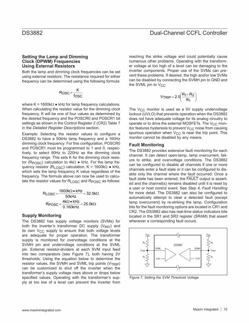
reaching the strike voltage and could potentially cause numerous other problems. Operating with the transform-er voltage at too high of a level can be damaging to the inverter components. Proper use of the SVMs can pre-vent these problems. If desired, the high and/or low SVMs can be disabled by connecting the SVMH pin to GND and the SVML pin to VCC
1 2TRIP
1
R RV 2.0R+ =
The VCC monitor is used as a 5V supply undervoltage lockout (UVLO) that prevents operation when the DS3882 does not have adequate voltage for its analog circuitry to operate or to drive the external MOSFETs. The VCC mon-itor features hysteresis to prevent VCC noise from causing spurious operation when VCC is near the trip point. This monitor cannot be disabled by any means.
Fault MonitoringThe DS3882 provides extensive fault monitoring for each channel. It can detect open-lamp, lamp overcurrent, fail-ure to strike, and overvoltage conditions. The DS3882 can be configured to disable all channels if one or more channels enter a fault state or it can be configured to dis-able only the channel where the fault occurred. Once a fault state has been entered, the FAULT output is assert-ed and the channel(s) remains disabled until it is reset by a user or host control event. See Step 4, Fault Handling for more detail. The DS3882 can also be configured to automatically attempt to clear a detected fault (except lamp overcurrent) by re-striking the lamp. Configuration bits for the fault monitoring options are located in CR1 and CR2. The DS3882 also has real-time status indicators bits located in the SR1 and SR2 register (SRAM) that assert whenever a corresponding fault occurs.
Figure 7. Setting the SVM Threshold Voltage
SVML
R2
R1 2.0V
VINV
SVMH
R2
VTRIPVTRIP
R12.0V
VINV
DS3882
www.maximintegrated.com Maxim Integrated │ 15
DS3882 Dual-Channel CCFL Controller

Figure 8 shows a flowchart of how the DS3882 controls and monitors each lamp. The steps are as follows:1) Supply Check—The lamps do not turn on unless the
DS3882 supply voltage is above 4.3V and the voltage at the supply voltage monitors, SVML and SVMH, are respectively above 2.0V and below 2.0V.
2) Strike Lamp—When both the DS3882 and the DC inverter supplies are at acceptable levels, the DS3882 attempts to strike each enabled lamp. The DS3882 slowly ramps up the MOSFET gate duty cycle until the lamp strikes. The controller detects that the lamp has struck by detecting current flow in the lamp, detect-ed by the LCMn pin. If during the strike ramp, the maximum allowable voltage is reached on the OVDn pin, the controller stops increasing the MOSFET gate duty cycle to keep from overstressing the system. The DS3882 goes into a fault handling state (step 4) if the lamp has not struck after the timeout period as defined by the LST0 and LST1 control bits in the SSP1 register. If an overvoltage event is detected during the strike attempt, the DS3882 disables the MOSFET gate drivers and go into the fault handling state.
3) Run Lamp—Once the lamp is struck, the DS3882 adjusts the MOSFET gate duty cycle to optimize the lamp current. The gate duty cycle is always constrained to keep the system from exceeding the maximum allowable lamp voltage. The lamp current sampling rate is user-selectable using the LSR0 and
LSR1 bits in CR2. If lamp current ever drops below the lamp out reference point for the period as defined by the LST0 and LST1 control bits in the SSP1 register, then the lamp is considered extinguished. In this case, the MOSFET gate drivers are disabled and the device moves to the fault handling stage.
4) Fault Handling—During fault handling, the DS3882 performs an optional (user-selectable) automatic retry to attempt to clear all faults except a lamp overcurrent. The automatic retry makes 14 additional attempts to rectify the fault before declaring the channel in a fault state and permanently disabling the channel. Between each of the 14 attempts, the controller waits 1024 lamp cycles. In the case of a lamp overcurrent, the DS3882 instantaneously declares the channel to be in a fault state and permanently disables the channel. The DS3882 can be configured to disable all channels if one or more channels enter a fault state or it can be configured to disable only the channel where the fault occurred. Once a fault state is entered, the channel remains in that state until one of the following occurs:
● VCC drops below the UVLO threshold. ● The SVML or SVMH thresholds are crossed. ● The PDN pin goes high. ● The PDNE software bit is written to a logic 1. ● The channel is disabled by the CH1D or CH2D
control bit.
www.maximintegrated.com Maxim Integrated │ 16
DS3882 Dual-Channel CCFL Controller

Figure 8. Fault-Handling Flowchart
MOSFET GATE DRIVERS ENABLED
DEVICE ANDINVERTER SUPPLIESAT PROPER LEVELS?
STRIKE LAMP[RAMP AND REGULATE TO
OVD THRESHOLD]
FAULT WAIT[1024 LAMP CYCLES]
LAMP STRIKE TIMEOUT[SEE REGISTER SSP1]
RUN LAMP[REGULATE LAMP
CURRENT BOUNDED BYLAMP VOLTAGE]
LAMP OUT TIMEOUT[SEE REGISTER SSP1]
INCREMENT FAULTCOUNTER / SET
FAULT_RT STATUS BIT
FAULT COUNTER = 15?
FAULT STATE[ACTIVATE FAULT OUTPUT]
LAMP OVERCURRENT[INSTANTANEOUS IF
ENABLED BY THELOCE BIT AT CR1.0]
NOYES
AUTORETRY ENABLED?[ARD BIT AT CR1.5]
NO YES
YES
OVERVOLTAGE[64 LAMP CYCLES]
SET LOUT_LSTATUS BIT
SET OV_LSTATUS BIT
SET STO_LSTATUS BIT
SET LOC_LSTATUS BIT
CLEARFAULT_RT
STATUS BIT
IF LAMP REGULATIONTHRESHOLD IS MET
RESET FAULT COUNTERAND FAULT OUTPUT
SET FAULT_LAND FAULT_RTSTATUS BITS
www.maximintegrated.com Maxim Integrated │ 17
DS3882 Dual-Channel CCFL Controller
EMI Suppression FunctionalityThe DS3882 contains two electromagnetic interference suppression features: spread-spectrum modulation and lamp oscillator frequency stepping. The first is the ability to spread the spectrum of the lamp frequency. By setting either SS0 and/or SS1 in EMIC register, the controller can be configured to dither the lamp frequency by ±1.5%, ±3%, or ±6%. By setting a non-zero value in SS0/1, spread-spectrum modulation is enabled and oscillator frequency stepping is disabled. In spread-spectrum mod-ulation mode the dither modulation rate is also selectable by setting FS0/1/2, and has either a triangular (SSM = 0) or a pseudorandom profile (SSM = 1). Users have the flexibility to choosing the best modulation rate (through FS0/1/2) for the application.The second EMI suppression scheme is the ability to move the lamp frequency up or down by 1%, 2%, 3%, or 4%. In this scheme, the actual radiated EMI is not reduced but it is moved out of a sensitive frequency region. STEPE bit and/or STEP pin is used to enable lamp frequency stepping (SS0/1 must be 0). Once enabled, the FS0/1/2 value controls the lamp oscillator frequency shift. For example, if the lamp frequency creates EMI disturbing an audio radio station, it can be moved up or down slightly to slide the spurious interferer out of band.
Lamp Current Overdrive FunctionalityAnother feature the DS3882 offers is the ability to over-drive the lamps to allow them to heat up quickly in cold environments. After setting the LCO0/1/2 bits in the LCOC register and enabling the LCOE bit or LCO pin, the DS3882 overdrives the nominal current settings in 12.5% steps from 112.5% up to 200%. The DS3882 accom-plishes this by automatically shifting the lamp regulation threshold, VLRT, upward to allow more current to flow in the lamps (Figure 2). This multilevel adjustment makes it possible to slowly decrease the current overdrive (through I2C) after the lamps have warmed up, so the end user does not see any change in brightness when the over-drive is no longer needed. The DS3882 also features an optional timer capable of automatically turning off the cur-rent overdrive. This timer is adjustable from approximately 1.5 minutes to 21 minutes (if a 50kHz lamp frequency is used).
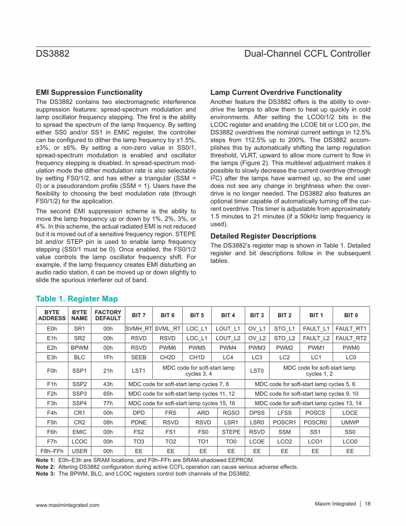
Detailed Register DescriptionsThe DS3882’s register map is shown in Table 1. Detailed register and bit descriptions follow in the subsequent tables.
Note 1: E0h–E3h are SRAM locations, and F0h–FFh are SRAM-shadowed EEPROM.Note 2: Altering DS3882 configuration during active CCFL operation can cause serious adverse effects.Note 3: The BPWM, BLC, and LCOC registers control both channels of the DS3882.
Table 1. Register MapBYTE
ADDRESSBYTE NAME
FACTORY DEFAULT BIT 7 BIT 6 BIT 5 BIT 4 BIT 3 BIT 2 BIT 1 BIT 0
E0h SR1 00h SVMH_RT SVML_RT LOC_L1 LOUT_L1 OV_L1 STO_L1 FAULT_L1 FAULT_RT1
E1h SR2 00h RSVD RSVD LOC_L1 LOUT_L2 OV_L2 STO_L2 FAULT_L2 FAULT_RT2
E2h BPWM 00h RSVD PWM6 PWM5 PWM4 PWM3 PWM2 PWM1 PWM0
E3h BLC 1Fh SEEB CH2D CH1D LC4 LC3 LC2 LC1 LC0
F0h SSP1 21h LST1 MDC code for soft-start lamp cycles 3, 4 LST0 MDC code for soft-start lamp
cycles 1, 2
F1h SSP2 43h MDC code for soft-start lamp cycles 7, 8 MDC code for soft-start lamp cycles 5, 6
F2h SSP3 65h MDC code for soft-start lamp cycles 11, 12 MDC code for soft-start lamp cycles 9, 10
F3h SSP4 77h MDC code for soft-start lamp cycles 15, 16 MDC code for soft-start lamp cycles 13, 14
F4h CR1 00h DPD FRS ARD RGSO DPSS LFSS POSCS LOCE
F5h CR2 08h PDNE RSVD RSVD LSR1 LSR0 POSCR1 POSCR0 UMWP
F6h EMIC 00h FS2 FS1 FS0 STEPE RSVD SSM SS1 SS0
F7h LCOC 00h TO3 TO2 TO1 TO0 LCOE LCO2 LCO1 LCO0
F8h–FFh USER 00h EE EE EE EE EE EE EE EE
www.maximintegrated.com Maxim Integrated │ 18
DS3882 Dual-Channel CCFL Controller

Note 1: Writing to this register has no effect on it.Note 2: See Figure 8 for more details on how the status bits are set.Note 3: SR1 is cleared when any of the following occurs:
● VCC drops below the UVLO threshold ● the SVML or SVMH thresholds are crossed ● the PDN hardware pin goes high ● the PDNE software bit is written to a logic 1 ● the channel is disabled by the CH1D control bit
Table 2. Status Register 1 (SR1) [SRAM, E0h]
BIT R/W POWER-UP DEFAULT NAME FUNCTION
0 R 0 FAULT_RTFault Condition—Real Time. A real-time bit that indicates the current operating status of channel 1. 0 = Normal condition 1 = Fault condition
1 R 0 FAULT_L Fault Condition—Latched. A latched bit that is set when the channel enters a fault condition. This bit is cleared when read, regardless of the current state of fault.
2 R 0 STO_L Lamp Strike Timeout—Latched. A latched bit that is set when the lamp fails to strike. This bit is cleared when read.
3 R 0 OV_L Overvoltage—Latched. A latched bit that is set when a lamp overvoltage is present for at least 64 lamp cycles. This bit is cleared when read.
4 R 0 LOUT_L Lamp Out—Latched. A latched bit that is set when a lamp out is detected. This bit is cleared when read.
5 R 0 LOC_L Lamp Overcurrent—Latched. A latched bit that is set when a lamp overcurrent is detected. This bit is cleared when read.
6 R 0 SVML_RT Supply Voltage Monitor Low—Real Time. A real-time bit that reports the comparator output of the SVML pin.
7 R 0 SVMH_RT Supply Voltage Monitor High—Real Time. A real-time bit that reports the comparator output of the SVMH pin.
www.maximintegrated.com Maxim Integrated │ 19
DS3882 Dual-Channel CCFL Controller
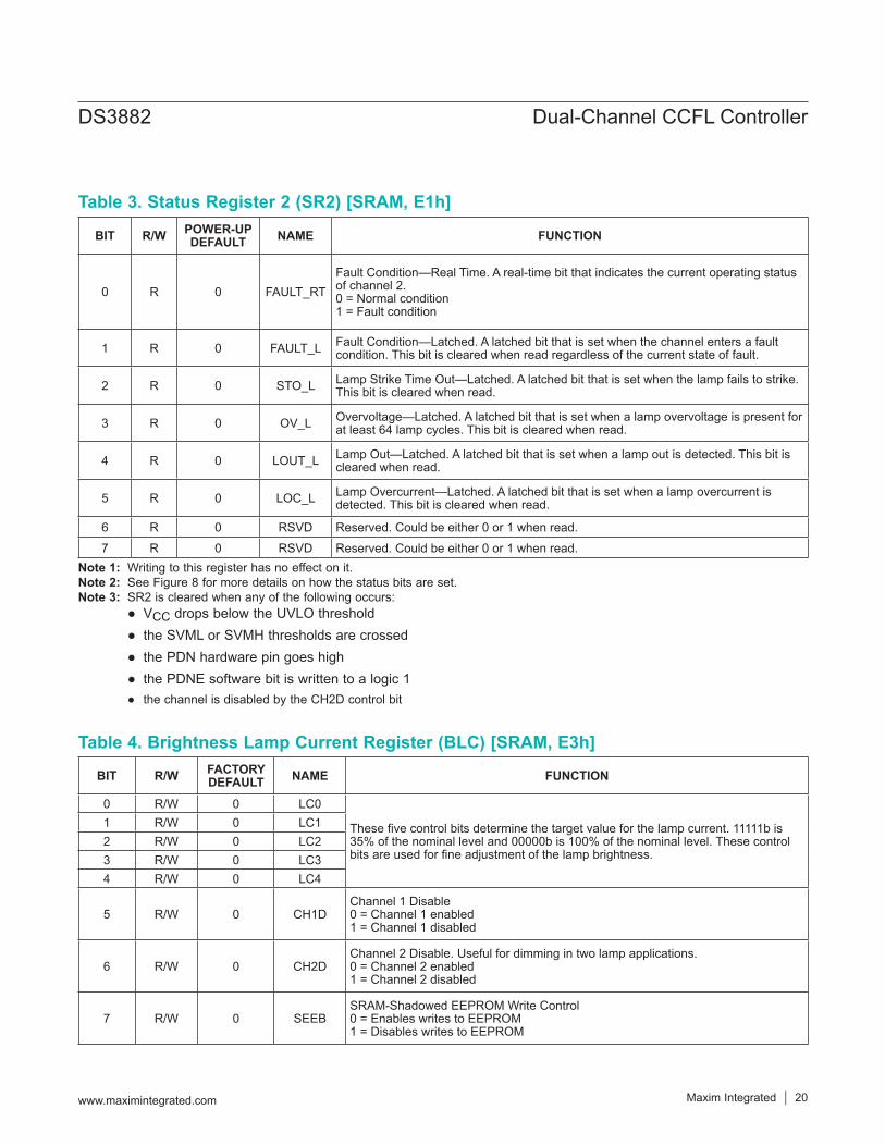
Table 4. Brightness Lamp Current Register (BLC) [SRAM, E3h]
Note 1: Writing to this register has no effect on it.Note 2: See Figure 8 for more details on how the status bits are set.Note 3: SR2 is cleared when any of the following occurs:
● VCC drops below the UVLO threshold ● the SVML or SVMH thresholds are crossed ● the PDN hardware pin goes high ● the PDNE software bit is written to a logic 1 ● the channel is disabled by the CH2D control bit
Table 3. Status Register 2 (SR2) [SRAM, E1h]
BIT R/W FACTORY DEFAULT NAME FUNCTION
0 R/W 0 LC0
These five control bits determine the target value for the lamp current. 11111b is 35% of the nominal level and 00000b is 100% of the nominal level. These control bits are used for fine adjustment of the lamp brightness.
1 R/W 0 LC12 R/W 0 LC23 R/W 0 LC34 R/W 0 LC4
5 R/W 0 CH1DChannel 1 Disable 0 = Channel 1 enabled 1 = Channel 1 disabled
6 R/W 0 CH2DChannel 2 Disable. Useful for dimming in two lamp applications. 0 = Channel 2 enabled 1 = Channel 2 disabled
7 R/W 0 SEEBSRAM-Shadowed EEPROM Write Control 0 = Enables writes to EEPROM 1 = Disables writes to EEPROM
BIT R/W POWER-UP DEFAULT NAME FUNCTION
0 R 0 FAULT_RTFault Condition—Real Time. A real-time bit that indicates the current operating status of channel 2. 0 = Normal condition 1 = Fault condition
1 R 0 FAULT_L Fault Condition—Latched. A latched bit that is set when the channel enters a fault condition. This bit is cleared when read regardless of the current state of fault.
2 R 0 STO_L Lamp Strike Time Out—Latched. A latched bit that is set when the lamp fails to strike. This bit is cleared when read.
3 R 0 OV_L Overvoltage—Latched. A latched bit that is set when a lamp overvoltage is present for at least 64 lamp cycles. This bit is cleared when read.
4 R 0 LOUT_L Lamp Out—Latched. A latched bit that is set when a lamp out is detected. This bit is cleared when read.
5 R 0 LOC_L Lamp Overcurrent—Latched. A latched bit that is set when a lamp overcurrent is detected. This bit is cleared when read.
6 R 0 RSVD Reserved. Could be either 0 or 1 when read.
7 R 0 RSVD Reserved. Could be either 0 or 1 when read.
www.maximintegrated.com Maxim Integrated │ 20
DS3882 Dual-Channel CCFL Controller
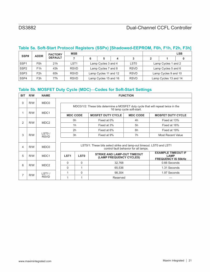
Table 5b. MOSFET Duty Cycle (MDC)—Codes for Soft-Start Settings
Table 5a. Soft-Start Protocol Registers (SSPx) [Shadowed-EEPROM, F0h, F1h, F2h, F3h]
BIT R/W NAME FUNCTION
0 R/W MDC0MDC0/1/2: These bits determine a MOSFET duty cycle that will repeat twice in the
16 lamp cycle soft-start.1 R/W MDC1
MDC CODE MOSFET DUTY CYCLE MDC CODE MOSFET DUTY CYCLE
2 R/W MDC20h Fixed at 0% 4h Fixed at 13%
1h Fixed at 3% 5h Fixed at 16%
3 R/W LST0 / RSVD
2h Fixed at 6% 6h Fixed at 19%
3h Fixed at 9% 7h Most Recent Value
4 R/W MDC0 LST0/1: These bits select strike and lamp-out timeout. LST0 and LST1 control fault behavior for all lamps.
5 R/W MDC1 LST1 LST0 STRIKE AND LAMP-OUT TIMEOUT (LAMP FREQUENCY CYCLES)
EXAMPLE TIMEOUT IF LAMP
FREQUENCY IS 50kHz
6 R/W MDC20 0 32,768 0.66 Seconds
0 1 65,536 1.31 Seconds
7 R/W LST1 / RSVD
1 0 98,304 1.97 Seconds
1 1 Reserved —
SSP# ADDR FACTORY DEFAULT
MSB LSB7 6 5 4 3 2 1 0
SSP1 F0h 21h LST1 Lamp Cycles 3 and 4 LST0 Lamp Cycles 1 and 2
SSP2 F1h 43h RSVD Lamp Cycles 7 and 8 RSVD Lamp Cycles 5 and 6
SSP3 F2h 65h RSVD Lamp Cycles 11 and 12 RSVD Lamp Cycles 9 and 10
SSP4 F3h 77h RSVD Lamp Cycles 15 and 16 RSVD Lamp Cycles 13 and 14
www.maximintegrated.com Maxim Integrated │ 21
DS3882 Dual-Channel CCFL Controller

Table 6. Control Register 1 (CR1) [Shadowed-EEPROM, F4h]
BIT R/W FACTORY DEFAULT NAME FUNCTION
0 R/W 0 LOCELamp Overcurrent Enable 0 = Lamp overcurrent detection disabled. 1 = Lamp overcurrent detection enabled.
1 R/W 0 POSCS
POSC Select. See POSCR0 and POSCR1 control bits in Control Register 2 to select the oscillator range. 0 = POSC input is connected with a resistor to ground to set the frequency of the internal PWM oscillator. 1 = POSC input is a 22.5Hz to 440Hz clock.
2 R/W 0 LFSSLamp Frequency Source Select 0 = Lamp frequency generated internally and sourced from the LSYNC output. 1 = Lamp frequency generated externally and supplied to the LSYNC input.
3 R/W 0 DPSSDPWM Signal Source Select 0 = DPWM signal generated internally and sourced from the PSYNC output. 1 = DPWM signal generated externally and supplied to the PSYNC input.
4 R/W 0 RGSORamp Generator Source Option 0 = Source DPWM at the PSYNC output. 1 = Source internal ramp generator at the PSYNC output.
5 R/W 0 ARDAutoretry Disable 0 = Autoretry function enabled. 1 = Autoretry function disabled.
6 R/W 0 FRSFault Response Select 0 = Disable only the malfunctioning channel. 1 = Disable both channels upon fault detection on any channel.
7 R/W 0 DPDDPWM Disable 0 = DPWM function enabled. 1 = DPWM function disabled.
www.maximintegrated.com Maxim Integrated │ 22
DS3882 Dual-Channel CCFL Controller

Table 7. Control Register 2 (CR2) [Shadowed-EEPROM, F5h]BIT R/W DEFAULT NAME FUNCTION
0 R/W 0 UMWPUser Memory Write Protect 0 = Write access blocked. 1 = Write access permitted.
1 R/W 0 POSCR0DPWM Oscillator Range Select. When using an external source for the dimming clock, these bits must be set to match the external oscillator’s frequency. When using a resistor to set the dimming frequency, these bits plus the external resistor control the frequency.
2 R/W 0 POSCR1
POSCR1 POSCR0 DIMMING CLOCK (DPWM) FREQUENCY RANGE (Hz) k (kW • kHz)
0 0 22.5 to 55.0 1
0 1 45 to 110 2
1 0 90 to 220 4
1 1 180 to 440 8
3 R/W 1 LSR0
Lamp Sample Rate Select. Determines the feedback sample rate of the LCM inputs.
LSR1 LSR0 SELECTED LAMP SAMPLE RATE
EXAMPLE SAMPLE RATE IF LAMP FREQUENCY IS
50kHz
0 0 4 Lamp Frequency Cycles 12,500Hz
4 R/W 0 LSR1
0 1 8 Lamp Frequency Cycles 6,250Hz
1 0 16 Lamp Frequency Cycles 3,125Hz
1 1 32 Lamp Frequency Cycles 1,563Hz
5 — 0 RSVD Reserved. This bit should be set to zero.
6 — 0 RSVD Reserved. This bit should be set to zero.
7 R/W 0 PDNEPower-Down. Logically ORed with the PDN pin. Setting this bit high resets the controller, clears the fault logic, and places the part in power-down mode. 0 = Normal. All circuitry is off, except I2C interface.
www.maximintegrated.com Maxim Integrated │ 23
DS3882 Dual-Channel CCFL Controller

Table 8. EMI Control Register (EMIC) [Shadowed-EEPROM, F6h]
BIT R/W FACTORY DEFAULT NAME FUNCTION
0 R/W 0 SS0
LAMP OSCILLATOR SPREAD-SPECTRUM MODULATION SELECTSS1 SS0 SELECTED LAMP FREQUENCY SPREAD
0 0 Spread-Spectrum Disabled
1 R/W 0 SS1
0 1 ±1.5%
1 0 ±3.0%
1 1 ±6.0%
2 R/W 0 SSMLamp Oscillator Spread-Spectrum Modulation Select 0 = Triangular modulation. 1 = Pseudorandom modulation.
3 — — RSVD Reserved. This bit should be set to zero.
4 R/W 0 STEPELamp Frequency Step Enable. Logically ORed with the Step Invoked. 0 = Lamp operates at nominal frequency. 1 = Frequency step invoked.
5 R/W 0 FS0
LAMP OSCILLATOR FREQUENCY STEP SELECT
FS2 FS1 FS0SELECTED LAMP
FREQUENCY STEP (SS0 = 0 AND SS1= 0)
SPREAD-SPECTRUM MODULATION RATE
(SS0 AND/OR SS1 = 1)
0 0 0 Step Up 1% Lamp Frequency x4
6 R/W 0 FS1
0 0 1 Step Up 2% Lamp Frequency x2
0 1 0 Step Up 3% Lamp Frequency x1
0 1 1 Step Up 4% Lamp Frequency x1/2
1 0 0 Step Down 1% Lamp Frequency x1/4
7 R/W 0 FS2
1 0 1 Step Down 2% Lamp Frequency x1/8
1 1 0 Step Down 3% Lamp Frequency x1/16
1 1 1 Step Down 4% Lamp Frequency x1/32
www.maximintegrated.com Maxim Integrated │ 24
DS3882 Dual-Channel CCFL Controller
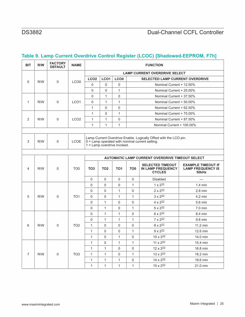
Table 9. Lamp Current Overdrive Control Register (LCOC) [Shadowed-EEPROM, F7h]
BIT R/W FACTORY DEFAULT NAME FUNCTION
0 R/W 0 LCO0
LAMP CURRENT OVERDRIVE SELECTLCO2 LCO1 LCO0 SELECTED LAMP CURRENT OVERDRIVE
0 0 0 Nominal Current + 12.50%
0 0 1 Nominal Current + 25.00%
1 R/W 0 LCO1
0 1 0 Nominal Current + 37.50%
0 1 1 Nominal Current + 50.00%
1 0 0 Nominal Current + 62.50%
2 R/W 0 LCO2
1 0 1 Nominal Current + 75.00%
1 1 0 Nominal Current + 87.50%
1 1 1 Nominal Current + 100.00%
3 R/W 0 LCOELamp Current Overdrive Enable. Logically ORed with the LCO pin. 0 = Lamp operated with nominal current setting. 1 = Lamp overdrive invoked.
4 R/W 0 TO0
AUTOMATIC LAMP CURRENT OVERDRIVE TIMEOUT SELECT
TO3 TO2 TO1 TO0SELECTED TIMEOUT IN LAMP FREQUENCY
CYCLES
EXAMPLE TIMEOUT IF LAMP FREQUENCY IS
50kHz
0 0 0 0 Disabled —
5 R/W 0 TO1
0 0 0 1 1 x 222 1.4 min
0 0 1 0 2 x 222 2.8 min
0 0 1 1 3 x 222 4.2 min
0 1 0 0 4 x 222 5.6 min
0 1 0 1 5 x 222 7.0 min
6 R/W 0 TO2
0 1 1 0 6 x 222 8.4 min
0 1 1 1 7 x 222 9.8 min
1 0 0 0 8 x 222 11.2 min
1 0 0 1 9 x 222 12.6 min
1 0 1 0 10 x 222 14.0 min
7 R/W 0 TO3
1 0 1 1 11 x 222 15.4 min
1 1 0 0 12 x 222 16.8 min
1 1 0 1 13 x 222 18.2 min
1 1 1 0 14 x 222 19.6 min
1 1 1 1 15 x 222 21.0 min
www.maximintegrated.com Maxim Integrated │ 25
DS3882 Dual-Channel CCFL Controller
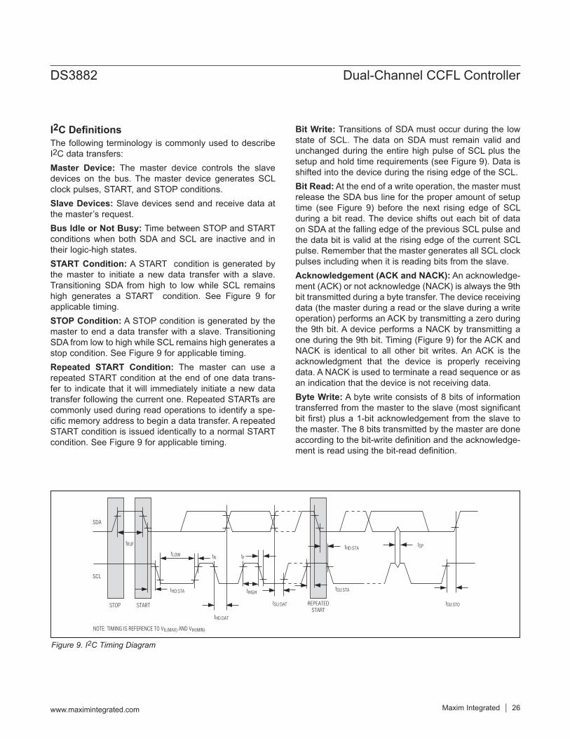
I2C DefinitionsThe following terminology is commonly used to describe I2C data transfers:Master Device: The master device controls the slave devices on the bus. The master device generates SCL clock pulses, START, and STOP conditions.Slave Devices: Slave devices send and receive data at the master’s request.Bus Idle or Not Busy: Time between STOP and START conditions when both SDA and SCL are inactive and in their logic-high states.START Condition: A START condition is generated by the master to initiate a new data transfer with a slave. Transitioning SDA from high to low while SCL remains high generates a START condition. See Figure 9 for applicable timing.STOP Condition: A STOP condition is generated by the master to end a data transfer with a slave. Transitioning SDA from low to high while SCL remains high generates a stop condition. See Figure 9 for applicable timing.Repeated START Condition: The master can use a repeated START condition at the end of one data trans-fer to indicate that it will immediately initiate a new data transfer following the current one. Repeated STARTs are commonly used during read operations to identify a spe-cific memory address to begin a data transfer. A repeated START condition is issued identically to a normal START condition. See Figure 9 for applicable timing.
Bit Write: Transitions of SDA must occur during the low state of SCL. The data on SDA must remain valid and unchanged during the entire high pulse of SCL plus the setup and hold time requirements (see Figure 9). Data is shifted into the device during the rising edge of the SCL.Bit Read: At the end of a write operation, the master must release the SDA bus line for the proper amount of setup time (see Figure 9) before the next rising edge of SCL during a bit read. The device shifts out each bit of data on SDA at the falling edge of the previous SCL pulse and the data bit is valid at the rising edge of the current SCL pulse. Remember that the master generates all SCL clock pulses including when it is reading bits from the slave.Acknowledgement (ACK and NACK): An acknowledge-ment (ACK) or not acknowledge (NACK) is always the 9th bit transmitted during a byte transfer. The device receiving data (the master during a read or the slave during a write operation) performs an ACK by transmitting a zero during the 9th bit. A device performs a NACK by transmitting a one during the 9th bit. Timing (Figure 9) for the ACK and NACK is identical to all other bit writes. An ACK is the acknowledgment that the device is properly receiving data. A NACK is used to terminate a read sequence or as an indication that the device is not receiving data.Byte Write: A byte write consists of 8 bits of information transferred from the master to the slave (most significant bit first) plus a 1-bit acknowledgement from the slave to the master. The 8 bits transmitted by the master are done according to the bit-write definition and the acknowledge-ment is read using the bit-read definition.
Figure 9. I2C Timing Diagram
SDA
SCL
tHD:STA
tLOW
tHIGH
tR tF
tBUF
tHD:DAT
tSU:DAT REPEATEDSTART
tSU:STA
tHD:STA
tSU:STO
tSP
STOP
NOTE: TIMING IS REFERENCE TO VIL(MAX) AND VIH(MIN).
START
www.maximintegrated.com Maxim Integrated │ 26
DS3882 Dual-Channel CCFL Controller

Byte Read: A byte read is an 8-bit information transfer from the slave to the master plus a 1-bit ACK or NACK from the master to the slave. The 8 bits of information that are transferred (most significant bit first) from the slave to the master are read by the master using the bit read definition above, and the master transmits an ACK using the bit write definition to receive additional data bytes. The master must NACK the last byte read to ter-minate communication so the slave will return control of SDA to the master.Slave Address Byte: Each slave on the I2C bus responds to a slave addressing byte sent immediately following a START condition. The slave address byte (Figure 10) contains the slave address in the most significant 7 bits and the R/W bit in the least significant bit. The DS3882’s slave address is 10100A1A0 (bina-ry), where A0 and A1 are the values of the address pins (A0 and A1). The address pin allows the device to respond to one of four possible slave addresses. By writing the correct slave address with R/W = 0, the master indicates it will write data to the slave. If R/W = 1, the master will read data from the slave. If an incorrect slave address is written, the DS3882 will assume the master is communicating with another I2C device and ignore the communications until the next START condi-tion is sent.Memory Address: During an I2C write operation, the master must transmit a memory address to identify the memory location where the slave is to store the data. The memory address is always the second byte transmit-ted during a write operation following the slave address byte.
I2C CommunicationWriting a Data Byte to a Slave: The master must gen-erate a START condition, write the slave address byte (R/W = 0), write the memory address, write the byte of data, and generate a STOP condition. Remember the master must read the slave’s acknowledgement during all byte write operations. See Figure 11 for more detail.
Acknowledge Polling: Any time EEPROM is written, the DS3882 requires the EEPROM write time (tW) after the STOP condition to write the contents to EEPROM. During the EEPROM write time, the DS3882 will not acknowl-edge its slave address because it is busy. It is possible to take advantage of that phenomenon by repeatedly addressing the DS3882, which allows the next byte of data to be written as soon as the DS3882 is ready to receive the data. The alternative to acknowledge polling is to wait for a maximum period of tW to elapse before attempting to write again to the DS3882.EEPROM Write Cycles: The number of times the DS3882’s EEPROM can be written before it fails is speci-fied in the Nonvolatile Memory Characteristics table. This specification is shown at the worst-case write tempera-ture. The DS3882 is typically capable of handling many additional write cycles when the writes are performed at room temperature.Reading a Data Byte from a Slave: To read a single byte from the slave the master generates a START con-dition, writes the slave address byte with R/W = 0, writes the memory address, generates a repeated START con-dition, writes the slave address with R/W = 1, reads the data byte with a NACK to indicate the end of the transfer, and generates a STOP condition. See Figure 11 for more detail.
Figure 10. DS3882’s Slave Address Byte
7-BIT SLAVE ADDRESS
MOSTSIGNIFICANT BIT
A1, A0 PIN VALUE DETERMINESREAD OR WRITE
R/W1 0 1 0 0 A1 A0
www.maximintegrated.com Maxim Integrated │ 27
DS3882 Dual-Channel CCFL Controller

Applications InformationAddressing Multiple DS3882s On a Common I2C BusEach DS3882 responds to one of four possible slave addresses based on the state of the address input pins (A0 and A1). For information about device addressing, see the I2C Communication section.
Setting the RMS Lamp CurrentResistor R7 and R8 in the Typical Operating Circuit set the lamp current. R7 and R8 = 140W corresponds to a 5mARMS lamp current as long as the current waveform is approximately sinusoidal. The formula to determine the resistor value for a given sinusoidal lamp current is:
7 / 8LAMP(RMS)
1R I x 2
=
Component SelectionExternal component selection has a large impact on the overall system performance and cost. The two most important external components are the transformers and n-channel MOSFETs.The transformer should be able to operate in the 40kHz to 80kHz frequency range of the DS3882, and the turns
ratio should be selected so the MOSFET drivers run at 28% to 35% duty cycle during steady state operation. The transformer must be able to withstand the high open-cir-cuit voltage that is used to strike the lamp. Additionally, its primary/secondary resistance and inductance char-acteristics must be considered because they contribute significantly to determining the efficiency and transient response of the system. Table 10 shows a transformer specification that has been used for a 12V inverter supply, 438mm x 2.2mm lamp design.The n-channel MOSFET must have a threshold voltage that is low enough to work with logic-level signals, a low on-resistance to maximize efficiency and limit the n-channel MOSFET’s power dissipation, and a break-down voltage high enough to handle the transient. The breakdown voltage should be a minimum of 3x the invert-er voltage supply. Additionally, the total gate charge must be less than QG, which is specified in the Recommended Operating Conditions table. These specifications are eas-ily met by many of the dual n-channel MOSFETs now available in 8-pin SO packages.Table 11 lists suggested values for the external resistors and capacitors used in the Typical Operating Circuit.
Figure 11. I2C Communications Examples
X X X X X X X X
1 0 1 0 A0 0A10
COMMUNICATIONS KEY
WRITE A SINGLE BYTE
8-BITS ADDRESS OR DATA
WHITE BOXES INDICATE THE MASTER IS CONTROLLING SDA
NOTES
2) THE FIRST BYTE SENT AFTER A START CONDITION IS ALWAYS THE SLAVE ADDRESS FOLLOWED BY THE READ/WRITE BIT.
SHADED BOXES INDICATE THE SLAVE IS CONTROLLING SDA
START ACK
NOTACK
S
S A A A PDATAMEMORY ADDRESS
1 0 1 0 A0 0A10 1 0 1 0 A0 1A10
READ A SINGLE BYTE
S A A SR A N PDATAMEMORY ADDRESS
A
P N
SR
STOP
REPEATEDSTART
1) ALL BYTES ARE SENT MOST SIGNIFICANT BIT FIRST.
www.maximintegrated.com Maxim Integrated │ 28
DS3882 Dual-Channel CCFL Controller
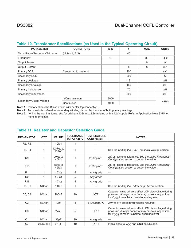
Table 11. Resistor and Capacitor Selection Guide
Note 1: Primary should be Bifilar wound with center tap connection.Note 2: Turns ratio is defined as secondary winding divided by the sum of both primary windings.Note 3: 40:1 is the nominal turns ratio for driving a 438mm x 2.2mm lamp with a 12V supply. Refer to Application Note 3375 for
more information.
Table 10. Transformer Specifications (as Used in the Typical Operating Circuit)
DESIGNATOR QTY VALUE TOLERANCE (%) AT +25°C
TEMPERATURE COEFFICIENT NOTES
R5, R6 1 10kW 1 — —
R3, R4 1 12.5kW to 105kW 1 — See the Setting the SVM Threshold Voltage section.
R9 1 20kW to 40kW 1 ≤153ppm/°C 2% or less total tolerance. See the Lamp Frequency
Configuration section to determine value.
R10 1 18kW to 45kW 1 ≤153ppm/°C 2% or less total tolerance. See the Lamp Frequency
Configuration section to determine value.
R1 1 4.7kW 5 Any grade —
R2 1 4.7kW 5 Any grade —
R11 1 4.7kW 5 Any grade —
R7, R8 1/Chan 140W 1 — See the Setting the RMS Lamp Current section.
C6, C8 1/Chan 100nF 10 X7RCapacitor value will also affect LCM bias voltage during power-up. A larger capacitor may cause a longer time for VDCB to reach its normal operating level.
C2 1/Chan 10pF 5 ±1000ppm/°C 2kV to 4kV breakdown voltage required.
C3 1/Chan 27nF 5 X7RCapacitor value will also affect LCM bias voltage during power-up. A larger capacitor may cause a longer time for VDCB to reach its normal operating level.
C1 1/Chan 33µF 20 Any grade —
C7 2/DS3882 0.1µF 10 X7R Place close to VCC and GND on DS3882.
PARAMETER CONDITIONS MIN TYP MAX UNITSTurns Ratio (Secondary/Primary) (Notes 1, 2, 3) 40
Frequency 40 80 kHz
Output Power 6 W
Output Current 5 8 mA
Primary DCR Center tap to one end 200 mW
Secondary DCR 500 W
Primary Leakage 12 µH
Secondary Leakage 185 mH
Primary Inductance 70 µH
Secondary Inductance 500 mH
Secondary Output Voltage100ms minimum 2000
VRMSContinuous 1000
www.maximintegrated.com Maxim Integrated │ 29
DS3882 Dual-Channel CCFL Controller

Power-Supply DecouplingTo achieve best results, it is highly recommended that a decoupling capacitor is used on the IC power-supply pin. Typical values of decoupling capacitors are 0.01µF or 0.1µF. Use a high-quality, ceramic, surface-mount capaci-tor, and mount it as close as possible to the VCC and GND pins of the IC to minimize lead inductance. PACKAGE
TYPEPACKAGE
CODEOUTLINE
NO.LAND
PATTERN NO.
28 TSSOP(173 mils) U28+2 21-0066 90-0171
INVERTER SUPPLYVOLTAGE (VINV)
(8V TO 16V)
GA1
LAMP CURRENT MONITOR
CCFL LAMP
GB1
OVD1
VCC
VCCVCC
VCC
BRIGHT
SVMH
LAMP BRIGHTNESS
TRANSFORMERDUAL POWERMOSFET
DEVICESUPPLY VOLTAGE
(5V 5%)
OVERVOLTAGE DETECTION
LCM1
GND
LAMP FREQUENCYINPUT/OUTPUT
LSYNC
SCL
SDAI2C
CONFIGURATIONAND CONTROL PORT
FAULT
PSYNCDPWM SIGNALINPUT/OUTPUT
LOSC
POSC
LCO
PDNLAMP ON/OFF
LAMP CURRENTOVERDRIVE ENABLE
SVMLA0
A1
HARDWARECONTROL
STEP LAMPFREQUENCY
STEP
GND_S
R1 R2
R7
R9 R10
C2
C3
C7
R11
C8
R3 R4
R5 R6
C1
GA2
LAMP CURRENT MONITOR
CCFL LAMP
GB2
OVD2
TRANSFORMERDUAL POWERMOSFET OVERVOLTAGE DETECTION
LCM2
R8
C4
C5
C6
DS3882
www.maximintegrated.com Maxim Integrated │ 30
DS3882 Dual-Channel CCFL Controller
Package InformationFor the latest package outline information and land patterns (footprints), go to www.maximintegrated.com/packages. Note that a “+”, “#”, or “-” in the package code indicates RoHS status only. Package drawings may show a different suffix character, but the drawing pertains to the package regardless of RoHS status.
Chip InformationSUBSTRATE CONNECTED TO GROUND
Typical Operating Circuit
REVISION NUMBER
REVISION DATE DESCRIPTION PAGES
CHANGED
0 3/06 Initial release —
1 8/07 Updated Table 5b to change bit 7 LST[1:0] at 1:1 from 131,072 lamp frequency cycles to reserved 21
2 12/10Updated the Ordering Information table part numbers; added the continuous power dissipation numbers for a single-layer board and the lead and soldering temperature information to the Absolute Maximum Ratings section; added the Package Information table
1, 2, 30
3 4/15 Removed references to “Automotive” from the title, General Description, Applications, and Features sections 1
Maxim Integrated cannot assume responsibility for use of any circuitry other than circuitry entirely embodied in a Maxim Integrated product. No circuit patent licenses are implied. Maxim Integrated reserves the right to change the circuitry and specifications without notice at any time. The parametric values (min and max limits) shown in the Electrical Characteristics table are guaranteed. Other parametric values quoted in this data sheet are provided for guidance.
Maxim Integrated and the Maxim Integrated logo are trademarks of Maxim Integrated Products, Inc. © 2015 Maxim Integrated Products, Inc. │ 31
DS3882 Dual-Channel CCFL Controller
Revision History
For pricing, delivery, and ordering information, please contact Maxim Direct at 1-888-629-4642, or visit Maxim Integrated’s website at www.maximintegrated.com.