Embed Size (px)
Citation preview

DOCTOR OF PHILOSOPHY
Development and testing of thin photocatalyst films
McNeill, Aaron
Award date:2021
Awarding institution:Queen's University Belfast
Link to publication
Terms of useAll those accessing thesis content in Queen’s University Belfast Research Portal are subject to the following terms and conditions of use
• Copyright is subject to the Copyright, Designs and Patent Act 1988, or as modified by any successor legislation • Copyright and moral rights for thesis content are retained by the author and/or other copyright owners • A copy of a thesis may be downloaded for personal non-commercial research/study without the need for permission or charge • Distribution or reproduction of thesis content in any format is not permitted without the permission of the copyright holder • When citing this work, full bibliographic details should be supplied, including the author, title, awarding institution and date of thesis
Take down policyA thesis can be removed from the Research Portal if there has been a breach of copyright, or a similarly robust reason.If you believe this document breaches copyright, or there is sufficient cause to take down, please contact us, citing details. Email:[email protected]
Supplementary materialsWhere possible, we endeavour to provide supplementary materials to theses. This may include video, audio and other types of files. Weendeavour to capture all content and upload as part of the Pure record for each thesis.Note, it may not be possible in all instances to convert analogue formats to usable digital formats for some supplementary materials. Weexercise best efforts on our behalf and, in such instances, encourage the individual to consult the physical thesis for further information.
Download date: 20. Jan. 2022

Queen’s University Belfast
School of Chemistry & Chemical Engineering
Development and Testing of
Thin Photocatalyst Films
By
Aaron McNeill
A thesis presented in fulfilment for the requirements for the degree of
Doctor of Philosophy
2021

i
Abstract
This thesis details the development of surface-exposed nanoparticle (SEN)
films made from titanium dioxide (TiO2) and cadmium sulfide (CdS)
nanoparticles, as well as their characterisation and testing for photocatalytic
activity by using a variety of known photocatalytic reactions and techniques.
A TiO2-SEN film is detailed, based on the formation of ion-pairs formed
between TiO2 P25 nanoparticles in an acidic dispersion, and an anionic
lipophilic promoter, which find themselves most stable in a water-organic
interface. These interfacial films are then captured in situ by polymer film
formation as the solvent evaporates. The photoactivity of the film is then
quantified using the oxidations of 4-chlorophenol and methylene blue, as well
as the reductions of methylene blue and resazurin, in solution and ink forms.
The photoactivity of TiO2-SEN film is measured against Pilkington ActivTM
glass for each of these reactions, which is a commercial product that has a
TiO2 film analogous to the films made in this work.
A SEN film from a synthesised CdS colloid is also described, highlighting the
ease and versatility of the film synthesis method. These films are found to
perform well in photocatalytic reactions suitable for CdS, including the
reduction of dissolved oxygen, methyl orange, crystal violet and methyl
viologen, as well as the reduction of water to create hydrogen when in the
presence of a platinum co-catalyst. Methods devised to improve robustness of
these films are described, including the 3D-printing of a transparent backing
layer and ironing on the films to various plastics and fabrics, both using heat
transfer. These methods vastly improve the ease of handling of the SEN films
without being at the cost of photoactivity.
The development of a photoinduced absorption spectroscopy (PIAS) setup is
described, as well as its use to investigate the photoreduction of oxygen by
monitoring the formation and decay of transients associated with
photogeneration of electrons in CdS paste films, TiO2 paste films and TiO2-
SEN films. These results are also compared against results of steady-state
oxygen photoreduction by extracting constants to describe the dependence of
formation and decay rate of electrons on the level of oxygen in solution.

ii
Acknowledgements
There are several people that I must thank for being there for me throughout
the gruelling process that is a PhD. I must first thank my supervisor Professor
Andrew Mills for helping me to fit together all the pieces of my work into our
various publications and ultimately this thesis. Also, thank you for being patient
with me when I misread equations and constants, more times than I am willing
to admit.
I would also like to thank Dr Chris O’Rourke, who has been my office mate
throughout the entire course of my PhD, and for the last year or two, my fellow
cave-dweller in the time singularity that is the laser lab. You always been there
for me whether I needed any assistance setting up experiments, a second
opinion, or simply a chat about anything and, quite possibly, everything. I
couldn’t have done this without you.
I’d also like to thank an expansive list of researchers in the building, both past
and present. To my former gym buddies Dan, Con and Dili, to lunch buddies
Hannah and Michael, and to unspecified activity buddies (in no particular
order): Rachel, James, Ri, Joe, Luke, Michelle, Rose, Sofia, Soo-Keun,
Nathan and David. I would say that I’m sorry for talking so much, but I think
we all know that would be a lie. My thanks also go to my second supervisor
Professor Steven Bell and his group, in particular Yikai, Ziwei and Xinyuan, for
all their help and reminding me that there is indeed life outside the group.
As treacherous as dealing with my nonsense likely is, all sympathy should be
directed to my brother Andrew, who has had to put up with my meddlesome
existence for 26 long years. From being forever second place to me in every
game under the sun (citation needed), to reciting our own ridiculous songs and
tales which should never see the light of day if we wish to ever be taken
seriously again, we have constantly enabled each other’s absurdity - which I
suspect will become our own undoing. Even though you were rude enough to
leave me for Arizona, I still miss you as we haven’t seen each other in over a
year for obvious travel restrictive reasons. When the dust settles, let me see
you nod your head, because I’m coming. Whether you like it or not. And yes,

iii
that’s the reference I’m choosing to make. You continue to be the smartest
person I know, and I doubt that will ever change.
Of course, my brother can’t be solely to blame for me being the way I am – my
parents must take some of the responsibility also. They have taught me the
importance of persistence and hard work, and also vehemently to know the
difference between they’re, their and there. That being said, their the best
source of love and support out they’re, and all there sacrifices to raise both me
and my brother will be forever appreciated. I hope reading the grammar of that
sentence was as painful for you to read as it was for me to write.
Last, and most certainly least, I would like to thank my best friend and
roommate Ryan. We met through bizarre chance, and I dread to think where I
would have ended up if we hadn’t. You’ve been there for me countless times
to make me feel special during my ‘oof’ moments when I’ve been having
figurative trouble with the trolley. I can only hope to repay you by continuing to
facilitate your various obsessions, starting with the many references here, and
from now on, you’ll never see it coming. Just please, no more Forces. In spite
of all of this, you are rotted, infuriating and rude, and I wouldn’t have you any
other way - that’s a fact. And facts are facts.
– Bruce Springsteen

iv
Table of Contents
Abstract i
Acknowledgements ii
Table of Contents iv
Abbreviations viii
Table of Figures x
Chapter 1: Introduction 1
1.1. Semiconductor photocatalysis 2
1.1.1. Titanium dioxide 5
1.1.2. TiO2 applications 6
1.1.3. Cadmium sulfide 9
1.1.4. CdS applications 11
1.1.5. Quantification of photocatalytic activity 14
1.1.6. Photoinduced absorption spectroscopy (PIAS) 16
1.2. Thin films of TiO2 and CdS 21
1.3. MeLLFs and SEN films 23
1.3.1. Theory of MeLLFs 23
1.3.2. Silver MeLLFs 25
1.3.3. Gold MeLLFs 27
1.3.4. Non-metal liquid-like films 28
1.3.5. MeLLF deposition 29
1.3.6. Surface-exposed nanoparticle (SEN) films 30
1.4. Aims and objectives 31
1.5. References 32
Chapter 2: Techniques and Instrumentation 37
2.1. Materials 38
2.2. Instrumentation 38
2.2.1. UV–vis spectroscopy 38
2.2.2. Scanning electron microscopy 39
2.2.3. Transmission electron microscopy 41
2.2.4. Atomic force microscopy 41
2.2.5. Powder X-ray diffraction 42

v
2.2.6. Gas chromatography 43
2.2.7. Fourier transform infrared spectroscopy 45
2.2.8. Photoinduced absorption spectroscopy 45
2.2.9. Irradiation sources 48
2.3. Synthesis of colloids and dispersions 49
2.3.1. TiO2 dispersion 49
2.3.2. Cadmium sulfide colloid 50
2.3.3. CdS and TiO2 P25 paste 50
2.3.4. Platinum colloid 51
2.4. Film production 51
2.4.1. TiO2- and CdS-SEN films 51
2.4.2. 3D-printed support film 53
2.4.3. CdS and TiO2 paste films 54
2.5. References 55
Chapter 3: Production and Testing of TiO2-SEN Films 56
3.1. Introduction 57
3.2. Experimental 58
3.2.1. TiO2 dispersion 58
3.2.2. TiO2 surface-exposed nanoparticle (TiO2-SEN) films 58
3.2.3. Aqueous solution photocatalytic oxidation and reduction tests 60
3.2.4. Ink film photocatalytic tests 61
3.3. Results and discussion 61
3.3.1. Characterisation 61
3.3.2. 4-Chlorophenol degradation test 65
3.3.3. Methylene blue ISO test 68
3.3.4. Rz/glycerol photocatalytic test 70
3.3.5. Rz ink test 72
3.3.6. MB ink test 74
3.4. Conclusions 75
3.5. References 76
Chapter 4: Production and Testing of CdS-SEN Films 78
4.1. Introduction 79

vi
4.2. Materials and methods 81
4.2.1. Materials 81
4.2.2. Cadmium sulfide colloid 81
4.2.3. TiO2 dispersion 82
4.2.4. Platinum colloid 82
4.2.5. CdS- and TiO2-SEN film production 83
4.2.6. 3D-printed backing for photocatalyst-SEN (PC-SEN) films 84
4.2.7. Photocatalysed reduction of O2 84
4.2.8. Photocatalysed reduction of dyes 85
4.2.9. Photocatalysed reduction of MV and H2 generation in solution 85
4.2.10. Instrumentation 86
4.3. Results and discussion 87
4.3.1. CdS-SEN film characterisation 87
4.3.2. Photocatalysed reduction of O2 89
4.3.3. Photocatalysed reductive bleaching of MO and CV 91
4.3.4. Reduction of MV2+ and H2 generation in solution with Pt 95
4.4. Conclusion 98
4.5. References 99
Chapter 5: Heat-Transfer (‘iron-on’) Photocatalytic Films 101
5.1. Introduction 102
5.2. Experimental 103
5.2.1. CdS and TiO2 colloid and film synthesis 103
5.2.2. Photocatalytic reductions and oxidations 106
5.3. Results and discussion 107
5.3.1. Photoreduction of methyl orange (MO), methyl viologen and water 107
5.3.2. Photocatalysed oxidation of methylene blue and NO 110
5.4. Conclusions 113
5.5. References 114
Chapter 6: Photoinduced Absorption Spectroscopy of CdS Films 116
6.1. Introduction 117
6.2. Experimental 119
6.2.1. CdS paste film synthesis 119

vii
6.2.2. Photoinduced absorption spectroscopy (PIAS) 120
6.2.3. Steady state photoreduction of O2 measurements 120
6.3. Results and discussion 121
6.4. Conclusion 127
6.5. References 128
Chapter 7: Photoinduced Absorption Spectroscopy of TiO2 Films 130
7.1. Introduction 131
7.2. Experimental 133
7.2.1. TiO2 paste film and TiO2-SEN film synthesis 133
7.2.2. Photoinduced absorption spectroscopy (PIAS) 134
7.2.3. Steady state photoreduction of O2 measurements 135
7.3. Results and discussion 135
7.4. Conclusion 145
7.5. References 145
Chapter 8: Conclusions & Future Work 146
8.1. Summary 147
8.2. TiO2-SEN films 147
8.3. CdS-SEN films 148
8.4. Mounting films 149
8.5. Photoinduced absorption spectroscopy (PIAS) 150
8.6. References 151
Appendix A: Papers published & conferences attended 152

viii
Abbreviations
4-CP 4-Chlorophenol
AA Ascorbic acid
Abs Absorption
ΔAbs Absorption change
ΔAbsss Steady-state absorption change
AFM Atomic Force Microscopy
BLB Blacklight Blue
BRSC Borohydride-reduced silver colloid
Cot Cotton
CRGC Citrate-reduced gold colloid
CRSC Citrate-reduced silver colloid
CV Crystal violet
DAQ Data Acquisition
DCM Dichloromethane
e- Photogenerated electron
EDTA Ethylenediaminetetraacetate
FTIR Fourier Transform Infrared
GC Gas Chromatography
h+ Photogenerated hole
HEC Hydroxyethylcellulose
HOMO Highest Occupied Molecular Orbital
ISO International Organization for Standardization
Jss Steady-state Photocurrent
λm Monitoring beam wavelength
LED Light Emitting Diode
LUMO Lowest Unoccupied Molecular Orbital
MB Methylene blue
MeLLF Metal Liquid-Like Film
MO Methyl orange
MV Methyl viologen
NaA Sodium ascorbate
NHE Normal Hydrogen Electrode
OD Optical Density

ix
PC Photocatalyst
PCO Photocatalytic Oxidation
PET Polyethylene terephthalate
PIAS Photoinduced Absorption Spectroscopy
PLA Polylactic acid
PP Polypropylene
PS Polystyrene
PS20 Polysorbate 20
PSH Photoinduced Superhydrophilicity
PTA Phase Transfer Agent
PVC Poly(vinyl chloride)
QD Quantum Dot
ρ Irradiance
Rf Resorufin
ROS Reactive Oxygen Species
Rz Resazurin
SC Semiconductor
SEA Sacrificial Electron Acceptor
SED Sacrificial Electron Donor
SEM Scanning Electron Microscopy
SEN Surface Exposed Nanoparticle
SERS Surface-Enhanced Raman Spectroscopy
TAS Transient Absorption Spectroscopy
TBA Tetrabutylammonium
TC Transient Photocurrent
TEM Transmission Electron Microscopy
TPB Tetraphenylborate
UV(A) Ultraviolet A
UV-vis Ultraviolet-visible
VOC Volatile Organic Compounds
XRD X-Ray Diffraction

x
Table of Figures
Figure 1.1. Illustration of the major processes of semiconductor photocatalysis on a semiconductor particle upon photoexcitation. Process I shows a photogenerated electron reducing an electron acceptor (A), process II shows a photogenerated hole oxidising an electron donor D, and process III is the recombination of an electron-hole pair to release heat.
3
Figure 1.2. Illustration of changes in the electronic structure of a semiconductor with increasing number of units (N) which bring about a surpassable band gap.
4
Figure 1.3. Positions of valence bands and conduction bands of common semiconductor photocatalysts vs. NHE at pH 0 and pH 7. Dashed lines at 0 V and 1.23 V vs. NHE at pH 0 corresponds to hydrogen and oxygen evolution potentials, respectively [2].
4
Figure 1.4. Unit cell structures of anatase and rutile TiO2. Grey and red balls represent titanium and oxygen atoms, respectively.
5
Figure 1.5. Illustration of the main processes of photomineralisation of organic pollutants by oxygen with titania semiconductor acting as a photocatalyst.
6
Figure 1.6. Illustration of the main processes of photoinduced superhydrophilicity on a titanium dioxide surface.
8
Figure 1.7. Illustration of the process in which a pane of glass with a TiO2 layer on top exhibits self-cleaning.
9
Figure 1.8. Unit cell structures of hawleyite (sphalerite structure) and greenockite (wurtzite structure). Grey and yellow balls represent cadmium and sulfur atoms, respectively.
10
Figure 1.9. Photoinduced absorption spectra of a solgel TiO2 film when irradiated with a 337 nm laser in the presence of methanol. Data extracted from Tang et al. [89].
17
Figure 1.10. Typical photoinduced absorption observed in a CdS colloid in the presence of hexametaphosphate when subjected to a 10 µs photoflash (λ > 300 nm). Data extracted from Darwent et al. [66].
20
Figure 1.11. Diagram illustrating the Burstein-Moss effect to increase the observed band gap in a photosensitised semiconductor.
21
Figure 1.12. Simplified representation of the position of particles of varying levels of hydrophobicity/philicity in a planar liquid-liquid interface, with contact angle (θ) shown.
24
Figure 1.13. General behaviour of negatively charged nanoparticles with aqueous counterions (e.g. Na+, blue) in a biphasic system before and after adding an organic-soluble cationic promoter (e.g. tetrabutylammonium, purple).
25
Figure 1.14. SEM images of monolayers of (A) P25 TiO2 particles and (B) SiO2 particles. Scale bars represent 1 µm. From Ref [118].
29
Figure 1.15. Illustration showing the steps behind MeLLF formation with negatively charged nanoparticles using tetrabutylammonium (Q+) as a promoter, with polymer dissolved in the DCM phase, and allowing this phase to evaporate, capturing the nanoparticles in the polystyrene (PS) film.
31

xi
Figure 2.1. A typical UV–vis spectrum measured with a Cary 60 UV–vis spectrophotometer of a 10 µM aqueous solution of methylene blue in a 1 cm cuvette, with maximum wavelength of absorption (λmax) and the absorbance value taken to compensate for vessel walls and solvent absorbances (ΔAbs).
39
Figure 2.2. Scanning electron micrograph of the surface of self-cleaning glass (Pilkington Activ™) as a typical example of an SEM taken with this instrument.
40
Figure 2.3. Example transmission electron micrograph of a drop-casted dispersion of synthesised cadmium sulfide nanoparticles on holey carbon.
41
Figure 2.4. A three-dimensional map of the surface of a 1x1 µm area of the TiO2 layer on self-cleaning glass (Pilkington Activ™) acquired using atomic force microscopy.
42
Figure 2.5. A typical XRD profile of a sample of TiO2 P25 powder. Peaks corresponding to anatase (*) and rutile (▲) can be easily distinguished.
43
Figure 2.6. An example gas chromatograph of hydrogen acquired from the gas chromatography set-up mentioned above.
44
Figure 2.7. Typical infrared spectrum with the instrument mentioned above, of a polystyrene film on a calcium fluoride disc.
45
Figure 2.8. Schematic of the PIAS setup used in this work. Cell is shown in a larger scale for clarity.
47
Figure 2.9. 3D model of the cell used to hold samples and electrodes in solution for PIAS.
47
Figure 2.10. Example photoinduced absorption spectroscopy trace acquired using the aforementioned setup of a TiO2 P25 paste film in an SED-containing aqueous solution (Na2EDTA) with an 850 nm monitoring beam and UV LED operating.
48
Figure 2.11. Emission profiles of the 365 nm (black line), 420 nm (violet line) and 595 nm (orange line) LEDs, each at irradiance 10 mW cm-2.
49
Figure 2.12. Digital image of an acidic 1 g L-1 P25 dispersion after centrifugation (right), and a dispersion of the same amount of TiO2 of a centrifuged dispersion (67 mg L-1) with P25 powder (left).
50
Figure 2.13. Digital images of CdS (left) and platinum (right) colloids synthesised using the methods mentioned in Sections 2.3.2 and 2.3.4, respectively.
51
Figure 2.14. Digital images of TiO2- and CdS-SEN films, and a schematic illustration of the fabrication process of a Surface-Exposed Nanoparticle (SEN) plastic film.
53
Figure 2.15. General schematic of the improvement of robustness of a SEN plastic film using a 3D printer, and photographs of a CdS-SEN film with a 3D-printed polypropylene backing.
54
Figure 2.16. Illustration of the doctor-blade method used to apply TiO2 and CdS paste.
54
Figure 3.1. Schematic illustration of the fabrication process of Surface-Exposed Nanoparticle (TiO2-SEN) plastic films.
59
Figure 3.2. (a) UV–vis spectra of a TiO2-SEN plastic film (black), Pilkington ActivTM glass (blue) and a blank polystyrene (red). (b) Photograph of a TiO2-
62

xii
SEN plastic film held by a set of tweezers over a printed sheet to illustrate its clarity.
Figure 3.3. FTIR spectra of a TiO2-SEN film before (black) and after (red) 1 week of continuous UV irradiation (irradiance 42 mW cm-2).
63
Figure 3.4. SEM images of a TiO2-SEN plastic film, both (a) plan view of the surface and (b) a tilted view of a cut edge, (c) Pilkington ActivTM glass and (d) a blank SEN film (i.e. PS only – no TiO2). Scale bar for all images is 1 μm.
64
Figure 3.5. Three-dimensional maps of the surface of (A) a TiO2-SEN plastic film (B) a blank SEN plastic film and Pilkington ActivTM, both the TiO2 side and blank side ((C) and (D) respectively), measured using AFM. Arithmetic average roughness values (Sa) for the above samples were found to be 36.5 nm, 14.3 nm, 2.9 nm and 0.7 nm, respectively.
65
Figure 3.6. Typical UV–vis spectra of the degradation of a 2.5 x 10⁻⁴ M solution of 4-CP in the presence of a TiO2-SEN plastic film irradiated with 365 nm light (Intensity = 42 mW cm-2) over 96 hours in 4 hour intervals. Inset diagram: Plots of the absorbance (at 225 nm) of the 4-CP solution in the presence of: a 1 cm2 area of a TiO2-SEN plastic film (solid line), Pilkington ActivTM glass (dashed line) and a blank polystyrene film (dotted line) under UV irradiation (365 nm, 42 mW cm-2), as a function of irradiation time.
67
Figure 3.7. Max absorbance of a 4-CP solution in the presence of a TiO2-SEN plastic film under UV irradiation (365 nm, 42 mW cm-2). Every 4 days, the solution was replaced with fresh 2.5 x 10⁻⁴ M 4-CP solution.
68
Figure 3.8. Typical UV–vis absorption spectral changes of a MB solution (10 μM) in a quartz cuvette with a TiO2-SEN plastic film recorded as a function of UVA (365 nm) irradiation time (42 mW cm-2), where the spectra were recorded every 10 min. The insert diagram shows the change of absorbance due to MB at 665 nm, ΔAbs(665), recorded under the same experimental conditions as the main diagram, for the TiO2-SEN plastic film (solid line), Pilkington ActivTM glass (dashed line) and a blank polystyrene film (dotted line), as a function of irradiation.
69
Figure 3.9. Typical UV–vis absorption spectral changes of a Rz solution (20 μM) in a quartz cuvette with a TiO2-SEN plastic film recorded as a function of UVA (365 nm) irradiation time (42 mW cm-2), where the spectra were recorded every 5 min. The insert diagram shows the measured absorbance due to Rz at 602 nm, ΔAbs(602), recorded under the same experimental conditions as the main diagram, for the TiO2-SEN plastic film (solid line), Pilkington ActivTM glass (dashed line) and a blank polystyrene film (dotted line), as a function of irradiation time. Photographs of the reaction solution before, during and after UVA irradiation are also illustrated.
71
Table 3.1. First order rate constants, k1 and R values for the TiO2-SEN plastic film and ActivTM samples when used to mediate the photooxidation of 4-CP and MB, as well as the photoreduction of Rz.
72
Figure 3.10. Max absorption of an Rz ink film on a TiO2-SEN plastic film (solid line), Pilkington ActivTM (dashed line) and a blank polystyrene film (dotted line) vs. time of UVA irradiation (352 nm, 1.6 mW cm-2).
73
Figure 3.11. Response-recovery plot of an MB ink on a TiO2-SEN plastic film when irradiated with UVA light (352 nm, 1.6 mW cm-2). Sections of the film
75

xiii
before and after each alternation of light and dark are placed at the respective points along the line.
Figure 4.1. pXRD spectrum of synthesised CdS nanoparticles, obtained by crashing the particles out of a CdS colloid by adding NaCl, alongside standard JCPDS data for hexagonal phase CdS [27]. Peaks marked with an asterisk (*) are as a result of residual NaCl.
82
Figure 4.2. TEM images of (a) CdS colloid, (b) TiO2 dispersion from P25 powder, (c) Pt colloid and (d) UV–vis spectra of the CdS colloid (solid line), TiO2 dispersion (dashed line) and Pt colloid (dotted line) used in this work. Scale bars represent 20 nm. (e) Digital image of from left to right: the CdS colloid, an acidic dispersion of P25 TiO2 and a synthesised Pt colloid.
83
Figure 4.3. (a) SEM image of the particle face of a CdS-SEN film (top left), of an edge of a CdS-SEN film (top right) and a photograph of a CdS-SEN film (bottom). Scale bars represent 100 nm and 1 μm respectively: (b) UV–vis spectra of a CdS-SEN film (black dot and dash line), a TiO2-SEN film (black dashed line) and a blank polystyrene film (black dotted line). Emission profiles of the 365 nm (black), 420 nm (violet) and 595 nm (orange) LEDs are plotted in solid lines on the secondary axis; (c) UV–vis spectra of a 25 µM solution of methyl orange (dashed orange line) and a 9 µM solution of crystal violet (dashed violet line). Emission profiles of the 365 nm (solid black line), 420 nm (solid violet line) and 595 nm (solid orange line) LEDs are plotted on the secondary axis.
87
Figure 4.4. Plots of %O2 (measured using the O2xyDot®) against irradiation time recording using a CdS-SEN film (a), or a TiO2-SEN film (b), photocatalyst film irradiated with a 420 nm, or 365 nm, LED, respectively, in a 3 mL aqueous solution containing 50 mM of the following SED: Na2EDTA (green), cysteine (blue), NaA/AA (red) or none (black). (c) shows the UV–vis absorption spectra of a CdS-SEN film before and after being irradiated with a 420 nm LED (15 mW cm-2) in air-saturated water for 2, 4, 6 and 10 minutes. Inset diagram shows the measured absorbance at 400 nm during the 10-minute irradiation period in air saturated water (solid line) and in a 50 mM solution of 1:1 sodium ascorbate and ascorbic acid (dashed line). The incident irradiance of each LED was set to be 15 mW cm-2.
90
Figure 4.5. (a): Typical UV–vis spectra of the reduction of 3 mL of an anaerobic aqueous solution of 25 μM MO, by 5 mM ascorbic acid and 5 mM sodium ascorbate photocatalysed by a CdS-SEN film irradiated with 420 nm light over 3 h recorded every 5 min, with an inset diagram showing the measured absorbance due to MO at 470 nm, Abs(470 nm) in the presence of a CdS-SEN film irradiated with 365 nm, 420 nm or 595 nm light (black, violet and orange lines respectively) in the same reaction solution, as a function of irradiation time; (b) measured variation in Abs(470 nm) for the same CdS-SEN film, in the MO/NaA/AA reaction solution describe in (a) across four cycles of reduction; (c) Measured variation in the absorbance of MO at 470 nm recorded in the presence of a TiO2-SEN film irradiated with 365 nm, 420 nm and 595 nm light (black, violet and orange lines respectively) in the same anaerobic MO/NaA/AA reaction solution, as a function of irradiation time. Incident irradiance of all LEDs was set at 10 mW cm-2.
93
Figure 4.6. Typical UV–vis spectra of the reduction of an anaerobic aqueous solution of 9 μM crystal violet, CV, by 10 mM sodium ascorbate photocatalysed by a CdS-SEN film irradiated with 420 nm light over 3 h in 5-minute intervals. The inset diagram shows the measured absorbance due to CV at 590 nm, in the presence of a CdS-SEN film irradiated with: 365 nm,
95

xiv
420 nm or 595 nm light (black, violet and orange lines respectively), as a function of irradiation time. Incident irradiance of all LEDs was adjusted to 10 mW cm-2.
Figure 4.7. (a) Photographs of the anaerobic reaction solution (3 mL, 5 mM MV and 50 mM Na2EDTA), in the presence of a 6 cm2 area CdS-SEN film irradiated before and after 90 minutes of irradiation (420 nm LED); (b) typical UV–vis spectra of the solution in the reaction system in (a) recorded over 90 min in 5 min intervals. The inset graph shows the measured change of the absorbance due to the MV+• radical (605 nm), when a CdS-SEN film (solid lines), or TiO2-SEN film (dashed lines) was irradiated with either 365 nm (black lines) or 420 nm (violet lines) LED radiation; (c) measured change in absorbance due to the MV+• radical (605 nm) recorded using the same CdS-SEN film in 25 mL of an anaerobic solution containing MV2+ (5 mM) and 50 mM of Na2EDTA of across four cycles of photoreduction when irradiated with a 420 nm LED. The incident irradiance for all irradiations was 85 mW cm-2.
96
Figure 4.8. Plots of the amount of H2 generated by the MV2+/Na2EDTA/Pt system when either a CdS-SEN film (crosses) or an TiO2-SEN film (triangles) are irradiated with either 365 nm (black) or 420 nm (violet) LED radiation. The incident irradiance for all irradiations was 85 mW cm-2.
98
Figure 5.1. Photographs and Scanning Electron Microscope (SEM) images of a CdS-PS (left) and TiO2-PS (right) plastic film. Note the TiO2 particles are bigger than the CdS particles, as found from the transmission electron micrographs of the two colloids. Scale bar represents 100 nm.
104
Figure 5.2. Photographs showing (left to right) a cotton fabric with and without an ironed-on CdS-PS film.
105
Figure 5.3. Cross-sectional schematic of the photoreactor used in the modified NO air-purification ISO method used in this work: (1) UV light source, (2) glass cover, (3) test gas flow, (4) flat test sample, (5) height-adjusting plate.
107
Figure 5.4. Change in UV–vis absorption spectrum of a 25 µM MO aqueous, anaerobic solution, with ascorbic acid (5 mM) and sodium ascorbate (5 mM), recorded every 10 min, as the CdS-PS-Cot photocatalytic film was irradiated with visible light (415 nm, 10 mW cm-2). The insert diagram show the variation in the absorbance due to MO, Abs(470), with irradiation time, when the same CdS-PS-Cot film was irradiated over 4 cycles.
108
Figure 5.5. Plot of the photocatalysed decay of the absorbance at λ(max) for MO (470 nm), i.e. ΔAbs(470) vs. irradiation (365 nm, 10 mW cm-2) of the TiO2-PS-Cot (solid line) and Purify TiO2 mesh (broken line) films. The reaction system was that described in Figure 5.4, with [MO] = 25 µM and [Ascorbic acid] and [Sodium ascorbate] = 5 mM, in an argon-purged solution.
109
Figure 5.6. (a) UV–vis spectra of the MV2+ (5 mM)/Na2EDTA (50 mM reaction solution recorded over 90 min in 5 min intervals during the visible light irradiation of the CdS-PS film and (b) plot of the amount of H2 generated by the MV2+ (5 mM)/Na2EDTA (50 mM)/Pt system for the same film as a function of irradiation time, found using gas chromatography. The incident irradiance for all irradiations was 85 mW cm-2. The Pt was added to the solution in the
form of 200 L of a Pt colloid (~ 70 µM) prepared using the method described by Mills [25], TEM images of which revealed a Pt particle size of ca. 1.9 ± 0.3 nm.
110

xv
Figure 5.7. (a) Change in UV–vis absorption spectrum of a 10 µM MB aerated, aqueous solution, recorded every 5 min, as the TiO2-PS-Cot photocatalytic film was irradiated with UVA light (365 nm, 80 mW cm-2). The insert diagram show the variation in the absorbance due to MB, Abs(665), when the same TiO2-PS-Cot photocatalytic film was over 4 cycles. (b) Plot of the photocatalysed bleaching of MB by dissolved oxygen recorded in the
form of the decay of the absorbance at (max) for MB (665 nm), i.e. ΔAbs(665) vs. irradiation time of the TiO2-PS-Cot (solid line) and Purify TiO2 mesh (broken line) films.
111
Figure 5.8. [NO] vs. time profiles recorded for the TiO2-PS-Cot film (black line), the Purify Mesh 30 film (green line) and Activ™ self-cleaning glass (red line), using the ISO NOx reactor, run at 0.25 L min-1 for 1 h, with all other conditions as set in the NOx ISO, i.e. [NO]in = 1000 ppb, I = 1 mW cm-2 352 nm BLB. The broken horizontal line is the typical level of NO that flowed into the reactor (ca. 1017 ppb).
113
Figure 6.1. (a) Photograph and (b) UV–vis absorption spectrum of the CdS nanoparticulate film.
120
Figure 6.2. Transient bleaching in the difference absorption spectrum exhibited by CdS as (a) a colloid, no SED, 10 ms after flash [33] (broken line) and (b) the CdS nanoparticle film on glass, measured using PIAS, with a
NaA/AA SED (0.1 M) and = 29.3 mW cm-2, 365 nm, solid line. Both solutions were O2 free.
122
Figure 6.3. (a) Plot of Abs vs time for a CdS film, recorded before during
and after steady state irradiation = 15.0 mW cm-2, 420 nm, with NaA/AA (0.1 M), and in the presence of dissolved O2 maintained at different saturation levels ranging from 0 to 21%; the %O2 saturation levels used were
(from bottom to top): 0, 5, 10, 15 and 21%, respectively; (b) plot of Absss vs %O2 constructed using data from (a), with a solid line of best fit based on
Equation(6.5), with and equal to 2.89 ± 0.13 and 0.035 ± 0.007 %O2-1,
respectively.
123
Figure 6.4. (a) Expanded view of dark decays of photogenerated transient, ΔAbs at 505 nm, taken from the traces in Figure 6.3(a), for the CdS film, in 0.1 M NaA/AA, saturated with different levels of %O2. The decay curve data is in grey, and 1st order lines of best fit are the solid lines. The %O2 saturation levels used in this work were, from top to bottom: 0, 5, 10, 15 and 21%, respectively. (b) Plot of first order rate constants, k1, derived from decay curves in (a) vs %O2 saturation in the cell. The broken line is the line of best fit, from which, based on Equation (6.6) above, kO2 and k0 equal 0.175 ± 0.016 (%O2)-1 s-1 and 1.88 ± 0.204 s-1, respectively.
124
Figure 6.5. Plot of the measured variation in Absss for a CdS film as a
function of incident irradiance, , with all other conditions as in Figure 6.2.
The solid line of best fit has been calculated assuming Absss is 0.5.
125
Figure 6.6. Measured initial rate of the reduction of O2 by 0.1 M NaA/AA, photocatalysed by a CdS film, irradiated with 420 nm LED (30 mW cm-2), as a function of the %O2 used to initially saturate the solution. The solid line fit
to the data is based on Equation (6.8) with 0.5 = 1.42 ± 0.33 %O2 min-1 and
= 0.038 ± 0.014 %O2-1.
127
Figure 7.1. Photograph of a TiO2 P25 paste film (left) and TiO2-SEN film (right) and the UV–vis absorption spectra of a TiO2 paste film (solid line), a
134

xvi
TiO2-SEN film (dashed line) and a blank SEN film i.e., a polystyrene film (dotted line).
Figure 7.2. Photoinduced absorption spectrum exhibited by a TiO2 P25 paste film on glass, measured using PIAS, with a Na2EDTA SED (0.1 M) and
= 37 mW cm-2, 365 nm (solid line) and a TiO2 solgel film in the presence of methanol, 20 µs after flash as found by Tang et al. [1] (broken line).
136
Figure 7.3. (a) Plot of Abs vs time for a TiO2 P25 paste film, recorded before
during and after steady state irradiation = 37.0 mW cm-2, 365 nm, with Na2EDTA (0.1 M), and in the presence of dissolved O2 maintained at different saturation levels ranging from 0 to 21%; the %O2 saturation levels used were
(from top to bottom): 0, 1, 5, 10, 15 and 21%, respectively; (b) plot of Absss vs %O2 constructed using data from (a), with a best fit based on Equation
(7.2), with and equal to 1.76 ± 0.01 and 0.0162 ± 0.0007 %O2-1,
respectively.
137
Figure 7.4. (a) Expanded view of dark decays of photogenerated transient, ΔAbs at 505 nm, taken from the traces in Figure 7.3(a), for the TiO2 film, in 0.1 M Na2EDTA, saturated with different levels of %O2. The decay curve data is in grey, and 1st order lines of best fit are the solid lines. The %O2 saturation levels used in this work were, from top to bottom: 0, 5, 10, 15 and 21%, respectively. (b) Plot of first order rate constants, k1, derived from decay curves in (a) vs %O2 saturation in the cell. The broken line is the line of best fit, from which, based on Equation (7.3) above, kO2 and k0 equal (4.39 ± 0.15) x 10-3 (%O2)-1 s-1 and 0.0461 ± 0.0017 s-1, respectively.
138
Figure 7.5. Plot of the measured variation in Absss for a TiO2 P25 paste film
as a function of incident irradiance, , with all other conditions as in Figure
7.2. The solid line of best fit has been calculated assuming Absss is 0.5.
140
Figure 7.6. Measured initial rate of the reduction of O2 by 0.1 M Na2EDTA, photocatalysed by a TiO2 paste film, irradiated with 365 nm LED (37 mW cm-
2), as a function of %O2 used to initially saturate the solution. The solid line
fit to the data is based on Equation (7.5) with 0.5 = 0.0272 ± 0.0042 %O2
min-1 and = 0.0544 ± 0.0183 (%O2)-1.
142
Figure 7.7. Left: Photoinduced absorption spectrum exhibited by a TiO2-SEN
film made with P25 nanoparticles with a Na2EDTA SED (0.1 M) and = 75.8
mW cm-2, 365 nm. Right: Plot of the measured variation in Absss for a TiO2-
SEN film as a function of incident irradiance, , in the same conditions. The
solid line of best fit has been calculated assuming Absss is 0.5.
142
Figure 7.8. (a) Plot of Absss vs %O2 found from steady-state irradiation = 29.3 mW cm-2, 365 nm, with Na2EDTA (0.1 M) with a best fit based on
Equation (7.2), with and equal to 0.0505 ± 0.0052 and 0.028 ± 0.014 (%O2)-1, respectively. (b) Plot of first order rate constants, k1, derived from decay curves vs %O2 saturation. The broken line is the line of best fit, from which, based on Equation (7.3), kO2 and k0 equal 0.0128 ± 0.0057 (%O2)-1 s-
1 and 0.103 ± 0.071 s-1, respectively.
143
Figure 7.9. Measured initial rate of the reduction of O2 by 0.1 M Na2EDTA, photocatalysed by a TiO2-SEN film, irradiated with 365 nm LED (10 mW cm-
2), as a function of %O2 used to initially saturate the solution. The solid line
fit to the data is based on Equation (7.5) with 0.5 = 0.0108 ± 0.0018 %O2
min-1 and = 0.0815 ± 0.0240 (%O2)-1.
144

1
Chapter 1
Introduction

2
1.1. Semiconductor photocatalysis
Despite the name, it would be incorrect to assume that photocatalysis is simply
the acceleration of a reaction by shining light on a system, as photons are
expended and thus are not catalytic in nature. It is instead correct to define
photocatalysis as the acceleration of a reaction by the addition of a
photocatalyst – a species that is sensitised and activated by incident
irradiation, which goes to provide a more favourable pathway for the reaction
to occur by creating electron-hole pairs, without said species being consumed.
Photocatalysts can be either homogenous, where dissolved ions catalyse the
reaction when irradiated [1], or heterogeneous, which most commonly consists
of semiconductors, in particular transition metal oxides [2-4].
Semiconductor photocatalysis is dependent on the photosensitisation of
valence electrons in a semiconductor, in which an electron is excited by
incident irradiation of sufficient energy, from the valence band into the
conduction band, resulting in a charge separation so as to produce a reactive
electron (e-) and positive hole (h+). Of course, having photons of sufficient
energy is not the only factor in photon absorption in semiconductors, as
incident photons can be, and often are, scattered or simply transmitted through
the sample, depending on the absorbance and diffuse reflectance of the film
or dispersion [5]. In an indirect band gap semiconductor, a transition of an
electron into the conduction band also requires crystal momentum to be
successful, which comes from vibrational excitations in the lattice, also known
as phonons [6]. Conversely, in direct band gap semiconductors, no momentum
is required to facilitate a transition to the conduction band. Such factors
determine the amount of photosensitisation that occurs, which in turn will affect
the amount of potential reaction sites.
From this photosensitised state, a number of processes can occur: the
electron can go on to reduce an electron acceptor, A, (I) while the hole will
oxidise a suitable electron donor, D, (II), or as will happen the majority of the
time, the hole and electron recombine to release heat (III), as shown in Figure
1.1. In some cases, namely in direct band gap semiconductors such as gallium
arsenide, the recombination results in the release of a photon [7]. In many
photocatalytic processes, a sacrificial electron donor (SED) e.g., methanol or

3
a sacrificial electron acceptor (SEA) e.g., thiosulfate is added to help drive a
desired photoreduction or photooxidation. These species are typically reduced
or oxidised irreversibly and thus are sacrificial in nature [2, 8].
Figure 1.1. Illustration of the major processes of semiconductor photocatalysis on a semiconductor particle upon photoexcitation. Process I shows a photogenerated electron reducing an electron acceptor (A), process II shows a photogenerated hole oxidising an electron donor D, and process III is the recombination of an electron-hole pair to release heat.
The ability of semiconductors to act as photosensitisers can be explained
using band theory. This theory describes how the energy levels of atomic
orbitals begin to overlap with increasing number of atoms, as illustrated in
Figure 1.2. When in a solid, these orbitals are delocalised into a filled valence
band from the highest occupied molecular orbitals (HOMO) and an empty
conduction band from the lowest unoccupied molecular orbitals (LUMO). In
the case of semiconductors, the energy gap between the valence and
conduction bands, known as the band gap, is small enough that electrons can
be given enough energy to jump to the conduction band, typically using light.
Thus, the band gap dictates the optical properties of the semiconductor, as the
semiconductor will be able to absorb lower energy light as the band gap gets
smaller.

4
Figure 1.2. Illustration of changes in the electronic structure of a semiconductor with increasing number of units (N) which bring about a surpassable band gap.
As different semiconductors have molecular orbitals at different energy levels,
they will all have varying potentials for valence and conduction bands, which
determine the oxidative and reductive capabilities of the semiconductor
respectively. As such, the energy separation between the valence and
conduction bands will also vary between semiconductors, as shown in Figure
1.3 with some well-known semiconductor photocatalysts.
Figure 1.3. Positions of valence bands and conduction bands of common semiconductor photocatalysts vs. NHE at pH 0 and pH 7. Dashed lines at 0 V and 1.23 V vs. NHE at pH 0 corresponds to hydrogen and oxygen evolution potentials, respectively [2].

5
1.1.1. Titanium dioxide
The most commonly used semiconductor photocatalyst is titanium dioxide
(TiO2), which is photosensitised by UV irradiation. TiO2 exists in three
polymorphs – anatase, rutile and brookite. While all three are thought to be
photoactive, brookite is rarely found in nature and synthesis of pure brookite
often involves separation steps [9], so it is the least studied of the three
polymorphs [10]. While rutile has a smaller band gap energy than anatase (3.0
eV cf. 3.2 eV [2]) and thus can absorb a wider wavelength range of light,
anatase is considered the better photocatalyst as it has a slower rate of charge
recombination, a higher density of surface-adsorbed hydroxyl groups, which
provide trapping sites for photogenerated electrons and holes [11, 12]. The
larger band gap of anatase also means that the conduction band consequently
has a lower redox potential and therefore a greater reducing power.
The unit cells of anatase and rutile are shown in Figure 1.4. Both have
tetragonal unit cells, but due to the lower Gibbs free energy, rutile is more
thermodynamically stable than anatase, and at high temperatures (<550 °C),
anatase will irreversibly convert to rutile [13]. In TiO2 nanoparticle syntheses
however, anatase is often found to be the kinetic product, which is thought to
be either due to the lower surface free energy of anatase [14] or the less-
constrained nature of the anatase structure allowing TiO monomeric units to
arrange more easily into the anatase unit cell [15]. It has also been reported
that this stability is particle size dependant, and anatase was found to become
more stable than rutile at particle sizes below 16 nm [16].
Figure 1.4. Unit cell structures of anatase and rutile TiO2. Grey and red balls represent titanium and oxygen atoms, respectively.

6
1.1.2. TiO2 applications
As well as general photocatalytic reactions in industry, titania has many
commercial applications as a result of the various modes of action associated
with semiconductors: photomineralisation/photocatalytic oxidation (PCO),
photosterilisation and photoinduced super hydrophilicity (PSH). PCO employs
the reaction illustrated in Figure 1.5 to drive oxidation of organic pollutants by
oxygen, which converts organics into CO2, H2O and mineral acids if
heteroatoms are present [17]. This reaction has been proven to completely
mineralise hundreds of aqueous organic species and volatile organic
compounds (VOCs), including alkanes, alkenes, haloalkenes, aromatics,
haloaromatics, pesticides, insecticides, detergents and dyes [2, 18].
Figure 1.5. Illustration of the main processes of photomineralisation of organic pollutants by oxygen with titania semiconductor acting as a photocatalyst.
A popular use of the photomineralisation process is the removal of nitrogen
oxides (NOx) from the atmosphere, which are infamous for their contribution
toward acid rain and photochemical smog, causing weathering of buildings
and statues as well as respiratory health issues. The photocatalytic oxidation
of nitric oxide into nitric acid on the surface of TiO2 proceeds via a multi-step
process in which nitric oxide is first oxidised into nitrous acid (HNO2) and is
then subsequently oxidised into nitrogen dioxide (NO2), and finally into HNO3,
as shown in Equations (1.1)-(1.3) [19]. The oxidant in each of these steps is

7
believed to be hydroxyl radicals (OH●), which forms from water, oxygen and
photogenerated electron-hole pairs on the TiO2 surface.
4NO + O2 + 2H2O
TiO2
hν ≥ Ebg
4HNO2 (1.1)
4HNO2 + O2
TiO2
hν ≥ Ebg
4NO2 + 2H2O (1.2)
4NO2 + 2H2O + O2
TiO2
hν ≥ Ebg
4HNO3 (1.3)
Upon continued irradiation, a build-up of nitric acid forms on the TiO2 surface
until saturation, which consequently allows a competing reaction to convert
NO into NO2 (1.4), thus lowering the capability of the surface to completely
remove NOx [20].
2HNO3 + NO
TiO2
hν ≥ Ebg
3NO2 + H2O (1.4)
However, the reaction shown in (1.4) can be minimised by incorporating base
into the material, as has been seen in concretes [21]. Build-ups of nitric acid
can also be removed by washing with water, suggesting that photocatalytic
materials could still function outdoors in climates with regular rainfall. It is
important to prevent the material from being saturated with HNO3 and
becoming a NO to NO2 converter for too long, as the latter is more toxic than
the former.
The photomineralisation shown in Figure 1.5 can also be applied to kill bacteria
[22], viruses [23] and moulds [24, 25]. Using photocatalysis to kill microbes is
effective due to the reactive oxygen species (ROS) that are produced as
shown in Figure 1.5. These ROS, the most biocidal of which is thought to be
the hydroxyl radical (OH●), attack and damage the outer cell walls, and
subsequently damage proteins and DNA inside the cell, as well as inhibit
electron transport chains, thus killing the microbe [26]. These initial processes
are thought to kill the microbe, though almost all of the remaining matter of the

8
dead microbes will continue to be mineralised, and so can inhibit the
antimicrobial action in terms of oxidising the material of living microbes [27].
The main mode of action that has provided the largest commercial success is
photoinduced superhydrophilicity. Ultraviolet light excites the semiconductor
to generate an electron-hole pair which either recombines or reacts with
species on the surface. When there is the absence of significant amount of
organic species on the surface, Ti(IV) and the bridging O2- groups react
instead, forming Ti(III) and oxygen gas using the photogenerated electrons
and holes respectively. This forms oxygen vacancies, which are taken up by
hydroxide ions in water, resulting in the surface becoming hydrophilic. The
main processes of photoinduced superhydrophilicity are illustrated in Figure
1.6 and seem to be exclusive to titanium dioxide [28].
Figure 1.6. Illustration of the main processes of photoinduced superhydrophilicity on a titanium dioxide surface.
The main commercial application of photoinduced superhydrophilicity is for
self-cleaning textiles, including glass, tiles and concrete. Figure 1.7 shows the
process in which a pane of glass with a layer of TiO2 cleans itself. Organic
contaminant on the glass is broken down when exposed to sunlight via the
photomineralisation process, while also becoming hydrophilic as the bridging
oxygens are converted into oxygen gas. When rain hits the now hydrophilic
glass, the water spreads thinly across the glass, allowing it to wash away the
mineral acids and unreacted dirt, resulting in a clean pane of glass with no
intervention.

9
Figure 1.7. Illustration of the process in which a pane of glass with a TiO2 layer on top exhibits self-cleaning.
1.1.3. Cadmium sulfide
A large disadvantage of using a UV photocatalyst is its low efficiency in regard
to the amount of the solar spectrum that it absorbs, as UV makes up <5% of
the solar spectrum [29]. Thus, for solar-based applications, semiconductor
photocatalysts that absorb visible light are highly sought after. One of the most
well-known visible light photocatalysts is cadmium sulfide (CdS) and is often
investigated alongside other cadmium chalcogenides CdSe and CdTe for
solar cells as well as their use in quantum dot technology. CdS exists as two
polymorphs – hawleyite and greenockite, as shown in Figure 1.8. Hawleyite
has a cubic sphalerite structure, while greenockite has a hexagonal wurtzite
structure. Much like in the case of anatase and rutile, these two polymorphs
have different band gap energies, though in this case the difference is not as
large, as hawleyite was found to have a band gap energy of 2.37 eV [30],
compared to 2.45 eV for greenockite [31]. Both polymorphs have similar
photocatalytic activities, though it has been reported that a phase mixture of
the two has an increased photoactivity due to better charge separation at the
junction interface [32].

10
Figure 1.8. Unit cell structures of hawleyite (sphalerite structure) and greenockite (wurtzite structure). Grey and yellow balls represent cadmium and sulfur atoms, respectively.
As CdS absorbs violet and some blue light as well as UV, it suggests that it
would be more efficient than TiO2 when used for solar applications. However,
like most visible-light absorbing photocatalysts, it is prone to photoanodic
corrosion, in which the photocatalyst is oxidised by its own photogenerated
holes, which in the case of CdS can be summarised as follows [3]:
2h+ + CdS Cd2+ + S↓ (1.5)
This is particularly true in aerobic aqueous solution, as the dissolved O2 is
usually a very effective scavenger of photogenerated electrons, i.e.:
e- + O2 O2- (1.6)
where, the product, superoxide, O2-, is eventually reduced to water. The above
process quickly causes CdS to stop working as a photocatalyst, due to the
accumulation of sulfur on its surface and the dissolution of the semiconductor.
It has also been suggested that oxygen reacts directly with sensitised CdS to
form sulfate ions [33]:
CdS + 2O2 Cd2+ + SO42- (1.7)
which will also result in photocatalyst deactivation due to dissolution, though
this process is much less significant than the reaction with photogenerated
holes. Despite this, these corrosion processes can be inhibited in a number of
ways, allowing CdS to be used in photocatalytic reactions [34]. The corrosion
can be prevented by simply using a suitably good hole scavenger and using
CdS in anaerobic conditions. The performance of CdS can often be improved
using a variety of more advanced techniques, including using oxygen carriers

11
or artificial gills to capture or remove oxygen, often coupled with adding a
protective layer to CdS to allow the transfer of holes away from the catalyst
surface, usually made of metal oxide, including TiO2, WO3 and Cr2O3 [35, 36].
1.1.4. CdS applications
Cadmium sulfide (CdS) initially garnered attention due to its strong yellow
colour and thus was originally used as a yellow pigment, typically referred to
as cadmium yellow. When research into semiconductor photocatalysis started
to happen, CdS was found to have interesting optical properties. Its
photosensitisation to visible light meant that it has potential in photovoltaics,
and was first incorporated into silicon solar cells to give relatively high solar
power conversion efficiencies for the time [37]. To further increase efficiency,
CdS can be used as part of a heterojunction with other semiconductors,
including CdTe [38], PbS [39], Cu2S [40] and copper indium gallium selenide
[41]. The photoconductivity of CdS also lends itself well to be used in
photoresistors [42], which is a cheap and simple component used in products
such as outdoor lighting to save power during the day.
As well as its optoelectronic applications, CdS has been extensively
demonstrated as a visible-light photocatalyst, the reactions of which would
normally be regarded as reductive photocatalysis, as an SED is usually added
to minimise photoanodic corrosion, so the oxidation half of the redox
photocatalysis in these cases is not of particular interest. That being said, CdS
is known to be incompatible with some common SEDs, as it can dissolve in
strong acids and react in the dark with certain alcohols like methanol, so it is
still of importance to select a suitable SED. CdS has been shown to work as a
sensitiser of photocatalytic reduction reactions using sodium sulfide [43, 44],
EDTA [45], cysteine [46, 47] and ascorbic acid [48] as the SED. CdS reductive
photocatalysis has been used to evaluate the photocatalytic activity of
synthesised photocatalytic materials, usually in powder or colloidal form, the
most researched system of which is the reduction of methyl orange (MO),
although several other dye reduction systems have been investigated,
including with congo red [49], methyl yellow [50] and malachite green [48]. MO

12
is an orange azo dye that is photoreduced by CdS across its azo group to form
a colourless hydrazine derivative, i.e.:
(1.8)
This system has been extensively examined using EDTA as an SED, both in
aerobic and anaerobic conditions [45]. This study found that although EDTA
would normally be regarded as an ideal SED, at high pH it actually mediates
the photoanodic corrosion of CdS (Equation 1.5), as the amount of Cd2+ ions
leaching into solution from CdS corrosion was much higher in EDTA solution
(pH 4.4) than in water. EDTA will however be a suitable SED in higher pH
levels (pH < 7). Other work has demonstrated that a combination of sodium
sulfide and sodium sulfite can be used to prevent the photocorrosion of CdS
in the photocatalysed reduction of MO, where sulfide, in the form HS- in basic
conditions, donates electrons to photogenerated holes to form elemental
sulfur, which is quickly removed from the surface of CdS by sulfite to form
thiosulfate ions (S2O32-) [44].
Another popular dye used in photoreduction studies is methyl viologen (MV),
also known as paraquat. Methyl viologen exists as a dication i.e. MV2+ and is
known to undergo a very fast one-electron reduction into its strongly blue-
coloured cationic radical (MV+•), i.e.:
(1.9)
Due to its fast and reversible reduction reaction, it can be used as a good
extracellular electron carrier for various biological processes, such as boosting
butanol production with clostridia bacteria [51], and bioremediation of water
polluted with chlorinated solvents like trichloroethene, using MV2+ and
dechlorinating bacteria on an electrode surface [52]. The easily reducible
nature of methyl viologen means that it functions well as a contact herbicide,
as it can interrupt electron transfer chains in photosynthesis cycles directly and

13
through formation of reactive oxygen species (ROS) [53]. However, it is also
known to be highly toxic to animals and humans when ingested. It has been
shown to be easily reduced by the respiratory cofactor NADPH, and the
resulting radical then reacts with molecular oxygen to form superoxide (O2-•),
which will go on to form more reactive radical species that can cause lipid
peroxidation and consequently cell death [54, 55].
The photocatalysed reduction of MV2+ is a system that has been extensively
researched, particularly with CdS [56], which was first reported as a parallel to
the formation of superoxide radicals when CdS is irradiated, and the reduction
of both superoxide and MV+• was found to be enhanced by the presence of
EDTA [57]. Here, it was also suggested that this system could be used to
produce hydrogen gas, as had already been performed using MV2+ in a
TiO2/RuO2/Pt system [58]. Platinum is believed to act as an electron mediator,
allowing the MV+• radical to reduce water into hydrogen gas, i.e.:
Pt
2MV+• + 2H2O 2MV2+ + H2 ↑ + 2OH- (1.10)
This was later done with CdS by platinising CdS powder, which adds a
heterogeneous surface for different oxidations and reductions to potentially
occur [59]. However, it was found that MV2+ was not essential for H2 production
with a CdS/Pt/EDTA system, and the addition of MV2+ actually halved the rate
of hydrogen production, as MV2+ and/or its radical may be facilitating a side
reaction with protons in solution, decreasing the amount of H2 evolution taking
place on the Pt surface. Interestingly, it was also found that the rate of
hydrogen production was the same between using platinum deposited on CdS
and a mixture of CdS and Pt dispersions, suggesting that the transfer between
CdS and Pt is highly efficient due to good contact by stirring, or that the
semiconductor and metal particles eventually adhere to each other [59]. The
photoreduction of MV2+ has also been investigated with other semiconductor
photocatalysts, including TiO2 [60, 61], ZnO [62, 63], WO3 [62], and other
cadmium chalcogenides i.e. CdSe and CdTe [63].
Due to its ultrafast reduction and efficient electron transfer, MV2+ is often used
in flash photolysis, also known as transient absorption spectroscopy (TAS), to
probe the kinetics of electron transfer processes in photocatalytic reactions in

14
microsecond timescales, with TiO2 [61, 64] and with CdS [65-69], and these
also served as a study of the kinetics of MV+• decay.
Hydrogen generation has also been reported with CdS using different
feedstocks including waste biomass like paper, grass and wood [70]. The
reforming of lignocellulose was achieved by treating CdS quantum dots in
highly basic solution (pH 15), which bind hydroxide to the surface, forming a
cadmium oxide (CdOx) shell. This oxide layer is sufficient to produce hydrogen
gas without a co-catalyst, with no evidence of photocorrosion of the catalyst
and was even found to outperform systems of TiO2 with noble metal co-
catalysts in similar reactions. The hydrogen production with CdS/CdOx was
found to be further increased by adding a cobalt co-catalyst, but in general is
limited by the rate of cellulose oxidation [70]. This system was also shown to
work well with waste plastics like PET, PLA and polyurethane, offering a
solution for waste plastics when recycling is not possible [71].
CdS has also been tested for mineralisation of several dyes, and while it is
found to successfully photobleach the dye in question, there is usually a
decrease in photoactivity with continued irradiation, attributed to the
photocorrosion process [72-76]. As dye photomineralisation is often employed
as a model for pollutant removal, CdS is not typically regarded as a suitable
catalyst for oxidative pollutant removal, due to the release of heavy metal ions
when CdS undergoes dissolution, and thus would add other dangerous
pollutants to wastewater. However, by pre-treating CdS or by adding suitable
donors and/or co-catalysts, many reactions that are attainable with TiO2 are
also so with CdS, and due to its wider range of absorption will have a high
solar efficiency than TiO2.
1.1.5. Quantification of photocatalytic activity
Due to the many commercial applications of photocatalytic materials, it is
important to be able to quantify the photoactivity of a surface that is advertised
or aim to be advertised to be used in one or more applications mentioned
previously. This brought about standardised photocatalytic tests from the
International Organization for Standardization (ISO) to employ well-
established and known reactions that can be applied to any surface. The most

15
straightforward tests are those involving dyes, a common test being the
methylene blue (MB) ISO test [77]. This test measures the rate of MB oxidation
in aqueous solution, according to the following equation:
C16H18N3SCl + 251
2O2
TiO2
hν ≥ Ebg
HCl + H2SO4 + 3HNO3
+ 16CO2 + H2O (1.11)
This test involves gluing a glass cylinder to a test surface and conditioning the
surface with dye solution, followed by adding a standard amount of MB
solution, and monitoring the colour change of the solution upon UV irradiation
using UV–vis spectroscopy. Despite its relative simplicity, it has a number of
factors that have not been considered that brings rise to poor repeatability and
reproducibility, including differences in MB purity between batches and
suppliers, changing pH throughout testing time due to production of mineral
acids, and infrequent stirring [78].
As well as in aqueous solutions, an ISO test for similar photoactivity
quantification was developed using an ink containing the dye resazurin (Rz)
[79], a dye that is commonly used in biological assays, where it can also be
referred to as AlamarBlue™ [80, 81]. This dye is favoured due to its
nontoxicity, meaning cells will not be killed and can be reused for further
studies, as well as its strong colour change. Rz is a blue dye that can be
irreversibly reduced to form the fluorescent pink dye resorufin (Rf), which can
then be reversibly reduced further into the colourless dihydroresorufin, i.e.:
(1.12)
The Rz ink ISO test outlines that an ink of a certain thickness should be made
using hydroxyethylcellulose (HEC) solution and glycerol, the latter of which
also acts as a sacrificial electron donor (SED) to scavenge photogenerated
holes to minimise unwanted oxidation of resazurin, which would make the ink
irreversibly turn from blue to colourless. The ink is then spread onto a surface
using a K Bar, which will always produce an ink layer of the same thickness
and thus will dry into the same thickness. When this ink is irradiated on a

16
photoactive surface, the blue Rz will turn into pink Rf as shown above, the
colour change of which can be monitored using UV–vis spectroscopy, or
alternatively the colour change can be analysed by taking images of the
samples, followed by RGB analysis of the ink, as the red component of the
image increases as more Rz is reduced. Continued irradiation will cause the
Rf to be reduced into colourless dihydroresorufin, but this process largely does
not affect the red value in RGB analysis. Alternative media of Rz ink have also
been designed and demonstrated to function similarly, including aerosol
sprays [82], sticky labels [83], rubber stamps [84] and marker pens, which
although are harder to reproduce to the same standard ink thickness every
time, have great potential for commercially sold testing kits [85].
As well as dye-based tests that focus on visual changes, an ISO test that
measures photocatalytic air purification capabilities has also been devised,
utilising the photocatalytic oxidation of nitric oxide reaction as mentioned
previously (Equations 1.1-1.3) [67]. In this test, a flow of NO in moist air is
passed over or through a 10 x 5 cm photocatalytic samples in a steel rig while
being irradiated with a UV lamp through a glass lid, and the concentrations of
NO and NO2 coming out of the rig are monitored using a chemiluminescence
gas analyser. A standard test takes around 5 hours of irradiation, with periods
in the dark before and after, though it has been suggested that this is not
sufficient for some materials to reach HNO3 saturation to be able to get a true
measure of NOx removal capability in real-life applications such as concretes
and building facades, and a preconditioning step has been proposed to give a
more accurate representation of air purification ability [19].
1.1.6. Photoinduced Absorption Spectroscopy (PIAS)
As there is still ongoing research into optimising semiconductor photocatalysis
for many applications, it is important to have an understanding of the kinetic
processes that take place on the catalyst surface during a photocatalytic
reaction. These processes often express temporary changes in absorbance
that take place in the semiconductor, as a result of a build-up of charge or of
transient photobleaching.

17
The first detection of such transients in a semiconductor was performed with
TiO2, in which trapped electrons were seen using flash photolysis in a colloid
of TiO2 in isopropanol when subjected to γ-radiation [86]. Here, it was
theorised that the initial blue colour appears due to electron donation from 1-
hydroxy-2-methyl ethyl radicals into TiO2, and these electrons are then trapped
on the surface of the semiconductor, which manifest as the appearance of blue
Ti(III) states. Similar results of a visible blue colour on TiO2 were also reported
when a TiO2 dispersion was irradiated with UV in the presence of polyvinyl
alcohol, in which case the PVA acted as a hole scavenger, allowing the
photogenerated electrons to be long-lived in anaerobic conditions as Ti(III)
states [87]. These long-lived Ti(III) states have been speculated to be formed
in turn by the desorption of oxygen in the TiO2 lattice when being irradiated.
The electrons left behind by this desorption can then either form F-centres
(also called colour centres) in the lattice i.e. occupy anionic defects in the
lattice structure or go to reduce nearby Ti(IV) into Ti(III) [88]. An absorption
spectrum of these electrons has been measured in a TiO2 solgel film using
microsecond flash photolysis, as shown in Figure 1.9, showing a broad
absorbance that increases at higher wavelengths [89].
Figure 1.9. Photoinduced absorption spectra of a solgel TiO2 film when irradiated with a 337 nm laser in the presence of methanol. Data extracted from Tang et al. [89].
As well as the formation of these stored TiO2 electrons, studies have been
carried out to investigate the kinetics of these electrons going to reduce
electron acceptors like dissolved oxygen and hydrogen peroxide [90]. In this
study, electrons were stored in a syringe by irradiating a deaerated TiO2 colloid
in the presence of methanol, and this was then mixed with the solution of

18
electron acceptor in a stopped flow mixing chamber, where the decrease in
absorbance was monitored over time using UV–vis spectroscopy. The decay
profiles show that there are in fact two observed decay processes, each with
their own second-order rate constant. In the case of oxygen reduction, it is
suggested that these rate constants correspond to the transfer of stored
electrons to dissolved oxygen to form HO2● radicals (k1), and the further
reduction of these radicals by stored electrons to form hydrogen peroxide (k2),
which were calculated to be 2 × 10⁴ M-1 s-1 and 5.6 × 10³ M-1 s-1 respectively
[90, 91]. These values were largely in agreement with rate constants from
similar kinetic studies using radiolytically formed electrons [92]. Conversely,
with hydrogen peroxide both of the calculated rate constants are higher than
with oxygen (2.7 × 10⁵ M-1 s-1 and 3.2 × 10⁴ M-1 s-1), and these were again in
good agreement with a previous study [92]. The difference in rate constants
with H2O2 is thought to correspond to stored electrons reacting with adsorbed
H2O2 and with H2O2 in the bulk, respectively.
As well as seeing transients in the form of trapped electrons, trapped holes
were firstly seen indirectly by irradiating a TiO2 dispersion in basic solution with
methyl viologen as an electron scavenger. In basic solution, methyl viologen
adsorbs to the negatively charged TiO2 and, following the laser flash, will
become reduced into its blue radical. A decrease of conductivity was also
observed after the flash, due to the oxidation of OH-, proving that there is a
long-lasting oxidising intermediate in the form of positive holes, much like
electrons were a long-lasting reducing intermediate. These holes were
monitored directly by photogenerating the holes in acidic solution, so that they
are longer lived, and since methyl viologen will no longer adsorb to TiO2,
colloidal platinum was used as an electron scavenger instead. In this case, a
broad visible absorption was observed, with a maximum absorbance seen at
475 nm. Unlike with electrons, the presence of oxygen was found to not affect
the rate of decay of these holes [87].
Since the first report of the transient absorption of holes in TiO2, studies have
been carried out to further elucidate the mechanism of photooxidations by
monitoring the kinetics of hole decay in the presence of various alcohols.
Photooxidations of alcohols largely consist of the transfer of electrons from

19
adsorbed alcohols to trapped surface holes. Thus, it is not surprising that
different alcohols have different rates of oxidation by photogenerated holes. In
this study, it was found that holes decayed the fastest in the presence of
methanol, followed by ethanol and isopropanol [93].
Studies have also taken place to investigate photogenerated holes in TiO2
phase mixtures of anatase and rutile, which is of great use as a commonly
used form of TiO2 used in photocatalysis is Evonik P25 – a mixture of anatase
and rutile that in general is reported to be 70-80% anatase [94]. Here, it was
reported that trapped holes in anatase have a different photoinduced
absorption spectra to holes in rutile [95]. The maximum absorbance in anatase
holes was found to be 460 nm, and around 550 nm for rutile. The absorption
of holes in rutile is also much higher, though this is to be expected as rutile
has a lower band gap than anatase (3.0 eV cf. 3.2 eV [2]) and thus rutile will
have a larger absorption of the incident light. The discernible difference in the
spectra of holes in anatase and rutile hence allows for the monitoring of where
holes migrate to in phase mixtures. Photoinduced absorption spectra of a
mixture of ~20% anatase showed an absorbance corresponding to holes in
anatase (460 nm) that was five times greater than seen in pure anatase,
suggesting that the holes formed in rutile migrate to anatase, and were found
to do so in sub-microsecond timescales [95].
As well as TiO2, some transients have been observed in cadmium sulfide
colloids. It was found that CdS shows a hypsochromic shift upon irradiation,
which shows as a negative absorbance change between 450 and 500 nm
when irradiated, with the maximum decrease occurring at 485 nm, as shown
in Figure 1.10 though the peak decrease has also been reported to vary
slightly, depending on the synthesis of the CdS particles [66, 67].

20
Figure 1.10. Typical photoinduced absorption observed in a CdS colloid in the presence of hexametaphosphate when subjected to a 10 µs photoflash (λ > 300 nm). Data extracted from Darwent et al. [66].
The post-irradiation decay of the transient absorption was found to increase in
rate with increasing concentrations of O2, as well as increasing concentrations
of an electron scavenger such as methyl viologen, indicating that these
transient species found in photoexcited CdS are indeed of the build-up of a
reducing intermediate, like electrons in TiO2. This shift is assumed to be
attributed to the Burstein-Moss effect [96, 97]. In a photosensitised degenerate
semiconductor, photogenerated electrons begin to populate the lower levels
of the conduction band, pushing the Fermi level that is typically between the
valence and conduction bands into the conduction band, as shown in Figure
1.11, assuming that sufficient hole scavenging is taking place in the valence
band. Further excitation below this Fermi level is forbidden, thus an increased
band gap energy is observed until the irradiation has stopped and the excited
electrons can either recombine or react with nearby species. The change in
observed band gap energy is called the Burstein-Moss shift. This change in
band gap energy shows as a hypsochromic shift i.e. absorption of higher
wavelength light decreases.

21
Figure 1.11. Diagram illustrating the Burstein-Moss effect to increase the observed band gap in a photosensitised semiconductor.
In CdS, the magnitude of this shift and thus the decrease of absorbance at
one wavelength was found to correlate with irradiance [66]. The post-
irradiation decay of the transient absorption was found to increase in rate with
increasing concentrations of O2, as well as increasing concentrations of an
electron scavenger such as methyl viologen, indicating that these transient
species found in photoexcited CdS are indeed of the build-up of a reducing
intermediate [66].
1.2. Thin films of TiO2 and CdS
While colloids and dispersions have the inherent advantage that the presence
of nanoparticles throughout the solution allows for improved mass transport
between the reactants and particles, its major drawback is that the removal of
the catalyst from solution can be difficult and will often add significant extra
steps to a process for the catalyst to be reused. Films however can be easily
removed from the solution, removing all of the photocatalyst material with it,
provided that the adhesion is strong enough and the substrate remains stable
throughout the reaction.
TiO2-coated plastic films have been reported previously and are usually
prepared using techniques such as high-power impulse magnetron sputtering
[98], sol-gel deposition [28, 99] and polymer extrusion using photocatalytic
powders [100]. The former two processes produce clear films but can usually
only be deposited on thick (>100 μm) and therefore not very flexible plastic
films either due to high local temperatures, as in magnetron sputtering, or the

22
need for a post-annealing step, as in sol-gel deposition. In addition, an
undercoating of silica is often required to prevent the photocatalyst from
degrading the polymer substrate and to provide the necessary adhesion for
the TiO2 film.
Most of the studies of CdS photocatalysis reported to date have utilised
dispersions (powder or colloid) of the semiconductor photocatalyst, which
have the advantage of high surface area, and thus high rates, but also the
inherent disadvantage that they cannot be readily extracted/separated from
the reaction solution. This problem is avoided if the photocatalyst is used in
the form of a film and encouragingly, CdS films on rigid substrates, like glass
or metal, can be prepared using a variety of different methods, such as
chemical bath deposition [76, 101, 102], magnetron sputtering [103, 104],
chemical vapour deposition [105-107], dip coating [101, 108], sol-gel spin
coating [109-111], electrochemical atomic layer deposition [112-114] and
spray pyrolysis [110, 115, 116]. However, curiously, few such 'hard' CdS films
have been used as photocatalysts – most are used in photovoltaic cells; even
fewer flexible CdS films have been used as photocatalysts. Some examples
of flexible CdS films include an example mentioned prior in which water
splitting was achieved using a polyurethane film with CdS particles embedded,
with either Pt or RuO2 deposited on one face [117], as well as a CdS-
embedded Nafion film that was made by soaking the film in cadmium precursor
solution, which was then dried and submerged in sodium sulfide solution [65],
and was then tested for luminescence quenching by methyl viologen using
transient absorption spectroscopy.
The film synthesis methods outlined previously are effective and reliable in
making semiconductor films. However, some of these methods can require
expensive and sophisticated equipment e.g. polymer extrusion, or the nature
of the syntheses limits the possibilities of substrate. As mentioned earlier, it is
particularly difficult to produce semiconductor films on highly flexible
substrates i.e. ultrathin polymer films, as the substrates are subjected to high
temperatures during many methods, and some methods such as
electrochemical atomic layer deposition require a conducting substrate.
Ultrathin polymer layers also bring about difficulties for methods that require a

23
liquid or sol-gel to be spread evenly onto a surface, due to its flexibility and
possible hydrophobicity, reducing the reliability of the films, though these
methods also require a high-temperature annealing process and would be
unsuitable regardless. Methods such as polymer extrusion have a drawback
in that the nanoparticles are embedded inside the film, and many of them will
not be exposed on the surface and consequently would not be effective as a
catalyst, even in ultrathin films (>10 µm). To increase the amount of exposed
semiconductor in an extruded film, the amount of powder added would have
to be increased, which makes the resulting polymer increasingly brittle for what
would be regarded as a small increase in activity.
A method to make a thin, transparent and highly flexible polymer film with a
nanoparticulate photocatalyst film strongly adhered to the surface while
remaining largely exposed would therefore be highly sought after, especially
a method that does not require specialist equipment, while still being highly
reliable and reproducible. An alternate approach to the problem would be to
make a situation where a polymer film forms along a self-assembled layer of
nanoparticles, which would also be a more versatile approach. This has been
achieved in the past using metal nanoparticles in self-assembled interfacial
films, called metal liquid-like films (MeLLFs), which then have a thin layer of
polymer form partially along the nanoparticles, capturing them in a film while
keeping them partially exposed [118]. Although these films had only been
made with metal nanoparticles, it is reasonable to assume that this method
can be applied to any charged nanoparticle that is well dispersed in water.
1.3. MeLLFs and SEN films
Metal Liquid-Like Films (MeLLFs) consist of metal nanoparticles that self-
assemble at an interface between two immiscible liquid phases. They are of
particular interest due to their electrical, magnetic and optical properties. They
possess a strong liquid-like behaviour, in that they are highly reflective and
self-heal upon rupturing, resembling liquid metal.
1.3.1. Theory of MeLLFs
Formation of MeLLFs between two immiscible liquids is mainly dependent on
contact angle (θ). Hydrophobic particles exhibit a high contact angle (θ < 90°),

24
meaning that they mainly exist within the organic layer. Hydrophilic particles,
on the other hand, exhibit a low contact angle (θ > 90°), meaning that they
prefer to be within the aqueous layer, as shown in Figure 1.12. Particles with
a contact angle of 90° have no preference for either phase, and as such will
situate itself in the middle of the interface. For a stable liquid-like planar film to
form, the particle therefore must have a contact angle of ca. 90°. This was
confirmed in by Binks et al. [119], who performed calculations to show that the
contact angle of the nanoparticles used must be near 90° for them to reside at
the interface and form a stable film.
Figure 1.12. Simplified representation of the position of particles of varying levels of hydrophobicity/philicity in a planar liquid-liquid interface, with contact angle (θ) shown.
The contact angle of nanoparticles can be tuned using modifiers that increase
or decrease their hydrophobicity, as contact angle is often associated with
surface charge and wettability. This was demonstrated by using a colloid of
citrate-capped gold nanoparticles, which have a highly negative surface
charge. The red aqueous solution of citrate-covered gold particles is seen to
be immiscible with heptane. Upon addition of ethanol, some of the citrate
anions are replaced and the particle surface charge is reduced, decreasing
the amount of coulombic repulsion between nanoparticles, while also making
the particles less hydrophilic. This makes it easier for the nanoparticles to
overcome the surface tension of the interface and situate themselves inside
the interface collectively, resulting in a self-assembled blue monolayer of gold
at the water/organic interface [120].
Alongside contact angles and hydrophobicity, a different aspect for stable
liquid-like film formation is to consider the surface tension of each phase, as
well as the ability of the particles to overcome these forces. With a citrate-
reduced silver colloid, the resulting silver particles are negatively charged,

25
which causes the formation of hydration shells in the aqueous layer. In this
condition, the particles cannot overcome the surface tension of the water-
organic interface as there is no attraction towards the non-polar organic layer.
However, adding a cationic organic-soluble promoter to the biphasic system
acts as a lipophilic phase transfer agent to draw the particles partially into the
organic layer. If the electrostatic attraction between the particles and the
promoter is strong enough, the particles can overcome the surface tension
and be situated along the interface, where it remains through electrostatic
attraction, as shown in Figure 1.13. Typical cationic promoters include
tetrabutylammonium (TBA), copper (II) complexes with 2,9-diphenyl-1,10-
phenanthroline [Cu(dpp)2]2+ and crown ether sodium complexes (e.g. 15-
crown-5 Na+), with many others demonstrated. Anionic promoters such as
tetraphenylborate (TPB-) are also used to effect MeLLF formation of cationic
charged particles, such as thiocholine-capped metal nanoparticles [121].
Figure 1.13. General behaviour of negatively charged nanoparticles with aqueous counterions (e.g. Na+, blue) in a biphasic system before and after adding an organic-soluble cationic promoter (e.g. tetrabutylammonium, purple).
1.3.2. Silver MeLLFs
The term ‘MeLLF’ was first coined in a report of an interfacial nanoparticle layer
made from nanoparticles of anisic acid-capped silver [122]. By reducing silver

26
nitrate in the presence of an anisic acid stabiliser and an anionic fluoro
surfactant in a biphasic system with DCM, nanoparticles of silver are seen to
form in the aqueous phase. These particles then begin to collect at the
interface, resulting in a metallic interfacial layer, or silver MeLLF. Soon
thereafter, an alternative method to making silver MeLLFs was reported, in
which a citrate-reduced silver colloid (CRSC) is vigorously shaken with an
organic solution of a metal complex such as [Cu(dmp)2]+ or [Cu(bcp)]2+ (dmp
= 2,9-dimethyl-1,10-phenanthroline; bcp = bathocuproine) [123]. The cationic
metal complex acts as the cationic promoter/phase transfer agent which
attracts the negatively charged citrate-reduced silver into the liquid-liquid
interface, forming a MeLLF. These MeLLFs were then used for Surface
Enhanced Raman Spectroscopy (SERS) for more sensitive detection of the
ligands that were used as the promoter, suggesting a further use of SERS of
analytes that are insoluble or sparingly soluble in aqueous media. This was
also done with a borohydride-reduced silver colloid (BRSC), which was shaken
with an equal volume of a solution of 2,2’-bipyridine in dichloromethane. 2,2’-
bipyridine acts as a phase transfer agent that is adsorbed by the silver
nanoparticles at the water/DCM interface to create a thin interfacial layer of
silver [124].
The use of classic phase transfer ionic promoters to direct silver MeLLF
formation has also been reported, in which the cationic promoter
tetrabutylammonium (TBA+) or the anionic promoter tetraphenylborate (TPB-),
was added to a biphasic system of aqueous silver colloid and dichloromethane
[125]. The choice of promoter is determined by the surface charge of the
nanoparticles, and in the case of citrate-reduced silver, the cationic promoter
is used. Positively charged silver colloids can also be made by functionalising
citrate-reduced silver or borohydride-reduced silver with thiocholine. This was
also done with CRSC by shaking with neocuproine promoter in 1,2-
dichloroethane [126]. In general, all the silver MeLLFs made using the
previously mentioned methods possess the same visual characteristics, such
as reflectance and deformability, as well as the ability to self-heal after being
ruptured.

27
1.3.3. Gold MeLLFs
As well as silver MeLLFs, MeLLFs made from a gold sol have also been
reported [127]. These gold MeLLFs have largely similar visual properties to
silver MeLLFs, but instead resembles liquid gold. They are made via similar
methods to silver MeLLFs - in this case by shaking an aqueous Citrate-
Reduced Gold Colloid (CRGC) with DCM in the presence of a Cu(I) stabiliser,
same as previously reported from the same group for silver MeLLFs [123].
These gold MeLLFs were tested for their Raman scattering properties similar
to with silver MeLLFs [127], and also characterised using Transmission
Electron Microscopy (TEM) and Atomic Force Microscopy (AFM) [128].
As well as gold liquid-like films, gold metal liquid-like droplets have been
reported, which were made by employing a non-polar electron donor
(tetrathiafulvalene) to displace the citrate molecules used to stabilise the
original gold nanoparticles and act as a “molecular lubricating glue”, and then
mixing them with a 1,2-dichloroethane (DCE) layer [129, 130].
The structure of gold MeLLFs, made using a standard citrate-reduced gold
colloid modified with 12-mercaptododecanoic acid (MDDA) was resolved with
X-ray diffraction and optical reflectance studies [131]. The MeLLF forms at a
water-dichloroethane interface in the presence of either NaCl or
tetrabutylammonium tetraphenylborate (TBA TPB) as a promoter/electrolyte.
They found that increasing the concentration of the electrolyte decreased the
nanoparticle interspacing and therefore increased the nanoparticle coverage.
As well as this, increasing the promoter concentration was found to give a red-
shift in the reflectance maxima, due to the increased plasmonic coupling
between nanoparticles. The use of NaCl in the aqueous phase demonstrates
that instead of attracting aqueous nanoparticles into the interface using an
oppositely charged promoter in the organic phase, increasing the ionic
strength of the aqueous layer also can encourage MeLLF formation. The
increase in ionic strength destabilises the nanoparticles, essentially repelling
the nanoparticles into the water-organic interface.

28
1.3.4. Non-metal liquid-like films
Despite the term MeLLF suggesting that these liquid-like films can only be
made using metal nanoparticles, various interfacial films have been reported
using non-metal compounds, as it is viable to have liquid-like films made from
nanoparticles of almost any material, due to the vast range of modifiers
available to allow MeLLF formation. This is provided that the nanoparticles
possess the required properties to be stable along a liquid-liquid interface or
be able to be modified or encouraged to do so with promoters. For instance, a
method was reported to form liquid-like films of cadmium selenide quantum
dots (CdSe QDs) capped with tri-n-octylphosphine oxide (TOPO) [132]. Thin
interfacial films of other metal chalcogenides have also been reported, which
were made by preparing the nanoparticles in a water/toluene biphasic system,
and the nanoparticles will gather at the interface as they form [133]. The thin
films made in this report included ZnS, PbS, CuS, CdS, CdSe, as well as ZnO.
CdS is of particular interest as it is a well-known visible light photocatalyst as
mentioned previously. Liquid-like films of metal oxides have also been
reported, including those of iron oxide nanoparticles, including maghemite (γ-
Fe2O3) [134] and magnetite (Fe3O4) [135], both capped with 2-bromo-
methylpropionic acid (BMPA).
Recently, there have been reports of interfacial monolayer films of both silica
and titania, which were formed by using promoters. An interfacial monolayer
of TiO2 was made using a diluted colloid of Degussa P25 at pH 2 so that the
particles carry a positive surface charge (ζ = +50 mV), and employing the
anionic promoter sodium tetraphenylborate (NaTPB) in a simple water/DCM
biphasic system [121]. SiO2 monolayers were made using the same method
as citrate-reduced silver and gold i.e. using a tetrabutylammonium, due to the
negative surface charge of the silica nanoparticles (ζ = -47 mV). Electron
Microscope images of monolayers of TiO2 and SiO2 are shown in Figure 1.14
below. As can be seen in the insets of both, the monolayers are colourless
and thus cannot be easily seen with the naked eye.

29
Figure 1.14. SEM images of monolayers of (A) P25 TiO2 particles and (B) SiO2 particles. Scale bars represent 1 µm. From Ref [121].
These reports prove that not just metallic nanoparticles can be used to form
interfacial films, but indeed that any nanoparticles can be used; as long as they
possess a reasonable monodispersity and a suitable surface charge to allow
them to exist along the liquid/liquid interface, or that they can be capped or
modified to allow them to do so.
Being able to capture and utilise such 2D arrays of nanoparticles allows for the
novel properties of nanoparticles compared to the bulk material to be
exploited, while also having the additional benefit of no convoluted separation
step being required. This, along with increased surface area to volume ratio
means that, in theory, nanoparticulate catalysts of MeLLFs adhered to or
embedded in a surface could be used with greater efficiency, which is very
much sought after in industry.
1.3.5. MeLLF deposition
However, the main obstacle of using MeLLFs for different applications is that
they are not robust and so cannot be used outside of the initial liquid-liquid
interface at which they are formed, which obviously places a severe constraint
on how and where they can be used. Previous attempts to deposit silver
MeLLFs onto surfaces have been made, but usually result in dull and powdery
films that show little mechanical robustness, and would be mostly unsuitable
for further use [124, 136]. Another attempt to deposit gold MeLLFs was found
to be more successful, using the so-called ‘drain-to-deposit’ method [137]. In
this method, a gold MeLLF is made at a water/hexane interface inside a Teflon

30
well with a flat substrate sitting at the bottom. The aqueous layer was then
slowly drained with a syringe needle, lowering the MeLLF onto the substrate,
which is then left to dry. Even after drying, the deposited MeLLF retains its
metallic gold appearance, with no cracking or multilayers as would be typically
seen in other deposition methods such as the Langmuir-Blodgett method,
where the substrate is lifted upwards into the film. This is attributed to the
increased stability of a film in a liquid/liquid interface compared to that in an
air/liquid interface, thus providing a better ‘soft template’ for deposition.
1.3.6. Surface-exposed nanoparticle (SEN) films
Instead of depositing a MeLLF onto an existing substrate, a method in which
a silver or gold MeLLF is captured by the formation of a polymer film substrate
along the water-organic interface in situ was devised [118]. This is done by
making a silver or gold MeLLF along a water/DCM interface using a
tetrabutylammonium promoter as previously mentioned [121], but this time
with a polymer dissolved in the organic phase, and allowing the organic solvent
to evaporate while the MeLLF is present, forming a thin polymer film along the
interface containing the MeLLF, as shown in Figure 1.15. Although DCM is
more dense than water and thus would be layered as shown below, for the
evaporation to occur, the film is made when surface tension draws a thin layer
of DCM across the top of the aqueous phase as the MeLLF extends to the top
of the aqueous layer, and this thin layer of DCM is what evaporates to leave
the ultrathin polymer film. As the nanoparticles are partly exposed to both
phases in the interface, the part in the organic phase becomes embedded and
anchored in the polymer film, while the area of nanoparticles exposed to the
aqueous phase remains exposed and will be exposed to the air upon removal.
Thus, these films were given the name surface-exposed nanoparticle sheets
(SENS). These films can be easily removed from the system and dried to give
a thin flexible polymer film that still retains the liquid metal appearance of the
parent MeLLF with the desired robustness.

31
Figure 1.15. Illustration showing the steps behind MeLLF formation with negatively charged nanoparticles using tetrabutylammonium (Q+) as a promoter, with polymer dissolved in the DCM phase, and allowing this phase to evaporate, capturing the nanoparticles in the polystyrene (PS) film.
While the ultrathin film of usually polystyrene (1-10 µm) is itself gossamer in
nature, the nanoparticles were found to not shed when agitated in water, or
when scratched with pencils harder the 5B according to the ASTM pencil test,
after which the pencil gouges the polystyrene backing. This differs SEN films
from previous attempts in which nanoparticles are merely sitting on top of a
substrate and would not show the same level of robustness. Also, SEN films
are differentiated from polymer films in which nanoparticles are fully embedded
in a polymer matrix, as the nanoparticles are exposed and thus can be in
contact with the desired reactants or analytes. Contact angle measurements
disproved the possibility that a thin polymer layer that would not be visible in
SEM covered the nanoparticles, and further application of the films shows that
the nanoparticles are indeed exposed. Applications of silver SEN films were
demonstrated through surface-enhanced Raman spectroscopy (SERS) with
thiophenol, catalytic reduction of nitrophenol, demonstration of electrical
conductance and antibacterial activity using Gram-negative Pseudomonas
aeruginosa and Gram-positive Staphylococcus aureus.
1.4. Aims and objectives
Following the development silver and gold MeLLF capturing, as well as the
reporting of MeLLFs made with non-metal nanoparticles including TiO2, a
natural progression for this area is to formulate what will be called SEN films,
using TiO2 nanoparticles, and investigate how such films perform in commonly
known photocatalytic reactions, including dye oxidations and reductions, as
well as organic pollutant removal both in solution and in gas phase. Making
direct comparisons to similar TiO2 surfaces in terms of photoactivity for these

32
reactions while also considering the level of complexity into the synthesis of
each also gives insight into which applications benefit from the inherent
advantages of each material.
Following the synthesis of such films with TiO2, the next logical step is to apply
this general film synthesis method to a visible-light photocatalyst such as
cadmium sulfide, and test for its photocatalytic ability with photoreduction
reactions, while employing suitable SEDs to inhibit photocorrosion. Following
successful production and photocatalytic testing of both TiO2 and CdS-SEN
films, it would be of particular interest to investigate the transients that form in
both semiconductors using photoinduced absorption spectroscopy (PIAS), in
both solgel and SEN film form. If transients are observed, the decay of said
transients by the reduction of oxygen and its kinetics can be compared to rates
of oxygen reduction measured with steady-state irradiation experiments with
the same films.
As well as photocatalytic testing, it would be worthwhile to investigate methods
to improve the robustness of the produced SEN films, either by altering the
existing synthesis method, or by mounting the SEN films onto a robust backing
layer, preferably one that is flexible and/or transparent, which would vastly
improve its mechanical stability, while not reducing the properties that make
them of such interest in the first place. A method that much like the SEN film
synthesis, is versatile enough to allow for a large variety of backing materials
would continue to broaden the scope for applications of these thin
photocatalytic films.
1.5. References
[1] G. Ruppert, R. Bauer and G. Heisler, J. Photochem. Photobiol. A: Chem, 1993, 73, 75-8. [2] A. Mills and S. LeHunte, J. Photochem. Photobiol. A: Chem, 1997, 108, 1-35. [3] J.-H. Herrmann, Catal. Today, 1999, 53, 115-29. [4] H. L. Tan, F. F. Abdi and Y. H. Ng, Chem. Soc. Rev., 2019, 48, 1255-71. [5] A. B. Murphy, Sol. Energy Mater. Sol. Cells, 2007, 91, 1326-37. [6] J. Noffsinger, E. Kioupakis, C. G. Van de Walle, S. G. Louie and M. L. Cohen, Phys. Rev. Lett., 2012, 108, 167402. [7] B. Lambert, B. Sermage, B. Deveaud, F. Clerot, A. Chomette and A. Regreny, Surf. Sci., 1990, 228, 210-2. [8] Y. Pellegrin and F. Odobel, C. R. Chim., 2017, 20, 283-95. [9] A. Di Paola, M. Addamo, M. Bellardita, E. Cazzanelli and L. Palmisano, Thin Solid Films, 2007, 515, 3527-9.

33
[10] A. Di Paola, M. Bellardita and L. Palmisano, Catalysts, 2013, 3, 36-73. [11] M. Xu, Y. Gao, E. M. Moreno, M. Kunst, M. Muhler, Y. Wang, H. Idriss and C. Wöll, Phys. Rev. Lett., 2011, 106, 138302. [12] J. Zhang, P. Zhou, J. Liu and J. Yu, Phys. Chem. Chem. Phys., 2014, 16, 20382-6. [13] D. A. H. Hanaor and C. C. Sorrell, J. Mater. Sci., 2011, 46, 855-74. [14] P. M. Oliver, G. W. Watson, E. T. Kelsey and S. C. Parker, J. Mater. Chem., 1997, 7, 563-8. [15] A. Matthews, Am. Mineral., 1976, 61, 419-24. [16] H. Zhang and J. F. Banfield, J. Phys. Chem. B, 2000, 104, 3481-7. [17] A. Mills and S. K. Lee, J. Photochem. Photobiol. A: Chem, 2002, 152, 233-47. [18] Z. Shayegan, C.-S. Lee and F. Haghighat, Chem. Eng. J., 2018, 334, 2408-39. [19] A. Mills and S. Elouali, J. Photochem. Photobiol. A: Chem, 2015, 305, 29-36. [20] Y. Ohka, Y. Nakamura, N. Negishi, S. Matsuzawa and K. Takeuchi, J. Photochem. Photobiol. A: Chem, 2009, 205, 28-33. [21] C. Cárdenas, J. I. Tobón, C. García and J. Vila, Constr. Build. Mater., 2012, 36, 820-5. [22] J. Kiwi, S. Rtimi, R. Sanjines and C. Pulgarin, Int. J. Photoenergy, 2014, 785037. [23] S. Akhtar, K. Shahzad, S. Mushtaq, I. Ali, M. H. Rafe and S. M. Fazal-ul-Karim, Mater. Res. Express, 2019, 6, 105409. [24] G. De Filpo, A. M. Palermo, F. Rachiele and F. P. Nicoletta, Int. Biodeterior. Biodegradation, 2013, 85, 217-22. [25] S. Thabet, F. Simonet, M. Lemaire, C. Guillard and P. Cotton, Appl. Environ. Microbiol., 2014, 80, 7527-35. [26] M. Azizi-Lalabadi, A. Ehsani, B. Divband and M. Alizadeh-Sani, Sci. Rep., 2019, 9, 17439. [27] H. T. Greist, S. K. Hingorani, K. Kelley and D. Y. Goswami, Using scanning electron microscopy to visualize photocatalytic mineralization of airborne microorganisms, in: Indoor Air 2002, 9th International Conference on Indoor Air Quality and Climate, Monterey, CA, 2002. [28] H. Yaghoubi, N. Taghavinia and E. K. Alamdari, Surf. Coat. Tech., 2010, 204, 1562-8. [29] A. Juzeniene, P. Brekke, A. Dahlback, S. Andersson-Engels, J. Reichrath, K. Moan, M. F. Holick, W. B. Grant and J. Moan, Rep. Prog. Phys., 2011, 74, 066701. [30] Y.-M. Yu, K. Kim, B. O, K.-S. Lee, Y. D. Choi and P. Y. Yu, J. Appl. Phys., 2002, 92, 1162-4. [31] C. T. Tsai, D. S. Chuu, G. L. Chen and S. L. Yang, J. Appl. Phys., 1996, 79, 9105-9. [32] Q. Shen, J. Xue, A. Mi, H. Jia, X. Liu and B. Xu, RSC Adv., 2013, 3, 20930. [33] D. Meissner, R. Memming, B. Kastening and D. Bahnemann, Chem. Phys. Lett., 1986, 127, 419-23. [34] X. Ning and G. Lu, Nanoscale, 2020, 12, 1213-23. [35] X. F. Ning, J. Li, B. J. Yang, W. L. Zhen, Z. Li, B. Tian and G. X. Lu, Appl. Catal., B, 2017, 212, 129-39. [36] B. Tian, W. Gao, X. Zhang, Y. Wu and G. Lu, Appl. Catal., B, 2018, 221, 618-25. [37] R. R. Arya, P. M. Sarro and J. J. Loferski, Appl. Phys. Lett., 1982, 41, 355-7. [38] K. W. Böer, Energy Convers. Manag., 2011, 52, 426-30. [39] K. P. Bhandari, P. J. Roland, H. Mahabaduge, N. O. Haugen, C. R. Grice, S. Jeong, T. Dykstra, J. Gao and R. J. Ellingson, Sol. Energy Mater. Sol. Cells, 2013, 117, 476-82. [40] R. Saraf, J. Electr. Electron. Eng., 2012, 2, 47-51. [41] T. D. Lee and A. U. Ebong, Renew. Sust. Energ. Rev., 2017, 70, 1286-97. [42] T. Saxena, S. L. Rumyantsev, P. S. Dutta and M. Shur, Semicond. Sci. Tech., 2014, 29, 025002. [43] A. J. Nozik, Appl. Phys. Lett., 1977, 30, 567-9.

34
[44] I. N. Mart'yanov, E. N. Savinov and V. N. Parmon, Russ. Chem. Bull., 1995, 44, 236-46. [45] A. Mills and G. Williams, J. Chem. Soc. Faraday Trans. 1, 1987, 83, 2647-61. [46] J. R. Darwent, J. Chem. Soc. Faraday Trans. 2, 1981, 77, 1703-9. [47] J. R. Darwent and G. Porter, J. Chem. Soc. Chem. Commun., 1981, 4, 145-6. [48] S. Kothari, A. Kumar, R. Vyas, R. Ameta and P. B. Punjabi, J. Braz. Chem. Soc., 2009, 20, 1821-6. [49] S. Kothari, R. Vyas, R. Ameta and P. B. Punjabi, Indian J. Chem., 2005, 44, 2266-9. [50] L. Zang and T. Shen, Chem. Commun., 1996, 473-4. [51] Y. Tashiro, H. Shinto, M. Hayashi, S. Baba, G. Kobayashi and K. Sonomoto, J. Biosci. Bioeng., 2007, 104, 238-40. [52] F. Aulenta, A. Catervi, M. Majone, S. Panero, P. Reale and R. S., Environ. Sci. Technol., 2007, 41, 2554-9. [53] H. Qian, W. Chen, L. Sun, Y. Jin, W. Liu and Z. Fu, Ecotoxicology, 2009, 18, 537-43. [54] J. S. Bus and J. E. Gibson, Environ. Health Perspect., 1984, 55, 37-46. [55] L. L. Smith, Phil. Trans. R. Soc. Lond. B, 1985, 311, 647-57. [56] M. T. Nenadović, O. I. Mićić, T. Rajh and D. Savić, J. Photochem., 1983, 21, 35-44. [57] J. R. Harbour and M. L. Hair, J Phys Chem-Us, 1977, 81, 1791-3. [58] D. Duonghong, E. Borgarello and M. Grätzel, J. Am. Chem. Soc., 1981, 103, 4685-90. [59] J. R. Harbour, R. Wolkow and M. L. Hair, J. Phys. Chem., 1981, 85, 4026-9. [60] E. Borgarello, E. Pelizzetti, W. A. Mulac and D. Meisel, J. Chem. Soc. Faraday Trans. 1, 1985, 81, 143-59. [61] T. Tachikawa, S. Tojo, M. Fujitsuka and T. Majima, Langmuir, 2004, 20, 9441-4. [62] T. Watanabe and K. Honda, J. Phys. Chem., 1982, 86, 2617-9. [63] O. L. Stroyuk, O. Y. Rayevska, A. V. Kozytskiy and S. Y. Kuchmiy, J. Photochem. Photobiol. A: Chem, 2010, 210, 209-14. [64] T. Tachikawa, S. Tojo, M. Fujitsuka and T. Majima, Chem. Eur. J., 2006, 12, 3124-31. [65] J. P. Kuczynski, B. H. Milosavljevic and J. K. Thomas, J. Phys. Chem., 1984, 88, 980-4. [66] W. J. Albery, G. T. Brown, J. R. Darwent and E. Saievar-Iranizad, J. Chem. Soc. Faraday Trans. 1, 1985, 81, 1999-2007. [67] A. Mills, P. Douglas and G. Williams, J. Photochem. Photobiol. A: Chem, 1989, 48, 397-417. [68] M. D. Peterson, S. C. Jensen, D. J. Weinberg and E. A. Weiss, Acs Nano, 2014, 8, 2826-37. [69] F. J. Zhao, Q. Y. Li, K. L. Han and T. Q. Lian, J. Phys. Chem. C, 2018, 122, 17136-42. [70] D. W. Wakerley, M. F. Kuehnel, K. L. Orchard, K. H. Ly, T. E. Rosser and E. Reisner, Nat. Energy, 2017, 2, 17021. [71] T. Uekert, M. F. Kuehnel, D. W. Wakerley and E. Reisner, Energy Environ. Sci., 2018, 11, 2853-7. [72] B. Neppolian, H. C. Choi, S. Sakthivel, B. Arabindoo and V. Murugesan, J. Hazard. Mater., 2002, 89, 303-17. [73] S. K. Kansal, M. Singh and D. Sud, J. Hazard. Mater., 2007, 141, 581-90. [74] B. N. Patil, D. B. Naik and V. S. Shrivastava, Adv. Sci. Lett., 2011, 4, 3418-23. [75] Y. V. Marathe and V. S. Shrivastava, Adv. Sci. Lett., 2012, 5, 173-7. [76] Y. V. Marathe, M. M. V. Ramanna and V. S. Shrivastava, Desalin. Water Treat., 2013, 51, 5813-20. [77] J. H. Gao, H. W. Gu and B. Xu, Accounts Chem Res, 2009, 42, 1097-107. [78] A. Mills, Appl. Catal., B, 2012, 128, 144-9.

35
[79] J. Kolosnjaj-Tabi, Y. Javed, L. Lartigue, J. Volatron, D. Elgrabli, I. Marangon, G. Pugliese, B. Caron, A. Figuerola, N. Luciani, T. Pellegrino, D. Alloyeau and F. Gazeau, Acs Nano, 2015, 9, 7925-39. [80] J. O'Brien, I. Wilson, T. Orton and F. Pognan, Eur. J. Biochem., 2000, 267, 5421-6. [81] R. C. Borra, M. A. Lotufo, S. M. Gagioti, F. M. Barros and P. M. Andrade, Braz. Oral Res., 2009, 23, 255-62. [82] A. Kafizas, A. Mills and I. P. Parkin, Anal. Chim. Acta., 2010, 663, 69-76. [83] A. Mills, D. Hawthorne, D. Hazafy and N. Wells, J. Photochem. Photobiol. A: Chem, 2018, 356, 256-62. [84] A. Mills, J. Wang, S.-K. Lee and M. Simonsen, Chem. Commun., 2005, 2721-3. [85] K. Snavely and B. Subramaniam, J. Chromatogr. Sci., 1998, 36, 191-6. [86] A. Henglein, Ber. Bunsenges. Phys. Chem., 1982, 86, 241-6. [87] D. Bahnemann, A. Henglein, J. Lilie and L. Spanhel, J. Phys. Chem., 1984, 88, 709-11. [88] J. Schneider, K. Nikitin, R. Dillert and D. Bahnemann, Faraday Discuss., 2017, 197, 505-16. [89] J. Tang, J. R. Durrant and D. R. Klug, J. Am. Chem. Soc., 2008, 130, 13885-91. [90] H. H. Mohamed, R. Dillert and D. W. Bahnemann, J. Photochem. Photobiol. A: Chem, 2011, 217, 271-4. [91] H. H. Mohamed, C. B. Mendive, R. Dillert and D. W. Bahnemann, J. Phys. Chem. A, 2011, 115, 2139-47. [92] R. Gao, A. Safrany and J. Rabani, Radiat. Phys. Chem., 2003, 67, 25-39. [93] Y. Tamaki, A. Furube, M. Murai, K. Hara, R. Katoh and M. Tachiya, J. Am. Chem. Soc., 2006, 128, 416-7. [94] B. Ohtani, O. O. Prieto-Mahaney, D. Li and R. Abe, J. Photochem. Photobiol. A: Chem., 2010, 216, 179-82. [95] A. Kafizas, X. Wang, S. R. Pendlebury, P. R. F. Barnes, M. Ling, C. Sotelo-Vazquez, R. Quesada-Cabrera, C. Li, I. P. Parkin and J. R. Durrant, J. Phys. Chem. A, 2016, 120, 715-23. [96] P. V. Kamat, N. M. Dimitrijevic and A. J. Nozik, J. Phys. Chem., 1989, 93, 2873-5. [97] A. E. Raevskaya, A. L. Stroyuk and S. Y. Kuchmii, J. Nanopart. Res., 2004, 6, 149-58. [98] S. Konstantinidis, J. P. Dauchot and A. Hecq, Thin Solid Films, 2006, 515, 1182-6. [99] R. Fateh, R. Dillert and D. Bahnemann, ACS Appl. Mater. Interfaces, 2014, 6, 2270-8. [100] V. Bounor-Legaré and P. Cassagnau, Prog. Polym. Sci., 2014, 39, 1473-97. [101] A. J. Khimani, S. H. Chaki, T. J. Malek, J. P. Tailor, S. M. Chauhan and M. P. Deshpande, Mater. Res. Express, 2018, 5, 036406. [102] S. Hariech, M. S. Aida, J. Bougdira, M. Belmahi, G. Medjahdi, D. Genève, N. Attaf and H. Rinnert, J. Semicond., 2018, 39, 034004. [103] Y. H. Sun, Y. J. Ge, W. W. Li, D. J. Huang, F. Chen, L. Y. Shang, P. X. Yang and J. H. Chu, J. Phys.: Conf. Ser., 2011, 276, 012187. [104] G. I. Kopach, R. P. Mygushchenko, G. S. Khrypunov, A. I. Dobrozhan and M. M. Harchenko, Proc. NAP., 2017. [105] H. Uda, H. Yonezawa, Y. Ohtsubo, M. Kosaka and H. Sonomura, Sol. Energy Mater. Sol. Cells, 2003, 75, 219-26. [106] D. Barreca, A. Gasparotto, C. Maragno and E. Tondello, J. Electrochem. Soc., 2004, 151, G428-G35. [107] M. A. Buckingham, A. L. Catherall, M. S. Hill, A. L. Johnson and J. D. Parish, Cryst. Growth Des., 2017, 17, 907-12. [108] H. Tao, Z. G. Jin, W. J. Wang, J. X. Yang and Z. L. Hong, Mater. Lett., 2011, 65, 1340-3.

36
[109] M. Thambidurai, N. Muthukumarasamy, D. Velauthapillai, N. Murugan, S. Agilan, S. Vasantha and R. Balasundaraprabhu, Int. J. Mater. Res., 2011, 102, 584-6. [110] Y. V. Marathe and V. S. Shrivastava, Adv. Appl. Sci. Res., 2011, 2, 295-301. [111] Z. R. Khan, Munirah, A. Aziz and M. S. Khan, Mater. Sci. Poland, 2018, 36, 235-41. [112] M. Cavallini, M. Facchini, C. Albonetti, F. Biscarini, M. Innocenti, F. Loglio, E. Salvietti, G. Pezzatini and M. L. Foresti, J. Phys. Chem. C, 2007, 111, 1061-4. [113] F. Carlà, F. Loglio, A. Resta, R. Felici, E. Lastraioli, M. Innocenti and M. L. Foresti, J. Phys. Chem. C, 2014, 118, 6132-9. [114] O. K. Echendu, F. B. Dejene, I. M. Dharmadasa and F. C. Eze, Int. J. Photoenergy, 2017, 3989432. [115] A. Kerimova, E. Bagiyev, E. Aliyeva and A. Bayramov, Phys. Status Solidi C, 2017, 14. [116] O. Özakin, S. Aktaş, B. Güzeldir and M. Sağlam, AIP Conf. Proc., 2017, 1833. [117] D. Meissner, R. Memming and B. Kastening, Chem. Phys. Lett., 1983, 96, 34-7. [118] Y. Xu, M. P. Konrad, J. L. Trotter, C. P. McCoy and S. E. J. Bell, Small, 2017, 13, 1602163. [119] B. P. Binks, Curr. Opin. Colloid Interface Sci., 2002, 7, 21-41. [120] F. Reincke, S. G. Hickey, W. K. Kegel and D. Vanmaekelbergh, Angew. Chem. Int. Edit., 2004, 43, 458-62. [121] Y. Xu, M. P. Konrad, W. W. Y. Lee, Z. Ye and S. E. J. Bell, Nano Lett., 2016, 16, 5255-60. [122] D. Yogev and S. Efrima, J. Phys. Chem., 1988, 92, 5754-60. [123] K. C. Gordon, J. J. McGarvey and K. P. Taylor, J. Phys. Chem., 1989, 93, 6814-7. [124] B. Vlčková, S. M. Barnett, T. Kanigan and I. S. Butler, Langmuir, 1993, 9, 3234-8. [125] M. P. Konrad, A. P. Doherty and S. E. J. Bell, Anal. Chem., 2013, 85, 6783-9. [126] Y. T. Yen, T. Y. Lu, Y. C. Lee, C. C. Yu, Y. C. Tsai, Y. C. Tseng and H. L. Chen, ACS Appl. Mater. Inter., 2014, 6, 4292-300. [127] S. E. J. Bell, J. J. McGarvey, S. J. Rigby and D. G. Walmsley, J. Raman Spectrosc., 1991, 22, 763-9. [128] A. H. R. Al-Obaidi, S. J. Rigby, J. J. McGarvey, D. G. Walmsley, K. W. Smith, L. Hellemans and J. Snauwaert, J. Phys. Chem., 1994, 98, 11163-8. [129] E. Smirnov, M. D. Scanlon, D. Momotenko, H. Vrubel, M. A. Mendez, P. F. Brevet and H. H. Girault, Acs Nano, 2014, 8, 9471-81. [130] E. Smirnov, P. Peljo, M. D. Scanlon, F. Gumy and H. H. Girault, Nanoscale, 2016, 8, 7723-37. [131] L. Velleman, D. Sikdar, V. A. Turek, A. R. Kucernak, S. J. Roser, A. A. Korneyshev and J. B. Edel, Nanoscale, 2016, 8, 19229-41. [132] Y. Lin, H. Skaff, T. Emrick, A. D. Dinsmore and T. P. Russell, Science, 2003, 299, 226-9. [133] C. N. R. Rao and K. P. Kalyanikutty, Accounts Chem Res, 2008, 41, 489-99. [134] H. W. Duan, D. Y. Wang, D. G. Kurth and H. Mohwald, Angew. Chem., Int. Ed., 2004, 43, 5639-42. [135] D. Y. Wang, H. W. Duan and H. Mohwald, Soft Matter, 2005, 1, 412-6. [136] J. Krech, C. Lorenc and M. Bradley, J. Colloid Interface Sci., 1992, 153, 437-45. [137] G. Yang and D. T. Hallinan, Nanotechnology, 2016, 27.

37
Chapter 2
Techniques and Instrumentation

38
2.1. Materials
Unless otherwise stated, all chemicals were purchased from MilliporeSigma
and used as received. All gases were purchased from the British Oxygen
Company (BOC) and all aqueous solutions were made up using doubly
distilled, deionised water. P25 TiO2 powder was supplied by Evonik, and
comprises particles (fundamental particle size: ca. 25-30 nm) which are a
mixture of anatase and rutile phases (typically 70-80% anatase), with a
surface area of ca. 50 m2 g-1 [1].
2.2. Instrumentation
2.2.1. UV–vis spectroscopy
UV–vis spectroscopy is an analytical method that measures the absorbance
or transmittance of a sample across the visible wavelength range as well as
parts of the UV and near-IR range (200-1100 nm), and is usually performed
on samples in the liquid phase, but can also be applied to suitably
transmitting solids and gases. Absorbance of a species is based on its
energy gaps between bonding and antibonding orbitals in molecules or
between electronic states in d orbitals in transition metal complexes, as well
as π-conjugation in organic molecules. Therefore species will often have
unique absorption patterns which could be used for identification of an
unknown [2]. However, it is primarily used for determination of concentration
of an analyte, according to the Beer-Lambert Law [3];
A = log10
(I0
I) = εcl (2.1)
where A is the absorbance at a given wavelength, which is a logarithmic ratio
of intensity of the monitoring beam (I0) and the transmitted intensity (I), ε is
the molar extinction coefficient (M-1 cm-1), c is the sample concentration (M)
and l is the path length (cm). By measuring the absorbance spectrum of a
solution with a constant path length (usually 1 cm) and the molar attenuation
constant is known or calculated with a calibration, the concentration of the
solution can be found. By measuring spectra of a solution during the course
of a reaction, the concentration of the analyte can be observed over time and
reaction kinetics can be determined. This is particularly used in monitoring

39
photocatalytic oxidation or reduction of dyes, which act as model water
pollutants for testing photocatalytic materials, and these dyes can be
observed spectrophotometrically in the liquid phase [4-6] and in an ink [7-9].
A UV–vis spectrophotometer is used to pass a monochromatic monitoring
beam through a sample, and the transmitted light is measured with a silicon
diode detector to find the absorbance of the sample, and the monitoring
beam scans across a wavelength range to acquire an absorbance spectrum.
In this work, all UV–vis spectrophotometry was performed using an Agilent
Cary 60 UV–vis spectrophotometer, using the Cary WinUV Scan Application,
version 5.0.0.999. Samples were typically scanned in a quartz or disposable
1 cm cuvette in the range 300-800 or 200-800 nm, at a scan rate of 3000 nm
min-1 with a resolution of 1 nm. A typical absorbance spectrum from this
instrument is shown in Figure 2.1, of the dye methylene blue which is
frequently used in this work.
Figure 2.1. A typical UV–vis spectrum measured with a Cary 60 UV–vis spectrophotometer of a 10 µM aqueous solution of methylene blue in a 1 cm cuvette, with maximum wavelength of absorption (λmax) and the absorbance value taken to compensate for vessel walls and solvent absorbances (ΔAbs).
2.2.2. Scanning electron microscopy
Scanning electron microscopy (SEM) is a technique used to visualise
samples with magnifications and resolutions that cannot be achieved with
optical microscopes, due to the smaller de Broglie wavelength of electrons
[10]. An electron beam is fired from an electron gun with a tungsten filament

40
and passed through a series of condenser lenses and apertures, after which
it then hits a sample and interacts with the atoms. An Everhart-Thornley
Detector (ETD) acquires topological data from the secondary electrons that
are emitted from the atoms when hit with the electron beam. Another imaging
mode is used to detect reflected or backscattered electrons using a detector
placed around the electron beam [11]. The imaging mode using the
backscattered electron detector is used to obtain a higher contrast of
samples that contain different materials, as heavier atoms are more
backscattering and thus will show brighter in this mode. Samples must be
conducting to be able to observe a surface without a build-up of charge, so
samples typically should be sputter coated with gold or carbon.
In this work, SEM was carried out using an FEI Quanta FEG 250 on samples
that were first sputter-coated with gold using a Q150 T sputter coater
(Quorum Technologies), and the secondary electron imaging mode was
typically used. A micrograph of a titanium dioxide layer on self-cleaning glass
(Pilkington Activ™) acquired with this electron microscope is shown in Figure
2.2.
Figure 2.2. Scanning electron micrograph of the surface of self-cleaning glass (Pilkington Activ™) as a typical example of an SEM taken with this instrument.

41
2.2.3. Transmission electron microscopy
Transmission electron microscopy (TEM) is a technique similar to SEM, but
instead of monitoring the secondary and backscattered electrons emitted
from firing an electron beam at a sample, the electrons that are transmitted
through a sample are collected and detected to view a sample. As this relies
on the transmittance of electrons, TEM is typically only suitable for use for
samples of nanoscale thickness (<100 nm). The resolution of TEM is much
higher than that of SEM, and some TEM instruments have a high enough
resolution that they are capable of seeing lattice fringes [12].
Transmission electron microscopy (TEM) was carried out using a JEOL JEM-
1400, on dispersions that have been drop-casted onto a holey carbon film
with a copper support grid (200 mesh). An example electron micrograph from
this instrument is shown in Figure 2.3, shown with its scale bar used as a
reference for size measurements.
Figure 2.3. Example transmission electron micrograph of a drop-casted dispersion of synthesised cadmium sulfide nanoparticles on holey carbon.
2.2.4. Atomic force microscopy
Atomic force microscopy (AFM) is a high-resolution form of scanning probe
microscopy in which an ultra-thin silicon nitride tip on a cantilever is moved
along a surface to ‘feel’ the surface to provide a map of probe height across a
small area. Moving across a surface one line at a time, the tip of the probe is

42
constantly tapping the surface of the sample, and the height of this point is
found using a laser that reflects off the top of the cantilever. The amount of
light that is reflected from the cantilever is proportional to the amount the
cantilever bends when touching the surface, according to Hooke’s Law,
which corresponds to a tip height. Each of these line profiles is then
combined to provide a three-dimensional map of a surface. From this data,
roughness factors of surfaces and nanoparticle sizes can be acquired with
high precision [13]. Atomic Force microscopy (AFM) was conducted using a
Nanosurf Flex AFM in dynamic force mode, in a 1x1 µm area, and an
example map of a surface is shown in Figure 2.4.
Figure 2.4. A three-dimensional map of the surface of a 1x1 µm area of the TiO2 layer on self-cleaning glass (Pilkington Activ™) acquired using atomic force microscopy.
2.2.5. Powder X-ray diffraction
Powder X-ray diffraction (XRD) is a technique commonly used on powders
for identification of compounds, as well as distinguish between crystal phases
within a compound. It works by firing X-rays at a powder sample across a
range of angles and measuring the scattered X-rays that come back. These
X-rays will interfere constructively and destructively, meaning a characteristic
pattern will occur. Using Bragg’s Law, the distance between lattice layers (d)
can be found according to the equation;
2d sin θ = nλ (2.2)

43
where θ is the angle of incident x-rays, λ is the wavelength of incident
irradiation, and n is a positive integer, as constructive interference is highest
when the difference in path distance is a multiple of the wavelength [14]. By
measuring the x-rays that are diffracted back and plotting this against the
angle of incident x-rays, the peaks of highest measured intensity will
correspond to particular crystal planes (hkl) and thus can be used to identify
compounds and phases by their XRD spectrum.
XRD was performed using a Bruker D8 ADVANCE Eco with a Cu Kα source
(wavelength 1.541 Å), scanned between 5° and 100°. Figure 2.5 shows an
example XRD profile of a sample of TiO2 powder (Evonik P25) shows its
ability to identify phase mixtures [15], and a phase ratio can be determined
from the ratio of peak heights. Phases and compounds are identified or
confirmed by matching peaks with a reference from the Joint Committee on
Powder Diffraction Standards (JCPDS) database.
Figure 2.5. A typical XRD profile of a sample of TiO2 P25 powder. Peaks corresponding to anatase (*) and rutile (▲) can be easily distinguished.
2.2.6. Gas chromatography
Gas chromatography (GC) is an analytical technique that relies on the
separation of gases and volatile compounds, according to the interactions of
a sample with a stationary phase as it is passed through a column. The
sample is taken through a column with an inert carrier gas, in this case
argon, and different compounds in the sample will pass through the column
at different rates, depending on the composition of the stationary phase,

44
which is typically a coating of polymer or liquid on the inside of the column
walls. At the end of a column is a detector, most commonly either a flame
ionisation detector (FID) or a thermal conductivity detector (TCD). As the
analyte in this work is hydrogen gas, only a TCD can be used. TCDs detect
compounds by the change of conductivity across a filament as the
compounds pass over it. Although TCDs are less sensitive than FIDs and are
more prone to complications include heat build-up in the detector, they also
have no limitations in detectable compounds, and are particularly useful for
detecting hydrogen gas [16]. The time a compound takes to pass through the
column is called the retention time, and compounds can be separated
provided a suitable column is being used, and amounts can be calculated by
integration of the peak and comparing this peak area against a calibration.
Gas chromatography in this work was carried out using a Shimadzu GC-2014
with an Alltech CTR I column installed with a thermal conductivity detector
and argon as a carrier gas. The Alltech CTR I column is ideal for separating
O2, N2, CH4, CO and CO2 but can also be used to detect hydrogen. It
consists of two 6 ft stainless steel columns; an inner column of 1/8” OD and
an outer column of 1/4” OD, which had been packed with a porous polymer
mixture and an activated 5 Å molecular sieve, respectively. An example GC
trace of hydrogen taken to make a calibration line is shown in Figure 2.6.
Here, a solvent front peak is seen at ~24 seconds, followed by a hydrogen
peak at ~45 seconds. The area of said hydrogen peak is taken through
integration and used for further analysis and comparison.
Figure 2.6. An example gas chromatograph of hydrogen acquired from the gas chromatography set-up mentioned above.

45
2.2.7. Fourier transform infrared spectroscopy
IR spectroscopy, similar to UV–vis spectroscopy, is a spectrophotometric
technique used to measure the absorbance of a sample across the IR range
(700 nm–1 mm, typically expressed as wavenumber 14000–10 cm-1 instead).
This technique is used in particular for identification purposes, as most
compounds have their own characteristic IR spectrum, as they absorb IR
according to their various vibrational modes, and is typically used in
conjunction with Raman spectroscopy to observe as many vibrational modes
as possible for identification [17]. IR spectroscopy can be performed on solid,
liquid and gaseous samples, and can be used to observe changes in
samples over time through reaction or decomposition. In this work, FT-IR
absorption spectra were recorded using a Perkin-Elmer Spectrum 1 in the
range 4000–500 cm-1. A typical IR spectrum of a polystyrene film on a
calcium fluoride disc is shown in Figure 2.7.
Figure 2.7. Typical infrared spectrum with the instrument mentioned above, of a polystyrene film on a calcium fluoride disc.
2.2.8. Photoinduced absorption spectroscopy
Photoinduced absorption spectroscopy (PIAS) is a form of time-resolved
spectroscopy in which the absorbance of a sample is monitored before,
during and after photoexcitation. While PIAS is traditionally performed with
pulsed lasers for up to femtosecond time scales, for this work the monitoring
beam is generated using a tungsten lamp (SLS301, Thorlabs) and the

46
photoexcitation performed using a UV LED (Section 2.1.9), so that transients
can be monitored over several seconds, and even up to a few minutes. This
means that samples can be photoexcited until the resulting transients reach
steady state, while still being able to monitor growth and decay kinetics of
formed transients up to millisecond timescales.
The PIAS setup used in this work was constructed on an optical bench, the
schematic of which is shown in Figure 2.8. In short, a monitoring beam from
a tungsten lamp passes through a monochromator, and the beam is
collimated through a sample held in a 3D-printed cell in ~20 mL of solution.
The beam passes through the cell and is then passed through another
monochromator set to the same wavelength as the first. This allows higher
wavelength resolution than using optical bandpass filters, while also stopping
excitation light from hitting the detector. The monitoring beam then hits a
photodiode detector (DET100A2, ThorLabs). The detected signal is
constantly sent to a data acquisition card (DAQ card, National Instruments,
NI USB-6361), as well as an oscilloscope (Tektronix, Digital Oscilloscope
TDS2022C), the latter of which acts primarily as a terminal resistor (1 MΩ),
while also displaying the received signal in real time. The DAQ card in
conjunction with a program made in Labview, can trigger the LED to irradiate
the sample at around 120° to the monitoring beam and also switch it off after
a set time, while simultaneously recording the photodiode signal, both during
and after irradiation. A 1 second pre-trigger time is recorded, as well as the
desired acquisition time set in the program, for a chosen number of cycles.
The DAQ card applies both a Butterworth filter (frequency bandpass filter)
and a boxcar averaging filter to each cycle of data, and then compiles each
cycle together in one file, while also combining each cycle into an
overarching average signal, which is saved in a second file when the run is
complete.
In this setup, the UV LED is connected to a variable power supply (Aim-TTi,
QL355P), allowing the irradiance to be easily changed by altering the current.
For each current setting used, the resulting irradiance in the setup was
measured using spectroradiometry (see Section 2.1.9.).

47
Figure 2.8. Schematic of the PIAS setup used in this work. Cell is shown in a larger scale for clarity.
The sample is placed inside a custom 3D printed cell, that has two circular
openings on opposite faces with conical apertures to minimise stray light, and
a space for the sample to be inserted at the top (Figure 2.9). These circular
windows were covered with quartz windows. Slits are added to hold samples
at ~2.5 cm width, but an insert was used to hold narrower samples. Also at
the top on the cell are two holes for reference and counter electrodes should
they be required. These holes can also be sealed with Suba-Seals® and
used as a gas inlet and outlet for experiments carried out in Ar/O2 mixtures,
which were produced using a gas blender. This cell design is typically printed
in black PLA to minimise reflections and this material was found to remain
stable in methanol and acidic solutions.
Figure 2.9. 3D model of the cell used to hold samples and electrodes in solution for PIAS.

48
For every photoinduced absorption spectrum taken, the value taken for
further plots is the maximum optical density/absorbance when the transients
have reached steady state concentration, where an average across a small
range is taken due to noise and is typically found at the end of the UV
illumination period, as shown in the example trace in Figure 2.10. The dark
decay traces were analysed with TableCurve 2D, where first-order rate
constants were extracted.
Figure 2.10. Example photoinduced absorption spectroscopy trace acquired using the aforementioned setup of a TiO2 P25 paste film in an SED-containing aqueous solution (Na2EDTA) with an 850 nm monitoring beam and UV LED operating.
2.2.9. Irradiation sources
Irradiations were carried out using either a 365 nm LED (RS Components,
LZ1-10UV00), a 370 nm LED (RS Components, LZ4-44UV00-0000), a 420
nm LED (RS Components, ILH-XQ01-S410-SC211-WIR200), a 595 nm LED
(Thorlabs, M595L3) or a Blak-Ray® XX-15 lamp housing, fitted with: 2 × 15 W
BLB tubes, λmax emission: 352nm, irradiance: 1.6 mW cm−2 (Cole-Parmer).
These light sources all had emission profiles and irradiances measured using
an OL 756 spectroradiometer from Gooch & Housego, and the profiles of the
aforementioned LEDs are shown in Figure 2.11.

49
Figure 2.11. Emission profiles of the 365 nm (black line), 420 nm (violet line) and 595 nm (orange line) LEDs, each at irradiance 10 mW cm-2.
2.3. Synthesis of colloids and dispersions
2.3.1. TiO2 dispersion
An opalescent dispersion of the P25 TiO2 nanoparticles was made using a
combined sonication-centrifugation process that has been reported
elsewhere [18]. Briefly, in this method, P25 powder (1 g L−1) is dispersed in
0.01 M HCl (pH 2), and the large, aggregated TiO2 particles broken up by
exposure to 5 min of ultrasound delivered by a tapered microtip Soniprobe
(Lucas Dawe Ultrasonics). The resulting dispersion of TiO2 is then
centrifuged three times at 2500 rpm for 20 min (Hermle Z200 A Centrifuge),
so as to allow the removal of the remaining large, aggregated particles which
formed a solid residue. The resulting TiO2 colloid has a slight translucency
and a pale brown/yellow colour, as illustrated by the photograph in Figure
2.12. In this work, the loading of the TiO2 colloid was determined as ca. 67
mg L−1. In contrast, a dispersion of the same loading with P25 powder is
opaque due to the higher proportion of highly scattering TiO2 aggregates.

50
Figure 2.12. Digital image of an acidic 1 g L-1 P25 dispersion after centrifugation (right), and a dispersion of the same amount of TiO2 of a centrifuged dispersion (67 mg L-1) with P25 powder (left).
2.3.2. Cadmium sulfide colloid
Cadmium sulfide (CdS) colloid was made using a method previously
described by Kuznetsova et al. [19]. In this method, 150 mL solutions of
CdCl2 (8 mM) and Na2EDTA (16 mM) were mixed together. This mixture was
then quickly added to a 150 mL solution of Na2S (8 mM). This solution rapidly
changes to a bright yellow colour, which is then left to stir for an hour. This
colloid, shown in Figure 2.13, was then stored in the fridge and remained
stable for several months.
2.3.3. CdS and TiO2 P25 paste
CdS and TiO2 P25 paste was made from CdS nanopowder (Sigma Aldrich)
or TiO2 P25 powder (Evonik) using a modified Grätzel method [20]. In this
method, 38 mg of CdS nanopowder or 76 mg of P25 was added to a mortar
and pestle, and the powder ground upon addition of each the following
portions (in order): 1 x 20 µL of glacial acetic acid, 5 x 20 µL of DI water, 5 x
60 µL of ethanol, followed by 6 portions of 100 µL of ethanol. This
suspension was transferred to a vial and made up to 5 mL by adding 3.98 mL
of ethanol, and then sonicated using a tapered microtip Soniprobe for 2
minutes. Next, 0.43 g of terpineol was added to the suspension, which was
sonicated again, followed by 0.74 g of a 10% w/w solution of ethyl cellulose
in ethanol. The paste was stirred overnight with the lid off to allow

51
evaporation, thickening the solution, after which the paste was stored in the
fridge.
2.3.4. Platinum colloid
Pt-citrate solutions were synthesised using a previously described method
[21]. 30 mg of H2PtCl6 was dissolved in 120 mL of DDI water, to which was
added 30 mL of a 1% sodium citrate solution. This mixture was then heated
under vigorous stirring for 4h. Heating to 90 °C for 4h yielded a brown colloid,
as shown in Figure 2.13. This colloid was then stored in the fridge where it
remained stable for several months.
Figure 2.13. Digital images of CdS (left) and platinum (right) colloids synthesised using the methods mentioned in Sections 2.3.2 and 2.3.4, respectively.
2.4. Film production
2.4.1. TiO2- and CdS-SEN films
A modified version of the method for making metal-based surface exposed
nanoparticle (SEN) plastic films reported previously was used here to make
TiO2 and CdS-SEN films [22]. In this method, a phase transfer agent (PTA),
with a lipophilic component that has the opposite charge to that of the
colloidal particles, often referred to as a promoter [23], is mixed with the
colloidal solution. The resultant aqueous solution, containing lipophilic colloid-
PTA ion pairs, is then mixed with a volatile, water-immiscible, organic solvent
such as dichloromethane (DCM) to which has been added an organic-soluble
polymer such as polystyrene (PS). Due to their dual hydrophilic-lipophilic
nature, the ion-paired colloidal particles gather at the interface between the
aqueous and organic solvent layers. When subsequently placed in a Petri
dish, the volatile organic solvent evaporates and as all the organic solvent

52
evaporates, the hydrophilic, water-facing/immersed particles are left partially
embedded in a thin film of the polymer, which can be subsequently extracted.
A schematic illustration of the key steps in the preparation of these SEN films
is illustrated in Figure 2.14. In this work, 5 mL of the CdS colloid or TiO2
dispersion were mixed with 1.2 mL of a 0.1 mM aqueous promoter solution. A
cationic promoter is required to pair with the negatively charged CdS
particles, thus the PTA used was tetrabutylammonium nitrate, TBANO3, while
an anionic promoter is required for the positively charged TiO2 colloidal
particles and so the PTA was sodium tetraphenylborate, NaTPB. For each
colloid, after addition of the promoter, 3 mL of a 0.05 g mL-1 solution of
polystyrene (MW 192k) dissolved in DCM were then added to the aqueous
mixture and the biphasic system shaken vigorously for a few seconds. The
resulting emulsion that formed was then quickly transferred to a 50 mm
diameter polypropylene Petri dish and the lid placed on top. The mixture was
gently swirled until a thin layer of dissolved polymer formed on the top of the
aqueous phase, after which the lid was lifted off slightly to allow the DCM to
evaporate more quickly and so form a much thicker layer of polymer over the
top of the aqueous phase. Typically, after 2 hours, the DCM had completely
evaporated and the film with the colloidal semiconductor particles partially
embedded in it on the water side, was cut with a scalpel and scooped out,
using a flat hydrophobic surface to prevent the colloidal nanoparticles sticking
to the surface. The SEN film was then allowed to dry for at least an hour in
the dark under ambient conditions, after which time it was ready to use. As
shown in Figure 2.14, the TiO2-SEN films were transparent and colourless,
while CdS-SEN films were transparent with a yellow colour, and both films
had an average thickness of ca. 2.5 μm.

53
Figure 2.14. Digital images of TiO2- and CdS-SEN films, and a schematic illustration of the fabrication process of a Surface-Exposed Nanoparticle (SEN) plastic film.
2.4.2. 3D-printed support film
The very thin TiO2- and CdS-SEN films described above can be used as is -
but their robustness and ease of use were improved markedly by adding a
thin layer of polypropylene onto the back of the film, using a 3D printer
(Ultimaker 3). To do this, a typical TiO2- and CdS-SEN film was floated,
nanoparticle side down, on a thin layer of water on the glass build plate of the
3D printer so that, once the water had been decanted away from under the
film and the latter allowed to dry, the SEN film was perfectly flat on the build

54
plate. In this position, a 200 μm thick film of polypropylene (PP) was 3D
printed on top of the polymer face of the SEN film. The SEN film now
attached to the 200 μm PP backing layer was then peeled off the glass and
cut up for further use as required. A simple schematic of this procedure and
images of the final flexible CdS-SEN film on PP are illustrated in Figure 2.15.
In all the work reported in Chapter 4, the TiO2- and CdS-SEN films were used
in this PP-supported form to aid handling.
Figure 2.15. General schematic of the improvement of robustness of a SEN plastic film using a 3D printer, and photographs of a CdS-SEN film with a 3D-printed polypropylene backing.
2.4.3. CdS and TiO2 paste films
A layer of CdS or TiO2 paste was applied using the doctor-blade method as
illustrated in Figure 2.16, in which tracks using Scotch tape (~60 µm) were
added to both sides of the substrate and a small amount of sol-gel paste was
dropped onto the top edge of the substrate, and the paste drawn down using
a glass rod over the tracks. The tape tracks are then removed before drying
and once dried the substrate is then heated to 450 °C for 30 minutes to
anneal.
Figure 2.16. Illustration of the doctor-blade method used to apply TiO2 and CdS paste.

55
2.5. References
[1] B. Ohtani, O. O. Prieto-Mahaney, D. Li and R. Abe, J. Photochem. Photobiol. A: Chem., 2010, 216, 179-82. [2] H.-H. Perkampus, Analytical Applications of UV-VIS Spectroscopy, in: UV-VIS Spectroscopy and Its Applications, Springer Berlin Heidelberg, Berlin, Heidelberg, 1992, pp. 26-80. [3] A. Beer, Annal. Phys. Chem., 1852, 86, 78-88. [4] G. T. Brown and J. R. Darwent, J. Chem. Soc. Faraday Trans. 1, 1984, 80, 1631-43. [5] R. W. Matthews, J. Chem. Soc. Faraday Trans. 1, 1989, 85, 1291-302. [6] A. Mills, Appl. Catal., B, 2012, 128, 144-9. [7] A. Mills, J. Wang, S.-K. Lee and M. Simonsen, Chem. Commun., 2005, 2721-3. [8] A. Mills and N. Wells, Chem. Soc. Rev., 2015, 44, 2849-64. [9] A. Mills, N. Wells and C. O'Rourke, J. Photochem. Photobiol. A: Chem., 2017, 338, 123-33. [10] L. de Broglie, Found. Phys., 1970, 1, 5-15. [11] J. I. Goldstein, D. E. Newbury, J. R. Michael, N. W. M. Ritchie, J. H. J. Scott and D. C. Joy, Scanning Electron Microscopy and X-Ray Microanalysis, Springer, New York, 4 ed., 2018. [12] P. Fraundorf, W. Qin, P. Moeck and E. Mandell, J. Appl. Phys., 2005, 98, 114308. [13] A. K. Bajpai, R. Bhatt and R. Katare, Micron, 2016, 90, 12-7. [14] W. H. Bragg and W. L. Bragg, Proc. R. Soc. A, 1913, 88, 428-38. [15] R. Suryanarayanan, V. M. Naik, P. Kharel, P. Talagala and R. Naik, J. Phys.: Condens. Matter, 2005, 17, 755-62. [16] K. Snavely and B. Subramaniam, J. Chromatogr. Sci., 1998, 36, 191-6. [17] P. Larkin, General Outline and Strategies for IR and Raman Spectral Interpretation, in: Infrared and Raman Spectroscopy, Elsevier, 2011, pp. 117-33. [18] A. Salinaro, A. V. Emeline, J. C. Zhao, H. Hidaka, V. K. Ryabchuk and N. Serpone, Pure Appl. Chem., 1999, 71, 321-35. [19] Y. V. Kuznetsova and A. A. Rempel, Inorg. Mater., 2015, 51, 215-9. [20] S. Ito, P. Chen, P. Comte, M. K. Nazeeruddin, P. Liska, P. Péchy and M. Grätzel, Prog. Photovolt., 2007, 15, 603-12. [21] A. Mills, J. Chem. Soc. Chem. Commun., 1982, 6, 367-8. [22] Y. Xu, M. P. Konrad, J. L. Trotter, C. P. McCoy and S. E. J. Bell, Small, 2017, 13, 1602163. [23] Y. Xu, M. P. Konrad, W. W. Y. Lee, Z. Ye and S. E. J. Bell, Nano Lett., 2016, 16, 5255-60.

56
Chapter 3
Production and Testing of TiO2-SEN Films
A. McNeill, N. Wells, Y. Xu, X. Li, S.E.J. Bell and A. Mills, J. Photochem.
Photobiol. A: Chem, 2019, 369, 142-149.
57
3.1. Introduction
Recently, this group has reported a method for preparing robust, flexible 2D
Metal Liquid-Like Film (MeLLF) films involving their deposition on a thin
polymer film bed [1]. In these nanoparticle polymer films, or ‘Surface-
Exposed Nanoparticle’, i.e. SEN, plastic films, the nanoparticles are partially
embedded in the polymer film, usually polystyrene (PS), but other polymers
have been used [1]. Thus, Au- or Ag-SEN plastic films have been used to
catalyse reactions or promote the detection of analytes by SERS [1]. Despite
the formation of interfacial monolayers of metal oxide nanoparticles, no SEN
plastic films made from such nanoparticles have been reported to date. TiO2-
coated plastic films have been reported previously and are usually prepared
using techniques such as high-power impulse magnetron sputtering [2], sol-
gel deposition [3, 4] and polymer extrusion using photocatalytic powders [5].
The former two processes produce clear films but can usually only be
deposited on thick (>100 μm) and therefore not very flexible plastic films
either due to high local temperatures, as in magnetron sputtering, or the need
for a post-annealing step, as in sol-gel deposition. In addition, an
undercoating of silica is often required to prevent the photocatalyst from
degrading the polymer substrate and to provide the necessary adhesion for
the TiO2 film.
Thin films of nanoparticulate TiO2 are found in many commercial
photocatalytic products, such as self-cleaning glass [6], tiles [7], awning
material [8], concrete [9] and paint [10]. Of these, the most well-known
photocatalytic product is photocatalytic glass, an example of which is ActivTM,
sold by Pilkington Glass-NSG. ActivTM is made by chemical vapour
deposition, CVD, in which a gaseous TiO2 precursor is brought in contact
with hot glass (>450°C), whereupon the thermal decomposition of the
precursor occurs on the surface of the glass and results in the formation of a
thin (ca. 15 nm thick) layer of anatase TiO2 bound to the surface [11]. ActivTM,
is readily available commercially and often used as a benchmark with which
to compare the performance of any new, nanoparticulate, thin TiO2
photocatalytic films, including those on plastic films [12]. Thus, in this work
we describe the first preparation and characterisation of a TiO2-SEN very thin

58
(2.5 m) plastic film and compare and contrast its performance as a
photocatalytic film, with that of a commercial nanoparticulate film, namely
ActivTM. ActivTM is used here, as elsewhere [4, 12], as a reference
photocatalyst material because it too has a thin, optically clear, film of
nanoparticulate TiO2 as its active layer and is well-known and readily
available. There is no suggestion, however, that a 2.5 m plastic film coated
with nanoparticulate TiO2 can compete in terms of mechanical robustness
with ActivTM glass, although it is worthwhile noting that, unlike ActivTM glass,
the TiO2-SEN plastic film is inexpensive, easy and simple to make, with no
high-temperature annealing step flexible and, as we shall see,
photocatalytically active.
3.2. Experimental
3.2.1. TiO2 dispersion
The method to make TiO2 dispersion from P25 powder in full is outlined in
the Experimental (Section 2.3.1). Briefly, a 1 g L-1 dispersion of P25 powder
in 0.01 M HCl was sonicated using an ultrasonic probe for 5 minutes, and
then centrifuged at 2500 rpm 3 times for 20 minutes each. This now slightly
translucent dispersion is then stored in the dark and used as is.
3.2.2. TiO2 surface-exposed nanoparticle (TiO2-SEN) films
The method employed for producing the TiO2-SEN plastic film used through
this work was similar to that used for making MeLLF films, but with an
organic-soluble polymer, such as polystyrene, added to the system. The key
synthetic steps are illustrated in the schematic in Figure 3.1.

59
Figure 3.1. Schematic illustration of the fabrication process of Surface-Exposed Nanoparticle (TiO2-SEN) plastic films.
Briefly, 5 mL of aqueous TiO2 dispersion were shaken with 1.2 mL of 10-4 M
aqueous solution of the promoter/phase transfer agent (sodium
tetraphenylborate, NaTPB), to which were added subsequently 3 mL of a
0.05 g mL-1 solution of polystyrene (Molecular Weight = 192,000) in DCM and
the whole biphasic mixture of solutions shaken vigorously. The pH of the
aqueous TiO2 dispersion was 2 and, since the pzc of P25 is ca. 5.9 [13], it
follows that the TiO2 particles are positively charged, and so readily ion-pair
with the lipophilic anions of the phase transfer agent, NaTPB, which then
collect at the water/DCM interface of the emulsion droplets formed upon
shaking the biphasic solution, as illustrated in Figure 3.1. The resulting
emulsion, generated by shaking, was transferred to a polypropylene 50 mm
diameter Petri dish and the mixture was gently swirled until a thin polymer
layer formed on top of the aqueous phase, due to the slow evaporation of the

60
DCM. The lid of the Petri dish was then lifted off slightly to accelerate the
evaporation process and as the organic solvent evaporated, the polystyrene
layer thickened. As indicated in Figure 3.1, as a consequence of this
evaporation process the TiO2 nanoparticles, initially gathered as a 2D
monolayer at the water DCM interface, and whilst still exposed on the
aqueous side of the interface, slowly partially embed themselves in the
polymer film forming on the DCM side. After a couple of hours, all the DCM
had evaporated, and the transparent TiO2-coated PS film was cut out with a
scalpel, and water added to float off the plastic film. Once floated, it was then
scooped out and placed on a flat hydrophobic surface (to prevent film
sticking) and allowed to dry further for at least an hour. The TiO2-SEN plastic
films were then stored in the dark under ambient conditions. For comparison,
a blank SEN plastic film (i.e. a thin PS film) was also made using this method
but with 5 mL of double distilled water replacing that of the P25 TiO2 colloid.
Note that unlike SEN films based on metal colloids, which are usually highly
coloured, a TiO2-SEN plastic film is clear and colourless and identical in
appearance to that of a plain PS film made using the same procedure. The
very thin nature of the TiO2-SEN film (2.5 m) makes it unsuitable for testing
using the Scotch Tape peel test [14] as the comparatively very thick tape (ca.
60 m) tends to rip the very thin SEN polymer film. However, the scratch
resistance of SEN films has been measured previously [1] using the ASTM
pencil test [15] and showed that with pencils harder than 5B the tips gouged
the PS films before any particle shedding occurred. The TiO2-SEN films
produced here showed no change in activity if wiped with a damp cloth or
reused.
3.2.3. Aqueous solution photocatalytic oxidation and reduction tests
In this study the photocatalytic activities of the TiO2-SEN plastic film and a
sample of ActivTM glass were probed using a number of different aqueous
solution test systems, namely, (a) the photooxidation of: (i) 4-chlorophenol (4-
CP) and (ii) methylene blue (MB) by oxygen and (b) the photoreduction of
resazurin by glycerol.

61
3.2.4. Ink film photocatalytic tests
As well as aqueous photocatalytic systems, the photoactivity of the TiO2-SEN
plastic film, and that of a sample of Pilkington ActivTM, were assessed by
monitoring the photoreduction of the dyes: resazurin, Rz, and methylene
blue, MB, in ink coatings. The Rz and MB inks were made using the following
formulation: 1.5 wt% aqueous hydroxyethylcellulose (HEC) (MW = 250,000)
solution, 0.1 g mL-1 glycerol, 1 mg mL-1 of dye (Rz or MB) and 20 mg of
polysorbate 20 (PS20). Each ink was spread onto the photocatalyst film
under test using a K-bar (#3) [16] to give a wet ink film of thickness 24 μm,
which, when allowed to dry in the dark (20 min), forms an ink film of thickness
ca. 2.1 μm, as determined by analysing the interference fringes of a UV–vis
spectrum using the Swanepoel method [17]. Once dried, these ink film
coatings, on the photocatalytic films under test, were then irradiated with
UVA light (2 x 15 W BLB tubes, max emission: 352 nm, irradiance: 1.6 mW
cm-2) and the photocatalytically-induced colour change in the film monitored
using UV–vis spectrophotometry.
3.3. Results and discussion
3.3.1. Characterisation
The UV–vis spectrum of the TiO2-SEN plastic film, along with that of a PS
film without TiO2 and a sample of ActivTM, were recorded and the results are
illustrated in Figure 3.2. In the case of the TiO2-SEN plastic film, by
comparing the UV–vis spectrum with that of the PS film only, the presence of
TiO2 is evident from the additional absorbance in the UV region, as is the
presence of the PS which has a peak at 260 nm, and which can also be seen
in the UV absorption spectrum of the PS only film. The UV absorption
spectrum of the sample of ActivTM also suggests the presence of TiO2, with
its strong absorption in the UVA region, although a significant component of
this will in fact, be due to the underlying 4 mm glass support substrate. The
photograph of the TiO2-SEN plastic film in Figure 3.2, held between
tweezers, helps to illustrate its striking optical clarity, which appears on a par
to that of ActivTM glass, and its gossamer nature (at 2.5 m, it is > 16 times
thinner than a human hair).

62
The organic nature of the support substrate in the TiO2-SEN plastic film,
namely polystyrene, i.e. PS, raises the concern that the PS is likely to be
readily photo-oxidised by the TiO2 particles when the TiO2-SEN plastic film is
exposed to ultra-bandgap irradiation. This feature would be an obvious flaw
in this new material, although some in-built slow photodegradation, might be
attractive for some applications.
Figure 3.2. (a) UV–vis spectra of a TiO2-SEN plastic film (black), Pilkington ActivTM glass (blue) and a blank polystyrene (red). (b) Photograph of a TiO2-SEN plastic film held by a set of tweezers over a printed sheet to illustrate its clarity.
However, PS is quite difficult to oxidise, even by semiconductor
photocatalysis, and other work carried out on the TiO2-SEN plastic film, using
FTIR spectroscopy to monitor the PS, revealed no change in the PS part of
the TiO2-SEN plastic film after 1 week of continuous UVA irradiation (365 nm
LED, irradiance: 42 mW cm-2), as shown in Figure 3.3. Indeed, the film
remained crystal clear throughout the prolonged irradiation and retained its
original photocatalytic activity, as assessed using the Rz ink test. Thus, the

63
TiO2-SEN plastic film appears a relatively stable photocatalytic material, as
was also demonstrated in some of the photocatalyst tests, vide infra.
Figure 3.3. FTIR spectra of a TiO2-SEN film before (black) and after (red) 1 week of continuous UV irradiation (irradiance 42 mW cm-2).
Scanning Electron Microscopy was used to examine the surfaces of the TiO2-
SEN plastic film, ActivTM and blank (no TiO2) PS film and the results of this
work are illustrated in Figure 3.4. In the TiO2-SEN plastic film, the
nanoparticles form a surface-exposed monolayer that is partially embedded
in the PS on the one side, but not on the other; the latter SEM was in fact
identical in appearance to that of the ‘blank’ PS film illustrated in Figure
3.4(d). The amount of TiO2 in a 100 cm2 sheet of the TiO2-SEN plastic film,
determined by burning off the polystyrene in a crucible and weighing the
residue, was 520 μg, making the loading of TiO2-SEN plastic film ca. 5.2 μg
cm-2, which equates to ca. 0.92% of the mass of the film. A particle counting
method using SEM resulted in an estimated loading of approximately 6 μg
cm-2, which suggests that due to the similarity of the values, the top layer that
would only be visible in SEM is likely the only layer of particles in the film, as
opposed to a film that contains many layers of particles deeper inside the
polymer film, which would have had a much larger loading value obtained
from burning films than with particle counting. SEM measurements of film
thickness (see Figure 3.4(b)) for a typical TiO2-SEN plastic film revealed an
average value of ca. 2.5 μm. A close inspection of the SEM for the TiO2-SEN

64
plastic film i.e. Figure 3.4(a), revealed an average particle size of 25.3 ± 5.4
nm. Similarly, the same analysis of the classic cobblestone appearance [12]
of the surface of the sample of ActivTM, see Figure 3.4(c), revealed an
average particle size of 30.2 ± 2.7 nm, i.e. the average TiO2 particle size in
both films are very similar.
Figure 3.4. SEM images of a TiO2-SEN plastic film, both (a) plan view of the surface and (b) a tilted view of a cut edge, (c) Pilkington ActivTM glass and (d) a blank SEN film (i.e. PS only – no TiO2). Scale bar for all images is 1 μm.
AFM analysis of the same surfaces that are illustrated in Figure 3.4, are
themselves illustrated in Figure 3.5, and reveal similar images to those in
Figure 3.4, but with arithmetic average roughness values (Sa) for the SENS
and ActivTM of 36.5 nm and 2.9 nm, respectively.

65
Figure 3.5. Three-dimensional maps of the surface of (A) a TiO2-SEN plastic film (B) a blank SEN plastic film and Pilkington ActivTM, both the TiO2 side and blank side ((C) and (D) respectively), measured using AFM. Arithmetic average roughness values (Sa) for the above samples were found to be 36.5 nm, 14.3 nm, 2.9 nm and 0.7 nm, respectively.
3.3.2. 4-Chlorophenol degradation test
One of the most commonly studied solution-based systems for testing new
and established photocatalytic materials is the photooxidation of 4-
chlorophenol (4-CP) in the presence of oxygen, mediated by TiO2 [18, 19],
i.e.
C6H4ClOH + 13
2O2
hυ ≥ Ebg
TiO2
6CO2 + 2H2O + HCl (3.1)
The complete photocatalytic mineralisation of 4-CP by P25 has been well
established [20]. However, since in this work only the disappearance of 4-CP,
and any UV/Visible absorbing intermediate species, is observed, it is more
correct to refer to this test as the photo-oxidation or destruction of 4-CP,
rather than its mineralisation.
4-CP is an ideal test pollutant of UVA absorbing semiconductor
photocatalysts, such as TiO2, in that it does not absorb much, if at all, in this
wavelength region (max absorption 4-CP = 225 and 280 nm) and so is

66
relatively stable in air-saturated aqueous solution when irradiated with UVA
radiation. Although this test is most commonly used to probe the activities of
dispersions of photocatalytic powders, which have high surface areas, in this
work we use it to probe the activity of the TiO2-SEN plastic film and ActivTM,
which will have much lower surface areas and so will have a relatively low
photoactivity. However, the likely slow rate of destruction of 4-CP exhibited
by either film should not pose too much of a problem given the blank (i.e. no
photocatalyst coated film) is likely to show little ability to destroy 4-CP.
In this work, 3 mL of a 2.5 x 10⁻⁴ M solution of 4-CP in 0.01 M HClO4 were
added to a quartz cuvette ‘reaction vessel’, with a ‘window’ of the
photocatalyst film under test set in its side. In order to minimise evaporation
loss, and yet still ensure the dispersion was fully aerated, the reaction
solution was continuously purged with air that had been previously saturated
with water, i.e. with a RH value of 100%. After adding the solution, the
system is left in the dark to equilibrate for 30 minutes before irradiation. The
change in the UV–vis absorption spectrum of the 4-CP reaction solution was
monitored as a function of irradiation time for the TiO2-SEN plastic film and
the results of this work are illustrated in Figure 3.6. The spectral changes
show that with prolonged (96 h) UV irradiation the 4-CP in solution is
completely degraded. The removal of the 4-CP is best represented by a plot
of the absorbance of the 4-CP reaction solution at 225 nm, i.e. ΔAbs(225), as
a function of irradiation time, which is illustrated in the insert diagram in
Figure 3.6, for the TiO2-SEN plastic film, blank (just PS) film and the ActivTM
glass. These plots show that although slow, the TiO2-SEN plastic film is
much more active than ActivTM in promoting the photo-oxidation of 4-CP,
which in turn is much more effective at 4-CP removal than the blank film. The
slow kinetics of both photocatalytic films is due to their low surface areas and
the multi-electron (26 e- per 4-CP molecule) nature of reaction (3.1). In each
case, no significant change in absorbance was observed in the dark.

67
Figure 3.6. Typical UV–vis spectra of the degradation of a 2.5 x 10⁻⁴ M solution of 4-CP in the presence of a TiO2-SEN plastic film irradiated with 365 nm light (Intensity = 42 mW cm-2) over 96 hours in 4 hour intervals. Inset diagram: Plots of the absorbance (at 225 nm) of the 4-CP solution in the presence of: a 1 cm2 area of a TiO2-SEN plastic film (solid line), Pilkington ActivTM glass (dashed line) and a blank polystyrene film (dotted line) under UV irradiation (365 nm, 42 mW cm-2), as a function of irradiation time.
A brief analysis of the decay kinetics exhibited by the two films (i.e. TiO2-SEN
plastic film and ActivTM), as illustrated by the insert diagram in Figure 3.6,
suggest that they are first order with respect to 4-CP, with first order rate
constant, k1, values of (22.2 ± 0.2) x 10-3 and (12.7 ± 0.2) x 10-3 h-1 for a TiO2-
SEN plastic film and ActivTM, respectively. The observation of first order
decay kinetics for the photo-oxidation of 4-CP is common and usually
attributed to the low ‘dark’ absorption of 4-CP onto TiO2, so that the surface
concentration of 4-CP is directly proportional to the concentration of 4-CP in
the bulk of solution [13].
The long irradiation times needed in this work to affect the complete
destruction of the 4-CP, might be expected to expose any tendency in the
TiO2-SEN plastic film to destroy the underlying PS which binds the TiO2
nanoparticles to its surface. In order to probe this potential problem, a TiO2-
SEN plastic film was used repeatedly to photocatalyse the photo-oxidation of
4-CP. The results of this work are illustrated in Figure 3.7, by a series of
ΔAbs(225) vs irradiation time decay curves and reveal that the TiO2-SEN
plastic film retains its photoactivity through at least 4 complete cycles of the
reaction, with k1 values of (23.34 ± 0.16) x 10-3, (25.50 ± 0.18) x 10-3, (28.47

68
± 0.38) x 10-3 and (24.02 ± 0.11) x 10-3 h-1 for the 4 consecutive runs,
suggesting that the polystyrene embedding material is refractory and that the
TiO2-SEN plastic films photocatalytically and physically robust.
Figure 3.1. Max absorbance of a 4-CP solution in the presence of a TiO2-SEN plastic film under UV irradiation (365 nm, 42 mW cm-2). Every 4 days, the solution was replaced with fresh 2.5 x 10⁻⁴ M 4-CP solution.
3.3.3. Methylene blue ISO test
As noted earlier, the photooxidation of 4-chlorophenol is not a common test
for new and existing photocatalytic films, but rather of powders. In order to
assess the photocatalytic activity of a photocatalytic film, it is more common
to employ a dye, usually methylene blue, MB, dissolved in solution. Indeed,
the photocatalysed oxidative bleaching of MB is the basis of a well-
established ISO test (ISO: 10678:2010 [21]) for assessing self-cleaning
activity. In the case of MB, the overall photocatalysed oxidative mineralisation
can be summarised as follows:
C16H18N3SCl + 51
2O2
hυ ≥ Ebg
TiO2
HCl + H2SO4 + 3HNO3 + 16CO2 + 6H2O (3.2)
Once again, the complete photocatalytic mineralisation of MB by P25 is well
established [22]. However, since in this work only the disappearance of MB,
and any UV/Visible absorbing intermediate species, is observed, it is more
correct to refer to this test as the photo-oxidation or degradation of MB, rather
than its mineralisation.

69
This reaction is a particularly popular test of photocatalytic activity in that the
photocatalyst bleaches the dye and so produces a very striking change in
colour. In addition, because MB absorbs little in the UVA region, it is very
suitable for assessing the activities of UVA absorbing photocatalysts, such as
TiO2. It is not, however, suitable for assessing the activity of visible light
absorbing photocatalysts, as noted in the MB ISO test [21] and elsewhere
[23].
Thus, in this work, the photocatalytic ‘self-cleaning’ activity of the TiO2-SEN
plastic film was tested using a modified version of the MB ISO test [21] in
which 3 mL of a 10 μM aqueous solution of MB were placed in the quartz
cuvette ‘photoreactor’ used previously in the 4-CP study, and aerated
continuously using humid air, again with a dark equilibration stage prior to
irradiation. The UV–vis absorption spectrum of the MB in the reaction
solution was then monitored as a function of irradiation time and the results
of this work are illustrated in Figure 3.8.
Figure 3.8. Typical UV–vis absorption spectral changes of a MB solution (10 μM) in a quartz cuvette with a TiO2-SEN plastic film recorded as a function of UVA (365 nm) irradiation time (42 mW cm-2), where the spectra were recorded every 10 min. The insert diagram shows the change of absorbance due to MB at 665 nm, ΔAbs(665), recorded under the same experimental conditions as the main diagram, for the TiO2-SEN plastic film (solid line), Pilkington ActivTM glass (dashed line) and a blank polystyrene film (dotted line), as a function of irradiation.
The change in UV–vis absorption spectrum illustrated in Figure 6 shows that
the TiO2-SEN plastic film is able to photocatalyse bleaching of MB, and the

70
most likely eventual photomineralisation of MB via reaction (3.2). The same
experiment was carried out using ActivTM and a blank (PS only) film and a
plot of the decay curves generated, in the form of absorbance due to MB at
665 nm, i.e. Abs(665 nm), as a function of irradiation time, are illustrated in
the insert plot in Figure 3.8. Once again, a brief analysis of the decay kinetics
exhibited by the two films (i.e. TiO2-SEN plastic film and ActivTM), suggest
that they are first order with respect to the concentration of MB, with first
order rate constant, k1, values of 0.61 ± 0.01 and 0.20 ± 0.01 h-1 for TiO2-SEN
plastic film and ActivTM respectively. The blank polystyrene film as expected
did not oxidise MB and thus showed no photoactivity, and no change in
absorbance was found in the dark.
3.3.4. Rz/glycerol photocatalytic test
So far, the above tests have focused on assessing the photoactivity of the
TiO2-SEN plastic film and ActivTM using traditional photooxidation (of 4-CP or
MB) tests. However, recent work carried out by this group [24, 25] suggests
that it is also possible to assess the photocatalytic activity of a powder or a
film via the photoreduction of a dye, thereby producing a rapid, striking and
easily monitored colour change, and concomitant oxidation of a sacrificial
electron donor, such as glycerol. One of the most common examples of the
latter reaction employs Resazurin, Rz, as the (blue) dye, since it can be
reduced photocatalytically to pink Resorufin, Rf, in the presence of a
sacrificial electron donor, SED, such as glycerol. Although more commonly
used in ink form [25, 26], Rz has been used recently as an aqueous solution
to assess the photocatalytic activities of a number of different UV and visible-
absorbing semiconductor photocatalyst powders pressed as discs [27]. The
overall reaction can be summarised as follows:
Rz + Glycerol
ℎ𝜐 ≥ Ebg
TiO2
Rf + Glyceraldehyde (3.3)
Thus, in this work, 3 mL of a 20 μM aqueous solution of Resazurin (Rz) with
10 wt% glycerol were placed in the quartz cuvette ‘photoreactor’, used
previously in the 4-CP study, with a TiO2-SEN plastic film in place as one of
the ‘windows’, and purged with Ar before being sealed, followed by

71
equilibration in the dark. As before, the UV–vis absorption spectrum of the Rz
in the reaction solution was monitored as a function of irradiation time (42
mW cm-2) and the results of this work are illustrated in Figure 3.9. The photo-
induced changes in absorption spectra, show that, with increasing UV
irradiation time, the absorbance at 602 nm (due to Rz) decreases while, at
the same time, the absorbance at 585 nm (due to Rf) increases. These
observations are consistent with the TiO2-SEN plastic film photocatalysing
reaction (3.3), as are the colours of the reaction solution recorded
photographically: before, during and after irradiation, which are also
illustrated in Figure 3.9.
Figure 3.9. Typical UV–vis absorption spectral changes of a Rz solution (20 μM) in a quartz cuvette with a TiO2-SEN plastic film recorded as a function of UVA (365 nm) irradiation time (42 mW cm-2), where the spectra were recorded every 5 min. The insert diagram shows the measured absorbance due to Rz at 602 nm, ΔAbs(602), recorded under the same experimental conditions as the main diagram, for the TiO2-SEN plastic film (solid line), Pilkington ActivTM glass (dashed line) and a blank polystyrene film (dotted line), as a function of irradiation time. Photographs of the reaction solution before, during and after UVA irradiation are also illustrated.
As before, a brief analysis of the decay kinetics exhibited by the two films (i.e.
TiO2-SEN plastic film and ActivTM), suggest that they are first order with
respect to the concentration of Rz, with first order rate constant, k1, values of
2.17 ± 0.04 and 0.68 ± 0.004 h-1. The blank polystyrene film, as expected, did
not reduce the Rz and thus showed no photoactivity, and the solution
remains unchanged when left in the dark in the presence of any substrate.

72
The above work shows that the TiO2-SEN plastic film is, like ActivTM, able to
photocatalyse: (i) the oxidation of 4-CP, i.e. reaction (3.1), and MB, i.e.
reaction (3.2), by oxygen and (ii) the photoreduction of Rz, i.e. reaction (3.3),
by glycerol. The calculated values of k1 for these three reactions for the two
films, along with the values of the activity ratio, R, where R = k1(TiO2-
SEN)/k1(ActivTM), are given in Table 3.1.
Table 3.1. First order rate constants, k1 and R values for the TiO2-SEN plastic film and ActivTM samples when used to mediate the photooxidation of 4-CP and MB, as well as the photoreduction of Rz.
First order rate constant, k1 (h-1)
4-CP
(Reaction (3.1))
MB
(Reaction (3.2))
Rz
(Reaction (3.3))
TiO2-SEN (22.2 ± 0.2) x 10-3 0.61 ± 0.01 2.17 ± 0.04
ActivTM (12.7 ± 0.2) x 10-3 0.20 ± 0.01 0.68 ± 0.004
R 1.75 3.05 3.19
From the values of R in Table 3.1, it appears that in all cases the TiO2-SEN
plastic film appears more active than ActivTM glass, and typically by 2-3
times. This increased activity is due, at least in part, to the greater roughness
of the TiO2-SEN plastic film compared to the ActivTM glass, as can be seen in
Figure 3.4 and the AFMs in Figure 3.5. The reasons behind the much greater
rates of reaction for MB and Rz, compared to 4-CP (typically ca. 300) for both
the TiO2-SEN plastic film and ActivTM glass are probably several, although
the very weak physical adsorption of 4-CP [13] onto the surface of TiO2,
compared to that of the two dyes [28] is likely to be a major factor. It is not
surprising that the fastest of the above processes is that of the photocatalytic
reduction of Rz to Rf, i.e. reaction (3.3), which involves simply the transfer of
two photo-generated electrons to a dye that is easily reduced [25], rather
than the less efficient direct or indirect oxidation of 4-CP or MB by
photogenerated holes [13, 24, 29]. The very low concentrations and MB and
Rz, and nature of agitation used in this work, suggests too that some part of
the observed rate may well be mass transport controlled [30].
3.3.5. Rz ink test
The most commonly used photocatalytic activity indicator ink (paii), used for
testing photocatalytic films, contains Rz and glycerol as the key reaction

73
ingredients and hydroxyethyl cellulose as a polymeric encapsulating agent.
This Rz ink works in the same way as the Rz/glycerol solution experiment
reported above, i.e. via reaction (3.3). However, in contrast to the Rz solution
test, the Rz ink is very easily applied, quick to respond and easy to assess.
As a result, it, and other paii's, are proving increasingly popular as a quick
method for assessing the photocatalytic activities of surfaces [31-38].
In this work the Rz ink was used to assess the activities of the TiO2-SEN
plastic film, ActivTM and blank (PS only) film. The colour change is identical to
that illustrated in Figure 3.9 for the Rz solution, and so the change in
absorbance due to the Rz, ΔAbs(608), was monitored as a function of
irradiation time (irradiance = 1.6 mW cm-2) for all three films and the results of
this work are illustrated in Figure 3.10. Not surprisingly perhaps, the TiO2-
SEN plastic film appeared more active than the sample of ActivTM glass (R =
2.2), the blank (PS) film exhibited no photocatalytic activity, and no reduction
is observed in the dark.
Figure 3.10. Max absorption of an Rz ink film on a TiO2-SEN plastic film (solid line), Pilkington ActivTM (dashed line) and a blank polystyrene film (dotted line) vs. time of UVA irradiation (352 nm, 1.6 mW cm-2).
A quick comparison of the decay profiles illustrated in Figure 3.9 and Figure
3.10 for what is ostensibly the same reaction, i.e. reaction (3.3), but in
aqueous solution and the other in an ink, reveals a significant (26 times)
decrease in reaction time, despite the fact that the irradiances used (42 cf.
1.6 mW cm-2 for solution and ink, respectively) would be expected to greatly

74
favour the solution experiment. However, the ink film is much thinner and the
Rz much more concentrated in the ink compared to that of the Rz solution,
i.e. 2.1 m cf. 1 cm and 42 mM cf. 20 M, and both of these conditions
contribute to the much faster kinetics of the ink film and the popularity of the
Rz paii test, which is just about to become as photocatalytic ISO test [39].
3.3.6. MB ink test
Much like the Rz/glycerol ink, a MB/glycerol ink can be used to probe
photocatalytic activity in a substrate [40]. In this case the key reaction is:
MB + glycerol
hυ ≥ Ebg
TiO2
LMB + glyceraldehyde (3.4)
where, LMB is colourless leuco-methylene blue. However, unlike the
photocatalysed reduction of Rz, to Rf, via reaction (3.3), that of MB is
reversible, in that oxygen, if present, is able to re-oxidise the LMB to form
MB, i.e.
LMB + 1
2O2 MB + H2O (3.5)
Thus, in this work the MB ink was used to coat the TiO2-SEN plastic film and
was then irradiated with UVA light (1.6 mW cm-2) in air. The absorbance due
to the MB, Abs(665 nm), was then monitored as a function of irradiation time
over a series of 3 light and dark cycles, and the results of this work are
illustrated in Figure 3.11. These results show that the MB ink was bleached
completely by the TiO2-SEN plastic film within three minutes UVA irradiation,
even though the film was in air, as the MB is photocatalytically reduced to
LMB via reaction (3.4). In the dark, still in air, the LMB was then more slowly
re-oxidised to MB in 10 minutes, via reaction (3.5). As illustrated by the
results in Figure 3.11, this process could be repeated several times with little
evidence of deterioration in performance.

75
Figure 3.11. Response-recovery plot of an MB ink on a TiO2-SEN plastic film when irradiated with UVA light (352 nm, 1.6 mW cm-2). Sections of the film before and after each alternation of light and dark are placed at the respective points along the line.
Similar results were observed for the ActivTM glass and the blank film showed
no sign of any photocatalytic activity.
3.4. Conclusions
Very thin (2.5 m) Surface-Exposed Nanoparticle (SEN) plastic films were
successfully made from TiO2 P25 powder which are optically transparent,
reasonably robust and flexible. Scanning electron microscopy shows that the
TiO2 nanoparticles (25.3 ± 5.4 nm) exist on just one side of the plastic film
and are partially exposed to the ambient environment, while also partially
embedded in the PS film; there are no nanoparticles on the other side.
Various photocatalytic tests using 4-chlorophenol, methylene blue and
resazurin in solution, as well as two ink tests (Rz and MB), show that the
TiO2-SEN plastic film is significantly (factor 2 or 3) more photoactive than a
sample of Pilkington ActivTM, which has a similar optical clarity and a thin (15
nm) coating of photocatalytically-active TiO2, which underpins its 'self-
cleaning' sobriquet. This is the first example of the preparation and testing of
photocatalytic TiO2 surface-exposed nanoparticle, i.e. SEN, plastic films and,
to our knowledge, the first reported production of such very thin,
photocatalytically active plastic films. The photocatalytic activity and stability
of these films is not insignificant and suggests that they may find a more

76
widespread use. The method of making such films is very simple and
inexpensive and generic, thereby opening up the possibility of making SEN
plastic films of other established and new photocatalytic materials.
3.5. References
[1] Y. Xu, M. P. Konrad, J. L. Trotter, C. P. McCoy and S. E. J. Bell, Small, 2017, 13, 1602163. [2] S. Konstantinidis, J. P. Dauchot and A. Hecq, Thin Solid Films, 2006, 515, 1182-6. [3] H. Yaghoubi, N. Taghavinia and E. K. Alamdari, Surf. Coat. Tech., 2010, 204, 1562-8. [4] R. Fateh, R. Dillert and D. Bahnemann, ACS Appl. Mater. Interfaces, 2014, 6, 2270-8. [5] V. Bounor-Legaré and P. Cassagnau, Prog. Polym. Sci., 2014, 39, 1473-97. [6] Pilkington, https://www.pilkington.com/en-gb/uk/products/product-categories/self-cleaning/pilkington-activ-range, accessed April 2021. [7] TOTO, https://jp.toto.com/products/hydro/en/, accessed April 2021. [8] PhotoCityTex, http://photocitytex.eu/, accessed April 2021. [9] HeidelbergCement Group, https://www.heidelbergcement.com/en, accessed April 2021. [10] Sto South East Asia, https://www.sto-sea.com/en/about-sto/sto-innovations/stocolor-climasan-/sto-climasan-color-.html, accessed April 2021. [11] V. G. Bessergenev, I. V. Khmelinskii, R. J. F. Pereira, V. V. Krisuk, A. E. Turgambaeva and I. K. Igumenov, Vacuum, 2002, 64, 275-9. [12] A. Mills, A. Lepre, N. Elliott, S. Bhopal, I. P. Parkin and S. A. O'Neill, J. Photochem. Photobiol. A: Chem., 2003, 160, 213-24. [13] A. Mills, C. O'Rourke and K. Moore, J. Photochem. Photobiol. A: Chem., 2015, 310, 66-105. [14] M. Drdácký, J. Lesák, S. Rescic, Z. Slížková, P. Tiano and J. Valach, Mater. Struct., 2012, 45, 505-20. [15] ASTM D3363-05(2011)e2, Standard Test Method for Film Hardness by Pencil Test, ASTM International, West Conshohocken, PA, 2011, www.astm.org, accessed April 2021. [16] RK Print, https://www.rkprint.com/wp-content/uploads/2018/02/New-K-HAND-COATER.pdf, accessed April 2021. [17] R. Swanepoel, J. Phys. E: Sci. Instrum., 1983, 16, 1214-22. [18] M. Moonsiri, P. Rangsunvigit, S. Chavadej and E. Gulari, Chem. Eng. J., 2004, 97, 241-8. [19] G. Al-Sayyed, J.-C. D'Oliveira and P. Pichat, J. Photochem. Photobiol. A: Chem., 1991, 58, 99-114. [20] A. Mills, S. Morris and R. Davies, J. Photochem. Photobiol. A: Chem., 1993, 70, 183-91. [21] ISO 10678. Fine ceramics (advanced ceramics, advanced technical ceramics) - Determination of photocatalytic activity of surfaces in an aqueous medium by degradation of methylene blue, ISO, Geneva (2010). accessed April 2021. [22] R. W. Matthews, J. Chem. Soc. Faraday Trans. 1, 1989, 85, 1291-302.

77
[23] X. L. Yan, T. Ohno, K. Nishijima, R. Abe and B. Ohtani, Chem. Phys. Lett., 2006, 429, 606-10. [24] A. Mills, N. Wells and C. O'Rourke, J. Photochem. Photobiol. A: Chem., 2017, 338, 123-33. [25] A. Mills and N. Wells, Chem. Soc. Rev., 2015, 44, 2849-64. [26] Wikipedia, https://en.wikipedia.org/wiki/Photocatalyst_activity_indicator_ink, accessed April 2021. [27] M. Rochkind, S. Pasternak and Y. Paz, Molecules, 2015, 20, 88-110. [28] A. Mills and C. O'Rourke, Green, 2011, 1, 105-13. [29] A. Mills and J. S. Wang, J. Photochem. Photobiol. A: Chem., 1999, 127, 123-34. [30] A. Mills, Appl. Catal., B, 2012, 128, 144-9. [31] S. In, A. H. Kean, A. Orlov, M. S. Tikhov and R. M. Lambert, Energy Environ. Sci., 2009, 2, 1277-9. [32] E. L. Cuéllar, A. Martinez-de la Cruz, K. H. L. Rodriguez and U. O. Méndez, Catal. Today, 2011, 166, 140-5. [33] S. Kundu, A. Kafizas, G. Hyett, A. Mills, J. A. Darr and I. P. Parkin, J. Mater. Chem., 2011, 21, 6854-63. [34] N. Farahani, P. J. Kelly, G. West, C. Hill and V. Vishnyakov, Coatings, 2013, 3, 177-93. [35] X. Liu, J. Ma and J. Yang, Mater. Lett., 2014, 137, 256-9. [36] A. L. Anderson and R. Binions, Polyhedron, 2015, 85, 83-92. [37] E. Jimenez-Relinque and M. Castellote, Cem. Concr. Res., 2015, 74, 108-15. [38] C. Tupberg, N. Chandet, K. Wattanavichan and C. Randorn, RSC Adv., 2016, 6, 79602-11. [39] ISO 21066. Fine ceramics (advanced ceramics, advanced technical ceramics) - Qualitative and semiquantitative assessment of the photocatalytic activities of surfaces by the reduction of resazurin in a deposited ink film, ISO, Geneva (2018), accessed April 2021. [40] A. Mills, J. Hepburn and M. McFarlane, ACS Appl. Mater. Interfaces, 2009, 1, 1163-5.

78
Chapter 4
Production and Testing of CdS-SEN Films
A. McNeill and A. Mills, J. Phys. Energy, 2020, 2, 044003.

79
4.1. Introduction
CdS is a well-known semiconductor photocatalyst, due to its ability to absorb
visible light (bandgap: 2.4 eV [1]) and, in theory at least, to photodissociate
water into H2 and O2, given the highly reducing nature of its photogenerated
conductance band electrons (ECB(e-) = -0.93 V vs NHE at pH 7 [2]) and the
highly oxidising nature of its photogenerated valence band holes (ECB(h+) =
1.47 V vs NHE at pH 7 [2]). However, like most visible-light absorbing
photocatalysts, it is prone to photoanodic corrosion, which in the case of CdS
can be summarised as follows [3]:
2h+ + CdS
→ Cd
2+ + S↓ (4.1)
This is particularly true in aerobic aqueous solution, as the dissolved O2 is
usually a very effective scavenger of photogenerated conductance band
electrons, i.e.:
e- + O2 → O2
- (4.2)
where, the product, superoxide, O2-, is eventually reduced to water [4-6]. The
above photocorrosion process, i.e. reactions (4.1) and (4.2), quickly causes
CdS to stop working as a photocatalyst, due to the accumulation of sulfur on
its surface and the dissolution of the semiconductor [7]. CdS can, however,
act as a photocatalyst for driving a variety of different reduction reactions,
provided a suitable sacrificial electron donor (SED), such as: sodium sulfide
[8] EDTA [9] or cysteine [10, 11], is used as the reductant. The role of the
SED is to react rapidly and irreversibly with the photogenerated holes, before
they are able to oxidise the CdS itself, i.e.
h+ + SED
→ SED
+ (4.3)
where SED+ is an oxidised form of the SED, which readily and irreversibly
decomposes. The remaining photogenerated conductance band electrons
are then able to effect the reduction of an electron acceptor, A, i.e.
ne- + A → An-
(4.4)
where A- is a stable, reduced form of A. The electron acceptor, A, may be for
example, a metal ion, such as PtCl62-, water or a dye, such as methyl orange,

80
MO. The SED does not react directly with the electron acceptor. In such
cases, the overall photocatalytic process can be summarised as follows:
A + SED CdS → h ≥ 2.4 eV
A- + SED
+ (4.5)
Reaction (4.5) is a general redox reaction which describes the reduction of A
by a SED, photocatalysed by CdS.
Of these photocatalysed reduction reactions, possibly the most well studied
is that of water by CdS, i.e. where A = H+, and SED = EDTA, Na2S or
cysteine. However, this reaction is only very effective if a suitable water
reduction catalyst, such as Pt, is deposited onto the surface of the CdS
particles [8, 12, 13]; such particles are usually referred to as Pt/CdS particles
[14-16]. This type of photocatalysis has been referred to as 'reductive
photocatalysis' – in that the focus of the reaction is the reduction of A, i.e.
reaction (4.4), even though the overall photosensitised reaction is, of course,
a redox reaction [17], i.e. reaction (4.5), in which the SED is also oxidised.
Conversely, the popular study of the photocatalysed oxidation of organics (by
oxygen) is, as the name suggests, an example of 'oxidative photocatalysis'
[17]. Due to the efficacy of various SEDs, CdS continues to be used as a
visible light photocatalyst, and notable recent reductants include: nitrophenol
[18-20], methyl orange [21] and water [22].
Most studies of CdS photocatalysis utilise dispersions of the semiconductor
photocatalyst, in powder or colloid form, which have the advantage of high
surface area, and thus high rates, but also the inherent disadvantage that
they cannot be readily extracted/separated from the reaction solution. This is
a particular problem with colloids. This problem is avoided if the
photocatalyst is used in the form of a film, however, very little photocatalytic
work has been carried out on CdS films, especially on flexible substrates.
The advantages of such films, over colloids and powder dispersions include:
easy to extract, recyclable/reusable, compatible with use in batch and flow
photoreactors and can be used in gas phase, as well as liquid phase,
photocatalytic reactions.

81
There is a continued interest in CdS photocatalysis, especially in the
presence of an SED, and a move away from powder or colloid based
photocatalysis, to that of films, especially inexpensive, flexible films. As a
result, there is a need to develop simple, inexpensive methods for making a
CdS coating on a flexible substrate, such as plastic. In this paper, a method
for making nanoparticulate metal-based films on polystyrene (PS), from a
metal colloid [23], has been modified to allow the production of a visible light-
absorbing, very thin (2.5 m), flexible CdS nanoparticle coated polystyrene
(PS) film, CdS-SEN. The characteristics and activity of this CdS-SEN
photocatalytic film, and a TiO2-SEN film for comparison, are reported here.
4.2. Materials and methods
4.2.1. Materials
Unless otherwise stated, all chemicals were purchased from Sigma-Aldrich
and used as received. P25 TiO2 powder was supplied by Evonik, and
comprised aggregated particles, with a fundamental particle size of ca. 25-30
nm, which were a mixture of anatase and rutile phases (typically 80%
anatase), with a surface area of ca. 50 m2 g-1 [24].
4.2.2. Cadmium sulfide colloid
The cadmium sulfide (CdS) colloid was made using a method described
previously by Kuznetsova et al. [25]. Briefly, 150 mL solutions of CdCl2 (8
mM) and Na2EDTA (16 mM) were mixed together and then quickly added to
a 150 mL solution of Na2S (8 mM). The colourless solution turned rapidly a
bright yellow colour and was then left to stir for an hour. The CdS colloidal
solution, a photograph of which can be seen in Figure 4.2(e), was then
stored in the fridge and remained stable for several months. TEM images of
the CdS colloidal particles are illustrated in Figure 4.2(a) and reveal that they
are aggregates with an average size of 46 ± 5 nm, consisting of nanorods of
average diameter 11 ± 2 nm and average length 20 ± 4 nm. The CdS colloid
was confirmed to consist of hexagonal crystalline phase CdS using XRD
(Figure 4.1) and had a measured pH of 4.7. The reported point of zero
charge (pzc) value of CdS (pzc = 2.0) [26] means that in this work the

82
particles were negatively charged [25]. The CdS colloid and CdS-SEN film,
vide infra, were not fluorescent.
Figure 4.1. pXRD spectrum of synthesised CdS nanoparticles, obtained by crashing the particles out of a CdS colloid by adding NaCl, alongside standard JCPDS data for hexagonal phase CdS [27]. Peaks marked with an asterisk (*) are as a result of residual NaCl.
4.2.3. TiO2 dispersion
A slightly opalescent, colloidal dispersion of P25 TiO2, a photograph of which
is illustrated in Figure 4.2(e), was made using a sonication-centrifugation
process reported previously [28]. As can be seen in Figure 4.2(e), the final
dispersion is slightly translucent with a pale brown/yellow colour; other work
revealed the concentration of TiO2 in the colloid was 67 mg L-1. Analysis of
the XRD of the precipitated colloid confirmed that the XRD pattern was the
same as the bulk P25 powder and had an 80:20 ratio of anatase and rutile
TiO2. A TEM image of this dispersion is shown in Figure 4.2(b) and reveals
an average particle diameter of 24 ± 2 nm. The pzc of P25 TiO2 is
approximately 5.9, and so at pH 2, the particles are positively charged [29].
4.2.4. Platinum colloid
A Pt-citrate colloidal solution was synthesised using a method previously
reported by Mills et al. [30]. TEM images of the Pt colloid are illustrated in
Figure 4.2(c) from which an average particle size of 1.9 ± 0.3 nm was

83
calculated. UV–vis spectra of the three colloids/dispersions, i.e. CdS, TiO2
and Pt, without dilution are illustrated in Figure 4.2(d).
Figure 4.2. TEM images of (a) CdS colloid, (b) TiO2 dispersion from P25 powder, (c) Pt colloid and (d) UV–vis spectra of the CdS colloid (solid line), TiO2 dispersion (dashed line) and Pt colloid (dotted line) used in this work. Scale bars represent 20 nm. (e) Digital image of from left to right: the CdS colloid, an acidic dispersion of P25 TiO2 and a synthesised Pt colloid.
4.2.5. CdS- and TiO2-SEN film production
As noted earlier, the CdS-SEN film was made using a modified method for
making nanoparticulate metal-based films on polystyrene (PS), from a metal
colloid [23]. In the preparation of the CdS-SEN film, the CdS colloidal
particles are negatively charged and so able to ion-pair with a cationic phase
transfer agent (PTA), tetrabutylammonium nitrate, i.e. TBAN. Thus, 5 mL of

84
the CdS colloid were mixed with 1.2 mL of a 0.1 mM solution of TBAN and
then 3 mL of a 0.05 g mL-1 solution of PS (MW 192k) in DCM. This biphasic
solution was then shaken vigorously for a few seconds and the resulting
emulsion transferred to a 50 mm diameter polypropylene Petri dish, where
the DCM was allowed to slowly evaporate at room temperature. As the DCM
evaporated, the CdS-TBAN ion-paired colloidal particles, which had gathered
at the DCM/water interface, partially embedded themselves into the slowly
forming film of PS on the DCM side. The complete evaporation of the DCM
was complete after ca. 2 h, following which the remaining CdS-SEN film was
removed from the aqueous solution and left to dry in air for at least 1 h
before being used. The preparation of the TiO2-SEN film followed the same
procedure, using the TiO2 colloid and sodium tetraphenylborate as the PTA.
The CdS-SEN film was transparent with a yellow colour, while the TiO2-SEN
film was transparent and colourless; both films had an average thickness of
ca. 2.5 μm. The CdS and TiO2 loadings on the SEN films were estimated (by
SEM and particle counting) to be 1.04 and 5.20 g cm-2, respectively.
4.2.6. 3D-printed backing for photocatalyst-SEN (PC-SEN) films
The very thin CdS- and TiO2-SEN films described above can be used as is -
but their robustness and ease of use were improved markedly by 3D printing
a thin layer of polypropylene (PP, 200 m) onto the back of the film, using a
3D printer (Ultimaker 3). Thus, all the photocatalyst-SEN films reported
below had a 200 m PP support substrate to aid handling. A schematic
illustration of how these films were printed along with photographs of the final
CdS-SEN-PP films are illustrated in Figure 2.15 in the Experimental (Section
2.4.2)
4.2.7. Photocatalysed reduction of O2
In a typical experiment, an 8 mm x 12.5 mm (1 cm2 area) strip of a CdS- or
TiO2-SEN film was cut out and stuck to the inside wall of a 1 cm cuvette
using double-sided tape. Next to this film was placed an O2xyDot®
(OxySense [31]), secured with Blu Tack, which was used to measure the
level of dissolved O2 , i.e. the %O2, in the non-stirred, initially air-saturated,
aqueous solution, with and without a variety of different SEDs. Thus, the

85
cuvette – with the photocatalyst-SEN, i.e. PC-SEN, film and O2xyDot® in
place - was filled with either 3 mL of water, or 3 mL of a 50 mM solution of
either Na2EDTA, cysteine, or 1:1 molar ratio sodium ascorbate and ascorbic
acid (NaA/AA). Note that the same irradiation set-up was used in the studies
of the photocatalysed reduction of the dyes reported below. The solution was
then sparged with air for 10 minutes before being sealed in the cell with no
headspace. The film was then irradiated through the back of the
photocatalyst film using either a violet LED (420 nm) or a UV LED (365 nm),
each with an irradiance of 15 mW cm-2, for CdS and TiO2, respectively. The
O2xyDot® probe allowed the variation in the dissolved %O2 to be monitored
as a function of irradiation time, with readings taken every 15 s over a 1 h
irradiation period.
4.2.8. Photocatalysed reduction of dyes
In a typical experiment, an 8 mm x 12.5 mm strip of CdS- or TiO2-SEN film
was cut out and stuck to the inside wall of a 1 cm cuvette using double-sided
tape. The cuvette was equipped with a crown-shaped stirrer from VWR and 3
mL of a well-mixed aqueous solution, containing either: (i) methyl orange,
MO, (25 μM) with ascorbic acid (5 mM) and sodium ascorbate (5 mM) as the
SED, or (ii) crystal violet, CV, (9 μM) with sodium ascorbate (10 mM) as the
SED, were added. The reaction solution was then sparged with argon for 10
min, sealed, left in the dark for 30 minutes to equilibrate, and the cuvette
placed on a magnetic stirrer inside the UV–vis spectrometer. A bright LED
(365, 420 or 595 nm, each with irradiance 10 mW cm-2) was then used to
irradiate the film through its back, perpendicular to the monitoring beam of
the spectrophotometer. This arrangement allowed the UV–vis absorption
spectrum of the continuously stirred dye-containing reaction solution to be
monitored as the PC-SEN film was irradiated. In this work, the typical
irradiation time was 3 h and the UV–vis spectrum of the solution was
recorded every 5 mins.
4.2.9. Photocatalysed reduction of MV and H2 generation in solution
A 2 cm x 3 cm strip of CdS- or TiO2-SEN film was cut out and stuck to the
inside wall of a cylindrical cell by its vertical edges using double sided tape. A

86
small magnetic stirrer flea and a 25 mL aqueous solution, containing MV2+ (5
mM) and disodium EDTA dihydrate, Na2EDTA, (50 mM), were then added to
the cell, which was then sealed with a silicone suba seal cap, but also
allowed gas samples to be taken using a gas-tight syringe. The cell was
sparged with argon for at least 30 minutes before irradiation. After sparging,
the system was sealed and the PC-SEN film under test was then irradiated
with the required bright LED light source (irradiance = 85 mW cm-2) whilst
being stirred continuously. For every irradiation, the UV–vis spectrum of the
reaction solution was recorded every 5 mins and a 100 μL sample of the
headspace taken for GC analysis every 30 mins. After 90 minutes of
irradiation, 200 μL of the argon-sparged Pt colloid were injected into the
system and the headspace composition monitored using gas
chromatography (GC), along with the UV–vis spectrum of the reaction
solution, for another 3 hours irradiation. Note that the Pt colloid was NOT
deposited on the CdS, rather it was dispersed in solution.
4.2.10. Instrumentation
All UV–vis spectrophotometry was performed using an Agilent Cary 60 UV–
vis spectrophotometer. Digital images were taken using a Canon 1200D.
Scanning Electron Microscopy was carried out using an FEI Quanta FEG
250 on samples that were first sputter-coated with gold using a Q150R S
sputter coater (Quorum Technologies). Irradiations were carried out using
either a 420 nm LED (RS Components, ILH-XQ01-S410-SC211-WIR200), a
365 nm LED (RS Components, LZ1-10UV00), or a 595 nm LED (Thorlabs,
M595L3). The distance between LED and film, as well as the applied current
to the LED, were adjusted so that the irradiances of each LED incident on
the PC-SEN films were 15, 10 and 85 mW cm-2 for the photocatalysed
reduction of O2, dye and MV2+/water (H2 generation) experiments,
respectively. These irradiances were measured using an OL 756
spectroradiometer from Gooch & Housego. XRD was performed on the
precipitated colloidal CdS and TiO2 using a Bruker D8 ADVANCE Eco with a
Cu Kα source, scanned between 5° and 100°. Gas chromatography was
carried out using a Shimadzu GC-2014 with an Alltech CTR I column
installed with a thermal conductivity detector and argon as a carrier gas. The

87
Alltech CTR I column consisted of two 6 ft stainless steel columns; an inner
column of 1/8” OD and an outer column of 1/4” OD, which had been packed
with a porous polymer mixture and an activated molecular sieve,
respectively.
4.3. Results and discussion
4.3.1. CdS-SEN film characterisation
The CdS-SEN film was pale yellow-coloured, as shown by its UV–vis
spectrum illustrated in Figure 4.3(a) and the photograph illustrated in Figure
4.3(b).
(a)
(b)

88
(c)
Figure 4.3. (a) SEM image of the particle face of a CdS-SEN film (top left), of an edge of a CdS-SEN film (top right) and a photograph of a CdS-SEN film (bottom). Scale bars represent 100 nm and 1 μm respectively: (b) UV–vis spectra of a CdS-SEN film (black dot and dash line), a TiO2-SEN film (black dashed line) and a blank polystyrene film (black dotted line). Emission profiles of the 365 nm (black), 420 nm (violet) and 595 nm (orange) LEDs are plotted in solid lines on the secondary axis; (c) UV–vis spectra of a 25 µM solution of methyl orange (dashed orange line) and a 9 µM solution of crystal violet (dashed violet line). Emission profiles of the 365 nm (solid black line), 420 nm (solid violet line) and 595 nm (solid orange line) LEDs are plotted on the secondary axis.
The latter reveals a rise in the background absorbance at ca. 520 nm which
reflects the typical band gap of CdS (2.4 eV). The TiO2-SEN film on the other
hand, as illustrated by the UV–vis spectrum in Figure 4.3(b), starts to absorb
just below 380 nm, while the blank polystyrene film does not absorb above
~280 nm. The emission spectra of the three different LEDs used in this work,
with max values of 365, 420 and 595 nm, are also illustrated in Figure 4.2(b)
and show that while the 365 nm LED's emission spectrum overlaps with
absorption spectra of the CdS- and TiO2-SEN films, that of the 420 nm LED
only overlaps with the CdS-SEN absorption spectrum. The emission
spectrum of the 595 nm LED does not overlap with the absorption spectra of
either PC-SEN film, but as illustrated in Figure 4.3(c), does overlap strongly
with the absorption spectra of the Crystal Violet (CV) dye.
Scanning electron microscopy, SEM, of the CdS-SEN film, illustrated by the
images in Figure 4.3(a), show the CdS nanoparticles, ca. 26 4 nm, are
embedded in the surface of the polystyrene plastic film on one face only. A
similar analysis of the SEMs for the TiO2-SEN film reveals the same feature,
but with a particle size of ca. 25 5 nm.

89
4.3.2. Photocatalysed reduction of O2
As noted earlier, one of the major limitations of most visible light-absorbing
photocatalysts is their tendency to undergo photoanodic corrosion under
aerobic conditions, summarised by the combination of reactions (4.1) and
(4.2). This corrosion process can be largely prevented by the addition of a
sacrificial electron donor (SED), of which there are many, although not all are
equally effective for different semiconductor photocatalysts. It is possible to
demonstrate the effectiveness of different SEDs, and identify which is best to
use for the semiconductor photocatalysts under study, by monitoring the rate
of the photocatalysed reduction of oxygen by the SED, i.e. the rate of the
following reaction,
SED + O2 PC-SEN →
h ≥ Ebg
O2- + SED
+ (4.6)
Here, the study of reaction (4.6), by the CdS- or TiO2-SEN films was carried
out by placing a dissolved oxygen-measuring sensor, an O2xyDot® [31], in
the cell, next to the photocatalytic film under test, as described in the
Experimental (Section 4.2.7). The resulting recorded plots of dissolved O2
concentration (measured in units of %O2 saturation, where 100% = 1.3 x 10⁻⁴
M O2) versus irradiation time, for the CdS- and TiO2-SEN films, immersed in
an aqueous solution containing different SEDs, are illustrated in Figure 4.4(a)
and 4.4(b), respectively. These results show that for both the CdS- and TiO2-
SEN films the most effective SED was the ascorbate/ascorbic acid mixture,
i.e. NaA/AA, followed by cysteine and then Na2EDTA. When no SED is
present, little or no change is seen in the appearance of the TiO2-SEN film or
the level of dissolved O2 in the reaction solution as a function of irradiation
time. This feature is expected, given that TiO2 is not prone to anodic
corrosion and so no overall photocatalytic reaction occurs in a TiO2/dissolved
O2 system with no SED present. In contrast, under the same conditions the
%O2 vs irradiation time profile recorded for CdS-SEN film with no SED
present (black line) reveals an initial small degree of O2 consumption, and
then, after ca. 10 min, a slow recovery in %O2 to its initial value of 21%. This
apparently unusual profile is readily explained by reviewing the simultaneous
change in the absorption spectrum of the CdS-SEN film, as a function of

90
irradiation time which is illustrated in Figure 4.4(c). The latter profile shows
that upon irradiation, the CdS-SEN film rapidly loses its pale yellow colour,
indicating a high degree of photoanodic corrosion, i.e. reaction (4.1), so that
within 10 min it is colourless. Thus, the initial drop in %O2 observed for the
CdS-SEN film in water shown in Figure 4.4(a), is due to the photocatalysed
reduction of O2, via reaction (4.2), coupled with the oxidative corrosion of the
CdS, i.e. reaction (4.1), and once complete, the level of %O2 dissolved in
solution is able to slowly able to return to its initial value of 21% as the O2
depleted zone around the O2 sensor and CdS-SEN film slowly equilibrates
with the rest of the aqueous air-saturated solution.
(a) (b)
(c)
Figure 4.4. Plots of %O2 (measured using the O2xyDot®) against irradiation time recording using a CdS-SEN film (a), or a TiO2-SEN film (b), photocatalyst film irradiated with a 420 nm, or 365 nm, LED, respectively, in a 3 mL aqueous solution containing 50 mM of the following SED: Na2EDTA (green), cysteine (blue), NaA/AA (red) or none (black). (c) shows the UV–vis absorption spectra of a CdS-SEN film before and after being irradiated with a 420 nm LED (15 mW cm-2) in air-saturated water for 2, 4, 6 and 10 minutes. Inset diagram shows the measured absorbance at 400 nm during the 10-minute irradiation period in air saturated water (solid line) and in a 50 mM solution of 1:1 sodium ascorbate and ascorbic acid (dashed line). The incident irradiance of each LED was set to be 15 mW cm-2.
In contrast, the absorption spectrum of an identical CdS-SEN film remains
unchanged upon irradiation in the presence of an SED, such as NaA/AA, as
also illustrated in Figure 4.4(c), which shows that the photoanodic corrosion
of CdS, i.e. reaction (4.2) is replaced by the photocatalysed oxidation of the

91
SED, reaction (4.3), so that the overall photocatalysed reaction is
summarised by reaction (4.6).
The %O2 vs irradiation time profiles illustrated in Figure 4.4(a) and 4.4(b)
highlight the importance of having an SED, especially when using a visible-
light absorbing photocatalyst like CdS, and the fact that the best of the SEDs
tested was NaA/AA for both PC-SEN films.
4.3.3. Photocatalysed reductive bleaching of MO and CV
A commonly studied system used to test the photocatalytic activities of many
different semiconductor photocatalysts, including CdS [21, 32], is the
photocatalysed reduction of methyl orange (MO) by an SED [9, 33-36] in
anaerobic aqueous solution, i.e. reaction (4.5), where A = MO. In this work,
the pH of the reaction solution was adjusted to 4.7 using a mixture of
ascorbic acid (AA) and sodium ascorbate (NaA) so that the MO (pKa = 3.4)
was in its anionic, deprotonated form, and so did not readily adsorb onto the
surface of the negatively charged CdS particles, given the pzc of CdS = 2
[26]. From previous work on CdS photocatalyst powders [9] it was expected
that the MO will be photocatalytically reduced at its azo group to form the
colourless hydrazine derivative of the dye, by the CdS-SEN film when
irradiated with light of energy Ebg, i.e. 2.4 eV, while the SED, NaA/AA, will
be oxidised to dehydroascorbic acid or its deprotonated form. The overall
photocatalytic process is summarised by reaction (4.5), with A = MO and
SED = NaA/AA.
In this work the photocatalysed reduction of MO by the CdS-SEN film,
irradiated with either the 365, 420 or 595 nm LED, was monitored in situ
using UV–vis spectrophotometry. The results of this work are illustrated in
Figure 4.5(a) and show the photocatalysed bleaching of MO is effected by
the CdS-SEN film, when irradiated by either the 365 or 420 nm LEDs, but not
when irradiated with the 595 nm LED, as the latter does not overlap with the
absorption spectrum of the CdS-SEN film as noted previously, see Figure
4.3(b). It was also found that no significant reaction is observed in the dark.
The same CdS-SEN film was used in a series of repeat irradiations of the
same MO/NaA/AA/420 nm LED system and showed little loss in

92
photocatalytic activity, as illustrated by the plot of the absorbance due to MO,
at 470 nm, vs irradiation time profiles illustrated in Figure 4.5(b). These
results suggest the CdS-SEN film is stable as a photocatalyst when an
effective SED, such as the mixture of NaA/AA used here, is present. The
flexibility of the CdS-SEN film after this repeated irradiation was unchanged
and SEM analysis of the films before and after the irradiation showed no
change in surface morphology. Similar results were found using the TiO2-
SEN film and FT-IR studies of the latter showed no change in the polymer
fingerprint spectrum with repeated irradiation, i.e., no evidence of oxidation.
These findings suggest that, for the CdS or TiO2 films, the PS support
substrate is not significantly degraded with prolonged, > 12 h, irradiation.
When a CdS colloid, with the same loading of CdS, 1.04 g, but per cm3
rather than cm2, as used above in the CdS-SEN film was used for the
photocatalysed reduction of MO, the rate of MO reduction was 1.7 x’s higher
than that measured using the CdS-SEN film. This observation is not too
surprising as all the surface of the CdS particles would be available for
photocatalysis when the colloid was used, whereas only ca. 50% would be
available to the CdS particles in the PS film.
Not surprisingly, under the same conditions the TiO2-SEN film was also
found to be photocatalytically active. However, the TiO2-SEN film was only
able to photocatalyse the bleaching of MO at an appreciable rate when
irradiated with the 365 nm LED, and even then, the rate was not as striking
as that observed for the CdS-SEN film. This difference is most likely due to
the modest overlap of the emission spectrum of the 365 nm LED with that of
the absorption spectrum of the TiO2-SEN film, see Figure 4.3(b). As with the
CdS-SEN film, the photocatalytic activity and the stability of the PS substrate
appeared unchanged with repeated use.

93
Figure 4.5. (a): Typical UV–vis spectra of the reduction of 3 mL of an anaerobic aqueous solution of 25 μM MO, by 5 mM ascorbic acid and 5 mM sodium ascorbate photocatalysed by a CdS-SEN film irradiated with 420 nm light over 3 h recorded every 5 min, with an inset diagram showing the measured absorbance due to MO at 470 nm, Abs(470 nm) in the presence of a CdS-SEN film irradiated with 365 nm, 420 nm or 595 nm light (black, violet and orange lines respectively) in the same reaction solution, as a function of irradiation time; (b) measured variation in Abs(470 nm) for the same CdS-SEN film, in the MO/NaA/AA reaction solution describe in (a) across four cycles of reduction; (c) Measured variation in the absorbance of MO at 470 nm recorded in the presence of a TiO2-SEN film irradiated with 365 nm, 420 nm and 595 nm light (black, violet and orange lines respectively) in the same anaerobic MO/NaA/AA reaction solution, as a function of irradiation time. Incident irradiance of all LEDs was set at 10 mW cm-2.

94
In the study of the TiO2-SEN film/MO/NaA/AA photocatalytic system, the
low/negligible rate of reduction of MO observed using the 420 nm LED as a
light source, illustrated in Figure 4.5(c) is particularly relevant since, at this
wavelength the TiO2 does not absorb the incident light, whereas the MO
does, as shown by the significant overlap of the emission spectrum of the
420 nm LED with the MO absorption spectrum, both of which are illustrated
in Figure 4.3(c). The lack of dye photobleaching observed for the anaerobic
TiO2-SEN/MO/NaA/AA/420 nm system shown in Figure 4.5(c) suggests that
dye photosensitised bleaching is unlikely, which is not surprising, given that
this type of bleaching, involving semiconductors such as TiO2, is usually
attributed to their oxidation in the presence of a sacrificial electron acceptor,
such as O2 via a photosensitised reaction, i.e.
D h' → D*
PC → D
+•
+ PC(e-) O2 → D
+•
+ O2- (4.7)
where h’ is the energy of the photons absorbed by the dye, PC is the
semiconductor photocatalyst under test (usually TiO2), and D+• is an oxidised
radical of the dye that is unstable and usually able to react further to produce
colourless degradation products [37].
In order to confirm, by inference at least, that the bleaching of MO
photocatalysed by the CdS-SEN is not an example of dye photosensitisation,
another dye, crystal violet (CV), which absorbs strong at 595 nm was used in
its place, using just sodium ascorbate as the SED, so that the pH was 7.4. In
this case, the overall photocatalytic process is summarised by reaction (4.5),
with A = CV and SED = NaA.
The results of the irradiation of the anaerobic CdS-SEN/CV/NaA system, with
365, 420 or 595 nm radiation, are illustrated in Figure 4.6 and confirms that,
as with MO, the CdS-SEN film is only able to effect the photocatalysed
bleaching of the dye by the SED, NaA, using radiation the CdS film is able to
absorb, i.e. that from the 365 or 420 nm LEDs, but not that from the 595 nm
LED. Similarly to with MO, no reaction was observed in the dark.

95
Figure 4.6. Typical UV–vis spectra of the reduction of an anaerobic aqueous solution of 9 μM crystal violet, CV, by 10 mM sodium ascorbate photocatalysed by a CdS-SEN film irradiated with 420 nm light over 3 h in 5-minute intervals. The inset diagram shows the measured absorbance due to CV at 590 nm, in the presence of a CdS-SEN film irradiated with: 365 nm, 420 nm or 595 nm light (black, violet and orange lines respectively), as a function of irradiation time. Incident irradiance of all LEDs was adjusted to 10 mW cm-2.
The negligible rate of dye bleaching observed for this system using the latter
LED shows that in this system, the observed bleaching of CV, using either
365 or 420 nm radiation, is NOT due to dye photosensitisation, i.e., reaction
(4.7), but rather the photocatalysed reduction of the dye by the SED.
4.3.4. Reduction of MV2+ and H2 generation in solution with Pt
Previous work has established that, in the presence of a suitable SED, such
as EDTA, colourless methyl viologen, MV2+, is readily reduced
photocatalytically using visible light, to its bright blue-coloured radical cation,
MV+•, (max = 605 nm, E0(MV2+/MV+•) = -0.446 V vs. NHE for [38]) by a
powder or colloidal dispersion of CdS [14, 39-42]. The overall reaction, which
is the reduction of methyl viologen by EDTA, photocatalysed by CdS, can be
summarised as follows:
MV2+
+ EDTA CdS → h ≥ 2.4 eV
MV+•
+ EDTA+ (4.8)
In this work, when a CdS-SEN film was placed in 25 mL of an argon-sparged
MV2+ (5 mM) solution, with an SED (Na2EDTA; 50 mM) present and
irradiated with a 420 nm LED (85 mW cm-2), the blue radical of reduced
methyl viologen, MV+•, forms, as shown by the photographs of the irradiation
solution before and after (90 mins) irradiation in Figure 4.7(a).

96
Figure 4.7. (a) Photographs of the anaerobic reaction solution (3 mL, 5 mM MV and 50 mM Na2EDTA), in the presence of a 6 cm2 area CdS-SEN film irradiated before and after 90 minutes of irradiation (420 nm LED); (b) typical UV–vis spectra of the solution in the reaction system in (a) recorded over 90 min in 5 min intervals. The inset graph shows the measured change of the absorbance due to the MV+• radical (605 nm), when a CdS-SEN film (solid lines), or TiO2-SEN film (dashed lines) was irradiated with either 365 nm (black lines) or 420 nm (violet lines) LED radiation; (c) measured change in absorbance due to the MV+• radical (605 nm) recorded using the same CdS-SEN film in 25 mL of an anaerobic solution containing MV2+ (5 mM) and 50 mM of Na2EDTA of across four cycles of photoreduction when irradiated with a 420 nm LED. The incident irradiance for all irradiations was 85 mW cm-2.
The change in UV–vis absorption spectrum of the reaction solution was
monitored as a function of irradiation time and the results are illustrated in

97
Figure 4.7(b); the latter reveal that MV2+ absorbs little between 320 and 800
nm, while the radical MV+• has characteristic peaks at 398 nm and 605 nm
[43, 44]. The light-induced variation in the absorbance of the reaction
solution at 605 nm, due to reaction (4.8) and the formation of MV+•, i.e.
ΔAbs(605), was monitored as a function of time for both the CdS- and TiO2-
SEN photocatalytic films, when irradiated with 365, or 420 nm radiation,
respectively, and the results are illustrated in the insert diagram in Figure
4.7(b). These results show that the kinetics of reaction (4.7), photosensitised
by the CdS-SEN film, are approximately the same when irradiated with either
the 365 nm or 420 nm LED, whereas when a TiO2-SEN photocatalytic film is
used, reaction (4.8) is only effected by radiation from the 365 nm LED. These
findings are very similar to those reported earlier in this paper for the
photocatalysed reduction of MO, or CV, by the same PC-SEN films, and
largely reflect the degree of overlap between the UV–vis absorption spectra
of the PC-SEN films and the LEDs used. Other work showed that both films
were able to effect the photocatalysed reduction of MV2+ numerous times,
without showing evidence of any significant deterioration in activity, as shown
in Figure 4.7(c).
If a noble metal such as platinum is added to the above system, the MV+•
radical should be able to reduce water to H2 [42, 45-47], i.e.
2MV+•
+ 2H2O Pt → 2MV
2+ + H2 + 2OH
- (4.9)
Note that the Pt colloidal particles are NOT adsorbed onto the surface of the
CdS film, but rather simply mediate reaction (4.9) in the bulk solution. Thus,
not surprisingly, when even a small amount of argon-sparged Pt colloid (200
μL) was added to either of the PC-SEN/MV2+/EDTA systems post-irradiation,
the blue-coloured photocatalytically reduced solution immediately turned
colourless and H2 was detected in the headspace of the cell. In order to
confirm the H2 generating ability of the CdS- and TiO2-based PC-
SEN/MV2+/EDTA/Pt colloid systems, another set of experiments was carried
out using the same set up as in Figure 4.7, using a CdS- or TiO2-SEN film,
but with 200 μL of colloidal Pt added to the reaction solution. This Pt- colloid
particles containing photosystem was then irradiated with radiation from

98
either the 365, or 420 nm LED, and the variation in the [H2] in the gas phase
monitored as function of irradiation time. The results of this work are
illustrated in Figure 4.8 and show that, once again, 420 nm radiation is not
able to utilise the TiO2-SEN as a photocatalyst, whereas radiation from the
365 nm LED is able to promote the overall reduction of water by Na2EDTA,
via reactions (4.8) and (4.9), photocatalysed by the TiO2-SEN film. In
contrast, radiation from the 420 and 365 nm LED are both effective in
photosensitising the same reactions by the CdS-SEN film. Note that in the
absence of MV2+, irradiation of the CdS-SEN film with the Pt colloid produced
little, if any, H2. This finding is in keeping with the results reported by
Henglein in his study of the same CdS/MV2+ system, but using a CdS colloid
[42], and was attributed to the ability of the Pt colloid to short-circuit the
electron transfer process, effectively promoting electron-hole recombination,
in the absence of MV2+.
Figure 4.8. Plots of the amount of H2 generated by the MV2+/Na2EDTA/Pt system when either a CdS-SEN film (crosses) or an TiO2-SEN film (triangles) are irradiated with either 365 nm (black) or 420 nm (violet) LED radiation. The incident irradiance for all irradiations was 85 mW cm-2.
4.4. Conclusion
A visible light-absorbing, very thin (2.5 m), flexible CdS nanoparticle coated
polystyrene (PS) film, CdS-SEN, was made using a CdS colloid, and then
given a transparent polypropylene (PP) backing layer using 3D-printing to
increase robustness. SEM confirms that the CdS-SEN films comprise a thin
layer of aggregated nanoparticles (26 4 nm) on just one side of the SEN
film, with no nanoparticles on the other side. When irradiated with 420 nm or
365 nm radiation, in air-saturated water, the CdS-SEN on PP film is

99
photobleached, and some O2 consumed, due to its photoinduced oxidative
corrosion by O2, i.e. reactions (1) and (2). However, under the same
conditions, the CdS-SEN film is very stable when a SED is added. In the
presence of an SED, the CdS-SEN film effects the visible light (i.e. 420 nm
radiation) photocatalysed reduction of methyl orange, crystal violet and
methyl viologen by the SED, and in so doing produces a number of different,
striking changes in the colour of the reaction solution. When colloidal Pt is
added to the methyl viologen/SED containing reaction solution, the CdS-SEN
film is able to sensitise the photocatalysed reduction of water to H2 by the
SED. A colourless, TiO2-SEN film is used to effect the same photocatalytic
reduction reactions as the CdS-SEN film, but only when irradiated with UV
(365 nm) radiation.
This is the first report of the physical and photocatalytic characteristics of a
visible light absorbing thin plastic film coated with semiconductor
photocatalyst nanoparticles of CdS, the preparation of which is very simple
and inexpensive and may prove an invaluable generic route to the production
of thin, flexible plastic photocatalytic films for a wide number of applications.
4.5. References
[1] F. Boakye and D. Nusenu, Solid State Commun., 1997, 102, 323-6. [2] A. Mills, N. Wells and C. O'Rourke, J. Photochem. Photobiol. A: Chem., 2017, 338, 123-33. [3] D. Meissner, R. Memming, B. Kastening and D. Bahnemann, Chem. Phys. Lett., 1986, 127, 419-23. [4] G. Mattioli, F. Filippone and A. A. Bonapasta, J. Am. Chem. Soc., 2006, 128, 13772-80. [5] F. Filippone, G. Mattioli and A. A. Bonapasta, Catal. Today, 2007, 129, 169-76. [6] E. T. Wahyuni and N. H. Aprilita, Photoreduction Processes over TiO2 Photocatalyst, in, 2018, pp. 1-2. [7] N. Kakuta, J. M. White, A. Campion, A. J. Bard, M. A. Fox and S. E. Webber, J. Phys. Chem., 1985, 89, 48-52. [8] A. J. Nozik, Appl. Phys. Lett., 1977, 30, 567-9. [9] A. Mills and G. Williams, J. Chem. Soc. Faraday Trans. 1, 1987, 83, 2647-61. [10] J. R. Darwent, J. Chem. Soc. Faraday Trans. 2, 1981, 77, 1703-9. [11] J. R. Darwent and G. Porter, J. Chem. Soc. Chem. Commun., 1981, 4, 145-6. [12] A. Mills and S. LeHunte, J. Photochem. Photobiol. A: Chem, 1997, 108, 1-35. [13] M. Berr, A. Vaneski, A. S. Susha, J. Rodríguez-Fernández, M. Döblinger, F. Jäckel, A. L. Rogach and J. Feldmann, Appl. Phys. Lett., 2010, 97, 093108. [14] J. R. Harbour, R. Wolkow and M. L. Hair, J. Phys. Chem., 1981, 85, 4026-9. [15] L. Cheng, Q. Xiang, Y. Liao and H. Zhang, Energy Environ. Sci., 2018, 11, 1362-91.

100
[16] J. Dong, L. Duan, Q. Wu and W. Yao, Int. J. Hydrog. Energy, 2018, 43, 2139-47. [17] A. Mills and N. Wells, Chem. Soc. Rev., 2015, 44, 2849-64. [18] A. Hernández-Gordillo, A. G. Romero, F. Tzompantzi and R. Gómez, Appl. Catal., B, 2014, 144, 507-13. [19] A. Hernández-Gordillo, P. Acevedo-Peña, M. Bizarro, S. E. Rodil and R. Gómez, J. Mater. Sci.: Mater. Electron., 2018, 29, 7345-55. [20] J. A. Nasir, H. Ambareen, A. Khan, M. A. Khan, W. Chen, M. S. Akhter and Z.-u. Rehman, J. Nanosci. Nanotechnol., 2018, 18, 7516-22. [21] J. Peral and A. Mills, J. Photochem. Photobiol. A: Chem, 1993, 73, 47-52. [22] T. Uekert, M. F. Kuehnel, D. W. Wakerley and E. Reisner, Energy Environ. Sci., 2018, 11, 2853-7. [23] Y. Xu, M. P. Konrad, J. L. Trotter, C. P. McCoy and S. E. J. Bell, Small, 2017, 13, 1602163. [24] B. Ohtani, O. O. Prieto-Mahaney, D. Li and R. Abe, J. Photochem. Photobiol. A: Chem., 2010, 216, 179-82. [25] Y. V. Kuznetsova and A. A. Rempel, Inorg. Mater., 2015, 51, 215-9. [26] Y. Xu and M. A. A. Schoonen, Am. Mineral., 2000, 85, 543-56. [27] N. Bansal, L. X. Reynolds, A. MacLachlan, T. Lutz, R. S. Ashraf, W. M. Zhang, C. B. Nielsen, I. McCulloch, D. G. Rebois, T. Kirchartz, M. S. Hill, K. C. Molloy, J. Nelson and S. A. Haque, Sci. Rep., 2013, 3. [28] A. Salinaro, A. V. Emeline, J. C. Zhao, H. Hidaka, V. K. Ryabchuk and N. Serpone, Pure Appl. Chem., 1999, 71, 321-35. [29] A. Mills, C. O'Rourke and K. Moore, J. Photochem. Photobiol. A: Chem., 2015, 310, 66-105. [30] A. Mills, J. Chem. Soc. Chem. Commun., 1982, 6, 367-8. [31] OxySense, https://oxysense.com, accessed April 2021. [32] A. Mills and A. Green, J. Photochem. Photobiol. A: Chem, 1991, 59, 199-208. [33] G. T. Brown and J. R. Darwent, J. Phys. Chem., 1984, 88, 4955-9. [34] G. T. Brown and J. R. Darwent, J. Chem. Soc. Faraday Trans. 1, 1984, 80, 1631-43. [35] J. R. Darwent and A. Lepre, J. Chem. Soc. Faraday Trans. 2, 1986, 82, 1457-68. [36] C. P. Ireland, R. G. Palgrave, S. C. Bennett, A. W. J. Smith, J. H. Clark, J. R. Darwent, J. B. Claridge, S. Poulston and M. J. Rosseinsky, J. Mater. Chem. A, 2016, 4, 12479-86. [37] S. K. Lee, A. Mills and C. O'Rourke, Chem. Soc. Rev., 2017, 46, 4877-94. [38] G. H. Schoenmakers, R. Waagenaar and J. J. Kelly, Ber. Bunsenges. Phys. Chem., 1996, 100, 1169-75. [39] A. Mills, P. Douglas and G. Williams, J Photoch Photobio A, 1989, 48, 397-417. [40] W. J. Albery, G. T. Brown, J. R. Darwent and E. Saievar-Iranizad, J. Chem. Soc. Faraday Trans. 1, 1985, 81, 1999-2007. [41] F. J. Zhao, Q. Y. Li, K. L. Han and T. Q. Lian, J. Phys. Chem. C, 2018, 122, 17136-42. [42] A. Henglein, J. Phys. Chem., 1982, 86, 2291-3. [43] S. Krishnamurthy, I. V. Lightcap and P. V. Kamat, J. Photochem. Photobiol. A: Chem., 2011, 221, 214-9. [44] T. W. Ebbesen, G. Levey and L. K. Patterson, Nature, 1982, 298, 545-8. [45] D. S. Miller, A. J. Bard, G. McLendon and J. Ferguson, J. Am. Chem. Soc., 1981, 103, 5336-41. [46] D. S. Miller and G. McLendon, J. Am. Chem. Soc., 1981, 103, 6791-6. [47] M. S. Matheson, P. C. Lee, D. Meisel and E. Pelizzetti, J. Phys. Chem., 1983, 87, 394-9.

101
Chapter 5
Heat-transfer (‘iron-on’) photocatalytic films
A. McNeill, R. Han and A. Mills, J. Photochem. Photobiol. A: Chem, 2020,
398, 112576.

102
5.1. Introduction
Semiconductor photocatalysis underpins a wide range of commercial
products, such as: self-cleaning and/or air-purifying glass (such as Activ™ [1]),
concrete (ItalCementi [2]), tiles (Hydrotech™, Deutsche Steinzeug [3]) and
paint (STO Colour Climasan, STO [4]). In almost all cases, the semiconductor
photocatalyst is TiO2 because of its low cost, high activity and chemical and
biological inertness. Currently, there are few flexible, especially very flexible,
commercial photocatalytic products, due in part to the difficulty in making
flexible, active, stable coatings. For example, the photocatalyst-coated plastic
films that have been produced by magnetron sputtering tend to crack if bent
completely backwards and so are usually deposited onto relatively thick
(typically, ≥ 100 µm) plastic substrates [5, 6]. Similarly, most reports of
photocatalyst-coated fabrics involve soaking the fabric in a colloid or sol-gel of
the photocatalyst [7-9], and so are not particularly stable physically, in that the
photocatalyst particles are easily dislodged with handling. These problems
appear to have been surmounted by the Taiyo Kogyo Corporation, which
produces, amongst other things, Purify Mesh 30, the world's first PVC mesh
membrane to incorporate a TiO2 photocatalyst coating for building façade
applications [10]. Possible applications of flexible photocatalytic materials
include: plastic and fabric light-covers, curtains, awnings, tent materials and
clothes. In almost all reports of photocatalyst-coated, flexible materials, the
photocatalyst is TiO2; there are no reports of any visible light-absorbing flexible
photocatalyst films. In this short paper we report a simple, facile and versatile
method for producing nanoparticulate UV-absorbing (e.g. TiO2) and visible
light-absorbing (e.g. CdS) photocatalyst coatings on a thin (ca. 2.5 m)
polystyrene (PS) film supporting substrate. The resulting photocatalytic films
have the novel feature that they are heat-transferrable, i.e. easily and
effectively adhered to a wide variety of highly flexible substrates, including
different plastics and fabrics (natural and synthetic), using heat from an iron.
To our knowledge, this is the first report of a facile method for making UV and
visible light-absorbing, heat-transferrable (i.e. 'iron-on') very flexible
photocatalytic films.

103
5.2. Experimental
5.2.1. CdS and TiO2 colloid and film synthesis
The nanoparticulate photocatalyst films on a thin layer of PS, i.e. PC-PS films,
were produced using a modified version of the method for making
nanoparticulate metal-based films on PS, reported by Bell et al. [11], in which
an aqueous solution of negatively charged colloidal Ag particles was added to
a solution of polystyrene (PS) dissolved in dichloromethane (DCM), where,
also present, was the cationic phase transfer agent (PTA),
tetrabutylammonium nitrate (TBAN). After shaking the resulting biphasic
mixture the colloidal Ag particles form a film at the H2O/DCM interface which,
as the DCM is allowed to evaporate, slowly embeds itself into the PS to form
a nanoparticulate Ag metal film on a thin layer of PS (i.e. a Ag-PS film). A more
in-depth description of this method can be found in experimental section 2.4.1.
In the preparation of the CdS-PS film in this work, a CdS colloid was first
prepared using the method described by Kuznetsova et al. [12] (for more detail
see experimental section 2.3.3) and the final colloidal solution had a Cd
concentration of 2.7 mM and CdS in its hexagonal crystal phase, comprising
ca. 11 × 20 nm nanorod-like particles. The CdS colloid also had a pH of 4.7
and, given the point of zero charge (pzc) of CdS is 2 [13], the CdS colloidal
particles were negatively charged and so able to ion-pair with a cationic PTA,
like TBAN. Thus, 5 mL of the CdS colloid were mixed with 1.2 mL of a 0.1 mM
solution of TBAN followed by 3 mL of a 0.05 g mL-1 solution of PS (MW 192k)
in DCM. This biphasic solution was then shaken vigorously for a few seconds
and the resulting emulsion transferred to a 50 mm diameter polypropylene
Petri dish and the DCM allowed to evaporate at room temperature. This
process was complete after ca. 2 h, after which the resulting CdS-PS film was
removed from the aqueous solution and left to dry in air for at least 1 h before
being used.
In the preparation of the TiO2-PS film, the TiO2 colloid was made from TiO2
P25 powder using the method reported by Salinaro et al. [14], in which the
dispersion was sonicated and centrifuged in HCl solution (pH 2) to remove any
large aggregates (for more detail see experimental section 2.3.2). The TiO2

104
colloid was ca. 80:20 mixture of anatase and rutile phases, with an average
particle size of ca. 24 nm. The high acidity of the TiO2 colloid (i.e. pH 2) renders
the particles positively charged, given the pzc of TiO2 is ca. 5.9 [13], and so
able to ion-pair with an anionic PTA, such as sodium tetraphenylborate. The
subsequent preparation of the TiO2-PS film from the TiO2 colloid followed the
same procedure as outlined above for the CdS-PS film, but using sodium
tetraphenylborate as the PTA.
The CdS-PS films were transparent and yellow coloured, while the TiO2-PS
films were transparent and colourless; both films had an average thickness of
ca. 2.5 μm. The CdS and TiO2 film loadings were ca. 1.04 and 5.20 µg cm-2
respectively, and photographs of the two films are illustrated in the Figure 5.1,
along with scanning electron micrographs of the CdS, TiO2 and non-coated
surfaces of the PS film. A brief inspection of the latter reveals that both
comprise a layer of colloidal particles, with sizes similar to those noted above
for the colloids, although the TiO2 film appeared to be slightly less well ordered
as a layer of particles, with some additional TiO2 particles on top of the
embedded particles.
Figure 5.1. Photographs and Scanning Electron Microscope (SEM) images of a CdS-PS (left) and TiO2-PS (right) plastic film. Note the TiO2 particles are bigger than the CdS particles, as found from the transmission electron micrographs of the two colloids. Scale bar represents 100 nm.
Work showed that each PC-PS film was readily attached to flexible materials,
such as plastics (polyethylene terephthalate (PET), polypropylene (PP) and

105
polyethylene) and fabrics (cotton, polyester, nylon and silk) through the
application of heat (ca. 200 °C) from an iron (Philips Affinia) for 10 s through
silicone release paper to prevent it sticking to the iron, i.e. each film could be
readily ironed onto a wide variety of flexible substrates. For example, Figure
5.2 presents photographs of the cotton (Cot) support substrate with, and
without, the ironed-on CdS-PS film; the latter we shall refer to as the CdS-PS-
Cot film. Not surprisingly, a TiO2-PS-Cot film could be readily produced by
ironing-on TiO2-PS onto the same cotton fabric. In all cases the heat-
transferred film appeared physically robust and was not removed, or rendered
less active photocatalytically, using the 3M Scotch Tape test or when
submerged or rinsed with water.
Figure 5.2. Photographs showing (left to right) a cotton fabric with and without an ironed-on CdS-PS film.
For brevity, most of the results on these PC-PS-flexible materials are
illustrated using cotton as the flexible substrate, but it should be noted that
other work showed that, for the same photocatalyst, all PC-PS films exhibited
a similar activity, regardless of the flexible support substrate, be it polymer or
fabric. This feature is perhaps not too surprising as in all cases the
photocatalytic surface is the nanoparticulate PC-PS film, melted onto the
flexible support polymer sheet or finely weaved (and therefore not very rough)
fabric. Note: although not demonstrated here, using the same method as
outlined above it should be possible to make other PC-polymer films, using a
polymer other than PS, such as nitrocellulose, PMMA and PVC, and an
appropriate water immiscible solvent to dissolve the polymer.

106
5.2.2. Photocatalytic reductions and oxidations
In a typical experiment, an 8 x 12.5 mm strip of CdS- or TiO2-PS film was cut
out and stuck to the inside wall of a 1 cm fluorescence cuvette using double-
sided tape. The cuvette was equipped with a crown-shaped stirrer from VWR
and 3 mL of a well-mixed aqueous dye solution added. For the reduction
methyl orange, the reaction solution was then sparged with argon for 10 min
and sealed, while for the oxidation of methylene blue the solution was not
sparged or sealed. In both cases, the system was left in the dark for 30 minutes
to equilibrate, after which the cuvette was then placed on a magnetic stirrer
inside the UV–vis spectrometer. A bright LED was then used to irradiate the
film, perpendicular to the monitoring beam of the spectrophotometer. This
arrangement allowed the UV–vis absorption spectrum of the continuously
stirred dye-containing reaction solution to be monitored as the photocatalyst
film was irradiated. In this work, the typical irradiation time was 3 h and the
UV–vis spectrum of the solution was recorded every 5 mins. In each system,
solutions were also monitored in the dark, and no reaction is observed, ruling
out thermal catalysis or a non-catalysed chemical reaction.
For the reduction of methyl viologen, a 2 x 3 cm strip of PC-PS film was cut
out and stuck to the inside of a cylindrical cell by its vertical edges using double
sided tape. A small magnetic stirrer flea and a 25 mL aqueous solution,
containing MV2+ (5 mM) and disodium EDTA dihydrate, Na2EDTA, (50 mM),
were then added to the cell, which was then sealed with a silicone suba seal
cap, which sealed the cell, but also allowed gas samples to be taken using a
gas-tight syringe. The cell was sparged with argon for at least 30 minutes
before irradiation. After sparging, the system was sealed and the PC-PS film
under test was then irradiated with the required bright LED light source
(irradiance = 85 mW cm-2) whilst being stirred continuously. During each
irradiation, the UV–vis spectrum of the reaction solution was recorded every 5
mins and a 100 μL sample of the headspace taken for GC analysis every 30
mins. After 90 minutes of irradiation, 200 μL of argon-sparged Pt colloid were
injected into the system and the monitoring of headspace composition by GC
and the UV–vis spectrum of the reaction solution continued for another 3
hours.

107
TiO2 samples were tested for NO removal capability using a modified version
of the NO removal ISO photocatalyst test in a standard ISO test reactor [15,
16]. In the standard NO removal ISO protocol, a flow rate of 3 L min-1 of a 1000
ppb NO (with 50% relative humidity) in air is flowed over a 10 × 5 cm sample
of the photocatalyst sample under test, and the sample irradiated with UVA
radiation (1 mW cm-2) for 5 h. The overall reaction is usually summarised as
follows [15]:
TiO2, UV
2NO + 1½O2 + H2O ⎯⎯⎯⎯⎯⎯→ 2HNO3 (1)
In this work, the sample size was reduced to 5 × 5 cm, the flow rate decreased
to 0.25 L min-1 and the irradiation time set to 1 h; the UV irradiance of 1 mW
cm-2 provided by two 8 W black light blue lamps with a peak emission
wavelength of 352 nm, as shown in Figure 5.3. The concentrations of NO and
NO2 were measured using a chemiluminescence gas analyser (T200, Enviro
Technology Services, UK).
Figure 5.3. Cross-sectional schematic of the photoreactor used in the modified NO air-purification ISO method used in this work: (1) UV light source, (2) glass cover, (3) test gas flow, (4) flat test sample, (5) height-adjusting plate.
5.3. Results and discussion
5.3.1. Photoreduction of methyl orange (MO), methyl viologen and water
A common system used to test the photocatalytic activities of many different
semiconductor photocatalysts, including CdS [17, 18], is the photoreduction of
methyl orange (MO) in the presence of a sacrificial electron donor (SED) [19-

108
23] in anaerobic solution. In this system when a photocatalytically active
sample is tested, the MO is usually photoreduced at its azo functional group
by the photogenerated conductance band electrons to form the colourless
hydrazine derivative of the dye [17], while the SED, here ascorbic acid (AA),
is oxidised irreversibly by photogenerated holes, to form dehydroascorbic acid
[24]. Thus, using this test system, an 8 mm × 12.5 mm (1 cm2 area) strip of
the CdS-PS-Cot material was stuck to the inside wall of a 1 cm cuvette using
double-sided tape. 3 mL of a well-mixed aqueous solution containing MO, (25
μM), with ascorbic acid (5 mM) and sodium ascorbate (5 mM), were then
added, the solution sparged with argon for 10 min and then sealed. The
cuvette containing the reaction solution was placed inside a UV–vis
spectrophotometer, with the sample film parallel to the monitoring beam since
this allowed the UV–vis absorption spectrum of the continuously stirred, dye-
containing reaction solution to be monitored as the CdS-PS-Cot film was
irradiated with visible light from a bright LED (415 nm, 10 mW cm-2). The
variation in absorbance spectrum of the MO solution was then recorded as a
function of irradiation time and the results are illustrated in Figure 5.4.
Figure 5.4. Change in UV–vis absorption spectrum of a 25 µM MO aqueous, anaerobic solution, with ascorbic acid (5 mM) and sodium ascorbate (5 mM), recorded every 10 min, as the CdS-PS-Cot photocatalytic film was irradiated with visible light (415 nm, 10 mW cm-2). The insert diagram show the variation in the absorbance due to MO, Abs(470), with irradiation time, when the same CdS-PS-Cot film was irradiated over 4 cycles.
The results illustrated in Figure 5.4 show that the CdS-PS-Cot film is able to
efficiently photocatalyse the reductive bleaching of MO, repeatedly. Although,

109
the repeat irradiation profiles illustrated in the insert plot in Figure 5.4 show a
loss of apparent activity with time, this is not due to a loss of CdS nanoparticles
from the film – which is quite robust physically, as noted above – but rather a
slow, dark, dye-adsorption process, which screens the film from the incident
visible light. Note: in this and all other repeat irradiation studies reported here,
after each irradiation the used reaction solution was simply replaced by an
identical fresh one.
The TiO2-PS-Cot and the Purify Mesh 30 (Taiyo Kogyo) films were tested in
the same way and, not surprisingly, both were able to effect the same
reduction reaction, when irradiated with 365 nm radiation from a UV LED (10
mW cm-2), but not when irradiated 415 nm light. Perhaps most importantly, the
easy to produce, inexpensive TiO2-PS-Cot film was found to be of comparable
activity to the commercial Purify Mesh 30 film, as illustrated by the Abs(470)
due to MO vs. irradiation time decay profiles in Figure 5.5.
Figure 5.5. Plot of the photocatalysed decay of the absorbance at λ(max) for MO
(470 nm), i.e. ΔAbs(470) vs. irradiation (365 nm, 10 mW cm-2) of the TiO2-PS-Cot
(solid line) and Purify TiO2 mesh (broken line) films. The reaction system was that
described in Figure 5.4, with [MO] = 25 µM and [Ascorbic acid] and [Sodium
ascorbate] = 5 mM, in an argon-purged solution.
Other work showed that both the CdS and TiO2 films were able to effect the
photoreduction of: (i) methyl viologen, MV2+, using Na2EDTA as the SED and
(ii) water to produce H2, by adding colloidal Pt to the MV2+/Na2EDTA solution
in (i). A typical set of absorbance (due to methyl viologen radical production,
with λ(max) = 605 nm, and [H2] vs. time profiles arising from this work are
illustrated in Figure 5.6 for the CdS-PS film.

110
Figure 5.6. (a) UV–vis spectra of the MV2+ (5 mM)/Na2EDTA (50 mM reaction solution recorded over 90 min in 5 min intervals during the visible light irradiation of the CdS-PS film and (b) plot of the amount of H2 generated by the MV2+ (5 mM)/Na2EDTA (50 mM)/Pt system for the same film as a function of irradiation time, found using gas chromatography. The incident irradiance for all irradiations was 85 mW cm-2. The Pt
was added to the solution in the form of 200 L of a Pt colloid (~ 70 µM) prepared using the method described by Mills [25], TEM images of which revealed a Pt particle size of ca. 1.9 ± 0.3 nm.
5.3.2. Photocatalysed oxidation of methylene blue and NO
The results described in the previous section illustrate the ability of both CdS-
and TiO2-Cot films to photocatalyse a number of different reduction reactions.
The examples given are those of reductive photocatalysis; although, of course,
all such heterogeneous photocatalysed reactions are redox reactions [26].
However, in most commercial applications of photocatalysis, the focus is on
oxidation reactions, such as that of inorganic or organic pollutants in solution
or air, using oxygen as an electron acceptor to react with the photogenerated

111
electrons. Unfortunately, most visible light-absorbing semiconductor
photocatalysts, like CdS, are prone to photoanodic corrosion when used in this
way and, as a consequence, most commercial photocatalytic products utilise
the very photostable, inexpensive, chemically inert, but UV-only absorbing
semiconductor, TiO2. It follows that in this work examples of photo-oxidative
catalysis are illustrated using the TiO2-PS-Cot and commercial Purify Mesh 30
films.
A popular reaction for assessing the photo-oxidative (self-cleaning) activity of
a photocatalytic material is the bleaching of methylene blue (MB, λ(max) = 665
nm) in aqueous solution, by dissolved oxygen. Indeed, it is the basis of an ISO
for assessing the self-cleaning ability of a photocatalytic films [27, 28]. In this
work, the same experimental arrangement as used to generate the data
illustrated in Figure 5.4 was used to monitor the oxidative bleaching of MB (10
µM) by dissolved O2, photocatalysed by the TiO2-PS-Cot film, but with a higher
irradiance (80 mW cm-2) because, as is often the case, the kinetics of oxidation
were much slower than for reduction. The results of this work are illustrated in
Figure 5.6 and show that the TiO2-PS-Cot film is able to photocatalyse the
oxidative bleaching of MB repeatedly, with no evidence of loss of activity. A
similar set of results were generated using the commercial Purify Mesh 30 film,
although the latter proved slightly less active (~15% less), as illustrated by the
Abs(665) vs. time profiles illustrated in Figure 5.7(b).

112
Figure 5.7. (a) Change in UV–vis absorption spectrum of a 10 µM MB aerated, aqueous solution, recorded every 5 min, as the TiO2-PS-Cot photocatalytic film was irradiated with UVA light (365 nm, 80 mW cm-2). The insert diagram show the variation in the absorbance due to MB, Abs(665), when the same TiO2-PS-Cot photocatalytic film was over 4 cycles. (b) Plot of the photocatalysed bleaching of MB by dissolved
oxygen recorded in the form of the decay of the absorbance at (max) for MB (665 nm), i.e. ΔAbs(665) vs. irradiation time of the TiO2-PS-Cot (solid line) and Purify TiO2 mesh (broken line) films.
Another common method for testing the photo-oxidative activity of a
photocatalytic material is the photocatalysed oxidation of NO by air. Thus, the
TiO2-PS-Cot film, the Purify Mesh 30 film and Activ™ self-cleaning glass were
tested for NO removal capability using a modified version of the NO removal
ISO photocatalyst test in a standard ISO test reactor [15, 16]. The recorded
variation in [NO] vs. time profiles for the three samples are illustrated in Figure
5.8 and show that, in terms of NO removal activity, the TiO2-PS-Cot film >>
Activ™ > Purify Mesh 30 film with the %NO removed is ca. 5.3, 1.2 and 1.1 %,
respectively. Thus, once again, the very simple to produce, non-optimised
TiO2-PS-Cot film is found to be more active than the commercial, much less
flexible, awning-type TiO2 photocatalytic film, Purify Mesh 30, as well as
Activ™ self-cleaning glass.

113
Figure 5.8. [NO] vs. time profiles recorded for the TiO2-PS-Cot film (black line), the Purify Mesh 30 film (green line) and Activ™ self-cleaning glass (red line), using the ISO NOx reactor, run at 0.25 L min-1 for 1 h, with all other conditions as set in the NOx ISO, i.e. [NO]in = 1000 ppb, I = 1 mW cm-2 352 nm BLB. The broken horizontal line is the typical level of NO that flowed into the reactor (ca. 1017 ppb).
Note: the decrease in NO removal with irradiation time exhibited by all three
photocatalytic films, and illustrated in Figure 5.8, is typical of most
photocatalytic films and is due to the accumulation of nitric acid on the surface
of the photocatalyst which lowers the rate of reaction (1) and the overall ability
of the photocatalyst to remove NOx [15, 29].
5.4. Conclusions
This work describes a new, simple, versatile method for depositing visible and
UV-light absorbing nanoparticulate photocatalytic films, partially embedded in
a thin polymer layer, onto a wide range of flexible materials such as polymers
and fabric. These films are able to effect both reductive and oxidative
photocatalytic reactions and, in all the test reactions tried, the TiO2-PS film
exhibited a comparable, and usually superior, photocatalytic activity when
compare to a popular, commercial flexible polymer film, Purify Mesh 30.
Although only CdS- and TiO2-PS films have been produced here, there
appears no major barrier to depositing other semiconductor photocatalysts,
like Fe2O3 or CeO2, onto PS and other polymers, like PMMA, nitrocellulose
and PVC. To our knowledge, this is the first report of a heat transfer, i.e. 'iron-
on', thin plastic, highly flexible photocatalytic film and because of its novel and

114
yet generic nature, simplicity, and ease of production of very effective
photocatalytic films, which can compete with those currently in the market, it
should attract significant interest and find widespread application.
5.5. References
[1] Pilkington, https://www.pilkington.com/en-gb/uk/products/product-categories/self-cleaning/pilkington-activ-range, accessed April 2021. [2] The Concrete Society, http://www.concrete.org.uk/fingertips-nuggets.asp?cmd=display&id=826, accessed April 2021. [3] Deutsche Steinzeug, https://www.deutsche-steinzeug.de/en/news/presse_und_news_detail.html?nd_ref=2530, accessed April 2021. [4] Sto South East Asia, https://www.sto-sea.com/en/about-sto/sto-innovations/stocolor-climasan-/sto-climasan-color-.html, accessed April 2021. [5] A. Mills, J. Wang, M. Crow, G. Taglioni and L. Novella, J. Photochem. Photobiol. A: Chem, 2007, 187, 370-6. [6] R. Fateh, R. Dillert and D. Bahnemann, ACS Appl. Mater. Interfaces, 2014, 6, 2270-8. [7] A. Peter, A. Mihaly-Cozmuta, C. Nicula, L. Mihaly-Cozmuta, A. Vulpoi and L. Baia, Int. J. Appl. Ceram. Technol., 2019, 16, 666-81. [8] M. S. Stan, M. A. Badea, G. G. Pircalabioru, M. C. Chifiriuc, L. Diamandescu, I. Diamandescu, B. Trica, C. Lambert and A. Dinischiotu, Mater. Sci. Eng. C, 2019, 94, 318-32. [9] D. Marković, J. Vasiljević, B. Golja, B. Tomšič, B. Simončić and M. Radetić, J. Serb. Chem. Soc., 2019, 84, 743-55. [10] Taiyo Europe, https://taiyo-europe.com/materials/pvc/, accessed April 2021. [11] Y. Xu, M. P. Konrad, W. W. Y. Lee, Z. Ye and S. E. J. Bell, Nano Lett., 2016, 16, 5255-60. [12] Y. V. Kuznetsova and A. A. Rempel, Inorg. Mater., 2015, 51, 215-9. [13] Y. Xu and M. A. A. Schoonen, Am. Mineral., 2000, 85, 543-56. [14] A. Salinaro, A. V. Emeline, J. C. Zhao, H. Hidaka, V. K. Ryabchuk and N. Serpone, Pure Appl. Chem., 1999, 71, 321-35. [15] A. Mills, C. Hill and P. K. J. Robertson, J. Photochem. Photobiol. A: Chem, 2012, 237, 7-23. [16] ISO 22197-1:2016(en), Fine ceramics (advanced ceramics, advanced technical ceramics) — Test method for air-purification performance of semiconducting photocatalytic materials — Part 1: Removal of nitric oxide, accessed April 2021. [17] J. Peral and A. Mills, J. Photochem. Photobiol. A: Chem, 1993, 73, 47-52. [18] A. Mills and A. Green, J. Photochem. Photobiol. A: Chem, 1991, 59, 199-208. [19] A. Mills and G. Williams, J. Chem. Soc. Faraday Trans. 1, 1987, 83, 2647-61. [20] G. T. Brown and J. R. Darwent, J. Phys. Chem., 1984, 88, 4955-9. [21] G. T. Brown and J. R. Darwent, J. Chem. Soc. Faraday Trans. 1, 1984, 80, 1631-43. [22] J. R. Darwent and A. Lepre, J. Chem. Soc. Faraday Trans. 2, 1986, 82, 1457-68. [23] C. P. Ireland, R. G. Palgrave, S. C. Bennett, A. W. J. Smith, J. H. Clark, J. R. Darwent, J. B. Claridge, S. Poulston and M. J. Rosseinsky, J. Mater. Chem. A, 2016, 4, 12479-86. [24] E. Deponti, A. Luisa, M. Natali, E. Iengo and F. Scandola, Dalton Trans., 2014, 43, 16345-53. [25] A. Mills, J. Chem. Soc. Chem. Commun., 1982, 6, 367-8. [26] A. Mills and N. Wells, Chem. Soc. Rev., 2015, 44, 2849-64.

115
[27] A. Mills, Appl. Catal., B, 2012, 128, 144-9. [28] ISO 10678. Fine ceramics (advanced ceramics, advanced technical ceramics) - Determination of photocatalytic activity of surfaces in an aqueous medium by degradation of methylene blue, ISO, Geneva (2010). accessed April 2021. [29] A. Mills and S. Elouali, J. Photochem. Photobiol. A: Chem, 2015, 305, 29-36.

116
Chapter 6
Photoinduced Absorption Spectroscopy of CdS Films
A. McNeill, C. O’Rourke and A. Mills, Chem. Commun., 2021, 57, 1591-4.

117
6.1. Introduction
Cadmium sulfide (CdS) is one of the most commonly employed, visible-light
absorbing semiconductor photocatalysts (Ebg = 2.4 eV [1]) due to the highly
reducing nature of its photogenerated conduction band electrons (ECB(e-) = -
0.93 V vs NHE at pH 7 [2]) and the highly oxidising nature of its
photogenerated valence band holes (ECB(h+) = 1.47 V vs NHE at pH 7 [2]).
Unfortunately, CdS, like most visible-light absorbing photocatalysts,
undergoes photoanodic corrosion, i.e. [3]:
2h+ + CdS
→ Cd
2+ + S↓ (6.1)
CdS is particularly prone to photoanodic corrosion of CdS in air-saturated,
aqueous solution, since dissolved oxygen is an effective scavenger of
photogenerated electrons, i.e.:
e- + O2 → O2
- (6.2)
where superoxide, O2-, is reduced to water [4, 5], leaving the photogenerated
holes to drive reaction (6.1). However, despite this feature, CdS is often used
to photocatalyse reduction reactions, involving electron acceptors such as that
of water [6-9], organics [10-14], oxygen [15, 16] and metal ions [6, 17, 18],
without photocorrosion and this is achieved by adding a sacrificial electron
donor (SED), such as EDTA [10, 11, 19], cysteine [20, 21], ascorbic
acid/ascorbate [10, 11, 22], or sodium sulfide [9, 23], which reacts efficiently
and irreversibly with any photogenerated holes, thereby preventing reaction
(6.1), i.e.:
h+ + SED
→ SED
+ (6.3)
where SED+ is an oxidised form of the SED that decomposes irreversibly.
When the electron acceptor in question is oxygen, the overall photocatalytic
process can be summarised as follows:
O2 + SED CdS → h ≥ 2.4 eV
O2- + SED
+ (6.4)
Recently, photoinduced absorption spectroscopy, PIAS, coupled with transient
photocurrent (TC) measurements i.e., PIAS/TC, have been used to probe the
kinetics of water oxidation exhibited by a number of different semiconductor

118
oxide photoanodes, such as Fe2O3, TiO2 and BiVO4 [24-26]. In these PIAS/TC
studies the optical absorption, Absss, exhibited by photogenerated holes
accumulated at the surface of the semiconductor photoanode and the
photocurrent, Jss, are monitored simultaneously under ultra-bandgap, steady-
state irradiation conditions and a large anodic bias. The latter ensures that the
steady-state level of photogenerated electrons is so low that the reaction of
the surface-accumulated photogenerated holes can be considered to be due
to the oxidation of water exclusively. In all PIAS/TC studies reported to date
the values of Absss and photocurrent, Jss, are measured as a function of
incident irradiance and the order of reaction of the photogenerated holes taken
as the value of the gradient of the plot log(Jss) vs log(Absss). PIAS has never
been used to probe a photocatalysed reduction reaction without an applied
electrical bias, nor probe a non-oxide photocatalyst such as CdS. PIAS has
been used in the past to study a multi-layer Cu2O-based photocathode for
hydrogen generation, but with an applied electrical bias, and all layers consist
of various metal oxides [27], which differentiates it from this work using CdS
without an electrical bias.
Interestingly, it has been shown that nanoparticulate CdS exhibits a blue shift
in its absorption edge upon electronic excitation. The effect increases with
incident irradiance and decreasing particle size, although even 15 nm particles
exhibit such a shift (although relatively weak i.e., ca. 20 nm) under laser flash
photolysis conditions. This shift in absorption edge is usually interpreted as a
Burstein shift i.e., an increase in the optical band gap due to the population of
the conduction band with photogenerated electrons [28-32].
In studies of this effect using CdS colloids, the kinetics of decay of the resulting
flash-induced transient bleaching in the difference absorption spectrum are
complex, but short-lived, typically exhibiting a half-life of < 12 ns. However, in
the presence of a SED this lifetime appears to be increased markedly. Thus,
Albery et al. [33], in a microsecond flash photolysis study of a CdS colloid in
the presence of a SED (0.02 M Na2S), report a half-life of ca. 50 ms in the
transient bleaching due to a blue shift in its absorption spectrum. More
significantly, these workers report that, in the additional presence of methyl
viologen, which acts as an electron acceptor, a direct correlation exists

119
between the decay in the transient absorbance, Abs, and the concomitant
photogeneration of the reduced methyl radical [33]. This correlation indicates
that in this system Abs is directly related to the concentration of the surface
accumulated (i.e. trapped) conduction band electrons, [e-], photogenerated by
the flash. The above findings suggest that PIAS may be used to probe the
photoinduced reduction kinetics exhibited by a non-oxide photocatalyst, like
CdS and is the focus of this chapter.
6.2. Experimental
6.2.1. CdS paste film synthesis
The CdS films on microscope glass slides used in this work were made from
a CdS nanopowder (Sigma Aldrich; average particle size ca. 50 nm) using a
modified version of the method reported by Ito et al. for making screen-printed
TiO2 films [34], as previously outlined in the experimental chapter (Section
2.3.4). Briefly, 38 mg of CdS nanopowder were ground in a mortar and pestle
upon addition of each the following components (in order): 1 x 20 µL of glacial
acetic acid, 5 x 20 µL of DI water, 5 x 60 µL of ethanol, followed by 6 portions
of 100 µL of ethanol. The final suspension was transferred to a vial and made
up to 5 mL by adding 3.98 mL of ethanol and sonicated using a tapered
microtip Soniprobe for 2 minutes. Next, 0.43 g of terpineol were added to the
suspension, which was sonicated again, followed by 0.74 g of a 10% w/w
solution of ethyl cellulose in ethanol. The paste was stirred overnight with the
lid off to allow evaporation, thickening the solution, after which the yellow paste
was stored in the fridge. A layer of CdS paste was applied to a microscope
slide using the doctor-blade method using Scotch tape (~60 µm). The tape
tracks are removed before drying and once dried the substrate is then heated
to 450 °C for 30 minutes to anneal.
The thickness of the dried film was ca. 1.1 m and yellow and slightly
opalescent in appearance, as illustrated by the photograph of the CdS film in
Figure 6.1(a). The absorption spectrum of the film, illustrated in Figure 6.1(b),
showed an absorbance onset at ca. 534 nm, i.e. 2.3 eV, which corresponds
closely with the known bandgap of 2.4 eV for CdS [1].

120
Figure 6.1. (a) Photograph and (b) UV–vis absorption spectrum of the CdS nanoparticulate film.
6.2.2. Photoinduced absorption spectroscopy (PIAS)
The PIAS setup used in this work was similar to that previously reported PIAS
systems [35, 36], and is outlined in the experimental chapter (Section 2.2.8).
Thus, briefly, the CdS films were irradiated with either a 365 nm or 420 nm
LED, the irradiances of which were adjusted to the desired value using a
variable power supply. The monitoring beam of wavelength, λm, was generated
using the combination of a tungsten lamp (SLS301, Thorlabs) and a
monochromator set at λm and passes through the CdS film, immersed in 20
mL of the 0.1 M SED solution in a 3D-printed PLA cell (5.7 x 3.4 x 5.85 cm),
then through another monochromator set also to λm, and finally detected using
a photodiode detector (DET100A2, Thorlabs). Unless stated otherwise, in this
work λm was set at 505 nm, the maximum in the difference spectrum exhibited
by the CdS film. The signal from the photodiode, which was proportional to the
transmitted irradiance of the monitoring beam, was recorded using a National
Instruments (NI USB-6211) DAQ card. The data were processed using a
custom program from LabView, and the traces presented herein are the
average of 20-50 irradiation/dark cycles. A schematic illustration of the PIAS
system can be found in Section 2.2.8 (Figure 2.8).
6.2.3. Steady state photoreduction of O2 measurements
In a typical experiment, either a 1 x 2 cm area of CdS paste film was cut and
stuck to the inside wall of a 1 cm cuvette using double-sided tape. On the
adjacent cuvette wall was placed an O2xyDot® (OxySense [37]), secured with
Blu Tack, which was used to measure the level of dissolved O2, i.e. the %O2,
in the stirred (750 rpm), air-saturated aqueous SED solution. In a typical SSPC
experiment, the reaction cuvette, with the photocatalyst film and O2xyDot® in

121
place, was filled with 4 mL of a sacrificial electron donor solution, i.e. 0.1 M
solution of 1:1 molar ratio sodium ascorbate and ascorbic acid (NaA/AA). This
solution was then sparged with a predefined Ar/air mixture, allowing the %O2
level to varied over the range 0 to 21%, for 10 minutes before the cell was
sealed with parafilm. The remaining headspace in the cell was approximately
4 mL. The film was then irradiated using a violet LED (420 nm), with an
irradiance of 30 mW cm-2. For each Ar/air mixture used, the above set up
allowed the rate of the photocatalysed reduction in the concentration of
dissolved O2, i.e. r, units %O2 min-1, to be monitored as a function of irradiation
time, with readings taken every 15 s over a 1 h irradiation period.
6.3. Results and discussion
In all previously reported PIAS studies, the semiconductor photocatalyst films
are used as photoanodes and the steady-state photocurrent used as a
measure of the rate of the photocatalytic process. As noted earlier, this
approach allows the order of reaction, say of the photogenerated holes in the
oxidation of water, to be determined, provided the faradaic efficiency is unity,
which is not always the case [38]. In contrast, in this work a quite different
approach was employed, one in which under steady-state irradiation
conditions, the measured value of Absss due to the surface-accumulated
photogenerated electrons, [e-]ss, was related to the actual measured rate of
the photocatalytic process, and not a photocurrent. In addition, the values of
Absss and rate were not only varied by altering the incident irradiance, , as
is the usual practice, but also by changing the reactant concentration. It is
important to note that with this system an optical density (OD) is actually being
acquired, but with the assumption that reflection and scattering properties do
not change when irradiated, it is reasonable to approximate absorption from
the measured OD. In this work the photocatalytic reaction that was probed this
way was the reduction of oxygen by an SED photocatalysed by CdS, i.e.
reaction (6.4), where SED = 0.1 M solution of 1:1 molar ratio sodium ascorbate
and ascorbic acid (NaA/AA). The latter was selected as the SED, since in a
previous study it was found to be highly effective in preventing the
photocorrosion of CdS in an air-saturated solution [22].

122
PIAS was used to determine the variation in the steady-state irradiation
induced change in absorbance, Absss exhibited by a typical CdS
nanoparticulate film in an Ar-purged, 0.1 M NaA/AA aqueous solution, with
= 29.3 mW cm-2, 365 nm, as a function of monitoring wavelength, m, with the
reaction solution contained in a 3D-printed PLA cell (5.7 x 3.4 x 5.85 cm). The
results of this work are illustrated in Figure 6.2 and reveal a very similar
spectral profile to that reported by Albery et al. for a CdS colloid [33], although
with an absorption maximum red-shifted by ca. 20 nm, (505 rather than 485
nm), and with a smaller shift in absorption spectrum (ca. 0.8 instead of 3 nm).
The difference in spectral features of the transient bleaching exhibited by the
CdS film and colloid are consistent given the latter’s much bigger particle size
and lower irradiance conditions.
Figure 6.2. Transient bleaching in the difference absorption spectrum exhibited by CdS as (a) a colloid, no SED, 10 ms after flash [33] (broken line) and (b) the CdS
nanoparticle film on glass, measured using PIAS, with a NaA/AA SED (0.1 M) and = 29.3 mW cm-2, 365 nm, solid line. Both solutions were O2 free.
The above results show that PIAS can be used to determine Absss for a CdS
nanoparticle film on glass in the presence of a SED and in so doing provide a
direct measure of the concentration of surface-accumulated photogenerated
electrons, [e-]ss.
In a subsequent PIAS study of the CdS film, recorded under similar reaction
conditions to those above, i.e. in aqueous solution with 0.1 M NaA/AA,
although with = 15.0 mW cm-2, 420 nm, the change in absorbance, i.e. Abs,
was recorded before during and after steady state irradiation in the presence
of different saturation levels of dissolved O2 spanning the range from 0 to 21%;
the results of this work are illustrated in Figure 6.3(a). The absorption change

123
is greatest in the initial first second of irradiation as electron-hole pairs are in
low concentrations, so recombination is relatively low, and becomes
increasingly dominant with increasing concentration, causing the absorption
change to eventually level off at the level that is determined by oxygen level.
Figure 6.3. (a) Plot of Abs vs time for a CdS film, recorded before during and after
steady state irradiation = 15.0 mW cm-2, 420 nm, with NaA/AA (0.1 M), and in the presence of dissolved O2 maintained at different saturation levels ranging from 0 to 21%; the %O2 saturation levels used were (from bottom to top): 0, 5, 10, 15 and 21%,
respectively; (b) plot of Absss vs %O2 constructed using data from (a), with a solid
line of best fit based on Equation(6.5), with and equal to 2.89 ± 0.13 and 0.035 ± 0.007 %O2
-1, respectively.
As illustrated by the subsequent plot of Absss vs %O2 in Figure 6.3(b), these
results, show that the steady-state transient absorbance, Absss, due to
photogenerated conduction band electrons, decreases in magnitude with
increasing %O2. As illustrated by the solid line in Figure 6.3(b), the variation in
Absss vs %O2 fits an equation with the following form,
-ΔAbsss (in mO.D.) =α
β(%O2) + 1 (6.5)
where and are fitting constants with best fit values of 2.89 ± 0.13 and 0.035
± 0.007 %O2-1, respectively. An explanation for this variation is provided by a
kinetic analysis of the measured dark decays in Abs as a function of %O2,
illustrated in Figure 6.3(a) and shown in greater detail in Figure 6.4(a). The
value of Abs(dark) at any time during the decay process is assumed to be a
measure of the dark concentration of the surface-accumulated,
photogenerated conduction band electrons, [e-]. All of the Abs(dark), vs time
decays exhibited first order kinetics, from each of which a different first order
rate constant, k1, could be extracted. The latter parameter is clearly a function

124
of %O2 and the plot of k1 vs %O2 illustrated in Figure 6.4(b), reveals a good
straight line, which fits the following expression,
k1 = kO2%O2 + k0 (6.6)
where kO2 and k0 have values of 0.175 ± 0.016 (%O2)-1 s-1 and 1.88 ± 0.204 s-
1, respectively.
Figure 6.4. (a) Expanded view of dark decays of photogenerated transient, ΔAbs at 505 nm, taken from the traces in Figure 6.3(a), for the CdS film, in 0.1 M NaA/AA, saturated with different levels of %O2. The decay curve data is in grey, and 1st order lines of best fit are the solid lines. The %O2 saturation levels used in this work were, from top to bottom: 0, 5, 10, 15 and 21%, respectively. (b) Plot of first order rate constants, k1, derived from decay curves in (a) vs %O2 saturation in the cell. The broken line is the line of best fit, from which, based on Equation (6.6) above, kO2 and k0 equal 0.175 ± 0.016 (%O2)-1 s-1 and 1.88 ± 0.204 s-1, respectively.
The value of k0, the first order rate constant for the decay of the
photogenerated electrons in the absence of O2, is large, as indicated by the
associated dark decay curve (red) illustrated in Figure 6.3(a). This large value
for k0, suggests that NaA/AA is not very effective hole scavenger in this
system, so that either many of the photogenerated holes are trapped e.g., as

125
S-• radicals, or more likely, its oxidised form, dehydroascorbic acid, or
intermediate, is able to efficiently back-react with surface accumulated
photogenerated electrons. The overall effect of such efficiency-lowering
processes appears to make electron-hole recombination the dominant dark
reaction, and so k0 is large, and the photoreduction of O2 a relatively minor
side reaction. Evidence that this is indeed the case for the CdS films comes
from a simple study of the variation of Absss as a function of irradiance, the
results for which are illustrated in Figure 6.5 and reveal a direct dependence
of Absss upon 0.5.
Figure 6.5. Plot of the measured variation in Absss for a CdS film as a function of
incident irradiance, , with all other conditions as in Figure 6.2. The solid line of best
fit has been calculated assuming Absss is 0.5.
The same dependence of Abs upon 0.5 was found by Albery et al. in their
flash photolysis study of a CdS colloid in the presence of 0.05 M cysteine as
the SED and is taken there and here as indicative that electron-hole
recombination dominates the fate of the photogenerated electron-hole pairs
[33].
As illustrated by Figure 6.4(b) and Equation (6.6), the above study also shows
that there is a direct dependence of k1 upon %O2, which indicates that,
although reaction (6.4) is a minor process, the rate-determining step in the
reduction of O2 by photogenerated electrons on the CdS film particles is first
order with respect to Abs /[e-], which strongly suggests that it is reaction (6.2),
i.e. the initial production of superoxide. Encouragingly, this finding and
conclusion are consistent to those made by others studying the reduction of
O2 by photogenerated conduction band electrons on TiO2 [39, 40].

126
Given the above, it follows that in under steady-state irradiation conditions, the
rate of photogeneration of surface accumulated conduction band electrons,
which is proportional to 0.5, will be equal to the rate of their loss, so that,
𝛿𝜌0.5 = (𝑘𝑂2%𝑂2 + 𝑘0)∆Absss(or [e-]ss) (6.7)
where is a proportionality constant. The above steady-state equation is
consistent with the Absss vs %O2 plot illustrated in Figure 6.3(b) and
described by Equation (6.5) since the two equations, Equations (6.5) and (6.7),
are mathematically equivalent assuming = 0.5/k0 and = kO2/k0.
If reaction (6.2) is the rate determining step in the photocatalysed reduction of
O2, then the rate of reduction of O2, r, is equal to kO2%O2[e-]ss. If the latter term
is combined with Equation (6.7) the following expression can be derived,
𝑟 =γ(%O2)ρ0.5
β(%O2) + 1 (6.8)
where = kO2/k0 and = kO2/k0.
Interestingly, this form of the rate equation is very similar to the empirical,
apparent Langmuir-Hinshelwood rate equation, which is so often used to fit
the kinetics of photocatalysis exhibited by most powder photocatalysts in the
photocatalysed mineralisation of a test pollutant, P, by dissolved O2, i.e.
𝑑[𝑃]
𝑑𝑡= 𝑘∗ (
𝐾𝑃[𝑃]
1+𝐾𝑃[𝑃]) (
𝐾𝑂2[𝑂2]
1+𝐾𝑂2[𝑂2]) (6.9)
where k* is the maximum rate for a fixed irradiance, , and KP and KO2 are
apparent Langmuir adsorption coefficients. Usually, in studies of the
photocatalytic mineralisation of organics the concentration of O2 is fixed and
high, usually by sparging the reaction solution continuously with O2, and the
rate of change in [P] is monitored as a function of [P] [41]. Less common are
studies of the same system, such as here, where the level of pollutant (i.e., the
SED in this work) is fixed and high and the rate of O2 reduction, or pollutant
oxidation, is determined as a function of %O2, for a fixed irradiance [41, 42].
Encouragingly, under such conditions, Equation (6.9) reduces to the same
form as Equation (6.8), with the difference that the fitting constants in Equation

127
(6.9) are replaced with parameters, such as , kO2 and k0, that are related to a
particular reaction mechanism and rate determining step.
In order to test the validity of Equation (6.8), derived from the PIAS study of
the CdS film in 0.1 M NaA/AA, the variation of the rate of reduction of O2, r,
was measured as a function of %O2, using a set up that was very similar to
that used in the PIAS study, with the exception that the system was sealed
and the dissolved level of O2 was measured using an O2xyDot® (OxySense
[37]). The results of this work are illustrated in Figure 6.6 with a solid line of
best fit based on Equation (6.8) with 0.5 = 1.42 ± 0.33 %O2 min-1 and =
0.038 ± 0.014 %O2-1. Reassuringly, the latter value ( = 0.038 ± 0.014 %O2
-1)
is near identical to that derived from the PIAS study, = 0.035 ± 0.007 %O2-1;
see Figure 6.3(b), and Equation (6.5), despite the fact that they were derived
by two very different methods, namely from Absss (PIAS) and initial rate
measurements. The strong similarity in the two values for provides further
support that the rate of reduction of O2 in reaction (6.4) by the CdS films used
in this work, with the SED = 0.1 M NaA/AA, is first order with respect to the
steady-state, concentration of surface-accumulated photogenerated
electrons, [e-]ss, making it likely that reaction (6.2) is the rate determining step.
Figure 6.6. Measured initial rate of the reduction of O2 by 0.1 M NaA/AA, photocatalysed by a CdS film, irradiated with 420 nm LED (30 mW cm-2), as a function of the %O2 used to initially saturate the solution. The solid line fit to the data is based
on Equation (6.8) with 0.5 = 1.42 ± 0.33 %O2 min-1 and = 0.038 ± 0.014 %O2-1.
6.4. Conclusion
In conclusion, PIAS, combined with steady-state reaction rate studies, can be
used to probe the reduction of O2 by a SED, photocatalysed by a film

128
comprised of CdS nanoparticles. This is the first report of the use of PIAS to
study the kinetics of photocatalysis of a non-oxide semiconductor and the first
use of PIAS to study a photocatalysed reduction reaction. This work suggests
that PIAS can be used more widely to provide invaluable mechanistic
information for many different photocatalyst materials, including non-oxides, in
both powder and dense film forms.
6.5. References
[1] F. Boakye and D. Nusenu, Solid State Commun., 1997, 102, 323-6. [2] A. Mills, N. Wells and C. O'Rourke, J. Photochem. Photobiol. A: Chem., 2017, 338, 123-33. [3] D. Meissner, R. Memming, B. Kastening and D. Bahnemann, Chem. Phys. Lett., 1986, 127, 419-23. [4] G. Mattioli, F. Filippone and A. A. Bonapasta, J. Am. Chem. Soc., 2006, 128, 13772-80. [5] F. Filippone, G. Mattioli and A. A. Bonapasta, Catal. Today, 2007, 129, 169-76. [6] M. Berr, A. Vaneski, A. S. Susha, J. Rodríguez-Fernández, M. Döblinger, F. Jäckel, A. L. Rogach and J. Feldmann, Appl. Phys. Lett., 2010, 97, 093108. [7] D. W. Wakerley, M. F. Kuehnel, K. L. Orchard, K. H. Ly, T. E. Rosser and E. Reisner, Nat. Energy, 2017, 2, 17021. [8] T. Uekert, M. F. Kuehnel, D. W. Wakerley and E. Reisner, Energy Environ. Sci., 2018, 11, 2853-7. [9] R. Ranjan, M. Kumar and A. S. K. Sinha, Int. J. Hydrog. Energy, 2019, 44, 10573-84. [10] S. Kothari, R. Vyas, R. Ameta and P. B. Punjabi, Indian J. Chem., 2005, 44, 2266-9. [11] S. Kothari, A. Kumar, R. Vyas, R. Ameta and P. B. Punjabi, J. Braz. Chem. Soc., 2009, 20, 1821-6. [12] Y. Shiraishi, M. Katayama, M. Hashimoto and T. Hirai, Chem. Commun., 2018, 54, 452-5. [13] A. Hernández-Gordillo, P. Acevedo-Peña, M. Bizarro, S. E. Rodil and R. Gómez, J. Mater. Sci.: Mater. Electron., 2018, 29, 7345-55. [14] J. A. Nasir, H. Ambareen, A. Khan, M. A. Khan, W. Chen, M. S. Akhter and Z.-u. Rehman, J. Nanosci. Nanotechnol., 2018, 18, 7516-22. [15] A. Mills, P. Douglas and G. Williams, J. Photochem. Photobiol. A: Chem, 1989, 48, 397-417. [16] A. E. Raevskaya, A. L. Stroyuk and S. Y. Kuchmii, J. Nanopart. Res., 2004, 6, 149-58. [17] A. B. Makama, A. Salmiaton, E. B. Saion, T. S. Y. Choong and N. Abdullah, Bull. Chem. React. Eng. Catal., 2017, 12, 62-70. [18] Y. Zhang, Y. Zhao, Z. Xu, H. Su, X. Bian, S. Zhang, X. Dong, L. Zeng, T. Zeng, M. Feng, L. Li and V. K. Sharma, Appl. Catal., B, 2020, 262, 118306. [19] A. Mills and A. Green, J. Photochem. Photobiol. A: Chem, 1991, 59, 199-208. [20] J. R. Darwent and G. Porter, J. Chem. Soc. Chem. Commun., 1981, 4, 145-6.

129
[21] J. R. Darwent, J. Chem. Soc. Faraday Trans. 2, 1981, 77, 1703-9. [22] A. McNeill and A. Mills, J. Phys. Energy, 2020, 2, 044003. [23] A. J. Nozik, Appl. Phys. Lett., 1977, 30, 567-9. [24] F. Le Formal, E. Pastor, S. D. Tilley, C. A. Mesa, S. R. Pendlebury, M. Grätzel and J. R. Durrant, J. Am. Chem. Soc., 2015, 137, 6629-37. [25] Y. Ma, C. A. Mesa, E. Pastor, A. Kafizas, L. Francàs, F. Le Formal, S. R. Pendlebury and J. R. Durrant, ACS Energy Lett., 2016, 1, 618-23. [26] A. Kafizas, Y. Ma, E. Pastor, S. R. Pendlebury, C. Mesa, L. Francàs, F. Le Formal, N. Noor, M. Ling, C. Sotelo-Vazquez, C. J. Carmalt, I. P. Parkin and J. R. Durrant, ACS Catal., 2017, 7, 4896-903. [27] E. Pastor, F. Le Formal, M. T. Mayer, S. D. Tilley, L. Francàs, C. A. Mesa, M. Grätzel and J. R. Durrant, Nat Commun, 2017, 8, 14280. [28] E. Burstein, Phys. Rev., 1954, 93, 632-3. [29] P. V. Kamat, N. M. Dimitrijevic and A. J. Nozik, J. Phys. Chem., 1989, 93, 2873-5. [30] C.-Y. Liu and A. J. Bard, J. Phys. Chem., 1989, 93, 3232-7. [31] C.-Y. Liu and A. J. Bard, J. Phys. Chem., 1989, 93, 7749-50. [32] P. V. Kamat, T. W. Ebbesen, N. M. Dimitrijevic and A. J. Nozik, Chem. Phys. Lett., 1989, 157, 384-9. [33] W. J. Albery, G. T. Brown, J. R. Darwent and E. Saievar-Iranizad, J. Chem. Soc. Faraday Trans. 1, 1985, 81, 1999-2007. [34] S. Ito, P. Chen, P. Comte, M. K. Nazeeruddin, P. Liska, P. Péchy and M. Grätzel, Prog. Photovolt., 2007, 15, 603-12. [35] F. Le Formal, S. R. Pendlebury, M. Cornuz, S. D. Tilley, M. Grätzel and J. R. Durrant, J. Am. Chem. Soc., 2014, 136, 2564-74. [36] C. A. Mesa, A. Kafizas, L. Francàs, S. R. Pendlebury, E. Pastor, Y. Ma, F. Le Formal, M. T. Mayer, M. Grätzel and J. R. Durrant, J. Am. Chem. Soc., 2017, 139, 11537-43. [37] OxySense, https://oxysense.com, accessed April 2021. [38] C. A. Mesa, L. Francàs, K. R. Yang, P. Garrido-Barros, E. Pastor, Y. Ma, A. Kafizas, T. E. Rosser, M. T. Mayer, E. Reisner, M. Grätzel, V. S. Batista and J. R. Durrant, Nature Chem., 2020, 12, 82-9. [39] H. H. Mohamed, R. Dillert and D. W. Bahnemann, J. Photochem. Photobiol. A: Chem, 2011, 217, 271-4. [40] H. H. Mohamed, C. B. Mendive, R. Dillert and D. W. Bahnemann, J. Phys. Chem. A, 2011, 115, 2139-47. [41] A. Mills, C. O'Rourke and K. Moore, J. Photochem. Photobiol. A: Chem., 2015, 310, 66-105. [42] A. Mills and J. Wang, Z. Phys. Chem., 1999, 213, 49-58.

130
Chapter 7
Photoinduced Absorption Spectroscopy of TiO2 Films

131
7.1. Introduction
As explained in Chapters 1 and 6, the photoreduction of an electron acceptor
occurs when a semiconductor photocatalyst is irradiated in the presence of a
sacrificial electron donor (SED) to scavenge photogenerated holes. When the
electron acceptor in question is oxygen, the overall photocatalytic process is
summarised as follows:
O2 + SED SC → h ≥ Ebg
O2- + SED
+ (7.1)
A number of studies have been carried out both on TiO2 colloids/dispersions
and films, examining the generation of electrons and holes, produced through
photocatalytic and photoelectrochemical means. In these studies, optical
absorption changes that are associated with photogenerated electron or hole
formation are monitored with and without an electrical bias. In TiO2,
photogenerated electrons, trapped as surface Ti3+ sites, have a blue colour
and exhibit an increasing absorption with increasing wavelength [1]. It has
been suggested that these sites form in turn by the desorption of oxygen in
the TiO2 lattice upon ultra-bandgap irradiation, and the electrons left behind by
this process either go to form coloured F-centres in the lattice, or reduce
nearby Ti4+ sites into Ti3+ sites [2]. Photogenerated holes in TiO2 on the other
hand generally appear as in increase in absorption at lower wavelengths with
an absorption peak at 460 nm [1]. As this work discusses the photoreduction
of oxygen, only photogenerated electrons will be discussed.
Multiple kinetic studies have been performed on the decay kinetics exhibited
by photogenerated electrons in TiO2. Durrant et al. report a kinetic study of
oxygen scavenging by photogenerated electrons on TiO2 films with an SED
such as methanol, polyvinyl chloride (PVC), polyethylene glycol (PEG) and
polyethylene oxide (PEO) incorporated into the paste prior to deposition [3].
This study focussed on both the depletion of oxygen in the gas phase,
monitored using an oxygen electrode, and the decay of photogenerated
electrons in the TiO2 films by dissolved oxygen in acetonitrile with transient
absorption spectroscopy (TAS) on the microsecond timescale. The kinetics of
oxygen consumption were fitted to Langmuir-Hinshelwood kinetics, in which a

132
zero-order dependence in oxygen is observed at high oxygen concentrations,
whereas at low oxygen concentration, the reaction becomes first order. TAS
studies showed a first-order decay of the photogenerated electrons was
observed in both anaerobic and aerobic conditions, with the decay
approximately 50 times faster in the presence of dissolved oxygen rather than
alternative electron acceptors.
Bahnemann et al. reports a stopped flow study in which electrons are
generated and stored in an argon-purged TiO2 colloid with methanol as a hole
scavenger [4, 5]. This colloid is then injected into a mixing chamber, alongside
a solution of electron acceptor (O2, H2O2, NO3 or Cu2+), where the resulting
electron decay is monitored with UV–vis spectroscopy, thereby observing the
reduction of the electron acceptor in solution. For each of these reactions
except with Cu2+, two second-order decays were observed where rate
constants are given for each. The two rate constants typically had one
significantly faster than the other, and the fast and slow rate constants have
been suggested to correspond to the reduction of adsorbed electron acceptor
species and the same species in bulk solution, respectively [6].
This chapter reports similar work to that seen in Chapter 6, but instead of
performing photoinduced absorption spectroscopy on CdS films with visible
light, PIAS was carried out with TiO2 film analogues with UV light. A transient
spectrum of photogenerated electrons was acquired with a TiO2 paste film, as
well as a TiO2-SEN film, made from P25 nanoparticles. The decay of the
transient states by the reduction of dissolved oxygen were also examined and
compared to oxygen photoreduction results acquired using steady-state
photocatalysis by directly monitoring oxygen consumption as a function of
time. While PIAS has been used to observe transients associated with
photogenerated electrons in TiO2 films in the past [1, 7-9], it has not been used
to observe such transient states in TiO2 paste films, as well as P25 TiO2 films
of monolayer thicknesses. PIAS also has not been performed on such TiO2
films in long enough timescales to observe steady-state conditions.

133
7.2. Experimental
7.2.1. TiO2 paste film and TiO2-SEN film synthesis
The TiO2 films on microscope glass slides used in this work were made from
TiO2 P25 powder (Evonik, fundamental particle size ca. 25-30 nm) using a
modified version of the method reported by Ito et al. for making screen-printed
TiO2 films [10], as previously outlined in the experimental chapter (Section
2.3.4). Briefly, 76 mg of P25 powder were ground in a mortar and pestle upon
addition of each the following components (in order): 1 x 20 µL of glacial acetic
acid, 5 x 20 µL of DI water, 5 x 60 µL of ethanol, followed by 6 portions of 100
µL of ethanol. The final suspension was transferred to a vial and made up to
5 mL by adding 3.98 mL of ethanol and sonicated using a tapered microtip
Soniprobe for 2 minutes. Next, 0.43 g of terpineol were added to the
suspension, which was sonicated again, followed by 0.74 g of a 10% w/w
solution of ethyl cellulose in ethanol. The paste was stirred overnight with the
lid off to allow evaporation, thickening the solution, after which the yellow paste
was stored in the fridge. A layer of P25 paste was applied to a microscope
slide using the doctor-blade method using Scotch tape (~60 µm). The tape
tracks are removed before drying and once dried the substrate is then heated
to 450 °C for 30 minutes to anneal.
TiO2-SEN film synthesis is outlined fully in the Experimental (Section 2.4.1).
Briefly, 5 mL of photocatalyst colloid was mixed with 1.2 mL of a 0.1 mM
solution of sodium tetraphenylborate. This was then added to 3 mL of a 0.05
g L-1 solution of polystyrene (PS) in DCM and shaken vigorously. This
emulsion was quickly transferred to a 50 mm polypropylene Petri dish where
the emulsion coalesces with gentle stirring, and then the DCM is allowed to
evaporate and form a thin film along the interface by lifting the lid. After ca. 2
h, the evaporation of DCM is complete, and the resulting film can be cut and
scooped with a hydrophobic surface to prevent sticking, where the film is then
left to dry for at least 1 h before being used.
The thickness of the dried paste film was ca. 1.1 m, white and slightly
opalescent in appearance, as illustrated by the photograph of the TiO2 film in
Figure 7.1. The absorption spectrum of the film, also in Figure 7.1, shows a

134
large absorbance increase at ca. 390 nm, i.e. 3.18 eV, which corresponds
closely with the known bandgap of 3.2 eV for anatase TiO2 [11]. The TiO2-SEN
film as previously reported was transparent and has a similar spectrum to the
TiO2 paste but with a much lower absorbance, due to the lower loading of
photocatalyst.
Figure 7.1. Photograph of a TiO2 P25 paste film (left) and TiO2-SEN film (right) and the UV–vis absorption spectra of a TiO2 paste film (solid line), a TiO2-SEN film (dashed line) and a blank SEN film i.e., a polystyrene film (dotted line).
7.2.2. Photoinduced Absorption Spectroscopy (PIAS)
The PIAS setup used in this work was similar to that previously reported PIAS
systems [12, 13], and is outlined in the experimental chapter (Section 2.2.8).
Thus, briefly, the TiO2 films were irradiated with a 365 nm LED, the irradiances
of which were adjusted to the desired value using a variable power supply.
The monitoring beam of wavelength, λm, was generated using the combination
of a tungsten lamp (SLS301, Thorlabs) and a monochromator set at λm and
passes through the TiO2 film, immersed in 20 mL of the 0.1 M SED solution in
a 3D-printed PLA cell (5.7 x 3.4 x 5.85 cm), then through another

135
monochromator set also to λm, and finally detected using a photodiode
detector (DET100A2, Thorlabs). Unless stated otherwise, in this work λm was
set at 800 nm. The signal from the photodiode, which was proportional to the
transmitted irradiance of the monitoring beam, was recorded using a National
Instruments (NI USB-6211) DAQ card. The data were processed using a
custom program from LabView, and the traces presented herein are the
average of 20-50 irradiation/dark cycles. A schematic illustration of the PIAS
system can be found in Section 2.2.8 (Figure 2.8).
7.2.3. Steady state photoreduction of O2 measurements
The SSPC experiment for the photoreduction of oxygen is the same as that
described in the previous chapter (section 6.2.3), but with the equivalent TiO2
film used in place of the CdS films. In a typical experiment, either a 1.5 cm2
area of TiO2 P25 paste film or a 1 cm2 area of TiO2-SEN film was cut and stuck
to the inside wall of a 1 cm cuvette using double-sided tape. On the adjacent
cuvette wall was placed an O2xyDot® (OxySense [14]), secured with Blu Tack,
which was used to measure the level of dissolved O2, i.e. the %O2, in the
stirred (750 rpm), air-saturated aqueous SED solution. In a typical SSPC
experiment, the reaction cuvette, with the photocatalyst film and O2xyDot® in
place, was filled with 4 mL of a sacrificial electron donor solution, i.e. 0.1 M
Na2EDTA. This solution was then sparged with a predefined Ar/air mixture,
allowing the %O2 level to varied over the range 0 to 21%, for 10 minutes before
the cell was sealed with parafilm. The remaining headspace in the cell was
approximately 4 mL. The film was then irradiated using a UV LED (365 nm),
with an irradiance of 37 mW cm-2 for TiO2 paste films, and 10 mW cm-2 for
TiO2-SEN films. For each Ar/air mixture used, the above set up allowed the
rate of the photocatalysed reduction in the concentration of dissolved O2, i.e.
r, units %O2 min-1, to be monitored as a function of irradiation time, with
readings taken every 15 s over a 1 h irradiation period.
7.3. Results and discussion
PIAS was used to determine the variation in the steady-state irradiation
induced change in absorbance, Absss exhibited by a typical TiO2
nanoparticulate film in an Ar-purged, 0.1 M Na2EDTA aqueous solution, with

136
= 29.3 mW cm-2, 365 nm, as a function of monitoring wavelength, m, with
the reaction solution contained in a 3D-printed PLA cell (5.7 x 3.4 x 5.85 cm).
The results of this work are illustrated in Figure 7.2 and reveal a very similar
spectral profile to that reported by Tang et al. for a TiO2 film [1].
Figure 7.2. Photoinduced absorption spectrum exhibited by a TiO2 P25 paste film on
glass, measured using PIAS, with a Na2EDTA SED (0.1 M) and = 37 mW cm-2, 365 nm (solid line) and a TiO2 solgel film in the presence of methanol, 20 µs after flash as found by Tang et al. [1] (broken line).
The above results show that as expected, PIAS can be used to determine
Absss for a TiO2 P25 paste film on glass in the presence of a SED and in so
doing provide a direct measure of the concentration of surface-accumulated
photogenerated electrons, [e-]ss in a feasible timescale (10 s irradiation). Unlike
in CdS, the absorption steadily increases and does not appear to reach
steady-state concentration, most likely due to local oxygen depletion. Thus, a
value of the absorbance change after 10 seconds of irradiation is quoted
instead. In TiO2-SEN films steady-state concentration of photogenerated
electrons was achieved after 2.5 seconds of irradiation.
In a subsequent PIAS study of the TiO2 paste film, recorded under similar
reaction conditions to those above, i.e. in aqueous solution with 0.1 M
Na2EDTA, although with = 37.0 mW cm-2, 365 nm, the change in
absorbance, i.e. Abs, was recorded before during and after 10 seconds of
irradiation in the presence of different saturation levels of dissolved O2
spanning the range from 0 to 21%; the results of this work are illustrated in
Figure 7.3(a).

137
Figure 7.3. (a) Plot of Abs vs time for a TiO2 P25 paste film, recorded before during
and after steady state irradiation = 37.0 mW cm-2, 365 nm, with Na2EDTA (0.1 M), and in the presence of dissolved O2 maintained at different saturation levels ranging from 0 to 21%; the %O2 saturation levels used were (from top to bottom): 0, 1, 5, 10,
15 and 21%, respectively; (b) plot of Absss vs %O2 constructed using data from (a),
with a best fit based on Equation (7.2), with and equal to 1.76 ± 0.01 and 0.0162
± 0.0007 %O2-1, respectively.
As illustrated by the plot of Absss vs %O2 in Figure 7.3(b), these results show
that the steady-state transient absorbance, Absss, due to photogenerated
conduction band electrons, decreases in magnitude with increasing %O2. As
illustrated by the solid line in Figure 7.3(b), the variation in Absss vs %O2 fits
the following equation,
ΔAbsss (in mO.D.) = α
β(%O2) + 1 (7.2)
where and are fitting constants with best fit values of 1.76 ± 0.01 and
0.0162 ± 0.0007 %O2-1, respectively. An explanation for this variation is
provided by a kinetic analysis of the measured dark decays in Abs as a
function of %O2, illustrated in Figure 7.3(a) and shown in greater detail in

138
Figure 7.4(a). The value of Abs(dark) at any time during the decay process
is assumed to be a measure of the dark concentration of the surface-
accumulated, photogenerated conduction band electrons, [e-]. All of the
Abs(dark), vs time decays exhibited first order kinetics, from each of which a
different first order rate constant, k1, could be extracted. The latter parameter
is clearly a function of %O2 and the plot of k1 vs %O2 illustrated in Figure 7.4(b),
reveals a good straight line, which fits the following expression,
k1 = kO2%O2 + k0 (7.3)
where kO2 and k0 have values of (4.39 ± 0.15) x 10-3 (%O2)-1 s-1 and 0.0461 ±
0.0017 s-1, respectively.
Figure 7.4. (a) Expanded view of dark decays of photogenerated transient, ΔAbs at 505 nm, taken from the traces in Figure 7.3(a), for the TiO2 film, in 0.1 M Na2EDTA, saturated with different levels of %O2. The decay curve data is in grey, and 1st order lines of best fit are the solid lines. The %O2 saturation levels used in this work were, from top to bottom: 0, 5, 10, 15 and 21%, respectively. (b) Plot of first order rate constants, k1, derived from decay curves in (a) vs %O2 saturation in the cell. The broken line is the line of best fit, from which, based on Equation (7.3) above, kO2 and k0 equal (4.39 ± 0.15) x 10-3 (%O2)-1 s-1 and 0.0461 ± 0.0017 s-1, respectively.

139
The gradient of the linear dependency of k1 with %O2 provides a second order
rate constant for the decay of photogenerated electrons, i.e. kO2, which was
found to be (4.39 ± 0.15) x 10-3 (%O2)-1 s-1. Taking the solubility of O2 in water
to be 1.25 x 10⁻³ M, and assuming the concentration of oxygen in solution is
linearly proportional to the percentage oxygen used to purge the solution, this
converts to 351 M-1 s-1. This is significantly lower than the rate constant of the
photoreduction of oxygen by photogenerated electrons in a TiO2 colloid
reported previously (20000 M-1 s-1) [4, 5]. However, a key difference in the
work by Bahnemann et al. and this work is the form of the TiO2 itself, which
can explain the large difference. The work reported previously concerned a
P25 colloid rather than a P25 paste film, so there is a vast difference in surface
areas between the two TiO2 media. It can also be assumed that because the
electrons are reacting with oxygen in bulk solution, that mass transfer
limitations are possible with a TiO2 film, that would not be seen when using a
colloid. Also, this study uses Na2EDTA as an SED compared to methanol,
which have a significant size difference. Therefore, it could be theorised that
there could be a difference in oxygen adsorption kinetics in each system as
each SED would have their own surface adsorption kinetics to compete with
that of oxygen.
The value of k0, the first order rate constant for the decay of the
photogenerated electrons in the absence of O2, is large, as indicated by the
associated dark decay curve (red) illustrated in Figure 7.3(a). This large value
for k0, suggests that Na2EDTA is not very effective hole scavenger in this
system, so that either many of the photogenerated holes, or more likely, its
oxidised form, EDTA+, or intermediate, are able to efficiently back-react with
surface accumulated photogenerated electrons. The overall effect of such
efficiency-lowering processes appears to make electron-hole recombination
the dominant dark reaction, and so k0 is large, and the photoreduction of O2 a
relatively minor side reaction. Evidence that this is indeed the case for the TiO2
films as it was for CdS films comes from a study of the variation of Absss as
a function of irradiance, revealing a direct dependence of Absss upon 0.5, as
illustrated in Figure 7.5.

140
Figure 7.5. Plot of the measured variation in Absss for a TiO2 P25 paste film as a
function of incident irradiance, , with all other conditions as in Figure 7.2. The solid
line of best fit has been calculated assuming Absss is 0.5.
The fact that ΔAbsss is found to be proportional to ρ0.5 is easily rationalised, as
at low irradiances, the relatively low concentrations of photogenerated holes
and electrons means that recombination is less likely to occur, and such more
holes react with SED species and electrons are trapped in surface sites. At
higher ρ, the recombination process becomes increasingly dominant as the
concentrations of photogenerated holes and electrons increases [15, 16].
As illustrated by Figure 7.4(b) and Equation (7.3), the above study also shows
that because %O2 affects the rate constant, that although reaction (7.4) is a
minor process, the rate-determining step in the reduction of O2 by
photogenerated electrons on the TiO2 film particles is the initial production of
superoxide i.e. reaction (7.2). The decay curves in Figure 7.4(b) showing first
order kinetics with respect to Abs /[e-], also confirm this. This finding and
conclusion are consistent to those made by others studying the reduction of
O2 by photogenerated conduction band electrons on TiO2 [4, 5], and the same
conclusions were made with CdS paste films in Chapter 6.
Given the above, it follows that in under steady-state irradiation conditions, the
rate of photogeneration of surface accumulated conduction band electrons,
which is proportional to 0.5, will be equal to the rate of their loss, so that,
𝛿𝜌0.5 = (𝑘𝑂2%𝑂2 + 𝑘0)∆Absss (or [e-]ss) (7.4)
where is a proportionality constant.

141
If reaction (7.2) is the rate determining step in the photocatalysed reduction of
O2, then the rate of reduction of O2, r, is equal to kO2%O2[e-]ss. As seen in
Chapter 6, combining the latter term with Equation (7.4), the following
expression was derived,
𝑟 =γ(%O2)ρ0.5
β(%O2) + 1 (7.5)
where = kO2/k0 and = kO2/k0.
This form of the rate equation is very similar to the Langmuir-Hinshelwood rate
equation, often used to fit the kinetics of photocatalysis exhibited by most
powder photocatalysts in the photocatalysed mineralisation of a test pollutant,
P, by dissolved O2, i.e.
𝑑[𝑃]
𝑑𝑡= 𝑘∗ (
𝐾𝑃[𝑃]
1+𝐾𝑃[𝑃]) (
𝐾𝑂2[𝑂2]
1+𝐾𝑂2[𝑂2]) (7.6)
where k* is the maximum rate for a fixed irradiance, , and KP and KO2 are
apparent Langmuir adsorption coefficients. As the concentration of pollutant P
(i.e. SED) was fixed and vastly in excess in this work, and the rate of O2
reduction as a function of %O2 was found at a fixed irradiance, Equation (7.6)
can be simplified to down to the same form as Equation (7.5). The fitting
constants in (7.6) are replaced with the parameters that pertain to the reaction
mechanism and rate determining step in this work, i.e. ρ, kO2 and k0.
In order to test the validity of Equation (7.5), derived from the PIAS study of
the TiO2 film in 0.1 M Na2EDTA, the variation of the rate of reduction of O2, r,
was measured as a function of %O2, using a set up that was very similar to
that used in the PIAS study, with the exception that the system was sealed
and the dissolved level of O2 was measured using an O2xyDot® (OxySense
[14]). The results of this work are illustrated in Figure 7.6 with a solid line of
best fit based on Equation (7.5) with 0.5 = 0.0272 ± 0.0042 %O2 min-1 and
= 0.0544 ± 0.0183 %O2-1. The latter value ( = 0.0544 ± 0.0183 %O2
-1) is
comparable to that derived from the PIAS study, = 0.0162 ± 0.0007 %O2-1;
see Figure 7.3(b), and Equation (7.2). The slight difference in the two values
is likely due to the fact that they were derived by two very different methods,
namely from Absss (PIAS) and initial rate measurements, each with their own

142
errors. However, the similarity in the two values for helps to support that the
rate of reduction of O2 in reaction (7.4) by the TiO2 films used in this work, with
the SED = 0.1 M Na2EDTA, is first order with respect to the steady-state,
concentration of surface-accumulated photogenerated electrons, [e-]ss,
making it likely that rate determining step is reaction (7.2).
Figure 7.6. Measured initial rate of the reduction of O2 by 0.1 M Na2EDTA, photocatalysed by a TiO2 paste film, irradiated with 365 nm LED (37 mW cm-2), as a function of %O2 used to initially saturate the solution. The solid line fit to the data is
based on Equation (7.5) with 0.5 = 0.0272 ± 0.0042 %O2 min-1 and = 0.0544 ± 0.0183 (%O2)-1.
Unsurprisingly, for the TiO2-SEN film made with the same P25 nanoparticles,
similar trends were found; the key difference being that the concentrations of
photogenerated electrons [e-]ss and thus ΔAbsss values are significantly lower
than what were observed in P25 paste films, and thus errors are significantly
higher. The spectrum and variation of Absss as a function of irradiance of a
TiO2-SEN film are shown in Figure 7.7.
Figure 7.7. Left: Photoinduced absorption spectrum exhibited by a TiO2-SEN film
made with P25 nanoparticles with a Na2EDTA SED (0.1 M) and = 75.8 mW cm-2,
365 nm. Right: Plot of the measured variation in Absss for a TiO2-SEN film as a
function of incident irradiance, , in the same conditions. The solid line of best fit has
been calculated assuming Absss is 0.5.
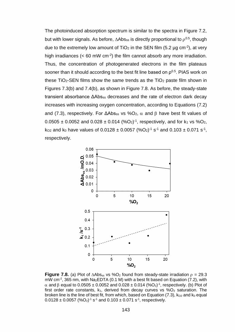
143
The photoinduced absorption spectrum is similar to the spectra in Figure 7.2,
but with lower signals. As before, Absss is directly proportional to 0.5, though
due to the extremely low amount of TiO2 in the SEN film (5.2 µg cm-2), at very
high irradiances (< 60 mW cm-2) the film cannot absorb any more irradiation.
Thus, the concentration of photogenerated electrons in the film plateaus
sooner than it should according to the best fit line based on ρ0.5. PIAS work on
these TiO2-SEN films show the same trends as the TiO2 paste film shown in
Figures 7.3(b) and 7.4(b), as shown in Figure 7.8. As before, the steady-state
transient absorbance ΔAbsss decreases and the rate of electron dark decay
increases with increasing oxygen concentration, according to Equations (7.2)
and (7.3), respectively. For ΔAbsss vs %O2, and have best fit values of
0.0505 ± 0.0052 and 0.028 ± 0.014 (%O2)-1, respectively, and for k1 vs %O2,
kO2 and k0 have values of 0.0128 ± 0.0057 (%O2)-1 s-1 and 0.103 ± 0.071 s-1,
respectively.
Figure 7.8. (a) Plot of Absss vs %O2 found from steady-state irradiation = 29.3 mW cm-2, 365 nm, with Na2EDTA (0.1 M) with a best fit based on Equation (7.2), with
and equal to 0.0505 ± 0.0052 and 0.028 ± 0.014 (%O2)-1, respectively. (b) Plot of first order rate constants, k1, derived from decay curves vs %O2 saturation. The broken line is the line of best fit, from which, based on Equation (7.3), kO2 and k0 equal 0.0128 ± 0.0057 (%O2)-1 s-1 and 0.103 ± 0.071 s-1, respectively.

144
The α constants between TiO2 paste film and TiO2-SEN film are largely
different and correspond to the general difference in magnitude of ΔAbsss,
while the β constants are within the same range (0.0162 ± 0.0007 cf. 0.028 ±
0.014 (%O2)-1), indicating a similar dependence of steady-state concentration
of electrons on oxygen concentrations. The values of kO2 and k0 for a TiO2-
SEN film are significantly larger than in a TiO2 paste film. The difference in
these constants is perhaps due to the difference in film synthesis, notably the
annealing process for the paste films, and the large difference in photocatalyst,
which in theory could provide more deep trapping sites for electrons that are
harder for oxygen to be reduced by. TiO2-SEN films were also tested for
steady-state photoreduction of oxygen like in Figure 7.6, and fitted to Equation
(7.5), where the values of the constants 0.5 and were found to be 0.0108 ±
0.0018 %O2 min-1 and 0.0815 ± 0.0240 (%O2)-1, respectively, as shown in
Figure 7.9.
Figure 7.9. Measured initial rate of the reduction of O2 by 0.1 M Na2EDTA, photocatalysed by a TiO2-SEN film, irradiated with 365 nm LED (10 mW cm-2), as a function of %O2 used to initially saturate the solution. The solid line fit to the data is
based on Equation (7.5) with 0.5 = 0.0108 ± 0.0018 %O2 min-1 and = 0.0815 ± 0.0240 (%O2)-1.
The value of β found with steady-state oxygen photoreduction is again similar
to the value found using PIAS (0.0815 ± 0.0240 cf. 0.028 ± 0.014 (%O2)-1),
and the factor between β values with oxygen reduction and PIAS for both TiO2
paste and TiO2-SEN films were similar (3.4x and 2.9x for paste and SEN film,
respectively), suggesting that the difference in conditions between the two
systems such as reaction volume and stirring consistently affects these
constants.

145
7.4. Conclusion
In conclusion, PIAS, combined with steady-state reaction rate studies, can be
used to probe the reduction of O2 by a SED, photocatalysed by a film
comprised of TiO2 P25 nanoparticles. PIAS has not been used before to
observe transients in P25 paste films, nor have they been observed in films of
monolayer thickness i.e. TiO2-SEN films. To monitor photogenerated electrons
in large timescales of seconds allows for steady-state concentrations to be
found, giving a more accurate picture of how these electrons in a film reduce
nearby electron acceptor species. As mentioned and proven also in Chapter
6, PIAS can be used more widely to provide invaluable mechanistic
information for many different photocatalyst materials, including non-oxides, in
both powder and dense film, and potentially monolayer film forms.
7.5. References
[1] J. Tang, J. R. Durrant and D. R. Klug, J. Am. Chem. Soc., 2008, 130, 13885-91. [2] J. Schneider, K. Nikitin, R. Dillert and D. Bahnemann, Faraday Discuss., 2017, 197, 505-16. [3] L. Xiao-e, A. N. M. Green, S. A. Haque, A. Mills and J. R. Durrant, J. Photochem. Photobiol. A: Chem, 2004, 162, 253-9. [4] H. H. Mohamed, C. B. Mendive, R. Dillert and D. W. Bahnemann, J. Phys. Chem. A, 2011, 115, 2139-47. [5] H. H. Mohamed, R. Dillert and D. W. Bahnemann, J. Photochem. Photobiol. A: Chem, 2011, 217, 271-4. [6] R. Gao, A. Safrany and J. Rabani, Radiat. Phys. Chem., 2003, 67, 25-39. [7] T. Yoshihara, R. Katoh, A. Furube, Y. Tamaki, M. Murai, K. Hara, S. Murata, H. Arakawa and M. Tachiya, J. Phys. Chem. B, 2004, 108, 3817-23. [8] A. M. Peiró, C. Colombo, G. Doyle, J. Nelson, A. Mills and J. R. Durrant, J. Phys. Chem. B, 2006, 110, 23255-63. [9] R. Katoh, M. Murai and A. Furube, Chem. Phys. Lett., 2010, 500, 309-12. [10] S. Ito, P. Chen, P. Comte, M. K. Nazeeruddin, P. Liska, P. Péchy and M. Grätzel, Prog. Photovolt., 2007, 15, 603-12. [11] A. Mills and S. LeHunte, J. Photochem. Photobiol. A: Chem, 1997, 108, 1-35. [12] F. Le Formal, S. R. Pendlebury, M. Cornuz, S. D. Tilley, M. Grätzel and J. R. Durrant, J. Am. Chem. Soc., 2014, 136, 2564-74. [13] C. A. Mesa, A. Kafizas, L. Francàs, S. R. Pendlebury, E. Pastor, Y. Ma, F. Le Formal, M. T. Mayer, M. Grätzel and J. R. Durrant, J. Am. Chem. Soc., 2017, 139, 11537-43. [14] OxySense, https://oxysense.com, accessed April 2021. [15] A. Mills, C. O'Rourke and K. Moore, J. Photochem. Photobiol. A: Chem., 2015, 310, 66-105. [16] C. O'Rourke and A. Mills, Chem. Commun., 2021, 57, 1242-5.

146
Chapter 8
Conclusions & Future Work

147
8.1. Summary
In this work, the first objective was to explore potential avenues into
synthesising novel ultra-thin photocatalytic films, by building upon previous
work by Bell et al. [1, 2]. Primarily, such films made from UV-activated TiO2
and the visible-light absorbing CdS were the aim of this study, as well as
investigating methods of mounting films to improve their robustness and their
workability for potential applications. The second objective of this work was to
examine the kinetics of the photoreduction of oxygen by both monitoring
oxygen consumption and electron decay using Photoinduced Absorption
Spectroscopy (PIAS), in both CdS and TiO2 films. As described in previous
chapters, these aims were met and a summary of each investigated objective
with possible future work for each part of the presented research is given.
8.2. TiO2-SEN films
By combining previous reports of SEN films from silver and gold nanoparticles
[1] with a report of a TiO2 interfacial film that is the prerequisite for making SEN
films [2], a SEN film of TiO2 nanoparticles was created, as reported in Chapter
3. Using commercially sourced TiO2 nanoparticles (Evonik P25), flexible,
optically transparent, and surface-active polystyrene films were formulated.
This was done by creating ion-paired species with protonated TiO2 and an
anionic phase transfer agent, that are consequently most stable in a
water/organic interface to form a monolayer that is subsequently partially
embedded in a polystyrene film formed by evaporation in situ. Following
characterisation, the photoactivity of these films were quantified using various
catalytic tests using 4-chlorophenol, methylene blue and resazurin in solution,
and in inks for the latter two. The TiO2-SEN films were found to be 2-3 times
more active than self-cleaning glass (Pilkington Activ™), which is often used
as a commercial photocatalytic standard.
Due to the versatility of the method to create SEN films, a future avenue to
explore from this work would be to make SEN films from other TiO2
nanoparticles, including other commercial powders, as well as colloids, to
create SEN films with greater photoactivity or with desired properties. The
photocatalytic nature of these films can be utilised to add metal co-catalysts

148
such as gold and platinum onto the nanoparticles through photodeposition.
This allows for the films to be used in photocatalytic reactions that requires a
co-catalyst or would simply improve the efficacy in already possible
photocatalytic reactions. In this work, these films have only been made with
polystyrene, which although produces flexible and transparent films, their
fragile nature means that this is an element that could definitely be improved
upon. Using polymers that are readily flexible even at higher thicknesses e.g.,
poly(methyl methacrylate), polyurethanes and silicones, SEN films of
increased robustness and flexibility would greatly improve their ease of use as
well as versatility in potential applications.
8.3. CdS-SEN films
In Chapter 4, the synthesis of a SEN film with a visible light-absorbing
photocatalyst in the form of cadmium sulfide was reported. The production of
CdS-SEN films further displays the versatility of the method, and again was
the first report of a visible-light photocatalyst film partially embedded into the
surface of an ultra-thin polymer film. This is contrary to previous reports where
CdS particles are embedded entirely throughout films [3], which have much
lower photoactivities per mass of catalyst. Like with TiO2 films, these CdS films
were tested for their photoactivity, while also minimising the photoanodic
corrosion that is a common drawback with using visible-light photocatalysts,
as was demonstrated when attempting to reduce dissolved oxygen in the
absence of a sacrificial electron donor. By using either ascorbic acid or
ethylenediaminetetraacetate to consume photogenerated holes responsible
for corrosion, CdS photoactivity was tested by monitoring the reduction of
dissolved oxygen, as well as methyl orange, crystal violet and methyl viologen
dyes. With the latter dye, the reversibility of its reduction into the methyl
viologen radical allowed it to act as an electron donor for the reduction of water
to generate hydrogen in the presence of platinum nanoparticles. While the
amount of hydrogen produced was low, the amount produced relative to the
amount of catalyst present was very high, meaning that it would be worthwhile
to further examine this reaction with the intent to fully optimise the reaction to
maximise hydrogen production.

149
With the method of synthesising SEN films being presented as highly versatile
and applicable to virtually any charged nanoparticle colloid/dispersion, a clear
progression of this project would be to continue making SEN films of other
photocatalysts such as ZnO, SrTiO3, WO3 and Fe2O3. As well as these, these
films could be made to consist of other nanoparticles that would benefit from
being placed in a film, for example RuO2 which is used extensively in
photoanodes for water splitting and chlorine evolution from brine [4, 5].
Another way to make films of a desired material would be to create films from
silica nanoparticles, which are typically extremely monodisperse, and grow the
desired material on top of the silica, which in theory would produce a much
more even film with tuneable properties. Particles with similar charges, for
example the CdS synthesised in this work and citrate-reduced platinum
nanoparticles could be mixed together to make a hybrid and potentially multi-
functional SEN film, or that with improved photoactivity and/or photostability.
As well as making SEN films, the method has been tweaked to allow the
polymer layer to form while the mixture is still in emulsion form, thus producing
what were coined nano-microparticles (NMPs) [6]. These NMPs retain
properties and activities of nanoparticles while being made into a bulk material,
much like SEN films, but in much higher quantities compared to SEN film
synthesis. These powders can then be used much like colloids with similar
activities to colloids but can then be easily filtered from solution via filtration.
While NMPs with TiO2 have been reported, they have not yet been made with
CdS nanoparticles, thus CdS NMPs could be synthesised and used for
example for optimum hydrogen generation as mentioned previously when
used in conjunction with a platinum colloid, or with photodeposited platinum.
8.4. Mounting films
One of the main downsides of the SEN films is their gossamer nature and low
ease of handling, so to increase the robustness and ease of use of the films,
a number of methods were employed to add a flexible backing layer to the
films. Originally in Chapter 3, SEN films were mounted on double-sided tape
to attach them to cuvette walls, but in Chapter 4, a method to 3D print a layer
of transparent polypropylene was instead devised so that the resulting films

150
could be used more universally without the presence of adhesive materials.
As outlined in Chapter 5, a heat transfer method was also devised by using a
hot iron, similar to t-shirt transfers, to add backing layers made of polymer
sheets e.g. PET, as well as various fabrics, both natural and synthetic. These
heat transfer methods could be applied to make walls of reaction vessels, or
self-cleaning fabrics that could be used for outdoor textiles, e.g. canopies and
flags. The latter application was investigated by testing a SEN film on cotton
for NOx removal in air, where it was found to have an activity comparable to
current commercial products designed with the same application in mind.
As previously mentioned, one way to improve robustness and flexibility would
be to make the SEN films using a more flexible polymer such PMMA or
silicones, though this would likely require tweaking of the current synthesis as
DCM is likely not a suitable solvent for some polymers, as well as looking into
optimum molecular weights for each solvent, as the film will not form properly
if the polymer solution is too viscous or not viscous enough. However, further
advancing the heat-transfer method in Chapter 5 is a more facile route of
adding these monolayer films onto a wide variety of materials, and this method
should be further investigated, and the process optimised to maximise
adhesion to backing layers, while avoiding potential particle embedding
associated with the applied heat and pressure.
8.5. Photoinduced absorption spectroscopy (PIAS)
The photoreduction of oxygen previously studied and reported in Chapter 4
was further probed as steady-state photocatalysis to compare with the decay
of photogenerated electrons by oxygen in CdS and TiO2 films using
photoinduced absorption spectroscopy (PIAS). From this work reported in
Chapters 6 and 7, a variety of constants were calculated to find the
dependence the rate of oxygen reduction and consequently the decay
photogenerated electrons on the amount of dissolved oxygen present. Such
kinetic studies have not been performed on non-oxide semiconductor
photocatalyst films. The same study was performed on SEN films, which
exhibited similar absorption changes to their paste film counterparts, but
unsurprisingly to a much lower magnitude as a result of the lower amount of
semiconductor found in SEN films. The lower signals measured using the

151
PIAS setup means that a greater relative error is observed, but the results are
still significant, as PIAS has rarely been performed on films of monolayer
thicknesses, if at all.
The PIAS setup in this work could be used extensively to further probe
reactions on photocatalytic surfaces and colloids. A natural progression would
be to examine photogenerated holes in TiO2 films, either brought about by
applying a negative potential if possible, or by using a suitable sacrificial
electron donor such as Ag(I) or Fe(III), or a peroxide, persulfate or periodate
species. For photocatalysts that show coloured reduced centres similar to
Ti(III) in TiO2, photogeneration of electrons can be monitored in films of e.g.
WO3 and SrTiO3. For films that do not typically show coloured reduced centres
such as ZnO, the Burstein effect i.e., a blue shift, as was found with CdS films
in this work can be observed in any semiconductor photocatalyst upon ultra-
bandgap irradiation [7]. Examining other reactions that have been studies in
this work, such as dye reductions, using PIAS would also provide a different
mechanistic insight into these reactions by offering a different perspective.
In short, there are many paths that can be pursued continuing on from this
project, and the versatility of the film synthesis method as well as the potential
for film mounting using heat transfer means that there are potentially limitless
applications for such films, depending on the nanoparticles and supporting
layer used. As well as this, PIAS can be used more expansively with the
current setup to give beneficial information on the mechanisms of various
photocatalytic reactions for a wide range of photocatalysts.
8.6. References
[1] Y. Xu, M. P. Konrad, J. L. Trotter, C. P. McCoy, S. E. J. Bell, Small, 2017, 13, 1602163. [2] Y. Xu, M. P. Konrad, W. W. Y. Lee, Z. Ye, S. E. J. Bell, Nano Lett., 2016, 16, 5255-60. [3] N. Kakuta, J. M. White, A. Campion, A. J. Bard, M. A. Fox, S. E. Webber, J. Phys. Chem., 1985, 89, 48-52. [4] S. Licht, B. Wang, S. Mukerji, T. Soga, M. Umeno, H. Tributsch, J. Phys. Chem. B, 2000, 104, 8920-4. [5] R. K. B. Karlsson, A. Cornell, Chem. Rev., 2016, 116, 2982-3028. [6] Z. Ye, C. Li, N. Skillen, Y. Xu, J. McCabe, P. Robertson, S. E. J. Bell, Appl. Mater. Today, 2019, 15, 398-404. [7] P. V. Kamat, N. M. Dimitrijevic, A. J. Nozik, J. Phys. Chem., 1989, 93, 2873-5.

152
Appendix A
Publications & conferences attended

153
Publications
A. McNeill, N. Wells, Y. Xu, X. Li, S. E. J. Bell and A. Mills, J. Photochem.
Photobiol. A: Chem, 2019, 369, 142-9.
A. McNeill and A. Mills, J. Phys. Energy, 2020, 2, 044003.
A. McNeill, R. Han and A. Mills, J. Photochem. Photobiol. A: Chem, 2020,
398, 112576.
A. McNeill, C. O’Rourke and A. Mills, Chem. Commun., 2021, 57, 1591-4.
Conferences attended
2018 Joint UK&Ireland/Spain Semiconductor Photochemistry meeting, 11-
12th September 2018, Gran Canaria, Spain. Oral Presentation:
“Characterisation of clear, transparent TiO2 films from P25”

152

153

154

155

156