Embed Size (px)
Citation preview

DIPLOMARBEIT
Titel der Diplomarbeit
Three-Dimensional Modeling of a
Nanowire Field-Effect Biosensor
(BioFET)
angestrebter akademischer Grad
Magister der Naturwissenschaften (Mag. rer. nat.)
Verfasser: Stefan Andreas BaumgartnerMatrikel-Nummer: A 0502280Studienrichtung: MathematikBetreuer: Dr. Clemens Heitzinger
Wien, Juni 2009


Acknowledgements
First of all I want to thank all the people who supported me in my studies, withmy diploma thesis or in my life and also those who are not mentioned by namein the following.
First I thank my adviser Clemens Heitzinger for giving me the chance to writemy diploma thesis with the support of his FWF (Austrian Science Fund) projectand that he always had time for me to give me advice. I also thank many otherWPI (Wolfgang Pauli Institute) members for taking me in very well and in par-ticular WPI director Norbert Mauser, who helped me with my requests and mymathematical problems, and Alena Bulyha, who worked with me in this projectand with whom I discussed many ideas.
Furthermore I thank my family for giving me the required background and pri-marily my parents Gertrude and Anton Baumgartner who made my studies pos-sible at all.
Finally I thank all my friends for supporting me in my daily life.
Financial support by the OeAW-Stadt Wien project ”Multi-Scale Modeling andSimulation of Field-Effect Nano-Biosensors” and the FWF project ”Mathemati-cal Models and Characterization of BioFETs” is acknowledged, as well as supportby the Wolfgang Pauli Institute.


Abstract
This work deals with the modeling and simulation of a biologically sensitive field-effect transistor, a so called BioFET.
Since the functioning of BioFETs is not completely understood, there is a greatinterest in mathematical and physical models which lead to a quantitative under-standing. In this work, a mathematical model for a nanowire field-effect biosensoris developed to gain insight into its physical behavior.
In the following we will describe the model equations as well as their discretiza-tion. The basic equation of our model is the Poisson equation for the electrostaticinteraction of the charge carriers. Furthermore we use the drift-diffusion equa-tions for the dynamics in the semiconductor and a Boltzmann model for the liq-uid. The interface conditions are resolved with a homogenization method wherethe continuity conditions at the interface are replaced with jump conditions. Thediscretization methods used for this work are the finite-volume method and theScharfetter-Gummel method for the drift-diffusion equations. Finally the nu-merical algorithm and simulation results are shown in detail.
This work is organized as follows:
• Chapter 1 gives an introduction to biosensors and their functionality.Also the advantages of biosensors and the mathematical problems in theirmodeling are described.
• Chapter 2 defines the model used in our simulations, based on the Poissonequation coupled to the drift-diffusion equations. We also use the Poisson-Boltzmann term to include screening in ionic solutions. At the end thevariables and their units are summarized.
• Chapter 3 explains the discretization methods: the finite-volume methodand the Scharfetter-Gummel algorithm.
• Chapter 4 describes the discretization of the model equations. Interfaceconditions are obtained from homogenization.
• Chapter 5 illustrates the modifications of the discretization, which are onthe one hand necessary to get a linear equation system for the potential

vi
and on the other hand necessary for a fast implementation.
• Chapter 6 specifies the numerical algorithm used for the simulations inpseudo-code.
• Chapter 7 varies different simulation parameters and shows the numericalresults for the electric potential, the hole and the electron density, thecurrent flow, and the source-drain current.

Zusammenfassung
Diese Arbeit behandelt einen biologisch sensitiven Feldeffekttransistor, einen so-genannten BioFET.
Weil die Funktionalitat solcher BioFETs noch nicht vollstandig verstanden wurdeherrscht ein großes Interesse an mathematischen und physikalischen Modellen,welche zu einem quantitativen Verstandnis fuhren. In dieser Arbeit wurde einmathematisches Modell erarbeitet um mehr Einsicht in das physikalische Verhal-ten zu bekommen.
Im Folgenden werden wir die Modellgleichungen und die Diskretisierungbeschreiben. Die Gleichung von der wir ausgehen, ist die Poisson Gleichung.Weiters benutzen wir die Drift-Diffusions Gleichungen als Halbleitergleichungenund ein Boltzmann Modell fur die wassrige Losung. Die Stetigkeitsbedingun-gen an der Schnittstelle werden mittels einer Homogenisierungsmethode durchSprungbedingungen ersetzt. Die fur die Diskretisierung benutzten Methodensind die finite Volumen Methode und die Scharfetter-Gummel Methode fur dieDrift-Diffusionsgleichungen. Als Abschluss werden der numerische Algorithmussowie die numerischen Resultate prasentiert.
Diese Arbeit ist auf folgende Weise strukturiert:
• Kapitel 1 gibt eine Einfuhrung in das Thema Biosensoren und deren Funk-tionsweise. Weiters werden die Vorteile von Biosensoren und die mathe-matischen Probleme, die sie verusachen, beschrieben.
• Kapitel 2 definiert das, fur unsere Simulationen verwendete, Modell. Hi-erbei verwenden wir als Grundlage die Poisson Gleichung und fur denHalbleiterteil die Drift-Diffusions-Gleichungen. Wir verwenden auch denPoisson-Boltzmann Term um eine Rasterung in ionischen Losungen zu er-halten. Im Anhang werden die Variablen und ihre Einheiten zusammenge-fasst.
• Kapitel 3 zeigt die verwendeten Methoden zur Diskretisierung. Diese sinddie finite Volumen und die Scharfetter-Gummel Methode.
• Kapitel 4 beschreibt die Diskretisierung der Modellgleichungen. DieSchnittstellenbedingungen werden durch eine Homogenisierungsmethode

viii
bestimmt.
• Kapitel 5 erlautert die benutzten Modifikationen der Diskretisierung, welcheeinerseites notwendig waren, um ein lineares System fur die Gleichungen desPotentials zu bekommen und andererseits notwendig um die Geschwindigkeitdes Programms zu erhohen.
• Kapitel 6 beschreibt den, fur die Simulationen benutzten, Programmal-gorithmus.
• Kapitel 7 benutzt verschiedene Werte fur Simulationen und zeigt die da-raus folgenden numerischen Resultate fur das elektrische Potential, dieLocher- und Elektronendichte, dem Stromfluss und dem Strom zwischenden Kontakten.

Contents
1 Introduction 11
2 The model 132.1 The three-dimensional model of the nanowire biosensor . . . . . . . . 132.2 The model equations . . . . . . . . . . . . . . . . . . . . . . . . . . . 142.3 Variables and units . . . . . . . . . . . . . . . . . . . . . . . . . . . . 18
3 Discretization methods 193.1 The finite-volume method . . . . . . . . . . . . . . . . . . . . . . . . 193.1.1 The general idea of the finite-volume method . . . . . . . . . . . . . 193.1.2 Example . . . . . . . . . . . . . . . . . . . . . . . . . . . . . . . . . 203.2 The Scharfetter-Gummel method . . . . . . . . . . . . . . . . . . . . 22
4 Discretization of the model equations 254.1 The silicon domain . . . . . . . . . . . . . . . . . . . . . . . . . . . . 274.2 The liquid and the oxide domain . . . . . . . . . . . . . . . . . . . . 284.2.1 The liquid domain . . . . . . . . . . . . . . . . . . . . . . . . . . . . 284.2.2 Linearization of the Boltzmann term . . . . . . . . . . . . . . . . . . 284.2.3 The oxide domain and the interface conditions . . . . . . . . . . . . 294.3 The boundary conditions . . . . . . . . . . . . . . . . . . . . . . . . 31
5 Improvements for 3D simulations 335.1 Exploiting the symmetry . . . . . . . . . . . . . . . . . . . . . . . . 335.2 Efficient implementation of the interface conditions . . . . . . . . . . 335.3 Matrix structure . . . . . . . . . . . . . . . . . . . . . . . . . . . . . 37
6 The program 39
7 Simulation and numerical results 417.1 Boundary conditions . . . . . . . . . . . . . . . . . . . . . . . . . . . 427.2 Current flow . . . . . . . . . . . . . . . . . . . . . . . . . . . . . . . 677.3 Influence of Na+Cl− concentration . . . . . . . . . . . . . . . . . . . 707.4 Interface . . . . . . . . . . . . . . . . . . . . . . . . . . . . . . . . . 737.5 Current . . . . . . . . . . . . . . . . . . . . . . . . . . . . . . . . . . 747.6 Conclusion . . . . . . . . . . . . . . . . . . . . . . . . . . . . . . . . 76

x Contents
Bibliography 77

1 Introduction
Since the first biosensor was developed by Clark in 1962, many efforts have beenmade to create functional hybrid systems [9]. Hence many different types ofbiosensors have been created. One of the most attractive approaches is the useof an ISFET (ion-selective field-effect transistor). Bergveld invented the ISFETin 1970 and up to this day the interest in ISFET-based biosensors, so calledbiologically modified field-effect transistors (BioFETs), is enormous. The rangeof applications reaches from biomedicine, biotechnology, food and drug industry,environmental monitoring and process technology to defense and security [10].
These BioFETs belong to the class of electrochemical biosensors, which are sen-sors with an electrochemical transducer. A more precise definition of a BioFETis given by the International Union of Pure and Applied Chemistry (IUPAC):An electrochemical biosensor is a self-contained integrated device, which is capa-ble of providing specific quantitative or semi-quantitative analytical informationusing a biological recognition element (biochemical receptor) which is retainedin direct spatial contact with an electrochemical transduction element [13]. Theidea behind such biosensors is to transform biochemical information into a phys-ical or chemical signal. Therefore the electronic conducting, semiconducting orionic conducting material is coated with a biochemical film. Some examples forsuch biological recognition elements are enzymes, biological ionophores, antibod-ies, plant or animal tissues, whole cells and proteins.
Figure 1.1: Schematic diagram of a nanowire BioFET [2].

12 1 Introduction
Figure 1.1 shows how a BioFET works. The transducer is a semiconductor layerwhich is surrounded by a dielectric layer. In our model it consists of siliconand is surrounded by silicon oxide. Furthermore there is a biofunctionalized sur-face which we call the boundary layer. For example, a DNA sensor uses ssDNA(single-stranded deoxyribonucleic acid) as recognition elements and the comple-mentary strands as target molecules. After hybridization of the DNA strands, thecharge distribution in the boundary layer changes and can be measured throughthe conductance of the semiconductor.
The main advantage of BioFETs is label-free operation, i.e., no fluorescent or ra-dioactive markers are needed. Further advantages are high sensitivity, real-timeoperation and high selectivity [15].
Several facts have to be taken into account for the modeling and simulationof BioFETs. First we have to connect two systems: the biological system, i.e.,the biofunctionalized surface layer, and an electronic system, i.e., the semicon-ductor transducer. Another fact is that we have a multiscale problem. On theone hand, the recognition elements on the functionalized surface are only up toa few nanometers large. On the other hand, the length of the biosensor can bea few micrometers. The problem with these multiple length scales is that theyrequire an extremely fine grid. To solve this problem, we homogenize the bound-ary layer between the oxide and the liquid solution [2].
Our biosensor model is based on experimental structures [4, 11, 12]. Figure1.2 shows such a structure including the source contact, the drain contact, thebackgate at the bottom, and the nanowire.
Figure 1.2: An experimental BioFET structure [11].

2 The model
In this chapter we describe the model equations related to Figure 1.2.
2.1 The three-dimensional model of the nanowirebiosensor
Figure 2.1 shows the cross section through the biosensor which is marked inFigure 1.2 by a yellow line. To simplify the following descriptions, we define the
Figure 2.1: A cross section through the nanowire biosensor.
following domains:
• The silicon-oxide domain:ΩOx := [−xLiq, xLiq]×(0, yOx1)× [O,Lz]∪(−xOx,−xSi)× [yOx1, ySi]× [0, Lz]∪ (xSi, xOx)× [yOx1, ySi]× [0, Lz] ∪ (−xOx, xOx)× (ySi, yOx2)× [0, Lz].

14 2 The model
• The silicon domain:ΩSi := [−xOx, xOx]× [yOx1, ySi]× [0, Lz].
• The liquid domain:ΩLiq := [−xLiq, xLiq]× [yOx2, yLiq]× [0, Lz] ∪ [−xLiq,−xOx]× [yOx1, yOx2]×[0, Lz]∪ [xOx, xLiq]× [yOx1, yOx2]× [0, Lz].
• The whole biosensor Ω := ΩOx ∪ ΩSi ∪ ΩLiq.
• The interface between the liquid area and the oxide area ∆ := ∂ΩOx∩∂ΩLiq.
2.2 The model equations
In this section we give equations for the electric potential V , the concentrationn of the electrons, and the concentration p of the holes. All other values areconstants which are shown in Table 2.1 at the end of this section.The main equation for the electric potential V is the mean-field Poisson equation
−∇ · (ε(x)∇V (x)) = n(x) (2.1)
where x ∈ R3, ε is the permittivity, and n is the charge distribution.The permittivity ε is defined as the piecewise constant function
ε(x) :=
εOx ∈ R for x ∈ ΩOx,
εSi ∈ R for x ∈ ΩSi,
εLiq ∈ R for x ∈ ΩLiq.
(2.2)
For the charge distribution n we have three different models: the doping of thesemiconductor and the electrons and the holes in the domain ΩSi, the ions in theliquid in the domain ΩLiq, and the equation for the dielectric layer in the domainΩOx. Hence we have the partition
n(x) :=
nOx(x) for x ∈ ΩOx,
nSi(x) for x ∈ ΩSi,
nLiq(x) for x ∈ ΩLiq.
(2.3)
For the silicon domain we use the drift-diffusion model [5], which is the set of

2.2 The model equations 15
equations
nSi(x) = C(x) + p(x)− n(x),
∇ · Jn = R,
∇ · Jp = −R,Jn = Dn∇n− µnn∇V,Jp = −Dp∇p− µpp∇V,
(2.4)
where C is the doping concentration, n and p are the concentrations of the freecarriers, namely electrons and holes, Jn and Jp are the densities of the electronand hole currents, Dn and Dp are the diffusion coefficients, and µn and µp arethe mobilities of electrons and holes. The second and the third equation are forthe charge sources given by the recombination rate R, which is in our model theShockley-Read-Hall term
R =np− n2
i
τp(n+ ni) + τn(p+ ni), (2.5)
where τn and τp are the lifetimes of electrons and holes and ni is the intrinsiccharge density of the semiconductor material. Furthermore we use the Einsteinrelations
Dn = UTµn,
Dp = UTµp,(2.6)
for the diffusion coefficients where UT is the thermal voltage and has a value of≈ 0.025V for silicon at room temperature.In the oxide we set only nOx(x) := 0 and in the liquid we have
nLiq(x) :=∑
σ∈−1,1
ασfσe−σβV (x), (2.7)
which is a Boltzmann model. This Boltzmann model describes the screening inionic solutions. Here fσ stands for the exponential of the chemical potentialsΦσ, i.e., fσ = eσβΦσ and β := q/(kT ), where q is the elementary charge, k is theBoltzmann constant, and T is the temperature. Furthermore α is the Na+Cl−
concentration in the liquid.At the interface ∆ we replace the continuity condition for the potential and thecontinuity condition for the electric displacement using a homogenization method

16 2 The model
[2] by the following jump conditions
V (x+)− V (x−) =D
ε(x+), (2.8)
εLiq∇V (x+)− εOx∇V (x−) = −Cs (2.9)
where x+ denotes the limes from the liquid to the interface and x− denotes thelimes from the silicon oxide to the interface (see Figure 2.2).
Figure 2.2: Vectors pointing to the interface.
Here D is the macroscopic dipole moment density and Cs is the macroscopicsurface charge density which are shown in [2]. Here we treat them as given con-stants.The boundary ∂Ω of the biosensor has Dirichlet conditions at the backgate, atthe electrode, and at the source and drain contacts, and Neumann boundaryconditions everywhere else. The source and the drain contacts are Ohmic con-tacts, hence the space charge vanishes, i.e., C + p− n = 0, and the system is inthermal equilibrium, i.e., np = n2
i . The quasi Fermi levels Φn and Φp are definedby
Φn := V − UT ln
(n
ni
),
Φp := V + UT ln
(p
ni
) (2.10)

2.2 The model equations 17
and the values of the applied voltage U at Ohmic contacts are assumed as Φn =U = Φp. Hence we get the boundary conditions
n(x) =1
2(C +
√C2 + 4n2
i ),
p(x) =1
2(−C +
√C2 + 4n2
i ),
V (x) = U + UT log
(n(x)
ni
)= U − UT ln
(p(x)
ni
) (2.11)
at the Ohmic contacts.
Figure 2.3: Boundary conditions at the electrode and at the backgate and theoutward pointing normal vector t.
The Neumann conditions
∇V (x) · t = 0 (2.12)
are used everywhere else, where t is the outward pointing normal vector. At lastwe have the Dirichlet conditions
V (x) = Vb,
V (x) = Ve(2.13)
at the boundaries of the backgate and the electrode.

18 2 The model
2.3 Variables and units
The following table shows the variables and their units used in this model.
Meaning Variable Unit or value
Temperature T KElementary charge q q = 1.60218 · 10−19CBoltzmann constant k 8.31452 · 10−3kJ ·mol−1 ·K−1
Electric potential V, U,Φ kJ ·mol−1 · q−1 = 0.010364272VCharge density n, p q · nm−3
Macroscopic surface charge density Cs q · nm−2
Macroscopic dipole moment density D q · nm−1
Electron lifetime τn 106ps (silicon)Hole lifetime τp 107ps (silicon)Electron low-field mobility µn 1.5 · 105nm2 · V−1 · ps−1 (silicon)Hole low-field mobility µp 4.5 · 104nm2 · V−1 · ps−1 (silicon)Diffusion coefficient Dn, Dp nm2 · ps−1
Current flow J q · nm2 · ps−1
Recombination rate R q · nm2 · ps−1
Permittivity of silicon εSi 11.9ε0
Permittivity of silicon oxide εOx 3.9ε0
Permittivity of water εLiq 80.1ε0
Thermal voltage UT 0.025VDoping concentration C q · nm−3
Table 2.1: The variables and their units.

3 Discretization methods
3.1 The finite-volume method
In this section we follow the explanations of [3]. The finite-volume method is adiscretization method that is especially advantageous for numerical investigationsof partial differential equations in divergence form
∂tS(u) +∇ · (M(u)−K(∇u)) = Q(u), (3.1)
where S is a storage term, M is a convective part, K is a diffusive part, and Q isa source term. S,M,K, and Q can depend linearly or nonlinearly on u. It is alsouseful for partial differential equations where parts are in divergence form, forinstance parabolic partial differential equations. In the category of second-orderlinear elliptic partial differential equations the form
Lu := −∇ · (K∇u− cu) + ru = f (3.2)
with K : Ω→ Rd,d, c : Ω→ Rd and r, f : Ω→ R is common. Also the parabolicversion
∂u
∂t+ Lu = f, (3.3)
partial differential equations of first order
∇ · q(u) = 0 (3.4)
with nonlinear q : R → Rd, partial differential equations of higher order andsystems of partial differential equations can be solved numerically with the finite-volume method.
3.1.1 The general idea of the finite-volume method
To deliver insight into the finite-volume method we consider the equation
∇ · q(u) = f. (3.5)

20 3 Discretization methods
The first step of the finite-volume method is to partition the simulation domainΩ. The sub-domains Ωi have to fulfill the following properties:
• each Ωi is open, simply connected, and has a polygonal border,
• Ωi ∩ Ωj = 0/ for (i 6= j),
•⋃Mi=1 Ωi = Ω.
The sub-domains are called control volumes or control areas. The next step isto integrate (3.5) over the control volume Ωi and use the divergence theoremyielding ∫
∂Ωi
ν · q(u)dσ =
∫Ωi
fdx, i ∈ 1, ...,M, (3.6)
where ν is the outward pointing normal vector on ∂Ωi. Because of our require-ments, the border ∂Ωi consists of ni lines. So we can write (3.6) as
ni∑j=1
∫Γij
νij · q(u)dσ =
∫Ωi
fdx. (3.7)
The last step is to discretize the integrals in (3.7). This can be done in variousways.
3.1.2 Example
For our purposes we consider the linear elliptic PDE with homogeneous boundarycondition in Ω ∈ R2
−∇ · (k∇u− cu) + ru = f for x ∈ Ω,
u = 0 for x ∈ ∂Ω(3.8)
with k, r, f : Ω → R and c : Ω → R2. For our application we need a two-dimensional grid, but also a Delaunay triangulation or other triangulations arealso possible. Integrating both sides yields
−∫
Ωi
∇ · (k∇u− cu)dx+
∫Ωi
rudx =
∫Ωi
fdx ∀i ∈ Λ, (3.9)
where Ωi is a control volume and Λ is the set of points of our two-dimensionalgrid. Now we use the divergence theorem and for the first integral we get
−∫
Ωi
∇ · (k∇u− cu)dx = −∑j∈Λi
∫Γij
νij · (k∇u− cu)dσ, (3.10)

3.1 The finite-volume method 21
where Λi are the neighboring points of the node i and νij is the outward pointingnormal of Γij. In the next step we approximate k and νij · c on Γij by constantsµij and γij so that the integral becomes
−∫
Ωi
∇ · (k∇u− cu)dx ≈ −∑j∈Λi
∫Γij
µij(νij · ∇u)− γijudσ. (3.11)
We approximate the normal derivatives by differential quotients, i.e.,
νij · ∇u ≈u(aj)− u(ai)
dijwith dij := |ai − aj|. (3.12)
For the approximation of the integral of u we use the linear interpolation
u|Γij ≈ riju(ai) + (1− rij)u(aj) (3.13)
with rij ∈ [0, 1]. The other two integrals are approximated by∫Ωi
rudx ≈ r(ai)u(ai)mi =: riu(ai)mi∫Ωi
fdx ≈ f(ai)mi =: fimi
(3.14)
with mi := |Ωi|. In summary we have the system of equations∑j∈Λi
(µij
ui − ujdij
+ γij (rijui + (1− rij)uij))mij + riuimi = fimi, i ∈ Λ.
(3.15)

22 3 Discretization methods
3.2 The Scharfetter-Gummel method
We use the Scharfetter-Gummel discretization [8] for the drift-diffusion equations
∇ · Jn = R,
∇ · Jp = −R,Jn = Dn∇n− µnn∇V,Jp = −Dp∇p− µpp∇V.
(3.16)
To discretize the first two equations we use the finite-volume method. Hence wehave
m1(Jni+ 1
2,j,k− Jn
i− 12,j,k
) +m2(Jni,j+ 1
2,k− Jn
i,j− 12,k
)
+m3(Jni,j,k+ 1
2− Jn
i,j,k− 12) = R(i, j, k) ·m,
m1(Jpi+ 1
2,j,k− Jp
i− 12,j,k
) +m2(Jpi,j+ 1
2,k− Jp
i,j− 12,k
)
+m3(Jpi,j,k+ 1
2
− Jpi,j,k− 1
2
) = −R(i, j, k) ·m,
(3.17)
where m1, m2, and m3 are the areas of the boundary surfaces of the control vol-ume and m is the volume of the whole control volume. To simplify the followingexplanations, we rewrite the third and fourth equation in the form
J = −(a∇u+ bu), (3.18)
where a = −Dn and a = Dp, respectively, u = n and u = p, respectively, andb = µn∇V and b = µp∇V , respectively. Now we set ψ := b
aand have
J = −(a∇u+ bu)
= −a∇ueψe−ψ − au1
abeψe−ψ
= −ae−ψ(eψ∂u+ u∂eψ)
= −ae−ψ∂(eψu).
(3.19)
In the next step we use the assumption that J is constant on every surface of ourcontrol volume. Then we have to integrate over the edges of our discretization.To illustrate the method we take the edge between xi and xi+1 and get
−a−1J
∫ xi+1
xi
eψdx =
∫ xi+1
xi
∂(eψu) = δ(eψu). (3.20)

3.2 The Scharfetter-Gummel method 23
The other edges are analogeous. For the last computation we use linear interpo-lation for ψ and have ∫ xi+1
xi
eψdx =eψ
ψ
∣∣∣∣xi+1
xi
· (xi+1 − xi), (3.21)
so that we have, for ψ = − µnDnV and ψ = − µp
DpV , respectively, the formulas
Jni+ 1
2,j,k
= −µn(Vi+1,j,k − Vi,j,k)(ecnVi+1,j,kni+1,j,k − ecnVi,j,kni,j,k)(ecnVi+1,j,k − ecnVi,j,k)(xi+1 − xi)
,
Jpi+ 1
2,j,k
= −µp(Vi+1,j,k − Vi,j,k)(ecpVi+1,j,kpi+1,j,k − ecpVi,j,kpi,j,k)(ecpVi+1,j,k − ecpVi,j,k)(xi+1 − xi)
,
(3.22)
where cn := − µnDn
and cp := µpDp
. The formulas for the discretization of the flows
in y and in z directions are analogeous. Finally we substitute (3.22) into (3.17)to get the entire discretization.
In the next chapter we will use this method to discretize the model equations.


4 Discretization of the modelequations
For the discretization of the model equations we use a 3-dimensional mesh whichis equidistant in each coordinate direction. Therefore we use the same axes asin Figure 2.1. We call the distance between two points dx, dy, and dz. Further-more we call the value of the potential V at the mesh point (i, j, k) Vi,j,k andsimilarly the density of the holes ni,j,k, the density of the electrons pi,j,k, and therelated current flows, Jn
i+ 12,j,k
and Jpi+ 1
2,j,k
, Jni,j+ 1
2,k
and Jpi,j+ 1
2,k
, and Jni,j,k+ 1
2
and
Jpi,j,k+ 1
2
, respectively. To discretize the whole biosensor we consider each domain
separately. The left-hand side of the Poisson equation (2.1) is the same for eachdomain, and therefore we use the finite-volume method. We have to define acontrol volume Ωi,j,k for every mesh point (i, j, k).
Figure 4.1: Five control volumes with grid points at the centers of the boxes.

26 4 Discretization of the model equations
Here we use the control volumes
Ωi,j,k := x := (x1, x2, x3) ∈ Ω : |x1 − i · dx| ≤dx
2and |x2 − j · dy| ≤
dy
2
and |x3 − k · dz| ≤dz
2
.
(4.1)
As the next step in the finite-volume method we integrate the Poisson equationover the control volumes and use the divergence theorem to get
−∫
Ωi,j,k
∇ · (ε(x)∇V (x)) dx = −∑
l∈Λi,j,k
∫Γl
νlε(x)∇V (x)dσ, (4.2)
where Λi,j,k is the set of the neighbor points of the node (i, j, k), Γl is the bound-ary of the control volume on which the point l is provided and νl is the outwardspointing normal on Γl (see Figure 4.2).
Figure 4.2: A control volume with 3 outward pointing normal vectors.
Now we consider a single neighboring point l and approximate the normal deriva-tive by the differential quotient
νl · ∇V ≈Vl1,l2,l3 − Vi,j,k
d, (4.3)
where d is dx, dy or dz depending on the direction where the normal vectorνl points. To complete the discretization of the left-hand side of the Poissonequation we use our assumption that the permittivity ε is a piecewise constant

4.1 The silicon domain 27
function and get∑j∈Λi
∫Γij
νijε(x)∇V (x)dσ =
−(εi+ 1
2,j
Vi+1,j,k − Vi,j,kxi+1 − xi
− εi− 12,j
Vi,j,k − Vi−1,j,k
xi − xi−1
)· dy · dz
−(εi,j+ 1
2
Vi,j+1,k − Vi,j,kyj+1 − yj
− εi,j− 12
Vi,j,k − Vi,j−1,k
yj − yj−1
)· dx · dz
−(εi,j
Vi,j,k+1 − Vi,j,kzk+1 − zk
− εi,jVi,j,k − Vi,j,k−1
zk − zk−1
)· dx · dy.
(4.4)
As mentioned before, we now have to consider the different models for the do-mains to arrive at the discretizations of the right-hand side of equation (2.1).We discuss the discretization in the silicon domain ΩSi first.
4.1 The silicon domain
In the silicon domain ΩSi we have to solve the drift-diffusion equations (2.4).To discretize the electron and hole densities, we use the Scharfetter-Gummeldiscretization. Hence we have
m1
(µ(Vi,j,k − Vi−1,j,k(e
cVi,j,kui,j,k − ecVi−1,j,kui−1,j,k)
(ecVi,j,k − ecVi−1,j,k)dx
−µ(Vi+1,j,k − Vi,j,k(ecVi+1,j,kui+1,j,k − ecVi,j,kui,j,k)(ecVi+1,j,k − ecVi,j,k)dx
)+m2
(µ(Vi,j,k − Vi,j−1,k(e
cVi,j,kui,j,k − ecVi,j−1,kui,j−1,k)
(ecVi,j,k − ecVi,j−1,k)dy
−µ(Vi,j+1,k − Vi,j,k(ecVi,j+1,kui,j+1,k − ecVi,j,kui,j,k)(ecVi,j+1,k − ecVi,j,k)dy
)+m3
(µ(Vi,j,k − Vi,j,k−1(ecVi,j,kui,j,k − ecVi,j,k−1ui,j,k−1)
(ecVi,j,k − ecVi,j,k−1)dz
−µ(Vi,j,k+1 − Vi,j,k(ecVi,j,k+1ui,j,k+1 − ecVi,j,kui,j,k)(ecVi,j,k+1 − ecVi,j,k)dz
)=σRi,j,k ·m,
(4.5)
where u stands for n or p and σ = +1 for u = n and σ = −1 for u = p. Similarlyc stands for cn or cp and µ for µn or µp, which are the values from Chapter 3.For the recombination rate we use the Shockley-Read-Hall term with the values

28 4 Discretization of the model equations
of n and p at the mesh points
Ri,j,k =ni,j,kpi,j,k − n2
i
τp(ni,j,k + ni) + τn(pi,j,k + ni). (4.6)
Finally we use the finite-volume method for the right-hand side of the Poissonequation. Therefore we integrate the right side over the control volume Ωi,j,k
which was used at the left-hand side and approximate C, n and p to have∫Ωi,j,k
C + n(x)− p(x)dx = (C + ni,j,k − pi,j,k) ·m, (4.7)
where ni,j,k and pi,j,k are given by the Scharfetter-Gummel discretization, C isthe doping concentration and m is again the volume of the control volume Ωi,j,k.
4.2 The liquid and the oxide domain
We discuss the other two domains, the liquid and the oxide, together, because wehave to obtain the discretization of the interface conditions where both domainsare involved.
4.2.1 The liquid domain
To discretize the right-hand side of the Poisson equation for the liquid we coulduse ∫
Ωi
∑σ∈−1,1
ασfσe−σβV (x)dx =
∑σ∈−1,1
ασfσe−σβVi,j,k ·m. (4.8)
There are two problems, however. First the homogenization method works onlyfor linear operators. Second, this yields a system of nonlinear equations, whereasthe following linearization allows us to simplify the problem to a system of linearequations.
4.2.2 Linearization of the Boltzmann term
To linearize the Boltzmann term around V0 we rewrite it as∑σ∈−1,1
ασe−σβ(V−Φ) =∑
σ∈−1,1
ασe−σβ(V−V0)e−σβ(V0−Φ)
(4.9)

4.2 The liquid and the oxide domain 29
and replace e−σβ(V−V0) by the Taylor series. Hence we get∑σ∈−1,1
ασe−σβ(V−V0)e−σβ(V0−Φ) =∑
σ∈−1,1
ασe−σβ(V0−Φ)(1− σβ(V − V0) +O(V 2))
= 2(−α sinh β(V0 − Φ) + αβV0 cosh β(V0 − Φ)− αβV cosh β(V0 − Φ)).
(4.10)
For the linearization around V0 = 0 we have∑σ∈−1,1
ασe−σβ(V−Φ) ≈ 2α(sinh βΦ− βV cosh βΦ) (4.11)
as the Boltzmann term in the discretization.
4.2.3 The oxide domain and the interface conditions
In the oxide, the right-hand side is equal to zero and so we have only to obtainthe discretization for the jump conditions
V (x+)− V (x−) =D
εLiq, (4.12)
εLiq∇V (x+)− εOx∇V (x−) = −Cs (4.13)
at the interface ∆.
Figure 4.3: The parts of the interface.
Therefore we divide the interface into 4 parts (see Figure 4.3): the horizontal

30 4 Discretization of the model equations
interface ∆1, the vertical interface ∆2, the interface vertices ∆3 on the right sideof the nanowire, and the interface vertices ∆4 on the left side of the nanowire.We denote the left- and right-hand side limits by substracting and adding 1
4in
the index. This yields
Vi,j+ 14,k − Vi,j− 1
4,k =
D
εLiq,
εLiqVi,j+1,k − Vi,j+ 1
4,k
dy− εOx
Vi,j− 14,k − Vi,j−1,k
dy= −Cs,
(4.14)
at the interface ∆1,
Vi− 14,j,k − Vi+ 1
4,j,k =
D
εLiq,
εLiqVi−1,j,k − Vi− 1
4,j,k
dx− εOx
Vi+ 14,j,k − Vi+1,j,k
dx= −Cs,
(4.15)
at the left side of the interface ∆2,
Vi+ 14,j,k − Vi− 1
4,j,k =
D
εLiq,
εLiqVi+1,j,k − Vi+ 1
4,j,k
dx− εOx
Vi− 14,j,k − Vi−1,j,k
dx= −Cs,
(4.16)
at the right side of the interface ∆2,
Vi+ 14,j+ 1
4,k − Vi− 1
4,j− 1
4,k =
D
εLiq,
εLiq2(Vi+1,j+1,k − Vi+ 1
4,j+ 1
4,k)√
dx2 + dy2− εOx
2(Vi− 14,j− 1
4,k − Vi−1,j−1,k)√
dx2 + dy2= −Cs,
(4.17)
at the interface ∆3 and
Vi− 14,j+ 1
4,k − Vi+ 1
4,j− 1
4,k =
D
εLiq,
εLiq2(Vi−1,j+1,k − Vi− 1
4,j+ 1
4,k)√
dx2 + dy2− εOx
2(Vi+ 14,j− 1
4,k − Vi+1,j−1,k)√
dx2 + dy2= −Cs,
(4.18)
at the interface ∆4. Now we have the discretization for the inner points of thesimulation domain and only the boundary conditions are left to complete thediscretization.

4.3 The boundary conditions 31
4.3 The boundary conditions
As mentioned in Chapter 1, we have Dirichlet boundary conditions at the source,drain, and back-gate contacts and at the electrode and Neumann boundary con-ditions everywhere else. The Dirichlet conditions at the electrode and at theback-gate are
Vi,0,k = Vb,
Vi,yLiq,k = Ve(4.19)
for every i and k in our mesh, where Vb and Ve are the same constants as inChapter 1. The boundary conditions at the source and the drain contacts are
Vi,j,0 = Vs + UT lnnDi,j,0ni
,
Vi,j,zL = Vd + UT lnnDi,j,zLni
,
ni,j,0 = nDi,j,0,
ni,j,zL = nDi,j,zL,
pi,j,0 = pDi,j,0,
pi,j,zL = pDi,j,zL
(4.20)
for every i and j in our mesh where
nDi,j,k =1
2(Ci,j,k +
√C2i,j,k + 4n2
i )
and
pDi,j,k =1
2(−Ci,j,k +
√C2i,j,k + 4n2
i )
are the values of the electron and hole densities at the boundary. The Neumannconditions are
VxLiq,j,k = VxLiq−1,j,k,
V−xLiq,j,k = V−xLiq+1,j,k,
Vi,j,1 = Vi,j,2,
Vi,j,zL = Vi,j,zL−1
(4.21)

32 4 Discretization of the model equations
for every i, j and k in our mesh and in the silicon domain we have Neumannconditions for the current flow, which are
Jui,ySi+ 1
2,k
= 0,
Jui,yOx1− 1
2,k
= 0,
JuxSi+ 1
2,j,k
= 0,
Ju−xSi− 12,j,k
= 0
(4.22)
for every k in the mesh, i ∈ [−xSi, xSi] and j ∈ [yOx1, ySi], where u = n or u = p.

5 Improvements for 3Dsimulations
We developed two improvements for the discretization in Chapter 3. The firstchange is that we halve the number of grid points by using the symmetry of thebiosensor. The second improvement is needed because we have to implement theinterface conditions efficiently on an equidistant grid.
5.1 Exploiting the symmetry
A quick look on Figure 1.1 is enough to understand the symmetry of the biosensorand the idea is obvious that we reflect the biosensor about the y-axis. Theadvantage of this reflection is that we only need a bit more than half of thepoints and so the computation is much faster. To get the right conditions forthe points on the y-axis we only have to set
V−1,j,k := V1,j,k
n−1,j,k := n1,j,k
p−1,j,k := p1,j,k
(5.1)
for every index j and k on the grid. As a consequence we can limit the followingexplanations to points with x ≥ 0.
5.2 Efficient implementation of the interfaceconditions
In Chapter 3 we started with an equidistant grid, but we need additional gridpoints for the interface conditions. For instance at the interface ∆1, we callthe two limits Vi,j+ 1
4,k and Vi,j− 1
4,k. The idea is now to use the points Vi,j,k and
Vi,j−1,k instead of the points Vi,j+ 14,k and Vi,j− 1
4,k. This can be done similarly for

34 5 Improvements for 3D simulations
the points at the interface ∆2. So we have the equations
Vi,j,k − Vi,j−1,k =D
εLiq,
εLiqVi,j+1,k − Vi,j,k
dy− εOx
Vi,j−1,k − Vi,j−2,k
dy= −Cs
(5.2)
at the interface ∆1 and
Vi,j,k − Vi−1,j,k =D
εLiq,
εLiqVi+1,j,k − Vi,j,k
dx− εOx
Vi−1,j,k − Vi−2,j,k
dx= −Cs,
(5.3)
at the interface ∆2.
Figure 5.1: Linking of the grid points at the interface. The red points are addi-tional points which are treated in Figure 5.2.
At the interface ∆3 we have the equations
Vi,j,k − Vi−1,j−1,k =D
εLiq,
εLiq2(Vi+1,j+1,k − Vi,j,k)√
dx2 + dy2− εOx
2(Vi−1,j−1,k − Vi−2,j−2,k)√dx2 + dy2
= −Cs.(5.4)
But now we have the problem that we have additional points at (xOx − 1, j, k)where (j, k) ∈ [yOx2, yLiq−1]×[1, Lz−1], (i, yOx2−1, k) where (i, k) ∈ [xOx, xLiq−1]× [1, Lz − 1], (i, yOx1, k) where (i, k) ∈ [0, xOx − 1]× [1, Lz − 1], and (xOx, j, k)where (j, k) ∈ [1, yOx1 − 1] × [1, Lz − 1] which are shown in Figure 5.2 as redpoints. These points does not exist in our original discretization, so we combine

5.2 Efficient implementation of the interface conditions 35
these points with points nearby. First we identify them with existing points byadding the equations
VxOx−1,j,k = VxOx,j,k for (j, k) ∈ ([1, yOx1 − 1] ∪ [yOx2, yLiq − 1])× [1, Lz − 1],
Vi,yOx2,k = Vi,yOx2−1,k for (i, k) ∈ [xOx, xLiq − 1]× [1, Lz − 1],
Vi,yOx1,k = Vi,yOx1−1,k for (i, k) ∈ [0, xOx − 1]× [1, Lz − 1]
(5.5)
and then we have to connect the points in the original grid via the Poissonequation
−(εi+ 1
2,j
Vi+1,j,k − Vi,j,kdx
− εi− 32,j
Vi,j,k − Vi−2,j,k
dx
)· dy · dz
−(εi,j+ 1
2
Vi,j+1,k − Vi,j,kdy
− εi,j− 12
Vi,j,k − Vi,j−1,k
dy
)· dx · dz
−(εi,j
Vi,j,k+1 − Vi,j,kdz
− εi,jVi,j,k − Vi,j,k−1
dz
)· dx · dy = rhs
(5.6)
Figure 5.2: The red points are additional points which identified with blackpoints. The other arrows show the points which are affected by thePoisson equation.
at the points i = xOx and (j, k) ∈ [yOx2+1, yLiq−1]×[1, zL−1], via the equations

36 5 Improvements for 3D simulations
−(εi+ 3
2,j
Vi+2,j,k − Vi,j,kdx
− εi− 12,j
Vi,j,k − Vi−1,j,k
dx
)· dy · dz
−(εi,j+ 1
2
Vi,j+1,k − Vi,j,kdy
− εi,j− 12
Vi,j,k − Vi,j−1,k
dy
)· dx · dz
−(εi,j
Vi,j,k+1 − Vi,j,kdz
− εi,jVi,j,k − Vi,j,k−1
dz
)· dx · dy = rhs
(5.7)
at the points i = xOx and (j, k) ∈ [1, yOx1 − 2]× [1, zL− 1], via the equations
−(εi+ 1
2,j
Vi+1,j,k − Vi,j,kdx
− εi− 12,j
Vi,j,k − Vi−1,j,k
dx
)· dy · dz
−(εi,j+ 1
2
Vi,j+1,k − Vi,j,kdy
− εi,j− 32
Vi,j,k − Vi,j−2,k
dy
)· dx · dz
−(εi,j
Vi,j,k+1 − Vi,j,kdz
− εi,jVi,j,k − Vi,j,k−1
dz
)· dx · dy = rhs
(5.8)
at the points j = yOx2 and (i, k) ∈ [xOx + 1, xLiq− 1]× [1, zL− 1], and finally viathe equations
−(εi+ 1
2,j
Vi+1,j,k − Vi,j,kdx
− εi− 12,j
Vi,j,k − Vi−1,j,k
dx
)· dy · dz
−(εi,j+ 3
2
Vi,j+2,k − Vi,j,kdy
− εi,j− 12
Vi,j,k − Vi,j−1,k
dy
)· dx · dz
−(εi,j
Vi,j,k+1 − Vi,j,kdz
− εi,jVi,j,k − Vi,j,k−1
dz
)· dx · dy = rhs
(5.9)
at the points j = yOx1− 1 and (i, k) ∈ [0, xOx− 2]× [1, zL− 1]. Here rhs standsfor the right-hand side of the respective Poisson equation.

5.3 Matrix structure 37
5.3 Matrix structure
After these improvements the linear system has the structure shown in Figure5.3, which is similar to the usual band structure of discretizations of the Poissonequation.
Figure 5.3: Structure of the linear system.
It also shows that there are non-zero points which are not in the usual bandstructure. These points are the equations for the vertical interface ∆2. Becauseof the small parameters used in the simulation shown in Figure 5.3, not all ofthe 7 bands of the discretization of the 3D Poisson equation are seen.
Figure 5.4: Structure of the linear system with larger parameters.

38 5 Improvements for 3D simulations
In Figure 5.4 larger parameters are used and the 7-band structure is clearly seen.It is also observed in Figure 5.4 that the band structure of the equations withthe interface conditions is not worse than the band structure of the discretizationof the 3D Poisson equation. This means that our implementation works veryefficiently.

6 The program
Listing 6.1 shows the Mathematica program in pseudo code where we use astepping method for the boundary conditions to improve convergence. In Listing6.1 we use as example the boundary conditions at the back-gate and the source.
Listing 6.1: Numerical algorithm.
1 for(i=0,i<iterB , i++)2 Vb=startB+i∗stepB3 for(j=0,j<iterS , j++)4 Vs=startS+j∗stepS5 if(i==0 && j==0) n [0 ]=p [0 ]=0 6 else ifi>0 && j==0)7 n [0 ]= soln [ i−1,j ]8 p [0 ]= solp [ i−1,j ]9
10 else11 n [0 ]= soln [ i , j−1]12 p [0 ]= solp [ i , j−1]13 14
15 k = V [ 0 ] = 016
17 while(k<maxIterations)18 V [ k+1] = B(n [ k ] , p [ k ] )19 n [ k+1] = N(V [ k+1] ,n [ k ] , p [ k ] )20 p [ k+1] = N(V [ k+1] ,n [ k+1] ,p [ k+1])21 deltaV = | | V [ k+1] − V [ k ] | |22
23 if(deltaV < maxDelta) : break24 k++25 26 soln [ i , j ] = n [ k ]27 solp [ i , j ] = p [ k ]28 solV [ i , j ] = V [ k ]29 30

40 6 The program
Here we compute n and p with the Newton method and V with the Bi-CGSTABmethod which is a Krylov method. For more details to the Newton method andthe Bi-CGSTAB method see [1, 7, 14].This schematic program will start with the boundary conditions Vb = startB andVs = startS and will make iterB steps with step size stepB for the back-gateand iterS steps with step size stepS for the source contact. The setting of thestart values of n and p provides a better approximation in the loop where k = 0.Furthermore we use the infinity norm for the computation of deltaV and thetolerance limit maxDelta := 10−6V.

7 Simulation and numericalresults
For the simulations shown in this chapter we consider a leading example. Theparameters of the reference structure are shown in Table 7.1.
dx = 1 dy = 1 dz = 1
xSi = 9nm yOx1 = 9nm Lz = 19nm
xOx = 12nm ySi = 17nm
xLiq = 24nm yOx2 = 20nm
yLiq = 34nm
Table 7.1: The length scales of the example.
If not noted otherwise, the values of Table 7.2 will be used.
Φ = 0 Cs = −2 · 10−19q · nm−2 α = 6.02214 · 10−5mole · nm−3
C = 10−5q · nm−3 D = 0q · nm−2
Table 7.2: Basic setting.
In the following we will often compute the current ISD between source and drain.It is computed by the formula
ISD =
xSi∑i=−xSi
ySi∑j=yOx1+1
(Jpi,j,k− 1
2
+ Jni,j,k− 1
2
), (7.1)
where k is an integer in [2, Lz − 1].

42 7 Simulation and numerical results
7.1 Boundary conditions
In this paragraph we discuss the hole density p, the electron density n, and theelectric potential V for varying boundary conditions. Therefore we use differentcross sections in the plots. The cross sections in x and y-directions are shown inFigure 7.1.
Figure 7.1: Cross sections shown in simulations.
Furthermore the current ISD for varying boundary conditions is summarized inTable 7.3. We chose the parameters in Table 7.3 to investigate the influence ofthe different boundary conditions separately and some of their interactions.
Settings ISD [A]
Vb = 0V, Ve = 0V, Vs = 0V, Vd = 0VVb = −3V, Ve = 0V, Vs = 0V, Vd = 0VVb = 0V, Ve = −1V, Vs = 0V, Vd = 0VVb = 0V, Ve = 0V, Vs = 5V, Vd = 0VVb = 0V, Ve = 0V, Vs = 0V, Vd = 5VVb = 0V, Ve = 0V, Vs = −5V, Vd = 5VVb = −2V, Ve = 1V, Vs = 0V, Vd = 0VVb = −2.5V, Ve = 2.5V, Vs = −5V, Vd = 5V
5.93208 · 10−23
9.85995 · 10−28
−1.12338 · 10−26
1.43795 · 10−6
−1.43795 · 10−6
−33.3354 · 10−6
4.13576 · 10−22
−40.3515 · 10−6
Table 7.3: Current for varying boundary conditions.

7.1 Boundary conditions 43
Results for Vb = 0V, Ve = 0V, Vs = 0V, Vd = 0V
Figure 7.2 shows the electric potential in cross sections in x-direction. The threecross sections at the top (always from left to right) are for the values x = 0nm,x = 10nm, and x = 12nm and the three cross sections at the bottom are for thevalues x = 14nm, x = 19nm, and x = 23nm. The common of all six picturesare that we see the boundary condition for the back-gate at the left side of thepictures and the boundary condition for the electrode at the right side of thepictures. In the three figures at the top we see how the semiconductor (fromy = 9nm to y = 17nm) influences the electric potential V and that the boundaryconditions at the source and the drain for the Ohmic contacts depend not onlyon the applied voltage, see (2.11). The three pictures at the bottom show theresults at the surface with zero-flux boundary conditions at the left- and on theright-hand side (at x = −24nm and x = 24nm) of the biosensor in contrast toDirichlet boundary conditions.
Figure 7.2: Cross sections at x = 0nm, x = 10nm, x = 12nm, x = 14nm, x = 19nm, and x = 23nm showing the electric potential V .
The cross sections at z = 5nm, z = 10nm, and z = 15nm are shown in Figure 7.3where the semiconductor part from x = −9nm to x = 9nm and from y = 9nmto y = 17nm is clearly seen.
Figure 7.4 shows the cross sections (from left to right and top to bottom) aty = 2nm, y = 5nm, y = 10nm, y = 14nm, y = 19nm, y = 21nm, y = 25nm,y = 30nm, and y = 34nm. Here we see again the influence of the semiconductor(from x = −9nm to x = 9nm) on the electric potential V .
Figure 7.5, Figure 7.6, and Figure 7.7 shows cross sections for the electron density

44 7 Simulation and numerical results
n and the hole density p. The hole density p will be always very small becausewe have a n-doped nanowire and hence the electrons are the major carriers. Thefollowing paragraphs show the same cross sections for varying boundary condi-tions.
Figure 7.3: Cross sections at z = 5nm, z = 10nm, and z = 15nm showing theelectric potential V .
Figure 7.4: Cross sections at y = 2nm, y = 5nm, y = 10nm, y = 14nm, y =19nm, y = 21nm, y = 25nm, y = 30nm, and y = 34nm showing theelectric potential V .

7.1 Boundary conditions 45
Figure 7.5: Cross sections at x = 5nm showing the electron density n and thehole density p.
Figure 7.6: Cross sections at y = 14nm showing the electron density n and thehole density p.
Figure 7.7: Cross sections at z = 10nm showing the electron density n and thehole density p.

46 7 Simulation and numerical results
Results for Vb = −3V, Ve = 0V, Vs = 0V, Vd = 0V
Figure 7.8 shows the effect of the boundary condition at the back-gate which wecan see at the left side of the pictures.
Figure 7.8: Cross sections at x = 0nm, x = 10nm, x = 12nm, x = 14nm, x = 19nm, and x = 23nm showing the electric potential V .
In Figure 7.9 we see the same effect as in Figure 7.8. Hence we have a decreaseof the electric potential in direction to the bulk.
The same effect as in Figure 7.8 is seen in the first three pictures of Figure7.10. In the other pictures we see no effect.
In Figure 7.12 we have a increase of the hole density p. We have this effectif we have less current ISD.
Figure 7.9: Cross sections at z = 5nm, z = 10nm, and z = 15nm showing theelectric potential V .

7.1 Boundary conditions 47
Figure 7.10: Cross sections at y = 2nm, y = 5nm, y = 10nm, y = 14nm, y =19nm, y = 21nm, y = 25nm, y = 30nm, and y = 34nm showing theelectric potential V .
Figure 7.11: Cross sections at x = 5nm showing the electron density n and thehole density p.

48 7 Simulation and numerical results
Figure 7.12: Cross sections at y = 14nm showing the electron density n and thehole density p.
Figure 7.13: Cross sections at z = 10nm showing the electron density n and thehole density p.

7.1 Boundary conditions 49
Results for Vb = 0V, Ve = −1V, Vs = 0V, Vd = 0V
Figure 7.14 shows the influence of the boundary condition at the electrode at theright side of the pictures.
Figure 7.14: Cross sections at x = 0nm, x = 10nm, x = 12nm, x = 14nm, x = 19nm, and x = 23nm showing the electric potential V .
Figure 7.15 shows an decrease of the potential in direction to the electrode.
The first 5 pictures of Figure 7.16 are not influenced by the electrode bound-ary condition. In the other pictures we see a decrease of the average electricpotential V .
The hole density p and the electron density n are as expected.
Figure 7.15: Cross sections at z = 5nm, z = 10nm, and z = 15nm showing theelectric potential V .

50 7 Simulation and numerical results
Figure 7.16: Cross sections at y = 2nm, y = 5nm, y = 10nm, y = 14nm, y =19nm, y = 21nm, y = 25nm, y = 30nm, and y = 34nm showing theelectric potential V .
Figure 7.17: Cross sections at x = 5nm showing the electron density n and thehole density p.

7.1 Boundary conditions 51
Figure 7.18: Cross sections at y = 14nm showing the electron density n and thehole density p.
Figure 7.19: Cross sections at z = 10nm showing the electron density n and thehole density p.

52 7 Simulation and numerical results
Results for Vb = 0V, Ve = 0V, Vs = 5V, Vd = 0V
Figure 7.20 shows an increase of the electric potential V in the silicon domain atthe source and nearby.
Figure 7.20: Cross sections at x = 0nm, x = 10nm, x = 12nm, x = 14nm, x = 19nm, and x = 23nm showing the electric potential V .
In Figure 7.21 we have on the first picture an increase of the average electricpotential V .
Figure 7.22 is clearly influenced from the boundary condition at the source.This results in an increase of the electric potential V at the source.
Since we have a n-doped nanowire only the density of the electrons at the sourceincreases in Figure 7.23, 7.24, and 7.25.
Figure 7.21: Cross sections at z = 5nm, z = 10nm, and z = 15nm showing theelectric potential V .

7.1 Boundary conditions 53
Figure 7.22: Cross sections at y = 2nm, y = 5nm, y = 10nm, y = 14nm, y =19nm, y = 21nm, y = 25nm, y = 30nm, and y = 34nm showing theelectric potential V .
Figure 7.23: Cross sections at x = 5nm showing the electron density n and thehole density p.

54 7 Simulation and numerical results
Figure 7.24: Cross sections at y = 14nm showing the electron density n and thehole density p.
Figure 7.25: Cross sections at z = 10nm showing the electron density n and thehole density p.

7.1 Boundary conditions 55
Results for Vb = 0V, Ve = 0V, Vs = 0V, Vd = 5V
Here we can see the same effect as in the previous paragraph. The difference isthe direction of the increasing electric potential V .
Figure 7.26: Cross sections at x = 0nm, x = 10nm, x = 12nm, x = 14nm, x = 19nm, and x = 23nm showing the electric potential V .
Figure 7.27: Cross sections at z = 5nm, z = 10nm, and z = 15nm showing theelectric potential V .

56 7 Simulation and numerical results
Figure 7.28: Cross sections at y = 2nm, y = 5nm, y = 10nm, y = 14nm, y =19nm, y = 21nm, y = 25nm, y = 30nm, and y = 34nm showing theelectric potential V .
Figure 7.29: Cross sections at x = 5nm showing the electron density n and thehole density p.

7.1 Boundary conditions 57
Figure 7.30: Cross sections at y = 14nm showing the electron density n and thehole density p.
Figure 7.31: Cross sections at z = 10nm showing the electron density n and thehole density p.

58 7 Simulation and numerical results
Results for Vb = 0V, Ve = 0V, Vs = −5V, Vd = 5V
Figure 7.32 and Figure 7.34 show the decrease of the electric potential V in thedirection to the source and an increase of the electric potential V in the directionto the drain.
Figure 7.32: Cross sections at x = 0nm, x = 10nm, x = 12nm, x = 14nm, x = 19nm, and x = 23nm showing the electric potential V .
The same effect can be observed in Figure 7.33 where we have a low averageelectric potential V on the first picture and a higher average electric potential Vat the third picture.
In Figure 7.35, 7.36, and 7.37 we see that we have indeed a current flow fromsource to drain which results that the hole density p equals zero and the electrondensity n is positive.
Figure 7.33: Cross sections at z = 5nm, z = 10nm, and z = 15nm showing theelectric potential V .

7.1 Boundary conditions 59
Figure 7.34: Cross sections at y = 2nm, y = 5nm, y = 10nm, y = 14nm, y =19nm, y = 21nm, y = 25nm, y = 30nm, and y = 34nm showing theelectric potential V .
Figure 7.35: Cross sections at x = 5nm showing the electron density n and thehole density p.

60 7 Simulation and numerical results
Figure 7.36: Cross sections at y = 14nm showing the electron density n and thehole density p.
Figure 7.37: Cross sections at z = 10nm showing the electron density n and thehole density p.

7.1 Boundary conditions 61
Results for Vb = −2V, Ve = 1V, Vs = 0V, Vd = 0V
Figure 7.38 shows −2V at the right-hand side and 1V at the left-hand side ofthe pictures.
Figure 7.38: Cross sections at x = 0nm, x = 10nm, x = 12nm, x = 14nm, x = 19nm, and x = 23nm showing the electric potential V .
The same behavior as in Figure 7.38 can be observed in Figure 7.39.
In Figure 7.40 we see that the average electric potential V increases from pictureto picture.
The electron density n is again positive and the hole density p has a value nearbyzero.
Figure 7.39: Cross sections at z = 5nm, z = 10nm, and z = 15nm showing theelectric potential V .

62 7 Simulation and numerical results
Figure 7.40: Cross sections at y = 2nm, y = 5nm, y = 10nm, y = 14nm, y =19nm, y = 21nm, y = 25nm, y = 30nm, and y = 34nm showing theelectric potential V .
Figure 7.41: Cross sections at x = 5nm showing the electron density n and thehole density p.

7.1 Boundary conditions 63
Figure 7.42: Cross sections at y = 14nm showing the electron density n and thehole density p.
Figure 7.43: Cross sections at z = 10nm showing the electron density n and thehole density p.

64 7 Simulation and numerical results
Results for Vb = −2.5V, Ve = 2.5V, Vs = −5V, Vd = 5V
Figure 7.44 shows in the first picture the boundary conditions for source anddrain in the silicon domain. Furthermore we can see back-gate and electrodeboundary conditions at the left and at the right side of the pictures.
Figure 7.44: Cross sections at x = 0nm, x = 10nm, x = 12nm, x = 14nm, x = 19nm, and x = 23nm showing the electric potential V .
The same behavior like in Figure 7.44 can be observed in Figure 7.45 and inFigure 7.46.
The hole density p and the electron density n are similar to the figures 7.35,7.36, and 7.37.
Figure 7.45: Cross sections at z = 5nm, z = 10nm, and z = 15nm showing theelectric potential V .

7.1 Boundary conditions 65
Figure 7.46: Cross sections at y = 2nm, y = 5nm, y = 10nm, y = 14nm, y =19nm, y = 21nm, y = 25nm, y = 30nm, and y = 34nm showing theelectric potential V .
Figure 7.47: Cross sections at x = 5nm showing the electron density n and thehole density p.

66 7 Simulation and numerical results
Figure 7.48: Cross sections at y = 14nm showing the electron density n and thehole density p.
Figure 7.49: Cross sections at z = 10nm showing the electron density n and thehole density p.

7.2 Current flow 67
7.2 Current flow
Here we show the current flow in three cross sections for each coordinate directionwith the boundary conditions Vb = −2.5V, Ve = 2.5V, Vs = −5V, and Vd = 5V.The majority carriers are the electrons and therfore the current flow of the holesvanishes. Hence we show only the electron flow.The current flow is shown in the three coordinate directions. As an example wecan take the current flow in x-direction
Jni+ 1
2,j,k
= −qµnVi+1,j,k − Vi,j,k
dx· e
cnVi+1,j,kni+1,j,k − ecnVi,j,kni,j,kecnVi+1,j,k − ecnVi,j,k
and the current flow in y and z-direction are computed analogously.
Figure 7.50: Electron flow in x-direction at y = 10nm, y = 13nm, and y = 17nm.
Figure 7.51: Electron flow in x-direction at z = 5nm, z = 10nm, and z = 15nm.

68 7 Simulation and numerical results
Figure 7.52: Electron flow in y-direction at x = 0nm, x = 4nm, and x = 8nm.
Figure 7.53: Electron flow in y-direction at z = 5nm, z = 10nm, and z = 15nm.
Figure 7.54: Electron flow in z-direction at x = 0nm, x = 4nm, and x = 8nm.

7.2 Current flow 69
Figure 7.55: Electron flow in z-direction at y = 10nm, y = 13nm, and y = 17nm.

70 7 Simulation and numerical results
7.3 Influence of Na+Cl− concentration
This paragraph shows the electric potential V and the current in three crosssections for varying Na+Cl− concentration with Vb = −2.5V, Ve = 2.5V, Vs =−5V, and Vd = 5V.We see in the cross sections x = 0nm and z = 10nm that with decreasing Na+Cl−
concentration the influence of the boundary condition Ve at the electrode on theelectric potential V and the electric potential V at the cross section y = 30nmincreases. This results in a decreasing current ISD which is shown in Table 7.4.
α (in mole · nm−3) I [µA]
6.02214 · 10−2 −31.70236.02214 · 10−3 −31.56786.02214 · 10−4 −35.0336.02214 · 10−5 −40.35156.02214 · 10−6 −41.6232
Table 7.4: Current for varying Na+Cl− concentration.
Figure 7.56: Cross sections at x = 0nm, y = 30nm, and z = 10nm showingthe electric potential V with Na+Cl− concentration α = 6.02214 ·10−2mol · nm−3.

7.3 Influence of Na+Cl− concentration 71
Figure 7.57: Cross sections at x = 0nm, y = 30nm, and z = 10nm showingthe electric potential V with Na+Cl− concentration α = 6.02214 ·10−3mol · nm−3.
Figure 7.58: Cross sections at x = 0nm, y = 30nm, and z = 10nm showingthe electric potential V with Na+Cl− concentration α = 6.02214 ·10−4mol · nm−3.
Figure 7.59: Cross sections at x = 0nm, y = 30nm, and z = 10nm showingthe electric potential V with Na+Cl− concentration α = 6.02214 ·10−5mol · nm−3.

72 7 Simulation and numerical results
Figure 7.60: Cross sections at x = 0nm, y = 30nm, and z = 10nm showingthe electric potential V with Na+Cl− concentration α = 6.02214 ·10−6mol · nm−3.

7.4 Interface 73
7.4 Interface
Here we discuss the source-drain current for varying macroscopic surface chargedensity Cs and varying macroscopic dipole moment density D. Therefore we usethe boundary conditions Vb = −2.5V, Ve = 2.5V, Vs = −5V, and Vd = 5V.In Figure 7.61 and Figure 7.62 the macroscopic dipole moment density variesfrom −1q · nm−1 to 1q · nm−1 in 0.25q · nm−1 steps. The lines in Figure 7.61from top to bottom and in Figure 7.62 from bottom to top are the currents fordifferent values of the macroscopic surface charge density from −0.1q · nm−2 to0.15q · nm−2 in 0.025q · nm−2 steps. The difference between these two figures isthat in Figure 7.61 the semiconductor is p-doped with C = −1016q · nm−3 andin Figure 7.62 the semiconductor is n-doped with C = 1016q · nm−3.
Figure 7.61: Source-drain current for a p-doped nanowire biosensor with vary-ing macroscopic surface charge density and varying dipole momentdensity.
Figure 7.62: Source-drain current for a n-doped nanowire biosensor with vary-ing macroscopic surface charge density and varying dipole momentdensity.

74 7 Simulation and numerical results
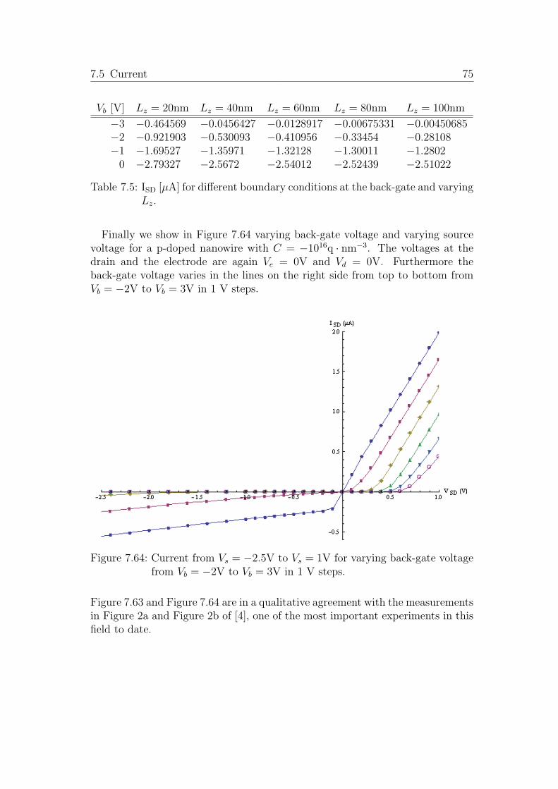
7.5 Current
In order to relate the simulations to measurements, we show the IV characteristicsof the sensor structure. Figure 7.63 shows the source-drain current for varyingback-gate voltage and varying source voltage. Furthermore we set Vd := 0V andVe := 0V. The blue line on the top of the left side of the figure is for Vb = −3V.The lines beneath are for Vb = −2V, Vb = −1V, Vb = 0V, Vb = 1V, Vb = 1.2V,Vb = 1.5V, Vb = 1.8V, and Vb = 2V.
Figure 7.63: Current from Vs = −1V to Vs = 1.4V for varying back-gate voltagefrom Vb = −3V to Vb = 1V in 1 V steps and Vb = 1.2V, Vb = 1.5V,Vb = 1.8V, and Vb = 2V.
Table 7.5 shows the current for different lengths. Here we used Vs = −0.75V,Vd = 0V, and Ve = 0V. We see that the difference between the currents ofbiosensors with Lz = 80nm and Lz = 100nm is for Vb = −3nm bigger than forVb = 0nm.
7.5 Current 75
Vb [V] Lz = 20nm Lz = 40nm Lz = 60nm Lz = 80nm Lz = 100nm
−3 −0.464569 −0.0456427 −0.0128917 −0.00675331 −0.00450685−2 −0.921903 −0.530093 −0.410956 −0.33454 −0.28108−1 −1.69527 −1.35971 −1.32128 −1.30011 −1.2802
0 −2.79327 −2.5672 −2.54012 −2.52439 −2.51022
Table 7.5: ISD [µA] for different boundary conditions at the back-gate and varyingLz.
Finally we show in Figure 7.64 varying back-gate voltage and varying sourcevoltage for a p-doped nanowire with C = −1016q · nm−3. The voltages at thedrain and the electrode are again Ve = 0V and Vd = 0V. Furthermore theback-gate voltage varies in the lines on the right side from top to bottom fromVb = −2V to Vb = 3V in 1 V steps.
Figure 7.64: Current from Vs = −2.5V to Vs = 1V for varying back-gate voltagefrom Vb = −2V to Vb = 3V in 1 V steps.
Figure 7.63 and Figure 7.64 are in a qualitative agreement with the measurementsin Figure 2a and Figure 2b of [4], one of the most important experiments in thisfield to date.

76 7 Simulation and numerical results
7.6 Conclusion
The agreement of Figure 7.63 and 7.64 with measured values shows that theessential physics of field-effect biosensors are included in our PDE-based model.We point out that it is a full 3D model that includes the back-gate contact.This work is therefore an important building block of the self-consistent three-dimensional modeling and simulation of nanowire field-effect biosensors.
The multi-scale problem inherent in these biosensors was solved by implement-ing interface conditions derived from the homogenization of the biofunctional-ized boundary layer. The interface conditions were implemented efficiently bya special numbering scheme of the equations of the discretization. An efficientimplementations is especially important for 3D simulations.
We also investigated how different parameter values for the boundary, the in-terface, and the Na+Cl− concentration influence the source-drain current ISD.The ISD current was calculated because this value is usually measured.
The computation of the macroscopic surface charge density Cs and the macro-scopic dipole moment density D is not discussed in this work. These values havebeen calculated from Poisson-Boltzmann and Monte-Carlo simulations.
In future work we will identify certain physical parameters of BioFETs to ar-rive at a calibrated model and to make predictive simulations of 3D structurespossible.

Bibliography
[1] G. Dahlquist and A. Bjorck, Numerical methods in scientific computing,vol. 1, SIAM, 2008.
[2] C. Heitzinger, N.J. Mauser, and C. Ringhofer, Multi-scale modeling of planarand nanowire field-effect biosensors.
[3] P. Knabner and L. Angermann, Numerik partieller Differentialgleichungen:Eine anwendungsorientierte Einfuhrung, Springer, 2000.
[4] Y. Li, F. Qian, J. Xiang, and C.M. Lieber, Nanowire electronic and opto-electronic devices, Materials today 9 (2006), no. 10, 18–27.
[5] P.A. Markowich, C.A. Ringhofer, and C. Schmeiser, Semiconductor equa-tions, Springer-Verlag New York, Inc. New York, NY, USA, 1990.
[6] F. Patolsky, G. Zheng, and C.M. Lieber, Nanowire sensors for medicine andthe life sciences, Nanomedicine 1 (2006), no. 1, 51–65.
[7] R. Schaback and H. Wendland, Numerische Mathematik, vol. 5, Springer,2005.
[8] D.L. Scharfetter and H.K. Gummel, Large-signal analysis of a silicon readdiode oscillator, IEEE Transactions on Electron Devices 16 (1969), no. 1,64–77.
[9] M.J. Schoning and A. Poghossian, Recent advances in biologically sensitivefield-effect transistors (BioFETs), The Analyst 127 (2002), no. 9, 1137–1151.
[10] M.J. Schoning and A. Poghossian, Bio-feds (field-effect devices): State-of-the-art and new directions, Electroanalysis 18 (2006), 1893–1900.
[11] E. Stern, J.F. Klemic, D.A. Routenberg, P.N. Wyrembak, D.B. Turner-Evans, A.D. Hamilton, D.A. Lavan, T.M. Fahmy, and M.A. Reed, Label-free immunodetection with cmos-compatible semiconducting nanowires, Na-ture(London) 445 (2007), no. 7127, 519–522.

78 Bibliography
[12] E. Stern, E.R. Steenblock, M.A. Reed, and T.M. Fahmy, Label-free elec-tronic detection of the antigen-specific t-cell immune response, Nano Letters8 (2008), no. 10, 3310–3314.
[13] D.R. Thevenot, K. Toth, R.A. Durst, and G.S. Wilson, Electrochemicalbiosensors: recommended definitions and classification, Biosensors and Bio-electronics 16 (2001), no. 1-2, 121–131.
[14] H.A. van der Vorst, Iterative krylov methods for large linear systems, Cam-bridge University Press, 2003.
[15] G. Zheng, F. Patolsky, Y. Cui, W.U. Wang, and C.M. Lieber, Multiplexedelectrical detection of cancer markers with nanowire sensor arrays, Naturebiotechnology 23 (2005), no. 10, 1294–1301.

CURRICULUM VITAE
Stefan Andreas Baumgartner
Geboren am 14. April 1985 in Scheibbs
Staatsburgerschaft: Osterreich
AUSBILDUNG:
November 2007 Abschluss des ersten Studienabschnitts im Diplom-studium Mathematik
Oktober 2005 Beginn der Diplomstudien Mathematik und Musikwis-senschaft
September 2004- April 2005
Prasenzdienst in der Birago Kaserne Melk
Juni 2004 Reifeprufung an der HTBLuVA St.Polten AbteilungEDVO