Embed Size (px)
Citation preview

One-dimensional hole gas in germanium silicon nanowire hetero-structures
Linyou CaoDepartment of Materials Science and Engineering
Drexel University12/09/2005

Motivation-Why?
Quantum Confinement not reported in NW Ballistic Transport Conductance Quantification
Controlled synthesis of NW offering substantial potential to engineer in 1-D electronic system
Band-gap engineering in hetero-system widely used in semiconductor technique
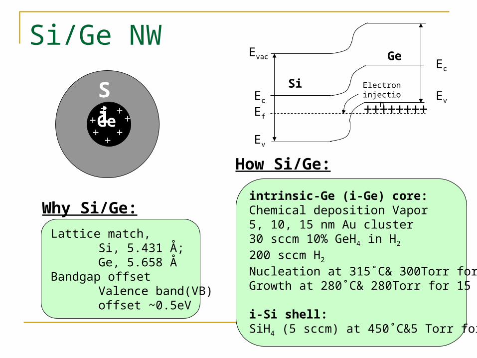
Si/Ge NW
Ge
Si
Ge
SiEc
Ec
Ev
Ev
Ef
Evac
Electron injection
++++++++++
+++
++
Lattice match, Si, 5.431 Å; Ge, 5.658 Å
Bandgap offsetValence band(VB) offset ~0.5eV
Why Si/Ge:intrinsic-Ge (i-Ge) core: Chemical deposition Vapor5, 10, 15 nm Au cluster 30 sccm 10% GeH4 in H2
200 sccm H2
Nucleation at 315˚C& 300Torr for I min Growth at 280˚C& 280Torr for 15 min
i-Si shell: SiH4 (5 sccm) at 450˚C&5 Torr for 5 min
How Si/Ge:

Chemical Vapor Deposition
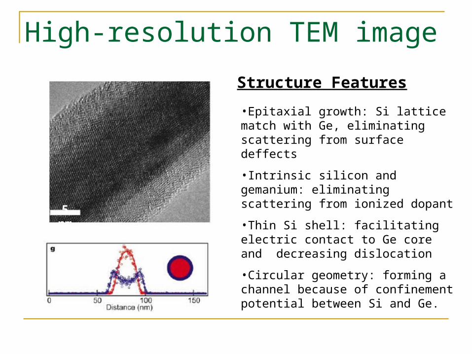
•Epitaxial growth: Si lattice match with Ge, eliminating scattering from surface deffects
•Intrinsic silicon and gemanium: eliminating scattering from ionized dopant
•Thin Si shell: facilitating electric contact to Ge core and decreasing dislocation
•Circular geometry: forming a channel because of confinement potential between Si and Ge.
5 nm
High-resolution TEM image
Structure Features

Fabrication of Devices
50nm Ni
50nm Ni
n-Si R<0.005Ω.cm-1
50 nm SiO2
6nm Al2O3
n-Si R<0.005Ω.cm-1
50 nm SiO2
Top GatedTop Gated
2-5 nm Si /10nm Ge
5~50nm Cr/Au
Annealing: 300oC for 15 min in H2
Electric Measurement enviroment: pressure<10-4 Torr
Back GatedBack Gated

1-D Hole Gas10-nm- Ge(core)/Si(shell) Separate 20-nm Ge or Si
Vg=-10V
Vg=0V
Vg=+10V
Vsd=-1V Vg=-10V
Vg=-10V
Vg=0V
Current increase as Vg changes from -10V to +10V: P-type
Core/shell structure has much larger current: Hole accumulation

Ge
SiEc
Ec
Ev
Ev
Ef
Evac
Electron injection
++++++++Metal
Contact
Schottky contact
Unannealed
Transparent contact
Annealed

Coulomb Blockade-UnneededVg=-9.38 V T=1.5K,
Vsd=0.5mV L=112nm
Unannealed Ge/Si wire, tunnel barrier exists between contact and silicon shell, which acts as Coulomb Island

Coulomb blockade-Conception

Ballistic Transport-Conception
Electron Reservoir
Electron Reservoir1-D conductor
•Finite conductance, which is independent to wire length
•No electron-phonon scattering due to ultra-high velocity of electron
Ballistic Transport
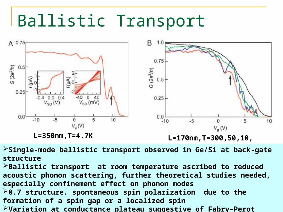
L=350nm,T=4.7K L=170nm,T=300,50,10, 4.7K
Single-mode ballistic transport observed in Ge/Si at back-gate structureBallistic transport at room temperature ascribed to reduced acoustic phonon scattering, further theoretical studies needed, especially confinement effect on phonon modes0.7 structure. spontaneous spin polarization due to the formation of a spin gap or a localized spinVariation at conductance plateau suggestive of Fabry–Perot interferences

Top gate
•Increases the gate coupling, to probe transport through more than one subband.
•Subband observed in G-Vsd (B)
•Subband spacing obtained from transcondutance as functions of Vg and Vsd
•Experiemental value consistent with theoretical calculation based on an effective mass model with a cylindrical confinement potential
5k10k
50k100k

Conclusion
Create a 1D hole gas system in Ge/Si core/shell NW heterostructures.
Ballistic transport through individual 1D subbands due to confinement of carriers in the radial direction
Little temperature dependence, suggesting a room temperature carrier mean free path on the order of several hundred nanometers

Questions:
Physical model for Ge/Si, the effect of depletion thickness of Ge/Si?? Effect of radial size of Ge/Si Effect of spin polarization??
Theoretical Explanation for Ballistic Transport in Si/Ge??

What we can do?? 1-D Electron Gas, inverse Ge/Si??
Controlled 1-D gas via external field, like Quantum Hall Effect
Compound Semiconductor Hetero-Junction??
Multi-layer Junction to make coupled hole-electron,hole-hole,electron-electron gas??
Bipolar transistor, like Optic-electronic

Thanks