Embed Size (px)
Citation preview

Digital Design 2eCopyright © 2010 Frank Vahid
11
Digital Design
Chapter 9:
Hardware Description Languages
Slides to accompany the textbook Digital Design, with RTL Design, VHDL, and Verilog, 2nd Edition,
by Frank Vahid, John Wiley and Sons Publishers, 2010. http://www.ddvahid.com
Copyright © 2010 Frank Vahid
Instructors of courses requiring Vahid's Digital Design textbook (published by John Wiley and Sons) have permission to modify and use these slides for customary course-related activities, subject to keeping this copyright notice in place and unmodified. These slides may be posted as unanimated pdf versions on publicly-accessible course websites.. PowerPoint source (or pdf with animations) may not be posted to publicly-accessible websites, but may be posted for students on internal protected sites or distributed directly to students by other electronic means. Instructors may make printouts of the slides available to students for a reasonable photocopying charge, without incurring royalties. Any other use requires explicit permission. Instructors may obtain PowerPoint source or obtain special use permissions from Wiley – see http://www.ddvahid.com for information.

Digital Design 2eCopyright © 2010 Frank Vahid
2
Introduction
• A drawing of a circuit, or schematic, contains graphical information about a design– Inverter is above the OR gate,
AND gate is to the right, etc.
• Such graphical information may not be useful for large designs
• Can use textual language instead
9.1
si
gtocontr
atapa
DoorOpener
c
h
p
f
Note: Slides with animation are denoted with a small red "a" near the animated items

Digital Design 2eCopyright © 2010 Frank Vahid
3
Textual Language – English• Can describe circuit using English text rather than using a drawing
– Of course, English isn't a good language for a computer to read– Need a more precise, computer-oriented language
DoorOpener
c
h
p
f
AND2_1OR2_1
Inv_1
n2
n1
(a) (b) We'll now describe a circuit whose name isDoorOpener.Theexternal inputs arec, h andp, which are bits.Theexternal output isf, which is a bit.
We assumeyouknow the behavior of thesecomponents:An inverter, which has a bit input x, and bit outputF.
A 2-input OR gate, which has inputs x andy, and bit outputF. A 2-input AND gate, which has bit inputs x andy, and bit outputF.
The circuit has internal wires n1 and n2, both bits.TheDoorOpener circuit internallyconsists of:
An inverter named Inv_1, whose input xconnectstoexternal input c, and whose outputconnectsto n1.
A 2-input OR gate named OR2_1, whose inputsconnect toexternal inputs h andp, and whose outputconnectsto n2. A 2-input AND gate named AND2_1, whose inputsconnect to n1 and n2, and whose outputconnectstoexternal outputf.That's all.

Digital Design 2eCopyright © 2010 Frank Vahid
4
Computer-Readable Textual Language for Describing Hardware Circuits: HDLs
• Hardware description language (HDL) – Intended to describe circuits textually, for a computer to read– Evolved starting in the 1970s and 1980s
• Popular languages today include:– VHDL –Defined in 1980s by U.S. military; Ada-like language– Verilog –Defined in 1980s by a company; C-like language– SystemC –Defined in 2000s by several companies; consists of
libraries in C++

Digital Design 2eCopyright © 2010 Frank Vahid
5
Combinational Logic Description using Hardware Description Languages
• Structure– Another word for "circuit"– An interconnection of
components– Key use of HDLs is to describe
structure
9.2
DoorOpener
c
h
p
f
Note: The term "instantiate" will be used to indicate adding a new copy of a component to a circuit
OR_2OR_1
OR_3
The OR component Three instances of the OR component

Digital Design 2eCopyright © 2010 Frank Vahid
6
Describing Structure in VHDL• Entity – Defines new
item's name & ports (inputs/outputs)– std_logic means bit
type, defined in ieee library
• Architecture – Describes internals, which we named "Circuit"– Declares 3 previously-
defined components– Declares internal
signals• Note "--" comment
– Instantiates and connects those components
DoorOpener
c
h
p
f
AND2_1OR2_1
Inv_1
n2
n1
(a)
(b) (c)
We'll now describe a circuit whose name is DoorOpener. The external inputs are c, h and p, which are bits. The external output is f, which is a bit.
We assume you know the behavior of these components: An inverter, which has a bit input x, and bit output F. A 2-input OR gate, which has inputs x and y, and bit output F. A 2-input AND gate, which has bit inputs x and y, and bit output F.
The circuit has internal wires n1 and n2, both bits.
The DoorOpener circuit internally consists of: An inverter named Inv_1, whose input x connects to external input c, and whose output connects to n1. A 2-input OR gate named OR2_1, whose inputs connect to external inputs h and p, and whose output connects to n2. A 2-input AND gate named AND2_1, whose inputs connect to n1 and n2, and whose output connects to external output f.That's all.
library ieee;use ieee.std_logic_1164.all;entity DoorOpener is
port ( c, h, p: in std_logic; f: out std_logic );end DoorOpener;
architecture Circuit of DoorOpener iscomponent Inv
port (x: in std_logic; F: out std_logic);
end component;component OR2
port (x,y: in std_logic; F: out std_logic);
end component;component AND2
port (x,y: in std_logic; F: out std_logic);
end component;signal n1,n2: std_logic; --internal wires
begin Inv_1: Inv port map (x=>c, F=>n1); OR2_1: OR2 port map (x=>h,y=>p,F=>n2); AND2_1: AND2

Digital Design 2eCopyright © 2010 Frank Vahid
7
Describing Structure in Verilog• Modules defined for
Inv, OR2, and AND2 (details omitted)– Note "//" comment
• Module defined for DoorOpener– Lists inputs and
outputs – Declares internal
wires– Instantiates and
connects three components
DoorOpener
c
h
p
f
AND2_1OR2_1
Inv_1
n2
n1
(a)
(b) (c)
We'll now describe a circuit whose name is DoorOpener. The external inputs are c, h and p, which are bits. The external output is f, which is a bit.
We assume you know the behavior of these components: An inverter, which has a bit input x, and bit output F. A 2-input OR gate, which has inputs x and y, and bit output F. A 2-input AND gate, which has bit inputs x and y, and bit output F.
The circuit has internal wires n1 and n2, both bits.
The DoorOpener circuit internally consists of: An inverter named Inv_1, whose input x connects to external input c, and whose output connects to n1. A 2-input OR gate named OR2_1, whose inputs connect to external inputs h and p, and whose output connects to n2. A 2-input AND gate named AND2_1, whose inputs connect to n1 and n2, and whose output connects to external output f.That's all.
module Inv(x, F);input x;output F;
// details not shownendmodulemodule OR2(x, y, F);
input x, y;output F;
// details not shownendmodulemodule AND2(x, y, F);
input x, y;output F;
// details not shownendmodule
module DoorOpener(c, h, p, f);input c, h, p;output f;wire n1, n2;
Inv Inv_1(c, n1); OR2 OR2_1(h, p, n2); AND2 AND2_1(n1, n2, f);

Digital Design 2eCopyright © 2010 Frank Vahid
8
Describing Structure in SystemC• Module defined
– Declares inputs and outputs
– Declares internal wires
• Note "//" comment
– Declares three previously-defined components
– Constructor function "CTOR"
• Instantiates components
• Connects components
DoorOpener
c
h
p
f
AND2_1OR2_1
Inv_1
n2
n1
(a)
(b) (c)
We'll now describe a circuit whose name is DoorOpener. The external inputs are c, h and p, which are bits. The external output is f, which is a bit.
We assume you know the behavior of these components: An inverter, which has a bit input x, and bit output F. A 2-input OR gate, which has inputs x and y, and bit output F. A 2-input AND gate, which has bit inputs x and y, and bit output F.
The circuit has internal wires n1 and n2, both bits.
The DoorOpener circuit internally consists of: An inverter named Inv_1, whose input x connects to external input c, and whose output connects to n1. A 2-input OR gate named OR2_1, whose inputs connect to external inputs h and p, and whose output connects to n2. A 2-input AND gate named AND2_1, whose inputs connect to n1 and n2, and whose output connects to external output f.That's all.
#include "systemc.h"#include "inv.h"#include "or2.h"#include "and2.h"
SC_MODULE (DoorOpener){
sc_in<sc_logic> c, h, p;sc_out<sc_logic> f;
// internal wiressc_signal<sc_logic> n1, n2;
// component declarations Inv Inv1; OR2 OR2_1; AND AND2_1; // component instantiations
SC_CTOR(DoorOpener):Inv_1("Inv_1"), OR2_1("OR2_1"), AND2_1("AND2_1") { Inv_1.x(c); Inv_1.F(n1); OR2_1.x(h); OR2_1.y(p); OR2_1.F(n2); AND2_1.x(n1); AND2_1.y(n2); AND2_1.F(f); }};

Digital Design 2eCopyright © 2010 Frank Vahid
9
Combinational Behavior
• Combinational behavior– Description of desired behavior of combinational circuit without
creating circuit itself– e.g., F = c' * (h + p) can be described as equation rather than circuit– HDLs support description of combinational behavior

Digital Design 2eCopyright © 2010 Frank Vahid
10
Describing Combinational Behavior in VHDL• Describing an OR gate's
behavior– Entity defines input/output ports– Architecture
• Process – Describes behavior– Process "sensitive" to x and y
» Means behavior only executes when x changes or y changes
– Behavior assigns a new value to output port F, computed using built-in operator "or"
library ieee;use ieee.std_logic_1164.all;
entity OR2 isport (x, y: in std_logic;
F: out std_logic );end OR2;
architecture behavior of OR2 isbeginprocess (x, y)begin
F <= x or y;end process;
end behavior;

Digital Design 2eCopyright © 2010 Frank Vahid
11
Describing Combinational Behavior in VHDL• Describing a custom
function's behavior– Desired function: f = c'*(h+p)– Entity defines input/output ports
(not shown)– Architecture
• Process– Sensitive to c, h, and p– Assigns a new value to output
port f, computed using built-in operators "not", "and", and "or"
architecture beh of DoorOpener isbeginprocess(c, h, p) begin f <= not(c) and (h or p);end process;
end beh;

Digital Design 2eCopyright © 2010 Frank Vahid
12
Describing Combinational Behavior in Verilog• Describing an OR gate's
behavior– Module declares input/output
ports• Also indicates that F is "reg"• Means F stores value
– By default, ports are wires, having no storage
– "always" procedure executes statement block when change occurs on x or on y
• "Sensitive" to x and y• Assigns value to F, computed
using built-in OR operator "|"
module OR2(x,y,F);input x, y;output F;reg F;
always @(x or y)begin
F <= x | y;end
endmodule

Digital Design 2eCopyright © 2010 Frank Vahid
13
Describing Combinational Behavior in Verilog• Describing a custom
function's behavior– Desired function: f = c'*(h+p)– Module defines input/output
ports• Output f defined as "reg"
– "always" procedure sensitive to inputs
• Assigns value to f, computed using built-in operators for NOT (~), AND (&), and OR (|)
module DoorOpener(c,h,p,f);input c, h, p;output f;reg f;
always @(c or h or p)begin
f <= (~c) & (h | p);end
endmodule

Digital Design 2eCopyright © 2010 Frank Vahid
14
Describing Combinational Behavior in SystemC• Describing an OR gate's
behavior– Module declares input/output
ports– Constructor (CTOR)
• Indicates module described by a method (procedure) "comblogic"
• Sensitive to x and y– Method "comblogic" assigns F a
new value using built-in OR operator "|"
• Reading input port done using .read() function defined for input port type; likewise, writing done using .write() function
#include "systemc.h"
SC_MODULE(OR2){sc_in<sc_logic> x, y; sc_out<sc_logic> F;
SC_CTOR(OR2) {
SC_METHOD(comblogic);sensitive << x << y;
}
void comblogic() { F.write(x.read() | y.read()); }};

Digital Design 2eCopyright © 2010 Frank Vahid
15
Describing Combinational Behavior in SystemC• Describing a custom function's
behavior– Desired function: f = c'*(h+p)– Module defines input/output ports– Constructor
• Indicates module described by a method (procedure) "comblogic"
• Sensitive to c, h, and p– "comblogic" method
• Assigns value to f, computed using built-in operators for NOT (~), AND (&), and OR (|)
#include "systemc.h"
SC_MODULE(DoorOpener){
sc_in<sc_logic> c, h, p; sc_out<sc_logic> f;
SC_CTOR(DoorOpener) {
SC_METHOD(comblogic);sensitive << c << h << p;
}
void comblogic() { f.write((~c.read()) & (h.read() | p.read

Digital Design 2eCopyright © 2010 Frank Vahid
16
Testbenches• Testbench
– Assigns values to a system's inputs, check that system outputs correct values
– A key use of HDLs is to simulate system to ensure design is correct
SystemToTest
Testbench
Set input values, check output values

Digital Design 2eCopyright © 2010 Frank Vahid
17
Testbench in VHDL• Entity
– No inputs or outputs• Architecture
– Declares component to test, declares signals
– Instantiates component, connects to signals
– Process writes input signals, checks output signal
• Waits a small amount of time after writing input signals
• Checks for correct output value using "assert" statement
library ieee;use ieee.std_logic_1164.all;
entity Testbench isend Testbench;
architecture behavior of Testbench iscomponent DoorOpenerport ( c, h, p: in std_logic;
f: out std_logic );end component;signal c, h, p, f: std_logic;
begin DoorOpener1: DoorOpener port map (c,h,p,f);
processbegin
-- case 0 c <= '0'; h <= '0'; p <= '0';
wait for 1 ns;assert (f='0') report "Case 0 failed";
-- case 1 c <= '0'; h <= '0'; p <= '1';
wait for 1 ns;assert (f='1') report "Case 1 failed";
-- (cases 2-6 omitted from figure) -- case 7 c <= '1'; h <= '1'; p <= '1';
wait for 1 ns;assert (f='0') report
SystemToTest
Testbench
Set input values, check output values
process
DoorOpener1

Digital Design 2eCopyright © 2010 Frank Vahid
18
Testbench in Verilog• Module
– Three register signals for inputs (values must be written and stored)
– One wire signal for output (value is only read, need not be stored)
– Instantiates component, connects to signals
– "initial" procedure executed only once at beginning
• Sets input values• Displays output value
SystemToTest
Testbench
Set input values, check output values
"initial" procedure
module Testbench;reg c, h, p;wire f;
DoorOpener DoorOpener1(c, h, p, f);
initial begin // case 0 c <= 0; h <= 0; p <= 0;
#1 $display("f = %b", f); // case 1 c <= 0; h <= 0; p <= 1;
#1 $display("f = %b", f); // (cases 2-6 omitted from figure) // case 7 c <= 1; h <= 1; p <= 1;
#1 $display("f = %b", f);DoorOpener1

Digital Design 2eCopyright © 2010 Frank Vahid
19
Testbench in SystemC• Module
– Testbench is its own module– Three outputs, one for each input
of system to test– One input, for the one output of
the system to test– Constructor defined as THREAD
• Like MODULE, but allows use of "wait" to control timing
– testbench procedure writes outputs, waits for small amount of time, checks for correct output
• assert function prints error if condition is not true
SystemToTest
Set input values, check output values
Testbench
DoorOpener1
#include "systemc.h"
SC_MODULE(Testbench){sc_out<sc_logic> c_t, h_t, p_t;sc_in<sc_logic> f_t;
SC_CTOR(Testbench) {
SC_THREAD(testbench_proc); }
void testbench_proc() { // case 0 c_t.write(SC_LOGIC_0); h_t.write(SC_LOGIC_0); p_t.write(SC_LOGIC_0);
wait(1, SC_NS);assert( f_t.read() == SC_LOGIC_0 );
// case 1 c_t.write(SC_LOGIC_0); h_t.write(SC_LOGIC_0); p_t.write(SC_LOGIC_1);
wait(1, SC_NS);assert( f_t.read() == SC_LOGIC_1 );
// (cases 2-6 omitted from figure) // case 7 c_t.write(SC_LOGIC_1); h_t.write(SC_LOGIC_1); p_t.write(SC_LOGIC_1);
wait(1, SC_NS);assert( f_t.

Digital Design 2eCopyright © 2010 Frank Vahid
20
Sequential Logic Description using Hardware Description Languages
• Will consider description of three sequential components– Registers– Oscillators– Controllers
9.3

Digital Design 2eCopyright © 2010 Frank Vahid
21
Describing a 4-bit Register in VHDL• Entity
– 4 data inputs, 4 data outputs, and a clock input
– Use std_logic_vector for 4-bit data• I: in std_logic_vector(3 downto 0)• I <= "1000" would assign I(3)=1,
I(2)=0, I(1)=0, I(0)=0
• Architecture– Process sensitive to clock input
• First statement detects if change on clock was a rising edge
• If clock change was rising edge, sets output Q to input I
• Ports are signals, and signals store values – thus, output retains new value until set to another value
library ieee;use ieee.std_logic_1164.all;
entity Reg4 is port ( I: in std_logic_vector(3 downto 0); Q: out std_logic_vector(3 downto 0); clk: in std_logic );end Reg4;
architecture behavior of Reg4 isbegin
process(clk)begin
if (clk='1' and clk'event) then Q <= I;
end if

Digital Design 2eCopyright © 2010 Frank Vahid
22
Describing a 4-bit Register in Verilog• Module
– 4 data inputs, 4 data outputs, and a clock input
– Define data inputs/outputs as vectors
• input [3:0] I• I<=4'b1000 assigns I[3]=1,
I[2]=0, I[1]=0, I[0]=0• Output defined as register to
store value– "always" procedure sensitive to
positive (rising) edge of clock• Sets output Q to input I
module Reg4(I, Q, clk);input [3:0] I;input clk;output [3:0] Q;reg [3:0] Q;
always @(posedge clk)begin
Q <= I;

Digital Design 2eCopyright © 2010 Frank Vahid
23
Describing a 4-bit Register in SystemC• Module
– 4 data inputs, 4 data outputs, and a clock input
– Define data inputs/outputs as vectors
• sc_in<sc_lv<4> > I;• I<=“1000" assigns I[3]=1,
I[2]=0, I[1]=0, I[0]=0– Constructor calls seq_logic
method, sensitive to positive (rising) edge of clock
• seq_logic writes output Q with input I
• Output port is signal, and signal has storage, thus output retains value
#include "systemc.h"
SC_MODULE(Reg4){
sc_in<sc_lv<4> > I;sc_out<sc_lv<4> > Q;sc_in<sc_logic> clk;
SC_CTOR(Reg4) {
SC_METHOD(seq_logic);sensitive_pos << clk;
}
void seq_logic() { Q.

Digital Design 2eCopyright © 2010 Frank Vahid
24
Describing an Oscillator in VHDL• Entity
– Defines clock output
• Architecture– Process
• Has no sensitivity list, so executes non-stop as infinite loop
• Sets clock to 0, waits 10 ns, sets clock to 1, waits 10 ns, repeats
library ieee;use ieee.std_logic_1164.all;
entity Osc isport ( clk: out std_logic );
end Osc;
architecture behavior of Osc isbegin
processbegin
clk <= '0';wait for 10 ns;
clk <= '1';wait for 10 ns;

Digital Design 2eCopyright © 2010 Frank Vahid
25
Describing an Oscillator in Verilog• Module
– Has one output, clk• Declare as "reg" to hold value
– "always" procedure• Has no sensitivity list, so
executes non-stop as infinite loop
• Sets clock to 0, waits for 10 ns, sets clock to 1, waits for 10 ns, repeats
module Osc(clk);output clk;reg clk;
always begin clk <= 0;
#10; clk <= 1;
#10;end
endmodule
Digital Design 2eCopyright © 2010 Frank Vahid
26
Describing an Oscillator in SystemC• Module
– Has one output, clk– Constructor creates single
thread• Thread consists of infinite loop
– while (true) {• Sets clock to 0, waits 10 ns,
sets clock to 1, waits 10 ns, repeats
#include "systemc.h"
SC_MODULE(Osc){
sc_out<sc_logic> clk;
SC_CTOR(Osc) {
SC_THREAD(seq_logic); }
void seq_logic() {
while(true) { clk.write(SC_LOGIC_0);
wait(10, SC_NS); clk.write(SC_LOGIC_1);

Digital Design 2eCopyright © 2010 Frank Vahid
27
Describing a Controller in VHDL
Inputs: b; Outputs: x
On2On1 On3
Off
x=1x=1x=1
x=0
b’
b
library ieee;use ieee.std_logic_1164.all
entity LaserTimer isport (b: in std_logic;
x: out std_logic; clk, rst: in std logic );end LaserTimer;
architecture behavior of LaserTimer istype statetype is
(S_Off, S_On1, S_On2, S_On3);signal currentstate, nextstate:
statetype;begin statereg: process(clk, rst)
beginif (rst='1') then -- intial state
currentstate <= S_Off;elsif (clk='1' and clk'event) then
currentstate <= nextstate;end if;
end process;
comblogic: process (currentstate, b)begin
case currentstate iswhen S_Off =>
x <= '0'; -- laser offif (b='0') then
nextstate <= S_Off;else
nextstate <= S_On1;end if;
when S_On1 => x <= '1'; -- laser on nextstate <= S_On2;
when S_On2 => x <= '1'; -- laser still on nextstate <= S_On3;
• FSM behavior captured using architecture with 2 processes– First process models state register
• Asynchronous reset sets state to "S_Off"• Rising clock edge sets currentstate to
nextstate– Second process models combinational logic
• Sensitive to currentstate and FSM inputs• Sets FSM outputs based on currentstate• Sets nextstate based on currentstate and
present FSM input values– Note declaration of new type, statetype
Combinationallogic
State register
s1 s0
n1
n0
xb
clk
FSM
inp
uts
FSM
ou
tpu
ts

Digital Design 2eCopyright © 2010 Frank Vahid
28
Describing a Controller in Verilog
Inputs: b; Outputs: x
On2On1 On3
Off
x=1x=1x=1
x=0
b’
b
• FSM behavior captured using 2 "always" procedures– First procedure models state register
• Asynchronous reset sets state to "S_Off"• Rising clock edge sets currentstate to
nextstate– Second process models combinational logic
• Sensitive to currentstate and FSM inputs• Sets FSM outputs based on currentstate• Sets nextstate based on currentstate and
present FSM input values– Note state register size must be explicit – 2
bits, reg [1:0] currentstate
Combinationallogic
State register
s1 s0
n1
n0
xb
clk
FSM
inp
uts
FSM
ou
tpu
ts
module LaserTimer(b, x, clk, rst);input b, clk, rst;output x;reg x;
parameter S_Off = 2'b00, S_On1 = 2'b01, S_On2 = 2'b10, S_On3 = 2'b11;
reg [1:0] currentstate;reg [1:0] nextstate;
// state register procedurealways @(posedge rst or posedge clk)begin
if (rst==1) // initial state currentstate <= S_Off;
else currentstate <= nextstate;
end // combinational logic procedure
always @(currentstate or b)begin
case (currentstate) S_Off: begin x <= 0; // laser off
if (b==0) nextstate <= S_Off;
else nextstate <= S_On1;
end S_On1: begin x <= 1; // laser on nextstate <= S_On2;
end S_On2: begin x <= 1; // laser still on nextstate <= S_On3;
end

Digital Design 2eCopyright © 2010 Frank Vahid
29
Describing a Controller in SystemC
Inputs: b; Outputs: x
On2On1 On3
Off
x=1x=1x=1
x=0
b’
b
• FSM behavior captured using 2 methods– First method models state register
• Asynchronous reset sets state to "S_Off"• Rising clock edge sets currentstate to
nextstate– Second process models combinational logic
• Sensitive to currentstate and FSM inputs• Sets FSM outputs based on currentstate• Sets nextstate based on currentstate and
present FSM input values– Note use of new type, statetype
Combinationallogic
State register
s1 s0
n1
n0
xb
clk
FSM
inp
uts
FSM
ou
tpu
ts
#include "systemc.h"
enum statetype { S_Off, S_On1, S_On2, S_On3 };
SC_MODULE(LaserTimer){sc_in<sc_logic> b, clk, rst;sc_out<sc_logic> x;sc_signal<statetype> currentstate, nextstate;
SC_CTOR(LaserTimer) {SC_METHOD(statereg);sensitive_pos << rst << clk;SC_METHOD(comblogic);sensitive << currentstate << b;
}
void statereg() {if( rst.read() == SC_LOGIC_1 )
currentstate = S_Off; // initial stateelse
currentstate = nextstate; }void comblogic() {switch (currentstate) {case S_Off:
x.write(SC_LOGIC_0); // laser offif( b.read() == SC_LOGIC_0 )
nextstate = S_Off;else
nextstate = S_On1;break;
case S_On1: x.write(SC_LOGIC_1); // laser on nextstate = S_On2;
break;case S_On2:
x.write(SC_LOGIC_1); // laser still on nextstate = S_On3;
break;

Digital Design 2eCopyright © 2010 Frank Vahid
30
Datapath Component Description using Hardware Description Languages
• Will consider description of three datapath components– Full-adders– Carry-ripple adders– Up-counter
9.4

Digital Design 2eCopyright © 2010 Frank Vahid
31
Describing a Full-Adder in VHDL• Entity
– Declares inputs/outputs
• Architecture– Described
behaviorally (could have been described structurally)
– Process sensitive to inputs
– Computes expressions, sets outputs
library ieee;use ieee.std_logic_1164.all;
entity FullAdder isport ( a, b, ci: in std_logic;
s, co: out std_logic );end FullAdder;
architecture behavior of FullAdder isbegin
process (a, b, ci)begin
s <= a xor b xor ci; co <= (b and ci) or (a and ci) or (a and
s = a xor b xor cico = bc + ac + ab
co
ciba
s
Full adder

Digital Design 2eCopyright © 2010 Frank Vahid
32
Describing a Full-Adder in Verilog• Module
– Declares inputs/outputs– Described behaviorally (could
have been described structurally)
– "always" procedure• Sensitive to inputs
– Computes expressions, sets outputs
s = a xor b xor cico = bc + ac + ab
co
ciba
s
Full adder
module FullAdder(a, b, ci, s, co);input a, b, ci;output s, co;reg s, co;
always @(a or b or ci)begin
s <= a ^ b ^ ci; co <= (b & ci) | (a & ci) | (a & b);
Digital Design 2eCopyright © 2010 Frank Vahid
33
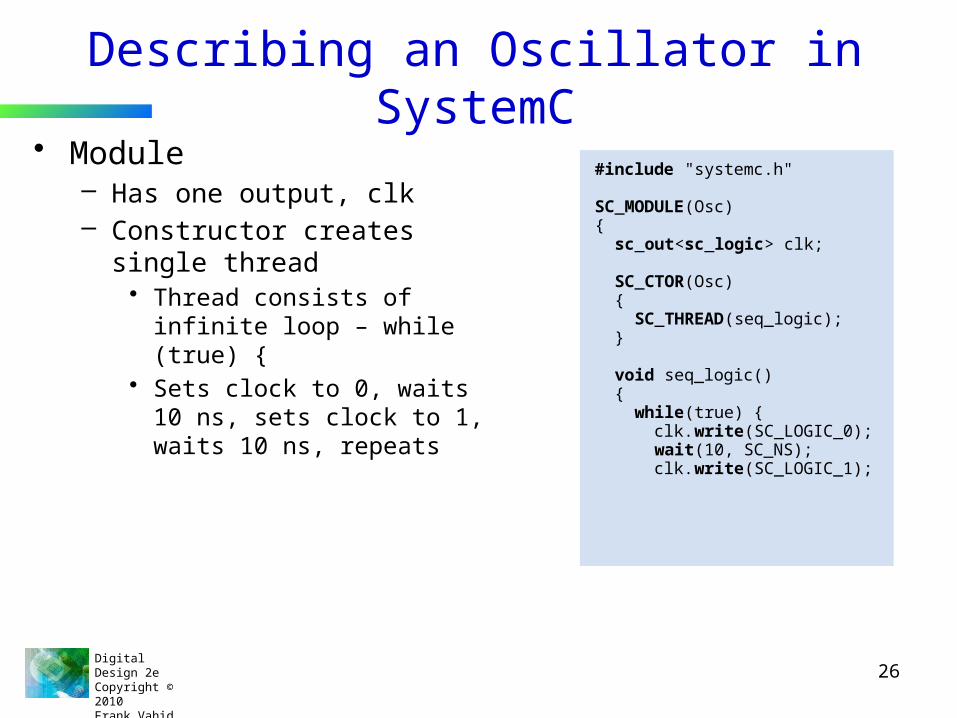
Describing a Full-Adder in SystemC• Module
– Declares inputs/outputs
– Described behaviorally (could have been described structurally)
– comblogic method• Computes
expressions, sets outputs
s = a xor b xor cico = bc + ac + ab
co
ciba
s
Full adder
#include "systemc.h"
SC_MODULE(FullAdder){sc_in<sc_logic> a, b, ci;sc_out<sc_logic> s, co;
SC_CTOR(FullAdder) {
SC_METHOD(comblogic);sensitive << a << b << ci;
}
void comblogic() { s.write(a.read() ^ b.read() ^ ci.read()); co.write((b.read() & ci.read()) | (a.read() & ci.read()) | (a.read() & b.read())); }};

Digital Design 2eCopyright © 2010 Frank Vahid
34
Describing a Carry-Ripple Adder in VHDL• Entity
– Declares inputs/outputs– Uses std_logic_vector for
4-bit inputs/outputs• Architecture
– Described structurally by composing four full-adders (could have been described behaviorally instead)
– Declares full-adder component, instantiates four full-adders, connects
• Note use of three internal signals for connecting carry-out of one stage to carry-in of next stage
library ieee;use ieee.std_logic_1164.all;
entity CarryRippleAdder4 isport ( a: in std_logic_vector(3 downto 0);
b: in std_logic_vector(3 downto 0); ci: in std_logic; s: out std_logic_vector(3 downto 0); co: out std_logic );end CarryRippleAdder4;
architecture structure of CarryRippleAdder4 iscomponent FullAdder
port ( a, b, ci: in std_logic; s, co: out std_logic );
end component;signal co1, co2, co3: std_logic;
begin FullAdder1: FullAdder
port map (a(0), b(0), ci, s(0), co1); FullAdder2: FullAdder
port map (a(1), b(1), co1, s(1), co2); FullAdder3: FullAdder
a3
co s
FA
co
b3 a2b2
s3 s2 s1
ciba
co s
FA
ciba
a1b1
co s
FA
ciba
s0
a0b0 ci
co s
FA
ciba
co1co2co3

Digital Design 2eCopyright © 2010 Frank Vahid
35
Describing a Carry-Ripple Adder in Verilog• Module
– Declares inputs/outputs– Uses vectors for 4-bit
inputs/outputs– Described structurally by
composing four full-adders (could have been described behaviorally instead)
– Instantiates four full-adders, connects
• Note use of three internal wires for connecting carry-out of one stage to carry-in of next stage
a3
co s
FA
co
b3 a2b2
s3 s2 s1
ciba
co s
FA
ciba
a1b1
co s
FA
ciba
s0
a0b0 ci
co s
FA
ciba
module CarryRippleAdder4(a, b, ci, s, co);input [3:0] a;input [3:0] b;input ci;
output [3:0] s;output co;
wire co1, co2, co3;
FullAdder FullAdder1(a[0], b[0], ci, s[0], co1); FullAdder FullAdder2(a[1], b[1], co1, s[1], co2); FullAdder FullAdder3(a[2], b[2], co2, s[2], co3); FullAdder FullAdder4(a[3], b[3], co3, s[3], co);
co1co2co3

Digital Design 2eCopyright © 2010 Frank Vahid
36
Describing a Carry-Ripple Adder in SystemC#include "systemc.h"#include "fulladder.h"
SC_MODULE(CarryRippleAdder4){
sc_in<sc_logic> a[4];sc_in<sc_logic> b[4];sc_in<sc_logic> ci;sc_out<sc_logic> s[4];sc_out<sc_logic> co;
sc_signal<sc_logic> co1, co2, co3;
FullAdder FullAdder_1; FullAdder FullAdder_2; FullAdder FullAdder_3; FullAdder FullAdder_4;
SC_CTOR(CarryRipple4): FullAdder_1("FullAdder_1"), FullAdder_2("FullAdder_2"), FullAdder_3("FullAdder_3"), FullAdder_4("FullAdder_4") { FullAdder_1.a(a[0]); FullAdder_1.b(b[0]); FullAdder_1.ci(ci); FullAdder_1.s(s[0]); FullAdder_1.co(co1);
FullAdder_2.a(a[1]); FullAdder_2.b(b[1]); FullAdder_2.ci(co1); FullAdder_2.s(s[1]);
a3
co s
FA
co
b3 a2b2
s3 s2 s1
ciba
co s
FA
ciba
a1b1
co s
FA
ciba
s0
a0b0 ci
co s
FA
ciba
co1co2co3
• Module– Declares
inputs/outputs– Uses vectors for 4-bit
inputs/outputs– Described structurally
by composing four full-adders (could have been described behaviorally instead)
– Instantiates four full-adders, connects
• Note use of three internal wires for connecting carry-out of one stage to carry-in of next stage

Digital Design 2eCopyright © 2010 Frank Vahid
37
Describing an Up-Counter in VHDL
• Described structurally (could have been described behaviorally)
• Includes process that updates output port C whenever internal signal tempC changes– Need tempC signal because
can't read C due to C being an output port
ld4-bit register
Ctc
4
4 4
4
cnt
4-bit up-counter
+1
library ieee;use ieee.std_logic_1164.all;
entity UpCounter isport ( clk: in std_logic;
cnt: in std_logic; C: out std_logic_vector(3 downto 0); tc: out std_logic );end UpCounter;
architecture structure of UpCounter iscomponent Reg4
port ( I: in std_logic_vector(3 downto 0); Q: out std_logic_vector(3 downto 0); clk, ld: in std_logic );
end component; component Inc4
port ( a: in std_logic_vector(3 downto 0); s: out std_logic_vector(3 downto 0) );
end component;component AND4
port ( w,x,y,z: in std_logic; F: out std_logic );
end component;signal tempC: std_logic_vector(3 downto 0);signal incC: std_logic_vector(3 downto 0);
begin Reg4_1: Reg4 port map(incC, tempC, clk, cnt); Inc4_1: Inc4 port map(tempC, incC); AND4_1: AND4 port map(tempC(3), tempC(2),
tempC

Digital Design 2eCopyright © 2010 Frank Vahid
38
Describing an Up-Counter in Verilog
• Described structurally (could have been described behaviorally)
• Includes always procedure that updates output C whenever internal wire tempC changes– Need tempC wire because
can't use C in the connection statements
ld4-bit register
Ctc
4
4 4
4
cnt
4-bit up-counter
+1tempC
module Reg4(I, Q, clk, ld);input [3:0] I;input clk, ld;output [3:0] Q;
// details not shownendmodule
module Inc4(a, s);input [3:0] a;output [3:0] s;
// details not shownendmodule
module AND4(w,x,y,z,F);input w, x, y, z;output F;
// details not shownendmodule
module UpCounter(clk, cnt, C, tc);input clk, cnt;output [3:0] C;reg [3:0] C;output tc;
wire [3:0] tempC;wire [3:0] incC;
Reg4 Reg4_1(incC, tempC, clk, cnt); Inc4 Inc4_1(tempC, incC); AND4 AND4_1(tempC[3], tempC[2], tempC[1], tempC[0], tc);
always @

Digital Design 2eCopyright © 2010 Frank Vahid
39
Describing an Up-Counter in SystemC
• Described structurally (could have been described behaviorally)
• Includes method that updates output C whenever internal signal tempC changes– Need tempC signal because can't
use C in the connection statements• Can't use logic vector bits
individually for connections, so needed tempC_b array too
ld4-bit register
Ctc
4
4 4
4
cnt
4-bit up-counter
+1tempC
#include "systemc.h"#include "reg4.h"#include "inc4.h"#include "and4.h"
SC_MODULE(UpCounter){
sc_in<sc_logic> clk, cnt;sc_out<sc_lv<4> > C;sc_out<sc_logic> tc;
sc_signal<sc_lv<4> > tempC, incC;sc_signal<sc_logic> tempC_b[4];
Reg4 Reg4_1; Inc4 Inc4_1; AND4 AND4_1;
SC_CTOR(UpCounter) : Reg4_1("Reg4_1"), Inc4_1("Inc4_1"), AND4_1("AND4_1") { Reg4_1.I(incC); Reg4_1.Q(tempC); Reg4_1.clk(clk); Reg4_1.ld(cnt);
Inc4_1.a(tempC); Inc4_1.s(incC);
AND4_1.w(tempC_b[0]); AND4_1.x(tempC_b[1]); AND4_1.y(tempC_b[2]); AND4_1.z(tempC_b[3]); AND4_1.F(tc);
SC_METHOD(comblogic);sensitive << tempC;
}
void comblogic() { tempC_b[0] = tempC.read()[0]; tempC_b[1] = tempC.read()[1]; tempC_b[2] = tempC.read

Digital Design 2eCopyright © 2010 Frank Vahid
40
RTL Design using Hardware Description Languages
• Will consider two forms of RTL descriptions– High-level state machine– Controller and datapath
9.5

Digital Design 2eCopyright © 2010 Frank Vahid
41
HLSM of Laser-Based Dist. Measurer: VHDL
• Architecture similar to FSM– Curr/next sigs
for all regs• Asynch reset
forces to state S0• Rising clock
– Perform state's computation
– Prepare to go to next state based on state and inputs
• Concurrent sig assignment sets D to Dreg always
library IEEE;use IEEE.STD_LOGIC_1164.ALL;use IEEE.STD_LOGIC_ARITH.ALL;use IEEE.STD_LOGIC_UNSIGNED.ALL;
entity LaserDistMeasurer isport (
clk, rst : in std_logic; B, S : in std_logic; L : out std_logic; D : out std_logic_vector
(15 downto 0));end LaserDistMeasurer;
architecture behavior of LaserDistMeasurer is
type statetype is (S0,S1,S2,S3,S4);signal State, StateNext : statetype;
signal Dctr, DctrNext:std_logic_vector(15 downto 0);
signal Dreg, DregNext:std_logic_vector(15 downto 0);
constant U_ZERO :std_logic_vector(15 downto 0)
:= "0000000000000000";constant U_ONE :
std_logic_vector(15 downto 0):= "0000000000000001";
begin
Regs: process(clk, rst)begin
if(rst = '1') then State <= S0; Dctr <= U_ZERO; Dreg <= U_ZERO;
elsif(clk'event and clk='1') then State <= StateNext; Dctr <= DctrNext; Dreg <= DregNext;
end if;end process;
CombLogic: process(State, Dctr, B, S)begin
case State iswhen S0 =>
L <= '0'; -- laser off DregNext <= U_ZERO; --clr D DctrNext <= U_ZERO; --clr Dctr StateNext <= S1;
when S1 => DctrNext <= U_ZERO; --clr Dctr L <= '0'; -- laser off
if(B = '1') then StateNext <= S2;
else StateNext <= S1;
end if;when S2 =>
L <= '1'; --laser on DctrNext <= U_ZERO; StateNext <= S3;
when S3 => L <= '0'; -- laser off DctrNext <= Dctr + 1;
if( S = '1') then StateNext <= S4;
else StateNext <= S3;
end if;when S4 =>
DctrNext <= Dctr; DregNext <= SHR(Dctr, U_ONE); L <= '0';
S0 S1 S2 S3
L := '0'Dreg := 0
L := '1' L := '0'Dctr := Dctr+1
Dreg := Dctr/2// calculate D
Dctr := 0
B' S'
B SS4
Inputs: B (bit), S (bit) Outputs: L (bit), D (16 bits)DistanceMeasurerLocal storage:

Digital Design 2eCopyright © 2010 Frank Vahid
42
HLSM of Laser-Based Distance Measurer: Verilogmodule LaserDistMeasurer(clk,rst,B,S,L,D);
input clk, rst, B, S;output L;output [15:0] D;reg L;reg [15:0] D;
parameter S0 = 3'b000, S1 = 3'b001, S2 = 3'b010, S3 = 3'b011, S4 = 3'b100;
reg [2:0] State, StateNext;reg [15:0] Dctr, DctrNext;reg [15:0] Dreg, DregNext;
//Registersalways@(posedge clk, posedge rst) begin
if(rst == 1) begin //asynchr. reset State <= S0; Dctr <= 0; Dreg <= 0;
endelse begin
State <= StateNext; Dctr <= DctrNext; Dreg <= DregNext;
endend
always @(Dreg) begin D <= Dreg;
end
//Combinational logicalways@(State, Dctr, B, S) begin
case (State) S0: begin L <= 0; //Laser off DregNext <= 0; //clr D StateNext <= S1; DctrNext <= 0;
end S1: begin DctrNext <= 0; L <= 0;
if(B == 1) StateNext <= S2;
else StateNext <= S1;
end S2: begin L <= 1; //Laser on DctrNext <= 0; StateNext <= S3;
end S3: begin L <= 0; //Laser off DctrNext <= Dctr + 1;
if(S == 1) StateNext <= S4;
else StateNext <= S3;
• Architecture similar to FSM– Curr/next sigs
for all regs• Asynch reset
forces to state S0• Rising clock
– Perform state's computation
– Prepare to go to next state based on state and inputs
• Another procedure sets D to Dreg always
S0 S1 S2 S3
L := '0'Dreg := 0
L := '1' L := '0'Dctr := Dctr+1
Dreg := Dctr/2// calculate D
Dctr := 0
B' S'
B SS4
Inputs: B (bit), S (bit) Outputs: L (bit), D (16 bits)DistanceMeasurerLocal storage:

Digital Design 2eCopyright © 2010 Frank Vahid
43
HLSM of Laser-Based Distance Measurer: SystemC
• Architecture similar to FSM– Curr/next sigs
for all regs• Asynch reset
forces to state S0• Rising clock
– Perform state's computation
– Prepare to go to next state based on state and inputs
• Another process sets D to Dreg always
#include "systemc.h"
enum statetype { S0, S1, S2, S3, S4 };
SC_MODULE(LaserDistMeasurer){
sc_in<sc_logic> clk, rst;sc_in<sc_logic> B, S;sc_out<sc_logic> L;sc_out<sc_uint<16> > D;
sc_signal<statetype> State, StateNext;sc_signal<sc_uint<16> > Dctr, DctrNext;sc_signal<sc_uint<16> > Dreg, DregNext;
SC_CTOR(LaserDistMeasurer) {
SC_METHOD(Regs);sensitive << clk.pos();
SC_METHOD(CombLogic);sensitive << State << B << S << Dctr;
SC_METHOD(Output);sensitive << Dreg;
}
void Regs(){if (rst.read() == SC_LOGIC_1){
State.write(S0); Dctr.write(0); Dreg.write(0); }
else{ State.write(StateNext.read()); Dctr.write(DctrNext.read()); Dreg.write(DregNext.read()); } }
void CombLogic(){switch (State) {
case S0: L.write(SC_LOGIC_0);//laser off StateNext.write(S1);
break;case S1:
DctrNext.write(0); // clr countif (B.read() == SC_LOGIC_1){
StateNext.write(S2); }
break;case S2:
L.write(SC_LOGIC_1);//laser on StateNext.write(S3);
break;case S3:
L.write(SC_LOGIC_0);//laser off DctrNext.write(Dctr.read()+1);
if (S.read() == SC_LOGIC_1) StateNext.write(S4);
else StateNext.write(S3);
break;case S4:
DregNext.write ((Dctr.read
S0 S1 S2 S3
L := '0'Dreg := 0
L := '1' L := '0'Dctr := Dctr+1
Dreg := Dctr/2// calculate D
Dctr := 0
B' S'
B SS4
Inputs: B (bit), S (bit) Outputs: L (bit), D (16 bits)DistanceMeasurerLocal storage:

Digital Design 2eCopyright © 2010 Frank Vahid
44
Controller and DP of Laser-Based Distance Measurer in VHDL
• At highest level, just connection of controller and datapath components
library IEEE;use IEEE.STD_LOGIC_1164.ALL;
entity LaserDistMeasurer isport (
clk, rst : in std_logic;B, S : in std_logic;L : out std_logic;D : out
std_logic_vector(15 downto 0));
end LaserDistMeasurer;
architecture structure of LaserDistMeasurer iscomponent LDM_Controllerport ( clk, rst : in std_logic;
B, S : in std_logic; L : out std_logic; Dreg_clr, Dreg_ld : out std_logic; Dctr_clr, Dctr_ld : out std_logic
);end component;
component LDM_Datapathport ( clk : in std_logic;
Dreg_clr, Dreg_ld : in std_logic; Dctr_clr, Dctr_ld : in std_logic; D : out std_logic_vector(15 downto 0)
);end component;
signal Dreg_clr, Dreg_ld : std_logic;signal Dctr_clr, Dctr_ld : std_logic;
begin LDM_Controller_1 : LDM_Controller
port map
300 MHz Clock
D
BL
S
16to display
from buttonController
to laser
from sensor
Datapath
Dreg_clr
Dreg_ld
Dctr_clr
Dctr_ld

Digital Design 2eCopyright © 2010 Frank Vahid
45
DP of Laser-Based Distance Measurer in VHDL
• Datapath is just another connection of components– Assume adder,
register, and shift-right components are already designed (similar to earlier-designed items)
library ieee;use ieee.std_logic_1164.all;
entity LDM_Datapath is port ( clk: in std_logic;
Dreg_clr, Dreg_ld: in std_logic; Dctr_clr, Dctr_cnt: in std_logic; D: out std_logic_vector(15 downto 0) );end LDM_Datapath;
architecture structure of LDM_Datapath iscomponent UpCounter16
port ( clk: in stdlogic; clr, cnt: in std_logic; C: out std_logic_vector(15 downto 0) );
end component;component Reg16
port ( I: in std_logic_vector(15 downto 0); Q: out std_logic_vector(15 downto 0); clk, clr, ld: in std_logic );
end component;component ShiftRightOne16
port ( I: in std_logic_vector(15 downto 0); S: out std_logic_vector(15 downto 0) ); end component;signal tempC : std_logic_vector(15 downto 0);signal shiftC : std_logic_vector(15 downto 0);
begin Dctr: UpCounter16
300 MHz Clock
D
BL
S
16
Controller
Datapath
Dreg_clr
Dreg_ld
Dctr_clr
Dctr_ld
clr
ld
clr
ld
Q Q
IDctr: reg(16) Dreg: reg(16)
16
16
D
Datapath
Dreg_clr
Dctr_clr
Dctr_ld
Dreg_ld
Shr1: shiftR1(16)
A B
SAdd1: add(16)
I
1
16
16
16
I
Q

Digital Design 2eCopyright © 2010 Frank Vahid
46
Controller of Laser-Based Distance Measurer: VHDL
• FSM similar to high-level state machine– But high-level
operations replaced by low-level datapath signals
– Use two-process FSM description approach
library ieee;use ieee.std_logic_1164.all;
entity LDM_Controller isport ( clk, rst: in std_logic;
B, S: in std_logic; L: out std_logic; Dreg_clr, Dreg_ld: out std_logic; Dctr_clr, Dctr_ld: out std_logic );end LDM_Controller;
architecture behavior of LDM_Controller is
type statetype is (S0, S1, S2, S3, S4);signal currentstate, nextstate: statetype;
beginstatereg: process(clk, rst)begin
if (rst='1') then currentstate <= S0; -- initial state
elsif (clk='1' and clk'event) then currentstate <= nextstate;
end if;end process;
comblogic: process(currentstate, B, S)begin L <= '0'; Dreg_clr <= '0'; Dreg_ld <= '0'; Dctr_clr <= '0'; Dctr_ld <= '0';
case currentstate iswhen S0 =>
L <= '0'; -- laser off Dreg_clr <= '1'; -- clr Dreg nextstate <= S1;
when S1 => Dctr_clr <= '1'; -- clr count
if (B='1') then nextstate <= S2;
else nextstate <= S1;
end if;when S2 =>
L <= '1'; -- laser on nextstate <= S3;
when S3 => L <= '0'; -- laser off Dctr_ld <= '1'; -- count up
if (S='1') then nextstate <= S4;
else nextstate <= S3;
end if;
Inputs: B, S Outputs: L, Dreg_clr, Dreg_ld, Dctr_clr, Dctr_ld
S0 S1 S2 S3
L = 0 L = 1 L = 0
B¢ S¢
B S
Dreg_clr = 1(laser off)(clear Dreg)
Dctr_ld = 1(laser off)(count up)
Dctr_clr = 1(clear count)
Dreg_ld = 1Dctr_ld = 0(load Dreg with Dctr/2)(stop counting)
(laser on)
S4
Controller

Digital Design 2eCopyright © 2010 Frank Vahid
47
Controller and DP of Laser-Based Distance Measurer: Verilog
• At highest level, just connection of controller and datapath components
300 MHz Clock
D
BL
S
16to display
from buttonController
to laser
from sensor
Datapath
Dreg_clr
Dreg_ld
Dctr_clr
Dctr_ld
module LaserDistMeasurer(clk,rst,B,S,L,D);input clk, rst, B, S;output L;output [15:0] D;
wire Dreg_clr, Dreg_ld;wire Dctr_clr, Dctr_ld;
LDM_Controller LDM_Controller_1(clk, rst, B, S, L, Dreg_clr, Dreg_ld, Dctr_clr, Dctr_ld); LDM_Datapath LDM_Datapath_1(clk, Dreg_clr, Dreg_ld, Dctr_clr, Dctr_ld, D);

Digital Design 2eCopyright © 2010 Frank Vahid
48
DP of Laser-Based Distance Measurer:Verilog
• Datapath just another connection of components– Assume adder,
register, and shift-right components are already designed (similar to earlier-designed items)
module Add16(A, B, S);input [15:0] A, B;output [15:0] S;
//details not shownendmodule
module Reg16(I, Q, clk, clr, ld);input [15:0] I;input clk, clr, ld;output [15:0] Q;
// details not shownendmodule
module ShiftR1_16(I, S);input [15:0] I;output [15:0] S;
// details not shownendmodule
module LDM_Datapath(clk, Dreg_clr, Dreg_ld, Dctr_clr, Dctr_ld, D);
input clk;input Dreg_clr, Dreg_ld;input Dctr_clr, Dctr_ld;output [15:0] D;
wire [15:0] addC, tempC, shiftC;
Reg16 Dctr(addC,tempC,clk,Dctr_clr,Dctr_ld);
300 MHz Clock
D
BL
S
16
Controller
Datapath
Dreg_clr
Dreg_ld
Dctr_clr
Dctr_ld
clr
ld
clr
ld
Q Q
IDctr: reg(16) Dreg: reg(16)
16
16
D
Datapath
Dreg_clr
Dctr_clr
Dctr_ld
Dreg_ld
Shr1: shiftR1(16)
A B
SAdd1: add(16)
I
1
16
16
16
I
Q

Digital Design 2eCopyright © 2010 Frank Vahid
49
Controller of Laser-Based Distance Measurer: Verilog
• FSM similar to high-level state machine– But high-level
operations replaced by low-level datapath signals
– Use two-procedure FSM description approach
Inputs: B, S Outputs: L, Dreg_clr, Dreg_ld, Dctr_clr, Dctr_ld
S0 S1 S2 S3
L = 0 L = 1 L = 0
B¢ S¢
B S
Dreg_clr = 1(laser off)(clear Dreg)
Dctr_ld = 1(laser off)(count up)
Dctr_clr = 1(clear count)
Dreg_ld = 1Dctr_ld = 0(load Dreg with Dctr/2)(stop counting)
(laser on)
S4
Controller
module LDM_Controller (clk, rst, B, S, L, Dreg_clk, Dreg_ld, Dctr_clr, Dctr_ld);
input clk, rst, B, S;output L;output Dreg_clk, Dreg_ld;output Dctr_clr, Dctr_ld;reg L;reg Dreg_clr, Dreg_ld;reg Dctr_clr, Dctr_ld;
parameter S0 = 3'b000, S1 = 3'b001, S2 = 3'b010, S3 = 3'b011, S4 = 3'b100;
reg [2:0] State;reg [2:0] StateNext;
always @(posedge rst or posedge clk)begin
if (rst==1) State <= S0; // initial state
else State <= StateNext;
end
always @(State or B or S)begin
L <= 0; Dreg_clr <= 0; Dreg_ld <= 0; Dctr_clr <= 0; Dctr_ld <= 0;
case (State) S0: begin L <= 0; // laser off Dreg_clr <= 1; // clr Dreg StateNext <= S1;
end S1: begin Dctr_clr <= 1; // clr count
if (B==1) StateNext <= S2;
else StateNext <= S1;
end S2:begin L <= 1; // laser on StateNext <= S3;
end S3:begin L <= 0; // laser off Dctr_ld <= 1; // count up
if (S==1) StateNext <= S4;
else StateNext <= S3;
end S4: begin Dreg_ld <= 1; // load Dreg Dctr_ld <= 0; // stop count StateNext <= S1;
endendcase
endendmodule

Digital Design 2eCopyright © 2010 Frank Vahid
50
Controller and DP of Laser-Based Distance Measurer: SystemC
• At highest level, just connection of controller and datapath components
300 MHz Clock
D
BL
S
16to display
from buttonController
to laser
from sensor
Datapath
Dreg_clr
Dreg_ld
Dctr_clr
Dctr_ld
#include "systemc.h"#include "LDM_Controller.h"#include "LDM_Datapath.h"
SC_MODULE(LaserDistMeasurer){
sc_in<sc_logic> clk, rst;sc_in<sc_logic> B, S;sc_out<sc_logic> L;sc_out<sc_uint<16> > D;
sc_signal<sc_logic> Dreg_clr, Dreg_ld;sc_signal<sc_logic> Dctr_clr, Dctr_ld;
LDM_Controller LDM_Controller_1; LDM_Datapath LDM_Datapath_1;
SC_CTOR(LaserDistMeasurer) : LDM_Controller_1("LDM_Controller_1"), LDM_Datapath_1("LDM_Datapath_1") { LDM_Controller_1.clk(clk); LDM_Controller_1.rst(rst); LDM_Controller_1.B(B); LDM_Controller_1.S(S); LDM_Controller_1.Dreg_clr(Dreg_clr); LDM_Controller_1.Dreg_ld(Dreg_ld); LDM_Controller_1.Dctr_clr(Dctr_clr); LDM_Controller_1.Dctr_ld(Dctr_ld); LDM_Datapath_1.clk(clk); LDM_Datapath_1.Dreg_clr(Dreg_clr); LDM_Datapath_1.Dreg_ld(Dreg_ld);

Digital Design 2eCopyright © 2010 Frank Vahid
51
DP of Laser-Based Distance Measurer: SystemC
• Datapath just another connection of components– Assume adder,
register, and shift-right components are already designed (similar to earlier-designed items)
300 MHz Clock
D
BL
S
16
Controller
Datapath
Dreg_clr
Dreg_ld
Dctr_clr
Dctr_ld
clr
ld
clr
ld
Q Q
IDctr: reg(16) Dreg: reg(16)
16
16
D
Datapath
Dreg_clr
Dctr_clr
Dctr_ld
Dreg_ld
Shr1: shiftR1(16)
A B
SAdd1: add(16)
I
1
16
16
16
I
Q
#include "systemc.h"#include "add16.h"#include "reg16.h"#include "shiftr1_16.h"
SC_MODULE(LDM_Datapath){
sc_in<sc_logic> clk;sc_in<sc_logic> Dreg_clr, Dreg_ld;sc_in<sc_logic> Dctr_clr, Dctr_ld;sc_out<sc_uint<16> > D;
sc_signal<sc_uint<16> > tempC;sc_signal<sc_uint<16> > addC;sc_signal<sc_uint<16> > shiftC;
Add16 Add1; Reg16 Dctr; Reg16 Dreg; ShiftR1_16 ShiftRight;
SC_CTOR(LDM_Datapath) : Dctr("Dctr"), Dreg("Dreg"), Add1("Add1"), ShiftRight("ShiftRight") { Add1.A(1); Add1.B(tempC); Add1.B(addC);
Dctr.I(addC); Dctr.Q(tempC); Dctr.clk(clk); Dctr.clr(Dctr_clr); Dctr.ld(Dctr_ld);
ShiftRight.I(tempC); ShiftRight.S(shiftC);
Dreg.I(shiftC);

Digital Design 2eCopyright © 2010 Frank Vahid
52
Controller of Laser-Based Distance Measurer: SystemC
• FSM similar to high-level state machine– But high-level
operations replaced by low-level datapath signals
– Use two-procedure FSM description approach
Inputs: B, S Outputs: L, Dreg_clr, Dreg_ld, Dctr_clr, Dctr_ld
S0 S1 S2 S3
L = 0 L = 1 L = 0
B¢ S¢
B S
Dreg_clr = 1(laser off)(clear Dreg)
Dctr_ld = 1(laser off)(count up)
Dctr_clr = 1(clear count)
Dreg_ld = 1Dctr_ld = 0(load Dreg with Dctr/2)(stop counting)
(laser on)
S4
Controller
#include "systemc.h"
enum statetype { S0, S1, S2, S3, S4 };SC_MODULE (LDM_Controller){
sc_in<sc_logic > clk, rst, B, S;sc_out<sc_logic > L;sc_out<sc_logic > Dreg_clr, Dreg_ld;sc_out<sc_logic> Dctr_clr, Dctr_ld;
sc_signal<statetype> State, StateNext;
SC_CTOR(LDM_Controller) {
SC_METHOD(statereg);sensitive << clk.pos();
SC_METHOD(comblogic);sensitive << State << B << S;
}
void statereg() {if ( rst.read() == SC_LOGIC_1 )
State = S0; // initial stateelse
State = StateNext; }
void comblogic() { L. write(SC_LOGIC_0); Dreg_clr. write(SC_LOGIC_0); Dreg_ld.write(SC_LOGIC_0); Dctr_clr.write(SC_LOGIC_0); Dctr_ld.write(SC_LOGIC_0);
switch (State) {case S0:
L.write(SC_LOGIC_0); // laser off Dreg_clr.write(SC_LOGIC_0); StateNext.write(S1);
break;case S1:
Dctr_clr.write(SC_LOGIC_1);if (B.read() == SC_LOGIC_1)
StateNext.write(S2);else
StateNext. write(S1);break;
case S2: L. write(SC_LOGIC_1); // laser on StateNext. write(S3);
break;case S3:
L. write(SC_LOGIC_0); // laser off Dctr_ld. write(SC_LOGIC_1);
if (S.read() == SC_LOGIC_1) StateNext. write(S4);
else StateNext.write(S3);
break;case S4:
Dreg_ld.write(SC_LOGIC_1); Dctr_ld.write(SC_LOGIC_0); StateNext.write(S1);
break; } } };

Digital Design 2eCopyright © 2010 Frank Vahid
53
Chapter Summary• Hardware Description Languages (HDLs) are widely used
in modern digital design– Textual rather than graphical language sufficient for many
purposes– HDLs are computer-readable– Great for simulation
• VHDL, Verilog, and SystemC are popular• Introduced languages mainly through examples• Numerous HDL books exist to teach each language in
more detail– Including
• "VHDL for Digital Design" and "Verilog for Digital Design" (Wiley) designed to accompany this book