Embed Size (px)
Citation preview
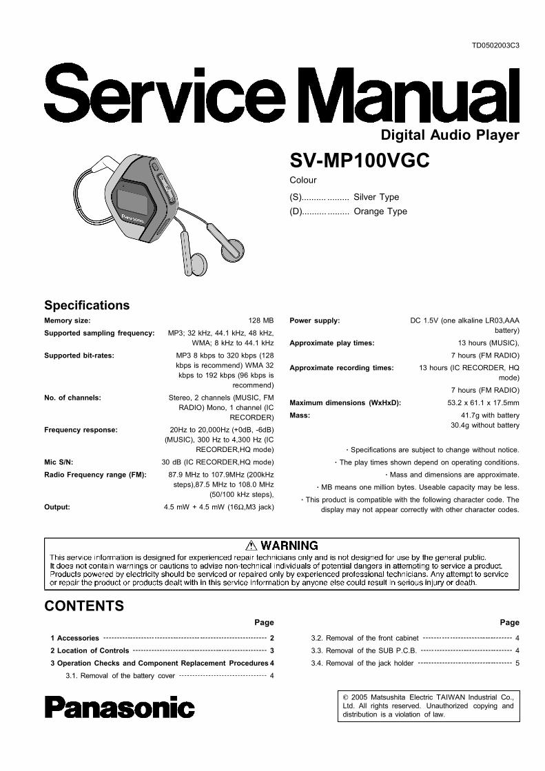
Memory size: 128 MB
Supported sampling frequency: MP3; 32 kHz, 44.1 kHz, 48 kHz,WMA; 8 kHz to 44.1 kHz
Supported bit-rates: MP3 8 kbps to 320 kbps (128kbps is recommend) WMA 32kbps to 192 kbps (96 kbps is
recommend)
No. of channels: Stereo, 2 channels (MUSIC, FMRADIO) Mono, 1 channel (IC
RECORDER)Frequency response: 20Hz to 20,000Hz (+0dB, -6dB)
(MUSIC), 300 Hz to 4,300 Hz (ICRECORDER,HQ mode)
Mic S/N: 30 dB (IC RECORDER,HQ mode)
Radio Frequency range (FM): 87.9 MHz to 107.9MHz (200kHzsteps),87.5 MHz to 108.0 MHz
(50/100 kHz steps),
Output: 4.5 mW + 4.5 mW (16Ω,M3 jack)
1 Accessories 2 2 Location of Controls 3 3 Operation Checks and Component Replacement Procedures 4
3.1. Removal of the battery cover 4
© 2005 Matsushita Electric TAIWAN Industrial Co.,Ltd. All rights reserved. Unauthorized copying anddistribution is a violation of law.
SV-MP100VGCColour
(S).......... ......... Silver Type(D).......... ......... Orange Type
Power supply: DC 1.5V (one alkaline LR03,AAAbattery)
Approximate play times: 13 hours (MUSIC),
7 hours (FM RADIO)Approximate recording times: 13 hours (IC RECORDER, HQ
mode)
7 hours (FM RADIO)
Maximum dimensions (WxHxD): 53.2 x 61.1 x 17.5mm
Mass: 41.7g with battery30.4g without battery
· Specifications are subject to change without notice.
· The play times shown depend on operating conditions. · Mass and dimensions are approximate.
· MB means one million bytes. Useable capacity may be less.
· This product is compatible with the following character code. Thedisplay may not appear correctly with other character codes.
3.2. Removal of the front cabinet 4
3.3. Removal of the SUB P.C.B. 4
3.4. Removal of the jack holder 5
Digital Audio Player
Specifications
CONTENTS Page Page
TD0502003C3

3.5. Removal of the Main P.C.B. 5
3.6. Removal of the LCD Ass馳 5 3.7. Removal of the LCD holder 5
3.8. Removal of the USB cover 6
3.9. Removal of the holder knob 6
3.10. Removal of the REC button and play button and volumebutton and mode button 6
4 Instructions for Repair Service 7 5 Service Position 8 6 Service Mode 9
6.1. Checking Procedures for IC3 C2HBZG000008 9
6.2. Checking Procedures for Font table 10
7 Service Precautions 10
· Stereo earphones
(L0BAB0000193) .................... .................... .................... . 1pc.
· USB Cable
(K1HA05AD0004)............. .................... .................... ........ 1pc.
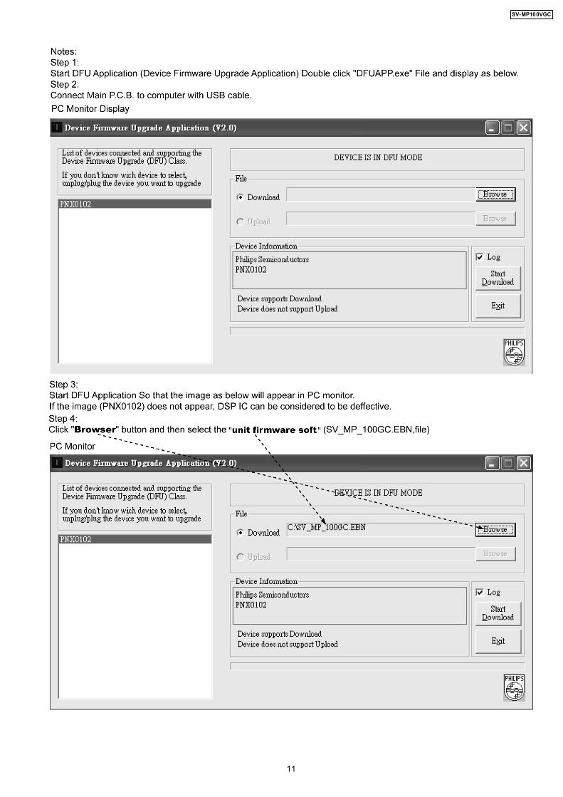
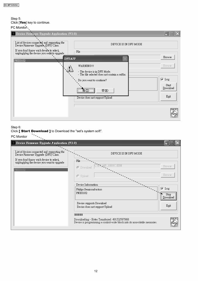
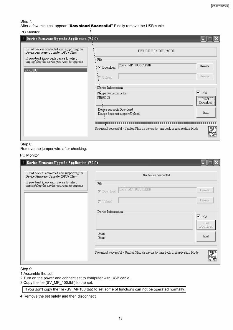
7.1. Install and Copy the software (DFU,firmware,font table)After replacing the main PCB and DSP IC (main
CPU),reinstall DFU and firmware,and copy font table
again. 10
7.2. Please contact to the service organization of the belongingfor the acquisition of data and obtain the software. 10
8 Troubleshooting 14 9 Troubleshooting guide 14 10 Type Illustration of ICs, Transistors and Diodes 15 11 Block Diagram 16 12 Schematic Diagram Notes 21 13 Schematic Diagram 22 14 Printed Circuit Board Diagram 26 15 Cabinet Parts Location 28 16 Packaging 29 17 Replacement Parts List 29
· Neck Strap
(VFC4028) .................... .................... .................... .........1pc.
· CD-ROM Driver
(RFET0002) .................... .................... .................... ........ 1pc.
1 Accessories
2
SV-MP100VGC

2 Location of Controls
REC/STOP
Operation lamp
Microphone
Volume
Turn on, off(Press and hold)/Play/Stop
Battery lid
Earphones jack(3.5 mm stereo)
USB portHOLD switch
Skip/search
Display
(back)
Connection
To USB port
Small end toplayer, largeend to PC
Turn the unit on.(Wait until MODEselect display appears.)
Insert so the arrow isfacing upwards.
1 Press and hold
2
4
3
Connecting to a computer and downloading files
MODE
3
SV-MP100VGC
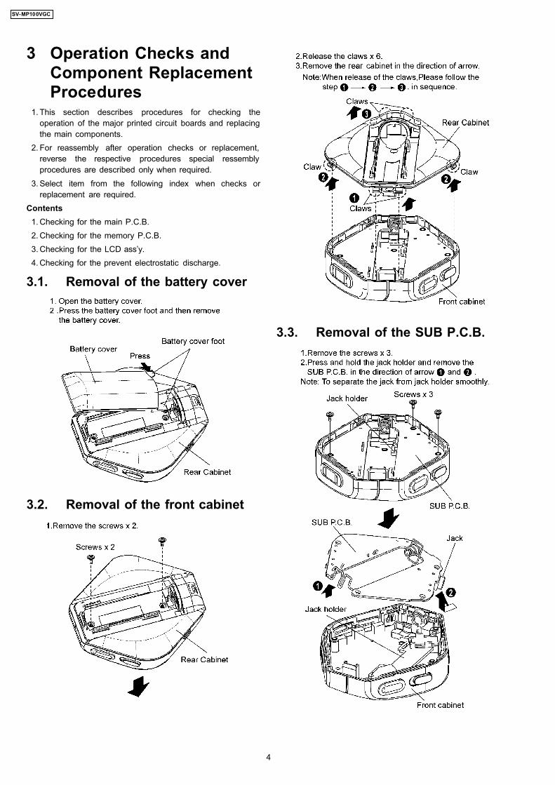
3 Operation Checks andComponent ReplacementProcedures
1. This section describes procedures for checking theoperation of the major printed circuit boards and replacingthe main components.
2. For reassembly after operation checks or replacement,reverse the respective procedures special ressemblyprocedures are described only when required.
3. Select item from the following index when checks orreplacement are required.
Contents 1. Checking for the main P.C.B. 2. Checking for the memory P.C.B. 3. Checking for the LCD ass’y. 4. Checking for the prevent electrostatic discharge.
3.1. Removal of the battery cover
3.2. Removal of the front cabinet
3.3. Removal of the SUB P.C.B.
4
SV-MP100VGC
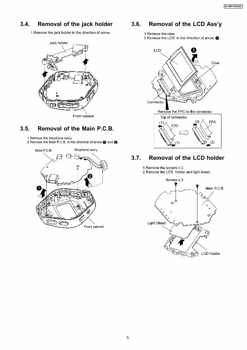
3.4. Removal of the jack holder
3.5. Removal of the Main P.C.B.
3.6. Removal of the LCD Ass’y
3.7. Removal of the LCD holder
5
SV-MP100VGC
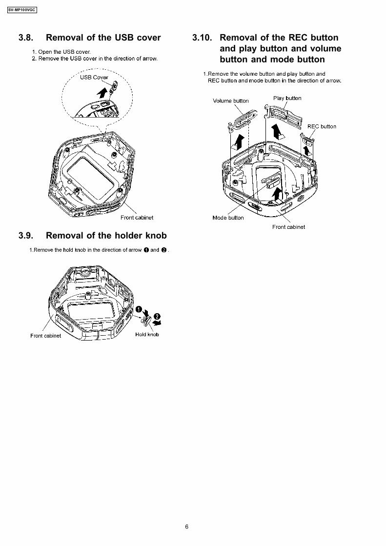
3.8. Removal of the USB cover
3.9. Removal of the holder knob
3.10. Removal of the REC buttonand play button and volumebutton and mode button
6
SV-MP100VGC
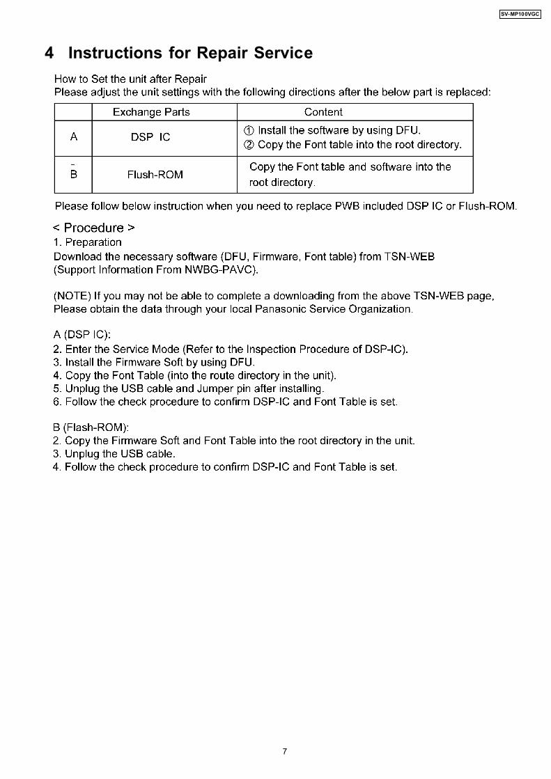
4 Instructions for Repair Service
7
SV-MP100VGC
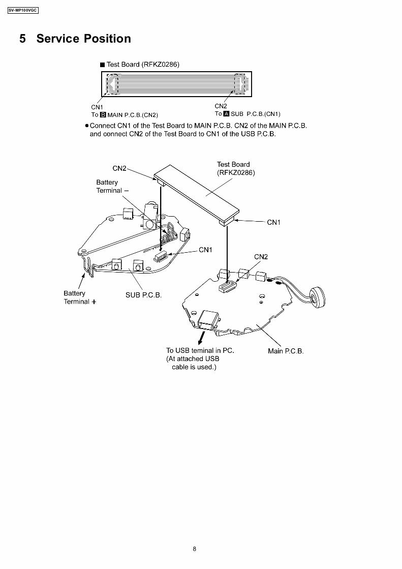
5 Service Position
8
SV-MP100VGC

6 Service Mode6.1. Checking Procedures for IC3 C2HBZG000008
9
SV-MP100VGC

6.2. Checking Procedures for Font table
7 Service Precautions7.1. Install and Copy the software (DFU,firmware,font table) After replacing
the main PCB and DSP IC (main CPU),reinstall DFU and firmware,andcopy font table again.
7.2. Please contact to the service organization of the belonging for theacquisition of data and obtain the software.
10
SV-MP100VGC
11
SV-MP100VGC
12
SV-MP100VGC
13
SV-MP100VGC
8 Troubleshooting · What to prepare
− − − − A PC that has the exclusive application software(Windows Media Player V9.0) installed. Be sure tocheck for normal operation of the PC. If otherapplication software is installed in the PC, be sure thatthis software does not affect the operation of theWindows Media Player V9.0.
− − − − When a user’s product is taken in for service, be sure toobtain not only the player and USB reader/writer . Also,try to obtain as much information as possible on theoperational environmento fthe user’s PC.<PC’s operational environment>Product name, model number, name of CPU, operationclock, RAM capacity, HD capacity, names of installedsoftware, use of USB hub, and any equipmentconnected with USB simultaneous ly.
· Checkpoints before servicing − − − − Does the battery have enough capacity?
Be aware that manganese batteries do not havesufficient capacitor; their use can result in improperoperation.
· Precautions − − − − A PC sometimes does not recognize the USB
reader/writer depending on its conditions (such ascompeting with the installed software). Therefore,always keep the PC in good condition so that anyadaptor can be connected properly.
− − − − There is a possibility that not only the hardware but alsosoftware (PC’s application software) may be the sourceof the problem. Therefore, be sure to inspect allpotential sources carefully and thoroughly beforespecifying any causes.
Remarks: − − − − When the PC does not recognize the USB
reader/writer as a removable disc even when theUSB reader/writer is connected to the PC, this is anindication of an abnormal USB reader/writer . Toconfirm this, and to improve the accuracy of yourservice diagnosis, however, it is recommended thatyou repeat the check procedure with a new, properlyfunctioning USB reader/writer .
− − − − If the PC does not operate normally, it is not possibleto check the problem accurately.
− − − − Be sure to keep the PC working properly accordingto its operating requirements .
− − − − Windows Media Player (V9.0) (recommended) Freedownload from:
http://www.microsoft.com/downloads/
9 Troubleshooting guide · Before repairing the unit, make the below check. · No operation:
− − − − The HOLD function is on. − − − − Replace the battery if it is flat.
· No sound or there is a lot of noise: − − − − Ensure the earphone plug is inserted firmly. − − − − Wipe the plug clean with a clean cloth. − − − − Turn up the volume.
· Play doesn’t resume from the track where I stoppedplay: − − − − This doesn’t work if:
You download, record, or delete files, or change thebattery.The random play mode is on.
· Play doesn’t start from the first track: − − − − The random play mode may be on. − − − − Play usually resumes from the track where you last
stopped play. Use skip to return to the first track. · The unit stops working:
− − − − Take the battery out for about 5 seconds, then reinsertit.
− − − − RESET procedure
1.Slide the HOLD switch to ON.2.Turn the unit on.3.Press [-MODE] 3 times.4.Press [REC/STOP].All the memories in the unit are deleted.
· The display is too dark or too light: − − − − Adjust the contrast.
· Play doesn’t start immediately: − − − − Depending on the amount of data in the unit, it may take
some time for play to start after downloading /recordingor changing the battery.
14
SV-MP100VGC

10 Type Illustration of ICs, Transistors and Diodes
C2HBZG000008C3FBEC000011C1BB0000097
48
E
C
B
46
1
9091
135
136
180
45
No.1
No.1
A
Ca
Anode
Cathode
B0CCAA000001
A
Ca
Anode
Cathode
4
3
5
21
C0DBAGZ0021
43
2
1
C0CBCAC00288 UNR921MJ0LB1ABMB00003
D
G
S
B1CFMC000005
D1
D2
S2
S1
G2
MCH6616
G1
B0JDDB000002
Anode
Cathode
Anode
B0ACEM000008MA2Z74800L
B0ZBZ0000070
ACa
Anode
AAnode
A
Ca
Anode
Cathode
LTSTC170CKTP
15
SV-MP100VGC

11 Block Diagram
Overall Block Diagram
FM Audio
Signal
FM Signal
Rec Signal
IC 1 FM Tuner
IC3 DSP
MP3 Decoder
FM Demodulator
IC Recoder
FM Signal
IC2 Flash memory
12MHz Clock
USB port
Control
Headphone
MIC
DC-DC Conv.
IC 8, 9
Battery
LCD Display
13MHz Clock
Rec Signal
16
SV-MP100VGC
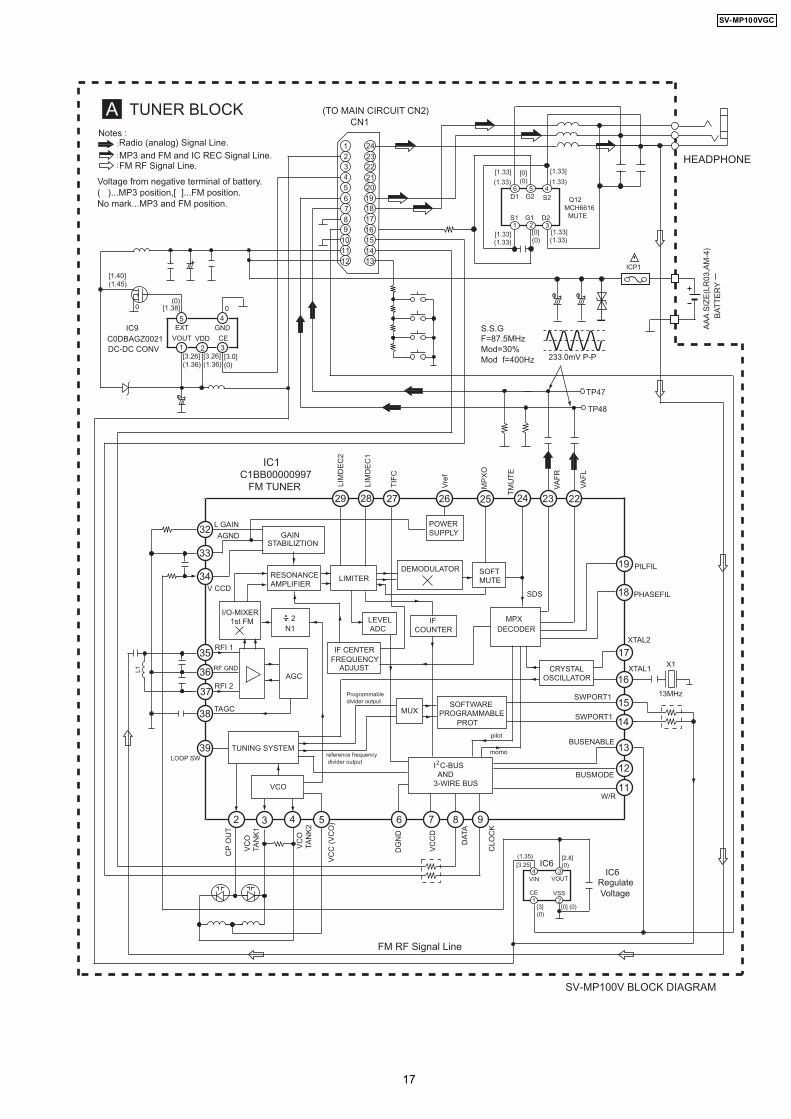
TUNER BLOCKA
IC1
15
14
5
7
9
11
1312
10
8
6
34
12
17
16
1918
2120
2322
24
CN1(TO MAIN CIRCUIT CN2)
HEADPHONE
SV-MP100V BLOCK DIAGRAM
TP48
TP47
S.S.GF=87.5MHzMod=30%Mod f=400Hz 233.0mV P-P
Radio (analog) Signal Line.Notes :
MP3 and FM and IC REC Signal Line.FM RF Signal Line.
Voltage from negative terminal of battery.( )...MP3 position,[ ]...FM position.No mark...MP3 and FM position.
C1BB00000997 FM TUNER
15
14
5 7 9
11
13
12
863 42
17
16
19
18
23 22242829 2627 25
38
39
36
37
34
35
32
33
W/R
L GAIN
AGND
V CCD
RFI 1
RF GND
RFI 2
TAGC
CP
OU
T
VC
OTA
NK
1
VC
OTA
NK
2
VC
C (
VC
O)
DG
ND
VC
CD
DA
TA
CLO
CK
BUSENABLE
BUSMODE
SWPORT1
SWPORT1
XTAL1
XTAL2
LIM
DE
C1
LIM
DE
C2
TIF
C
Vre
f
MP
XO
TM
UT
E
VA
FR
VA
FL
PILFIL
PHASEFIL
GAINSTABILIZTION
RESONANCEAMPLIFIER
LIMITERDEMODULATOR
POWERSUPPLY
SOFTMUTE
MPXDECODER
CRYSTALOSCILLATOR
SOFTWAREPROGRAMMABLE
PROT
I/O-MIXER 1st FM
AGC
N12
TUNING SYSTEM
VCO
IF CENTERFREQUENCY
ADJUST
LEVEL ADC
IFCOUNTER
MUX
Programmable divider output
reference frequency divider output
I C-BUS AND3-WIRE BUS
2
momo
pilot
SDS
X1
13MHz
L1
LOOP SW
FM RF Signal Line
1 2
34VIN VOUT
CE VSS
IC6
[0] (0)
[2.8](0)[3.25]
(1.35)
IC6Regulate Voltage
[3](0)
EXT GND
VOUT VDD CE
5
3
4
1 2
0[1.38]
[3.26](1.36)
[3.26](1.36)
[3.0](0)
(0)0
[1.40](1.45)
AA
AS
IZE
(LR
03
,AM
-4)
BA
TT
ER
Y
ICP1
C0DBAGZ0021DC-DC CONV
IC9
D1 S2
S1 D2G1
G2
[1.33](1.33)
[0](0)
[0](0)
[1.33](1.33)
[1.33]
(1.33)
[1.33]
(1.33)
1 2 3
456
Q12MCH6616 MUTE
17
SV-MP100VGC
SV-MP100V BLOCK DIAGRAM
R18
M16
V10
A17
C9
E18
D16 MPMC address 3
MP
MC
addre
ss 1
6
MP
MC
data
input/outp
ut 0
MP
MC
data
input/outp
ut 4
MP
MC
data
input/outp
ut 3
MP
MC
data
input/outp
ut 2
MP
MC
data
input/outp
ut 1
MP
MC
data
input/outp
ut 5
MP
MC
data
input/outp
ut 7
MP
MC
data
input/outp
ut 6
DA
I S
erial d
ata
input
MPMC_NOE: Output enable for static memories. Active LOW. Used for static memory devices.
MPMC_NSTCS_0: Static memory chip select 0. Default active LOW. Used for static memory device.
U17U14 T17 T15 J17 H15
B14 A13 A1 A2 A3B2 A4 B4 A5 B5 G16
IC3C2HBZG000008
DSP ICA12
A17
C9
E18
D16
A12 MPMC_BLOUT0: The signals nMPMCBLSOUT[0] select byte lane [7:0] on the data bus. Used for static memories.
LCD Display
XATLL_OUT
XTALH_IN
HP_OUTR: SDAC Right Headphone Output
HP_OUTCA: HEADPHONE common output reference
HP_OUTCB: HEADPHONE common output reference
ADC_VINR: SADC Right Analog Input
ADC_VINL: SADC Left Analog Input
LCD_RW-WR: 6800 read/write select 8080 active "high" write enable
LCD_E_RD: 6800 enable 8080 active "high" write enable
LC
D_D
B_4
LC
D_D
B_5
LC
D_D
B-7
LC
D_D
B_6
LC
D_D
B_1
LC
D_D
B-3
LC
D_D
B_2
LCD_RS: 'high' Data register selsct 'low' Instruction register select
LC
D_D
B-0
LCD_CSB: Chip Select
T1
T4
P3
N1
N2
T10
V9
F3 C2B3 C1 C3 D2 D1 D3 E2 E3 F2 G2
HP_OUTL: SDAC Left Headphone Output N3
R3
J1
X2
12MHz
153.3VVDD
D18
ADC_MIC: Microphone Input
USB_DP: Positive USB data line usb 2.0 FS
USB_DM: Negative USB data line usb 2.0 FS
USB_RPU: Soft connect output usb 2.0 FS
USB_VBUS: USB Supply detection line usb 2.0 FS & usb 2.0
USB PORTCN3 3.3V
USB CONTROL
MPMC address 2
A18
MP
MC
_A
_6
MPMC address 5
12 MHz clock input
12 MHz clock input
430.0mV P-P
M17
N17
T18
P17L10
L7DC_DC_LX2: Connection to DC/DC2 external coil
DC_DC_LX1: Connection to DC/DC1 external coil
DC_DC_VBAT: Battery supply voltage
DC_DC_VUSB:USB supply voltage
MP
MC
addre
ss 1
8
IC10Regulator
DC/DC1 3.3V output voltage
DC/DC1 3.3V input voltage
Analog supply 10-bit ADC
976 8 1312 1716 1918
4244 43 41 3637 32 3031 29
N.C R/B RE CE Vcc Vss CLE ALE WE WP
I/O 0
I/O 1
I/O 2
I/O 3
VssVccI/O 4
I/O 5
I/O 6
I/O 7
IC2FLASH MEMORY
B5
A5
B4
A4 A
3
B2
A2
A1
15
14
5
7
9
11
1312
10
8
6
34
12
17
16
1918
2120
2322
24
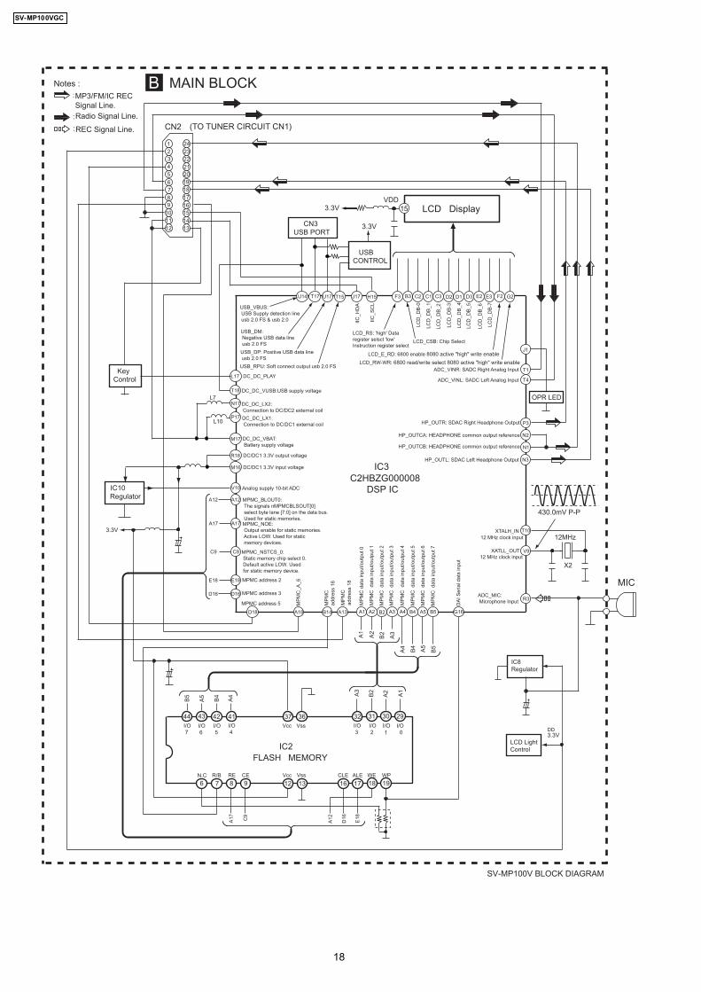
CN2 (TO TUNER CIRCUIT CN1)
L17 DC_DC_PLAY
IIC
_H
DA
IIC
_S
CL
KeyControl
Notes :
REC Signal Line.
Radio Signal Line.
MP3/FM/IC REC Signal Line.
LCD LightControl
IC8Regulator
3.3V
3.3V
A17
C9
E18
D16
A12
A3
B2A2
A1
B5
A5
B4
A4
MIC
OPR LED
DD
MAIN BLOCKB
18
SV-MP100VGC
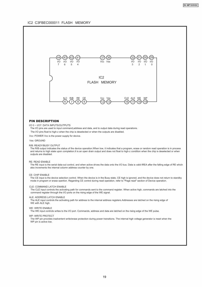
I/O 0 ~ I/O7: DATA INPUTS/OUTPUTS The I/O pins are used to input command,address and data, and to output data during read operations.
The I/O pins float to high-z when the chip is deselected or when the outputs are disabled.
Vcc: POWER Vcc is the power supply for device.
Vss: GROUND
R/B: READY/BUSY OUTPUT The R/B output indicates the status of the device operation.When low, it indicates that a program, erase or random read operation is in process and returns to high state upon completion.It is an open drain output and does not float to high-z condition when the chip is deselected or when outputs are disabled.
RE: READ ENABLE The RE input is the serial data-out control, and when active drives the data onto the I/O bus. Data is valid tREA after the falling edge of RE which also increments the internal column address counter by one.
CE: CHIP ENABLE The CE input is the device selection control. When the device is in the Busy state, CE high is ignored, and the device does not return to standby mode in program or erase opertion. Regarding CE control during read operation, refer to "Page read" section of Device operation.
CLE: COMMAND LATCH ENABLE The CLE input controls the activating path for commands sent to the command register. When active high, commands are latched into the command register through the I/O ports on the rising edge of the WE signal.
ALE: ADDRESS LATCH ENABLE The ALE input controls the activating path for address to the internal address registers.Addresses are latched on the rising edge of WE with ALE high.
WE: WRITE ENABLE The WE input controls writes to the I/O port. Commands, address and data are latched on the rising edge of the WE pulse.
WP: WRITE PROTECT The WP pin provides inadvertent write/erase protection during power transitions. The internal high voltage generator is reset when the WP pin is active low.
PIN DESCRIPTION
976 8 1312 1716 1918
4244 43 41 3637 32 3031 29
N.C R/B RE CE Vcc Vss CLE ALE WE WP
I/O 0
I/O 1
I/O 2
I/O 3
VssVccI/O 4
I/O 5
I/O 6
I/O 7
IC2
FLASH MEMORY
IC2 C3FBEC000011 FLASH MEMORY
19
SV-MP100VGC
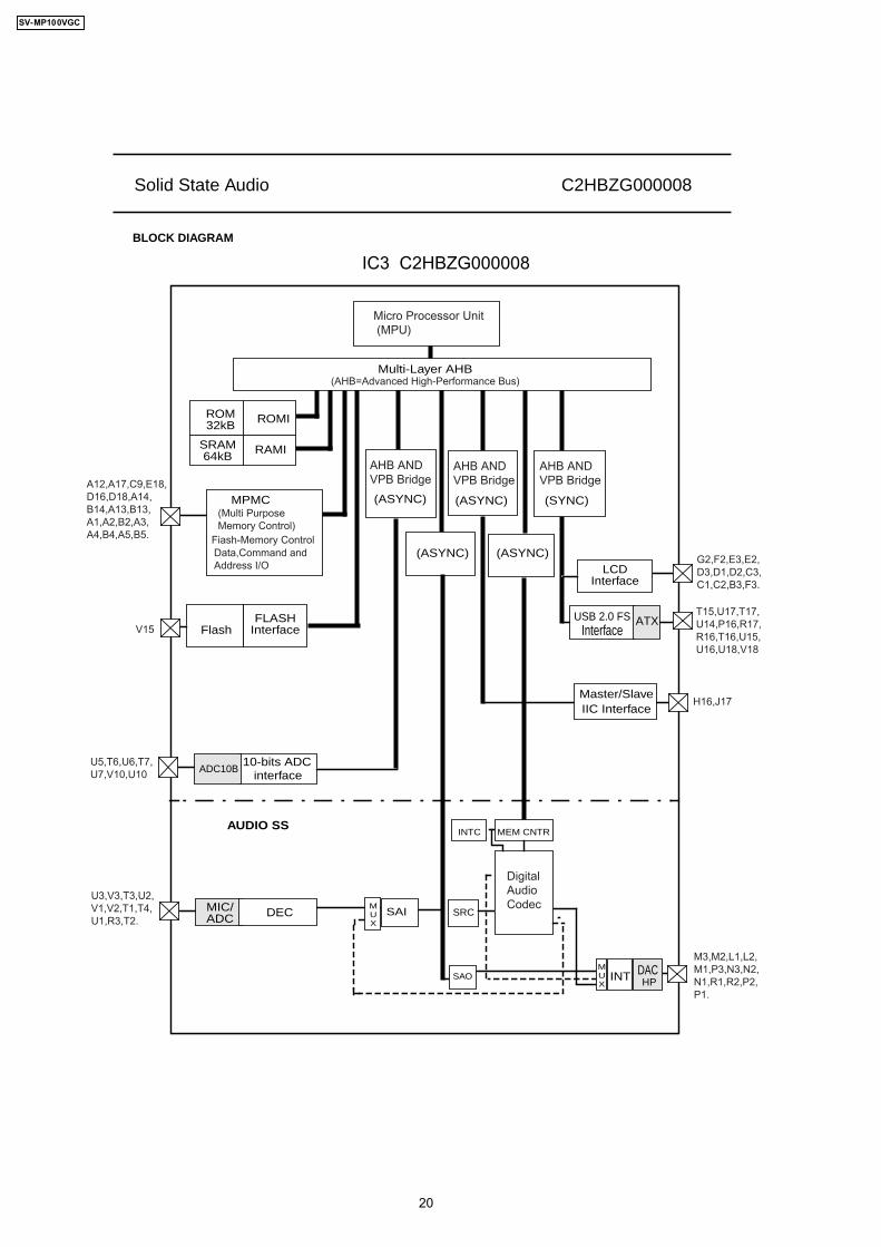
Solid State Audio C2HBZG000008
BLOCK DIAGRAM
LCDInterface
Master/SlaveIIC Interface
SRAM
10-bits ADCinterface
ROM
USB 2.0 FS ATXInterface
FLASHInterfaceFlash
RAMI
ROMI
Multi-Layer AHB
ADC10B
DACINT
32kB
(ASYNC)
(ASYNC)
(ASYNC) (SYNC)
64kB
SAI
SAOHP
MIC/ DECADC
MUX
MUX
SRC
AUDIO SS
(ASYNC)
MEM CNTRINTC
IC3 C2HBZG000008
V15
MPMCA12,A17,C9,E18,D16,D18,A14,B14,A13,B13,A1,A2,B2,A3,A4,B4,A5,B5.
U5,T6,U6,T7,U7,V10,U10
U3,V3,T3,U2,V1,V2,T1,T4,U1,R3,T2.
M3,M2,L1,L2,M1,P3,N3,N2,N1,R1,R2,P2,P1.
H16,J17
T15,U17,T17,U14,P16,R17,R16,T16,U15,U16,U18,V18
G2,F2,E3,E2,D3,D1,D2,C3,C1,C2,B3,F3.
Micro Processor Unit (MPU)
(AHB=Advanced High-Performance Bus)
Digital Audio Codec
(Multi Purpose Memory Control)
Fiash-Memory ControlData,Command and Address I/O
AHB AND VPB Bridge
AHB AND VPB Bridge
AHB AND VPB Bridge
20
SV-MP100VGC

12 Schematic Diagram NotesNotes: · Circuit voltage and waveform described herein shall be
regarded as reference information when probing defectpoint, because it may differ from an actual measuringvalue due to difference of Measuring instrument and itsmeasuring condition and product itself.This schematic diagram may be modified at any timewith the development of new technology.
S1: PLAY / STOP switchS2: FF switchS3: REW switchS4: Volume up switch (VOL +)S5: Volume down switch (VOL -)S6: REC switchS7: MODE switchS8: HOLD switch (HOLD)
· The supply part number is described alone in thereplacement parts list.
· Voltage from negative terminal of battery.
( )...MP3 position, [ ]...FM position.No mark...MP3 AND FM position.
· Voltage and signal line: Positive voltage line: FM RF signal line: Audio signal line: Mp3 signal line: REC signal line
· Important safety notice:
Components identified by mark have specialcharacteristic s important for safety.Furthermore, special parts which have purposes of fire-retardant (resistors), high-quality sound (capacitors), low-noise (resistors), etc. are used.When replacing any of components, be sure to use onlymanufacturers specified parts shown in the parts list.
· Caution!IC and LSI are sensitive to static electricity.Secondary trouble can be prevented by taking care duringrepair.Cover the parts boxes made of plastics with aluminum foil.Ground the soldering iron.Put a conductive mat on the work table.Do not touch the legs of IC or LSI with the fingers directly.
21
SV-MP100VGC
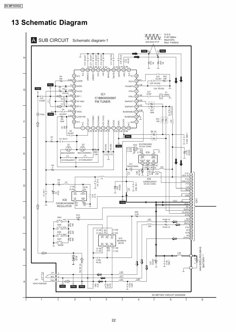
13 Schematic Diagram
C73K100P
IC1C1BB00000997FM TUNER 15
14
5 7 9
11
13
12
10863 41 2
17
16
19
18
21
20
23 222430 2829 2627 25
38
40
39
36
37
34
35
32
33
31
R27100K
TP43
TP66
R6100K
R7
10
K
C8K0.047
R2 0
C3 K0.01R1 0
TP44
TP45
R8 22
R3110K
L5
X1 13MHz
TP47 TP48
C1
9K
0.2
2
C1
8
K0
.22
C1
0
K0
.04
7
C11
K
0.0
47
C1
2
K0
.04
7
C1
3
K0
.03
3
C1
7
K0
.03
3
C23 K0.001
R2233K
C22 K0.022
C24 K0.022
C21D10P
R418K
R5 0 C5
K0.022
L1
C6
J27
PC
7J4
7P
C4
K0.0047
N.C
.
N.C.
N.C.
N.C
.
N.C.N.C
.N
.C. W/R
LGAIN
AGND
VCCD
RFI 1
RF GND
RFI 2
TAGC
LOOP SW
CP
OU
T
VC
OTA
NK
1
VC
OTA
NK
2
VC
C (
VC
O)
DG
ND
VC
CD
DA
TA
CL
OC
K
BUSENABLE
BUSMODE
SWPORT1
SWPORT1
XTAL1
XTAL2L
IMD
EC
1
LIM
DE
C2
TIF
C
Vre
f
MP
XO
TM
UT
E
VA
FR
VA
FL
PILFIL
PHASEFIL
D2D1
B0CCAA000001B0CCAA000001
L3 L4 C14
K0.0
22
C15
K0.0
22
G1C33NJA0037 G1C33NJA0037
L2R310
C1
K0.1
C
24V
22
C9
Z1.0
1 2
34VIN VOUT
CE VSSIC6
C16
Z1.0
A
B
C
D
E
F
G
H
1 2 3 4 5 6
SV-MP100V CIRCUIT DIAGRAM
Schematic diagram-1
R891.5K
TP55
SUB CIRCUIT A
20
2
1
3
4
5
6
7
8
9
10
11
12
13
14
15
16
17
18
19
24
21
22
23
AA
AS
IZE
(LR
03
,AM
-4)
BA
TT
ER
Y
CN
1
C27
4V
220
C12DD3.3V
F16VDD-CE
F17
Lch
Rch
USB
VCC
VCC
AD
DATA
CLOCK
G3(Lch)
(Rch)
F18C6
G18
H3(Com)
L4
4
EXT GND
VOUT VDD CE
5
3
4
1 2
C
92
4V
100
Q10 B1CFMC0005
IC9
C0DBAGZ0021
C93
4V
220
C98 K
0.1
R13 6.8KSW4
SW5VOL
R14
10K
VOL +
SW6REC
R1
52
2K
R1
66
8KSW7
MODE
D11MA2Z74800L
L37
L91
D1 S2
S1 D2G1
G2
[1.33](1.33)
[0](0)
[0](0)
[1.33]
(1.33)
[1.33]
(1.33)
[1.33]
(1.33)
1
2
3
JK1
K2HC103E0026
L51
L52
L50
L64
C1
05
10
0P
TP53
FM
R
F_
IN
TP52TP54
D1
9
Lch
Rch
Com
1 2 3
456
C8
00
.22
C8
20
.22
C106K0.22
A18
0.690.701.441.521.41.881.88
0
2.98
0.02
0.02
1.62
1.35
0.5
0.58 2.59 2.59 2.59 0 2.59 2.96 2.96
0.54
0
2.59
1.05
0
1.05
0.81
2.57
TP42
TP46
Q12MCH6616 MUTE
[3](0)
[0](0)
[2.8](0)[3.25]
(1.35)
C0CBCAC00288REGULATOR
0[1.38]
[3.26](1.36)
[3.26](1.36)
[3.0](0)
(0)0
[1.40](1.45)
DC-DC CONV
IC9
DC-DC CONV
S.S.GF=87.5MHzMod=30%Mod f=400Hz233.0mV P-P
R923.3K
C1
23
0
.1
L62
L65
L69
L92
C127
KB
0.1
C126 K
B0.1
C125
4V
220
L90
C1
30
KB
0.1
R108 10
R109 10
R2
91
M
R1
91
M
22
SV-MP100VGC
7 8 9 10 11
:POSITIVE VOLTAGE LINE :AUDIO(DIGITAL) SIGNAL LINE :AUDIO(ANALOG) SIGNAL LINE
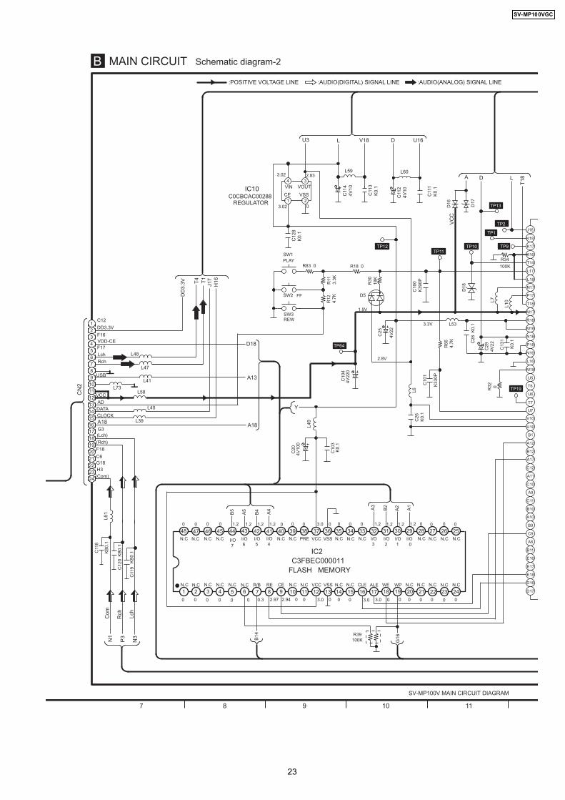
SV-MP100V MAIN CIRCUIT DIAGRAM
L47
20
2
1
3
4
5
6
7
8
9
10
11
12
13
14
15
16
17
18
19
24
21
22
23
CN
2
J16
K18
K16
T14
L17
L18
N17
P17
T18
K17
M17
R18
M16
N18
P18
N16
L16
M18
U5
T6
U6
T7
U7
V10
U10
B1
A12
B12
A17
C12
A11
C10
A9
C11
B10
A10
B9
C9
A8
B11
E16
E17
E18
D16
D171 2 119753 4 6 8 10 1312 1514 1716 1918 2120 2322 24
48 47 3840424446 45 43 41 39 3637 3435 3233 3031 2829 2627 25
N.C N.C N.C N.C N.C N.C R/B RE CE VCCN.C N.C VSS CLEN.C N.C ALE WE WP N.C N.C N.C N.C N.C
N.CN.CN.CN.CI/O 0
I/O 1
I/O 2
I/O 3
N.CN.CN.CVSSVCCPREN.CN.CI/O 4
I/O 5
I/O 6
I/O 7
N.CN.CN.CN.C
IC2C3FBEC000011
FLASH MEMORY
0 0 0 0 0 0 0.3 2.97 2.94 0 0 3.0 0 0 0 3.0 3.0 0 0 0 0 0 0 0
0 01.2 0 01.21.21.20 00 03.01.21.21.21.2 0 000 000
Schematic diagram-2MAIN CIRCUIT B
L48
L41
L73L58
L40
L39
L7
L10
TP19R3
2
0
C2
94
V2
2C2
8
K0
.1L53
R34
100K
TP13
TP2
TP1
TP9TP10
D1
8
TP11TP12
C1
00
K3
90
P
R18 0
R3
01
8K
D5
1.5V
3.3V
R6
64
.7K
C1
01
K3
30
P
L6
C2
6K
0.1
C2
5
4V
22
SW1
SW2
SW3
PLAY
FF
REW
R83 0
R11
3.3
KR
12
4.7
K
L61
C11
8
KB
0.1
C1
20
KB
0.1
C11
9K
B0
.1
VIN
1 2
34
IC10 VOUT
CE VSS
L59 L60
C11
44V
10
C11
3K
0.1
C11
24V
10
C11
1K
0.1
L49
C2
04
V1
00
C1
03
K0
.1
2.8V
TP64
R39100K
C12
DD3.3V
G3
VDD-CEF17
Lch
Rch
USB
VCC
AD
DATA
CLOCK
F16
(Lch)
(Rch)
F18
C6G18
H3
(Com)
A18
D18
A18
LU3 V18 D U16
D L
T18
DD
3.3
V T4 T1
J17
H1
6
A13
Y
Lch
Rch
Com
G16
B14
B5
A5
B4
A4 A
3
B2
A2
A1
VC
CD
16
A
D1
7
C0CBCAC00288REGULATOR
3.02
3.02 2.83
0
N1
P3
N3
C1
04
4V
22
0
C1
31
K0
.1
C128
K0.1
23
SV-MP100VGC

D18
J16
K18
K16
T14
L17
L18
N17
P17
T18
K17
M17
R18
M16
N18
P18
N16
L16
M18
U5
T6
U6
T7
U7
V10
U10
B1
A12
B12
A17
C12
A11
C10
A9
C11
B10
A10
B9
C9
A8
B11
E16
E17
E18
D16
D17
A18
V18 U18
MP
MC
_A
_5
MPMC_A_4MPMC_A_3MPMC_A_2MPMC_A_1
MP
MC
_A
_9
MP
MC
_A
_8
MP
MC
_A
_7
MP
MC
_A
_6
MP
MC
_A
_13
MP
MC
_A
_12
MP
MC
_A
_11
MP
MC
_A
_10
MP
MC
_A
_15
MP
MC
_A
_14
MP
MC
_A
_19
MP
MC
_A
_18
MP
MC
_A
_17
MP
MC
_A
_16
MP
MC
_D
_0
MP
MC
_A
_20
MP
MC
_D
_4
MP
MC
_D
_3
MP
MC
_D
_2
MP
MC
_D
_1
MP
MC
_D
_5
MP
MC
_D
_9
MP
MC
_D
_8
MP
MC
_D
_7
MP
MC
_D
_6
MP
MC
_D
_10
MP
MC
_D
_14
MP
MC
_D
_13
MP
MC
_D
_12
MP
MC
_D
_11
MP
MC
_D
_15
DA
O_C
LK
DA
I_D
ATA
DA
I_W
S
DA
I_B
CK
DA
O_D
ATA
DA
O_W
S
DA
O_B
CK
JTA
G_T
RS
T_N
JTA
G_T
CK
JTA
G_T
DI
JTA
G_T
D0
JTA
G_T
MS
JTA
G_S
EL
AR
M
XTALL_GNDAXTALL_OUT
XTALL_VDDA18XTALL_IN
XTALL_VSSA
SPDIF_GNDA
XATLL_OUT
XTALH_VDDA18
XTALH_IN
SPDIF_VDDA33
SPDIF_IN
HP_OUTR
HP_OUTCA
HP_OUTCB
HP_OUTL
HP_VDDA33A
HP_VDDA33B
HP_GNDAA
HP_GNDAB
DAC_VOUTR
DAC_VOUTL
DAC_VDDA33
DAC_VREEP
DAC_VREFN
ADC_VREFN
ADC_GNDA
ADC_VINR
ADC_VINL
ADC_VREF
ADC_MIC
ADC_MIC_LNA
ADC_VDDA33
ADC_VDDA18
ADC_VCOM
ADC_VREFP
GPIO_UART_1
GPIO_UART_0
GPIO_UART_2
GPIO_UART_3GPIO_MIC_0
GPIO_MIC_1
GPIO_MIC_3
GPIO_MIC_4
GPIO_MIC_5
GPIO_MIC_2
LC
D_R
W-W
R
LC
D_E
_R
D
LC
D_D
B_4
LC
D_D
B_5
LC
D_D
B-7
LC
D_D
B_6
LC
D_D
B_1
LC
D_D
B-3
LC
D_D
B_2
LC
D_R
S
LC
D_D
B-0
LC
D_C
SB
VD
DE
6
VD
DE
5
VS
SE
4
VS
SE
1
VD
DE
4
VD
DE
3
VD
DE
2
VD
DE
1
VS
SE
6
VS
SE
5
VS
SE
4
VS
SE
3
VS
SI3
VS
SI2
VS
SI1
VD
DI3
VD
DI2
VD
DI1
FLA
SH
_V
DD
_H
V
IIC
_S
DA
IIC
_S
CL
US
B_D
P
US
B_D
M
US
B_R
PU
US
B_G
ND
A
US
B_V
BU
S
US
B_R
RE
F
US
B_V
DD
A18_B
G
US
B_V
DD
A18_P
LL
US
B_V
SS
A_T
EE
M
US
B_V
SS
A_R
EF
US
B_V
DD
A33
US
B_V
DD
A33-D
RV
GPIO_3GPIO_2
GPIO_1GPIO_0RSTIN_N
DC_DC_PLAY
DC_DC_STOP
DC_DC_LX2
DC_DC_LX1
DC_DC_VUSB
DC_DC_VBAT
DC_DC_VOUT33A
DC_DC_VOUT33B
DC_DC_VOUT18
DC_DC_VSS1
DC_DC_VSS2
DC_DC_GND
DC_DC_CLEAN
ADC10B_GPA4
ADC10B_GPA3
ADC10B_GPA2
ADC10B_GPA1
ADC10B_GPA0
ADC10B_VDDA33
ADC10B_GMDA
MPMC_RPOUT
MPMC_BLOUT0
MPMC_BOUT1
MPMC_NOE
MPMC_DQM_0
MPMC_DQM_1
MPMC_NCAS
MPMC_NRAS
MPMC_NWE
MPMC_CKE
MPMC_CLKOUT
MPMC_NDYCS
MPMC_NSTCS_0
MPMC_NSTCS_1
MPMC_NSTCS_2
MPMC_A_0
K1
K2
L3
H2
G3
H3
J2
J1
J3
K3
U3
V3
T3
U2
V1
V2
T1
T4
U1
R3
T2
M3
M2
L1
L2
M1
P3
N2
N1
N3
R1
R2
P2
P1
T12
U11
T11
T10
U9
V9
T9
V7
U8
T8
V8
U16
V18 U16
U15 T16 R16 R17 P16 U14 T17 U17 H16T15 J17 V15 G1V17 V12 V16 V11 H1 A6 A15 A7 A16 H18 V6V13 F1 J18 V14 V5 E1 F3
H18
C2B3 C1 C3 D2 D1 D3 E2 E3 F2 G2
F18G18 F17 T13 V4 U12 T5 U13 U4C18B18 B17 C17 B16 C16 B15 C15 A14 C14B14 A13 B13 C13 A1 A2 A3B2 A4 B4 A5 B5 C4 C5 B6C6 C7 B7 B8C8 H17 G17 F16G16
IC3
C2HBZG000008
CN3 USB CON.
ID +D
AT
A
GN
D
DA
TA
Vb
us
K1FB105E0004
245 3 1
R37 0
C30
K0.01
R38 1
M
R102 1
.5K
1.8
VL11
L12
L13 L
14 L15
L16
C31 K
0.1
C33 K
0.1
L57
C109 K
0.1
R41
R4010K C
32
K0.1 TP5
TP4
TP7
TP6 TP8
R43
100K
TP3
13 14 15 16 17 18
SV-MP100V CIRCUIT DIAGRAM
B5
A5
B4
A4
A1
G16B2
A2
A3
B14
Y
A13
T18
LD
LD
A B C D E F G H I J K L
H17
A14 100K
DSP MICON IC
C6
Schematic diagram-3MAIN CIRCUIT B
12K
C88
C91
K0.0
1R
36
1K
C87
6P
R101180K
R90 0
6P
R68
R103 100K
D18
A18
H16J17
ONSW8HOLD
OFF
A
C128 K
0.1
24
SV-MP100VGC

12
11
9
7
5
34
6
8
10
1312
1514
1716
19
18
2120
2322
24
30
2829
2627
25
CN4LCD CON.
K1MN30B00124
K1
K2
L3
H2
G3
H3
J2
J1
J3
K3
U3
V3
T3
U2
V1
V2
T1
T4
U1
R3
T2
M3
M2
L1
L2
M1
P3
N2
N1
N3
R1
R2
P2
P1
T12
U11
T11
T10
U9
V9
T9
V7
U8
T8
V8
C39
K0.1
C51
4V
68
2.8VL21
L19
L25
C49
4V
220
C40
K0.1 R51
10
C43
K0.1
C48
Z1.0
C50
K0.1
L22R53 10
L24R54150
C52
4V
220
C53
4V
220
C44
K0.1
C45
K0.1
C36
K0.1
C38
6.3
V10
L18
C35
K0.1
L23
L20
C46
K0.1
C55
4V
22
C86 K
0.1
C42
K0.1
C37
J18P
X2 12MHz
C41
J18P
R55 4.7
K
R65
330K
C57 Z1.0
C90 Z1.0
C58 Z1.0
C59 Z1.0
C60 K0.1
C61 K0.1C62 K0.1
C63 K0.1C64 K0.1
NC/CS1
/RESA0WR (R/W)RD(E)DB0DB1DB2DB3
DB4DB5DB6DB7VDDVSSVOUTCAP3+CAP1-CAP1+
CAP2-CAP2+V0
V1V2
V3V4C86P/SNC
D3 E2 E3 F2 G2
V4 U12 T5 U13 U4
19 20 21 22 23 24
SV-MP100V CIRCUIT DIAGRAM
A
B
C
D
E
F
G
H
D
T4
A
B
CDEFGHIJ
K
L
P3
A14
T1
R73
357K
C96 K
0.1
430.0mV P-P
MIC
1 2
34VIN VOUT
CE VSS
IC8
C72
K0.0
47C68
390P
R582.2K
C
70
4V
100
R57 1K
C107 4V
100
C67
180P
MIC-INPUT
R105 330K
R106 10K
C11
54V
10
C11
6 0.1
R104 10K
Schematic diagram-4MAIN CIRCUIT B
D10 R62 1.5K
R74 15
D12
Q11B1ABMB00003BACK LIGHT
R76 1K
DD 3.3V
TP50
TP51
1.8V
U32.8V
LL42R78 2.7K
3.3V
DD 3.3V
R43
100K
TP3
Rch
N1Com
N3Lch
H17
C0CBCAC00288REGULATOR
[3.26](1.36)
[0](0)
[2.82](1.36)
[3.26](1.36)
0.18V0.75V
0V
25
SV-MP100VGC

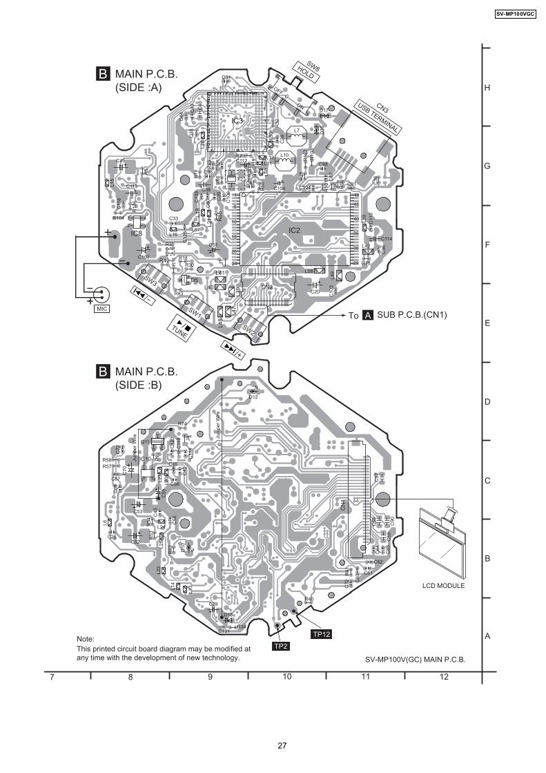
14 Printed Circuit Board Diagram
A
B
C
D
E
F
G
H
654321
Note: This printed circuit board diagram may be modified atany time with the development of new technology. SV-MP100V(GC) MAIN P.C.B.
C98
L44
R7
R14
L4
C7
C6
R4 R5
C10
D1
R1
R22
C73
C11
1 2
34
C5
C3
C4
R92
C130
CN1
SUB P.C.B. (SIDE :A)
A
SUB P.C.B. (SIDE :B)
A
C14R2
C15
L3
L2
R3
L5
R27
R8
R31
C16
C9
C1
C2
X1
C23
C24
C22 C19
C17
C82
L1
R6
C8
C13
C12
C18C21
IC6
IC1
D2
L51
L50
L52
SD
G
To MAIN P.C.B. (CN2)CB
15
5
11
10 1
21
20
3025
40
35
31
R89
C27
C93C92
C127
R16
C80
Q12
1234
56
IC9
D11
1234
5
Q10 C106
L37JK1
R15
R13
1AAA SIZE(LR03,AM-4)BATTERY 1.5V
SW7
MODE
SW6
REC/STOP
SW5
VOL
SW4VOL +
HEADPHONE
JACK
C123
L64 C105
R29 R19
J1
L91
L92
L62
R108
L65
R109
L69
J3 J2
L90
ANT Wire
ANT Wire
ICP1
C126
C125
26
SV-MP100VGC
B
C
D
E
F
G
H
A
127 8 9 10 11
Note: This printed circuit board diagram may be modified atany time with the development of new technology. SV-MP100V(GC) MAIN P.C.B.
D17
D16R
32
C28
L7
L53
L10
C36
MIC
C103
L41
L47
L48
C88
C20
R90C
87
C91
C11
3
D5
C35
C44
R39
C43
R11
L59
R101
R68
R102
R103
R38R
51
C49
C107R12
R18
R30
R83 L39L40 CN2
C33
L16
R104
C11
6
R106
L15
L57
C115C38
C51
L21
L19
R65
C109
C40 C
39
C100
R19
R66
R43
C101
C36 C37
R55C41
C11
1
R29C112
L12L11
L60
X2
IC3
IC2
L18
C48
C31
L58
L49
C96
R78
L42
C114IC8
1
2 3
4
LCD MODULE
C26C52
L6
C53
L14
L22
L25
L24
R53
R54
C45
C68
C67
R58R57
C72
C70
IC10
L23
L20
R76
Q11
C29
R74
C86
C46
C42
C55
C50
R62
R34
D18
D12
D10
E
C
B
12
3 4
R40
C57
C58
C59
C90
C62
C63
C64
C60 C61R
41
C32
CN
4
L13
MAIN P.C.B. (SIDE :B)
B
MAIN P.C.B. (SIDE :A)
B
To SUB P.C.B.(CN1)A
1
5
10
15
20
24 25
30
35
40
45
48
SW8HOLD
ON
OFFC
CN3USB TERMINAL
SW3
SW1
SW2
/
/+
TUNE
/
C104
J1
C124J4
C11
9C
120
C11
8
C131
TP2
TP12
C128
Jum
per
Wire
Jum
per
Wire
27
SV-MP100VGC

15 Cabinet Parts Location
28
SV-MP100VGC

17 Replacement Parts ListNotes:
· Important safety notice:
Components identified by mark have specialcharacteristic s important for safety.Furthermore, special parts which have purposes of fire-retardant (resistors), high-quality sound (capacitors),low-noise (resistors), etc. are used.When replacing any of components, be sure to use onlymanufactures specified parts shown in the parts list.
1. (T) Indicates parts that are supplied TAMACO 2. The reference number SA represent the grease tool
usea for unit.
3. The marking (RTL) indicates that Retention Time isLimited for this item. After the discontinuation of thisassembly in production, the item will continue to beavailable for a specific period of time. The retentionperiod of availability is dependent on the type ofassembly, and in accordance with the laws governingpart and product retention. After the end of this period,the assembly will no longer be available.
Ref. No. Part No. Part Name & Description Remarks
CABINET PARTS
K1 RFKKVMP100VS UP CHASSIS ASSEMBLY(Silver)
(T)
K1 RFKKVMP100VD UP CHASSIS ASSEMBLY(Orange)
(T)
K2 RKST0103-S REAR CABINET (T)
K3 RKKT0059-S BATTERY COVER (T)
K4 RGUT0210-H REC BUTTON (Silver) (T)
K4 RGUT0210-D REC BUTTON (Orange) (T)
16 Packaging
29
SV-MP100VGC

Ref. No. Part No. Part Name & Description Remarks
K5 RGVT0093-S HOLD KNOB (T)
K6 RGUT0213-S MODE BUTTON (T)
K7 RGUT0212-H VOL BUTTON (Silver) (T)
K7 RGUT0212-D VOL BUTTON (Orange) (T)
K8 RGUT0211-S PLAY BUTTON (T)
K9 RGQT0051-H USB COVER (T)
K10 ZA3MP100V MIC ASSEMBLY (T)
K10-1 RMGT0067 MIC GUM (T)
K10-2 AC1033UL2728 MICROPHONE (T)
K11 ZA2MP100V LCD ASSEMBLY (T)
K11-1 RKWT0108-Q LED PANEL (T)
K11-2 RMNT0101 LCD HOLDER (T)
K11-3 RGCT0011-Q LGP (T)
K11-4 L5DCBDB00003 LCD WITH FPC (30 Pin) (T)
K12 RMZT0084 SHIELD SHEET (T)
K13 RGNT0251 NAME PLATE (T)
K14 RJCT40016 BATTERY TERMINAL TOUCH (T)
K15 RJCT80013 BATTERY TERMINAL TOUCH (T)
K16 RHQT0022-S SCREW (T)
K17 RMNT0102 JACK HOLDER (T)
K18 RHQT0017 SCREW (T)
K19 XTNR14+45CFZ PCB SCREW (T)
K20 RMZT0085 SHIELD SHEET (T)
ACCESSORIES
A1 L0BAB0000193 INNERPHONE (T)
A2 RFET0002 USB2.0 DRIVER DISC PIECE (T)
A3 K1HA05AD0004 USB CABLE (T)
A4 VFC4028 NACK STRAP (T)
A5 RQTT0665-G INSTRUCTION BOOK (T)
A6 RQTT0666-K INSTRUCTION BOOK (T)
A7 RQTT0667-R INSTRUCTION BOOK (T)
A8 RQTT0719-R INSTRUCTION BOOK (T)
PACKING MATERIALS
P1 RPKT0753-1 DECORATION BOX (Silver) (T)
P1 RPKT0754-1 DECORATION BOX (Orange) (T)
P1 RPKT0757-1 DECORATION BOX (Silver) (T)
P1 RPKT0758-1 DECORATION BOX (Orange) (T)
P2 RPNT0523 PAD(FIXTURE) (T)
P.C.B.
PCB1 P1MP100VGC MAIN BOARD ASSEMBLY (T)
PCB2 P2MP100VGC SUB BOARD ASSEMBLY (T)
PCB3 RFKZ0286 TEST BOARD (T)
INTEGRATED CIRCUITS TRANSISTORS AND DIODES
IC1 C1BB00000997 FM TUNER IC (40 PIN) (T)
IC2 C3FBTC000023 128MB FLASH MEMORY (T)
IC3 C2HBZG000008 DSP IC(BGA 180 PIN) (T)
IC6 C0CBCAC00288 IC (T)
IC8 C0CBCAC00288 IC (T)
IC9 C0DBAGZ00021 DC/DC IC(D5P) (T)
IC10 C0CBCAC00288 IC (T)
Q10 B1CFMC000005 FET (T)
Q11 B1ABMB000003 TRANSISTOR (T)
Q12 SSM6N25TU FET (T)
D1 B0CCAA000001 LOW-VOLTAGE VARIABLE CAP (T)
D2 B0CCAA000001 LOW-VOLTAGE VARIABLE CAP (T)
D5 B0JDDB000002 DIODE (T)
D10 LTSTC170CKTP CHIP L.E.D.(RED) (T)
D11 MA2Z74800L DIODE (T)
D12 B3AFB0000090 CHIP.LED. (T)
D13 B0ZBZ0000070 Varistor C.V.19V (T)
D16 B0ZBZ0000070 Varistor C.V.19V (T)
D17 B0ZBZ0000070 Varistor C.V.19V (T)
D18 B0ZBZ0000070 Varistor C.V.19V (T)
COILS AND TRANSFORMERS
L1 G1CR12JA0037 CHIP INDUCTOR (T)
L2 J0JBC0000044 CHIP COIL (T)
L3 G1C33NJA0037 CHIP INDUCTOR (T)
L4 G1C33NJA0037 CHIP INDUCTOR (T)
L5 J0JBC0000044 CHIP COIL (T)
L6 J0JBC0000044 CHIP COIL (T)
L7 G1A220C00006 POWER INDUCTOR (T)
L10 G1A220C00006 POWER INDUCTOR (T)
L11 J0JBC0000044 CHIP COIL (T)
L12 J0JBC0000044 CHIP COIL (T)
Ref. No. Part No. Part Name & Description Remarks
L13 J0JBC0000044 CHIP COIL (T)
L14 J0JBC0000044 CHIP COIL (T)
L15 J0JBC0000044 CHIP COIL (T)
L16 J0JBC0000044 CHIP COIL (T)
L18 J0JBC0000044 CHIP COIL (T)
L19 J0JBC0000044 CHIP COIL (T)
L20 J0JBC0000044 CHIP COIL (T)
L21 J0JBC0000044 CHIP COIL (T)
L22 J0JBC0000044 CHIP COIL (T)
L23 J0JBC0000044 CHIP COIL (T)
L24 J0JBC0000044 CHIP COIL (T)
L25 J0JBC0000044 CHIP COIL (T)
L37 G1A220C00006 POWER INDUCTOR (T)
L39 BK1608HS102 FERRITE BEAD (T)
L40 BK1608HS102 FERRITE BEAD (T)
L41 BK1608HS102 FERRITE BEAD (T)
L42 J0JGC0000021 FERRITE BEAD (T)
L44 BK1608HS102 FERRITE BEAD (T)
L47 BK1608HS102 FERRITE BEAD (T)
L48 BK1608HS102 FERRITE BEAD (T)
L49 BK1608HS102 FERRITE BEAD (T)
L50 J0JCC0000077 CHIP COIL (T)
L51 J0JCC0000077 CHIP COIL (T)
L52 J0JCC0000077 CHIP COIL (T)
L53 J0JBC0000044 CHIP COIL (T)
L57 J0JBC0000044 CHIP COIL (T)
L58 J0JGC0000021 FERRITE BEAD (T)
L59 J0JBC0000044 CHIP COIL (T)
L60 J0JBC0000044 CHIP COIL (T)
L62 BK1608HS102 FERRITE BEAD (T)
L64 BK1608HS102 FERRITE BEAD (T)
L65 BK1608HS103 FERRITE BEAD (T)
L69 J0JGC0000021 FERRITE BEAD (T)
L91 J0JGC0000021 FERRITE BEAD (T)
L92 BK1608HS102 FERRITE BEAD (T)
L93 RLL300040-Y CHOCK COIL (T)
SWITCHES
SW1 K0H1BB000068 SWITCH (T)
SW2 K0H1BB000068 SWITCH (T)
SW3 K0H1BB000068 SWITCH (T)
SW4 K0H1BB000068 SWITCH (T)
SW5 K0H1BB000068 SWITCH (T)
SW6 K0H1BB000068 SWITCH (T)
SW7 K0H1BB000068 SWITCH (T)
SW8 K0D112B00071 SLIDE SWITCH (T)
JACK
JK1 K2HC103E0026 M3.5 JACK GARY (T)
CRYSTAL
X1 H0J480500015 CRYSTAL(13MHZ) (T)
X2 H0J120500034 CRYSTAL 12MHz (T)
SOCKET
CN1 K1KB24A00045 24 PIN CONNECTOR (HEADER) (T)
CN2 K1KB24A00044 24 PIN CONNECTOR (SOCKET) (T)
CN3 K1FB105E0004 USB SOCKET (T)
CN4 K1MN30B00124 LCD FPC CONNECTOR (30 PIN (T)
CHIP JUMPERS
ICP1 D0GBR00JA008 CHIP RESISTOR (T)
RESISTORS
R1 D0GAR00JA020 CHIP RESISTOR (T)
R2 D0GAR00JA020 CHIP RESISTOR (T)
R3 D0GA100JA020 CHIP RESISTOR (T)
R4 D0GA183JA020 CHIP RESISTOR (T)
R5 D0GAR00JA020 CHIP RESISTOR (T)
R6 D0GA104JA020 CHIP RESISTOR (T)
R7 D0GA103JA020 CHIP RESISTOR (T)
R8 D1H42202A014 CHIP RESISTOR (T)
R11 D0GA332JA020 CHIP RESISTOR (T)
R12 D0GA472JA020 CHIP RESISTOR (T)
R13 D0GA682JA020 CHIP RESISTOR (T)
R14 D0GA103JA020 CHIP RESISTOR (T)
R15 D0GA223JA020 CHIP RESISTOR (T)
R16 D0GA683JA020 CHIP RESISTOR (T)
R18 D0GAR00JA020 CHIP RESISTOR (T)
R19 D0GA105JA020 CHIP RESISTOR (T)
30
SV-MP100VGC

Ref. No. Part No. Part Name & Description Remarks
R22 D0GA333JA020 CHIP RESISTOR (T)
R27 D1H41042A014 CHIP RESISTOR (T)
R29 D0GA105JA020 CHIP RESISTOR (T)
R30 D0GA183JA020 CHIP RESISTOR (T)
R31 D1H41032A014 CHIP RESISTOR (T)
R32 D0GAR00JA020 CHIP RESISTOR (T)
R34 D0GA104JA020 CHIP RESISTOR (T)
R36 D0GA102JA020 CHIP RESISTOR (T)
R38 D0GA105JA020 CHIP RESISTOR (T)
R39 D1H41042A014 CHIP RESISTOR (T)
R40 D0GA103JA020 CHIP RESISTOR (T)
R41 D0GA104JA020 CHIP RESISTOR (T)
R43 D0GA104JA020 CHIP RESISTOR (T)
R51 D0GA100JA020 CHIP RESISTOR (T)
R53 D0GA100JA020 CHIP RESISTOR (T)
R54 D0GA151JA020 CHIP RESISTOR (T)
R55 D0GA472JA020 CHIP RESISTOR (T)
R57 D0GA102JA020 CHIP RESISTOR (T)
R58 D0GA222JA020 CHIP RESISTOR (T)
R62 D0GA152JA020 CHIP RESISTOR (T)
R65 D0GA334JA020 CHIP RESISTOR (T)
R66 D0GA472JA020 CHIP RESISTOR (T)
R68 D0GA104JA020 CHIP RESISTOR (T)
R74 D0GA150JA020 CHIP RESISTOR (T)
R76 D0GA102JA020 CHIP RESISTOR (T)
R78 D0GA272JA020 CHIP RESISTOR (T)
R83 D0GAR00JA020 CHIP RESISTOR (T)
R89 D0GA152JA020 CHIP RESISTOR (T)
R90 D0GAR00JA020 CHIP RESISTOR (T)
R92 D0GA332JA020 CHIP RESISTOR (T)
R101 D0GA184JA020 CHIP RESISTOR (T)
R102 D0GA152JA020 CHIP RESISTOR (T)
R103 D0GA123JA020 CHIP RESISTOR (T)
R104 D0GA103JA020 CHIP RESISTOR (T)
R105 D0GA334JA020 CHIP RESISTOR (T)
R106 D0GA103JA020 CHIP RESISTOR (T)
R108 D0GA100JA020 CHIP RESISTOR (T)
R109 D0GA100JA020 CHIP RESISTOR (T)
CHIP JUMPERS
J1 D0GBR00JA008 CHIP RESISTOR (T)
J2 D0GAR00JA020 CHIP RESISTOR (T)
J3 D0GAR00JA020 CHIP RESISTOR (T)
J4 D0GBR00JA008 CHIP RESISTOR (T)
J5 D0GAR00JA020 CHIP RESISTOR (T)
J6 D0GAR00JA020 CHIP RESISTOR (T)
CAPACITORS
C1 K105BJ104KVC CHIP CAPACITOR (T)
C2 F3E0G2260001 TANTALUM CAP. (T)
C3 F1G1C103A004 CHIP CAPACITOR (T)
C4 F1G1E472A056 CHIP CAPACITOR (T)
C5 F1G1C223A004 CHIP CAPACITOR (T)
C6 ECUE1H270JCQ CHIP CAPACITOR (T)
C7 F1G1H470A451 CHIP CAPACITOR (T)
C8 ECUENA473KBQ CHIP CAPACITOR (T)
C9 ECUVNA105ZFV CHIP CAPACITOR (T)
C10 ECUENA473KBQ CHIP CAPACITOR (T)
C11 ECUENA473KBQ CHIP CAPACITOR (T)
C12 ECUENA473KBQ CHIP CAPACITOR (T)
C13 ECUENC333KBQ CHIP CAPACITOR (T)
C14 F1G1C223A004 CHIP CAPACITOR (T)
C15 F1G1C223A004 CHIP CAPACITOR (T)
C16 ECUVNA105ZFV CHIP CAPACITOR (T)
C17 ECUENC333KBQ CHIP CAPACITOR (T)
C18 ECUE0J224KBQ CHIP CAPACITOR (T)
C19 ECUE0J224KBQ CHIP CAPACITOR (T)
C20 F3G0G1070001 TANTALUM CAP. (T)
C21 ECUE1H100DCQ CHIP CAPACITOR (T)
C22 F1G1C223A004 CHIP CAPACITOR (T)
C23 ECUE1H102KBQ CHIP CAPACITOR (T)
C24 F1G1C223A004 CHIP CAPACITOR (T)
C26 K105BJ104KVC CHIP CAPACITOR (T)
C27 F3G0G2270001 TANTALUM CAP. (T)
C28 K105BJ104KVC CHIP CAPACITOR (T)
C29 F3E0G2260001 TANTALUM CAP. (T)
Ref. No. Part No. Part Name & Description Remarks
C31 K105BJ104KVC CHIP CAPACITOR (T)
C32 K105BJ104KVC CHIP CAPACITOR (T)
C33 K105BJ104KVC CHIP CAPACITOR (T)
C35 K105BJ104KVC CHIP CAPACITOR (T)
C36 K105BJ104KVC CHIP CAPACITOR (T)
C37 F1G1H180A451 CHIP CAPACITOR (T)
C38 ECST0JZ106R TANTALUM CAP. (T)
C39 K105BJ104KVC CHIP CAPACITOR (T)
C40 K105BJ104KVC CHIP CAPACITOR (T)
C41 F1G1H180A451 CHIP CAPACITOR (T)
C42 K105BJ104KVC CHIP CAPACITOR (T)
C43 K105BJ104KVC CHIP CAPACITOR (T)
C44 K105BJ104KVC CHIP CAPACITOR (T)
C45 K105BJ104KVC CHIP CAPACITOR (T)
C46 K105BJ104KVC CHIP CAPACITOR (T)
C49 F3G0G2270001 TANTALUM CAP. (T)
C50 K105BJ104KVC CHIP CAPACITOR (T)
C51 RCST0GY686RU TANTALUM CAP. (T)
C52 F3G0G2270001 TANTALUM CAP. (T)
C53 F3G0G2270001 TANTALUM CAP. (T)
C55 F3E0G2260001 TANTALUM CAP. (T)
C57 ECUVNA105ZFV CHIP CAPACITOR (T)
C58 ECUVNA105ZFV CHIP CAPACITOR (T)
C59 ECUVNA105ZFV CHIP CAPACITOR (T)
C60 K105BJ104KVC CHIP CAPACITOR (T)
C61 K105BJ104KVC CHIP CAPACITOR (T)
C62 K105BJ104KVC CHIP CAPACITOR (T)
C63 K105BJ104KVC CHIP CAPACITOR (T)
C64 K105BJ104KVC CHIP CAPACITOR (T)
C67 ECUE1H181KBQ CHIP CAPACITOR (T)
C68 ECUE1H391KBQ CHIP CAPACITOR (T)
C70 F3G0G1070001 TANTALUM CAP. (T)
C72 ECUENA473KBQ CHIP CAPACITOR (T)
C73 ECUE1H101KBQ CHIP CAPACITOR (T)
C80 ECUE0J224KBQ CHIP CAPACITOR (T)
C82 ECUE0J224KBQ CHIP CAPACITOR (T)
C86 K105BJ104KVC CHIP CAPACITOR (T)
C87 ECUE1H060DCQ CHIP CAPACITOR (T)
C88 ECUE1H060DCQ CHIP CAPACITOR (T)
C90 ECUVNA105ZFV CHIP CAPACITOR (T)
C91 F1G1C103A004 CHIP CAPACITOR (T)
C92 F3G0G1070001 TANTALUM CAP. (T)
C93 F3G0G2270001 TANTALUM CAP. (T)
C96 K105BJ104KVC CHIP CAPACITOR (T)
C98 K105BJ104KVC CHIP CAPACITOR (T)
C100 ECUE1H391KBQ CHIP CAPACITOR (T)
C101 ECUE1H331KBQ CHIP CAPACITOR (T)
C103 K105BJ104KVC CHIP CAPACITOR (T)
C104 PSLB30G107M TANTALUM CAP. (T)
C105 ECUE1H101KBQ CHIP CAPACITOR (T)
C106 ECUE0J224KBQ CHIP CAPACITOR (T)
C107 F3G0G1070001 TANTALUM CAP. (T)
C109 K105BJ104KVC CHIP CAPACITOR (T)
C111 K105BJ104KVC CHIP CAPACITOR (T)
C112 ECST0JZ106R TANTALUM CAP. (T)
C113 K105BJ104KVC CHIP CAPACITOR (T)
C115 ECST0JZ106R TANTALUM CAP. (T)
C116 K105BJ104KVC CHIP CAPACITOR (T)
C118 K105BJ104KVC CHIP CAPACITOR (T)
C119 K105BJ104KVC CHIP CAPACITOR (T)
C120 K105BJ104KVC CHIP CAPACITOR (T)
C124 K105BJ104KVC CHIP CAPACITOR (T)
C125 K105BJ104KVC CHIP CAPACITOR (T)
C126 K105BJ104KVC CHIP CAPACITOR (T)
C127 K105BJ104KVC CHIP CAPACITOR (T)
C128 K105BJ104KVC CHIP CAPACITOR (T)
C130 K105BJ104KVC CHIP CAPACITOR (T)
C131 ECUV1C104KBN CHIP CAPACITOR (T)
31
SV-MP100VGC
Printed in TaiwanT0502 TSAI


![PVCPR11 Edital 3.5 GHz v03.ppt [Modo de Compatibilidade]...2011/06/09 · 35 MHz 35 MHz 10 MHz 10 MHz 10 MHz 10 MHz 10 MHz 10 MHz 3.400,00 MHz 3.600,00 MHz 10 MHz 35 MHz 10 MHz 10](https://img.dokumen.tips/doc/110x75/5f7286506e7f433bb4685297/pvcpr11-edital-35-ghz-v03ppt-modo-de-compatibilidade-20110609-35-mhz.jpg)