Embed Size (px)
Citation preview

Digital 2.5 W, 5.1 V, Boost Class-D Audio Amplifier with Output Sensing
Data Sheet SSM4567
Rev. 0 Document Feedback Information furnished by Analog Devices is believed to be accurate and reliable. However, no responsibility is assumed by Analog Devices for its use, nor for any infringements of patents or other rights of third parties that may result from its use. Specifications subject to change without notice. No license is granted by implication or otherwise under any patent or patent rights of Analog Devices. Trademarks and registered trademarks are the property of their respective owners.
One Technology Way, P.O. Box 9106, Norwood, MA 02062-9106, U.S.A.Tel: 781.329.4700 ©2014 Analog Devices, Inc. All rights reserved. Technical Support www.analog.com
FEATURES Filterless Class-D amplifier with spread-spectrum Σ-Δ
modulation with integrated boost regulator (5.1 V) Digitized output of output voltage, output current, and VBAT
supply voltage Integrated boost regulator Multiple serial data formats
PDM input/output TDM slave with support for up to 8 chips on a single bus I2S or left justified slave Multichip I2S with support for up to 4 chips on one I2S bus
8 kHz to 192 kHz PCM sample rates 2.048 to 6.14 MHz PDM input sample rates Configurable via I2C control, TDM control, or PDM patterns Standalone control modes 2.5 W into 4 Ω load and 1.42 W into 8 Ω load at 3.6 V supply
with <1% total harmonic distortion plus noise (THD + N) Available in 19-ball, 1.74 mm × 2.1 mm, 0.4 mm pitch WLCSP 89.7% system efficiency into 8 Ω at 1 W, VBAT = 3.6 V
Output noise: 21.7 μV rms, A-weighted THD + N: 0.025% at 1 kHz, 500 mW output power PSSR: 90 dB at 217 Hz, with dither input 72 dB signal-to-noise ratio (SNR) on output current sensing
and 77 dB SNR on voltage sensing Quiescent power consumption: 19.8 mW Pop-and-click suppression Flexible battery monitoring AGC Short-circuit protection for boost and Class-D outputs and
thermal protection with automatic recovery Smart power-down when PDM stop condition
or no clock input detected DC blocking high-pass filter and static input DC protection
for PDM input Selectable ultralow EMI emissions and low latency modes
APPLICATIONS Mobile handsets Tablets Portable media players
FUNCTIONAL BLOCK DIAGRAM
Figure 1.
I2S/TDM/PDM
INTERFACE
H-BRIDGE(5V)
VSENSE
R
ISENSE
Σ-∆CLASS-D
MOD
FILTERINGMODULATION
BOOST (5V)
VBAT
PGND
OUTP
OUTN
AGNDIOVDD
SSM4567
DAC_PDM_DAT/DAC_SDATAI
LR_SEL/ADDR SEL BSTSW BSTSW VBST VBST SCL SDA
DAC_PDM_CLK/BCLK
SNS_PDM_DAT/SNS_SDATAO
SNS_PDM_CLK/FSYNC
DAC
ADC
ADC
1227
8-00
1
SSM4567 Data Sheet
Rev. 0| Page 2 of 52
TABLE OF CONTENTS Features .............................................................................................. 1 Applications ....................................................................................... 1 Functional Block Diagram .............................................................. 1 Table of Contents .............................................................................. 2 Revision History ............................................................................... 3 General Description ......................................................................... 4 Specifications ..................................................................................... 5
Digital Input/Output .................................................................... 6 Absolute Maximum Ratings ............................................................ 7
Thermal Resistance ...................................................................... 7 ESD Caution .................................................................................. 7
Pin Configuration and Function Descriptions ............................. 8 Typical Performance Characteristics ............................................. 9 Theory of Operation ...................................................................... 15
Modes of Operation ................................................................... 15 Clocking ....................................................................................... 15 Power Supplies ............................................................................ 15 Power Control ............................................................................. 15 Power-On Reset/Voltage Supervisor ....................................... 15 PDM Mode Setup and Control ................................................. 15 PDM Pattern Control ................................................................. 16 PDM Channel Selection ............................................................ 17 PCM Mode Pin Setup and Control .......................................... 17 PCM Digital Audio Serial interface ......................................... 17 Serial Data Placement ................................................................ 17 Stereo (I2S/Left Justified) Operating Mode ............................. 19 Right Justified Data .................................................................... 19 TDM Operating Mode ............................................................... 19 Multichip I2S Operating Mode ................................................. 20 System Gain ................................................................................. 20 Output Current Sensing ............................................................ 21 Output Voltage Sensing ............................................................. 21 VBAT Sensing ............................................................................. 21 Limiter and Battery Tracking Threshold Control .................. 21 I2C Control .................................................................................. 22 TDM Control Interface .............................................................. 24 Standalone Mode Control ......................................................... 24 EMI Noise .................................................................................... 24 Output Modulation Description .............................................. 24
Integrated Boost Converter....................................................... 25 Applications Information .............................................................. 26
Component Selection for Boost Regulators ............................... 26 Layout .......................................................................................... 26 Power Supply Decoupling ......................................................... 27
Typical Application Circuits ......................................................... 28 Software Control Mode, I2S/TDM Interface........................... 28 Software Control Mode, PDM Interface ................................. 29 Standalone Mode, I2S/TDM Interface ..................................... 30 Pattern Control Mode, PDM Interface .................................... 31
Register Summary .......................................................................... 32 Register Details ............................................................................... 33
Power Control Register.............................................................. 33 Amp and Sense Control Register ............................................. 34 DAC Control Register ................................................................ 35 DAC Volume Control Register ................................................. 36 Serial Audio Interface Control 1 Register ............................... 37 Serial Audio Interface Control 2 Register ............................... 38 Serial Audio Interface Placement 1 Control Register ............ 39 Serial Audio Interface Placement 2 Control Register ............ 40 Serial Audio Interface Placement 3 Control Register ............ 41 Serial Audio Interface Placement 4 Control Register ............ 42 Serial Audio Interface Placement 5 Control Register ............ 43 Serial Audio Interface Placement 6 Control Register ............ 43 Battery Voltage Output Register ............................................... 44 Limiter Control 1 Register ........................................................ 44 Limiter Control 2 Register ........................................................ 45 Limiter Control 3 Register ........................................................ 46 Status 1 Register .......................................................................... 47 Status 2 Register .......................................................................... 47 Fault Control Register ................................................................ 48 PDM Control Register ............................................................... 49 MCLK Ratio Setting Register ................................................... 49 Boost Control 1 Register ........................................................... 50 Boost Control 2 Register ........................................................... 51 Soft Reset Register ...................................................................... 51
Outline Dimensions ....................................................................... 52 Ordering Guide .......................................................................... 52

SSM4567 Data Sheet
Rev. 0 | Page 3 of 52
REVISION HISTORY 4/14—Revision 0: Initial Version

SSM4567 Data Sheet
Rev. 0| Page 4 of 52
GENERAL DESCRIPTION The SSM4567 is a digital input Class-D power amplifier that includes an integrated boost converter, allowing higher output power than with a normal battery supply. This means that maximum output power is constant across the battery voltage range. The SSM4567 is ideal for power sensitive applications where system noise can corrupt the small analog signal sent to the amplifier, such as mobile phones, tablets, and portable media players.
The SSM4567 combines an audio digital-to-analog converter (DAC), a power amplifier, and PDM or PCM (I2S/TDM) digital audio interfaces on a single chip. Using the SSM4567, audio can be transmitted digitally to the audio amplifier, significantly reducing the effect of noise sources on the transmitted audio and eliminate the need for input coupling capacitors. The SSM4567 is capable of delivering 2.5 W of continuous output power with <1% THD + N driving a 4 Ω load from a 3.6 V supply.
The SSM4567 can be controlled by I2C, PDM pattern control, or TDM control. It can also operate in standalone mode without a control interface.
The SSM4567 includes circuitry to sense output current, output voltage, and the VBAT supply voltage. Current sensing is performed using an on-chip sense resistor that is connected between an output pin and the load. Output current and voltage
are sent to an ADC. The outputs of these ADCs are available on the digital serial output port. The VBAT supply voltage can be used with an automatic gain control circuit that is fully configurable. This AGC can limit the maximum output at low battery voltages to avoid drawing too much current from the battery, thereby extending battery life.
The SSM4567 features a high efficiency, low noise modulation scheme that requires no external LC output filters. The closed-loop, five-level modulator design retains the benefits of an all digital amplifier, yet enables very good PSRR and audio performance. The modulation continues to provide high efficiency even at low output power and has an SNR of 104 dB, A-weighted. Spread spectrum pulse density modulation is used to provide lower EMI radiated emissions compared with other Class-D architectures.
The SSM4567 has a micropower shutdown mode with a typical shutdown current of 0.2 µA for the VBAT power supply. Shutdown is enabled automatically by gating input clock and data signals.
The SSM4567 is specified over the industrial temperature range of −40°C to +85°C. It has a built-in thermal shutdown and amplifier and boost output short-circuit protection. It is available in a 19-ball, 1.74 mm × 2.1 mm wafer level chip scale package (WLCSP).
SSM4567 Data Sheet
Rev. 0 | Page 5 of 52
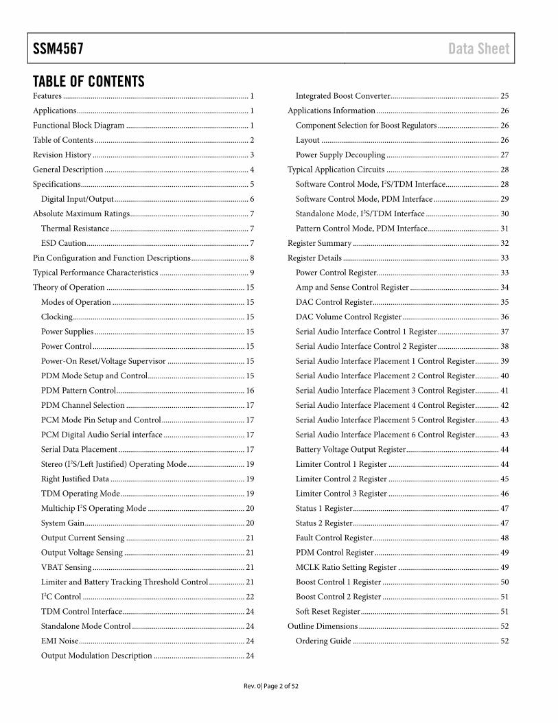
SPECIFICATIONS VBAT = 3.6 V, IOVDD = 1.8 V, TA = 25°C, RL = 8 Ω + 33 µH, VBST = 5.1 V, 20 Hz to 20 kHz bandwidth (BW), unless otherwise noted. In PDM operation, PDM clock = 3.072 MHz; for PCM operation, fS = 48 kHz.
Table 1. Parameter Symbol Conditions Min Typ Max Unit AMPLIFIER CHARACTERISTICS
Output Power/Channel POUT RL = 8 Ω, THD = 1%, f = 1 kHz, 1.43 W RL = 8 Ω, THD = 10%, f = 1 kHz 1.81 W RL = 4 Ω, THD = 1%, f = 1 kHz 2.49 W RL = 4 Ω, THD = 10%, f = 1 kHz 3.17 W System Efficiency η PO = 1 W, VBAT = 3.6 V, RL = 8 Ω 89.7 % Total Harmonic Distortion +
Noise THD + N f = 1 kHz, PO = 1 W, RL = 8 Ω 0.031 %
f = 1 kHz, PO = 0.5 W, RL = 8 Ω 0.025 % Output Voltage Noise en VBST = 5.1 V, 20 kHz BW, dither input, A-weighted 21.7 µV rms Signal-to-Noise Ratio SNR A-weighted, referred to output at 1% THD 104 dB Average Switching Frequency fSW 300 kHz Full-Scale Output Voltage 0 dBFS PCM or −6 dBFS PDM input 5.17 V peak Differential Output Offset
Voltage VOOS 1.1 mV
POWER SUPPLIES Supply Voltage Range VBAT 2.5 3.6 5.2 V IOVDD 1.62 1.8 1.98 V Power Supply Rejection Ratio DC PSRR Dither input 70 dB PSRRGSM Dither input, VRIPPLE = 100 mV on VBAT at 217 Hz 90 dB Quiescent Supply Current
VBAT IVBAT VBAT = 3.6 V 4.86 mA IOVDD IVDD IOVDD = 1.8 V, PDM clock = 3.072 MHz 1.28 mA
Shutdown Current VBAT IVBAT VBAT = 3.6 V, no input clocks 0.2 1 µA IOVDD IVDD IOVDD = 1.8 V, no input clocks 2.8 µA
SHUTDOWN CONTROL Turn-On Time tWU 3 ms Turn-Off Time tSD 10 µs Output Impedance ZOUT 86 kΩ
CLOCKING AND SAMPLE RATES Input and Output Sampling
Rate, PCM fS LRCLK rate 8 192 kHz
BCLK Frequency, PCM fBCLK 2.048 24.576 MHz Input Sampling Rate, PDM fDAC_PDM_CLK 2.048 6.144 MHz Output Sampling Rate, PDM fSNS_PDM_CLK 1.024 6.144 MHz
OUTPUT SENSING Voltage Sense Signal-to-
Noise Ratio SNRV A-weighted 77 dB
Voltage Sense Full Scale VFS Output voltage at 0 dBFS PCM/−6 dBFS PDM output from ADC
6 V peak
Voltage Sense Absolute Accuracy
1.5 %
Voltage Sense Gain Drift Temperature, TA = 10°C to 60°C 1 % Current Sense Signal-to-Noise
Ratio SNRI A-weighted 72 dB
Current Sense Input Full-Scale Voltage
IFS Voltage across sense resistor with 0 dBFS PCM/ −6 dBFS PDM output from ADC
1.78 A peak

SSM4567 Data Sheet
Rev. 0| Page 6 of 52
Parameter Symbol Conditions Min Typ Max Unit Current Sense Absolute
Accuracy 1.5 %
Current Sense Gain Drift TA = 10°C to 60°C 1.5 % VBAT Sense Full-Scale Range 2 6 V VBAT Sense Absolute
Accuracy 3 %
Current and Voltage Sense Linearity
From −80 dBr to 0 dBr 1 dB
BOOST CONVERTER Output Voltage VOUT 5.1 V Input Current Limit IMAX 2.2 A Soft Start Current Limit 0.25 A Line Regulation 0.20 %/V Load Regulation 0.15 %/A Inductor 1 2.2 µH Input Capacitor 10 µF Output Capacitor 10 22 µF PMOS Switch Resistance RONP VBAT = 3.6 V, VBST = 5.1 V 80 mΩ NMOS Switch Resistance RONN VBAT = 3.6 V, VBST = 5.1 V 55 mΩ Switching Frequency fBOOSTSW 1.536 MHz Efficiency ηBOOST 200 mA output 91 %
AUTOMATIC GAIN CONTROL AGC Gain Attack Time 20 120 µs/dB AGC Gain Release Time 0.8 1.6 3.2 sec/dB Battery Inflection Point VBAT supply when threshold reduction starts 3.2 3.5 3.9 V VBAT vs. Limiter Slope 1 3 4 V/V AGC Gain Step Size 0.1875 dB
DIGITAL INPUT/OUTPUT
Table 2. Parameter Symbol Min Typ Max Unit INPUT VOLTAGE
High VIH 0.7 × IOVDD 3.6 V Low VIL −0.3 +0.3 × IOVDD V ADDR −0.3 IOVDD + 0.3 V
INPUT LEAKAGE High IIH 1 µA Low IIL 1 µA
INPUT CAPACITANCE 5 pF OUTPUT DRIVE STRENGTH 4.5 mA

Data Sheet SSM4567
Rev. 0| Page 7 of 52
ABSOLUTE MAXIMUM RATINGS Absolute maximum ratings apply at 25°C, unless otherwise noted.
Table 3. Parameter Rating VBAT Supply Voltage −0.3 V to +6 V IOVDD Supply Voltage −0.3 V to +2 V Input Voltage −0.3 V to +6 V Storage Temperature Range −65°C to +150°C Operating Temperature Range −40°C to +85°C Junction Temperature Range −65°C to +165°C Soldering Conditions JEDEC J-STD-020
Stresses at or above those listed under Absolute Maximum Ratings may cause permanent damage to the product. This is a stress rating only; functional operation of the product at these or any other conditions above those indicated in the operational section of this specification is not implied. Operation beyond the maximum operating conditions for extended periods may affect product reliability.
THERMAL RESISTANCE θJA (junction to air) is specified for the worst-case conditions, that is, a device soldered in a circuit board for surface-mount packages. θJA is determined according to JESD51-9 on a 4-layer printed circuit board (PCB) with natural convection cooling. For more information, see the AN-617 Application Note, Wafer Level Chip Scale Package at www.analog.com.
Table 4. Thermal Resistance Package Type θJA Unit 19-Ball, 1.74 mm × 2.1 mm WLCSP 57.73 °C/W
ESD CAUTION

SSM4567 Data Sheet
Rev. 0| Page 8 of 52
PIN CONFIGURATION AND FUNCTION DESCRIPTIONS
Figure 2. Pin Configuration
Table 5. Pin Function Descriptions Pin No. Mnemonic Description A1 IOVDD I/O and Digital Power A2 AGND Analog Ground A3 PGND Power Amplifier Ground A4 BSTSW Boost Switch B1 LR_SEL/ADDR Left or Right Selection for PDM Input/I2C Address B2 SEL PDM or I2S/TDM Interface Mode Select B3 SNS_PDM_CLK/FSYNC PDM Output Clock for Sense Data in PDM Mode/Frame Synchronization Clock in I2S/TDM Mode B4 BSTSW Boost Switch C1 DAC_PDM_CLK/BCLK PDM Input Clock in PDM Mode/Bit Clock in I2S/TDM Mode C2 SNS_PDM_DAT/SNS_SDATAO Sense Data Output for PDM Mode/Sense Data Output for I2S/TDM Mode C3 VBST Boost Converter Output C4 VBST Boost Converter Output D1 DAC_PDM_DAT/DAC_SDATAI PDM Data Input for DAC in PDM Mode/Serial Data Input for DAC in I2S/TDM Mode D3 PGND Power Amplifier Ground D4 OUTN Inverting Class-D Amplifier Output E1 SCL I2C Clock Signal E2 OUTP Noninverting Class-D Amplifier Output E3 VBAT External Battery Power Supply E4 SDA I2C Data Signal
BALL A1INDICATOR
AGND
LR_SEL/ADDR
VBST
PGND
PGND
SNS_PDM_CLK/FSYNC
BSTSW
SEL
VBSTSNS_PDM_DAT/SNS_SDATAO
IOVDD
VBAT SDA
DAC_PDM_DAT/DAC_SDATAI
DAC_PDM_CLK/BCLK
SCL OUTP
OUTN
BSTSW
1 2 3 4
A
B
C
D
E
1227
8-00
2

Data Sheet SSM4567
Rev. 0| Page 9 of 52
TYPICAL PERFORMANCE CHARACTERISTICS
Figure 3. THD + N vs. Output Power at RL = 8 Ω and 33 µH
Figure 4. THD + N vs. Output Power at RL = 4 Ω and 15 µH
Figure 5. THD + N vs. Frequency at VBAT = 5 V, RL = 8 Ω and 33 µH
Figure 6. THD + N vs. Frequency at VBAT = 4.2 V, RL = 8 Ω and 33 µH
Figure 7. THD + N vs. Frequency at VBAT = 3.6 V, RL = 8 Ω and 33 µH
Figure 8. THD + N vs. Frequency at VBAT = 2.5 V, RL = 8 Ω and 33 µH
0.001
0.01
0.1
1
10
100
0.00001 0.0001 0.001 0.01 0.1 1 10
THD
+ N
(%)
OUTPUT POWER (W)
VDD = 2.5VVDD = 3.0VVDD = 3.6VVDD = 4.2VVDD = 5.0V
1227
8-10
3
0.001
0.01
0.1
1
10
100
0.00001 0.0001 0.001 0.01 0.1 1 10
THD
+ N
(%)
OUTPUT POWER (W)
VDD = 2.5VVDD = 3.0VVDD = 3.6VVDD = 4.2VVDD = 5.0V
1227
8-10
4
0.001
0.01
0.1
1
10
10 100 1k 10k 100k
THD
+ N
(%)
FREQUENCY (Hz)
POUT = 50mWPOUT = 250mWPOUT = 500mWPOUT = 1W
1227
8-10
5
0.001
0.01
0.1
1
10
10 100 1k 10k 100k
THD
+ N
(%)
FREQUENCY (Hz)
POUT = 50mWPOUT = 250mWPOUT = 500mWPOUT = 1W
1227
8-10
6
0.001
0.01
0.1
1
10
10 100 1k 10k 100k
THD
+ N
(%)
FREQUENCY (Hz)
POUT = 50mWPOUT = 250mWPOUT = 500mWPOUT = 1W
1227
8-10
7
0.001
0.01
0.1
1
10
10 100 1k 10k 100k
THD
+ N
(%)
FREQUENCY (Hz)
POUT = 50mWPOUT = 250mWPOUT = 500mWPOUT = 1W
1227
8-10
8

SSM4567 Data Sheet
Rev. 0| Page 10 of 52
Figure 9. THD + N vs. Frequency at VBAT = 5 V, RL = 4 Ω and 15 µH
Figure 10. THD + N vs. Frequency at VBAT = 4.2 V, RL = 4 Ω and 15 µH
Figure 11. THD + N vs. Frequency at VBAT = 3.6 V, RL = 4 Ω and 15 µH
Figure 12. THD + N vs. Frequency at VBAT = 2.5 V, RL = 4 Ω and 15 µH
Figure 13. Quiescent Current vs. VBAT Supply Voltage
Figure 14. Output Power vs. Frequency at RL = 8 Ω, THD + N = 1%
0.001
0.01
0.1
1
10
10 100 1k 10k 100k
THD
+ N
(%)
FREQUENCY (Hz)
POUT = 250mWPOUT = 500mWPOUT = 1WPOUT = 1.4W
1227
8-10
9
0.001
0.01
0.1
1
10
10 100 1k 10k 100k
THD
+ N
(%)
FREQUENCY (Hz)
POUT = 250mWPOUT = 500mWPOUT = 1WPOUT = 1.4W
1227
8-11
0
0.001
0.01
0.1
1
10
10 100 1k 10k 100k
THD
+ N
(%)
FREQUENCY (Hz)
POUT = 250mWPOUT = 500mWPOUT = 1WPOUT = 1.4W
1227
8-11
1
0.001
0.01
0.1
1
10
10 100 1k 10k 100k
THD
+ N
(%)
FREQUENCY (Hz)
POUT = 250mWPOUT = 500mWPOUT = 1WPOUT = 1.4W
1227
8-11
2
0
1
2
3
4
5
6
7
8
2.5 3.0 3.5 4.0 4.5 5.0 5.5
QU
IESC
ENT
CU
RR
ENT
(mA
)
VBAT (V)
8Ω + 33mHNO LOAD
1227
8-11
3
0
0.5
1.0
1.5
2.0
2.5
200 2000 20000
OU
TPU
T PO
WER
(W)
FREQUENCY (Hz)
2.5V3.0V3.6V4.2V5.0V
1227
8-11
4

Data Sheet SSM4567
Rev. 0| Page 11 of 52
Figure 15. Output Power vs. Frequency at RL = 4 Ω, THD + N = 1%
Figure 16. Efficiency vs. Output Power, Boost Inductor = 2.2 µH,
RL = 8 Ω and 33 µH
Figure 17. Efficiency vs. Output Power, Boost Inductor = 2.2 µH,
RL = 4 Ω and 15 µH
Figure 18. Boost Efficiency vs. Output Current, Boost Inductor = 2.2 µH
at 3.072 MHz
Figure 19. Output Voltage vs. VBAT Supply Voltage, Limiter Threshold = 5.4 V
Figure 20. Output Voltage vs. Input Amplitude
0
0.5
1.0
1.5
2.0
2.5
3.0
3.5
4.0
4.5
200 2k 20k
POW
ER O
UTP
UT
(W)
FREQUENCY (Hz)
2.5V3.0V3.6V4.2V5.0V
1227
8-11
5
0
10
20
30
40
50
60
70
80
90
100
0 0.5 1.0 1.5 2.0
EFFI
CIE
NCY
(%)
OUTPUT POWER ( W)
VBAT = 2.5VVBAT = 3.0VVBAT = 3.6VVBAT = 4.2VVBAT = 5.0V
1227
8-11
6
0
10
20
30
40
50
60
70
80
90
100
EFFI
CIE
NCY
(%)
OUTPUT POWER (W)
0 0.5 1.0 1.5 2.0 2.5 3.0 3.5
VBAT = 2.5VVBAT = 3.0VVBAT = 3.6VVBAT = 4.2VVBAT = 5.0V
1227
8-11
7
0
10
20
30
40
50
60
70
80
90
100
EFFI
CIE
NCY
(%)
LOAD CURRENT (mA)
0 200 400 600 800 1000 1200
VBAT = 2.5VVBAT = 3.0VVBAT = 3.6VVBAT = 4.2VVBAT = 5.0V
1227
8-11
8
0
0.5
1.0
1.5
2.0
2.5
3.0
3.5
4.0
2.5 3.0 3.5 4.0 4.5 5.0
OU
TPU
T VO
LTA
GE
(V rm
s)
VBAT (V)
SLOPE = 2V/V, VBAT_INF = 3.7VSLOPE = 2V/V, VBAT_INF = 3.5VSLOPE = 2V/V, VBAT_INF = 3.3VSLOPE = 3V/V, VBAT_INF = 3.7VSLOPE = 3V/V, VBAT_INF = 3.5VSLOPE = 3V/V, VBAT_INF = 3.3V
1227
8-11
9
0.5
1
2
4
–20 –15 –10 –5
OU
TPU
T VO
LTA
GE
(V rm
s)
INPUT AMPLITUDE (dBFS)
2.5V2.7V2.9V3.1V3.3V3.5V3.7V3.9V4.1V
1227
8-12
0

SSM4567 Data Sheet
Rev. 0| Page 12 of 52
Figure 21. Power Supply Rejection Ratio (PSRR) vs. Frequency, RL = 8 Ω
Figure 22. Output Spectrum vs. Frequency (FFT), Output Power = 100 mW,
RL = 8 Ω, 1 kHz input
Figure 23. Linearity of the Voltage Sense vs. Input Level, RL = 8 Ω and 33 µH
Figure 24. Linearity of the Current Sense vs. Input Level, RL = 8 Ω and 33 µH
Figure 25. VBAT ADC Sense Level Output vs. VBAT Supply Voltage, RL = 8 Ω
Figure 26. Current Sense THD + N vs. Output Power, RL = 8 Ω and 33 µH
FREQUENCY (Hz)
–100
–90
–80
–70
–60
–50
–40
–30
–20
–10
0
100 1k 10k
PSR
R (d
B)
2.5V3.0V3.6V4.2V5.0V
1227
8-12
1
FREQUENCY (Hz)
–140
–120
–100
–80
–60
–40
–20
0
20 200 2000 20000
OU
PUT
SPEC
TRU
M (d
BV)
2.5V3.6V5.0V
1227
8-12
2
–0.10
–0.08
–0.06
–0.04
–0.02
0
0.02
0.04
0.06
0.08
–60 –50 –40 –30 –20 –10 0
LIN
EAR
ITY
(dB
)
INPUT (dBFS )
VBAT = 2.5VVBAT = 3.0VVBAT = 3.6VVBAT = 4.2VVBAT = 5.0V
1227
8-12
3
–0.2
–0.1
0
0.1
0.2
0.3
0.4
0.5
0.6
0.7
–60 –50 –40 –30 –20 –10 0
LIN
EAR
ITY
(dB
)
INPUT (dBFS)
VBAT = 2.5VVBAT = 3.0VVBAT = 3.6VVBAT = 4.2VVBAT = 5.0V
1227
8-12
4
2.5
3.0
3.5
4.0
4.5
5.0
2.5 3.0 3.5 4.0 4.5 5.0
VBAT
SEN
SE O
UTP
UT
(V)
VBAT (V) 1227
8-12
5
0.01
0.1
1
10
100
0.00001 0.0001 0.001 0.01 0.1 1 10
THD
+ N
(%)
OUTPUT POWER (W)
VBAT = 2.5VVBAT = 3.0VVBAT = 3.6VVBAT = 4.2VVBAT = 5.0V
1227
8-12
6

Data Sheet SSM4567
Rev. 0| Page 13 of 52
Figure 27. Voltage Sense THD + N vs. Output Power, RL = 8 Ω and 33 µH
Figure 28. Current Sense THD + N vs. Output Power, RL = 4 Ω and 15 µH
Figure 29. Voltage Sense THD + N vs. Output Power, RL = 4 Ω and 15 µH
Figure 30. Voltage Sense THD + N vs. Frequency, VBAT = 3.6 V,
RL = 8 Ω and 33 µH
Figure 31. Current Sense THD + N vs. Frequency, VBAT = 3.6 V,
RL = 8 Ω and 33 µH
Figure 32. Voltage Sense THD + N vs. Frequency, VBAT = 3.6 V,
RL = 4 Ω and 15 µH
OUTPUT POWER (W)
0.01
0.1
1
10
100
0.00001 0.0001 0.001 0.01 0.1 1 10
THD
+ N
(%)
VBAT = 2.5VVBAT = 3.0VVBAT = 3.6VVBAT = 4.2VVBAT = 5.0V
1227
8-12
7
OUTPUT POWER (W)
0.01
0.1
1
10
100
0.00001 0.0001 0.001 0.01 0.1 1 10
THD
+ N
(%)
1227
8-12
8
VBAT = 2.5VVBAT = 3.0VVBAT = 3.6VVBAT = 4.2VVBAT = 5.0V
OUTPUT POWER (W)
0.01
0.1
1
10
100
0.00001 0.0001 0.001 0.01 0.1 1 10
THD
+ N
(%)
1227
8-12
9
VBAT = 2.5VVBAT = 3.0VVBAT = 3.6VVBAT = 4.2VVBAT = 5.0V
0.001
0.01
0.1
1
10
10 100 1k 10k 100k
THD
+ N
(%)
FREQUENCY (Hz)
POUT = 50mWPOUT = 250mWPOUT = 500mWPOUT = 1W
1227
8-13
0
0.001
0.01
0.1
1
10
10 100 1k 10k 100k
THD
+ N
(%)
FREQUENCY (Hz)
POUT = 50mWPOUT = 250mWPOUT = 500mWPOUT = 1W
1227
8-13
1
0.001
0.01
0.1
1
10
10 100 1k 10k 100k
THD
+ N
(%)
FREQUENCY (Hz) 1227
8-13
2
POUT = 250mWPOUT = 500mWPOUT = 1WPOUT = 1.4W

SSM4567 Data Sheet
Rev. 0| Page 14 of 52
Figure 33. Current Sense THD + N vs. Frequency, VBAT = 3. 6 V,
RL = 4 Ω and 15 µH
Figure 34. Output Spectrum of Sense ADC vs. Frequency
Output Power = 100 mW, RL = 8 Ω
0.001
0.01
0.1
1
10
10 100 1k 10k 100k
THD
+ N
(%)
FREQUENCY (Hz)
POUT = 250mWPOUT = 500mWPOUT = 1WPOUT = 1.4W
1227
8-13
3 –140
–120
–100
–80
–60
–40
–20
0
20 200 2k 20k
OU
TPU
T SP
ECTR
UM
(dB
V)
FREQUENCY (Hz) 1227
8-13
4
ISENSEVSENSE

Data Sheet SSM4567
Rev. 0| Page 15 of 52
THEORY OF OPERATION MODES OF OPERATION The SSM4567 has several modes of control and audio I/O operation. Audio and sense data can be sent to and from the SSM4567 in 1-bit PDM format by tying the SEL pin to AGND or multibit PCM format by tying the SEL pin to IOVDD. With PCM data, the serial audio interface can be configured for I2S, left justified, or TDM formatting. The SSM4567 can be controlled using I2C, PDM pattern control, TDM control, or standalone operation. See Table 10 for more details.
CLOCKING The SSM4567 requires a clock present at the DAC_PDM_CLK/ BCLK input pin to operate. This clock must be fully synchronous with the incoming digital data. The clock frequencies must fall in the range of 2.048 MHz to 24.576 MHz for PCM mode, or 2.048 MHz to 6.144 MHz for PDM mode.
In standalone I2S mode, the required clock must be present on the SNS_PDM_CLK/FSYNC pin.
POWER SUPPLIES The SSM4567 requires two power supplies: VBAT and IOVDD.
VBAT
VBAT supplies power to the boost converter and its associated drive, control, and protection circuitry. VBAT can operate from 2.5 V to 5.2 V and must be present to obtain audio output.
IOVDD
IOVDD provides power to the digital logic circuitry and the I/O drive circuitry. IOVDD can operate from 1.62 V to 1.98 V and must be present to obtain audio output.
Power Sequencing
On device power-up, VBAT must be applied to the device first. The timing of the IOVDD following VBAT is not important. See the Power-On Reset/Voltage Supervisor section for more details.
POWER CONTROL The SSM4567 can be powered down by several methods. If using I2C or TDM control, a software power-down control SPWDN fully powers down the device. PDM pattern control has a standby pattern that powers down all blocks except the PDM interface.
For lowest power shutdown, the SSM4567 also contains a clock loss detection circuit that looks at the DAC_PDM_CLK/BCLK input clock. When DAC_PDM_CLK/BCLK is absent, the device automatically powers down all internal circuitry to its lowest power state. When DAC_PDM_CLK/BCLK returns, the device automatically powers up following its usual power sequence.
There is an optional automatic power-down feature in which the device enters a lower power state after 2048 consecutive zero input samples have been received when in PCM operation. Only the I2C and digital audio input blocks remain active.
The output current, output voltage, and VBAT sensing can be turned off independently via the ISNS_PWDN, VSNS_PWDN, and BSNS_PWDN control bits. This can save power if the amplifier operation is needed but not the output sensing.
The amplifier and boost converter can be powered down independently via the AMP_PWDN and BOOST_PWDN control bits. When the boost is powered down and the amplifier is still active, the amplifier runs directly from the VBAT supply. This same VBAT only operation can be entered with the boost still active with the VBAT_ONLY bit. The amplifier can be powered down with the boost still enabled so the boost output can be used for other functions.
POWER-ON RESET/VOLTAGE SUPERVISOR The SSM4567 includes an internal power-on reset and voltage supervisor circuit. This circuit provides an internal reset to all circuitry whenever VBAT or IOVDD is substantially below the nominal operating threshold. This simplifies supply sequencing during initial power-on.
The circuit also monitors the power supplies to the IC. If the supply voltages fall below the nominal operating threshold, this circuit stops the output and issues a reset. This ensures that no damage occurs due to low voltage operation and that no pops can occur under nearly any power removal condition.
PDM MODE SETUP AND CONTROL The SSM4567 can operate using 1-bit PDM data for both its input and for the sense outputs. In PDM mode, control can be done either by PDM control patterns or with I2C. If the SEL pin is tied to AGND, the SSM4567 starts up and operate in PDM pattern control mode.
The SSM4567 can also operate in PDM via I2C control mode. A regular I2C operating address can be set on the LR_SEL/ADDR pin. Then, using I2C, the device can be set into PDM mode by writing a 1 to the PDM_MODE control bit. The PDM_LR_SEL bit selects which input channel is used.
In PDM operating mode mode, the 1-bit PDM input to the DAC is received on the DAC_PDM_DAT/DAC_SDATAI pin. The DAC_PDM_CLK/BCLK pin provides the system clock and is used for clocking in the input data. Output voltage and current sense are output on the SNS_PDM_DAT/SNS_SDATAO pin. The output can be sent at a different rate from the input, and the SNS_PDM_CLK/FSYNC pin determines the sense output rate. Alternatively, the output rate can be sent at the same rate as the input and only one clock pin, DAC_PDM_CLK/BCLK, is needed to operate the device. To use only one clock, set the SHARED_CLOCK register to 1.
Full-scale voltage for both the input and output is mapped to −6 dBFS on the PDM stream.
The PDM data input is registered directly on each clock edge. The data transition on the PDM data output is delayed relative to the clock edge.

SSM4567 Data Sheet
Rev. 0| Page 16 of 52
Table 6. PDM Timing Parameters
Parameter Limit
Unit Description tMIN tMAX tFALL 10 ns Clock fall time tRISE 10 ns Clock rise time tSETUP 10 ns Data setup time tHOLD 7 ns Data hold time
Figure 35. PDM Input Data Format
The PDM data is output on both edges of the clock. The current sense ADC data is output when SNS_PDM_CLK/FSYNC is high and should be read on the falling edge. The voltage sense ADC data is output when SNS_PDM_CLK/FSYNC is low and should be read on the rising edge.
Figure 36. SDATA (DAC_SDATAI/SNS_SDATAO) Output in PDM Mode
By default in PDM mode, PDM pattern control is used for control information. I2C control can be used instead, but do not use both at the same time. If PDM pattern control is engaged, then registers associated with the PDM pattern control do not function using I2C. Writes to those registers are ignored and reads do not reflect the current state of the device. For I2C control, it is best to tie the SEL pin to IOVDD and then set the PAT_CTRL_EN bit to 0 to disable PDM pattern control before any other I2C writes or reads are performed. By default, the I2C device address in PDM mode is 0x34. By setting the I2C_ADDR_SET bit, the device address can be either 0x34 or 0x35, depending on the state of the LR_SEL/ADDR pin.
PDM PATTERN CONTROL PDM mode operation has a simple control mechanism that can set the device for low power states and control functionality. This is accomplished by sending a repeating 8-bit pattern to the device. Different patterns set different functionalities.
Any pattern must be repeated a minimum of 128 times. The device is automatically muted when a pattern is detected so that a pattern can be set while the device is operational without a pop/click due to pattern transition. After this minimum repetition is complete, the pattern can be removed at any time and the device resumes normal operation.
All patterns except mute and power-down are sticky, in that after the pattern is sent the functionality of the pattern remains after the pattern is removed. Mute and power-down are active only when their respective patterns are being continuously written.
All functionality set via patterns return to its default values after a clock loss power-down or after the device reset pattern is sent.
Table 7. PDM Watermarking Pattern Control Descriptions Pattern Control Description Register Setting 0xD2 Limiter: enable. LIM_EN = 01 0xD4 Lower gain mode (3.6 V) with
−6 dBFS). ANA_GAIN = 0
0xD8 Shared clock operation. Only DAC_PDM_CLK is needed.
SHARED_CLOCK = 1
0xE1 Ultralow EMI mode. Edges = 1 0xE2 Low latency mode with
pattern delay (~15 µs latency). LOW_LATENCY = 01
0xE4 Set DAC to low power mode = off. PDM_CLK = 128 × fS mode.
DAC_LPM = 0
0xAA Device reset: place the device into default configuration
0x66 Mute. DAC_MUTE = 1 0xAC Power-down: all blocks off
except for PDM interface. Normal start-up time.
SPWDN = 1
0xF1 Limiter: 3.7 V battery inflection point.
VBAT_INF = 010
0xF2 Limiter: 3.3 V battery inflection point.
VBAT_INF = 110
0xF4 Limiter: 2 V/V VBAT vs. the limiter slope.
Slope = 01
0xC1 Sense power-up/power-down toggle.
Toggle value of BSNS_PWDN, ISNS_PWDN, and VSNS_PTWN
0xC2 Limiter: threshold value set to 5.4 V peak.
LIM_THRES = 0110
tHOLD
LDATA
DAC_SDATAI
BCLK
LDATA
RDATA
RDATA
tSETUP
1227
8-00
8
BCLK
FSYNC
SDATA I V I V I V I V I V I IV 1227
8-00
9

Data Sheet SSM4567
Rev. 0| Page 17 of 52
PDM CHANNEL SELECTION The SSM4567 includes a left/right input select pin, LR_SEL/ADDR (see Table 24) that determines which of the time-multiplexed input streams is routed to the amplifier when using PDM pattern control mode. To select the left input channel, connect LR_SEL/ADDR pin to AGND. To select right channel data, connect LR_SEL/ADDR pin to IOVDD. At any point during amplifier operation, the logic level applied to LR_SEL/ADDR pin can be changed and the output switches between input streams without audible artifacts. Aside from logic level selection from the user, no muting, watermarking pattern, or synchronizing is necessary to achieve a click/pop free LR_SEL/ADDR transition.
Table 8. LR_SEL/ADDR Function Descriptions Device Setting LR_SEL/ADDR Pin Configuration Right Channel Select IOVDD
Left Channel Select GND
PCM MODE PIN SETUP AND CONTROL When the SEL pin is tied to IOVDD, the SSM4567 is set for PCM mode operation. In this mode, the SSM4567 supports standalone operation, I2C control, or can be controlled using commands sent over the input serial audio/TDM interface. When the LR_SEL/ADDR pin is pulled up via a 47 kΩ resistor, the IC operates in standalone mode with most registers set to their default states.
The state of the several pins can change the functionality of other pins. The LR_SEL/ADDR pin determines the I2C device address. In standalone and TDM control modes, the SCL and SDA pins are used to determine the TDM slot used. See Table 10 for details.
PCM DIGITAL AUDIO SERIAL INTERFACE The SSM4567 includes a standard serial audio interface that is slave only. The interface is capable of receiving and transmitting I2S, left justified, PCM, or TDM formatted data.
There is an input interface for sending audio to the amplifier and an output interface for the sense data. These interfaces share the same FSYNC and BCLK signals.
A BCLK signal must be provided to the SSM4567 for correct operation. The BCLK signal must have a minimum frequency of 2 MHz. The BCLK signal is used for internal clocking of the device. The BCLK rate is automatically detected, but the sampling frequency must be known to the device. The BCLK rates at 32 kHz to 48 kHz that are supported are 50, 64, 100, 128, 192, 200, 256, 384, 400, and 512 times the sample rate.
The serial interfaces have three main operating modes. Stereo mode, typically I2S or left justified, is used when there is a single chip on the interface bus. TDM mode is more flexible and offers the ability to have multiple chips on the bus. The third operating mode is multichip I2S mode, which uses standard I2S formatting but allows multiple chips to use the bus.
It is also possible to use the serial interfaces for bidirectional control information. When this is done, the internal control reg-isters are accessed via the serial audio interface and not from I2C.
These mode selections can be set via the I2C interface with the SAI_MODE and MC_I2S bits. Alternatively, in standalone mode or when AUTO_SAI is set to 1, the interface can auto-configure based on how the signals are connected to the clock pins and the FSYNC type (pulse or 50% duty cycle).
When in standalone or automatic configuration modes, an I2S interface format can be selected by swapping the pin connections for the BCLK and FSYNC signals (with the I2S LRCLK signal connected to the DAC/PDM_CLK/BCLK pin and BCLK signal connected to the SNS_PDM_CLK/FSYNC pin). When the BCLK and FSYNC signals are connected to their respective pins, and the FYSNC signal is a single BCLK cycle pulse, TDM mode is selected. When the BCLK and FSYNC signals are connected to their respective pins, and the FYSNC signal is a 50% duty cycle signal, multichip I2S mode is selected.
On the SNS_PDM_DAT/SNS_SDATAO pin, unused cycles can either be driven or set to high-Z. This is determined by the SAI_DRV control bit. If multiple chips are used on the serial interface bus, then SAI_DRV must be set to 0 so that unused cycles are not driven.
SERIAL DATA PLACEMENT The SSM4567 is flexible in where within a frame it places output data and where it looks for input data. There are four control bits for when input data is expected (Px_DAC) and and six control bits for when output data is driven (Px_SNS).
A single data frame is broken up into individual fields, referred to as placements. Each placement can be 8 bits, 16 bits, or 24 bits in length. A single frame on the TDM or I2S data stream can contain several data placements of varying length.
When the serial port is operating in TDM mode, placements start directly after the FSYNC pulse. The first placement is referred to as P1, the second placement is referred to as P2, and so on, increasing sequentially. These placements appear in sequential order on the serial data signal. Up to four placements can be on the input stream and up to six placements can be on the output stream. Figure 37 shows a basic timing diagram of the placements in TDM mode.
When the serial port is operating in I2S mode, placements start directly after the FSYNC falling clock edge, signalling the beginning of a new frame. The first placement is referred to as P1, the second placement is referred to as P2, and so on, increasing sequentially. The odd-numbered placements (P1, P3, and P5) appear sequentially in the left channel, when the FSYNC signal is low (assuming FSYNC_MODE = 0), and the even-numbered placements (P2, P4, and P6) appear sequentially in the right channel, when the FSYNC signal is high (assuming that FSYNC_MODE = 0. Up to four placements can be on the input stream and up to six placements can be on the output stream.
SSM4567 Data Sheet
Rev. 0| Page 18 of 52
Figure 38 shows a basic timing diagram of the placements in I2S mode.
The corresponding registers allow configuration of each data placement. An input placement (Px_DAC) can carry 24-bit audio data, 16-bit audio data, or eight zero bits that are used as padding and ignored. See the Right Justified Data section for more information about using the 8 zero bits settings. A sense placement (Px_SNS) can contain 16-bit voltage output data, 16-bit
current output data, 8-bit battery voltage data, 8-bit control data, alternating 16-bit voltage and current data, 8-bit status data, 8-bit V/I marker and slot ID data, or 8 zero bits.
For standard I2S mode, the serial input is configured to receive mono audio data, and the serial output is configured to send voltage, current, and battery data back to the host device. The corresponding registers are in Table 9 and the corresponding timing diagram is in Figure 39.
Table 9. Standard I2S Data Placement Settings Register Bit Field Setting Description BCLK_POL 0b0 Rising edge of BCLK is used to latch data FSYNC_MODE 0b0 FSYNC low corresponds to left data channel SDATA_FMT 0b0 Data MSB is delayed by one bit clock cycle SAI_MODE 0b0 Stereo mode MC_I2S 0b0 Normal I2S operation P1_DAC 0b00 24-bit audio input data is in input Placement P1 P1_SNS 0b000 16-bit sense voltage is in output Placement P1 P2_SNS 0b001 16-bit sense current is in output Placement P2 P3_SNS 0b010 8-bit battery voltage is in Placement P3
Table 10. PCM Modes Pin Setup List
Control Mode
I2C Control Address1
TDM Slot
Signals Connected To Pins For Modes Listed In The First Three Columns
LR_SEL/ADDR SCL SDA SEL DAC_PDM_CLK/ BCLK
SNS_PDM_CLK/ FSYNC
I2C 0 (0x34) 1 AGND SCL SDA IOVDD Bit clock Frame sync 1 (0x35) 2 IOVDD SCL SDA IOVDD Bit clock Frame sync 2 (0x36) 3 Open SCL SDA IOVDD Bit clock Frame sync
Standalone (TDM Interface)
N/A 1 47 kΩ pull-up AGND AGND IOVDD Bit clock Frame sync N/A 2 47 kΩ pull-up AGND IOVDD IOVDD Bit clock Frame sync N/A 3 47 kΩ pull-up IOVDD AGND IOVDD Bit clock Frame sync N/A 4 47 kΩ pull-up IOVDD IOVDD IOVDD Bit clock Frame sync
Standalone (I2S Interface)
N/A N/A 47 kΩ pull-up Boost power down (active low)
Shutdown (active low)
IOVDD Frame sync (intentional swap of CLK pins, Pin B3 and Pin C1)
Bit clock (intentional swap of CLK pins, Pin B3 and Pin C1)
TDM N/A 1 47 kΩ pull-down AGND AGND IOVDD Bit clock Frame sync N/A 2 47 kΩ pull-down AGND IOVDD IOVDD Bit clock Frame sync N/A 3 47 kΩ pull-down IOVDD AGND IOVDD Bit clock Frame sync N/A 4 47 kΩ pull-down IOVDD IOVDD IOVDD Bit clock Frame sync
1 N/A means not applicable.
Figure 37. Basic Timing Diagram of Placements in TDM Stream
P1
8 BITS/16 BITS/24 BITS
BCLK
FSYNC
DAC_SDATAI P2 Px
1227
8-01
0

Data Sheet SSM4567
Rev. 0| Page 19 of 52
Figure 38. Basic Timing Diagram of Placements in I2S Stream
Figure 39. Standard I2S Data Placement Timing Diagram
Figure 40. TDM Serial Interface Format
STEREO (I2S/LEFT JUSTIFIED) OPERATING MODE Stereo modes use both edges of the FSYNC signal to determine placement of data. Stereo mode is enabled when SAI_MODE = 0 and I2S or left justified is determined by the SDATA_FMT bit setting. In standalone mode or when AUTO_SAI = 1, an I2S output interface can be configured by exchanging the connections to the DAC_PDM_CLK/BCLK and SNS_PDM_CLK/FSYNC pins.
The I2S and left justified interface formats accept any number of BCLK cycles per FSYNC cycle. Sample rates from 8 kHz to 192 kHz are accepted.
The six placement control registers, SAI_PLACEMENT_x, determine placement of input and output data. Odd numbered placement control registers determine the order on the left channel and even number on the right channel. In the timing diagrams, these placements are refered to as P1 to P6. There are four placements for the incoming DAC data and six placements for the outgoing sense data.
RIGHT JUSTIFIED DATA When the audio data in either a TDM or I2S slot placement is right justified, the Px_DAC bits can be used to properly read the data. Each Px_DAC bit has a setting where it reads in eight bits of data. The data is then not used and fulfills the read requirement for that slot so that the subsequent bits are read as the data of the next slot. This continues until a slot is reached that is set to read audio data.
For example, for a stereo I2S, 24-bit audio data-word that is right justified with 32 BCLKS for the left channel, set P1_DAC to b10 so that it picks up the first eight bits of zero data. Then, set P2_DAC to b00 so that it picks up the 24-bit audio data.
Fo another example, for a stereo I2S 16-bit audio data word that is right justified with 32 BCLKS for the left channel, set P1_DAC to b10 so that it picks up the first eight bits of zero data.Then, set P2_DAC to b10 so that it picks up the next blank 8 bits of data, and set P3_DAC to b01 so it then picks up the 16 bits of audio data.
TDM OPERATING MODE TDM operating mode allows multiple chips to use a single serial interface bus.
The FSYNC signal on the SNS_PDM_CLK/FSYNC pin operates at the desired sample rate. The rising edge of the FSYNC signal indicates the start of a new frame. For proper operation, this signal must be one BCLK cycle wide, transitioning on a falling BCLK signal edge. The MSB of data is present on the SNS_PDM_DAT/SNS_SDATAO pin one BCLK cycle later. The SNS_PDM_DAT/ SNS_SDATAO signal must be latched on a rising edge of the BCLK signal (see Figure 40).
P1
8 BITS/16 BITS/24 BITS
BCLK
FSYNC
DAC_SDATAI P3 P2 P4
1227
8-01
1
VOLTAGE
16 BCLKs 16 BCLKs
BATTERY CURRENT
DAC INPUT
8 BCLKs
BCLK
FSYNC
DAC_SDATAI
DAC_SDATAO
1227
8-01
2
DAC DATA 1
ISENSE 1 VSENSE 1
BCLK
FSYNC
DAC_SDATAI
DAC_SDATAO
24
16 16
32 BCLKS
1227
8-01
3
DAC DATA 2
ISENSE 2

SSM4567 Data Sheet
Rev. 0| Page 20 of 52
Each chip on the TDM bus can occupy 32, 48, or 64 BCLK cycles. This is set with the TDM_BCLKS control register and all chips on the bus must have the same setting. Up to eight SSM4567 chips can be used on a single TDM bus, but only three unique I2C device addresses are available. The SSM4567 automatically determines how many possible chips can be placed on the bus from the BCLK rate. There is no limit to the total number of BCLK cycles per FSYNC pulse. In standalone mode, only four slots can be used because there are only four combinations of the SDA and SCL pins to choose from (see Table 10).
When not in standlone mode, the slot that each SSM4567 uses is determined either by the LR_SEL/ADDR pin settings or the TDM_SLOT control register. By default, the setting is determined by the state of the LR_SEL/ADDR pin, which allows the first three slots to be selected. However, it can be overridden by the TDM_SLOT control register, which allows eight different slots to be selected.
Table 11. TDM Slot Selection Device Setting LR_SEL/ADDR Pin Configuration TDM Chip 1 Slot Used/Driven Tied to AGND TDM Chip 2 Slot Used/Driven Tied to IOVDD TDM Chip 3 Slot Used/Driven Open
The six placement control bits determine placement of input and output data within each chip slot. Input data to the DAC, using the DAC_PDM_DAT/DAC_SDATAI pin, can be either 16-bit or 24-bit data or it can be set to read in eight bits and ignore them. This is useful for right justified data formats where the first eight bits of the 32 bit clocks are padded zeros. The first placement register is set to read in eight bits and ignore them. Then the next placement register is set to read in the 24-bit audio data.
The output data from the DAC, using the SNS_PDM_DAT/ SNS_SDATAO pin, can be any of the following:
• 16-bit voltage output • 16-bit current output • 8-bit battery (VBAT) voltage • 8-bit control data output • Alternating 16-bit voltage and current • 8-bit status output • 8-bit V/I marker and slot ID • Blank eight bits
It is possible to have as many as six output placements and four input placements per frame depending on the clock rates.
MULTICHIP I2S OPERATING MODE A special multichip I2S mode is enabled by setting the MC_I2S control register (Register 0x05[4]) to 1 when under I2C control. The TDM_SLOT register (Register 0x05[2:0]) sets the slot where data is expected and sense data is transmitted. In standalone mode or when AUTO_SAI = 1, multichip I2S is enabled when the device is wired for TDM mode (that is, the BCLK and
FSYNC signals are not swapped as they would be for I2S/left justified operation) except the FSYNC signal has a 50% duty cycle. The frequency of the FSYNC signal in relation to the BCLK signal determines if the device is in two-chip or four-chip mode. If the FSYNC signal consists of one BCLK cycle pulse, TDM operating mode is active instead.
The multichip I2S interface allows multiple chips to drive a single I2S bus. Each chip takes control of the bus every two or four frames (depending on the number of chips placed on the bus), allowing a maximum of four chips on the bus. Each frame or cycle of the FSYNC signal must 64 BCLK cycles long. The LR_SEL/ADDR pin assignments determine the order of control. Each frame also contains a slot ID code that is appended to the current data in the frame. This code indicates the slot of the chip that sent the data for that frame.
The mapping of LR_SEL/ADDR pin assignments to the ID tag when not in standalone mode is shown in Table 12.
Table 12. Multichip I2S Slot Configuration in SA Mode ADDR Pin Configuration Slot No. ID Tag Tied to AGND 1 0001 Tied to IOVDD 2 0010 Open 3 0100
The device automatically configures for two-chip or four-chip depending on the number of detected chips in the bus. For two-chip operation, the first and second slots must be used. Unused slots are allowed; however, Slot 1 must always be used. To enable two-chip operation, the device starts in four-chip operation and, when it is detected that Slot 3 and Slot 4 are unused, it switches to two-chip operation.
Table 13 describes the FSYNC and BCLK rates that are supported in multichip I2S mode.
Table 13. FSYNC and BCLK Rates For Multichip I2S Sample Rate Valid Slots FSYNC Rate BCLK Rate 32 kHz to 48 kHz 1, 2 2 × fS
(32 kHz to 96 kHz)
128 × fS (2.048 MHz to 6.144 MHz)
32 kHz to 48 kHz 1, 2, 3, 4 4 × fS (64 kHz to 128 kHz)
256 × fS (4.096 MHz to 12.288 MHz)
SYSTEM GAIN The default analog gain of the SSM4567 maps a 0 dBFS input level to 5.1 V peak nominally at the amplifier output. This setting provides optimal gain staging for best noise performance.
A lower analog gain setting that maps a 0 dBFS input level to 3.6 V peak can be set via the ANA_GAIN bit, Register 0x01[0].
There is also digital gain/volume control, Register 0x03, that provides fine control in 0.375 dB steps from −71.25 dB to +24 dB. There is one additional step for mute.

Data Sheet SSM4567
Rev. 0| Page 21 of 52
OUTPUT CURRENT SENSING The SSM4567 uses an on-chip sense resistor to determine the output current flowing to the load. The voltage across this sense resistor is proportional to the load current and sent to an ADC running nominally at 128 × fs. In PCM mode, the output of this ADC is downsampled using digital filtering. This downsampled signal at an 8 kHz to 192 kHz sample rate is output on the digital audio interface. The data is 16 bits and in signed fraction format. For both current and voltage sensing a sample rate equal to the DAC input is the default setting. A lower sample rate of ½, ¼, or ⅛ the DAC sample rate can be used. This can be set using the SNS_FS bits, Register 0x01[5:4].
In PDM mode the sense ADC runs at the PDM clock rate.
OUTPUT VOLTAGE SENSING The output voltage level is monitored and sent to an ADC running nominally at 128 × fs. The output of this ADC is then downsampled using digital filtering. This downsampled signal at 8 kHz to 192 kHz sample rate is output on the digital audio interface. The data is 16 bits and in signed fraction format. For both current and voltage sensing, a sample rate equal to the DAC input is the default setting. A lower sample rate of ½, ¼, or ⅛ the DAC sample rate can be used. This can be set using the SNS_FS bits, Register 0x01[5:4].
In PDM mode, the sense ADC runs at the PDM clock rate.
VBAT SENSING The SSM4567 contains an 8-bit ADC that measures the voltage of the VBAT supply in real time. The output of the ADC is in 8-bit unsigned format and is presented on the eight MSBs of the 16 bits in Slot 3 on the TDM bus. The remaining eight LSBs are driven low (see Figure 39).
LIMITER AND BATTERY TRACKING THRESHOLD CONTROL The SSM4567 contains an output limiter that can limit the peak output voltage of the amplifier. The threshold at which the output is limited is determined by the LIM_THRES register setting, Register 0x0E[3:0]. The audio signal is not affected by the limiter function unless the peak audio output voltage exceeds the limiter threshold level.
The LIM_THRES can be set above the maximum output voltage of the amplifier. In this case, the limiter allows maximum peak output, but limits the amount of clipping that can occur. The rate of gain reduction or attack rate and gain increase or release rate is determined by the LIM_ATR bits (Register 0x0E[5:4]) and LIM_RRT bit (Register 0x0E[7:6]), respectively.
The SSM4567 can monitor the VBAT supply and automatically adjust the limiter threshold when the VBAT supply is below a selected point when LIM_EN = 01. When using the limiter, it can be selected whether the threshold is fixed or moves with the battery voltage via the VBAT_TRACK bit (Register 0x0D[2]). This function can prevent early shutdown under end-of-charge battery conditions. The VBAT supply voltage at which the limiter
level begins to decrease the output level is determined by the VBAT_INF bits (Register 0x0D[5:3]). The rate at which the threshold is lowered relative to the amount VBAT has lowered below the VBAT_INF point is determined by the slope bits (Register 0x0D[7:6]).
The limiter can also be set such that it engage only when the battery voltage is lower than VBAT_INF by setting LIM_EN = 11. When VBAT is above VBAT_INF, no limiting takes place. In this case, there is hysteresis on VBAT_INF for the limiter disengaging.
If LIM_EN = 10, when VBAT falls below the VBAT_INF value, the amplifier automatically mutes. In this case, there is hysteresis on VBAT_INF when the mute is disengaged.
Figure 41. Battery Tracking Limiter Threshold Control
Figure 42. Limiter Example (LIM_EN = 0b11, VBAT_TRACK = 0b1)
Figure 43. Limiter Example (LIM_EN = 0b11, VBAT_TRACK = 0)
VBAT
VBAT_INF LIM_THRES
SLOPE
MA
X PE
AK
OU
TPU
T
1227
8-01
4VBAT
MA
X PE
AK
OU
TPU
T
LIM_EN = 11VBAT_TRACK = 1
NO LIMITING
1227
8-01
5
VBAT
MA
X PE
AK
OU
TPU
T
LIM_EN = 11VBAT_TRACK = 0
NO LIMITING
1227
8-01
6

SSM4567 Data Sheet
Rev. 0| Page 22 of 52
Figure 44. Limiter Example (LIM_EN = 0b01, VBAT_TRACK = 0)
I2C CONTROL The SSM4567 supports a 2-wire, serial, I2C-compatible microprocessor bus driving multiple peripherals. Two pins, serial data (SDA) and serial clock (SCL), carry information between the SSM4567 and the system I2C master controller. The SSM4567 is always a slave on the bus, meaning it cannot initiate a data transfer. Each slave device is recognized by a unique address. The address byte format is shown in Table 14. The address resides in the first seven bits of the I2C write. The LSB of this byte sets either a read or write operation. Logic Level 1 corresponds to a read operation, and Logic Level 0 corresponds to a write operation.
Both SDA and SCL need 2.2 kΩ pull-up resistors for proper operation. Only one set of pull-up resistors are required for the entire I2C bus. The voltage on these signal lines must not be more than 3.3 V.
Table 14. I2C Chip Address Byte Format Bit 0 Bit 1 Bit 2 Bit 3 Bit 4 Bit 5 Bit 6 Bit 7
0 1 1 0 1 I2C Addr. MSB
I2C Addr. LSB
R/W
Table 15. I2C Device Address Selection Device Address (7-Bit Format)
Device Address (8-Bit Format)
LR_SEL/ADDR Pin Configuration
0x34 0x68 Tied to AGND 0x35 0x6A Tied to IOVDD 0x36 0x6C Open
Addressing
Initially, each device on the I2C bus is in an idle state, monitoring the SDA and SCL lines for a start condition and the proper address. The I2C master initiates a data transfer by establishing a start condition, defined by a high-to-low transition on SDA while SCL remains high. This indicates that an address/data stream follows. All devices on the bus respond to the start condition and shift the next eight bits (the 7-bit address plus the R/W bit) MSB first. The device that recognizes the transmitted address responds by pulling the data line low during the ninth clock
pulse. The device address of the SSM4567 is determined by the state of the LR_SEL/ADDR pin. When the LR_SEL/ADDR pin is pulled to ground, the device address is 0x34.
This ninth bit is known as an acknowledge bit. All other devices withdraw from the bus at this point and return to the idle condition. The R/W bit determines the direction of the data. A Logic 0 on the LSB of the first byte means the master writes information to the peripheral, whereas a Logic 1 means the master reads information from the peripheral after writing the subaddress and repeating the start address. A data transfer takes place until a stop condition is encountered. A stop condition occurs when SDA transitions from low to high while SCL is held high. The timing for the I2C port is shown in Figure 45.
Stop and start conditions can be detected at any stage during the data transfer. If these conditions are asserted out of sequence with normal read and write operations, the SSM4567 immediately jumps to the idle condition. During a given SCL high period, the user must issue only one start condition, one stop condition, or a single stop condition followed by a single start condition. If an invalid subaddress is issued by the user, the SSM4567 does not issue an acknowledge and returns to the idle condition. If the user exceeds the highest subaddress while in auto-increment mode, one of two actions is taken. In read mode, the SSM4567 outputs the highest subaddress register contents until the master device issues a no acknowledge, indicating the end of a read. A no acknowledge condition is where the SDA line is not pulled low on the ninth clock pulse on SCL. If the highest subaddress location is reached while in write mode, the data for the invalid byte is not loaded into any subaddress register, a no acknowledge is issued by the SSM4567, and the device returns to the idle condition.
I2C Read and Write Operations
Figure 46 shows the format of a single-word write operation. Every ninth clock, the SSM4567 issues an acknowledge message by pulling SDA low.
Figure 47 shows the format of a burst mode write sequence. This figure shows an example where the target destination registers are two bytes. The SSM4567 knows to increment its subaddress register every byte because the requested subaddress corresponds to a register or memory area with a byte word length.
The timing of a single-word read operation is shown in Figure 48. Note that the first R/W bit is 0, indicating a write operation. This is because the subaddress still must be written to set up the internal address. After the SSM4567 acknowledges the receipt of the subaddress, the master must issue a repeated start command, followed by the chip address byte with the R/W set to 1 (read). This causes the SSM4567 SDA to reverse and begin driving data back to the master. The master then responds every ninth pulse with an acknowledge pulse to the SSM4567.
VBAT
MA
X PE
AK
OU
TPU
T
LIM_EN = 01VBAT_TRACK = 0
1227
8-01
7

SSM4567 Data Sheet
Rev. 0 | Page 23 of 52
Table 16. List of Abbreviations Used in I2C Timing Figures, Figure 46 to Figure 49 Symbol Meaning S Start bit P Stop bit AM Acknowledge by master AS Acknowledge by slave
Figure 45. I2C Read/Write Timing
Figure 46. Single-Word I2C Write Format
Figure 47. Burst Mode I2C Write Format
Figure 48. Single-Word I2C Read Format
Figure 49. Burst Mode I2C Read Format
Figure 50. TDM Control Format
R/W
SCK
SDA
SDA(CONTINUED)
SCK(CONTINUED)
START BYMASTER
FRAME 1CHIP ADDRESS BYTE
FRAME 2CHIP ADDRESS BYTE
FRAME 3DATA BYTE 1
FRAME 4DATA BYTE 2
STOP BYMASTER
ACK ACK
ACK ACK
1227
8-01
8
STARTBIT
STOPBIT
R/W= 0
ACK BYSLAVE
ACK BYSLAVE
IC ADDRESS(7 BITS)
SUBADDRESS(8 BITS)
DATA BYTE 1(8 BITS)
1227
8-01
9
S CHIP ADDRESS, R/W = 0 AS AS AS ASSUBADDRESS DATA WORD 1 DATA WORD 2 … P
1227
8-02
0
S CHIP ADDRESS,R/W = 0
CHIPADDRESS,
R/W = 1AS SUBADDRESS AS S AS
DATABYTE 1 AM
DATABYTE N P
1227
8-02
1
…AS ASCHIP
ADDRESS,R/W = 0
AS AMS SUBADDRESS S DATAWORD 1 P
1227
8-02
2CHIPADDRESS,
R/W = 1
AUDIO DATA
CONTROLISENSE VSENSE
CONTROL
VBAT
BCLK
FSYNC
DAC_SDATAI
DAC_SDATAO
24 58
8
81616
64 BCLKS
8
R/WSTOPSTART
1227
8-02
3

SSM4567 Data Sheet
Rev. 0| Page 24 of 52
TDM CONTROL INTERFACE The SSM4567 supports control data sent over the serial audio interface (SAI). This allows flexible control of the device without requiring an I2C control port connection. Only TDM operation with 64 BCLKs per chip is supported in this mode (see Figure 50). It is not possible to modify any of the SAI control registers in this mode. The placement for DAC inputs, Px_DAC, also cannot be modified. The placements for sense outputs, Px_SNS, can be modified. An 8-bit control data output can be placed on the SNS_PDM_DAT/SNS_SDATAO line via the placement register. This allows reading of control data over the SAI. It is not necessary to use this in SAI control mode.
Figure 51. SDATAI Data Placement for SAI Control, TDM with 64-Bit Slot
Two bytes, the control header and control data, must be placed in the DAC input stream and one byte, control data, is placed on the output sense stream.
The three LSBs of the control header byte are used to initiate control sequences. They are the start bit indicating the start of a control sequence when set to one, the stop bit indicating the stop of a control sequence when set to one, and the read/write bit, which indicates a read or write sequence when the start bit is also set.
Figure 52. SAI Control Header Byte Format
The control data sequencing is the same as I2C control, except a device address is not required. The first control data byte sent after the start is the 8-bit subaddress; the subsequent control data bytes are data.
Table 17. SAI Control Write Sequence
Frame Control Header
Control DAC_DATAI
Control SNS_DATAO
1 0x04 Subaddress 0x00 2 0x00 Data 1 0x00 3 0x00 Data 2 0x00 4 0x00 Data 3 0x00 5 0x02 Don’t care 0x00
Table 18. SAI Control Read Sequence
Frame Control Header
Control DAC_DATAI
Control SNS_DATAO
1 0x05 Subaddress 0x00 2 0x00 Don’t care Data 1 3 0x00 Don’t care Data 2 4 0x00 Don’t care Data 3 5 0x02 Don’t care 0x00
STANDALONE MODE CONTROL The SSM4567 can be operated without any control interface in standalone mode. This mode is set by pulling up the LR_SEL/ADDR pin to IOVDD with a 47 kΩ resistor. When operating in standalone mode, all control settings are set to their default state except for those listed in Table 19.
Table 19. Non Default Register Settings in Standalone Mode Bit Name SA_MODE Setting Function SPWDN 0 Normal operation AUTO_SAI 1 Auto detection of serial
audio interface format LIM_EN 00 Disable limiter SDATA_FMT 0 Normal I2S TDM_BCLKS 10 64 BCLKs per chip in
TDM PDM_MODE b0 Disable PDM mode
In standalone mode with the interface set to TDM mode, the SDA pin and the SCL pin are used to select the TDM/channel slot. If in I2S mode, the SCL pin can be used to power down boost, and the SDA pin can be used to shut down the whole device (see Table 10).
EMI NOISE The SSM4567 uses a proprietary modulation and spread-spectrum technology to minimize EMI emissions from the device. The SSM4567 can pass FCC Class B emissions testing with unshielded 20-inch cable using ferrite bead-based filtering. For applications that have difficulty passing FCC Class B emission tests, the SSM4567 includes an edge rate control bit, Register 0x01[2] (ultralow EMI emission mode), that significantly reduces the radiated emissions at the Class-D outputs, particularly above 100 MHz. Note that reducing the supply voltage also greatly reduces radiated emissions.
OUTPUT MODULATION DESCRIPTION The SSM4567 uses five-level, Σ-Δ output modulation. Each output can swing from PGND to VBAT or PGND to VBST at any time and vice versa. Ideally, when no input signal is present, the output differential voltage is 0 V, because there is no need to generate a pulse. In a real-world situations, there are always noise sources present.
Due to this constant presence of noise, a differential pulse is generated, when required, in response to this stimulus. A small amount of current flows into the inductive load when the differential pulse is generated.
Most of the time, however, output differential voltage is 0 V, due to the Analog Devices, Inc., five-level, Σ-Δ output modulation. This feature ensures that the current flowing through the inductive load is small.
P1 P2 P3 P4
CONTROL HEADER 8-BIT CONTROL DATA 8-BIT BLANKDAC 24-BIT
1227
8-02
4
BIT 0 BIT 1 BIT 2 BIT 3 BIT 4 BIT 5 BIT 6 BIT 7
0 0 0 0 0 START STOP R/W
1227
8-02
5

Data Sheet SSM4567
Rev. 0| Page 25 of 52
When high output is not needed, ensure no efficiency loss due to the extra boost switch by switching off the battery supply.
With variable boost methods after high output is no longer needed, the boost remains on for a long time. With five-level modulation, it instantly switches back to using the battery supply, resulting in better real-world power. Figure 53 depicts five-level, Σ-Δ output modulation with input stimulus.
Figure 53. Five-Level, Σ-Δ Output Modulation
INTEGRATED BOOST CONVERTER An integrated boost converter is provided with a nominal switching frequency of 1.536 MHz. The converter is designed to step up the VBAT supply, typically 3.6 V from a single-cell battery, to a higher VOUT voltage of 5.1 V. The output of the boost converter is available at the VBST pins. A 2.2 µH inductor is required for proper operation of the boost converter. See the Component Selection for Boost Regulators section for more details on selecting the proper inductor. The boost converter can be powered down via the BOOST_PWDN control bit. When the boost is powered down and the amplifier is still active, the amplifier runs directly off the VBAT supply. This same VBAT only operation can be entered with the boost still active with the VBAT_ONLY bit. The amplifier can be powered down with the boost still enabled so that the boost output can be used for other functions.
+VBST
+VBAT
0
–VBAT
–VBST
1227
8-02
6

SSM4567 Data Sheet
Rev. 0 | Page 26 of 52
APPLICATIONS INFORMATION COMPONENT SELECTION FOR BOOST REGULATORS Inductor Selection
The inductor is an essential part of the boost regulator. It stores energy during on time of the low-side power FET in the boost regulator. It is during this time that the input current is at its maximum. The maximum input current must be taken into account to determine the inductor value. The maximum dc input current (that is, the maximum average inductor current) can be estimated by using the following equation:
ηV
VII
IN
OUTMAXLOADIN
1)(
where η ≈ 85%.
The desired input and output voltages, the switching frequency, and the ripple current determine the required inductor value, as shown in the following equation:
OUT
IN
SWRIPPLE
INOUT
V
V
fI
VVL
1
In general, the ripple current is estimated as 30% of the maximum dc input current (IIN), so the equation can be rewritten as follows:
OUT
IN
SWIN
INOUT
V
V
fI
VVL
1
3.0 The maximum rated current of the inductor should be greater than the peak inductor current (IPEAK). If the margin of these currents is not enough, the inductor may be saturated due to inductor value degradation, causing it to hit the current limit, even in a lower load condition than expected.
The peak inductor current can be estimated as following:
IPEAK = IIN + 2
RIPPLEI = IIN + 0.15 × IIN = 1.15 × IIN
Another important specification to be considered is the parasitic series resistance in the inductor: dc resistance (DCR). A larger DCR may decrease efficiency performance, but a larger inductor size has smaller DCR; therefore, the tradeoff between available space on the PCB and device performance should be considered carefully. The recommended inductors are shown in Table 20.
Output Capacitor Selection
The output capacitor maintains the output voltage and supplies current to the load while the regulator switch is on. The value and characteristics of the output capacitor significantly affect the output voltage ripple and stability of the regulator. Use a low ESR output capacitor; ceramic dielectric capacitors are preferable.
For very low ESR capacitors, such as ceramic capacitors, the ripple current due to the capacitance is calculated as follows. In continuous mode, because the capacitor discharges during the on time (tON), the charge removed from the capacitor (QC) is the load current multiplied by the on time.
Therefore, the output voltage ripple (ΔVOUT) is
OUT
ONL
OUT
COUT C
tICQ
V
where: COUT is the output capacitance. IL is the average inductor current.
Using the duty cycle (D) and switching frequency (fSW), users can determine the on time by using the following equation:
SWON f
Dt
The input (VIN) and output (VOUT) voltages determine the switch duty cycle (D) by using the following equation:
OUT
INOUT
VVV
D
Choose the output capacitor based on the following equation:
OUTOUTSW
INOUTLOUT VVf
VVIC
)(
The minimum output capacitor required is a 10 μF, X5R capacitor; however, to maintain stability across the entire operating range and with component variations, one 22 μF, X5R capacitor is recommended.
LAYOUT As output power increases, lay out PCB traces and wires properly among the amplifier, load, and power supply; a poor layout increases voltage drops, consequently decreasing efficiency. A good practice is to use short, wide PCB tracks to decrease voltage drops and minimize inductance. It is also important to minimize the use of vias for signal lines with fast edges on the data transitions. In addition, do not place vias between the small value decoupling capacitors and the pin. Connect the vias to the ground or power planes on the far side of the capacitor from the perspective of the pin.

Data Sheet SSM4567
Rev. 0| Page 27 of 52
POWER SUPPLY DECOUPLING To ensure high efficiency, low total harmonic distortion (THD) and high PSRR, proper power supply decoupling is necessary. Noise transients on the power supply lines are short duration voltage spikes. These spikes can contain frequency components that extend into the hundreds of megahertz. Both the battery supply and internally generated VBST must be decoupled with a good quality, low ESL, low ESR capacitor, with a minimum
value of 10 μF. This capacitor bypasses low frequency noises to the ground plane. For high frequency transient noises, use a 1 μF capacitor as close as possible to the VBAT and VBST pins of the device. If possible, avoid vias between the pins of the capacitor and the pin of the device. Placing the decoupling capacitors as close as possible to the SSM4567 helps to maintain good performance.
Table 20. Suggested Inductors Part No. Manufacturer Value (μH) Rated Current (mA) DCR (Ω) Size (mm) IFSC1008ABER2R2M01 Vishay Dale 2.2 1850 0.09 2.50 × 2.00 × 1.20 IFSC1111ABER2R2M01 Vishay Dale 2.2 1900 0.098 2.90 × 2.90 × 1.20 MAMK2520T2R2M Taiyo Yuden 2.2 1900 0.117 2.50 × 2.00 × 1.20 L1210R2R2MDWIT Kemet 2.2 2000 0.08 3.20 × 2.49 × 2.49 LQM2HPN2R2MGHL Murata 2.2 1500 0.110 2.5 × 2.00 × 0.90

SSM4567 Data Sheet
Rev. 0| Page 28 of 52
TYPICAL APPLICATION CIRCUITS SOFTWARE CONTROL MODE, I2S/TDM INTERFACE
Figure 54. Typical Application Circuit, I2S, Software Control Mode
Description
In this application circuit, the SSM4567 is controlled by an external master on the I2C interface. The I2C address is configured using the LR_SEL/ADDR pin. The serial data interface is in PCM mode, as configured by the SEL pin.
Pin Configuration
Table 21. Pin Configuration for I2S Software Control Applications, Software Control Mode, I2S/TDM Interface Hardware Pin Connection LR_SEL/ADDR Connect to AGND for I2C Address 0x34; IOVDD for I2C Address 0x35; leave open for I2C Address 0x36. SEL Connect to IOVDD for PCM mode. SNS_PDM_CLK/FSYNC Connect to an external I2S/TDM frame sync clock signal. DAC_PDM_CLK/BCLK Connect to an external I2S/TDM bit clock signal. SNS_PDM_DAT/SNS_SDATAO Sends current, voltage, and battery sense data in I2S/TDM format to an external IC. DAC_PDM_DAT/DAC_SDATAI Receives a serial audio data signal in I2S/TDM format from an external IC. SCL Connect to the clock signal of an external I2C master IC. SDA Connect to data signal of an external I2C master IC.
I2S/TDM/PDM
INTERFACE
H-BRIDGE(5V)
VSENSE
R
ISENSE
Σ-ΔCLASS-D
MODFILTERING
MODULATION
BOOST (5V)
OUTP
OUTN
22µF10µF
1µF2.2µH
VBAT
AGNDIOVDD
SSM4567
DAC_PDM_CLK/BCLK
LR_SEL/ADDR SEL BSTSW
IOVDD
BSTSW VBST VBST PGND
SNS_PDM_CLK/FSYNC
SNS_PDM_DAT/SNS_SDATAO
DAC_PDM_DAT/DAC_SDATAI
SCL
SDA
DAC
ADC
ADC
1227
8-00
4
VBAT
0.1µFIOVDD
1µF

Data Sheet SSM4567
Rev. 0| Page 29 of 52
SOFTWARE CONTROL MODE, PDM INTERFACE
Figure 55. Typical Application Circuit, PDM, Software Control Mode
Description
In this application circuit, the SSM4567 is controlled by an external master on the I2C interface. The I2C address is configured using the LR_SEL/ADDR pin. The serial data interface is initially set to PCM mode, as configured by the SEL pin, but must be changed to PDM mode using register writes when configuring the device via I2C.
Pin Configuration
Table 22. Pin Configuration for I2S Software Control Applications, Software Control Mode, PDM Interface Hardware Pin Connection LR_SEL/ADDR Connect to AGND for I2C Address 0x34; IOVDD for I2C Address 0x35; leave open for I2C Address 0x36. SEL Connect to IOVDD for I2C control mode. SNS_PDM_CLK/FSYNC Connect to an external PDM clock signal for sense data. DAC_PDM_CLK/BCLK Connect to an external PDM clock signal for audio data. SNS_PDM_DAT/SNS_SDATAO Sends current, voltage, and battery sense data in PDM format to an external IC. DAC_PDM_DAT/DAC_SDATAI Receives a serial audio data signal in PDM format from an external IC. SCL Connect to the clock signal of an external I2C master IC. SDA Connect to data signal of an external I2C master IC.
I2S/TDM/PDM
INTERFACE
H-BRIDGE(5V)
VSENSE
R
ISENSE
Σ-ΔCLASS-D
MODFILTERING
MODULATION
BOOST (5V)
OUTP
OUTN
22µF10µF
1µF2.2µH
VBAT
AGNDIOVDD
SSM4567
LR_SEL/ADDR SEL BSTSW
IOVDD
BSTSW VBST VBST PGND
SCL
SDA
DAC
ADC
ADC
1227
8-00
5
VBAT
0.1µFIOVDD
1µF
DAC_PDM_CLK/BCLK
SNS_PDM_CLK/FSYNC
SNS_PDM_DAT/SNS_SDATAO
DAC_PDM_DAT/DAC_SDATAI

SSM4567 Data Sheet
Rev. 0| Page 30 of 52
STANDALONE MODE, I2S/TDM INTERFACE
Figure 56. Typical Application Circuit, I2S, Standalone Mode
Description
In this application circuit, the SSM4567 operates in standalone mode, without an I2C master in the system. The I2C address is configured using the LR_SEL/ADDR pin. The serial data interface is in PCM mode, as configured by the SEL pin.
Pin Configuration
Table 23. Pin Configuration for I2S Software Control Applications, Standalone Mode, I2S/TDM Interface Hardware Pin Connection LR_SEL/ADDR Pull up to IOVDD with a 47 kΩ resistor to enable standalone mode. SEL Connect to IOVDD for PCM mode. SNS_PDM_CLK/FSYNC Connect to an external I2S/TDM frame sync clock signal. DAC_PDM_CLK/BCLK Connect to an external I2S/TDM bit clock signal. SNS_PDM_DAT/SNS_SDATAO Sends current, voltage, and battery sense data in I2S/TDM format to an external IC. DAC_PDM_DAT/DAC_SDATAI Receives a serial audio data signal in I2S/TDM format from an external IC. SCL Connect to either IOVDD or AGND to select which I2S/TDM audio data slot is sent to the amplifier (see
Table 10). SDA Connect to either IOVDD or AGND to select which I2S/TDM audio data slot is sent to the amplifier (see
Table 10).
I2S/TDM/PDM
INTERFACE
H-BRIDGE(5V)
VSENSE
R
ISENSE
Σ-ΔCLASS-D
MODFILTERING
MODULATION
BOOST (5V)
OUTP
OUTN
22µF10µF
1µF2.2µH
VBAT
AGNDIOVDD
SSM4567
LR_SEL/ADDR SEL BSTSW
IOVDD47kΩ
BSTSW VBST VBST PGND
SCL
SDA
DAC
ADC
ADC
1227
8-00
6
IOVDD
IOVDD
VBAT
0.1µFIOVDD
1µF
DAC_PDM_CLK/BCLK
SNS_PDM_CLK/FSYNC
SNS_PDM_DAT/SNS_SDATAO
DAC_PDM_DAT/DAC_SDATAI

Data Sheet SSM4567
Rev. 0| Page 31 of 52
PATTERN CONTROL MODE, PDM INTERFACE
Figure 57. Typical Application Circuit, PDM, Pattern Control Mode
Description
In this application circuit, the SSM4567 is configured directly over the PDM interface, which is where it also receives audio data for playback and outputs sense information back to the host device. This mode is configured by connecting the SEL pin to AGND when the device is powered up. Optionally, the I2C pins can be left disconnected. The audio channel is selected by the state of the LR_SEL pin.
Pin Configuration
Table 24. Pin Configuration for PDM Pattern Mode Control Applications, Pattern Control Mode, PDM Interface Hardware Pin Connection LR_SEL/ADDR Connect to AGND to output the left PDM channel; connect to IOVDD to output the right PDM channel. SEL Connect to AGND to start in PDM mode. SNS_PDM_CLK/FSYNC Connect to an external PDM sense clock signal. DAC_PDM_CLK/BCLK Connect to an external PDM audio clock signal. SNS_PDM_DAT/SNS_SDATAO Sends current, voltage, and battery sense data in PDM format to an external IC. DAC_PDM_DAT/DAC_SDATAI Receives a serial audio data signal in PDM format from an external IC. SCL Leave disconnected if I2C control is not needed; connect to SCL signal if I2C control is required. SDA Leave disconnected if I2C control is not needed; connect to SDA signal if I2C control is required.
I2S/TDM/PDM
INTERFACE
H-BRIDGE(5V)
VSENSE
R
ISENSE
Σ-ΔCLASS-D
MODFILTERING
MODULATION
BOOST (5V)
OUTP
OUTN
22µF10µF
1µF2.2µH
VBAT
AGNDIOVDD
SSM4567
LR_SEL/ADDR SEL BSTSW BSTSW VBST VBST PGND
SCL
SDA
DAC
ADC
ADC
1227
8-00
7
VBAT
0.1µFIOVDD
1µF
DAC_PDM_CLK/BCLK
SNS_PDM_CLK/FSYNC
SNS_PDM_DAT/SNS_SDATAO
DAC_PDM_DAT/DAC_SDATAI
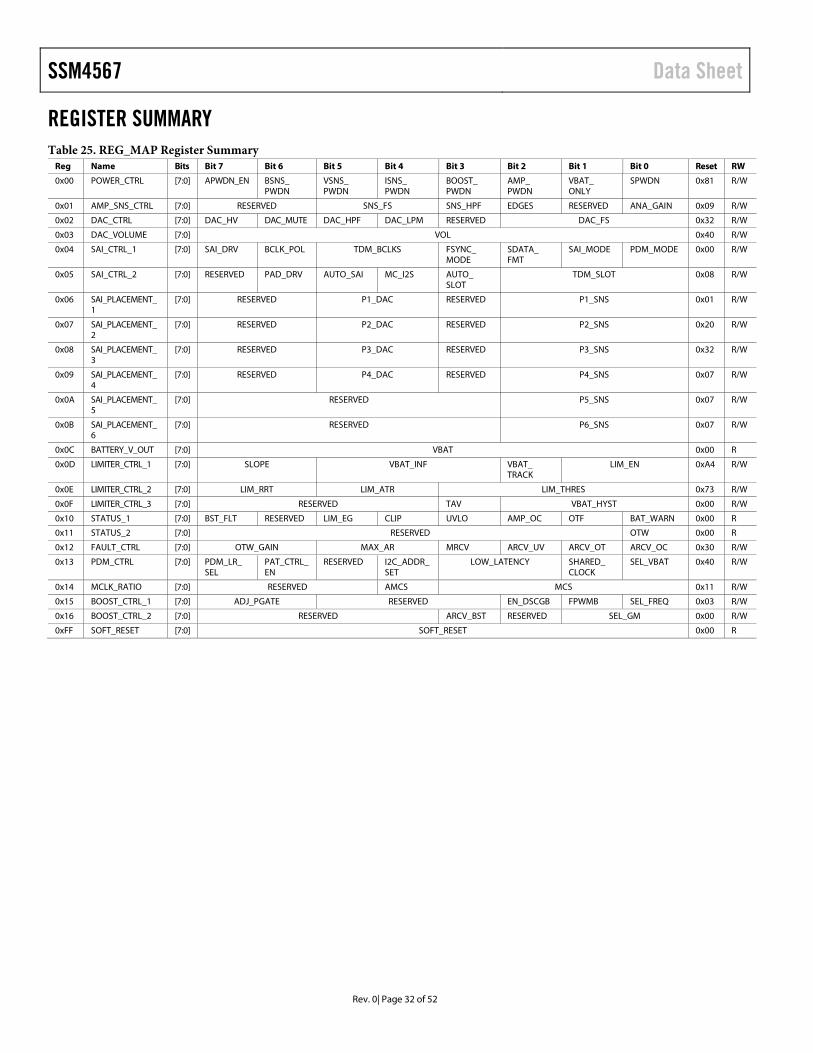
SSM4567 Data Sheet
Rev. 0| Page 32 of 52
REGISTER SUMMARY Table 25. REG_MAP Register Summary
Reg Name Bits Bit 7 Bit 6 Bit 5 Bit 4 Bit 3 Bit 2 Bit 1 Bit 0 Reset RW 0x00 POWER_CTRL [7:0] APWDN_EN BSNS_
PWDN VSNS_ PWDN
ISNS_ PWDN
BOOST_ PWDN
AMP_ PWDN
VBAT_ ONLY
SPWDN 0x81 R/W
0x01 AMP_SNS_CTRL [7:0] RESERVED SNS_FS SNS_HPF EDGES RESERVED ANA_GAIN 0x09 R/W 0x02 DAC_CTRL [7:0] DAC_HV DAC_MUTE DAC_HPF DAC_LPM RESERVED DAC_FS 0x32 R/W 0x03 DAC_VOLUME [7:0] VOL 0x40 R/W 0x04 SAI_CTRL_1 [7:0] SAI_DRV BCLK_POL TDM_BCLKS FSYNC_
MODE SDATA_ FMT
SAI_MODE PDM_MODE 0x00 R/W
0x05 SAI_CTRL_2 [7:0] RESERVED PAD_DRV AUTO_SAI MC_I2S AUTO_ SLOT
TDM_SLOT 0x08 R/W
0x06 SAI_PLACEMENT_1
[7:0] RESERVED P1_DAC RESERVED P1_SNS 0x01 R/W
0x07 SAI_PLACEMENT_2
[7:0] RESERVED P2_DAC RESERVED P2_SNS 0x20 R/W
0x08 SAI_PLACEMENT_3
[7:0] RESERVED P3_DAC RESERVED P3_SNS 0x32 R/W
0x09 SAI_PLACEMENT_4
[7:0] RESERVED P4_DAC RESERVED P4_SNS 0x07 R/W
0x0A SAI_PLACEMENT_5
[7:0] RESERVED P5_SNS 0x07 R/W
0x0B SAI_PLACEMENT_6
[7:0] RESERVED P6_SNS 0x07 R/W
0x0C BATTERY_V_OUT [7:0] VBAT 0x00 R 0x0D LIMITER_CTRL_1 [7:0] SLOPE VBAT_INF VBAT_
TRACK LIM_EN 0xA4 R/W
0x0E LIMITER_CTRL_2 [7:0] LIM_RRT LIM_ATR LIM_THRES 0x73 R/W 0x0F LIMITER_CTRL_3 [7:0] RESERVED TAV VBAT_HYST 0x00 R/W 0x10 STATUS_1 [7:0] BST_FLT RESERVED LIM_EG CLIP UVLO AMP_OC OTF BAT_WARN 0x00 R 0x11 STATUS_2 [7:0] RESERVED OTW 0x00 R 0x12 FAULT_CTRL [7:0] OTW_GAIN MAX_AR MRCV ARCV_UV ARCV_OT ARCV_OC 0x30 R/W 0x13 PDM_CTRL [7:0] PDM_LR_
SEL PAT_CTRL_EN
RESERVED I2C_ADDR_SET
LOW_LATENCY SHARED_ CLOCK
SEL_VBAT 0x40 R/W
0x14 MCLK_RATIO [7:0] RESERVED AMCS MCS 0x11 R/W 0x15 BOOST_CTRL_1 [7:0] ADJ_PGATE RESERVED EN_DSCGB FPWMB SEL_FREQ 0x03 R/W 0x16 BOOST_CTRL_2 [7:0] RESERVED ARCV_BST RESERVED SEL_GM 0x00 R/W 0xFF SOFT_RESET [7:0] SOFT_RESET 0x00 R

Data Sheet SSM4567
Rev. 0| Page 33 of 52
REGISTER DETAILS POWER CONTROL REGISTER Address: 0x00, Reset: 0x81, Name: POWER_CTRL
Table 26. Bit Descriptions for POWER_CTRL Bits Bit Name Settings Description Reset Access 7 APWDN_EN Auto Power-Down Enable. Auto power down automatically puts the IC in a low
power state when 2048 consecutive zero input samples have been received. 0x1 R/W
0 Auto Power-Down Disabled. 1 Auto Power-Down Enabled When APWDN_EN=1. The device automatically powers
down when 2048 consecutive zero value input samples have been received. The device automatically powers up when a single non zero sample is received.
6 BSNS_PWDN Battery Voltage Sense Power Down. 0x0 R/W 0 Battery Voltage Sense Powered On. 1 Battery Voltage Sense Powered Off. 5 VSNS_PWDN Voltage Sense Power-Down. 0x0 R/W 0 Voltage Sense Powered On. 1 Voltage Sense Powered Off. 4 ISNS_PWDN Current Sense Power Down. 0x0 R/W 0 Current Sense Powered On. 1 Current Sense Powered Off. 3 BOOST_PWDN Boost Converter Power-Down. When the boost converter is powered down, the
Class-D operates directly from VBAT power supply. 0x0 R/W
0 Boost Converter Enabled. 1 Boost Converter Powered Down. 2 AMP_PWDN Amplifier Power-Down. 0x0 R/W 0 Amplifier and DAC Normal Operation. 1 Amplifier and DAC Powered Down. 1 VBAT_ONLY Class-D Power Switch. 0x0 R/W 0 Class-D can switch between VBAT and PVDD as a five-level output. 1 Class-D powered from VBAT only, even if the booster is on. 0 SPWDN Master Software Power-Down. Software power-down puts all blocks except the I2C
interface in a low power state. 0x1 R/W
0 Normal Operation. 1 Software Master Power-Down.

SSM4567 Data Sheet
Rev. 0| Page 34 of 52
AMP AND SENSE CONTROL REGISTER Address: 0x01, Reset: 0x09, Name: AMP_SNS_CTRL
Table 27. Bit Descriptions for AMP_SNS_CTRL Bits Bit Name Settings Description Reset Access [7:6] RESERVED Reserved. 0x0 R/W [5:4] SNS_FS Sense Sample Rate. The sense output sample rate can be set at a lower rate than the
DAC. 0x0 R/W
00 Sense Sample Rate same as the DAC. 01 Sense Sample Rate 1/2 of the DAC. 10 Sense Sample Rate 1/4 of the DAC. 11 Sense Sample Rate 1/8 of the DAC. 3 SNS_HPF SNS High Pass Filter Enable. 0x1 R/W 0 SNS High Pass Filter Off. 1 SNS High Pass Filter On . 2 EDGES Edge Rate Control. This controls the edge speed of the power stage. The low EMI
operation mode reduces the edge speed, lowering EMI and power efficiency. 0x0 R/W
0 Normal Operation. 1 Low EMI Mode Operation for Class-D power stage. 1 RESERVED Reserved. 0x0 R/W 0 ANA_GAIN Amplifier Analog Gain Selection. 0x1 R/W 0 3.6 V Full-Scale Gain Mapping. 1 5.2 V Full-Scale Gain Mapping.

Data Sheet SSM4567
Rev. 0| Page 35 of 52
DAC CONTROL REGISTER Address: 0x02, Reset: 0x32, Name: DAC_CTRL
Table 28. Bit Descriptions for DAC_CTRL Bits Bit Name Settings Description Reset Access 7 DAC_HV DAC Hard Volume 0x0 R/W 0 Soft Volume Ramping 1 Hard/Immediate Volume Change 6 DAC_MUTE DAC Mute Control 0x0 R/W 0 DAC Unmuted 1 DAC Muted 5 DAC_HPF DAC High-Pass Filter Enable 0x1 R/W 0 DAC High-Pass Filter Off 1 DAC High-Pass Filter On 4 DAC_LPM DAC Low Power Mode Enable 0x1 R/W 0 DAC Low Power Mode Off (128 × fs in PDM Mode) 1 DAC Low Power Mode On (64 × fs in PDM Mode) 3 RESERVED Reserved. 0x0 R/W [2:0] DAC_FS DAC Sample Rate Selection 0x2 R/W 000 8 kHz to 12 kHz Sample Rate 001 16 kHz to 24 kHz Sample Rate 010 32 kHz to 48 kHz Sample Rate 011 64 kHz to 96 kHz Sample Rate 100 128 kHz to 192 kHz Sample Rate 101 Reserved 110 Reserved 111 Reserved

SSM4567 Data Sheet
Rev. 0| Page 36 of 52
DAC VOLUME CONTROL REGISTER Address: 0x03, Reset: 0x40, Name: DAC_VOLUME
Table 29. Bit Descriptions for DAC_VOLUME Bits Bit Name Settings Description Reset Access [7:0] VOL Volume Control 0x40 R/W 00000000 +24 dB 00000001 +23.625 dB 00000010 +23.35 dB 00000011 +22.875 dB 00000100 +22.5 dB 00000101 ... 00111111 +0.375 dB 01000000 0 01000001 -0.375 dB 01000010 ... 11111101 −70.875 dB 11111110 −71.25 dB 11111111 Mute

Data Sheet SSM4567
Rev. 0| Page 37 of 52
SERIAL AUDIO INTERFACE CONTROL 1 REGISTER Address: 0x04, Reset: 0x00, Name: SAI_CTRL_1
Table 30. Bit Descriptions for SAI_CTRL_1 Bits Bit Name Settings Description Reset Access 7 SAI_DRV Drive Control for Unused BCLK Cycles 0x0 R/W 0 Unused BCLK cycles on SNS_SDATA are not driven (high-Z) 1 Unused BCLK cycles on SNS_SDATA are driven low 6 BCLK_POL BCLK Polarity 0x0 R/W 0 Rising Edge of BCLK is used to register SDATA 1 Falling Edge of BCLK is used to register SDATA [5:4] TDM_BCLKS Number of BCLK cycles per chip in TDM Mode. Any number of BCLK cycles per
FSYNC can be used in stereo modes (I2S/left justified) or in TDM mode with only one chip. When in TDM mode, with multiple chips on the TDM bus, the number of BCLK cycles per chip must be defined.
0x0 R/W
00 32 BCLK cycles per chip in TDM 01 48 BCLK cycles per chip in TDM 10 64 BCLK cycles per chip in TDM 11 64 BCLK cycles per chip in TDM 3 FSYNC_MODE FSYNC Mode Control 0x0 R/W 0 Low FSYNC is Left Channel in Stereo Modes or Pulsed FSYNC Mode in TDM Modes 1 High FSYNC is Left Channel in Stereo Modes or 50% FSYNC Mode in TDM Modes 2 SDATA_FMT Serial Data Format 0x0 R/W 0 I2S/Delay by one from FSYNC edge 1 Left Justified/No delay from FSYNC edge 1 SAI_MODE Serial Audio Interface Mode Selection 0x0 R/W 0 Stereo Modes (I2S, left justified) 1 TDM/PCM Modes 0 PDM_MODE PDM Input and Output Mode 0x0 R/W 0 Normal Serial Audio Interface Operation 1 PDM used for input and output

SSM4567 Data Sheet
Rev. 0| Page 38 of 52
SERIAL AUDIO INTERFACE CONTROL 2 REGISTER Address: 0x05, Reset: 0x08, Name: SAI_CTRL_2
Table 31. Bit Descriptions for SAI_CTRL_2 Bits Bit Name Settings Description Reset Access 7 RESERVED Reserved. 0x0 R/W 6 PAD_DRV Output pad drive strength control. SNS_PDM_DAT/SNS_SDATAO pin output drive
strength. 0x0 R/W
0 low strength 1 high strength 5 AUTO_SAI Automatic Serial Audio Interface Detection Enable. When AUTO_SAI = 1 the Serial
Audio Interface automatically configures based on the connections of BCLK and FSYNC. When FSYNC and BCLK are connected normally, and a pulsed FSYNC is detected, the interface automatically configures for TDM operation. When FSYNC and BCLK are connected normally, and a 50% duty cycle FSYNC is detected, the interface automatically configures for multichip I2S operation. When FSYNC and BCLK are connected to the opposite pins, the interface automatically configures for normal I2S operation. When set for automatic detection the values of SAI_MODE and SDATA_FMT are ignored.
0x0 R/W
0 SAI_MODE, SDATA_FMT, and MC_I2S are used to set the Serial Audio Interface configuration
1 Auto Serial Audio Interface Detection Enabled 4 MC_I2S Multichip I2S Enable. When MC_I2S is selected, this overrides the SAI_MODE selection. 0x0 R/W 0 Normal Operation 1 Multichip I2S Operation 3 AUTO_SLOT Automatic TDM and MC I2S slot selection 0x1 R/W 0 TDM/MC I2S Slot determined by TDM_SLOT bits 1 TDM/MC I2S Slot determined by ADDR pin [2:0] TDM_SLOT TDM and Multichip I2S slot selection 0x0 R/W 000 Chip Slot 1 Used 001 Chip Slot 2 Used 010 Chip Slot 3 Used 011 Chip Slot 4 Used 100 Chip Slot 5 Used 101 Chip Slot 6 Used 110 Chip Slot 7 Used 111 Chip Slot 8 Used

Data Sheet SSM4567
Rev. 0| Page 39 of 52
SERIAL AUDIO INTERFACE PLACEMENT 1 CONTROL REGISTER Address: 0x06, Reset: 0x01, Name: SAI_PLACEMENT_1
Table 32. Bit Descriptions for SAI_PLACEMENT_1 Bits Bit Name Settings Description Reset Access [7:6] RESERVED Reserved. 0x0 R/W [5:4] P1_DAC Placement 1 or L1 (Left 1) Control for DAC Input. Selects the size of the data to be read.
24 bits or 16 bits. This slot can also be set to read in eight bits, throw them away, and move on to Placement P2 to read the audio data.
0x0 R/W
00 24-Bit DAC Input 01 16-Bit DAC Input 10 Read and Ignore 8-bits 11 Read and Ignore 8-bits 3 RESERVED Reserved. 0x0 R/W [2:0] P1_SNS Placement 1 or L1 (Left 1) Control for Sense Output. 0x1 R/W 000 16-Bit Voltage Output 001 16-Bit Current Output 010 8-Bit Battery Voltage Output Unsigned 011 8-Bit Control Data Output 100 Alternating 16-Bit Voltage and Current 101 8-Bit Status Output 110 8-Bit V/I Marker and Slot ID 111 Blank 8 Bits

SSM4567 Data Sheet
Rev. 0| Page 40 of 52
SERIAL AUDIO INTERFACE PLACEMENT 2 CONTROL REGISTER Address: 0x07, Reset: 0x20, Name: SAI_PLACEMENT_2
Table 33. Bit Descriptions for SAI_PLACEMENT_2 Bits Bit Name Settings Description Reset Access [7:6] RESERVED Reserved. 0x0 R/W [5:4] P2_DAC Placement 2 or R1 (Right 1) Control for DAC Input. Selects the size of the data to be
read. 24 bits or 16 bits. This slot can also be set to read in eight bits, throw them away, and move on to Placement P3 to read the audio data.
0x2 R/W
00 24-Bit DAC Input 01 16-Bit DAC Input 10 Read and Ignore 8 bits 11 Read and Ignore 8 bits 3 RESERVED Reserved. 0x0 R/W [2:0] P2_SNS Placement 2 or R1 (Right 1) Control for Sense Output. 0x0 R/W 000 16-Bit Voltage Output 001 16-Bit Current Output 010 8-Bit Battery Voltage Output Unsigned 011 8-Bit Control Data Output 100 Alternating 16-Bit Voltage and Current 101 8-Bit Status Output 110 8-Bit V/I Marker and Slot ID 111 Blank 8 Bits

Data Sheet SSM4567
Rev. 0| Page 41 of 52
SERIAL AUDIO INTERFACE PLACEMENT 3 CONTROL REGISTER Address: 0x08, Reset: 0x32, Name: SAI_PLACEMENT_3
Table 34. Bit Descriptions for SAI_PLACEMENT_3 Bits Bit Name Settings Description Reset Access [7:6] RESERVED Reserved. 0x0 R/W [5:4] P3_DAC Placement 3 or L2 (Left 2) Control for DAC Input. Selects the size of the data to be read.
24 bits or 16 bits. This slot can also be set to read in eight bits, throw them away, and move on to placement P4 to read the audio data.
0x3 R/W
00 24-Bit DAC Input 01 16-Bit DAC Input 10 Read and Ignore 8 bits 11 Read and Ignore 8 bits 3 RESERVED Reserved. 0x0 R/W [2:0] P3_SNS Placement 3 or L2 (Left 2) Control for Sense Output. 0x2 R/W 000 16-Bit Voltage Output 001 16-Bit Current Output 010 8-Bit Battery Voltage Output Unsigned 011 8-Bit Control Data Output 100 Alternating 16-Bit Voltage and Current 101 8-Bit Status Output 110 8-Bit V/I Marker and Slot ID 111 Blank 8 Bits

SSM4567 Data Sheet
Rev. 0| Page 42 of 52
SERIAL AUDIO INTERFACE PLACEMENT 4 CONTROL REGISTER Address: 0x09, Reset: 0x07, Name: SAI_PLACEMENT_4
Table 35. Bit Descriptions for SAI_PLACEMENT_4 Bits Bit Name Settings Description Reset Access [7:6] RESERVED Reserved. 0x0 R/W [5:4] P4_DAC Placement 4 or R2 (Right 2) Control for DAC Input 0x0 R/W 00 24-Bit DAC Input 01 16-Bit DAC Input 10 Read and Ignore 8 bits 11 Read and Ignore 8 bits 3 RESERVED Reserved. 0x0 R/W [2:0] P4_SNS Placement 4 or R2 (Right 2) Control for Sense Output 0x7 R/W 000 16-Bit Voltage Output 001 16-Bit Current Output 010 8-Bit Battery Voltage Output Unsigned 011 8-Bit Control Data Output 100 Alternating 16-Bit Voltage and Current 101 8-Bit Status Output 110 8-Bit V/I Marker and Slot ID 111 Blank 8 Bits

Data Sheet SSM4567
Rev. 0| Page 43 of 52
SERIAL AUDIO INTERFACE PLACEMENT 5 CONTROL REGISTER Address: 0x0A, Reset: 0x07, Name: SAI_PLACEMENT_5
Table 36. Bit Descriptions for SAI_PLACEMENT_5 Bits Bit Name Settings Description Reset Access [7:3] RESERVED Reserved. 0x0 R/W [2:0] P5_SNS Placement 5 or L3 (Left 3) Control for Sense Output 0x7 R/W 000 16-Bit Voltage Output 001 16-Bit Current Output 010 8-Bit Battery Voltage Output Unsigned 011 8-Bit Control Data Output 100 Alternating 16-Bit Voltage and Current 101 8-Bit Status Output 110 8-Bit V/I Marker and Slot ID 111 Blank 8 Bits
SERIAL AUDIO INTERFACE PLACEMENT 6 CONTROL REGISTER Address: 0x0B, Reset: 0x07, Name: SAI_PLACEMENT_6
Table 37. Bit Descriptions for SAI_PLACEMENT_6 Bits Bit Name Settings Description Reset Access [7:3] RESERVED Reserved. 0x0 R/W [2:0] P6_SNS Placement 6 or R3 (Right 3) Control for Sense Output 0x7 R/W 000 16-Bit Voltage Output 001 16-Bit Current Output 010 8-Bit Battery Voltage Output Unsigned 011 8-Bit Control Data Output 100 Alternating 16-Bit Voltage and Current 101 8-Bit Status Output 110 8-Bit V/I Marker and Slot ID 111 Blank 8 Bits

SSM4567 Data Sheet
Rev. 0| Page 44 of 52
BATTERY VOLTAGE OUTPUT REGISTER Address: 0x0C, Reset: 0x00, Name: BATTERY_V_OUT
Table 38. Bit Descriptions for BATTERY_V_OUT Bits Bit Name Settings Description Reset Access [7:0] VBAT 8-Bit Unsigned Battery Voltage 0x0 R
LIMITER CONTROL 1 REGISTER Address: 0x0D, Reset: 0xA4, Name: LIMITER_CTRL_1
Table 39. Bit Descriptions for LIMITER_CTRL_1 Bits Bit Name Settings Description Reset Access [7:6] SLOPE Limiter Ratio below the VBAT_INF threshold. Limiter ratio once the VBAT voltage falls
below the VBAT_INF threshold. This sets the slope of the limiter curve as the VBAT voltage falls.
0x2 R/W
00 1:1 Limiter Ratio 01 2:1 Limiter Ratio 10 3:1 Limiter Ratio 11 4:1 Limiter Ratio [5:3] VBAT_INF Battery Voltage Inflection point. When VBAT drops below the inflection point and
VBAT_TRACK = 1 the limiter threshold starts being lowered to limit maximum output and peak current from the battery. The amount of reduction when the battery voltage is lower than VBAT_INF is determined by the SLOPE bits.
0x4 R/W
000 3.9 V 001 3.8 V 010 3.7 V 011 3.6 V 100 3.5 V 101 3.4 V 110 3.3 V 111 3.2 V 2 VBAT_TRACK Threshold Battery Tracking Enable 0x1 R/W 0 Limiter Attack Threshold Fixed 1 Limiter Attack Threshold Varies or gain reduction with Battery Voltage [1:0] LIM_EN Limiter or Mute mode Enable 0x0 R/W 00 Limiter and mute mode Off 01 Limiter On 10 Output will mute if VBAT is below VBAT_INF 11 Limiter On but will only engage if VBAT is below VBAT_INF

Data Sheet SSM4567
Rev. 0| Page 45 of 52
LIMITER CONTROL 2 REGISTER Address: 0x0E, Reset: 0x73, Name: LIMITER_CTRL_2
Table 40. Bit Descriptions for LIMITER_CTRL_2 Bits Bit Name Settings Description Reset Access [7:6] LIM_RRT Limiter Release Rate 0x1 R/W 00 3200 ms/dB 01 1600 ms/dB 10 1200 ms/dB 11 800 ms/dB [5:4] LIM_ATR Limiter Attack Rate 0x3 R/W 00 120 μs/dB 01 60 μs/dB 10 30 μs/dB 11 20 μs/dB [3:0] LIM_THRES Limiter Attack Threshold 0x3 R/W 0000 6.6 V peak Output 0001 6.4 V peak Output 0010 6.2 V peak Output 0011 6.0 V peak Output 0100 5.8 V peak Output 0101 5.6 V peak Output 0110 5.4 V peak Output 0111 5.2 V peak Output 1000 5.0 V peak Output 1001 4.8 V peak Output 1010 4.6 V peak Output 1011 4.4 V peak Output 1100 4.2 V peak Output 1101 4.0 V peak Output 1110 3.8 V peak Output 1111 3.6 V peak Output

SSM4567 Data Sheet
Rev. 0| Page 46 of 52
LIMITER CONTROL 3 REGISTER Address: 0x0F, Reset: 0x00, Name: LIMITER_CTRL_3
Table 41. Bit Descriptions for LIMITER_CTRL_3 Bits Bit Name Settings Description Reset Access [7:4] RESERVED Reserved. 0x0 R/W 3 TAV TAV, Detector Time Averaging Filter 0x0 R/W 0 Long RMS average time 1 Short RMS average time [2:0] VBAT_HYST vbat_hyst 0x0 R/W 000 No hysteresis 001 −36 dBV 010 −33 dBV 011 −30 dBV 100 −27 dBV 101 −24 dBV 110 −21 dBV 111 −18 dBV

Data Sheet SSM4567
Rev. 0| Page 47 of 52
STATUS 1 REGISTER Address: 0x10, Reset: 0x00, Name: STATUS_1
Table 42. Bit Descriptions for STATUS_1 Bits Bit Name Settings Description Reset Access 7 BST_FLT Boost Fault Status 0x0 R 0 Normal Operation 1 Boost Converter Fault Condition 6 RESERVED Reserved. 0x0 R 5 LIM_EG Limiter/Gain Reduction Engaged 0x0 R 0 Normal Operation 1 Limiter or Gain Reduction has Reduced Gain 4 CLIP Clip Detector 0x0 R 0 Normal Operation 1 Amplifier Clipping Detected 3 UVLO Under Voltage Fault Status 0x0 R 0 Normal Operation 1 Under Voltage Fault 2 AMP_OC Amplifier Overcurrent Fault Status 0x0 R 0 Normal Operation 1 Amp Overcurrent Fault Condition 1 OTF Over Temperature Fault Status 0x0 R 0 Normal Operation 1 Over Temperature Fault Condition 0 BAT_WARN Battery Voltage Warning 0x0 R 0 Battery Voltage above VBAT_INF 1 Battery Voltage at or below VBAT_INF
STATUS 2 REGISTER Address: 0x11, Reset: 0x00, Name: STATUS_2
Table 43. Bit Descriptions for STATUS_2 Bits Bit Name Settings Description Reset Access [7:1] RESERVED Reserved. 0x0 R 0 OTW Overtemperature Warning Status 0x0 R 0 Normal Operation 1 Overtemperature Warning Condition

SSM4567 Data Sheet
Rev. 0| Page 48 of 52
FAULT CONTROL REGISTER Address: 0x12, Reset: 0x30, Name: FAULT_CTRL
Table 44. Bit Descriptions for FAULT_CTRL Bits Bit Name Settings Description Reset Access [7:6] OTW_GAIN Over Thermal Warning Gain Reduction 0x0 R/W 00 No gain reduction in thermal warning 01 1.5 dB gain reduction in thermal warning 10 3 dB gain reduction in thermal warning 11 5.625 dB gain reduction in thermal warning [5:4] MAX_AR Maximum Fault recovery Attempts. The Maximum autorecovery register determines
how many attempts at auto recovery are performed. 0x3 R/W
00 1 Autorecovery Attempt 01 3 Autorecovery Attempts 10 7 Autorecovery Attempts 11 Unlimited Autorecovery Attempts 3 MRCV Manual Fault Recovery 0x0 W 0 Normal Operation 1 Writing of 1 causes a manual fault recovery attempt when
ARCV_OC/ARCV_OT/ARCV_UV/ARCV_BST = 1
2 ARCV_UV Undervoltage Autofault Recovery Control 0x0 R/W 0 Auto Fault Recovery for Undervoltage Fault 1 Manual Fault Recovery for Undervoltage Fault 1 ARCV_OT Overtemperature Auto Fault Recovery Control 0x0 R/W 0 Auto Fault Recovery for Overtemperature Fault 1 Manual Fault Recovery for Overtemperature Fault 0 ARCV_OC Overcurrent Auto Fault Recovery Control 0x0 R/W 0 Auto Fault Recovery for Overcurrent Fault 1 Manual Fault Recovery for Overcurrent Fault

Data Sheet SSM4567
Rev. 0| Page 49 of 52
PDM CONTROL REGISTER Address: 0x13, Reset: 0x40, Name: PDM_CTRL
Table 45. Bit Descriptions for PDM_CTRL Bits Bit Name Settings Description Reset Access 7 PDM_LR_SEL PDM left/right channel select when external PIN SEL =1 0x0 R/W 0 select left channel 1 select right channel 6 PAT_CTRL_EN Enable PDM pattern control when external PIN SEL=0 0x1 R/W 0 Disable PDM pattern control 1 Enable PDM pattern control 5 RESERVED Reserved. 0x0 R/W 4 I2C_ADDR_SET Setting the I2C Address in PDM mode when external PIN SEL = 0 0x0 R/W 0 I2C Address is fixed to 0x34 in PDM mode 1 I2C Address determined by LR_SEL/ADDR pin in PDM mode (LR_SEL/ADDR = 0,
Address = 0x34; LR_SEL/ADDR = 1, Address = 0x35)
[3:2] LOW_LATENCY Low latency Mode 0x0 R/W 00 Normal Mode 01 Low latency Mode, delay about 15 µs 10 Low latency Mode, delay about 5 µs 1 SHARED_CLOCK Only DAC_PDM_CLK is needed 0x0 R/W 0 Do not share 1 DAC_PDM_CLK is shared with SNS_PDM_CLK 0 SEL_VBAT Select VBAT to output 0x0 R/W 0 output sense voltage in PDM mode 1 Output sense battery voltage (VBAT) in PDM mode
MCLK RATIO SETTING REGISTER Address: 0x14, Reset: 0x11, Name: MCLK_RATIO
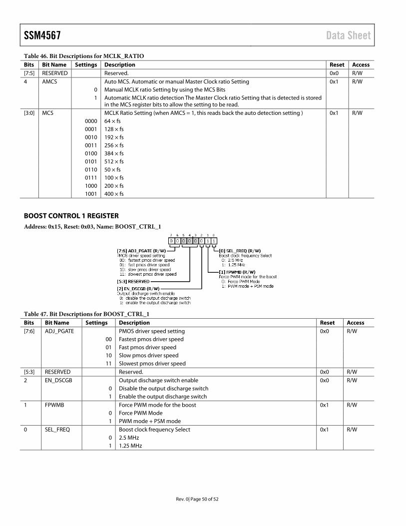
SSM4567 Data Sheet
Rev. 0| Page 50 of 52
Table 46. Bit Descriptions for MCLK_RATIO Bits Bit Name Settings Description Reset Access [7:5] RESERVED Reserved. 0x0 R/W 4 AMCS Auto MCS. Automatic or manual Master Clock ratio Setting 0x1 R/W 0 Manual MCLK ratio Setting by using the MCS Bits 1 Automatic MCLK ratio detection The Master Clock ratio Setting that is detected is stored
in the MCS register bits to allow the setting to be read.
[3:0] MCS MCLK Ratio Setting (when AMCS = 1, this reads back the auto detection setting ) 0x1 R/W 0000 64 × fs 0001 128 × fs 0010 192 × fs 0011 256 × fs 0100 384 × fs 0101 512 × fs 0110 50 × fs 0111 100 × fs 1000 200 × fs 1001 400 × fs
BOOST CONTROL 1 REGISTER Address: 0x15, Reset: 0x03, Name: BOOST_CTRL_1
Table 47. Bit Descriptions for BOOST_CTRL_1 Bits Bit Name Settings Description Reset Access [7:6] ADJ_PGATE PMOS driver speed setting 0x0 R/W 00 Fastest pmos driver speed 01 Fast pmos driver speed 10 Slow pmos driver speed 11 Slowest pmos driver speed [5:3] RESERVED Reserved. 0x0 R/W 2 EN_DSCGB Output discharge switch enable 0x0 R/W 0 Disable the output discharge switch 1 Enable the output discharge switch 1 FPWMB Force PWM mode for the boost 0x1 R/W 0 Force PWM Mode 1 PWM mode + PSM mode 0 SEL_FREQ Boost clock frequency Select 0x1 R/W 0 2.5 MHz 1 1.25 MHz

Data Sheet SSM4567
Rev. 0| Page 51 of 52
BOOST CONTROL 2 REGISTER Address: 0x16, Reset: 0x00, Name: BOOST_CTRL_2
Table 48. Bit Descriptions for BOOST_CTRL_2 Bits Bit Name Settings Description Reset Access [7:4] RESERVED Reserved 0x0 R/W 3 ARCV_BST Autorecovery setting for boost fault 0x0 R/W 0 Autorecovery for boost fault 1 Manual recovery for boost fault 2 RESERVED Reserved 0x0 R/W [1:0] SEL_GM Transconductance (gm) selection for the error amplifier in the boost 0x0 R/W 00 12.5 μS gm 01 16.6 μS gm 10 20.0 μS gm 11 25.0 μS gm
SOFT RESET REGISTER Address: 0xFF, Reset: 0x00, Name: SOFT_RESET
Table 49. Bit Descriptions for SOFT_RESET Bits Bit Name Settings Description Reset Access [7:0] SOFT_RESET Soft Reset (write the value 0x00 to this register to initiate a soft reset) 0x0 R

SSM4567 Data Sheet
Rev. 0| Page 52 of 52
OUTLINE DIMENSIONS
Figure 58. 19-Ball Wafer Level Chip Scale Package [WLCSP]
(CB-19-1) Dimensions shown in millimeters
ORDERING GUIDE Model1 Temperature Range Package Description Package Option SSM4567ACBZ-R7 −40°C to +85°C 19-Ball WLCSP CB-19-1 SSM4567ACBZ-RL −40°C to +85°C 19-Ball WLCSP CB-19-1 EVAL-SSM4567Z Evaluation Board EVAL-SSM4567MINIZ Evaluation Board 1 Z = RoHS Compliant Part.
I2C refers to a communications protocol originally developed by Philips Semiconductors (now NXP Semiconductors).
A
B
C
D
E
2.1402.1002.060
1.7801.7401.700
1234
BOTTOM VIEW(BALL SIDE UP)
TOP VIEW(BALL SIDE DOWN)
BALL A1IDENTIFIER
0.40BSC
0.5600.5000.440
SIDE VIEW
0.2300.2000.170
0.3000.2600.220
1.60 REF
1.20 REF
COPLANARITY0.05
SEATINGPLANE
12-1
9-2
01
2-A
©2014 Analog Devices, Inc. All rights reserved. Trademarks and registered trademarks are the property of their respective owners. D12278-0-4/14(0)


![POWER AMPLIFIER KAC-7204 - ePanorama · KAC-7204 POWER AMPLIFIER Stereo/Bridgeable Power Amplifier BASS BOOST LEVEL[dB] LPF FREQUENCY[Hz] HPF FREQUENCY[Hz] INPUT SENSITIVITY[V] [MIN]](https://img.dokumen.tips/doc/110x75/5f0714757e708231d41b33c5/power-amplifier-kac-7204-epanorama-kac-7204-power-amplifier-stereobridgeable.jpg)