Embed Size (px)
Citation preview

OUT-
OUT+
VBOOST
SW
Ferrite bead(optional)
VREG
VSENSE-
VSENSE+
Ferrite bead(optional)
To Speaker
+
-
/RESET
I2S
4
2
I2C
C12VBAT
MCLK
TAS2555
C2
L1
2
Product
Folder
Order
Now
Technical
Documents
Tools &
Software
Support &Community
An IMPORTANT NOTICE at the end of this data sheet addresses availability, warranty, changes, use in safety-critical applications,intellectual property matters and other important disclaimers. PRODUCTION DATA.
TAS2555SLASE69A –AUGUST 2015–REVISED NOVEMBER 2016
TAS2555 5.7-W Class-D Mono Audio Amplifier with Class-H Boost and Speaker Sense
1
1 Features1• Ultra Low-Noise Mono Boosted Class-D Amplifier
– 5.7 W at 1% THD+N and 6.9 W at 10%THD+N into 4-Ω Load from 4.2-V Supply
– 3.8 W at 1% THD+N and 4.5 W at 10%THD+N into 8-Ω Load from 4.2-V Supply
• Output Noise for DAC + Class-D (ICN) is 15.9 µV• DAC + Class-D SNR 111 dB at 1%THD+N/8 Ω• THD+N –90 dB at 1 W / 8 Ω with Flat Frequency
Response• PSRR 110 dB for 200 mVpp ripple at 217 Hz• Input Sample Rates from 8 kHz to 96 kHz• Built-In Speaker Sense
– Measures Speaker Current and Voltage– Measures VBAT Voltage, Chip Temperature
• Dedicated Real-Time DSP for Speaker Protection– Thermal and Excursion Protection– Detects Speaker Leaks and Damage
• High Efficiency Class-H Boost Converter WithMulti-Level Tracking– 86% at 500 mW in 8 Ω with 3.6 V VBAT
– 87% at 700 mW in 8 Ω with 4.2 V VBAT
• Configurable Automatic Gain Control (AGC)– Limits Battery Current Consumption
• Adjustable Class-D Switching Edge-Rate Control• Thermal, Short-Circuit, and Under-Voltage
Protection• I2S, Left-Justified, Right-Justified, DSP, and TDM
Input and Output Interface,• I2C or SPI Interface for Register Control• Stereo Configuration Using Two TAS2555
Devices• Power Supplies
– Boost Input: 2.9 V to 5.5 V– Analog/Digital: 1.65 V to 1.95 V– Digital I/O: 1.62 V to 3.6 V
• 42-ball, 0.5-mm pitch, DSBGA package
2 Applications• Mobile Phones & Tablets• Video Doorbells & Voice Enabled Thermostats• Personal Computers• Bluetooth Speakers and Accessories
3 DescriptionThe TAS2555 device is a state-of-the-art Class-Daudio amplifier which is a full system on a Chip(SoC). The device features a ultra low-noise audioDAC and Class-D power amplifier which incorporatesspeaker voltage and current sensing feedback. Anon-chip, low-latency DSP supports Texas InstrumentsSmartAmp speaker protection algorithms tomaximizes loudness while maintaining safe speakerconditions.
The device can be used easily with any processorwith an I2S output and stereo implementations arepossible when using two TAS2555 devices. Separatetuning for different speakers is supported allowingcustomers to add value while maintaining form factordesigns. Additionally, the TAS2555 supports separatevoice and audio tuning dynamically with ultra-low 15.9µV ICN regardless of mode of operation makingreceiver/speaker implementations possible.
A Class-H boost converter generates the Class-Damplifier supply rail. When the audio signal onlyrequires a lower Class-D output power, the boostimproves system efficiency by deactivating andconnecting VBAT directly to the Class-D amplifiersupply. When higher audio output power is required,the multi-level boost quickly activates tracking thesignal to provide the additional voltage to the load.
Device Information(1)
PART NUMBER PACKAGE BODY SIZE (NOM)TAS2555 DSBGA (42) 3.47 mm × 3.23 mm
(1) For all available packages, see the orderable addendum atthe end of the data sheet.
Simplified Schematic

2
TAS2555SLASE69A –AUGUST 2015–REVISED NOVEMBER 2016 www.ti.com
Product Folder Links: TAS2555
Submit Documentation Feedback Copyright © 2015–2016, Texas Instruments Incorporated
Table of Contents1 Features .................................................................. 12 Applications ........................................................... 13 Description ............................................................. 14 Revision History..................................................... 25 Device Comparison Table ..................................... 36 Pin Configuration and Functions ......................... 47 Specifications......................................................... 6
7.1 Absolute Maximum Ratings ...................................... 67.2 ESD Ratings.............................................................. 67.3 Recommended Operating Conditions....................... 67.4 Thermal Information .................................................. 67.5 Electrical Characteristics........................................... 77.6 I2C Timing Requirements ......................................... 97.7 SPI Timing Requirements ........................................ 97.8 I2S/LJF/RJF Timing in Master Mode ...................... 107.9 I2S/LJF/RJF Timing in Slave Mode ........................ 107.10 DSP Timing in Master Mode ................................ 107.11 DSP Timing in Slave Mode .................................. 117.12 Typical Characteristics .......................................... 14
8 Parameter Measurement Information ................ 169 Detailed Description ............................................ 17
9.1 Overview ................................................................. 179.2 Functional Block Diagram ....................................... 189.3 Feature Description................................................. 189.4 Device Functional Modes........................................ 24
9.5 Programming........................................................... 3010 Applications and Implementation...................... 33
10.1 Application Information.......................................... 3310.2 Typical Applications .............................................. 3310.3 Initialization Set Up ............................................... 35
11 Power Supply Recommendations ..................... 3611.1 Power Supplies ..................................................... 3611.2 Power Supply Sequencing.................................... 36
12 Layout................................................................... 3712.1 Layout Guidelines ................................................. 3712.2 Layout Example .................................................... 38
13 Register Map........................................................ 3913.1 Register Map Summary ........................................ 3913.2 Book 0 Page 0 ..................................................... 4213.3 Book 0 Page 1 ..................................................... 4813.4 Book 0 Page 2 ..................................................... 7413.5 Book 100 Page 0 ................................................. 76
14 Device and Documentation Support ................. 8414.1 Documentation Support ....................................... 8414.2 Community Resources.......................................... 8414.3 Trademarks ........................................................... 8414.4 Electrostatic Discharge Caution............................ 8414.5 Glossary ................................................................ 84
15 Mechanical, Packaging, and OrderableInformation ........................................................... 8415.1 Package Dimensions ............................................ 84
4 Revision HistoryNOTE: Page numbers for previous revisions may differ from page numbers in the current version.
Changes from Original (August 2015) to Revision A Page
• Changed device from Custom to Catalog .............................................................................................................................. 1

3
TAS2555www.ti.com SLASE69A –AUGUST 2015–REVISED NOVEMBER 2016
Product Folder Links: TAS2555
Submit Documentation FeedbackCopyright © 2015–2016, Texas Instruments Incorporated
5 Device Comparison Table
(1) A weighted data.
PARTNUMBER
CONTROLMETHOD Boost Voltage SNR (1) ICN THD+N Boost Control SmartAmp
Digital Engine
TAS2552 I2C 8.5 V 94 dB 130 µV -64 dB Class-GNO (ExternalProcessingRequired)
TAS2553 I2C 7.5 V 94 dB 130 µV -64 dB Class-GNO (ExternalProcessingRequired)
TAS2555 I2C or SPI 8.5 V 111 dB 15.9 µV -90 dB Class-H YES (Processingon Chip)
TAS2557 I2C or SPI 8.5 V 111 dB 15.9 µV -90 dB Class-H YES (Processingon Chip)
TAS2560 I2C 8.5 V 111 dB 16.2 µV -88 dB Class-HNO (ExternalProcessingRequired)
TAS2559 I2C or SPI 8.5 V 111 dB 15.9 µV -90 dB Class-H YES (Processingon Chip)

A4 A3 A2
B4 B3 B2
C4 C3 C2
D3 D2D4
A1
B1
C1
D1
E3 E2E4 E1
A5
B5
C5
D5
E5
A6
B6
C6
D6
E6
F3 F2F4 F1F5F6
G3 G2G4 G1G5G6
TEST2
SPK_P
PGND
SPK_M
VBOOST
SW
PGND_B
VSENSE_P
VSENSE_M
VREG
VBOOST
SW
PGND_B
TEST1
SCL_SSZ
ADR1_MISO
AGND
IN_M
IN_P
ICC_GPIO10
VBAT
AVDD
SPI_SELECT
IOGND
DGND
ICC_GPI3
SDA_MOSI
ICC_GPIO9
ADR0_SCLK
DIN2_GPIO8
WCLK2_GPIO6
/RESET
IRQ_GPIO4
DIN1_GPI1
WCLK1_GPIO2
DOUT2_GPIO7
BCLK2_GPIO5
MCLK_GPI2
IOVDD
DVDD
BCLK1_GPIO1
DOUT1_GPIO3
4
TAS2555SLASE69A –AUGUST 2015–REVISED NOVEMBER 2016 www.ti.com
Product Folder Links: TAS2555
Submit Documentation Feedback Copyright © 2015–2016, Texas Instruments Incorporated
6 Pin Configuration and Functions
42-Ball DSBGAYF Package(Top View)
Pin FunctionsPIN
I/O/POWER DESCRIPTIONNAME BALL NO.
PGND_B A1,A2 P Power ground. Connect to high current ground plane.
VBAT A3 P Battery power supply. Connect to 2.9 V to 5.5 V battery supply.
ICC_GPIO9 A4 I/O Stereo serial Port Interface Clock or GPIO pin.
WCLK1_GPIO2 A5 I/O Word Clock on ASI#1 or GPIO pin.
DOUT1_GPIO3 A6 I/O Data Output on ASI#1 or GPIO pin.
SW B1,B2 P Boost Converter Switch Input
ICC_GPIO10 B3 I/O Stereo serial Port Interface Data Output or GPIO pin.
ICC_GPI3 B4 I Stereo serial Port Interface Data Input or GPI pin
DIN1_GPI1 B5 I Audio Data Input to ASI #1 or GPI pin.
BCLK1_GPIO1 B6 I/O Serial Bit Clock on ASI#1 or GPIO pin.
VBOOST C1,C2 P Boost Converter Output
IN_P C3 I Non-inverting analog input. Ground pin if not used.
DGND C4 P Digital Ground Pin.
DIN2_GPIO8 C5 I/O Audio Data Input to ASI #2 or GPIO pin.
DVDD C6 P 1.8V Digital Power Supply for digital core logic.
SPK_M D1 O Inverting Class D Output
VREG D2 P Regulator Output

5
TAS2555www.ti.com SLASE69A –AUGUST 2015–REVISED NOVEMBER 2016
Product Folder Links: TAS2555
Submit Documentation FeedbackCopyright © 2015–2016, Texas Instruments Incorporated
Pin Functions (continued)PIN
I/O/POWER DESCRIPTIONNAME BALL NO.
IN_M D3 I Inverting analog input. Ground pin if not used
IOGND D4 P Digital Interface Ground Pin.
IRQ_GPIO4 D5 I/O Active-High interrupt pin or GPIO pin
MCLK_GPI2 D6 I Master Clock Input or GPI pin.
PGND E1 P Power ground. Connect to high current ground plane.
VSENSE_P E2 I Non-inverting voltage sense Input
AGND E3 P Analog ground. Connect to low noise ground plane.
SDA_MOSI E4 I/O Multi Function Digital Pin For (SPI_SELECT= 0) : Data Pin for I2C Control bus For(SPI_SELECT= 1): SPI Data Input
WCLK2_GPIO6 E5 I/O Word Clock on ASI#2 or GPIO pin.
DOUT2_GPIO7 E6 I/O Data Output on ASI#2 or GPIO pin.
SPK_P F1 O Non-inverting Class D Output
VSENSE_M F2 I Inverting voltage sense Input
SCL_SSZ F3 I Multi Function Digital Input For (SPI_SELECT= 0) : Clock Pin for I2C Control bus For(SPI_SELECT= 1): SPI chip selection pin
AVDD F4 P 1.8V Analog Power Supply
ADR0_SCLK F5 I Multi Function Digital Pin For (SPI_SELECT= 0) : Device I2C Programming Address LSB. For(SPI_SELECT= 1): SPI Serial Bit Clock
BCLK2_GPIO5 F6 I/O Serial Bit Clock on ASI#2 or GPIO pin.
TEST2 G1 - Float Connection - Do not route any signal or supply to or through this pin.
TEST1 G2 - Float Connection - Do not route any signal or supply to or through this pin.
ADR1_MISO G3 I/O Multi Function Digital Input / Output For (SPI_SELECT= 0) : Device I2C Programming AddressMSB For (SPI_SELECT= 1): SPI Data Output
SPI_SELECT G4 I Control Interface Select 0: I2C Selected 1: SPI Selected
/RESET G5 I Active Low Reset.
IOVDD G6 P 1.8V or 3.3V Digital interface Power Supply for digital input and output levels.

6
TAS2555SLASE69A –AUGUST 2015–REVISED NOVEMBER 2016 www.ti.com
Product Folder Links: TAS2555
Submit Documentation Feedback Copyright © 2015–2016, Texas Instruments Incorporated
(1) Stresses beyond those listed under “Absolute Maximum Ratings” may cause permanent damage to the device. These are stress ratingsonly, and functional operation of the device at these or any other conditions beyond those indicated under Recommended OperatingProcedures is not implied. Exposure to absolute–maximum–rated conditions for extended periods may affect device reliability.
7 Specifications
7.1 Absolute Maximum Ratingsover operating free-air temperature range, TA = 25°C (unless otherwise noted) (1)
MIN MAX UNITBattery voltage VBAT –0.3 6 VAnalog supply voltage AVDD –0.3 2 VDigital supply voltage DVDD –0.3 2 VI/O Supply voltage IOVDD –0.3 3.9 VAnalog input voltage IN_M, IN_P –0.3 AVDD VDigital input voltage –0.3 IOVDD + 0.3 VOutput continuous total power dissipation See Thermal Information NAStorage temperature, Tstg –65 150 °C
(1) JEDEC document JEP155 states that 500-V HBM allows safe manufacturing with a standard ESD control process.(2) JEDEC document JEP157 states that 250-V CDM allows safe manufacturing with a standard ESD control process.
7.2 ESD RatingsVALUE UNIT
V(ESD) Electrostatic dischargeHuman-body model (HBM), per ANSI/ESDA/JEDEC JS-001 (1) ±2500
VCharged-device model (CDM), per JEDEC specification JESD22-C101 (2) ±1500
(1) Device is functional down to 2.7V. See Battery Tracking AGC
7.3 Recommended Operating Conditionsover operating free-air temperature range (unless otherwise noted)
MIN NOM MAX UNITBattery voltage VBAT 2.9 (1) 3.6 5.5 VAnalog supply voltage AVDD 1.65 1.8 1.95 VDigital supply voltage DVDD 1.65 1.8 1.95 VI/O supply voltage 1.8V IOVDD 1.62 1.8 1.98 VI/O supply voltage 3.3V IOVDD 3.0 3.3 3.6 V
TA Operating free-air temperature –40 85 °CTJ Operating junction temperature –40 150 °C
(1) For more information about traditional and new thermal metrics, see the IC Package Thermal Metrics application report, SPRA953.
7.4 Thermal Information
THERMAL METRIC (1) TAS2555UNIT
42 PINSRθJA Junction-to-ambient thermal resistance 49.8
°C/W
RθJC(top) Junction-to-case (top) thermal resistance 0.2RθJB Junction-to-board thermal resistance 7.1ψJT Junction-to-top characterization parameter 0.8ψJB Junction-to-board characterization parameter 7.1RθJC(bot) Junction-to-case (bottom) thermal resistance n/a

7
TAS2555www.ti.com SLASE69A –AUGUST 2015–REVISED NOVEMBER 2016
Product Folder Links: TAS2555
Submit Documentation FeedbackCopyright © 2015–2016, Texas Instruments Incorporated
7.5 Electrical CharacteristicsVBAT = 3.6V, AVDD = DVDD = IOVDD = 1.8 V, RESET = IOVDD, Gain = 16.4 dB, ERC = 14ns, Boost Inductor = 2.2 µH, RL =8 Ω + 33 µH, 1-kHz input frequency, 48- kHz sample rate for digital input, Class-H Boost Enabled, TA= 25°C, ILIM = 3 A(unless otherwise noted)
PARAMETER TEST CONDITIONS MIN TYP MAX UNITBOOST CONVERTER
Boost Output Voltage Average voltage (w/o including ripple). 8.5 VBoost Converter Switching Frequency 1.77 MHzBoost Converter Current Limit 3 A
Boost Converter Max In-Rush Current
High Efficiency Mode: Max inductor inrushand startup current after enable 4
ANormal Efficiency Mode: Max inductorinrush and startup current after enable 1.5
CLASS-D CHANNELOutput Voltage for Full-Scale DigitalInput 6.6 VRMS
Load Resistance (Load SpecResistance) 3.6 8 Ω
Class-D FrequencyAvg Frequency in Spread-Spectrum Mode 384
kHzFixed Frequency 44.1 × 8 48 × 8
Class-D + Boost EfficiencyPOUT = 3.5 W (sinewave) ROM Mode 1 80
%POUT = 0.5 W (sinewave) ROM Mode 1 87
Class-D Output Current Limit (ShortCircuit Protection)
VBOOST = 8.5 V, OUT– shorted to VBAT,VBOOST, GND 6 A
Class-D Output Offset Voltage inDigital Input Mode –2.5 2.5 mV
Programmable Channel GainAccuracy ±0.5 dB
Mute Attenuation Device in shutdown or device in normaloperation and MUTED 150 dB
VBAT Power Supply Rejection Ratio(PSRR) Ripple of 200 mVpp at 217 Hz 110 dB
AVDD Power Supply Rejection Ratio(PSRR) Ripple of 200 mVpp at 217 Hz 99 dB
THD+N
1 kHz, POUT = 0.1 W 0.0041
%1 kHz, Po = 0.5 W 0.00361 kHz, Po = 1 W 0.00351 kHz, Po = 3 W 0.02
Output Integrated Noise (20 Hz-20kHz) - 8 Ω A-wt Filter, DAC modulator switching 15.9 µV
Signal-to-noise ratio Referenced to 1% THD+N at output, a-weighted 110.6 dB
Max Output Power, 3-A Current LimitTHD+N=1%, 8-Ω Load 3.7
WTHD+N=1%, 6-Ω Load 4.5THD+N=1%, 4-Ω Load 5
Startup Pop Digital Input, A-weighted output 10 mVOutput Impedance in Shutdown /RESET = 0 V 10 kΩ
Startup Time
Time taken from end of configuring devicein ROM mode1/2 to Speaker output signalin SPI mode running at 25 MHz with 48ksps input
8 mS
Shutdown Time Measured from time when device isprogrammed in software shutdown mode 100 µS

8
TAS2555SLASE69A –AUGUST 2015–REVISED NOVEMBER 2016 www.ti.com
Product Folder Links: TAS2555
Submit Documentation Feedback Copyright © 2015–2016, Texas Instruments Incorporated
Electrical Characteristics (continued)VBAT = 3.6V, AVDD = DVDD = IOVDD = 1.8 V, RESET = IOVDD, Gain = 16.4 dB, ERC = 14ns, Boost Inductor = 2.2 µH, RL =8 Ω + 33 µH, 1-kHz input frequency, 48- kHz sample rate for digital input, Class-H Boost Enabled, TA= 25°C, ILIM = 3 A(unless otherwise noted)
PARAMETER TEST CONDITIONS MIN TYP MAX UNITCURRENT SENSE
Current Sense Full Scale
Peak current which will give full scaledigital output 8-Ω load 1.25
APEAKPeak current which will give full scaledigital output 6-Ω load 1.48
Peak current which will give full scaledigital output 4-Ω load 1.76
Current Sense Accuracy IOUT = 354 mARMS (1 W) 1 %VOLTAGE SENSE
Voltage Sense Full Scale Peak voltage which will give full scaledigital output 8.5 VPEAK
Voltage Sense Accuracy VOUT = 2.83 Vrms (1 W) 1 %INTERFACE
Voltage and Current Sense Data Rate TDM/I2S 48 kHzVoltage and Current Sense ADC OSR TDM/I2S 64 OSR
FMCLK MCLK frequency 0.512 49.15 MHzPOWER CONSUMPTION
Power Consumption with Digital Inputand Speaker Protection Disabled(ROM MODE 1)
From VBAT, PLL off, no signal 3 mAFrom AVDD, PLL off, no signal 1.7 mAFrom DVDD, PLL off, no signal 3.9 mA
Power Consumption with Digital Inputand Speaker Protection Enabled
From VBAT, PLL on, no signal 3 mAFrom AVDD, PLL on, no signal 3.4 mAFrom DVDD, PLL on, no signal 20 mA
Power Consumption in HardwareShutdown
From VBAT, /RESET = 0 0.1 µAFrom AVDD, /RESET = 0 0.2 µAFrom DVDD, /RESET = 0 1 µA
Power Consumption in SoftwareShutdown See Low Power SleepMode
From VBAT 0.1 µAFrom AVDD 0.1 µAFrom DVDD 9.7 µA
DIGITAL INPUT / OUTPUT
VIH High-level digital input voltageAll digital pins except SDA and SCL,IOVDD = 1.8-V operation
0.65 ×IOVDD V
VIL Low-level digital input voltage 0.35 ×IOVDD V
VIH High-level digital input voltage All digital pins except SDA and SCL,IOVDD = 3.3-V operation
2 VVIL Low-level digital input voltage 0.45 V
VOH High-level digital output voltage All digital pins except SDA and SCL,IOVDD = 1.8-V operation For IOL = 2 mAand IOH = –2 mA
IOVDD –0.45 V
VOL Low-level digital output voltage 0.45 VVOH High-level digital output voltage All digital pins except SDA and SCL,
IOVDD = 3.3-V operation For IOL = 2 mAand IOH = –2 mA
2.4 V
VOL Low-level digital output voltage 0.4 V
IIH High-level digital input leakage current Input = IOVDD –5 0.1 5 µAIIL Low-level digital input leakage current Input = Ground –5 0.1 5 µAMISCELLANEOUSTTRIP Thermal Trip Point 140 °C
9
TAS2555www.ti.com SLASE69A –AUGUST 2015–REVISED NOVEMBER 2016
Product Folder Links: TAS2555
Submit Documentation FeedbackCopyright © 2015–2016, Texas Instruments Incorporated
7.6 I2C Timing RequirementsFor I2C interface signals over recommended operating conditions (unless otherwise noted). Note: All timing specifications arespecified by design but not tested at final test. See Figure 1
PARAMETER TEST CONDITION Standard-Mode Fast-Mode UNITSMIN TYP MAX MIN TYP MAX
fSCL SCL clock frequency 0 100 0 400 kHztHD;STA Hold time (repeated) START
condition. After this period, the firstclock pulse is generated.
4 0.6 μs
tLOW LOW period of the SCL clock 4.7 1.3 μstHIGH HIGH period of the SCL clock 4 0.6 μstSU;STA Setup time for a repeated START
condition4.7 0.6 μs
tHD;DAT Data hold time: For I2C busdevices
0 3.45 0 0.9 μs
tSU;DAT Data set-up time 250 100 nstr SDA and SCL Rise Time 1000 20 + 0.1 ×
Cb300 ns
tf SDA and SCL Fall Time 300 20 + 0.1 ×Cb
300 ns
tSU;STO Set-up time for STOP condition 4 0.6 μstBUF Bus free time between a STOP
and START condition4.7 1.3 μs
Cb Capacitive load for each bus line 400 400 pF
7.7 SPI Timing RequirementsFor SPI interface signals over recommended operating conditions (unless otherwise noted). Note: All timing specifications arespecified by design but not tested at final test. See Figure 2
PARAMETER TEST CONDITION IOVDD = 1.8 V IOVDD = 3.3 V UNITS
MIN TYP MAX MIN TYP MAX
tsck SCLK Period 40 30 ns
tsckh SCLK Pulse width High 40 30 ns
tsckl SCLK Pulse width Low 40 30 ns
tlead Enable Lead Time 40 30 ns
ttrail Enable Trail Time 40 30 ns
td;seqxfr Sequential Transfer Delay 40 30 ns
ta Slave DOUT access time 35 25 ns
tdis Slave DOUT disable time 35 25 ns
tsu DIN data setup time 8 8 ns
th;DIN DIN data hold time 8 8 ns
tv;DOUT DOUT data valid time 35 25 ns
tr SCLK Rise Time 4 4 ns
tf SCLK Fall Time 4 4 ns

10
TAS2555SLASE69A –AUGUST 2015–REVISED NOVEMBER 2016 www.ti.com
Product Folder Links: TAS2555
Submit Documentation Feedback Copyright © 2015–2016, Texas Instruments Incorporated
(1) All timing specifications are measured at characterization but not tested at final test.
7.8 I2S/LJF/RJF Timing in Master ModeAll specifications at TA = –40°C to 85°C, IOVDD data sheet limits, VIL and VIH applied, VOL and VOH measured at datasheetlimits, lumped capacitive load of 20 pF on output pins unless otherwise noted. See Figure 3 (1)
SYMBOL PARAMETER CONDITIONSIOVDD = 1.8 V IOVDD = 3.3 V
UNITMIN MAX MIN MAX
td(WS) BCLK to WCLK delay 50% of BCLK to 50% of WCLK 35 25 ns
td(DO-WS) WCLK to DOUT delay (For LJF Mode only) 50% of WCLK to 50% of DOUT 35 25 ns
td(DO-BCLK) BCLK to DOUT delay 50% of BCLK to 50% of DOUT 35 25 ns
ts(DI) DIN setup 8 8 ns
th(DI) DIN hold 8 8 ns
tr Rise time 10%-90% Rise Time 8 4 ns
tf Fall time 90%-10% Fall Time 8 4 ns
(1) All timing specifications are measured at characterization but not tested at final test.
7.9 I2S/LJF/RJF Timing in Slave ModeAll specifications at TA = –40°C to 85°C, IOVDD data sheet limits, VIL and VIH applied, VOL and VOH measured at datasheetlimits, lumped capacitive load of 20 pF on output pins unless otherwise noted. See Figure 4 (1)
SYMBOL PARAMETER CONDITIONSIOVDD = 1.8 V IOVDD = 3.3 V
UNITMIN MAX MIN MAX
tH(BCLK) BCLK high period 40 30 ns
tL(BCLK) BCLK low period 40 30 ns
ts(WS) (WS) 8 8 ns
th(WS) WCLK hold 8 8 ns
td(DO-WS) WCLK to DOUT delay (For LJF Mode only) 50% of WCLK to 50% of DOUT 35 25 ns
td(DO-BCLK) BCLK to DOUT delay 50% of BCLK to 50% of DOUT 35 25 ns
ts(DI) DIN setup 8 8 ns
th(DI) DIN hold 8 8 ns
tr Rise time 10%-90% Rise Time 8 4 ns
tf Fall time 90%-10% Fall Time 8 4 ns
7.10 DSP Timing in Master ModeAll specifications at TA = –40°C to 85°C, IOVDD data sheet limits, VIL and VIH applied, VOL and VOH measured at datasheetlimits, lumped capacitive load of 20 pF on output pins unless otherwise noted. See Figure 5
SYMBOL PARAMETER CONDITIONSIOVDD = 1.8 V IOVDD = 3.3
V UNITMIN MAX MIN MAX
td(WS) BCLK to WCLK delay 50% of BCLK to 50% of WCLK 35 25 ns
td(DO-BCLK) BCLK to DOUT delay 50% of BLCK to 50% of DOUT 35 25 ns
ts(DI) DIN setup 8 8 ns
th(DI) DIN hold 8 8 ns
tr Rise time 10%-90% Rise Time 8 4 ns
tf Fall time 90%-10% Fall Time 8 4 ns

ttdS
ta
MSB OUT BIT 6 . . . 1 LSB OUT
tscktLead
tLag
tsckh
tsckl
trtf
tv(DOUT) tdis
MSB IN BIT 6 . . . 1 LSB IN
th(DIN)tsu
SS
SCLK
MISO
MOSI
tBUF
STO STA
th(STA)
tLOWtr
th(DAT)
tf
tHIGH
tsu(DAT)
SDA
SCL
tsu(STA)
STA
th(STA)
STO
tsu(STO)
11
TAS2555www.ti.com SLASE69A –AUGUST 2015–REVISED NOVEMBER 2016
Product Folder Links: TAS2555
Submit Documentation FeedbackCopyright © 2015–2016, Texas Instruments Incorporated
(1) All timing specifications are measured at characterization but not tested at final test.
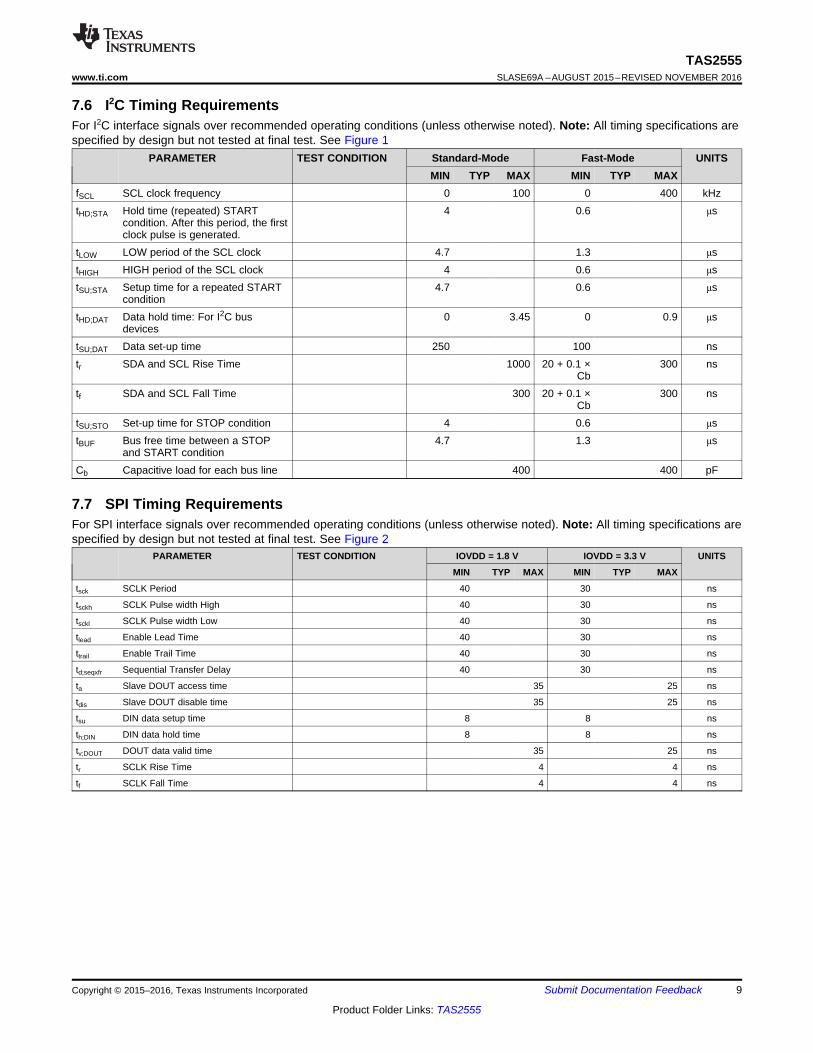
7.11 DSP Timing in Slave ModeAll specifications at 25°C, IOVDD = 1.8 V Ssee Figure 6 (1)
SYMBOL PARAMETER CONDITIONSIOVDD=1.8V IOVDD=3.3V
UNITMIN MAX MIN MAX
tH(BCLK) BCLK high period 40 30 ns
tL(BCLK) BCLK low period 40 30 ns
ts(WS) WCLK seutp 8 8 ns
th(WS) WCLK hold 8 8 ns
td(DO-BCLK) BCLK to DOUT delay (For LJF Mode only) 50% BCLK to 50% DOUT 35 25 ns
ts(DI) DIN setup 8 8 ns
th(DI) DIN hold 8 8 ns
tr Rise time 10%-90% Rise Time 8 4 ns
tf Fall time 90%-10% Fall Time 8 4 ns
Figure 1. I2C Timing
Figure 2. SPI Interface Timing Diagram

WCLK
BCLK
DOUT
DIN
td(WS) td(WS)
td(DO-BCLK)
ts(DI)th(DI)
th(WS)
WCLK
BCLK
DOUT
DIN
tL(BCLK) tH(BCLK)
ts(WS)
td(DO-WS) td(DO-BCLK)
th(DI)ts(DI)
WCLK
BCLK
DOUT
DIN
td(DO-WS)td(DO-BCLK)
tS(DI)th(DI)
td(WS)
12
TAS2555SLASE69A –AUGUST 2015–REVISED NOVEMBER 2016 www.ti.com
Product Folder Links: TAS2555
Submit Documentation Feedback Copyright © 2015–2016, Texas Instruments Incorporated
Figure 3. I2S/LJF/RJF Timing in Master Mode
Figure 4. I2S/LJF/RJF Timing in Slave Mode
Figure 5. DSP Timing in Master Mode
WCLK
BCLK
DOUT
DIN
tH(BCLK)
th(ws)
tL(BCLK)
ts(ws)th(ws)
td(DO-BCLK)
th(ws)
ts(DI)th(DI)
13
TAS2555www.ti.com SLASE69A –AUGUST 2015–REVISED NOVEMBER 2016
Product Folder Links: TAS2555
Submit Documentation FeedbackCopyright © 2015–2016, Texas Instruments Incorporated
Figure 6. DSP Timing in Slave Mode
Frequency(Hz)
TH
D+
N(%
)
20 100 1000 10000 50000500000.001
0.01
0.1
1
10
D005
VBAT=2.9VVBAT=3.6VVBAT=4.2VVBAT=5.5V
Frequency(Hz)
TH
D+
N(%
)
20 30 50 100 200 500 1000 2000 10000 50000500000.001
0.002
0.005
0.010.02
0.05
0.1
0.2
0.5
1
2
510
D006
VBAT=2.9VVBAT=3.6VVBAT=4.2VVBAT=5.5V
Pout(W)
TH
D+
N(%
)
0.001 0.010.02 0.05 0.1 0.2 0.5 1 2 3 45 7 100.001
0.002
0.005
0.010.02
0.05
0.1
0.2
0.5
1
2
510
D003
VBAT=2.9VVBAT=3.6VVBAT=4.2VVBAT=5.5V
Pout(W)
TH
D+
N(%
)
0.001 0.010.02 0.05 0.1 0.2 0.5 1 2 3 45 7 100.001
0.002
0.005
0.010.02
0.05
0.1
0.2
0.5
1
2
510
D004
VBAT=2.9VVBAT=3.6VVBAT=4.2VVBAT=5.5V
Pout(W)
TH
D+
N(%
)
0.001 0.010.02 0.05 0.1 0.2 0.5 1 2 3 45 7 100.001
0.002
0.005
0.010.02
0.05
0.1
0.2
0.5
1
2
510
D001
VBAT=2.9VVBAT=3.6VVBAT=4.2VVBAT=5.5V
Pout(W)
TH
D+
N(%
)
0.001 0.010.02 0.05 0.1 0.2 0.5 1 2 3 45 7 100.001
0.002
0.005
0.010.02
0.05
0.1
0.2
0.5
1
2
510
D002
VBAT=2.9VVBAT=3.6VVBAT=4.2VVBAT=5.5V
14
TAS2555SLASE69A –AUGUST 2015–REVISED NOVEMBER 2016 www.ti.com
Product Folder Links: TAS2555
Submit Documentation Feedback Copyright © 2015–2016, Texas Instruments Incorporated
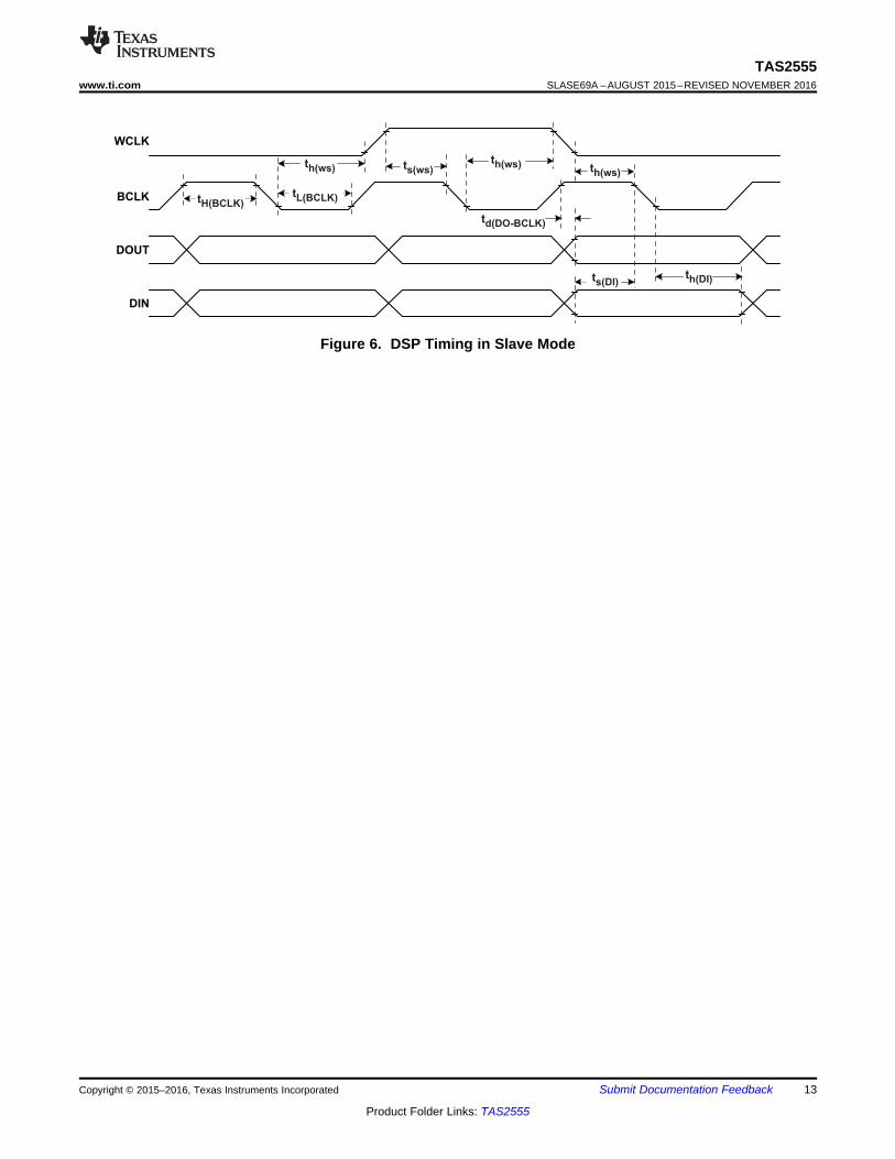
7.12 Typical CharacteristicsVBAT = 3.6 V, AVDD = IOVDD = 1.8 V, RESET = IOVDD, RL = 8 Ω + 33 µH, I2S digital input, ROM mode 1 (unless otherwisenoted).
8 Ω + 33 µH Freq = 1 kHz
Figure 7. THD+N vs Output Power
8 Ω + 33 µH Freq = 6.6 kHz
Figure 8. THD+N vs Output Power
4 Ω + 16 µH Freq = 1 kHz
Figure 9. THD+N vs Output Power
4 Ω + 16 µH Freq = 6.6 kHz
Figure 10. THD+N vs Output Power
8 Ω + 33 µH POUT = 1 W
Figure 11. THD+N vs Frequency
4 Ω + 16 µH POUT = 1 W
Figure 12. THD+N vs Frequency

Pout(W)
Effi
cien
cy(%
)
0.0005 0.01 0.05 0.2 0.5 1 2 3 45 7 100
10
20
30
40
50
60
70
80
90
100
D009
VBAT=2.9VVBAT=3.6VVBAT=4.2VVBAT=5.5V
Pout(W)
Effi
cien
cy(%
)
0.001 0.010.02 0.05 0.1 0.2 0.5 1 2 3 45 7 100
20
40
60
80
100
D010
VBAT=2.9VVBAT=3.6VVBAT=4.2VVBAT=5.5V
Frequency(Hz)
PS
RR
(dB
)
10 20 30 50 100 200 500 1000 10000 500005000075
80
85
90
95
100
105
110
115
120
D007
VBAT=3.0VVBAT=3.6VVBAT=5.4V
Frequency(Hz)
PS
RR
(dB
)
10 20 30 50 100 200 500 1000 10000 500005000075
80
85
90
95
100
105
110
115
120
D008
AVDD=1.8V
15
TAS2555www.ti.com SLASE69A –AUGUST 2015–REVISED NOVEMBER 2016
Product Folder Links: TAS2555
Submit Documentation FeedbackCopyright © 2015–2016, Texas Instruments Incorporated
Typical Characteristics (continued)VBAT = 3.6 V, AVDD = IOVDD = 1.8 V, RESET = IOVDD, RL = 8 Ω + 33 µH, I2S digital input, ROM mode 1 (unless otherwisenoted).
Figure 13. VBAT Supply Ripple Rejection vs Frequency Figure 14. AVDD Supply Ripple Rejection vs Frequency
8 Ω + 33 µH
Figure 15. Efficiency vs Output Power
4 Ω + 16 µH
Figure 16. Efficiency vs Output Power

680pF
1k��
AUX-0025
-
+
1k��
-
+
-
+
1k�0.01%
1k�0.01%
1k�0.01%
1k�0.01%
SPK_P
SPK_N
AP SYS-2772
16
TAS2555SLASE69A –AUGUST 2015–REVISED NOVEMBER 2016 www.ti.com
Product Folder Links: TAS2555
Submit Documentation Feedback Copyright © 2015–2016, Texas Instruments Incorporated
8 Parameter Measurement Information
Figure 17. TAS2555 Test Circuit
All typical characteristics for the devices are measured using the Bench EVM and an Audio Precision SYS-2722Audio Analyzer. A PSIA interface is used to allow the I2S interface to be driven directly into the SYS-2722.Speaker output terminals are connected to the Audio-Precision analyzer analog inputs through a differential-to-single ended(D2S) filter as shown below. The D2S filter contains a 1st order Passive pole at 120 kHz. The D2Sfilter ensures the TAS2555 high performance class-D amplifier sees a fully differential matched loading at itsoutputs. This prevents measurement errors due to loading effects of AUX-0025 filter on the class-D outputs.
Figure 18. Differential To Single Ended (D2S) Filter
17
TAS2555www.ti.com SLASE69A –AUGUST 2015–REVISED NOVEMBER 2016
Product Folder Links: TAS2555
Submit Documentation FeedbackCopyright © 2015–2016, Texas Instruments Incorporated
9 Detailed Description
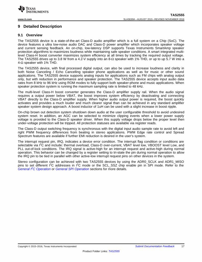
9.1 OverviewThe TAS2555 device is a state-of-the-art Class-D audio amplifier which is a full system on a Chip (SoC). Thedevice features a ultra low-noise audio DAC and Class-D power amplifier which incorporates speaker voltageand current sensing feedback. An on-chip, low-latency DSP supports Texas Instruments SmartAmp speakerprotection algorithms to maximizes loudness while maintaining safe speaker conditions. A smart integrated multi-level Class-H boost converter maximizes system efficiency at all times by tracking the required output voltage.The TAS2555 drives up to 3.8 W from a 4.2-V supply into an 8-Ω speaker with 1% THD, or up to up 5.7 W into a4-Ω speaker with 1% THD.
The TAS2555 device, with final processed digital output, can also be used to increase loudness and clarity inboth Noise Canceling / Echo Cancelling speaker phone applications as well as for music or other soundapplications. The TAS2555 device supports analog inputs for applications such as FM chips with analog outputonly, but with reduction in performance and speaker protection. The TAS2555 device accepts input audio datarates from 8 kHz to 96 kHz using ROM modes to fully support both speaker-phone and music applications. Whenspeaker protection system is running the maximum sampling rate is limited to 48 kHz.
The multi-level Class-H boost converter generates the Class-D amplifier supply rail. When the audio signalrequires a output power below VBAT, the boost improves system efficiency by deactivating and connectingVBAT directly to the Class-D amplifier supply. When higher audio output power is required, the boost quicklyactivates and provides a much louder and much clearer signal than can be achieved in any standard amplifierspeaker system design approach. A boost inductor of 1uH can be used with a slight increase in boost ripple.
On-chip brown out detection system shutdown down audio at the user configurable threshold to avoid undesiredsystem reset. In addition, an AGC can be selected to minimize clipping events when a lower power supplyvoltage is provided to the Class-D speaker driver. When this supply voltage drops below the proper level thenunder-voltage protection will be tripped. All protection statuses are available via register reads.
The Class-D output switching frequency is synchronous with the digital input audio sample rate to avoid left andright PWM frequency differences from beating in stereo applications. PWM Edge rate control and SpreadSpectrum features are available if further EMI reduction is desired in the user’s system.
The interrupt request pin, IRQ, indicates a device error condition. The interrupt flag condition or conditions areselectable via I2C and include: thermal overload, Class-D over-current, VBAT level low, VBOOST level Low, andPLL out-of-lock conditions. The IRQ signal is active-high for an interrupt request and active-high during normaloperation. This behavior can be changed by a register setting to tri-state the pin during normal operation to allowthe IRQ pin to be tied in parallel with other active-low interrupt request pins on other devices in the system.
Stereo configuration can be achieved with two TAS2555 devices by using the ADR0_SCLK and ADR1_MISOpins to set different I2C addresses in I2C mode or the SCL_SSZ chip enable pin in SPI mode. Refer to theGeneral I2C Operation or General SPI Operation sections for more details.

Boost Converter
10-Bit SAR ADC
Current Sense
Voltage Sense6�'
ADC
6�'
ADC
Programmable PLL
Missing Clock Detection and
De-Pop and Soft-Start
VOL_RAMP_Down Class-D_PWR_DOWN
Audio Clocks
MCLK
System Control
SW
Class-D Amplifier
MCLK
BCLK1
DVDD DGNDIOVDD AGND
RC CLK
VBOOST VREG
Battery
Voltage and Current Sensing
VBOOST
OSC RC CLK
TempSensor
I2C Control
I/FV
BA
T
2.2uH10 nF22 uF
SPK_P
SPK_M
MCLK
/RESET
SCL
SDA
VOL_RAMP_Down
DSPSound EnhancementVolume ControlSpeaker Excursion ProtectionSpeaker Temperature ProtectionDigital Interpolation FilteringDigital Decimation Filtering
IRQ_GPIO4MUX
OC Trip
VBAT LOW
VBOOST LOW
Over Temp
DOUT1
BCLK1
WCLK1
DIN1BaseBand and
Application Processor
ADR0
TAS2555
BCLK2
VSENSE_M
VSENSE_P
Control Registers
PVDDSW
6�'
DAC
IN_M
IN_P
IOGND
IN_P / IN_M Inputs
MUX 2
2
DOUT2
BCLK2
WCLK22Echo Canceller
Noise Canceller
AVDD
4��WR�8�Speaker
Audio Serial Interface Port #1
Programmable FormatMaster / SlaveI2S / TDM / DSP / PDMFs: 8kHz to 96kHz
Audio Serial Interface Port #2
Programmable FormatMaster / SlaveI2S / TDM / DSP / PDMFs: 8kHz to 96kHz
VBAT
PGND
Audio Serial Interface for Multi-Channel
(ASIM)
Programmable FormatMaster / SlaveI2S / TDM / DSP-Link Fs: 8kHz to 96kHz
ADR1
18
TAS2555SLASE69A –AUGUST 2015–REVISED NOVEMBER 2016 www.ti.com
Product Folder Links: TAS2555
Submit Documentation Feedback Copyright © 2015–2016, Texas Instruments Incorporated
9.2 Functional Block Diagram
9.3 Feature Description
9.3.1 General I2C OperationThe TAS2555 device operates as an I2C slave over the IOVDD voltage range. It is adjustable to one of four I2Caddresses. This allows multiple TAS2555 devices in a system to connect to the same I2C bus. The I2C pins arefail-safe. If the part has not power or is in shutdown the I2C pins will not have impact the I2C bus allowing it toremain useable.
To configure the TAS2555 for I2C operation set the SPI_SELECT pin to ground. The I2C address can then be setusing pins ADR0_SCLK and ADR1_MSIO. The pins configure the two LSB bits of the following 7-bit binaryaddress A6-A0 of 10011xx. This permits the I2C address of TAS2555 to be 0x4C(7bit) through 0x4F(7-bit). Forexample, if both ADR0_SCLK and ADR1_MSIO are connected to ground the I2C address for the TAS2555 wouldbe 0x4C(7bit). This is equivalent to 0x98 (8-bit) for writing and 0x99 (8-bit) for reading.
The I2C bus employs two signals, SDA (data) and SCL (clock), to communicate between integrated circuits in asystem. The corresponding pins on the TAS2555 for the two signals are SDA_MOSI and SCL_SSZ. The bustransfers data serially, one bit at a time. The address and data 8-bit bytes are transferred most-significant bit(MSB) first. In addition, each byte transferred on the bus is acknowledged by the receiving device with anacknowledge bit. Each transfer operation begins with the master device driving a start condition on the bus andends with the master device driving a stop condition on the bus. The bus uses transitions on the data terminal(SDA) while the clock is at logic high to indicate start and stop conditions. A high-to-low transition on SDAindicates a start, and a low-to-high transition indicates a stop. Normal data-bit transitions must occur within thelow time of the clock period. Figure 19 shows a typical sequence.

A6 A5 A4 A3 A2 A1 A0 R/W ACK A7 A6 A5 A4 A3 A2 A1 A0 ACK D7 D6 D5 D4 D3 D2 D1 D0 ACK
Start
Condition
Stop
Condition
Acknowledge Acknowledge Acknowledge
I2C Device Address and
Read/Write Bit
Register Data Byte
Register (N)8- Bit Data for 8- Bit Data for
Register (N+1)
19
TAS2555www.ti.com SLASE69A –AUGUST 2015–REVISED NOVEMBER 2016
Product Folder Links: TAS2555
Submit Documentation FeedbackCopyright © 2015–2016, Texas Instruments Incorporated
Feature Description (continued)The master generates the 7-bit slave address and the read/write (R/W) bit to open communication with anotherdevice and then waits for an acknowledge condition. The device holds SDA low during the acknowledge clockperiod to indicate acknowledgment. When this occurs, the master transmits the next byte of the sequence. Eachdevice is addressed by a unique 7-bit slave address plus R/W bit (1 byte). All compatible devices share the samesignals via a bi-directional bus using a wired-AND connection.
Use external pull-up resistors for the SDA and SCL signals to set the logic-high level for the bus. Use pull-upresistors between 660 Ω and 4.7 kΩ. Do not allow the SDA and SCL voltages to exceed the device supplyvoltage, IOVDD.
Figure 19. Typical I2C Sequence
There is no limit on the number of bytes that can be transmitted between start and stop conditions. When the lastword transfers, the master generates a stop condition to release the bus. Figure 19 shows a generic datatransfer sequence.
9.3.2 Single-Byte and Multiple-Byte TransfersThe serial control interface supports both single-byte and multiple-byte read/write operations for all registers.During multiple-byte read operations, the TAS2555 responds with data, a byte at a time, starting at the registerassigned, as long as the master device continues to respond with acknowledges.
The TAS2555 supports sequential I2C addressing. For write transactions, if a register is issued followed by datafor that register and all the remaining registers that follow, a sequential I2C write transaction has taken place. ForI2C sequential write transactions, the register issued then serves as the starting point, and the amount of datasubsequently transmitted, before a stop or start is transmitted, determines to how many registers are written.
9.3.3 Single-Byte WriteAs shown in Figure 20, a single-byte data-write transfer begins with the master device transmitting a startcondition followed by the I2C device address and the read/write bit. The read/write bit determines the direction ofthe data transfer. For a write-data transfer, the read/write bit must be set to 0. After receiving the correct I2Cdevice address and the read/write bit, the TAS2555 responds with an acknowledge bit. Next, the mastertransmits the register byte corresponding to the device internal memory address being accessed. After receivingthe register byte, the device again responds with an acknowledge bit. Finally, the master device transmits a stopcondition to complete the single-byte data-write transfer.
Figure 20. Single-Byte Write Transfer

A6 A0 ACK
Acknowledge
I2C Device Address and
Read/Write Bit
R/WA6 A0 R/W ACK A0 ACK D7 D0 ACK
Start
Condition
Stop
Condition
Acknowledge Acknowledge Acknowledge
Last Data Byte
ACK
First Data Byte
Repeat Start
ConditionNot
Acknowledge
I2C Device Address and
Read/Write Bit
Register Other Data Bytes
A7 A6 A5 D7 D0 ACK
Acknowledge
D7 D0
A6 A5 A0 R/W ACK A7 A6 A5 A4 A0 ACK A6 A5 A0 ACK
Start
Condition
Stop
Condition
Acknowledge Acknowledge Acknowledge
I2C Device Address and
Read/Write Bit
Register Data Byte
D7 D6 D1 D0 ACK
I2C Device Address and
Read/Write Bit
Not
Acknowledge
R/WA1 A1
Repeat Start
Condition
Register
20
TAS2555SLASE69A –AUGUST 2015–REVISED NOVEMBER 2016 www.ti.com
Product Folder Links: TAS2555
Submit Documentation Feedback Copyright © 2015–2016, Texas Instruments Incorporated
Feature Description (continued)9.3.4 Multiple-Byte Write and Incremental Multiple-Byte WriteA multiple-byte data write transfer is identical to a single-byte data write transfer except that multiple data bytesare transmitted by the master device to the TAS2555 as shown in Figure 21. After receiving each data byte, thedevice responds with an acknowledge bit.
Figure 21. Multiple-Byte Write Transfer
9.3.5 Single-Byte ReadAs shown in Figure 22, a single-byte data-read transfer begins with the master device transmitting a startcondition followed by the I2C device address and the read/write bit. For the data-read transfer, both a writefollowed by a read are actually done. Initially, a write is done to transfer the address byte of the internal memoryaddress to be read. As a result, the read/write bit is set to a 0.
After receiving the TAS2555 address and the read/write bit, the device responds with an acknowledge bit. Themaster then sends the internal memory address byte, after which the device issues an acknowledge bit. Themaster device transmits another start condition followed by the TAS2555 address and the read/write bit again.This time, the read/write bit is set to 1, indicating a read transfer. Next, the TAS2555 transmits the data byte fromthe memory address being read. After receiving the data byte, the master device transmits a not-acknowledgefollowed by a stop condition to complete the single-byte data read transfer.
Figure 22. Single-Byte Read Transfer
9.3.6 Multiple-Byte ReadA multiple-byte data-read transfer is identical to a single-byte data-read transfer except that multiple data bytesare transmitted by the TAS2555 to the master device as shown in Figure 23. With the exception of the last databyte, the master device responds with an acknowledge bit after receiving each data byte.
Figure 23. Multiple-Byte Read Transfer

VBAT
Ou
tpu
t V
olt
ag
e
VLIMPeak
Inflection PointBrownout
Shutdown Battery Guard Speaker Guard
VLIMTracking
21
TAS2555www.ti.com SLASE69A –AUGUST 2015–REVISED NOVEMBER 2016
Product Folder Links: TAS2555
Submit Documentation FeedbackCopyright © 2015–2016, Texas Instruments Incorporated
Feature Description (continued)9.3.7 General SPI OperationThe TAS2555 operates as an SPI slave over the IOVDD voltage range.
9.3.8 Class-D Edge Rate ControlThe edge rate of the Class-D output is controllable via I2C register B0_P0_R6[2:0]. This allows users the abilityto adjust the switching edge rate of the Class-D amplifier, trading off some efficiency for lower EMI. Table 1 liststhe typical edge rates. The default edge rate of 14ns passes EMI testing. The default value is recommended butmay be changed if requried.
Table 1. Class-D Edge Rate ControlDAC_EDGE BYTE:
DAC_EDGE[2:0]tR AND tF(TYPICAL)
010 29 ns011 25 ns100 14 ns (default)101 13 ns110 12 ns111 11 ns
9.3.9 Battery Tracking AGCThe TAS2555 device monitors battery voltage and the audio signal to automatically decrease gain when thebattery voltage is low and audio output power is high. This provides louder audio while preventing early shutdownat end-of-charge battery voltage levels. The battery tracking AGC starts to attenuate the signal once the voltageat the Class-D output exceeds VLIM for a given battery voltage (VBAT). If the Class-D output voltage is below theVLIM value, no attenuation occurs. If the Class-D output exceeds the VLIM value the AGC starts to attack thesignal and reduce the gain until the output is reduced to VLIM. Once the signal returns below VLIM plus somehysteresis the gain reduction decays. The VLIM is constant above the user configurable inflection point. Below theinflection point the VLIM is reduced by a user configurable slope in relation to the battery voltage. The attack time,decay time, inflection point and VLIM/VBAT slope below the inflection point are user configurable. The parametersfor the Battery Tracking AGC are part of the DSP core and can be set using thePurePath™ Console 3 SoftwareTAS2555 Application software for the TAS2555 device part under the Device Control Tab. Below a VBAT level of2.9 V, the boost will turn on to ensure correct operation but results in increased current consumption. The deviceis functional until the set brownout level is reached and the device shuts down. The minimum brownout voltage is2.7 V.
Figure 24. VLIM versus Supply Voltage (VBAT)
9.3.10 Configurable Boost Current Limit (ILIM)The TAS2555 device has a configurable boost current limit (ILIM). The default current limit is 3 A but this limitmay be set lower based on selection of passive components connected to the boost. The TAS2555 devicesupports 4 different boost limits.
22
TAS2555SLASE69A –AUGUST 2015–REVISED NOVEMBER 2016 www.ti.com
Product Folder Links: TAS2555
Submit Documentation Feedback Copyright © 2015–2016, Texas Instruments Incorporated
Table 2. Current Limit SettingsCURRENT LIMIT REGISTER
B0_P0_R43_D[1:0]BOOST CURRENT LIMIT (ILIM)
(A)00 1.501 2.010 2.511 3.0 (default)
9.3.10.1 Fault ProtectionThe TAS2555 device has several protection blocks to prevent damage. Those blocks including how to resumefrom a fault are presented in this section.
9.3.10.1.1 OverCurrent
The TAS2555 device has an integrated overcurrent protection that is enabled once the Class-D is powered up. Afault on the Class-D output causing a large current in the range of 3 A to 5 A triggers the overcurrent fault. Oncethe fault is detected the TAS2555 device disables the audio channel and power down the Class-D amplifier.When an over-current event occurs, a status flag at B0_P0_R104[7] is set. This register is sticky and the bitremains high for as long as it is not read, or the device is not reset. The overcurrent event can also be used togenerate an interrupt if required. Refer to "IRQ and flags" section for more details. To re-enable the audiochannel after a fault the Class-D the device must be hardware or software reset and the TAS2555 configurationmust be re-loaded.
9.3.10.1.2 Analog Undervoltage
The TAS2555 device has an integrated undervoltage protection on the analog power supply lines AVDD andVBAT. The undervoltage limit fault is triggered when AVDD is less than 1.5 V or when VBAT is less than 2.4 V.Once the fault is detected the TAS2555 device will disable the audio channel and power down the Class-Damplifier. When an under-voltage event occurs, a status flag at B0_P0_R104[6] is set. This register is sticky andthe bit will remain high for as long as it is not read, or the device is not reset. The undervoltage event can also beused to generate an interrupt if required. Refer to IRQs and Flags section for more details. To re-enable theaudio channel after a fault the Class-D must be re-enabled by setting B0_P0_R5[7]=1. All other configurationsare preserved and the audio channel will power up with the last configured settings.
9.3.10.1.3 Overtemperature
The TAS2555 device has an integrated overtemperature protection that is enabled once the Class-D is poweredup. If the device internal junction temperature exceeds the safe operating region it will trigger theovertemperature fault. Once the fault is detected the TAS2555 device disables the audio channel and powerdown the Class-D amplifier. The device waits until the user reads the overtemperature flag in B0_P0_R104[4] tore-enable the Class-D amplifier if the junction temperature returns into a safe operating region. When an over-temperature event occurs, a status flag at B0_P0_R104[4] is set. This register is sticky and the bit will remainhigh for as long as it is not read, or the device is not reset. The overtemperature event can also be used togenerate an interrupt if required. Refer to IRQs and Flags section for more details. The overtemperatureautomatic re-enable can be disabled by setting B0_P2_R9[2]=1. If the automatic re-enable is disabled, to re-enable the audio channel after the overtemperature fault the Class-D must be re-enabled by settingB0_P0_R5[7]=1. All other configurations are preserved and the audio channel will power up with the lastconfigured settings.
9.3.10.1.4 Clocking Faults
The TAS2555 device has two clock error detection blocks. The first is on the Audio Serial Interfaces (ASI). If aclock error is detected on the ASI interfaces audio artifacts can occur at the Class-D output. When enabled theASI clock error detection can mute the device and shutdown the Class-D and DSP core. The clock errordetection block is enabled by setting register bit B0_P0_R44[1]=1. The ASI1 or ASI2 clocks can be routed to theblock for detection using register B0_P0_R44[4]. Additionally, the clock error can be routed to an interrupt pinand the sticky bit at register B0_P0_R104[5] indicates the clock error occurred. The second clock error detectionblock can monitor the DAC, ADC, and PLL clocks. When a clock error is detected the output is soft-muted andthe Class-D powered down. This clock error detection is enabled using register bit B0_P0_R44[0], can be routedto interrupt pin and is indicated in the sticky bit B0_P0_R104[2].

23
TAS2555www.ti.com SLASE69A –AUGUST 2015–REVISED NOVEMBER 2016
Product Folder Links: TAS2555
Submit Documentation FeedbackCopyright © 2015–2016, Texas Instruments Incorporated
When a clocking error occurs the following sequence should be performed to restart the device.
• Clear the clock error interrupts by reading the sticky flags at registers B0_P0_R104 and B0_P0_R108• Disable the clock error detection blocks by writing B0_P0_R44[7:0]=0x00 as the internal dividers will be
stopped on error detection.• Shutdown by writing B0_P0_R4=0x00 and B0_P0_R5=0x00• Re-power appropriate devices in the same registers• Re-enable the clock error detection blocks in register B0_P0_R44
9.3.10.2 BrownoutThe TAS2555 device has an integrated brownout system to shutdown the device when the battery voltage dropsto an insufficient level. This user configurable level can be set under Device Control in the PurePath™ Console 3Software TAS2555 Application. When brownout event occurs a status flag B0_P0_R104[3] is set. This register issticky and the bit remains high for as long as it is not read, or the device is not reset. The brownout event canalso be used to generate an interrupt if required. Refer to IRQs and Flags section for more details. Once thebattery voltage drops below the defined threshold the following actions occur.• The audio playback is muted in a graceful soft-stepping manner• DSP, clock dividers, and analog blocks are powered down. B0_P0_R4[7:3]=00000 and B0_P0_R5[7:0]=0x00• Sticky bit B0_P0_R104[3] is set
Once the host is aware of the brownout it should write B0_P0_R4[0] =0 to put the TAS2555 device in softwareshutdown and enter low power mode. Once the battery supply is stable above the defined brownout thresholdthe host can re-enable the device using the Power Control Registers B0_P0_R4 and B0_P0_R5.
9.3.10.3 Spread Spectrum vs SynchronizedThe Class-D switching frequency can be selected to work in two different modes of operations. This configurationmust be done before powering up the audio channel. The first is a synchronized mode where the Class-Dfrequency is synchronized frequency to audio input sample rate. This is the default mode of operation and shouldbe used in stereo applications to avoid inter-modulation beating of the Class-D frequency from multiple chips.The Class-D switching frequency in this mode can be configured as 384 kHz for 352.8 kHz. The 384 kHzfrequency is the default mode of operation, and can be used for input signals running on clock rates of 48 kHz orits sub-multiples. For input signals running on clock rate of 44.1 kHz and its sub-multiples, the switchingfrequency can be selected as 352.8 kHz by setting B0_P2_R6[4]=1.
The second mode is spread-spectrum mode used to reduce wideband spectral content, improving EMI emissionsradiated by the speaker. In this mode, the Class-D switching frequency varies +-5% about a 384 kHz centerfrequency. This mode can be configured by setting B0_P0_R40[0]=1 and B100_P0_R40[7]=0. Both theseregisters should be written before powering up the audio channel.
9.3.10.4 IRQs and FlagsInternal device flags such as overcurrent, under-voltage, etc can be routed as interrupts. The device has 4interrupts that can be routed to any of the 10 GPIO pins. If more than one flag is assigned to the same interruptthe interrupt output is the logical OR-ing of all flags. If multiple flags are assigned to the same interrupt the hostshould then query the flags sticky register to determine which event triggered the interrupt. The 10 GPIO pinscan be configured for any interrupt and can be configured using B0_P1_R61 thru B0_P1_R70.
Table 3. Interrupt RegistersFlag Name Flag Description Sticky Register Bit Register to Route Flag to Interrupt
Flag 1 Over Current B0_P0_R104[7] B0_P1_R108[6:4]Flag 2 Under Voltage B0_P0_R104[6] B0_P1_R108[2:0]Flag 3 Clock Error Detection 1 B0_P0_R104[5] B0_P1_R109[6:4]Flag 4 Over Temperature B0_P0_R104[4] B0_P1_R109[2:0]Flag 5 Brownout B0_P0_R104[3] B0_P1_R110[6:4]Flag 6 Clock Error Detection 2 B0_P0_R104[2] B0_P1_R110[2:0]Flag 7 SAR Complete B0_P0_R104[1] B0_P1_R111[6:4]

24
TAS2555SLASE69A –AUGUST 2015–REVISED NOVEMBER 2016 www.ti.com
Product Folder Links: TAS2555
Submit Documentation Feedback Copyright © 2015–2016, Texas Instruments Incorporated
For example, to route the Brownout and Under Voltage flags to GPIO5 (Pin IRQ_GPIO5) the following registersettings would be used. The flag Brownout would be routed to Interrupt 1 by setting B0_P1_R110[6:4]=001 andflag Under Voltage would be also routed to interrupt 1 by setting B0_P1_R108[2:0]=001. The pin IRQ_GPIO5would be set to use interrupt 1 by setting B0_P1_R64[4:0]=0x07
9.3.10.5 Software ResetThe TAS2555 device internal logic must be initialized to a known condition for proper device function by doing asoftware reset. Performing software reset after a hardware reset is mandatory for reliable device boot up. Toperform software reset write ‘1’ to B0_P0_R1_D0. After reset, all registers are initialized with default values aslisted in the Register Map. After software reset is performed, no register read/write should be performed within100us.
9.3.10.6 PurePath™ Console 3 Software TAS2555 ApplicationThe TAS2555 device contains an integrated DSP processing engine for advance speaker protection. Theadvanced features and a significant portion of the device configuration is performed using this tool. The basesoftware is called Pure Path Console 3 (PPC3). Once the software is downloaded and installed from the TIwebsite, the TAS2555 application can be download from with-in the software. The datasheet refers to optionsthat can be configured using the PPC3 software tool.
9.4 Device Functional Modes
9.4.1 Audio Digital I/O InterfaceAudio data is transferred between the host processor and the TAS2555 device via the digital audio data serialinterface, or audio bus. The audio bus on this device is flexible, including left or right-justified data options,support for I2S or PCM protocols, programmable data length options, a TDM mode for multichannel operation,very flexible master/slave configurability for each bus clock line, and the ability to communicate with multipledevices within a system directly.
The audio bus of the TAS2555 device can be configured for left or right-justified, I2S, DSP, or TDM modes ofoperation, where communication with standard telephony PCM interfaces is supported within the TDM mode.These modes are all MSB-first, with data width programmable as 16, 20, 24, or 32 bits by configuring RegistersB0_P1_R1_D[4:3] and B0_P1_R2_D[4:3] for ASI1 and Registers B0_P1_R21_D[4:3] and B0_P1_R22_d[4:3] . Inaddition, the word clock and bit clock can be independently configured in either Master or Slave mode, forflexible connectivity to a wide variety of processors. The word clock is used to define the beginning of a frame,and may be programmed as either a pulse or a square-wave signal. The frequency of this clock corresponds tothe maximum of the selected ADC and DAC sampling frequencies.
The bit clock is used to clock in and clock out the digital audio data across the serial bus. This signal can beprogrammed to generate variable clock pulses by controlling the bit-clock multiply-divide factor in Registers 0x08through 0x10. The number of bit-clock pulses in a frame may require adjustment to accommodate various word-lengths as well as to support the case when multiple TAS2555 devices may share the same audio bus.
The TAS2555 device also includes a feature to offset the position of start of data transfer with respect to theword-clock. This offset is in number of bit-clocks and is programmed in Register 0x06.
To place the DOUT line into a Hi-Z (3-state) condition during all bit clocks when valid data is not being sent, setRegister B0_P1_R1_D[0] = 1 for ASI1 and Register B0_P1_R21[0] = 1. By combining this capability with theability to program what bit clock in a frame the audio data begins, time-division multiplexing (TDM) can beaccomplished. This enables the use of multiple devices on a single audio serial data bus. When the audio serialdata bus is powered down while configured in master mode, the terminals associated with the interface are putinto a Hi-Z output state.
9.4.1.1 Right-Justified Mode (RJF)Audio Serial Interface 1 can be put into Right Justified Mode by programming B0_P1_R1_D[7:5] = 010 andB0_P1_R2_D[7:5] = 010 . Audio Serial Interface 2 can be put into Right Justified Mode byprogrammingB0_P1_R21_D[7:5] = 010 and B0_P1_R22_D[7:5] = 010. In right-justified mode, the LSB of the leftchannel is valid on the rising edge of the bit clock preceding the falling edge of the word clock. Similarly, the LSBof the right channel is valid on the rising edge of the bit clock preceding the rising edge of the word clock.

BCLK
WCLK
DIN/
DOUTn-1 n-2 1 00 n-1 n-2 1 0
LSBMSB
Left Channel Right Channel
n-3 2 2n-3
LSBMSB
1/fs
25
TAS2555www.ti.com SLASE69A –AUGUST 2015–REVISED NOVEMBER 2016
Product Folder Links: TAS2555
Submit Documentation FeedbackCopyright © 2015–2016, Texas Instruments Incorporated
Device Functional Modes (continued)
Figure 25. Timing Diagram for Right-Justified Mode
For right-justified mode, the number of bit-clocks per frame should be greater than twice the programmed word-length of the data.

LD(n) LD(n+1)
WORDCLOCK
BITCLOCK
DATA 3N-1
N-2
N-3
2 1 03N-1
N-2
N-3
2 1 03N-1
N-2
N-3
RD(n)
LEFT CHANNEL RIGHT CHANNEL
LD(n) = n'th sample of left channel data RD(n) = n'th sample of right channel data
LD(n) LD(n+1)
WORDCLOCK
BITCLOCK
DATA -1
-2
-3
2 1 03 -1
-2
-3
2 1 03 -1
-2
N N N N N N N N N-3
RD(n)
LEFT CHANNEL RIGHT CHANNEL
LD(n) = n'th sample of left channel data RD(n) = n'th sample of right channel data
LD(n) LD(n+1)
WORDCLOCK
BITCLOCK
DATA -1
-2
-3
2 1 03 -1
-2
-3
2 1 03 -1
-2
N N N N N N N N N-3
RD(n)
LEFT CHANNEL RIGHT CHANNEL
LD(n) = n'th sample of left channel data RD(n) = n'th sample of right channel data
26
TAS2555SLASE69A –AUGUST 2015–REVISED NOVEMBER 2016 www.ti.com
Product Folder Links: TAS2555
Submit Documentation Feedback Copyright © 2015–2016, Texas Instruments Incorporated
Device Functional Modes (continued)9.4.1.2 Left-Justified Mode (LJF)Audio Serial Interface 1 can be put into left-justified mode by programming B0_P1_R1_D[7:5] = 011 andB0_P1_R2_D[7:5] = 011 . Audio Serial Interface 2 can be put into left-justified mode by programmingB0_P1_R21_D[7:5] = 011 and B0_P1_R22_D[7:5] = 011. In left-justified mode, the MSB of the right channel isvalid on the rising edge of the bit clock following the falling edge of the word clock. Similarly the MSB of the leftchannel is valid on the rising edge of the bit clock following the rising edge of the word clock.
Figure 26. Timing Diagram for Left-Justified Mode
Figure 27. Timing Diagram for Light-Left Mode with Offset = 1
Figure 28. Timing Diagram for Left-Justified Mode with Offset = 0 and Inverted Bit Clock
For left-justified mode, the number of bit-clocks per frame should be greater than twice the programmed word-length of the data. Also, the programmed offset value should be less than the number of bit-clocks per frame byat least the programmed word-length of the data.
LD(n) LD(n+1)
WORDCLOCK
BITCLOCK
DATA -1
-2
-3
2 1 03 -1
-2
-3
2 1 03 -1
-2
N N N N N N N N N-3
3
RD(n)
LEFT CHANNEL RIGHT CHANNEL
LD(n) = n'th sample of left channel data RD(n) = n'th sample of right channel data
LD(n) LD (n+1)
WORDCLOCK
BITCLOCK
DATA -1
4 3 25 1 0 -1
4 3 25 1 0N N N
-1
5
RD(n)
LEFT CHANNEL RIGHT CHANNEL
LD(n) = n'th sample of left channel data RD(n) = n'th sample of right channel data
LD(n) LD(n+1)
WORDCLOCK
BITCLOCK
DATA -1
-2
-3
2 1 03 -1
-2
-3
2 1 03 -1
-2
N N N N N N N N N-3
3
RD(n)
LEFT CHANNEL RIGHT CHANNEL
LD(n) = n'th sample of left channel data RD(n) = n'th sample of right channel data
27
TAS2555www.ti.com SLASE69A –AUGUST 2015–REVISED NOVEMBER 2016
Product Folder Links: TAS2555
Submit Documentation FeedbackCopyright © 2015–2016, Texas Instruments Incorporated
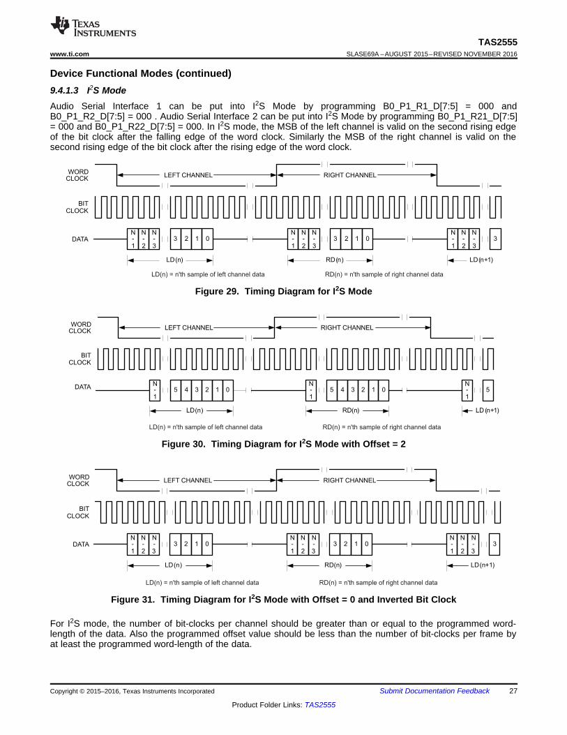
Device Functional Modes (continued)9.4.1.3 I2S ModeAudio Serial Interface 1 can be put into I2S Mode by programming B0_P1_R1_D[7:5] = 000 andB0_P1_R2_D[7:5] = 000 . Audio Serial Interface 2 can be put into I2S Mode by programming B0_P1_R21_D[7:5]= 000 and B0_P1_R22_D[7:5] = 000. In I2S mode, the MSB of the left channel is valid on the second rising edgeof the bit clock after the falling edge of the word clock. Similarly the MSB of the right channel is valid on thesecond rising edge of the bit clock after the rising edge of the word clock.
Figure 29. Timing Diagram for I2S Mode
Figure 30. Timing Diagram for I2S Mode with Offset = 2
Figure 31. Timing Diagram for I2S Mode with Offset = 0 and Inverted Bit Clock
For I2S mode, the number of bit-clocks per channel should be greater than or equal to the programmed word-length of the data. Also the programmed offset value should be less than the number of bit-clocks per frame byat least the programmed word-length of the data.

LD(n) LD(n+1)
BITCLOCK
DATAN-1
N-2
N-3
2 1 03N-1
N-2
N-3
03 2 1N-1
N-2
N-3
3
RD(n)
WORDCLOCK
LEFT CHANNEL RIGHT CHANNEL
LD(n) LD(n+1)
BITCLOCK
DATA -1
-2
-3
2 1 03 -1
-2
-3
03 2 1 -1
-2
N N N N N N N N N-3
RD(n)
WORDCLOCK
LEFT CHANNEL RIGHT CHANNEL
LD(n) = n'th sample of left channel data RD(n) = n'th sample of right channel data
LD(n) LD(n+1)
BITCLOCK
DATA -1
-2
-3
2 1 03 -1
-2
-3
03 2 1 -1
-2
N N N N N N N N N-3
3
RD(n)
WORDCLOCK
LEFT CHANNEL RIGHT CHANNEL
LD(n) = n'th sample of left channel data RD(n) = n'th sample of right channel data
28
TAS2555SLASE69A –AUGUST 2015–REVISED NOVEMBER 2016 www.ti.com
Product Folder Links: TAS2555
Submit Documentation Feedback Copyright © 2015–2016, Texas Instruments Incorporated
Device Functional Modes (continued)9.4.1.4 DSP ModeAudio Serial Interface 1 can be put into DSP Mode by programming B0_P1_R1_D[7:5] = 001 andB0_P1_R2_D[7:5] = 001 . Audio Serial Interface 2 can be put into DSP Mode by programmingB0_P1_R21_D[7:5] = 001 and B0_P1_R22_D[7:5] = 001. In DSP mode, the rising edge of the word clock startsthe data transfer with the left channel data first and immediately followed by the right channel data. Each data bitis valid on the falling edge of the bit clock.
Figure 32. Timing Diagram for DSP Mode
Figure 33. Timing Diagram for DSP Mode with Offset=1
Figure 34. Timing Diagram for DSP Mode with Offset=0 and Inverted Bit Clock
For DSP mode, the number of bit-clocks per frame should be greater than twice the programmed word-length ofthe data. Also the programmed offset value should be less than the number of bit-clocks per frame by at leastthe programmed word-length of the data.

6 Biquad EQ
0/1
Volum
e Battery Guard
0/1 Brownout
Vbatt
AS
I Port
Class-H
Boost On/Off
Boost Level
DACVbatt
LD(n) LD (n+1)
WORDCLOCK
BITCLOCK
DATA -1
4 3 25 1 0 -1
4 3 25 1 0N N N
-1
5
RD(n)
LEFT CHANNEL RIGHT CHANNEL
LD(n) = n'th sample of left channel data RD(n) = n'th sample of right channel data
29
TAS2555www.ti.com SLASE69A –AUGUST 2015–REVISED NOVEMBER 2016
Product Folder Links: TAS2555
Submit Documentation FeedbackCopyright © 2015–2016, Texas Instruments Incorporated
Device Functional Modes (continued)9.4.2 TDM ModeTime-division multiplexing (TDM) allows two or more devices to share a common DIN connection and a commonDOUT connection. Using TDM mode, all devices transmit their DOUT data in user-specified sub-frames withinone WCLK period. When one device transmits its DOUT information, the other devices place their DOUTterminals in a high impedance tri-state mode.
TDM mode is useable with I2S, LJF, RJF, and DSP interface modes. Refer to the respective sections for adescription of how to set the TAS2555 device into those modes.
Use Register B0_P1_R3 for ASI1 and B0_P1_R23 for ASI2 to set the clock cycle offset from WCLK to the MSB.Each data bit is valid on the falling edge of the bit clock. Set Register B0_P1_R1_D[0] = 1 for ASI1 andB0_P1_R21_D[0] = 1 to force DOUT into tri-state when it is not transmitting data. This allows DOUT terminalsfrom multiple TAS2555 devices to share a common wire to the host.
Figure 35. Timing Diagram for I2S in TDM Mode with Offset=2
For TDM mode, the number of bit-clocks per frame should be less than the programmed word-length of the data.Also the programmed offset value should be less than the number of bit-clocks per frame by at least theprogrammed word-length of the data.
9.4.3 Device Digital Processing ModesThe TAS2555 DSP can be initialized into one of three modes.
9.4.3.1 ROM Mode 1ROM mode 1 provides the quickest initialization from the TAS2555 initial power up and is the lowest powermode. This mode can be used to play a known power up audio sequence before the rest of the audio systemsoftware is loaded. The mode provides fault protection, brownout protection volume control, and class-Hcontroller. With minimal additional configuration the EQ and Battery Guard can be enabled. The speakerprotection algorithm is not running in this mode and the I/V sense ADC are powered down to minimize powerconsumption. The PLL can be disabled for even lower power consumption if the MCLK supplied is at least12.288MHz for any fs which is multiple or sub-multiple of 48kHz, or 11.2896MHz for fs of 44.1kHz. This mode isset by writing B)_P0_R34[7:0]=0x21 before powering up the DSP B0_P0_R4[7]. This mode should be used tocharacterize the electrical performance on the TAS2555 device without any influence from the protectionalgorithm present in other modes.
Figure 36. ROM Mode 1 Processing Block Diagram

6 Biquad EQ
0/1
Volum
e Battery Guard
0/1 Brownout
Vbatt
AS
I In Class-H
Boost On/Off
Boost Level
DACVbatt
ICN/IVsense Control
ADC I
ADC V
AS
I Out L/
R M
ix
30
TAS2555SLASE69A –AUGUST 2015–REVISED NOVEMBER 2016 www.ti.com
Product Folder Links: TAS2555
Submit Documentation Feedback Copyright © 2015–2016, Texas Instruments Incorporated
Device Functional Modes (continued)9.4.3.2 ROM Mode 2ROM mode 2 is similar to ROM mode 1 except the I/V sense ADCs are powered up and the data is routed backon the L/R return channels of the ASI port. This mode can be used to return the I/V data to the host and performalternate computations on the speaker I/V measurements. This mode is set by writing B0_P0_R34[7:0]=0x22before powering up the DSP B0_P0_R4[7].
Figure 37. ROM Mode 1 Processing Block Diagram
9.4.3.3 SmartAmp ModeSmartAmp Mode is used to run the TI SmartAmp algorithm on the built in DSP. This mode involves loadinglarger output files generated from the PurePath™ Console 3 Software TAS2555 Application. The generated filescontain the speaker models, equalization, and additional configuration parameters in a format to load over theI2C or SPI interface. TI's SmartAmp provides Thermal and Excursion protection using initial speaker models andthe current and voltage feedback to determine exact coil temperature and update the initial model due tovariations in speaker and ambient conditions. More information about this mode can be found in the PurePath™Console 3 Software TAS2555 Application.
9.4.4 Low Power Sleep ModeThe device has a low power sleep mode option to reduce the power consumption on analog supplies (AVDD andVBAT). There are two lower power modes and the choice depends on AVDD supply. First, if the AVDD supplydoes not drop below the minimum specified voltage, the lowest power mode can be activated by performing asoftware reset B0_P0_R1[0]=1, waiting 100us and then writing shutdown POR blocks B0_P0_R121[7]=1. To exitthe low power sleep mode write B0_P0_R121[7]=0 to power up the Avdd and Vbat POR. The part ideally can beplaced in low power mode by only shutting down the POR blocks. However, due to non-default configurations TIrecommends the software reset.
If the AVDD POR must remain enabled an alternate low power mode should be used. To enable the second lowpower mode write B0_P0_R4[7:0]=0 and B0_P0_R5[7:0]=0.
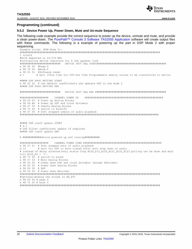
9.5 Programming
9.5.1 Code Loading and CRC checkThe TI SmartAmp software is loaded into program ram(PRAM) through writes to mapped memory registers. Theencrypted binary software is downloaded and decoded on chip. Therefore read-back of the PRAM is disabled.However a 8 bit CRC checksum is provided to the customer to verify the code was correctly written to PRAMerror-free. Once the software download is complete the calculated 8-bit CRC checksum can be read fromB0_P0_R32. If this value matches the checksum supplied with the program the load to PRAM was successful. Ifnew PRAM code is loaded the TAS2555 device should first be software or hardware reset to reset the CRCchecksum register to obtain a proper checksum from the new code to be loaded.
31
TAS2555www.ti.com SLASE69A –AUGUST 2015–REVISED NOVEMBER 2016
Product Folder Links: TAS2555
Submit Documentation FeedbackCopyright © 2015–2016, Texas Instruments Incorporated
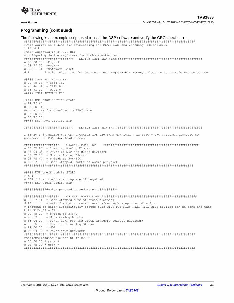
Programming (continued)The following is an example script used to load the DSP software and verify the CRC checksum.
##############################################################################################This script is a demo for downloading the PRAM code and checking CRC checksumi i2cstd#mclk expected is 24.576 MHz#configuring device registers for 8 ohm speaker load########################### DEVICE INIT SEQ START##############################################w 98 00 00 #Page-0w 98 7f 00 #Book-0w 98 01 01 #Software resetd 1 # wait 100us time for OTP-One Time Programmable memory values to be transferred to device
##### INIT SECTION STARTw 98 7f 64 # book 100w 98 46 01 # IRAM bootw 98 7f 00 # book 0##### INIT SECTION END
##### DSP PROG SETTING STARTw 98 7f 64w 98 00 01#add writes for download to PRAM herew 98 00 00w 98 7f 00##### DSP PROG SETTING END
########################### DEVICE INIT SEQ END ###############################################
r 98 20 1 # reading the CRC checksum for the PRAM download , if read = CRC checksum provided tocustomer => PRAM download success
################### CHANNEL POWER UP ####################################################w 98 05 A3 # Power up Analog Blocksw 98 04 B8 # Power up DSP and clock dividersw 98 07 00 # Unmute Analog Blocksw 98 7f 64 # switch to book100w 98 07 00 # Soft stepped unmute of audio playback############################################################################################
##### DSP coeff update START# d 1# DSP filter coefficient update if required##### DSP coeff update END
############device powered up and running##########
################### CHANNEL POWER DOWN ####################################################w 98 07 01 # Soft stepped mute of audio playbackd 10 # wait for DSP to mute classD after soft step down of audio# instead of delay alternatively status flag B120_P15_R120_R121_R122_R123 polling can be done and waittill R122_D0 = '1'.w 98 7f 00 # switch to book0w 98 07 03 # Mute Analog Blocksw 98 04 20 # Power down DSP and clock dividers (except Ndivider)w 98 05 00 # Power down Analog Blocksw 98 00 00 # NOPw 98 04 00 # Power down Ndivider##############################################################################################optional(ending the script in B0_P0)w 98 00 00 # page 0w 98 7f 00 # book 0#############################################################################################
32
TAS2555SLASE69A –AUGUST 2015–REVISED NOVEMBER 2016 www.ti.com
Product Folder Links: TAS2555
Submit Documentation Feedback Copyright © 2015–2016, Texas Instruments Incorporated
Programming (continued)9.5.2 Device Power Up, Power Down, Mute and Un-mute SequenceThe following code example provide the correct sequence to power up the device, unmute and mute, and providea clean power-down. The PurePath™ Console 3 Software TAS2555 Application software will create output fileswith these commands. The following is a example of powering up the part in DSP Mode 2 with propersequencing.
Example script (ROM Mode 2):#############################################################################################i i2cstd#mclk expected is 24.576 MHz#configuring device registers for 8 ohm speaker load########################### DEVICE INIT SEQ START##############################################w 98 00 00 #Page-0w 98 7f 00 #Book-0w 98 01 01 #Software resetd 1 # wait 100us time for OTP-One Time Programmable memory values to be transferred to device
##### DSP PROG SETTING STARTw 98 22 22 # use default coefficients and operate DSP in rom mode 2##### DSP PROG SETTING END
########################### DEVICE INIT SEQ END ###############################################
################### CHANNEL POWER UP ####################################################w 98 05 A3 # Power up Analog Blocksw 98 04 B8 # Power up DSP and clock dividersw 98 07 00 # Unmute Analog Blocksw 98 7f 64 # switch to book100w 98 07 00 # Soft stepped unmute of audio playback############################################################################################
##### DSP coeff update START# d 1# DSP filter coefficient update if required##### DSP coeff update END
b ############device powered up and running##########
################### CHANNEL POWER DOWN ####################################################w 98 07 01 # Soft stepped mute of audio playbackd 10 # wait for DSP to mute classD after soft step down of audio# instead of delay alternatively status flag B120_P15_R120_R121_R122_R123 polling can be done and waittill R122_D0 = '1'.w 98 7f 00 # switch to book0w 98 07 03 # Mute Analog Blocksw 98 04 20 # Power down DSP and clock dividers (except Ndivider)w 98 05 00 # Power down Analog Blocksw 98 00 00 # NOPw 98 04 00 # Power down Ndivider##############################################################################################optional(ending the script in B0_P0)w 98 00 00 # page 0w 98 7f 00 # book 0#############################################################################################

VBAT
SPK_M
SPK_PADR0/1
VBOOST
SW
L2 (opt.)
I2C
I2S
IOVDD10 nF
C222 PF
VREG
VSENSE_M
VSENSE_P
L12.2 PH
2.9 V À 5.5 V
AGND
L3 (opt.)
ToSpeaker
+
-
DVDD
/RESET
SPI_SELECT
5
2
PGND
2
3
0.1 PF
C110 PF
C31 nF(opt.)
C41 nF(opt.)
0.1 PF
1.65 V À 1.95 V
1.62 V À3.6 V
I2C Address Select
Enable
I2C Interface
I2S Interface
0.1 PF
VSENSE
2
2
AVDD
0.1 PF
1.65 VÀ 1.95 V
IOGND
1 PF
1 PF1 PF
0.1 PF
33
TAS2555www.ti.com SLASE69A –AUGUST 2015–REVISED NOVEMBER 2016
Product Folder Links: TAS2555
Submit Documentation FeedbackCopyright © 2015–2016, Texas Instruments Incorporated
10 Applications and Implementation
NOTEInformation in the following applications sections is not part of the TI componentspecification, and TI does not warrant its accuracy or completeness. TI’s customers areresponsible for determining suitability of components for their purposes. Customers shouldvalidate and test their design implementation to confirm system functionality.
10.1 Application InformationThe TAS2555 device is a digital or analog input high efficiency Class-D audio power amplifier with advancedbattery current management and an integrated Class-H boost converter. In auto passthrough mode, the Class-Hboost converter generates the Class-D amplifier supply rail. During low Class-D output power, the boostimproves efficiency by deactivating and connecting VBAT directly to the Class-D amplifier supply. When highpower audio is required, the boost quickly activates to provide louder audio than a stand-alone amplifierconnected directly to the battery. To enable load monitoring, the TAS2555 device constantly measures thecurrent and voltage across the load and provides a digital stream of this information back to a processor.
10.2 Typical Applications
Figure 38. Typical Application - Digital Audio Input
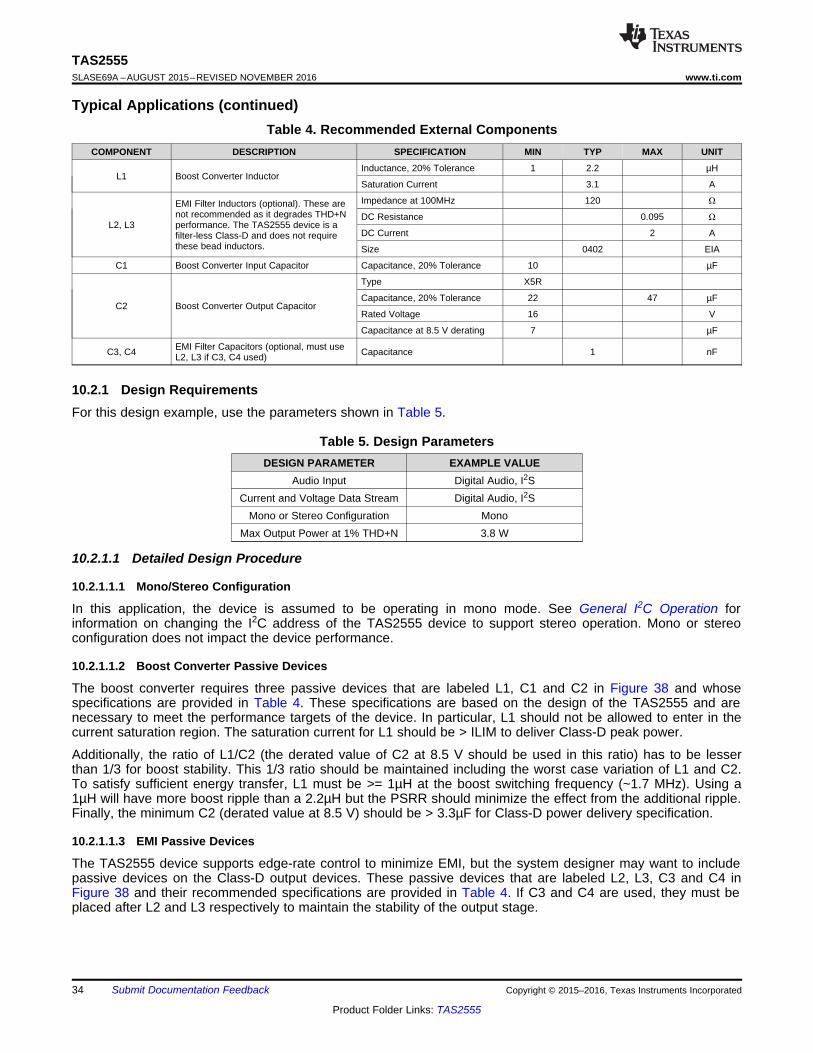
34
TAS2555SLASE69A –AUGUST 2015–REVISED NOVEMBER 2016 www.ti.com
Product Folder Links: TAS2555
Submit Documentation Feedback Copyright © 2015–2016, Texas Instruments Incorporated
Typical Applications (continued)Table 4. Recommended External Components
COMPONENT DESCRIPTION SPECIFICATION MIN TYP MAX UNIT
L1 Boost Converter InductorInductance, 20% Tolerance 1 2.2 µH
Saturation Current 3.1 A
L2, L3
EMI Filter Inductors (optional). These arenot recommended as it degrades THD+Nperformance. The TAS2555 device is afilter-less Class-D and does not requirethese bead inductors.
Impedance at 100MHz 120 Ω
DC Resistance 0.095 Ω
DC Current 2 A
Size 0402 EIA
C1 Boost Converter Input Capacitor Capacitance, 20% Tolerance 10 µF
C2 Boost Converter Output Capacitor
Type X5R
Capacitance, 20% Tolerance 22 47 µF
Rated Voltage 16 V
Capacitance at 8.5 V derating 7 µF
C3, C4 EMI Filter Capacitors (optional, must useL2, L3 if C3, C4 used) Capacitance 1 nF
10.2.1 Design RequirementsFor this design example, use the parameters shown in Table 5.
Table 5. Design ParametersDESIGN PARAMETER EXAMPLE VALUE
Audio Input Digital Audio, I2SCurrent and Voltage Data Stream Digital Audio, I2S
Mono or Stereo Configuration MonoMax Output Power at 1% THD+N 3.8 W
10.2.1.1 Detailed Design Procedure
10.2.1.1.1 Mono/Stereo Configuration
In this application, the device is assumed to be operating in mono mode. See General I2C Operation forinformation on changing the I2C address of the TAS2555 device to support stereo operation. Mono or stereoconfiguration does not impact the device performance.
10.2.1.1.2 Boost Converter Passive Devices
The boost converter requires three passive devices that are labeled L1, C1 and C2 in Figure 38 and whosespecifications are provided in Table 4. These specifications are based on the design of the TAS2555 and arenecessary to meet the performance targets of the device. In particular, L1 should not be allowed to enter in thecurrent saturation region. The saturation current for L1 should be > ILIM to deliver Class-D peak power.
Additionally, the ratio of L1/C2 (the derated value of C2 at 8.5 V should be used in this ratio) has to be lesserthan 1/3 for boost stability. This 1/3 ratio should be maintained including the worst case variation of L1 and C2.To satisfy sufficient energy transfer, L1 must be >= 1µH at the boost switching frequency (~1.7 MHz). Using a1µH will have more boost ripple than a 2.2µH but the PSRR should minimize the effect from the additional ripple.Finally, the minimum C2 (derated value at 8.5 V) should be > 3.3µF for Class-D power delivery specification.
10.2.1.1.3 EMI Passive Devices
The TAS2555 device supports edge-rate control to minimize EMI, but the system designer may want to includepassive devices on the Class-D output devices. These passive devices that are labeled L2, L3, C3 and C4 inFigure 38 and their recommended specifications are provided in Table 4. If C3 and C4 are used, they must beplaced after L2 and L3 respectively to maintain the stability of the output stage.
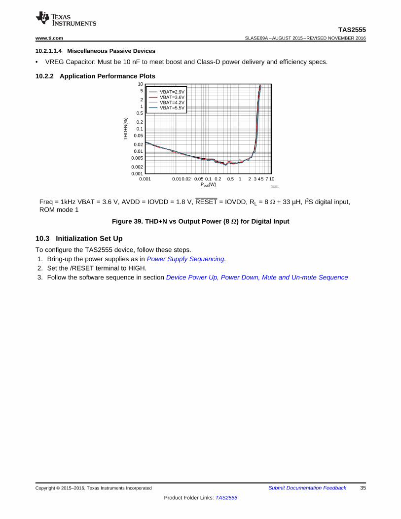
Pout(W)
TH
D+
N(%
)
0.001 0.010.02 0.05 0.1 0.2 0.5 1 2 3 45 7 100.001
0.002
0.005
0.010.02
0.05
0.1
0.2
0.5
1
2
510
D001
VBAT=2.9VVBAT=3.6VVBAT=4.2VVBAT=5.5V
35
TAS2555www.ti.com SLASE69A –AUGUST 2015–REVISED NOVEMBER 2016
Product Folder Links: TAS2555
Submit Documentation FeedbackCopyright © 2015–2016, Texas Instruments Incorporated
10.2.1.1.4 Miscellaneous Passive Devices
• VREG Capacitor: Must be 10 nF to meet boost and Class-D power delivery and efficiency specs.
10.2.2 Application Performance Plots
Freq = 1kHz VBAT = 3.6 V, AVDD = IOVDD = 1.8 V, RESET = IOVDD, RL = 8 Ω + 33 µH, I2S digital input,ROM mode 1
Figure 39. THD+N vs Output Power (8 Ω) for Digital Input
10.3 Initialization Set UpTo configure the TAS2555 device, follow these steps.1. Bring-up the power supplies as in Power Supply Sequencing.2. Set the /RESET terminal to HIGH.3. Follow the software sequence in section Device Power Up, Power Down, Mute and Un-mute Sequence

Tdelay >= 0s
Tdelay >= 0s
Tdelay >= 0s
VBAT
IOVDD
DVDD
AVDD
Tdelay >= 0s
Tdelay >= 0s
Tdelay >= 0s
36
TAS2555SLASE69A –AUGUST 2015–REVISED NOVEMBER 2016 www.ti.com
Product Folder Links: TAS2555
Submit Documentation Feedback Copyright © 2015–2016, Texas Instruments Incorporated
11 Power Supply Recommendations
11.1 Power SuppliesThe TAS2555 device requires four power supplies:• Boost Input (terminal: VBAT)
– Voltage: 2.9 V to 5.5 V– Max Current: 5 A for ILIM = 3.0 A (default)
• Analog Supply (terminal: AVDD)– Voltage: 1.65 V to 1.95 V– Max Current: 30 mA
• Digital Supply (terminal: DVDD)– Voltage: 1.65 V to 1.95 V– Max Current: 40 mA
• Digital I/O Supply (terminal: IOVDD)– Voltage: 1.62 V to 3.6 V– Max Current: 5 mA
The decoupling capacitors for the power supplies should be placed close to the device terminals. For VBAT,IOVDD, DVDD and AVDD, a small decoupling capacitor of 0.1 µF should be placed close to the device terminals.Refer to for the schematic.
11.2 Power Supply SequencingThe following power sequence should be followed for power up and power down. If the recommended sequenceis not followed there can be large current in device due to faults in level shifters and diodes becoming forwardbiased. The Tdelay between power supplies should be large enough for the power rails to settle.
Figure 40. Power Supply Sequence for Power-Up and Power-Down
When the supplies have settled, the /RESET terminal can be set HIGH to operate the device. Additionally the/RESET pin can be tied to IOVDD and the internal DVDD POR will perform a reset of the device. After ahardware or software reset additional commands to the device should be delayed for 100uS to allow the OTP toload. The above sequence should be completed before any I2C operation.
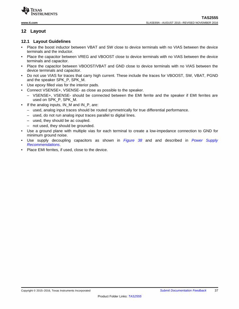
37
TAS2555www.ti.com SLASE69A –AUGUST 2015–REVISED NOVEMBER 2016
Product Folder Links: TAS2555
Submit Documentation FeedbackCopyright © 2015–2016, Texas Instruments Incorporated
12 Layout
12.1 Layout Guidelines• Place the boost inductor between VBAT and SW close to device terminals with no VIAS between the device
terminals and the inductor.• Place the capacitor between VREG and VBOOST close to device terminals with no VIAS between the device
terminals and capacitor.• Place the capacitor between VBOOST/VBAT and GND close to device terminals with no VIAS between the
device terminals and capacitor.• Do not use VIAS for traces that carry high current. These include the traces for VBOOST, SW, VBAT, PGND
and the speaker SPK_P, SPK_M.• Use epoxy filled vias for the interior pads.• Connect VSENSE+, VSENSE- as close as possible to the speaker.
– VSENSE+, VSENSE- should be connected between the EMI ferrite and the speaker if EMI ferrites areused on SPK_P, SPK_M.
• If the analog inputs, IN_M and IN_P, are:– used, analog input traces should be routed symmetrically for true differential performance.– used, do not run analog input traces parallel to digital lines.– used, they should be ac coupled.– not used, they should be grounded.
• Use a ground plane with multiple vias for each terminal to create a low-impedance connection to GND forminimum ground noise.
• Use supply decoupling capacitors as shown in Figure 38 and and described in Power SupplyRecommendations.
• Place EMI ferrites, if used, close to the device.

BOOST
CAPACITOR
GROUND PLANE
GND
A
B
C
D
E
6 5 4 3 2
G
F
1
BOOST
INDUCTORVBAT
SPK_M
SPK_P
GND
FERRITE
BEAD
FERRITE
BEAD
VBAT DECOUPLING
CAPACITOR
VBAT
GND
VIA-IN-PAD
VIA TO GND PLANE
TWO INTERNAL
GND PLANES
38
TAS2555SLASE69A –AUGUST 2015–REVISED NOVEMBER 2016 www.ti.com
Product Folder Links: TAS2555
Submit Documentation Feedback Copyright © 2015–2016, Texas Instruments Incorporated
12.2 Layout Example
Figure 41. TAS2555 Board Layout

39
TAS2555www.ti.com SLASE69A –AUGUST 2015–REVISED NOVEMBER 2016
Product Folder Links: TAS2555
Submit Documentation FeedbackCopyright © 2015–2016, Texas Instruments Incorporated
13 Register Map
See the General I2C Operation section for more details on addressing. Register settings should be set based onthe files generated from the PPC3 GUI. Because the TAS2555 device is a complex system including the internalsoftware, changes made in the TAS2555 registers not known in the PPC3 generated configurations can result inthe speaker protection not operating correctly. Changes should be made from within PurePath™ Console 3Software TAS2555 Application instead of manually changing registers when possible. New configuration files canbe generated from PPC3 to prevent invalid configurations.
13.1 Register Map Summary
Table 6. Summary of Register MapDecimal Hex DESCRIPTION
BOOKNO.
PAGENO.
REG.NO.
BOOKNO.
PAGENO.
REG.NO.
0 0 0 0x00 0x00 0x00 Page Select0 0 1 0x00 0x00 0x01 Software Reset0 0 2-3 0x00 0x00 0x02-
0x03Reserved
0 0 4 0x00 0x00 0x04 Power Control0 0 5 0x00 0x00 0x05 Power Control 20 0 6 0x00 0x00 0x06 Speaker Control0 0 7 0x00 0x00 0x07 Mute0 0 8 0x00 0x00 0x08 Channel Control0 0 9-31 0x00 0x00 0x09-
0x1FReserved
0 0 32 0x00 0x00 0x20 CRC Checksum0 0 33 0x00 0x00 0x21 Checksum Reset0 0 34 0x00 0x00 0x22 Device DSP Mode0 0 35-39 0x00 0x00 0x23-
0x27Reserved
0 0 40 0x00 0x00 0x28 Class-D SSM Mode0 0 41 0x00 0x00 0x29 Reserved0 0 42 0x00 0x00 0x2A Digital Playback Control0 0 43 0x00 0x00 0x2B Current Limit0 0 44 0x00 0x00 0x2C Clock Error Control 10 0 45 0x00 0x00 0x2D Clock Error Control 20 0 46 0x00 0x00 0x2E Clock Error Control 30 0 47-99 0x00 0x00 0x2F-
0x63Reserved
0 0 100 0x00 0x00 0x64 Power Up Flag0 0 101-103 0x00 0x00 0x65-
0x67Reserved
0 0 104 0x00 0x00 0x68 Interrupt Flags DAC & OCP/OTP Sticky0 0 105-107 0x00 0x00 0x69-
0x6BReserved
0 0 108 0x00 0x00 0x6C DSP Interrupt Output Sticky0 0 109-120 0x00 0x00 0x6D-
0x78Reserved
0 0 121 0x00 0x00 0x79 Power Modes0 0 122-126 0x00 0x00 0x7A-
0x7EReserved
0 0 127 0x00 0x00 0x7F Book Selection0 1 0 0x00 0x01 0x00 Page Select

40
TAS2555SLASE69A –AUGUST 2015–REVISED NOVEMBER 2016 www.ti.com
Product Folder Links: TAS2555
Submit Documentation Feedback Copyright © 2015–2016, Texas Instruments Incorporated
Register Map Summary (continued)Table 6. Summary of Register Map (continued)
Decimal Hex DESCRIPTIONBOOKNO.
PAGENO.
REG.NO.
BOOKNO.
PAGENO.
REG.NO.
0 1 1 0x00 0x01 0x01 ASI1 DAC Format0 1 2 0x00 0x01 0x02 ASI1 ADC Format0 1 3 0x00 0x01 0x03 ASI1 Offset0 1 4-6 0x00 0x01 0x04-
0x06Reserved
0 1 7 0x00 0x01 0x07 ASI1 ADC Path0 1 8 0x00 0x01 0x08 ASI1 DAC BCLK0 1 9 0x00 0x01 0x09 ASI1 DAC WCLK0 1 10 0x00 0x01 0x0A ASI1 ADC BCLK0 1 11 0x00 0x01 0x0B ASI1 ADC WCLK0 1 12 0x00 0x01 0x0C ASI1 DIN/DOUT MUX0 1 13 0x00 0x01 0x0D ASI1 BDIV Clock Select0 1 14 0x00 0x01 0x0E ASI1 BDIV Clock Ratio0 1 15 0x00 0x01 0x0F ASI1 WDIV Clock Ratio0 1 16 0x00 0x01 0x10 ASI1 DAC Clock Output0 1 17 0x00 0x01 0x11 ASI1 ADC Clock Output0 1 18-20 0x00 0x01 0x12-
0x14Reserved
0 1 21 0x00 0x01 0x15 ASI2 DAC Format0 1 22 0x00 0x01 0x16 ASI2 ADC Format0 1 23 0x00 0x01 0x17 ASI2 Offset0 1 24-26 0x00 0x01 0x18-
0x1AReserved
0 1 27 0x00 0x01 0x1B ASI2 ADC Path0 1 28 0x00 0x01 0x1C ASI2 DAC BCLK0 1 29 0x00 0x01 0x1D ASI2 DAC WCLK0 1 30 0x00 0x01 0x1E ASI2 ADC BCLK0 1 31 0x00 0x01 0x1F ASI2 ADC WCLK0 1 32 0x00 0x01 0x20 ASI2 DIN/DOUT MUX0 1 33 0x00 0x01 0x21 ASI2 BDIV Clock Select0 1 34 0x00 0x01 0x22 ASI2 BDIV Clock Ratio0 1 35 0x00 0x01 0x23 ASI2 WDIV Clock Ratio0 1 36 0x00 0x01 0x24 ASI2 DAC Clock Output0 1 37 0x00 0x01 0x25 ASI2 ADC Clock Output0 1 38-60 0x00 0x01 0x26-
0x3CReserved
0 1 61 0x00 0x01 0x3D BCLK1_GPIO1 Pin0 1 62 0x00 0x01 0x3E WCLK1_GPIO2 Pin0 1 63 0x00 0x01 0x3F DOUT1_GPIO3 Pin0 1 64 0x00 0x01 0x40 IRQ_GPIO4 Pin0 1 65 0x00 0x01 0x41 BCLK2_GPIO5 Pin0 1 66 0x00 0x01 0x42 WCLK2_GPIO6 Pinb0 1 67 0x00 0x01 0x43 DOUT2_GPIO7 Pin0 1 68 0x00 0x01 0x44 DIN2_GPIO8 Pin0 1 69 0x00 0x01 0x45 ICC_CLK_GPIO9 Pin

41
TAS2555www.ti.com SLASE69A –AUGUST 2015–REVISED NOVEMBER 2016
Product Folder Links: TAS2555
Submit Documentation FeedbackCopyright © 2015–2016, Texas Instruments Incorporated
Register Map Summary (continued)Table 6. Summary of Register Map (continued)
Decimal Hex DESCRIPTIONBOOKNO.
PAGENO.
REG.NO.
BOOKNO.
PAGENO.
REG.NO.
0 1 70 0x00 0x01 0x46 ICC_GPIO10 Pin0 1 71-76 0x00 0x01 0x47-
0x4CReserved
0 1 77 0x00 0x01 0x4D GPI Pin0 1 78 0x00 0x01 0x4E Reserved0 1 79 0x00 0x01 0x4F GPIO HIZ CTRL10 1 80 0x00 0x01 0x50 GPIO HIZ CTRL20 1 81 0x00 0x01 0x51 GPIO HIZ CTRL30 1 82 0x00 0x01 0x52 GPIO HIZ CTRL40 1 83 0x00 0x01 0x53 GPIO HIZ CTRL30 1 84-86 0x00 0x01 0x54-
0x56Reserved
0 1 87 0x00 0x01 0x57 GPIO Pin 10 1 88 0x00 0x01 0x58 GPIO Pin 20 1 89 0x00 0x01 0x59 GPIO Pin 30 1 90-107 0x00 0x01 0x5A-
0x6BReserved
0 1 108 0x00 0x01 0x6C Interrupt Control 10 1 109 0x00 0x01 0x6D Interrupt Control 20 1 110 0x00 0x01 0x6E Interrupt Control 30 1 111 0x00 0x01 0x6F Interrupt Control 40 1 112 0x00 0x01 0x70 Interrupt Control 50 1 113 0x00 0x01 0x71 Interrupt Control 60 1 114-127 0x00 0x01 0x72-
0xFFReserved Registers
0 2 0 0x00 0x01 0x00 Page Select Register0 2 1-5 0x00 0x01 0x01-
0x05Reserved Registers
0 2 6 0x00 0x01 0x06 Ramp Generator Frequency0 2 7-23 0x00 0x01 0x07x17 Reserved Registers0 2 24 0x00 0x01 0x18 Inrush Optimization 10 2 25 0x00 0x01 0x19 Inrush Optimization 20 2 26 0x00 0x01 0x1A Inrush Optimization 30 2 27 0x00 0x01 0x1B Inrush Optimization 40 2 28-127 0x00 0x01 0x1C-
0x7FReserved Registers
100 0 0 0x64 0x00 0x00 Page Select Register100 0 1 0x64 0x00 0x01 DAC Interpolation100 0 2 0x64 0x00 0x02 ADC interpolation Register100 0 3-6 0x64 0x00 0x03-
0x06Reserved Registers
100 0 7 0x64 0x00 0x07 DSP Mute Register100 0 8-15 0x64 0x00 0x0F Reserved Registers100 0 16 0x64 0x00 0x10 Interrupt 1 DSP100 0 17 0x64 0x00 0x11 Interrupt 2 DSP100 0 18 0x64 0x00 0x12 Condition 1 DSP

42
TAS2555SLASE69A –AUGUST 2015–REVISED NOVEMBER 2016 www.ti.com
Product Folder Links: TAS2555
Submit Documentation Feedback Copyright © 2015–2016, Texas Instruments Incorporated
Register Map Summary (continued)Table 6. Summary of Register Map (continued)
Decimal Hex DESCRIPTIONBOOKNO.
PAGENO.
REG.NO.
BOOKNO.
PAGENO.
REG.NO.
100 0 19 0x64 0x00 0x13 Condition 2 DSP100 0 20 0x64 0x00 0x14 ISR and COND Control100 0 21 0x64 0x00 0x15 DSP Control Register100 0 22-26 0x64 0x00 0x16-
0x1AReserved Register
100 0 27 0x64 0x00 0x1B PLL CLKIN Divider100 0 28 0x64 0x00 0x1C PLL J-VAL Divider100 0 29 0x64 0x00 0x1D PLL D-VAL Divider 2100 0 30 0x64 0x00 0x1E D-VAL Divider 1100 0 31 0x64 0x00 0x1F DSP Clock100 0 32 0x64 0x00 0x20 N-VAL Divider100 0 33 0x64 0x00 0x21 MDAC-VAL Divider100 0 34 0x64 0x00 0x22 MADC-VAL Divider100 0 35-37 0x64 0x00 0x23-
0x25Reserved Register
100 0 38 0x64 0x00 0x26 Charge-pump Clock100 0 39 0x64 0x00 0x27 Boost Clock100 0 40 0x64 0x00 0x28 Ramp Clock 1100 0 41-42 0x64 0x00 0x29-
0x2AReserved Register
100 0 43 0x64 0x00 0x2B Ramp Clock 2100 0 44 0x64 0x00 0x2C Ramp Clock 3100 0 45-126 0x64 0x00 0x2D-
0x7EReserved Register
100 0 127 0x64 0x00 0x7F Book Selection
13.2 Book 0 Page 0
Book 0 / Page 0 / Register 0: Page Select Register - 0x00 / 0x00 / 0x00 (B0_P0_R0)
BIT FIELD READ/WRITE
RESETVALUE DESCRIPTION
D7-D0 PAGE R/W 00000000
Page Select Register0-255: Selects the Register Page for next read or write command.Refer Table for details.
Book 0 / Page 0 / Register 1: Software Reset Register - 0x00 / 0x00 / 0x01 (B0_P0_R1)
BIT FIELD READ/WRITE
RESETVALUE DESCRIPTION
D7-D1 RESERVED R/W 0000 000 Reserved. Write only reset values.D0 RESET R/W 0 Self-clearing software reset bit. Set to value of 1 to reset.
0: Don't care1: Self clearing software reset
Book 0 / Page 0 / Register 2-3: Reserved Registers - 0x00 / 0x00 / 0x02-0x03 (B0_P0_R2-3)
BIT FIELD READ/WRITE
RESETVALUE DESCRIPTION
D7-D0 RESERVED R xxxxxxxx
Reserved.
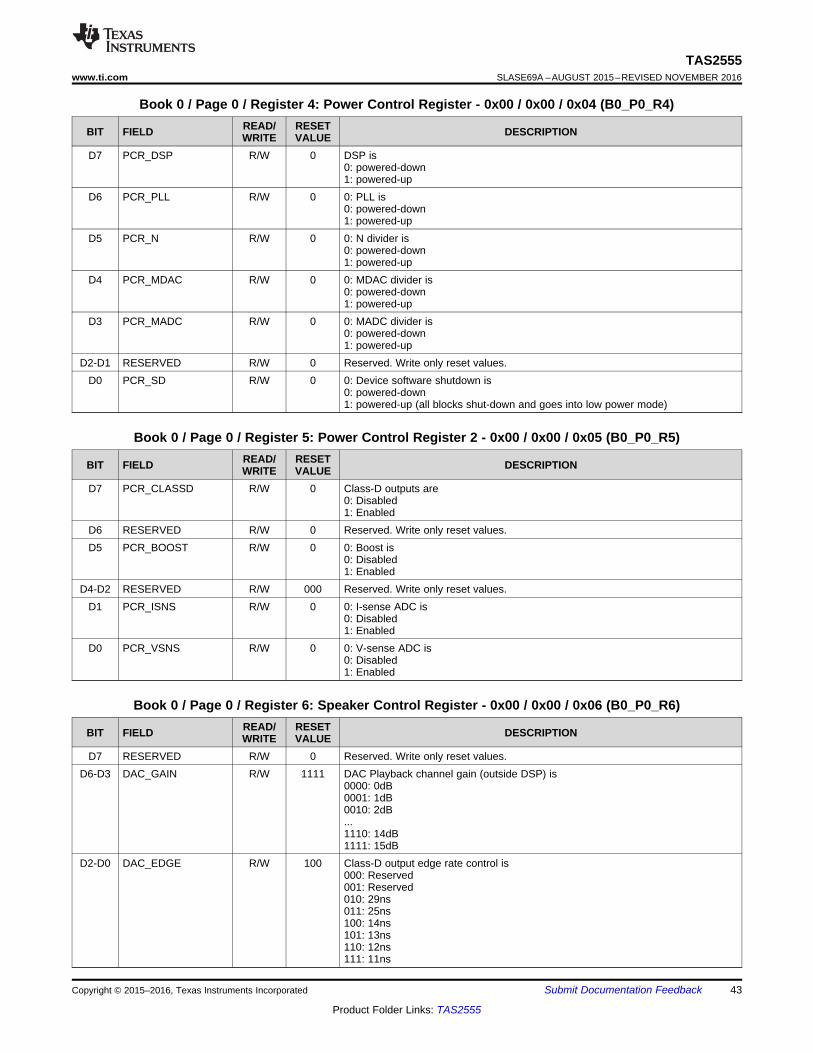
43
TAS2555www.ti.com SLASE69A –AUGUST 2015–REVISED NOVEMBER 2016
Product Folder Links: TAS2555
Submit Documentation FeedbackCopyright © 2015–2016, Texas Instruments Incorporated
Book 0 / Page 0 / Register 4: Power Control Register - 0x00 / 0x00 / 0x04 (B0_P0_R4)
BIT FIELD READ/WRITE
RESETVALUE DESCRIPTION
D7 PCR_DSP R/W 0 DSP is0: powered-down1: powered-up
D6 PCR_PLL R/W 0 0: PLL is0: powered-down1: powered-up
D5 PCR_N R/W 0 0: N divider is0: powered-down1: powered-up
D4 PCR_MDAC R/W 0 0: MDAC divider is0: powered-down1: powered-up
D3 PCR_MADC R/W 0 0: MADC divider is0: powered-down1: powered-up
D2-D1 RESERVED R/W 0 Reserved. Write only reset values.D0 PCR_SD R/W 0 0: Device software shutdown is
0: powered-down1: powered-up (all blocks shut-down and goes into low power mode)
Book 0 / Page 0 / Register 5: Power Control Register 2 - 0x00 / 0x00 / 0x05 (B0_P0_R5)
BIT FIELD READ/WRITE
RESETVALUE DESCRIPTION
D7 PCR_CLASSD R/W 0 Class-D outputs are0: Disabled1: Enabled
D6 RESERVED R/W 0 Reserved. Write only reset values.D5 PCR_BOOST R/W 0 0: Boost is
0: Disabled1: Enabled
D4-D2 RESERVED R/W 000 Reserved. Write only reset values.D1 PCR_ISNS R/W 0 0: I-sense ADC is
0: Disabled1: Enabled
D0 PCR_VSNS R/W 0 0: V-sense ADC is0: Disabled1: Enabled
Book 0 / Page 0 / Register 6: Speaker Control Register - 0x00 / 0x00 / 0x06 (B0_P0_R6)
BIT FIELD READ/WRITE
RESETVALUE DESCRIPTION
D7 RESERVED R/W 0 Reserved. Write only reset values.D6-D3 DAC_GAIN R/W 1111 DAC Playback channel gain (outside DSP) is
0000: 0dB0001: 1dB0010: 2dB...1110: 14dB1111: 15dB
D2-D0 DAC_EDGE R/W 100 Class-D output edge rate control is000: Reserved001: Reserved010: 29ns011: 25ns100: 14ns101: 13ns110: 12ns111: 11ns

44
TAS2555SLASE69A –AUGUST 2015–REVISED NOVEMBER 2016 www.ti.com
Product Folder Links: TAS2555
Submit Documentation Feedback Copyright © 2015–2016, Texas Instruments Incorporated
Book 0 / Page 0 / Register 7: Mute Register - 0x00 / 0x00 / 0x07 (B0_P0_R7)
BIT FIELD READ/WRITE
RESETVALUE DESCRIPTION
D7-D5 RESERVED R/W 000 Reserved. Write only reset values.D4-D2 RESERVED R/W 000 Reserved. Write only reset values.
D1 MUTE_ISNS R/W 1 0: Un-mute I-sense1: Mute I-sense
D0 MUTE_SPK R/W 1 0: Un-mute Class-D1: Mute Class-D
Book 0 / Page 0 / Register 8: Channel Control Register - 0x00 / 0x00 / 0x08 (B0_P0_R8)
BIT FIELD READ/WRITE
RESETVALUE DESCRIPTION
D7-D3 RESERVED R/W 00000 Reserved. Write only reset values.D2-D1 SENSE_GAIN R/W 00 IVsense gain setting is
00: Isense channel full-scale output corresponds to 1.25A and Vsense channel full-scale output corresponds to 8.5V (recommended to use for 8-ohm )01: Isense channel full-scale output corresponds to 1.48A and Vsense channel full-scale output corresponds to 8.5V (recommended to use for 6-ohm load case)10: Isense channel full-scale output corresponds to 1.76A and Vsense channel full-scale output corresponds to 8.5V (recommended to use for 4-ohm load case)11: Reserved
D0 VSENSE_ADCM R/W 0 Vsense ADC is used for0: sensing Class-D output voltage1: analog input
Book 0 / Page 0 / Register 9-31: Reserved Registers - 0x00 / 0x00 / 0x09-0x1F (B0_P0_R9-31)
BIT FIELD READ/WRITE
RESETVALUE DESCRIPTION
D7-D0 RESERVED R xxxxxxxx
Reserved
Book 0 / Page 0 / Register 32: CRC Checksum Register - 0x00 / 0x00 / 0x20 (B0_P0_R32)
BIT FIELD READ/WRITE
RESETVALUE DESCRIPTION
D7-D0 CRC_CHECKSUM R xxxxxxxx
CRC checksum of all encrypted PRAM content downloaded to device sincechecksum reset
Book 0 / Page 0 / Register 33: Checksum Reset Register - 0x00 / 0x00 / 0x21 (B0_P0_R33)
BIT FIELD READ/WRITE
RESETVALUE DESCRIPTION
D7-D1 RESERVED R/W 000 0000 Reserved. Write only reset values.D0 CRC_RESET R/W 0 PRAM Checksum
0: PRAM download check-sum is not reset.1: PRAM download check-sum is reset. (This is recommended to be done beforePRAM code download so that after download the above checksum value can beread to confirm download process has any error )
Book 0 / Page 0 / Register 34: Device DSP Mode Register - 0x00 / 0x00 / 0x22 (B0_P0_R34)
BIT FIELD READ/WRITE
RESETVALUE DESCRIPTION
D7-D6 RESERVED R/W 00 Reserved. Write only reset values.D5 MODE_COEFF R/W 1 Default coefficients are
0: from host. Host needs to download coefficients into device.1: from internal ROM. Default coefficients for ROM modes.
D4-D2 RESERVED R/W 000 Reserved. Write only reset values.

45
TAS2555www.ti.com SLASE69A –AUGUST 2015–REVISED NOVEMBER 2016
Product Folder Links: TAS2555
Submit Documentation FeedbackCopyright © 2015–2016, Texas Instruments Incorporated
Book 0 / Page 0 / Register 34: Device DSP Mode Register - 0x00 / 0x00 / 0x22 (B0_P0_R34) (continued)
BIT FIELD READ/WRITE
RESETVALUE DESCRIPTION
D1-D0 MODE_DSP R/W 01 DSP Mode is00: SmartAmp Mode01: ROM Mode 1: Digital input playback only10: ROM Mode 2: Digital input with I/V-sense11: Reserved
Book 0 / Page 0 / Register 35-39: Reserved Registers - 0x00 / 0x00 / 0x23-0x27 (B0_P0_R35-R39)
BIT FIELD READ/WRITE
RESETVALUE DESCRIPTION
D7-D0 RESERVED R xxxxxxxx
Reserved
Book 0 / Page 0 / Register 40: Class-D SSM Mode Register - 0x00 / 0x00 / 0x28 (B0_P0_R40)
BIT FIELD READ/WRITE
RESETVALUE DESCRIPTION
D7-D1 RESERVED R/W 000 0000 Reserved. Write only default values.D0 RAMP_SSM_MODE R/W 0 Ramp generator Spread Spectrum Mode (SSM) mode of operation is
0: Disabled.1: Enabled. This is supported only when Class-D RAMP_CLK is generated usingon-chip RAMP CLK generator, which can be configured using B100_P0_R40.
Book 0 / Page 0 / Register 41: Reserved Registers - 0x00 / 0x00 / 0x29 (B0_P0_R41)
BIT FIELD READ/WRITE
RESETVALUE DESCRIPTION
D7-D0 RESERVED R xxxxxxxx
Reserved
Book 0 / Page 0 / Register 42: Digital Playback Control Register - 0x00 / 0x00 / 0x2A (B0_P0_R42)
BIT FIELD READ/WRITE
RESETVALUE DESCRIPTION
D7-D5 RESERVED R/W 000 Reserved. Write only reset values.D4-D3 ASI2_CHANNEL R/W 0 ASI2 Playback Input
00: ASI2 Left channel is used01: ASI2 Right channel is used10: ASI2 (Left+Right)/2 is used11: ASI2 monoPCM input expected
D2-D1 ASI1_CHANNEL R/W 0 ASI1 Playback Input00: ASI1 Left channel is used01: ASI1 Right channel is used10: ASI1 (Left+Right)/2 is used11: ASI1 monoPCM input expected
D0 SOFT_MUTE R/W 0 Soft Stepping of Mute/Un-Mute is0: Enabled1: Disabled
Book 0 / Page 0 / Register 43: Current Limit Register - 0x00 / 0x00 / 0x2B (B0_P0_R43)
BIT FIELD READ/WRITE
RESETVALUE DESCRIPTION
D7-D2 RESERVED R/W 0000 00 Reserved. Write only reset values.D1-D0 BOOST_ILIMIT R/W 11 Boost current limit is
00: 1.5A01: 2.0A10: 2.5A11: 3.0A

46
TAS2555SLASE69A –AUGUST 2015–REVISED NOVEMBER 2016 www.ti.com
Product Folder Links: TAS2555
Submit Documentation Feedback Copyright © 2015–2016, Texas Instruments Incorporated
Book 0 / Page 0 / Register 44: Clock Error Control 1 Register - 0x00 / 0x00 / 0x2C (B0_P0_R44)
BIT FIELD READ/WRITE
RESETVALUE DESCRIPTION
D7-D5 RESERVED R 000 Reserved. Write only reset values.D4 CLK_ERR1_INPUT R/W 0 Clock error detection 1 input clock is
0: ASI11: ASI2
D3-D2 CLK_ERR2_INPUT R/W 00 Clock error detection 2 input clock is00: DAC modulator clock01: ADC modulator clock10: PLL clock11: Reserved
D1 CLK_ERR1_EN R/W 0 Clock error detection 1 is0: Disable1: Enable
D0 CLK_ERR2_EN R/W 0 Clock error detection 2 is0: Disable1: Enable
Book 0 / Page 0 / Register 45: Clock Error Control 2 Register - 0x00 / 0x00 / 0x2D (B0_P0_R45)
BIT FIELD READ/WRITE
RESETVALUE DESCRIPTION
D7-D3 RESERVED R 0001 0 Reserved. Write only reset values.D2-D0 CLK_ERR1_TO R/W 111 Clock error detection 1 shutdown timeout. B0_P0_R4[0] will be 1 after shutdown.
Program that bit to 0 before powering up the device again. Chip will shutdown if avalid clock is not applied to error detection1 block for000: 11ms001: 22ms010: 44ms011: 87ms100: 174ms101: 350ms110: 700ms111: 1.4s
Book 0 / Page 0 / Register 46: Clock Error Control 3 Register - 0x00 / 0x00 / 0x2E (B0_P0_R46)
BIT FIELD READ/WRITE
RESETVALUE DESCRIPTION
D7-D3 RESERVED R 0001 0 Reserved. Write only reset values.D2-D0 CLK_ERR2_TO R/W 111 Clock error detection 2 shutdown timeout. B0_P0_R4[0] will be 1 after shutdown.
Program that bit to 0 before powering up the device again. Chip will shutdown if avalid clock is not applied to error detection2 block for000: 11ms001: 22ms010: 44ms011: 87ms100: 174ms101: 350ms110: 700ms111: 1.4s
Book 0 / Page 0 / Register 47-99: Reserved Registers - 0x00 / 0x00 / 0x2F-0x63 (B0_P0_R47-R99)
BIT FIELD READ/WRITE
RESETVALUE DESCRIPTION
D7-D0 RESERVED R xxxxxxxx
Reserved

47
TAS2555www.ti.com SLASE69A –AUGUST 2015–REVISED NOVEMBER 2016
Product Folder Links: TAS2555
Submit Documentation FeedbackCopyright © 2015–2016, Texas Instruments Incorporated
Book 0 / Page 0 / Register 100: Power Up Flag Register - 0x00 / 0x00 / 0x64 (B0_P0_R100)
BIT FIELD READ/WRITE
RESETVALUE DESCRIPTION
D7 PWR_DAC R 0 DAC Power is0: DAC Powered Down1: DAC Powered Up
D6 PWR_SPK R 0 Class D Power is0: Class D Powered Down1: Class D Powered Up
D5 PWR_BOOST R 0 Boost Power is0: Boost Powered Down1: Boost Powered Up
D4 BOOST_PT_EN R 0 Boost Pass-through is0: Boost Pass-through disable1: Boost Pass-through enable
D3 PWR_ISENSE R 0 ISense ADC Power is0: ISense ADC Powered Down1: ISense ADC Powered Up
D2 PWR_VSENSE R 0 VSense ADC Power is0: VSense ADC Powered Down1: VSense ADC Powered Up
D1-D0 RESERVED R 00 Reserved
Book 0 / Page 0 / Register 101-103: Reserved Registers - 0x00 / 0x00 / 0x65-0x67 (B0_P0_R101-R103)
BIT FIELD READ/WRITE
RESETVALUE DESCRIPTION
D7-D0 RESERVED R xxxxxxxx
Reserved
Book 0 / Page 0 / Register 104: Interrupt Flags DAC & OCP/OTP Sticky Register - 0x00 / 0x00 / 0x68(B0_P0_R104)
BIT FIELD READ/WRITE
RESETVALUE DESCRIPTION
D7 OVER_CURRENT R 0 SPK Over-current STICKY - Cleared once read is0: SPK Over-current is not detected1: SPK Over-current is detected
D6 UNDER_VOLTAGE R 0 SPK Over-voltage STICKY - Cleared once read is0: Analog supplies under voltage is not detected1: Analog supplies under voltage is detected
D5 RESERVED R 0 ReservedD4 OVER_TEMP R 0 Over-temperature STICKY - Cleared once read is
0: Over-temperature is not detected1: Over-temperature is detected
D3 BROWNOUT R 0 Brownout STICKY - Cleared once read is0: Normal supply is present1: Brownout condition is detected
D2 CLK_PRESENT R 0 Clock Present STICKY - Cleared once read is0: Clock is present1: Clock is lost
D1 SAR_COMPLETE R 0 SAR complete STICKY - Cleared once read is0: SAR has not completed1: SAR complete
D0 RESERVED R 0 Reserved
Book 0 / Page 0 / Register 105-107: Reserved Registers - 0x00 / 0x00 / 0x69-0x6B (B0_P0_R105-R107)
BIT FIELD READ/WRITE
RESETVALUE DESCRIPTION
D7-D0 RESERVED R xxxxxxxx
Reserved
48
TAS2555SLASE69A –AUGUST 2015–REVISED NOVEMBER 2016 www.ti.com
Product Folder Links: TAS2555
Submit Documentation Feedback Copyright © 2015–2016, Texas Instruments Incorporated
Book 0 / Page 0 / Register 108: DSP Interrupt Output Sticky Register - 0x00 / 0x00 / 0x6C (B0_P0_R108)
BIT FIELD READ/WRITE
RESETVALUE DESCRIPTION
D7 INT1 R 0 DSP output Interrupt1 Port Output STICKY - Cleared once readD6 INT2 R 0 DSP output Interrupt2 Port Output STICKY - Cleared once readD5 INT3 R 0 DSP output Interrupt3 Port Output STICKY - Cleared once readD4 INT4 R 0 DSP output Interrupt4 Port Output STICKY - Cleared once read
D3-D0 RESERVED R 0000 Reserved
Book 0 / Page 0 / Register 109-120: Reserved Registers - 0x00 / 0x00 / 0x6D-0x78 (B0_P0_R109-R120)
BIT FIELD READ/WRITE
RESETVALUE DESCRIPTION
D7-D0 RESERVED R xxxxxxxx
Reserved
Book 0 / Page 0 / Register 121: Power Modes Register - 0x00 / 0x00 / 0x79 (B0_P0_R121)
BIT FIELD READ/WRITE
RESETVALUE DESCRIPTION
D7 LOW_POWER_EN R/W 0 Low-power sleep mode is0: Disabled1: Enabled - Set high only when AVDD and VBAT supplies are available in thesystem.
D6-D0 RESERVED R/W 000 0000 Reserved. Write only reset values.
Book 0 / Page 0 / Register 122-126: Reserved Registers - 0x00 / 0x00 / 0x7A-0x7E (B0_P0_R122-R126)
BIT FIELD READ/WRITE
RESETVALUE DESCRIPTION
D7-D0 RESERVED R xxxxxxxx
Reserved
Book 0 / Page 0 / Register 127: Book Selection Register - 0x00 / 0x00 / 0x7F (B0_P0_R127)
BIT FIELD READ/WRITE
RESETVALUE DESCRIPTION
D7-D0 BOOK R/W 00000000
0-255: Selects the Register Book for next read or write command.
13.3 Book 0 Page 1
Book 0 / Page 1 / Register 0: Page Select Register - 0x00 / 0x01 / 0x00 (B0_P1_R0)
BIT FIELD READ/WRITE
RESETVALUE DESCRIPTION
D7-D0 PAGE R/W 00000001
Page Select Register is0-255: Selects the Register Page for next read or write command.Refer Table for details.
Book 0 / Page 1 / Register 1: ASI1 DAC Format Register - 0x00 / 0x01 / 0x01 (B0_P1_R1)
BIT FIELD READ/WRITE
RESETVALUE DESCRIPTION
D7-D5 ASI1D_INTERFACE R/W 000 ASI1 DAC interface is000: I2S001: DSP010: Right-Justified (RJF). Non-zero values of ASI1_OFFSET1 not supported.011: Left-Justified (LJF)100: MonoPCM101-111: Reserved

49
TAS2555www.ti.com SLASE69A –AUGUST 2015–REVISED NOVEMBER 2016
Product Folder Links: TAS2555
Submit Documentation FeedbackCopyright © 2015–2016, Texas Instruments Incorporated
Book 0 / Page 1 / Register 1: ASI1 DAC Format Register - 0x00 / 0x01 / 0x01 (B0_P1_R1) (continued)
BIT FIELD READ/WRITE
RESETVALUE DESCRIPTION
D4-D3 ASI1D_WORD_LEN R/W 10 ASI1 DAC word length is00: 16 bits01: 20 bits10: 24 bits11: 32 bits
D2-D1 RESERVED R/W 00 Reserved. Write only reset values.D0 ASI1_TRISTATE R/W 0 Tri-stating of DOUT1 for the extra ASI1_BCLK cycles after Data Transfer is over
for a frame is0: Disabled1: Enabled
Book 0 / Page 1 / Register 2: ASI1 ADC Format Register - 0x00 / 0x01 / 0x02 (B0_P1_R2)
BIT FIELD READ/WRITE
RESETVALUE DESCRIPTION
D7-D5 ASI1A_INTERFACE R/W 000 ASI1 ADC Interface (This register control is valid only if D0 = 1)000: I2S001: DSP010: RJF. non-zero values of ASI1_OFFSET1 not supported.011: LJF100: MonoPCM101-111: Reserved
D4-D3 ASI1A_WORD_LEN R/W 00 ASI1 ADC word length (This register control is valid only if D0 = 1)00: 16 bits01: 20 bits10: 24 bits11: 32 bits
D2-D1 RESERVED R/W 00 Reserved. Write only reset values.D0 ASI1A_USE_DAC R/W 0 ASI1 ADC uses
0: the same Interface type and word length as DAC side as in B0_P1_R11: the Interface type and word length from B0_P1_R2[7:3]
Book 0 / Page 1 / Register 3: ASI1 Offset Register - 0x00 / 0x00 / 0x03 (B0_P1_R3)
BIT FIELD READ/WRITE
RESETVALUE DESCRIPTION
D7-D0 ASI1_OFFSET R/W 00000000
ASI1_OFFSET = x ASI1_BCLK's. Offset is measured with respect to WCLK-risingedge in DSP Mode. Offset is not supported for RJF mode0000 0000: 0 ASI1_BCLK's0000 0001: 1 ASI1_BCLK's...1111 1110: 254 ASI1_BCLK's1111 1111: 255 ASI1_BCLK's
Book 0 / Page 1 / Register 4-6: Reserved Registers - 0x00 / 0x01 / 0x04-0x06 (B0_P1_R4-6)
BIT FIELD READ/WRITE
RESETVALUE DESCRIPTION
D7-D0 RESERVED R xxxxxxxx
Reserved.
Book 0 / Page 1 / Register 7: ASI1 ADC Path Register - 0x00 / 0x01 / 0x07 (B0_P1_R7)
BIT FIELD READ/WRITE
RESETVALUE DESCRIPTION
D7-D3 RESERVED R/W 0000 0 Reserved. Write only reset values.

50
TAS2555SLASE69A –AUGUST 2015–REVISED NOVEMBER 2016 www.ti.com
Product Folder Links: TAS2555
Submit Documentation Feedback Copyright © 2015–2016, Texas Instruments Incorporated
Book 0 / Page 1 / Register 7: ASI1 ADC Path Register - 0x00 / 0x01 / 0x07 (B0_P1_R7) (continued)
BIT FIELD READ/WRITE
RESETVALUE DESCRIPTION
D2-D0 ASI1A_PATH R/W 001 ASI1 ADC path is000: ASI1_ADC_DATA is disabled. No serial data output from ASI1001: ASI1_ADC_DATA <Left,Right> = DSP_OUT<Left,Right>010: Reserved011: Reserved100: Reserved101: ASI1_ADC_DATA<Left,Right> = ASI1_CHANNEL<Left,Right>110: ASI1_ADC_DATA<L1,R1> = ASI2_CHANNEL<Left,Right>111: Reserved
Book 0 / Page 1 / Register 8: ASI1 DAC BCLK Register - 0x00 / 0x01 / 0x08 (B0_P1_R8)
BIT FIELD READ/WRITE
RESETVALUE DESCRIPTION
D7 RESERVED R/W 0 Reserved. Write only reset values.D6-D3 ASI1D_BCLK_PATH R/W 0000 ASI1_DAC_BCLK input from
0000: GPIO1 (Preferred pin usage)0001: GPIO20010: GPIO30011: GPIO40100: GPIO50101: GPIO60110: GPIO70111: GPIO81000: GPIO91001: GPIO101010: Reserved1011: Reserved1100: GPI11101: GPI21110: GPI31111: Reserved
D2 RESERVED R/W 0 Reserved. Write only reset values.D1 ASI1D_BCLK_EDGE R/W 0 ASI1_DAC_BCLK timing per protocol is
0: normal1: inverted
D0 AS1_BWCLK_MODE R/W 0 ASI1 BCLK /WCLK output mode0: ASI1_DAC_BCLK and ASI1_DAC_WCLK are active in output modes only whenASI1 is active and/or codec is powered up1: ASI1_DAC_BCLK and ASI1_DAC_WCLK are free running.
Book 0 / Page 1 / Register 9: ASI1 DAC WCLK Register - 0x00 / 0x01 / 0x09 (B0_P1_R9)
BIT FIELD READ/WRITE
RESETVALUE DESCRIPTION
D7 RESERVED R/W 0 Reserved. Write only reset values.D6-D3 ASI1D_WCLK_PATH R/W 0001 ASI1_DAC_WCLK input from
0000: GPIO10001: GPIO2 (Preferred pin usage)0010: GPIO30011: GPIO40100: GPIO50101: GPIO60110: GPIO70111: GPIO81000: GPIO91001: GPIO101010: Reserved1011: Reserved1100: GPI11101: GPI21110: GPI31111: Reserved
51
TAS2555www.ti.com SLASE69A –AUGUST 2015–REVISED NOVEMBER 2016
Product Folder Links: TAS2555
Submit Documentation FeedbackCopyright © 2015–2016, Texas Instruments Incorporated
Book 0 / Page 1 / Register 9: ASI1 DAC WCLK Register - 0x00 / 0x01 / 0x09 (B0_P1_R9) (continued)
BIT FIELD READ/WRITE
RESETVALUE DESCRIPTION
D2 RESERVED R/W 0 Reserved. Write only reset values.D1 ASI1D_WCLK_EDGE R/W 0 ASI1_DAC_WCLK timing per protocol
0: normal1: inverted
D0 RESERVED R/W 0 Reserved. Write only reset values.
Book 0 / Page 1 / Register 10: ASI1 ADC BCLK Register - 0x00 / 0x01 / 0x0A (B0_P1_R10)
BIT FIELD READ/WRITE
RESETVALUE DESCRIPTION
D7 RESERVED R/W 0 Reserved. Write only reset values.D6-D3 ASI1A_BCLK_PATH R/W 1111 ASI1_ADC_BCLK input from
0000: GPIO10001: GPIO20010: GPIO30011: GPIO40100: GPIO50101: GPIO60110: GPIO70111: GPIO81000: GPIO91001: GPIO101010: Reserved1011: Reserved1100: GPI11101: GPI21110: GPI31111: ASI1_DAC_BCLK_PATH B0_P1_R8[6:3] (Preferred usage)
D2 RESERVED R/W 0 Reserved. Write only reset values.D1 ASI1A_BCLK_EDGE R/W 0 ASI1_ADC_BCLK timing per protocol is
0: normal1: inverted
D0 RESERVED R/W 0 Reserved. Write only reset values.
Book 0 / Page 1 / Register 11: ASI1 ADC WCLK Register - 0x00 / 0x01 / 0x0B (B0_P1_R11)
BIT FIELD READ/WRITE
RESETVALUE DESCRIPTION
D7 RESERVED R/W 0 Reserved. Write only reset values.D6-D3 ASI1A_WCLK_PATH R/W 1111 ASI1_ADC_WCLK input from
0000: GPIO10001: GPIO20010: GPIO30011: GPIO40100: GPIO50101: GPIO60110: GPIO70111: GPIO81000: GPIO91001: GPIO101010: Reserved1011: Reserved1100: GPI11101: GPI21110: GPI31111: ASI1_ADC_WCLK_PATH B0_P1_R9[6:3] (Preferred usage)
D2 RESERVED R/W 0 Reserved. Write only reset values.D1 ASI1A_WCLK_EDGE R/W 0 ASI1_ADC_WCLK timing per protocol is
0: normal1: inverted
D0 RESERVED R/W 0 Reserved. Write only reset values.

52
TAS2555SLASE69A –AUGUST 2015–REVISED NOVEMBER 2016 www.ti.com
Product Folder Links: TAS2555
Submit Documentation Feedback Copyright © 2015–2016, Texas Instruments Incorporated
Book 0 / Page 1 / Register 12: ASI1 DIN/DOUT MUX Register - 0x00 / 0x01 / 0x0C (B0_P1_R12)
BIT FIELD READ/WRITE
RESETVALUE DESCRIPTION
D7 RESERVED R/W 0 Reserved. Write only reset values.D6-D3 ASI1_DIN_PATH R/W 1100 ASI1_DIN input from
0000: GPIO10001: GPIO20010: GPIO30011: GPIO40100: GPIO50101: GPIO60110: GPIO70111: GPIO81000: GPIO91001: GPIO101010: Reserved1011: Reserved1100: GPI1 (Preferred pin usage)1101: GPI21110: GPI31111: Reserved
D2 RESERVED R/W 0 Reserved. Write only reset values.D1-D0 ASI1_DOUT_PATH R/W 00 ASI1_DOUT output from
00: Direct DOUT path (pin to pin loopback disabled)01: ASI1_DIN ( Pin to Pin Loopback )10: ASI2_DIN ( Pin to Pin Loopback )11: Reserved
Book 0 / Page 1 / Register 13: ASI1 BDIV Clock Select Register - 0x00 / 0x01 / 0x0D (B0_P1_R13)
BIT FIELD READ/WRITE
RESETVALUE DESCRIPTION
D7-D3 RESERVED R/W 0000 0 Reserved. Write only reset values.D2-D0 ASI1_BDIV_CLKIN R/W 001 ASI1_BDIV_CLKIN is
000: NDIV_CLK (Generated On-Chip)001: DAC_MOD_CLK (Generated On-Chip)010: Reserved011: ADC_MOD_CLK (Generated On-Chip)100: ASI1_DAC_BCLK (at pin)101: ASI1_ADC_BCLK (at pin)110: ASI2_DAC_BCLK (at pin)111: ASI2_ADC_BCLK (at pin)
Book 0 / Page 1 / Register 14: ASI1 BDIV Clock Ratio Register - 0x00 / 0x01 / 0x0E (B0_P1_R14)
BIT FIELD READ/WRITE
RESETVALUE DESCRIPTION
D7 ASI1_BDIV_PWR R/W 0 ASI1_BDIV divider is0: powered down1: powered up
D6-D0 ASI1_BDIV_RATIO R/W 000 0010 ASI1_BDIV000 0000: 128000 0001: 1000 0010: 2...111 1110: 126111 1111: 127
Book 0 / Page 1 / Register 15: ASI1 WDIV Clock Ratio Register - 0x00 / 0x01 / 0x0F (B0_P1_R15)
BIT FIELD READ/WRITE
RESETVALUE DESCRIPTION
D7 ASI1_WDIV_PWR R/W 0 ASI1_WDIV divider is0: powered down1: powered up

53
TAS2555www.ti.com SLASE69A –AUGUST 2015–REVISED NOVEMBER 2016
Product Folder Links: TAS2555
Submit Documentation FeedbackCopyright © 2015–2016, Texas Instruments Incorporated
Book 0 / Page 1 / Register 15: ASI1 WDIV Clock Ratio Register - 0x00 / 0x01 / 0x0F(B0_P1_R15) (continued)
BIT FIELD READ/WRITE
RESETVALUE DESCRIPTION
D6-D0 ASI1_WDIV_RATIO R/W 010 0000 ASI1_WDIV000 0000: 128000 0001: 1...010 0000 :32...111 1110: 126111 1111: 127
Book 0 / Page 1 / Register 16: ASI1 DAC Clock Output Register - 0x00 / 0x01 / 0x10 (B0_P1_R16)
BIT FIELD READ/WRITE
RESETVALUE DESCRIPTION
D7 RESERVED R/W 0 Reserved. Write only reset values.D6-D4 ASI1D_BCLK_OUT R/W 000 ASI1_DAC_BCLK_OUT
000: ASI1_BDIV_OUT001: ASI1_DAC_BCLK010: ASI1_ADC_BCLK011: ASI2_BDIV_OUT100: ASI2_DAC_BCLK101: ASI2_ADC_BCLK110: Reserved111: Reserved
D3 RESERVED R/W 0 Reserved. Write only reset values.D2-D0 ASI1D_WCLK_OUT R/W 001 ASI1_DAC_WCLK_OUT
000: ASI1_WDIV_OUT001: ASI1_DAC_WCLK010: ASI1_ADC_WCLK011: ASI2_WDIV_OUT100: ASI2_DAC_WCLK101: ASI2_ADC_WCLK110: Reserved111: Reserved
Book 0 / Page 1 / Register 17: ASI1 ADC Clock Output Register - 0x00 / 0x01 / 0x11 (B0_P1_R17)
BIT FIELD READ/WRITE
RESETVALUE DESCRIPTION
D7 RESERVED R/W 0 Reserved. Write only reset values.D6-D4 ASI1A_BCLK_OUT R/W 000 ASI1_ADC_BCLK_OUT
000: ASI1_BDIV_OUT001: ASI1_DAC_BCLK010: ASI1_ADC_BCLK011: ASI2_BDIV_OUT100: ASI2_DAC_BCLK101: ASI2_ADC_BCLK110: Reserved111: Reserved
D3 RESERVED R/W 0 Reserved. Write only reset values.D2-D0 ASI1A_WCLK_OUT R/W 001 ASI1_ADC_WCLK_OUT
000: ASI1_WDIV_OUT001: ASI1_DAC_WCLK010: ASI1_ADC_WCLK011: ASI2_WDIV_OUT100: ASI2_DAC_WCLK101: ASI2_ADC_WCLK110: Reserved111: Reserved
54
TAS2555SLASE69A –AUGUST 2015–REVISED NOVEMBER 2016 www.ti.com
Product Folder Links: TAS2555
Submit Documentation Feedback Copyright © 2015–2016, Texas Instruments Incorporated
Book 0 / Page 1 / Register 18-20: Reserved Registers - 0x00 / 0x01 / 0x12-0x14 (B0_P1_R18-20)
BIT FIELD READ/WRITE
RESETVALUE DESCRIPTION
D7-D0 RESERVED R xxxxxxxx
Reserved.
Book 0 / Page 1 / Register 21: ASI2 DAC Format Register - 0x00 / 0x01 / 0x15 (B0_P1_R21)
BIT FIELD READ/WRITE
RESETVALUE DESCRIPTION
D7-D5 ASI2D_INTERFACE R/W 000 ASI2 DAC interface is000: I2S001: DSP010: Right Justified (RJF). Non-zero values of ASI2_OFFSET not supported.011: Left Justified (LJF)100: MonoPCM101-111: Reserved
D4-D3 ASI2D_WORD_LEN R/W 10 ASI2 DAC word length is00: 16 bits01: 20 bits10: 24 bits11: 32 bits
D2-D1 RESERVED R/W 00 Reserved. Write only reset values.D0 ASI2_TRISTATE R/W 0 Tristating of DOUT1 for the extra ASI2_BCLK cycles after Data Transfer is over for
a frame0: Disabled1: Enabled
Book 0 / Page 1 / Register 22: ASI2 ADC Format Register - 0x00 / 0x01 / 0x16 (B0_P1_R22)
BIT FIELD READ/WRITE
RESETVALUE DESCRIPTION
D7-D5 ASI2A_INTERFACE R/W 000 ASI2 ADC interface is (This register control is valid only if D0 = 1)000: I2S001: DSP010: Right Justified (RJF). Non-zero values of ASI2_OFFSET not supported.011: Left Justified (LJF)100: MonoPCM101-111: Reserved
D4-D3 ASI2A_WORD_LEN R/W 00 ASI2 ADC word length is (This register control is valid only if D0 = 1)00: 16 bits01: 20 bits10: 24 bits11: 32 bits
D2-D1 RESERVED R/W 00 Reserved. Write only reset values.D0 ASI2A_USE_DAC R/W 0 ASI2 ADC uses
0: the same Interface type and word length as DAC side as in B0_P1_R11: the Interface type and word length from B0_P1_R2[7:3]
Book 0 / Page 1 / Register 23: ASI2 Offset Register - 0x00 / 0x01 / 0x17 (B0_P1_R23)
BIT FIELD READ/WRITE
RESETVALUE DESCRIPTION
D7-D0 ASI2_OFFSET R/W 00000000
ASI2_OFFSET = x ASI2_BCLK's. Offset is measured with respect to WCLK-risingedge in DSP Mode. Offset is not supported for RJF mode0000 0000: 0 ASI2_BCLK's0000 0001: 1 ASI2_BCLK's...1111 1110: 254 ASI2_BCLK's1111 1111: 255 ASI2_BCLK's
55
TAS2555www.ti.com SLASE69A –AUGUST 2015–REVISED NOVEMBER 2016
Product Folder Links: TAS2555
Submit Documentation FeedbackCopyright © 2015–2016, Texas Instruments Incorporated
Book 0 / Page 1 / Register 24-26: Reserved Registers - 0x00 / 0x01 / 0x18-0x1A (B0_P1_R24-26)
BIT FIELD READ/WRITE
RESETVALUE DESCRIPTION
D7-D0 RESERVED R xxxxxxxx
Reserved.
Book 0 / Page 1 / Register 27: ASI2 ADC Path Register - 0x00 / 0x01 / 0x1B (B0_P1_R27)
BIT FIELD READ/WRITE
RESETVALUE DESCRIPTION
D7-D3 RESERVED R 0000 0 Reserved. Write only reset values.D2-D0 ASI2A_PATH R/W 010 ASI2 ADC Path is
000: ASI2_ADC_DATA is disabled. No serial data output from ASI2001: Reserved010: ASI2_ADC_DATA <Left,Right> = DSP_OUT<Left,Right>011: Reserved100: Reserved101: ASI1_ADC_DATA<Left,Right> = ASI1_CHANNEL<Left,Right>110: ASI1_ADC_DATA<Left,Right> = ASI2_CHANNEL<Left,Right>111: Reserved
Book 0 / Page 1 / Register 28: ASI2 DAC BCLK Register - 0x00 / 0x01 / 0x1C (B0_P1_R28)
BIT FIELD READ/WRITE
RESETVALUE DESCRIPTION
D7 RESERVED R/W 0 Reserved. Write only reset values.D6-D3 ASI2D_BCLK_PATH R/W 0100 ASI1_DAC_BCLK input from
0000: GPIO10001: GPIO20010: GPIO30011: GPIO40100: GPIO5 (Preferred pin usage)0101: GPIO60110: GPIO70111: GPIO81000: GPIO91001: GPIO101010: Reserved1011: Reserved1100: GPI11101: GPI21110: GPI31111: Reserved
D2 RESERVED R/W 0 Reserved. Write only reset values.D1 ASI2D_BCLK_EDGE R/W 0 ASI2_DAC_BCLK timing per protocol is
0: normal1: inverted
D0 ASI2_BWCLK_MODE R/W 0 ASI2 BCLK /WCLK output mode is0: ASI2_DAC_BCLK and ASI2_DAC_WCLK are active in output modes only whenASI2 is active and/or codec is powered up1: ASI2_DAC_BCLK and ASI2_DAC_WCLK are free running.
Book 0 / Page 1 / Register 29: ASI2 DAC WCLK Register - 0x00 / 0x01 / 0x1D (B0_P1_R29)
BIT FIELD READ/WRITE
RESETVALUE DESCRIPTION
D7 RESERVED R/W 0 Reserved. Write only reset values.

56
TAS2555SLASE69A –AUGUST 2015–REVISED NOVEMBER 2016 www.ti.com
Product Folder Links: TAS2555
Submit Documentation Feedback Copyright © 2015–2016, Texas Instruments Incorporated
Book 0 / Page 1 / Register 29: ASI2 DAC WCLK Register - 0x00 / 0x01 / 0x1D (B0_P1_R29) (continued)
BIT FIELD READ/WRITE
RESETVALUE DESCRIPTION
D6-D3 ASI2_WCLK_PATH R/W 0101 ASI2_DAC_WCLK input from0000: GPIO10001: GPIO20010: GPIO30011: GPIO40100: GPIO50101: GPIO6 (Preferred pin usage)0110: GPIO70111: GPIO81000: GPIO91001: GPIO101010: Reserved1011: Reserved1100: GPI11101: GPI21110: GPI31111: Reserved
D2 RESERVED R/W 0 Reserved. Write only reset values.D1 ASI2D_WCLK_EDGE R/W 0 ASI2_DAC_WCLK timing per protocol is
0: normal1: inverted
D0 RESERVED R/W 0 Reserved. Write only reset values.
Book 0 / Page 1 / Register 30: ASI2 ADC BCLK Register - 0x00 / 0x01 / 0x1E (B0_P1_R30)
BIT FIELD READ/WRITE
RESETVALUE DESCRIPTION
D7 RESERVED R/W 0 Reserved. Write only reset values.D6-D3 ASI2A_BCLK_PATH R/W 1111 ASI2_ADC_BCLK input from
0000: GPIO10001: GPIO20010: GPIO30011: GPIO40100: GPIO50101: GPIO60110: GPIO70111: GPIO81000: GPIO91001: GPIO101010: Reserved1011: Reserved1100: GPI11101: GPI21110: GPI31111: ASI2_DAC_BCLK_PATH B0_P1_R28[6:3] (Preferred usage)
D2 RESERVED R/W 0 Reserved. Write only reset values.D1 ASI2A_BCLK_EDGE R/W 0 ASI2_ADC_BCLK timing per protocol is
0: normal1: inverted
D0 RESERVED R/W 0 Reserved. Write only reset values.
Book 0 / Page 1 / Register 31: ASI2 ADC WCLK Register - 0x00 / 0x01 / 0x1F (B0_P1_R31)
BIT FIELD READ/WRITE
RESETVALUE DESCRIPTION
D7 RESERVED R/W 0 Reserved. Write only reset values.
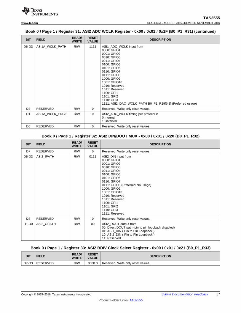
57
TAS2555www.ti.com SLASE69A –AUGUST 2015–REVISED NOVEMBER 2016
Product Folder Links: TAS2555
Submit Documentation FeedbackCopyright © 2015–2016, Texas Instruments Incorporated
Book 0 / Page 1 / Register 31: ASI2 ADC WCLK Register - 0x00 / 0x01 / 0x1F (B0_P1_R31) (continued)
BIT FIELD READ/WRITE
RESETVALUE DESCRIPTION
D6-D3 ASI1A_WCLK_PATH R/W 1111 ASI1_ADC_WCLK input from0000: GPIO10001: GPIO20010: GPIO30011: GPIO40100: GPIO50101: GPIO60110: GPIO70111: GPIO81000: GPIO91001: GPIO101010: Reserved1011: Reserved1100: GPI11101: GPI21110: GPI31111: ASI2_DAC_WCLK_PATH B0_P1_R29[6:3] (Preferred usage)
D2 RESERVED R/W 0 Reserved. Write only reset values.D1 ASI1A_WCLK_EDGE R/W 0 ASI2_ADC_WCLK timing per protocol is
0: normal1: inverted
D0 RESERVED R/W 0 Reserved. Write only reset values.
Book 0 / Page 1 / Register 32: ASI2 DIN/DOUT MUX - 0x00 / 0x01 / 0x20 (B0_P1_R32)
BIT FIELD READ/WRITE
RESETVALUE DESCRIPTION
D7 RESERVED R/W 0 Reserved. Write only reset values.D6-D3 ASI2_IPATH R/W 0111 ASI2_DIN input from
0000: GPIO10001: GPIO20010: GPIO30011: GPIO40100: GPIO50101: GPIO60110: GPIO70111: GPIO8 (Preferred pin usage)1000: GPIO91001: GPIO101010: Reserved1011: Reserved1100: GPI11101: GPI21110: GPI31111: Reserved
D2 RESERVED R/W 0 Reserved. Write only reset values.D1-D0 ASI2_OPATH R/W 00 ASI2_DOUT output from
00: Direct DOUT path (pin to pin loopback disabled)01: ASI1_DIN ( Pin to Pin Loopback )10: ASI2_DIN ( Pin to Pin Loopback )11: Reserved
Book 0 / Page 1 / Register 33: ASI2 BDIV Clock Select Register - 0x00 / 0x01 / 0x21 (B0_P1_R33)
BIT FIELD READ/WRITE
RESETVALUE DESCRIPTION
D7-D3 RESERVED R/W 0000 0 Reserved. Write only reset values.

58
TAS2555SLASE69A –AUGUST 2015–REVISED NOVEMBER 2016 www.ti.com
Product Folder Links: TAS2555
Submit Documentation Feedback Copyright © 2015–2016, Texas Instruments Incorporated
Book 0 / Page 1 / Register 33: ASI2 BDIV Clock Select Register - 0x00 / 0x01 / 0x21(B0_P1_R33) (continued)
BIT FIELD READ/WRITE
RESETVALUE DESCRIPTION
D2-D0 ASI1_BDIV_CLKIN R/W 001 ASI2_BDIV_CLKIN000: NDIV_CLK (Generated On-Chip)001: DAC_MOD_CLK (Generated On-Chip)010: Reserved011: ADC_MOD_CLK (Generated On-Chip)100: ASI1_DAC_BCLK (at pin)101: ASI1_ADC_BCLK (at pin)110: ASI2_DAC_BCLK (at pin)111: ASI2_ADC_BCLK (at pin)
Book 0 / Page 1 / Register 34: ASI2 BDIV Clock Ratio Register - 0x00 / 0x01 / 0x22 (B0_P1_R34)
BIT FIELD READ/WRITE
RESETVALUE DESCRIPTION
D7 ASI2_BDIV_PWR R/W 0 ASI2_BDIV divider is0: powered down1: powered up
D6-D0 ASI2_BDIV_RTO R/W 000 0010 ASI2_BDIV000 0000: 128000 0001: 1000 0010: 2...111 1110: 126111 1111: 127
Book 0 / Page 1 / Register 35: ASI2 WDIV Clock Ratio Register - 0x00 / 0x01 / 0x23 (B0_P1_R35)
BIT FIELD READ/WRITE
RESETVALUE DESCRIPTION
D7 ASI2_WDIV_PWR R/W 0 ASI2_WDIV divider is0: powered down1: powered up
D6-D0 ASI2_WDIV_RTO R/W 010 0000 ASI2_BDIV Ratio000 0000: 128000 0001: 1...010 0000 :32...111 1110: 126111 1111: 127
Book 0 / Page 1 / Register 36: ASI2 DAC Clock Output Register - 0x00 / 0x01 / 0x24 (B0_P1_R36)
BIT FIELD READ/WRITE
RESETVALUE DESCRIPTION
D7 RESERVED R/W 0 Reserved. Write only reset values.D6-D4 ASI2D_BCLKO R/W 011 ASI2_DAC_BCLK_OUT
000: ASI1_BDIV_OUT001: ASI1_DAC_BCLK010: ASI1_ADC_BCLK011: ASI2_BDIV_OUT100: ASI2_DAC_BCLK101: ASI2_ADC_BCLK110: Reserved111: Reserved
D3 RESERVED R/W 0 Reserved. Write only reset values.
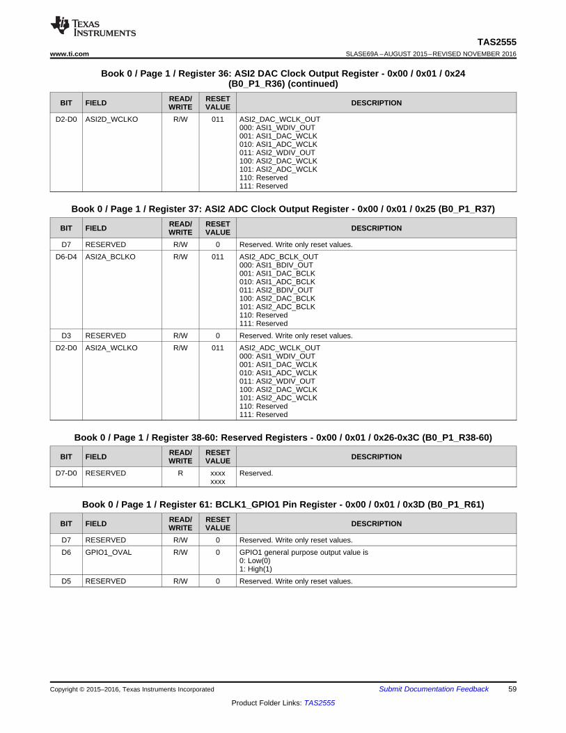
59
TAS2555www.ti.com SLASE69A –AUGUST 2015–REVISED NOVEMBER 2016
Product Folder Links: TAS2555
Submit Documentation FeedbackCopyright © 2015–2016, Texas Instruments Incorporated
Book 0 / Page 1 / Register 36: ASI2 DAC Clock Output Register - 0x00 / 0x01 / 0x24(B0_P1_R36) (continued)
BIT FIELD READ/WRITE
RESETVALUE DESCRIPTION
D2-D0 ASI2D_WCLKO R/W 011 ASI2_DAC_WCLK_OUT000: ASI1_WDIV_OUT001: ASI1_DAC_WCLK010: ASI1_ADC_WCLK011: ASI2_WDIV_OUT100: ASI2_DAC_WCLK101: ASI2_ADC_WCLK110: Reserved111: Reserved
Book 0 / Page 1 / Register 37: ASI2 ADC Clock Output Register - 0x00 / 0x01 / 0x25 (B0_P1_R37)
BIT FIELD READ/WRITE
RESETVALUE DESCRIPTION
D7 RESERVED R/W 0 Reserved. Write only reset values.D6-D4 ASI2A_BCLKO R/W 011 ASI2_ADC_BCLK_OUT
000: ASI1_BDIV_OUT001: ASI1_DAC_BCLK010: ASI1_ADC_BCLK011: ASI2_BDIV_OUT100: ASI2_DAC_BCLK101: ASI2_ADC_BCLK110: Reserved111: Reserved
D3 RESERVED R/W 0 Reserved. Write only reset values.D2-D0 ASI2A_WCLKO R/W 011 ASI2_ADC_WCLK_OUT
000: ASI1_WDIV_OUT001: ASI1_DAC_WCLK010: ASI1_ADC_WCLK011: ASI2_WDIV_OUT100: ASI2_DAC_WCLK101: ASI2_ADC_WCLK110: Reserved111: Reserved
Book 0 / Page 1 / Register 38-60: Reserved Registers - 0x00 / 0x01 / 0x26-0x3C (B0_P1_R38-60)
BIT FIELD READ/WRITE
RESETVALUE DESCRIPTION
D7-D0 RESERVED R xxxxxxxx
Reserved.
Book 0 / Page 1 / Register 61: BCLK1_GPIO1 Pin Register - 0x00 / 0x01 / 0x3D (B0_P1_R61)
BIT FIELD READ/WRITE
RESETVALUE DESCRIPTION
D7 RESERVED R/W 0 Reserved. Write only reset values.D6 GPIO1_OVAL R/W 0 GPIO1 general purpose output value is
0: Low(0)1: High(1)
D5 RESERVED R/W 0 Reserved. Write only reset values.

60
TAS2555SLASE69A –AUGUST 2015–REVISED NOVEMBER 2016 www.ti.com
Product Folder Links: TAS2555
Submit Documentation Feedback Copyright © 2015–2016, Texas Instruments Incorporated
Book 0 / Page 1 / Register 61: BCLK1_GPIO1 Pin Register - 0x00 / 0x01 / 0x3D (B0_P1_R61) (continued)
BIT FIELD READ/WRITE
RESETVALUE DESCRIPTION
D4-D0 GPIO1_FUNCT R/W 0 0001 Pin BCLK1_GPIO1 function is0 0000: Disabled (Input and Output buffers powered down)0 0001: Input mode0 0010: Reserved0 0011: Output = General Purpose Output level set by bit D60 0100: Output = General Purpose Output level set by B0_P1_R88 & B0_P1_R870 0101: Output = Reserved0 0110: Output = CLKOUT Output0 0111: Output = INT1 Interrupt Output0 1000: Output = INT2 Interrupt Output0 1001: Output = INT3 Interrupt Output0 1010: Output = INT4 Interrupt Output0 1011: Reserved0 1100: Output = ASI1 word clock output0 1101: Output = ASI1 bit clock output0 1110: Output = ASI1_WCLK_ADC_OUT0 1111: Output = ASI1_BCLK_ADC_OUT1 0000: Output = ASI1_DOUT1 0001: Output = ASI2_WCLK_OUT1 0010: Output = ASI2_BCLK_OUT1 0011: Output = ASI2_WCLK_ADC_OUT1 0100: Output = ASI2_BCLK_ADC_OUT1 0101: Output = ASI2_DOUT1 0110: Output = ASIM_WCLK_OUT1 0111: Output = ASIM_BCLK_OUT1 1000: Output = ASIM_DOUT1 1001: Reserved...1 1111: Reserved
Book 0 / Page 1 / Register 62: WCLK1_GPIO2 Pin Register - 0x00 / 0x01 / 0x3E (B0_P1_R62)
BIT FIELD READ/WRITE
RESETVALUE DESCRIPTION
D7 RESERVED R/W 0 Reserved. Write only reset values.D6 GPIO2_OVAL R/W 0 GPIO2 general purpose output value is
0: Low(0)1: High(1)
D5 RESERVED R/W 0 Reserved. Write only reset values.

61
TAS2555www.ti.com SLASE69A –AUGUST 2015–REVISED NOVEMBER 2016
Product Folder Links: TAS2555
Submit Documentation FeedbackCopyright © 2015–2016, Texas Instruments Incorporated
Book 0 / Page 1 / Register 62: WCLK1_GPIO2 Pin Register - 0x00 / 0x01 / 0x3E (B0_P1_R62) (continued)
BIT FIELD READ/WRITE
RESETVALUE DESCRIPTION
D4-D0 GPIO2_FUNC R/W 0 0001 Pin WCLK1_GPIO2 function is0 0000: Disabled (Input and Output buffers powered down)0 0001: Input mode0 0010: Reserved0 0011: Output = General Purpose Output level set by bit D60 0100: Output = General Purpose Output level set by B0_P1_R88 & B0_P1_R870 0101: Output = Reserved0 0110: Output = CLKOUT Output0 0111: Output = INT1 Interrupt Output0 1000: Output = INT2 Interrupt Output0 1001: Output = INT3 Interrupt Output0 1010: Output = INT4 Interrupt Output0 1011: Reserved0 1100: Output = ASI1_WCLK_OUT0 1101: Output = ASI1_BCLK_OUT0 1110: Output = ASI1_WCLK_ADC_OUT0 1111: Output = ASI1_BCLK_ADC_OUT1 0000: Output = ASI1_DOUT1 0001: Output = ASI2_WCLK_OUT1 0010: Output = ASI2_BCLK_OUT1 0011: Output = ASI2_WCLK_ADC_OUT1 0100: Output = ASI2_BCLK_ADC_OUT1 0101: Output = ASI2_DOUT1 0110: Output = ASIM_WCLK_OUT1 0111: Output = ASIM_BCLK_OUT1 1000: Output = ASIM_DOUT1 1001: Reserved...1 1111: Reserved
Book 0 / Page 1 / Register 63: DOUT1_GPIO3 Pin Register - 0x00 / 0x01 / 0x3F (B0_P1_R63)
BIT FIELD READ/WRITE
RESETVALUE DESCRIPTION
D7 RESERVED R/W 0 Reserved. Write only reset values.D6 GPIO3_OVAL R/W 0 GPIO3 general purpose output value is
0: Low(0)1: High(1)
D5 RESERVED R/W 0 Reserved. Write only reset values.
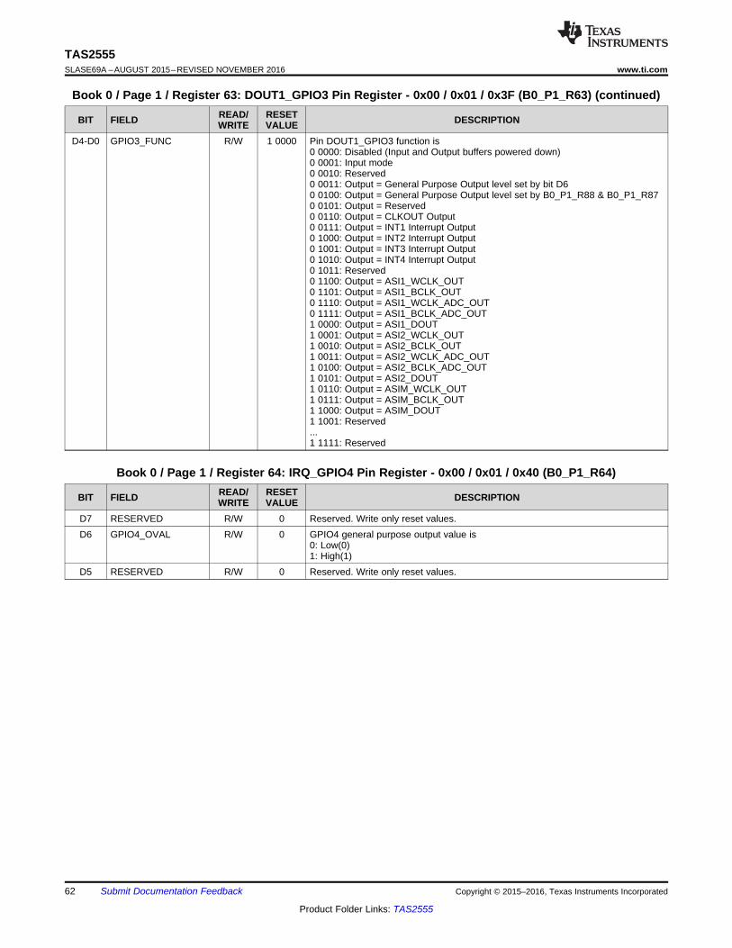
62
TAS2555SLASE69A –AUGUST 2015–REVISED NOVEMBER 2016 www.ti.com
Product Folder Links: TAS2555
Submit Documentation Feedback Copyright © 2015–2016, Texas Instruments Incorporated
Book 0 / Page 1 / Register 63: DOUT1_GPIO3 Pin Register - 0x00 / 0x01 / 0x3F (B0_P1_R63) (continued)
BIT FIELD READ/WRITE
RESETVALUE DESCRIPTION
D4-D0 GPIO3_FUNC R/W 1 0000 Pin DOUT1_GPIO3 function is0 0000: Disabled (Input and Output buffers powered down)0 0001: Input mode0 0010: Reserved0 0011: Output = General Purpose Output level set by bit D60 0100: Output = General Purpose Output level set by B0_P1_R88 & B0_P1_R870 0101: Output = Reserved0 0110: Output = CLKOUT Output0 0111: Output = INT1 Interrupt Output0 1000: Output = INT2 Interrupt Output0 1001: Output = INT3 Interrupt Output0 1010: Output = INT4 Interrupt Output0 1011: Reserved0 1100: Output = ASI1_WCLK_OUT0 1101: Output = ASI1_BCLK_OUT0 1110: Output = ASI1_WCLK_ADC_OUT0 1111: Output = ASI1_BCLK_ADC_OUT1 0000: Output = ASI1_DOUT1 0001: Output = ASI2_WCLK_OUT1 0010: Output = ASI2_BCLK_OUT1 0011: Output = ASI2_WCLK_ADC_OUT1 0100: Output = ASI2_BCLK_ADC_OUT1 0101: Output = ASI2_DOUT1 0110: Output = ASIM_WCLK_OUT1 0111: Output = ASIM_BCLK_OUT1 1000: Output = ASIM_DOUT1 1001: Reserved...1 1111: Reserved
Book 0 / Page 1 / Register 64: IRQ_GPIO4 Pin Register - 0x00 / 0x01 / 0x40 (B0_P1_R64)
BIT FIELD READ/WRITE
RESETVALUE DESCRIPTION
D7 RESERVED R/W 0 Reserved. Write only reset values.D6 GPIO4_OVAL R/W 0 GPIO4 general purpose output value is
0: Low(0)1: High(1)
D5 RESERVED R/W 0 Reserved. Write only reset values.

63
TAS2555www.ti.com SLASE69A –AUGUST 2015–REVISED NOVEMBER 2016
Product Folder Links: TAS2555
Submit Documentation FeedbackCopyright © 2015–2016, Texas Instruments Incorporated
Book 0 / Page 1 / Register 64: IRQ_GPIO4 Pin Register - 0x00 / 0x01 / 0x40 (B0_P1_R64) (continued)
BIT FIELD READ/WRITE
RESETVALUE DESCRIPTION
D4-D0 GPIO4_FUNC R/W 0 0111 Pin IRQ_GPIO4 function is0 0000: Disabled (Input and Output buffers powered down)0 0001: Input mode0 0010: Reserved0 0011: Output = General Purpose Output level set by bit D60 0100: Output = General Purpose Output level set by B0_P1_R88 & B0_P1_R870 0101: Output = Reserved0 0110: Output = CLKOUT Output0 0111: Output = INT1 Interrupt Output0 1000: Output = INT2 Interrupt Output0 1001: Output = INT3 Interrupt Output0 1010: Output = INT4 Interrupt Output0 1011: Reserved0 1100: Output = ASI1_WCLK_OUT0 1101: Output = ASI1_BCLK_OUT0 1110: Output = ASI1_WCLK_ADC_OUT0 1111: Output = ASI1_BCLK_ADC_OUT1 0000: Output = ASI1_DOUT1 0001: Output = ASI2_WCLK_OUT1 0010: Output = ASI2_BCLK_OUT1 0011: Output = ASI2_WCLK_ADC_OUT1 0100: Output = ASI2_BCLK_ADC_OUT1 0101: Output = ASI2_DOUT1 0110: Output = ASIM_WCLK_OUT1 0111: Output = ASIM_BCLK_OUT1 1000: Output = ASIM_DOUT1 1001: Reserved...1 1111: Reserved
Book 0 / Page 1 / Register 65: BCLK2_GPIO5 Pin Register - 0x00 / 0x01 / 0x41 (B0_P1_R65)
BIT FIELD READ/WRITE
RESETVALUE DESCRIPTION
D7 RESERVED R/W 0 Reserved. Write only reset values.D6 GPIO5_OVAL R/W 0 GPIO5 general purpose output value is
0: Low(0)1: High(1)
D5 RESERVED R/W 0 Reserved. Write only reset values.

64
TAS2555SLASE69A –AUGUST 2015–REVISED NOVEMBER 2016 www.ti.com
Product Folder Links: TAS2555
Submit Documentation Feedback Copyright © 2015–2016, Texas Instruments Incorporated
Book 0 / Page 1 / Register 65: BCLK2_GPIO5 Pin Register - 0x00 / 0x01 / 0x41 (B0_P1_R65) (continued)
BIT FIELD READ/WRITE
RESETVALUE DESCRIPTION
D4-D0 GPIO5_FUNC R/W 0 0000 Pin BCLK2_GPIO5 function is0 0000: Disabled (Input and Output buffers powered down)0 0001: Input mode0 0010: Reserved0 0011: Output = General Purpose Output level set by bit D60 0100: Output = General Purpose Output level set by B0_P1_R88 & B0_P1_R870 0101: Output = Reserved0 0110: Output = CLKOUT Output0 0111: Output = INT1 Interrupt Output0 1000: Output = INT2 Interrupt Output0 1001: Output = INT3 Interrupt Output0 1010: Output = INT4 Interrupt Output0 1011: Reserved0 1100: Output = ASI1_WCLK_OUT0 1101: Output = ASI1_BCLK_OUT0 1110: Output = ASI1_WCLK_ADC_OUT0 1111: Output = ASI1_BCLK_ADC_OUT1 0000: Output = ASI1_DOUT1 0001: Output = ASI2_WCLK_OUT1 0010: Output = ASI2_BCLK_OUT1 0011: Output = ASI2_WCLK_ADC_OUT1 0100: Output = ASI2_BCLK_ADC_OUT1 0101: Output = ASI2_DOUT1 0110: Output = ASIM_WCLK_OUT1 0111: Output = ASIM_BCLK_OUT1 1000: Output = ASIM_DOUT1 1001: Reserved...1 1111: Reserved
Book 0 / Page 1 / Register 66: WCLK2_GPIO6 Pin Register - 0x00 / 0x01 / 0x42 (B0_P1_R66)
BIT FIELD READ/WRITE
RESETVALUE DESCRIPTION
D7 RESERVED R/W 0 Reserved. Write only reset values.D6 GPIO6_OVAL R/W 0 GPIO6 general purpose output value is
0: Low(0)1: High(1)
D5 RESERVED R/W 0 Reserved. Write only reset values.

65
TAS2555www.ti.com SLASE69A –AUGUST 2015–REVISED NOVEMBER 2016
Product Folder Links: TAS2555
Submit Documentation FeedbackCopyright © 2015–2016, Texas Instruments Incorporated
Book 0 / Page 1 / Register 66: WCLK2_GPIO6 Pin Register - 0x00 / 0x01 / 0x42 (B0_P1_R66) (continued)
BIT FIELD READ/WRITE
RESETVALUE DESCRIPTION
D4-D0 GPIO6_FUNC R/W 0 0000 Pin WCLK2_GPIO6 function is0 0000: Disabled (Input and Output buffers powered down)0 0001: Input mode0 0010: Reserved0 0011: Output = General Purpose Output level set by bit D60 0100: Output = General Purpose Output level set by B0_P1_R88 & B0_P1_R870 0101: Output = Reserved0 0110: Output = CLKOUT Output0 0111: Output = INT1 Interrupt Output0 1000: Output = INT2 Interrupt Output0 1001: Output = INT3 Interrupt Output0 1010: Output = INT4 Interrupt Output0 1011: Reserved0 1100: Output = ASI1_WCLK_OUT0 1101: Output = ASI1_BCLK_OUT0 1110: Output = ASI1_WCLK_ADC_OUT0 1111: Output = ASI1_BCLK_ADC_OUT1 0000: Output = ASI1_DOUT1 0001: Output = ASI2_WCLK_OUT1 0010: Output = ASI2_BCLK_OUT1 0011: Output = ASI2_WCLK_ADC_OUT1 0100: Output = ASI2_BCLK_ADC_OUT1 0101: Output = ASI2_DOUT1 0110: Output = ASIM_WCLK_OUT1 0111: Output = ASIM_BCLK_OUT1 1000: Output = ASIM_DOUT1 1001: Reserved...1 1111: Reserved
Book 0 / Page 1 / Register 67: DOUT2_GPIO7 Pin Register - 0x00 / 0x01 / 0x43 (B0_P1_R67)
BIT FIELD READ/WRITE
RESETVALUE DESCRIPTION
D7 RESERVED R/W 0 Reserved. Write only reset values.D6 GPIO7_OVAL R/W 0 GPIO7 general purpose output value is
0: Low(0)1: High(1)
D5 RESERVED R/W 0 Reserved. Write only reset values.

66
TAS2555SLASE69A –AUGUST 2015–REVISED NOVEMBER 2016 www.ti.com
Product Folder Links: TAS2555
Submit Documentation Feedback Copyright © 2015–2016, Texas Instruments Incorporated
Book 0 / Page 1 / Register 67: DOUT2_GPIO7 Pin Register - 0x00 / 0x01 / 0x43 (B0_P1_R67) (continued)
BIT FIELD READ/WRITE
RESETVALUE DESCRIPTION
D4-D0 GPIO7_FUNC R/W 0 0000 Pin DOUT2_GPIO7 function is0 0000: Disabled (Input and Output buffers powered down)0 0001: Input mode0 0010: Reserved0 0011: Output = General Purpose Output level set by bit D60 0100: Output = General Purpose Output level set by B0_P1_R88 & B0_P1_R870 0101: Output = Reserved0 0110: Output = CLKOUT Output0 0111: Output = INT1 Interrupt Output0 1000: Output = INT2 Interrupt Output0 1001: Output = INT3 Interrupt Output0 1010: Output = INT4 Interrupt Output0 1011: Reserved0 1100: Output = ASI1_WCLK_OUT0 1101: Output = ASI1_BCLK_OUT0 1110: Output = ASI1_WCLK_ADC_OUT0 1111: Output = ASI1_BCLK_ADC_OUT1 0000: Output = ASI1_DOUT1 0001: Output = ASI2_WCLK_OUT1 0010: Output = ASI2_BCLK_OUT1 0011: Output = ASI2_WCLK_ADC_OUT1 0100: Output = ASI2_BCLK_ADC_OUT1 0101: Output = ASI2_DOUT1 0110: Output = ASIM_WCLK_OUT1 0111: Output = ASIM_BCLK_OUT1 1000: Output = ASIM_DOUT1 1001: Reserved...1 1111: Reserved
Book 0 / Page 1 / Register 68: DIN2_GPIO8 Pin Register - 0x00 / 0x01 / 0x44 (B0_P1_R68)
BIT FIELD READ/WRITE
RESETVALUE DESCRIPTION
D7 RESERVED R/W 0 Reserved. Write only reset values.D6 GPIO8_OVAL R/W 0 GPIO8 general purpose output value is
0: Low(0)1: High(1)
D5 RESERVED R/W 0 Reserved. Write only reset values.
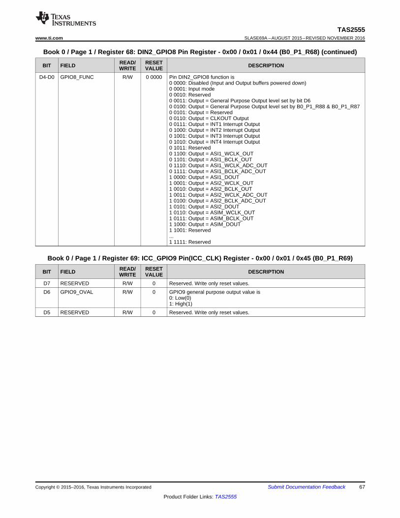
67
TAS2555www.ti.com SLASE69A –AUGUST 2015–REVISED NOVEMBER 2016
Product Folder Links: TAS2555
Submit Documentation FeedbackCopyright © 2015–2016, Texas Instruments Incorporated
Book 0 / Page 1 / Register 68: DIN2_GPIO8 Pin Register - 0x00 / 0x01 / 0x44 (B0_P1_R68) (continued)
BIT FIELD READ/WRITE
RESETVALUE DESCRIPTION
D4-D0 GPIO8_FUNC R/W 0 0000 Pin DIN2_GPIO8 function is0 0000: Disabled (Input and Output buffers powered down)0 0001: Input mode0 0010: Reserved0 0011: Output = General Purpose Output level set by bit D60 0100: Output = General Purpose Output level set by B0_P1_R88 & B0_P1_R870 0101: Output = Reserved0 0110: Output = CLKOUT Output0 0111: Output = INT1 Interrupt Output0 1000: Output = INT2 Interrupt Output0 1001: Output = INT3 Interrupt Output0 1010: Output = INT4 Interrupt Output0 1011: Reserved0 1100: Output = ASI1_WCLK_OUT0 1101: Output = ASI1_BCLK_OUT0 1110: Output = ASI1_WCLK_ADC_OUT0 1111: Output = ASI1_BCLK_ADC_OUT1 0000: Output = ASI1_DOUT1 0001: Output = ASI2_WCLK_OUT1 0010: Output = ASI2_BCLK_OUT1 0011: Output = ASI2_WCLK_ADC_OUT1 0100: Output = ASI2_BCLK_ADC_OUT1 0101: Output = ASI2_DOUT1 0110: Output = ASIM_WCLK_OUT1 0111: Output = ASIM_BCLK_OUT1 1000: Output = ASIM_DOUT1 1001: Reserved...1 1111: Reserved
Book 0 / Page 1 / Register 69: ICC_GPIO9 Pin(ICC_CLK) Register - 0x00 / 0x01 / 0x45 (B0_P1_R69)
BIT FIELD READ/WRITE
RESETVALUE DESCRIPTION
D7 RESERVED R/W 0 Reserved. Write only reset values.D6 GPIO9_OVAL R/W 0 GPIO9 general purpose output value is
0: Low(0)1: High(1)
D5 RESERVED R/W 0 Reserved. Write only reset values.

68
TAS2555SLASE69A –AUGUST 2015–REVISED NOVEMBER 2016 www.ti.com
Product Folder Links: TAS2555
Submit Documentation Feedback Copyright © 2015–2016, Texas Instruments Incorporated
Book 0 / Page 1 / Register 69: ICC_GPIO9 Pin(ICC_CLK) Register - 0x00 / 0x01 / 0x45(B0_P1_R69) (continued)
BIT FIELD READ/WRITE
RESETVALUE DESCRIPTION
D4-D0 GPIO9_FUNC R/W 0 0000 Pin ICC_GPIO9 function is0 0000: Disabled (Input and Output buffers powered down)0 0001: Input mode0 0010: Reserved0 0011: Output = General Purpose Output level set by bit D60 0100: Output = General Purpose Output level set by B0_P1_R88 & B0_P1_R870 0101: Output = Reserved0 0110: Output = CLKOUT Output0 0111: Output = INT1 Interrupt Output0 1000: Output = INT2 Interrupt Output0 1001: Output = INT3 Interrupt Output0 1010: Output = INT4 Interrupt Output0 1011: Reserved0 1100: Output = ASI1_WCLK_OUT0 1101: Output = ASI1_BCLK_OUT0 1110: Output = ASI1_WCLK_ADC_OUT0 1111: Output = ASI1_BCLK_ADC_OUT1 0000: Output = ASI1_DOUT1 0001: Output = ASI2_WCLK_OUT1 0010: Output = ASI2_BCLK_OUT1 0011: Output = ASI2_WCLK_ADC_OUT1 0100: Output = ASI2_BCLK_ADC_OUT1 0101: Output = ASI2_DOUT1 0110: Output = ASIM_WCLK_OUT1 0111: Output = ASIM_BCLK_OUT1 1000: Output = ASIM_DOUT1 1001: Reserved...1 1111: Reserved
Book 0 / Page 1 / Register 70: ICC_GPIO10 Pin Register - 0x00 / 0x01 / 0x46 (B0_P1_R70)
BIT FIELD READ/WRITE
RESETVALUE DESCRIPTION
D7 RESERVED R/W 0 Reserved. Write only reset values.D6 GPIO10_OUT_VAL R/W 0 GPIO10 General Purpose Output Value
0: Low(0)1: High(1)
D5 RESERVED R/W 0 Reserved. Write only reset values.
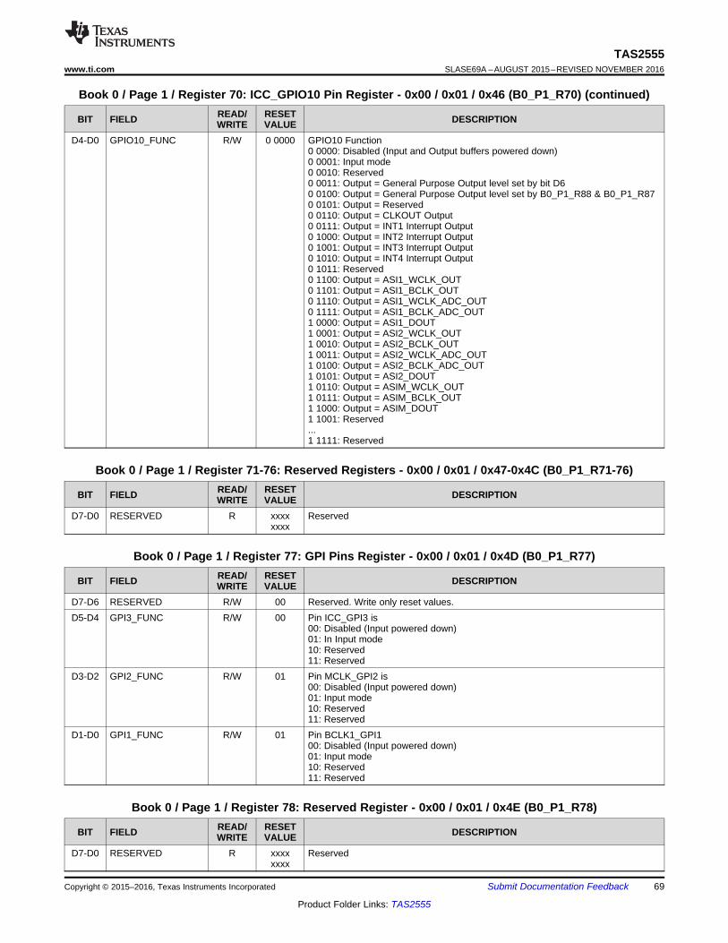
69
TAS2555www.ti.com SLASE69A –AUGUST 2015–REVISED NOVEMBER 2016
Product Folder Links: TAS2555
Submit Documentation FeedbackCopyright © 2015–2016, Texas Instruments Incorporated
Book 0 / Page 1 / Register 70: ICC_GPIO10 Pin Register - 0x00 / 0x01 / 0x46 (B0_P1_R70) (continued)
BIT FIELD READ/WRITE
RESETVALUE DESCRIPTION
D4-D0 GPIO10_FUNC R/W 0 0000 GPIO10 Function0 0000: Disabled (Input and Output buffers powered down)0 0001: Input mode0 0010: Reserved0 0011: Output = General Purpose Output level set by bit D60 0100: Output = General Purpose Output level set by B0_P1_R88 & B0_P1_R870 0101: Output = Reserved0 0110: Output = CLKOUT Output0 0111: Output = INT1 Interrupt Output0 1000: Output = INT2 Interrupt Output0 1001: Output = INT3 Interrupt Output0 1010: Output = INT4 Interrupt Output0 1011: Reserved0 1100: Output = ASI1_WCLK_OUT0 1101: Output = ASI1_BCLK_OUT0 1110: Output = ASI1_WCLK_ADC_OUT0 1111: Output = ASI1_BCLK_ADC_OUT1 0000: Output = ASI1_DOUT1 0001: Output = ASI2_WCLK_OUT1 0010: Output = ASI2_BCLK_OUT1 0011: Output = ASI2_WCLK_ADC_OUT1 0100: Output = ASI2_BCLK_ADC_OUT1 0101: Output = ASI2_DOUT1 0110: Output = ASIM_WCLK_OUT1 0111: Output = ASIM_BCLK_OUT1 1000: Output = ASIM_DOUT1 1001: Reserved...1 1111: Reserved
Book 0 / Page 1 / Register 71-76: Reserved Registers - 0x00 / 0x01 / 0x47-0x4C (B0_P1_R71-76)
BIT FIELD READ/WRITE
RESETVALUE DESCRIPTION
D7-D0 RESERVED R xxxxxxxx
Reserved
Book 0 / Page 1 / Register 77: GPI Pins Register - 0x00 / 0x01 / 0x4D (B0_P1_R77)
BIT FIELD READ/WRITE
RESETVALUE DESCRIPTION
D7-D6 RESERVED R/W 00 Reserved. Write only reset values.D5-D4 GPI3_FUNC R/W 00 Pin ICC_GPI3 is
00: Disabled (Input powered down)01: In Input mode10: Reserved11: Reserved
D3-D2 GPI2_FUNC R/W 01 Pin MCLK_GPI2 is00: Disabled (Input powered down)01: Input mode10: Reserved11: Reserved
D1-D0 GPI1_FUNC R/W 01 Pin BCLK1_GPI100: Disabled (Input powered down)01: Input mode10: Reserved11: Reserved
Book 0 / Page 1 / Register 78: Reserved Register - 0x00 / 0x01 / 0x4E (B0_P1_R78)
BIT FIELD READ/WRITE
RESETVALUE DESCRIPTION
D7-D0 RESERVED R xxxxxxxx
Reserved

70
TAS2555SLASE69A –AUGUST 2015–REVISED NOVEMBER 2016 www.ti.com
Product Folder Links: TAS2555
Submit Documentation Feedback Copyright © 2015–2016, Texas Instruments Incorporated
Book 0 / Page 1 / Register 79: GPIO HIZ CTRL1 Register - 0x00 / 0x01 / 0x4F (B0_P1_R79)
BIT FIELD READ/WRITE
RESETVALUE DESCRIPTION
D7-D5 RESERVED R/W 000 Reserved. Write only reset values.D4 GPIO2_HIZ R/W 0 GPIO2 output
000: Drives both LO/HI001: Drives both LO/HI with buskeeper(weak pull-up/down). For use with outputsthat my be tri-stated such as TDM
D3-D1 RESERVED R/W 000 Reserved. Write only reset values.D0 GPIO1_HIZ R/W 0 GPIO1 output
000: Drives both LO/HI001: Drives both LO/HI with buskeeper(weak pull-up/down). For use with outputsthat my be tri-stated such as TDM
Book 0 / Page 1 / Register 80: GPIO HIZ CTRL2 Register - 0x00 / 0x01 / 0x50 (B0_P1_R80)
BIT FIELD READ/WRITE
RESETVALUE DESCRIPTION
D7-D5 RESERVED R/W 000 Reserved. Write only reset values.D4 GPIO4_HIZ R/W 0 GPIO4 output
000: Drives both LO/HI.001: Drives both LO/HI with buskeeper(weak pull-up/down). For use with outputsthat my be tri-stated such as TDM
D3-D1 RESERVED R/W 000 Reserved. Write only reset values.D0 GPIO3_HIZ R/W 0 GPIO3 utput
000: Drives both LO/HI001: Drives both LO/HI with buskeeper(weak pull-up/down). For use with outputsthat my be tri-stated such as TDM
Book 0 / Page 1 / Register 81: GPIO HIZ CTRL3 Register - 0x00 / 0x01 / 0x51 (B0_P1_R81)
BIT FIELD READ/WRITE
RESETVALUE DESCRIPTION
D7-D5 RESERVED R/W 000 Reserved. Write only reset values.D4 GPIO6_HIZ R/W 0 GPIO6 output
000: Drives both LO/HI001: Drives both LO/HI with buskeeper(weak pull-up/down). For use with outputsthat my be tri-stated such as TDM
D3-D1 RESERVED R/W 000 Reserved. Write only reset values.D0 GPIO5_HIZ R/W 0 GPIO5 output
000: Drives both LO/HI001: Drives both LO/HI with buskeeper(weak pull-up/down). For use with outputsthat my be tri-stated such as TDM
Book 0 / Page 1 / Register 82: GPIO HIZ CTRL4 Register - 0x00 / 0x01 / 0x52 (B0_P1_R82)
BIT FIELD READ/WRITE
RESETVALUE DESCRIPTION
D7-D5 RESERVED R/W 000 Reserved. Write only reset values.D4 GPIO8_HIZ R/W 0 GPIO8 output
000: Drives both LO/HI001: Drives both LO/HI with buskeeper(weak pull-up/down). For use with outputsthat my be tri-stated such as TDM
D3-D1 RESERVED R/W 000 Reserved. Write only reset values.D0 GPIO7_HIZ R/W 0 GPIO7 output
000: Drives both LO/HI001: Drives both LO/HI with buskeeper(weak pull-up/down). For use with outputsthat my be tri-stated such as TDM

71
TAS2555www.ti.com SLASE69A –AUGUST 2015–REVISED NOVEMBER 2016
Product Folder Links: TAS2555
Submit Documentation FeedbackCopyright © 2015–2016, Texas Instruments Incorporated
Book 0 / Page 1 / Register 83: GPIO HIZ CTRL3 Register - 0x00 / 0x01 / 0x53 (B0_P1_R83)
BIT READ/WRITE
RESETVALUE DESCRIPTION
D7-D5 RESERVED R/W 000 Reserved. Write only reset values.D4 GPIO10_HIZ R/W 0 GPIO10 output
000: Drives both LO/HI001: Drives both LO/HI with buskeeper(weak pull-up/down). For use with outputsthat my be tri-stated such as TDM
D3-D1 RESERVED R/W 000 Reserved. Write only reset values.D0 GPIO9_HIZ R/W 0 GPIO9 output
000: Drives both LO/HI001: Drives both LO/HI with buskeeper(weak pull-up/down). For use with outputsthat my be tri-stated such as TDM
Book 0 / Page 1 / Register 84-86: Reserved Registers - 0x00 / 0x01 / 0x54-0x56 (B0_P1_R84-86)
BIT FIELD READ/WRITE
RESETVALUE DESCRIPTION
D7-D0 RESERVED R xxxxxxxx
Reserved.
Book 0 / Page 1 / Register 87: GPIO Pin 1 Register - 0x00 / 0x01 / 0x57 (B0_P1_R87)
BIT FIELD READ/WRITE
RESETVALUE DESCRIPTION
D7-D1 RESERVED R/W 0000 000 Reserved. Write only reset values.D0 GPO_BO_MODE R/W 0 0: Use R88,R89 to directly drive output on respective pins
1: Use DSP port to drive outputs on respective pins
Book 0 / Page 1 / Register 88: GPIO Pin 2 Register - 0x00 / 0x01 / 0x58 (B0_P1_R88)
BIT FIELD READ/WRITE
RESETVALUE DESCRIPTION
D7 GPIO8_BOV R/W 0 GPIO8 general purpose output value is0: Low(0)1: High(1)
D6 GPIO7_BOV R/W 0 GPIO7 general purpose output value is0: Low(0)1: High(1)
D5 GPIO6_BOV R/W 0 GPIO6 general purpose output value is0: Low(0)1: High(1)
D4 GPIO5_BOV R/W 0 GPIO5 general purpose output value is0: Low(0)1: High(1)
D3 GPIO4_BOV R/W 0 GPIO4 general purpose output value is0: Low(0)1: High(1)
D2 GPIO3_BOV R/W 0 GPIO3 General Purpose Output Value0: Low(0)1: High(1)
D1 GPIO2_BOV R/W 0 GPIO2 General Purpose Output Valuet0: Low(0)1: High(1)
D0 GPIO1_BOV R/W 0 GPIO1 General Purpose Output Value0: Low(0)1: High(1)

72
TAS2555SLASE69A –AUGUST 2015–REVISED NOVEMBER 2016 www.ti.com
Product Folder Links: TAS2555
Submit Documentation Feedback Copyright © 2015–2016, Texas Instruments Incorporated
Book 0 / Page 1 / Register 89: GPIO Pin 3 Register - 0x00 / 0x01 / 0x59 (B0_P1_R89)
BIT FIELD READ/WRITE
RESETVALUE DESCRIPTION
D7-D2 RESERVED R/W 0000 00 Reserved. Write only reset values.D1 GPIO10_BOV R/W 0 GPIO10 general purpose output value is
0: Low(0)1: High(1)
D0 GPIO9_BOV R/W 0 GPIO9 general purpose output value is0: Low(0)1: High(1)
Book 0 / Page 1 / Register 90-107: Reserved Registers - 0x00 / 0x01 / 0x5A-0x6B (B0_P1_R84-86)
BIT FIELD READ/WRITE
RESETVALUE DESCRIPTION
D7-D0 RESERVED R xxxxxxxx
Reserved. Write only reset values.
Book 0 / Page 1 / Register 108: Interrupt Control 1 Register - 0x00 / 0x01 / 0x6C (B0_P1_R108)
BIT FIELD READ/WRITE
RESETVALUE DESCRIPTION
D7 RESERVED R/W 0 Reserved. Write only reset values.D6-D4 INT_OVER_I R/W 000 Speaker over-current flag is
000: not used in the generation of pin interrupt001: used in the generation of INT1 interrupt010: used in the generation of INT2 interrupt011: used in the generation of INT3 interrupt100: used in the generation of INT4 interrupt101-111: Reserved
D3 RESERVED R/W 0 Reserved. Write only reset values.D2-D0 INT_OVER_V R/W 000 Speaker over-voltage flag is
000: not used in the generation of pin interrupt001: used in the generation of INT1 interrupt010: used in the generation of INT2 interrupt011: used in the generation of INT3 interrupt100: used in the generation of INT4 interrupt101-111: Reserved
Book 0 / Page 1 / Register 109: Interrupt Control 2 Register - 0x00 / 0x01 / 0x6D (B0_P1_R109)
BIT FIELD READ/WRITE
RESETVALUE DESCRIPTION
D7 RESERVED R/W 0 Reserved. Write only reset values.D6-D4 INT_CLK_ERR1 R/W 000 Clock error detect 1 flag is
000: not used in the generation of pin Interrupt001: used in the generation of INT1 Interrupt010: used in the generation of INT2 Interrupt011: used in the generation of INT3 Interrupt100: used in the generation of INT4 Interrupt101-111: Reserved
D3 RESERVED R/W 0 Reserved. Write only reset values.D2-D0 INT_OVER_TEMP R/W 0 Over-temperature flag is
000: not used in the generation of pin Interrupt001: used in the generation of INT1 interrupt010: used in the generation of INT2 interrupt011: used in the generation of INT3 interrupt100: used in the generation of INT4 interrupt101-111: Reserved

73
TAS2555www.ti.com SLASE69A –AUGUST 2015–REVISED NOVEMBER 2016
Product Folder Links: TAS2555
Submit Documentation FeedbackCopyright © 2015–2016, Texas Instruments Incorporated
Book 0 / Page 1 / Register 110: Interrupt Control 3 Register - 0x00 / 0x01 / 0x6E (B0_P1_R110)
BIT FIELD READ/WRITE
RESETVALUE DESCRIPTION
D7 RESERVED R/W 0 Reserved. Write only reset values.D6-D4 INT_BROWNOUT R/W 000 Brownout flag is
000: not used in the generation of pin Interrupt001: used in the generation of INT1 Interrupt010: used in the generation of INT2 Interrupt011: used in the generation of INT3 Interrupt100: used in the generation of INT4 Interrupt101-111: Reserved
D3 RESERVED R/W 0 Reserved. Write only reset values.D2-D0 INT_CLK_ERR2 R/W 000 Clock error detect 2 flag is
000: not used in the generation of pin Interrupt001: used in the generation of INT1 Interrupt010: used in the generation of INT2 Interrupt011: used in the generation of INT3 Interrupt100: is used in the generation of INT4 Interrupt101-111: Reserved
Book 0 / Page 1 / Register 111: Interrupt Control 4 Register - 0x00 / 0x01 / 0x6F (B0_P1_R111)
BIT FIELD READ/WRITE
RESETVALUE DESCRIPTION
D7 RESERVED R/W 0 Reserved. Write only reset values.D6-D4 INT_SAR_DONE R/W 000 SAR complete flag is
000: not used in the generation of pin Interrupt001: used in the generation of INT1 Interrupt010: used in the generation of INT2 Interrupt011: used in the generation of INT3 Interrupt100: used in the generation of INT4 Interrupt101-111: Reserved
D3-D0 R xxxx Reserved. Write only reset values.
Book 0 / Page 1 / Register 112: Interrupt Control 5 Register - 0x00 / 0x01 / 0x70 (B0_P1_R112)
BIT FIELD READ/WRITE
RESETVALUE DESCRIPTION
D7 RESERVED R/W 0 Reserved. Write only reset values.D6-D4 INT_DSP1 R/W 000 DSP output interrupt 1 flag is
000: not used in the generation of pin Interrupt001: used in the generation of INT1 Interrupt010: used in the generation of INT2 Interrupt011: used in the generation of INT3 Interrupt100: used in the generation of INT4 Interrupt101-111: Reserved
D3 RESERVED R/W 0 Reserved. Write only reset values.D2-D0 INT_DSP2 R/W 000 DSP output interrupt 2 flag is
000: not used in the generation of pin Interrupt001: used in the generation of INT1 Interrupt010: used in the generation of INT2 Interrupt011: used in the generation of INT3 Interrupt100: used in the generation of INT4 Interrupt101-111: Reserved
Book 0 / Page 1 / Register 113: Interrupt Control 6 Register - 0x00 / 0x01 / 0x71 (B0_P1_R113)
BIT FIELD READ/WRITE
RESETVALUE DESCRIPTION
D7 RESERVED R/W 0 Reserved. Write only reset values.

74
TAS2555SLASE69A –AUGUST 2015–REVISED NOVEMBER 2016 www.ti.com
Product Folder Links: TAS2555
Submit Documentation Feedback Copyright © 2015–2016, Texas Instruments Incorporated
Book 0 / Page 1 / Register 113: Interrupt Control 6 Register - 0x00 / 0x01 / 0x71 (B0_P1_R113) (continued)
BIT FIELD READ/WRITE
RESETVALUE DESCRIPTION
D6-D4 INT_DSP3 R/W 000 DSP output interrupt 3 flag is000: not used in the generation of pin Interrupt001: used in the generation of INT1 Interrupt010: used in the generation of INT2 Interrupt011: used in the generation of INT3 Interrupt100: used in the generation of INT4 Interrupt101-111: Reserved
D3 RESERVED R/W 0 Reserved. Write only reset values.D2-D0 INT_DSP4 R/W 000 DSP output interrupt 4 flag is
000: not used in the generation of pin Interrupt001: used in the generation of INT1 Interrupt010: used in the generation of INT2 Interrupt011: used in the generation of INT3 Interrupt100: used in the generation of INT4 Interrupt101-111: Reserved
Book 0 / Page 1 / Register 114-127: Reserved Register - 0x00 / 0x01 / 0x72-0x7F (B0_P1_R127)
BIT FIELD READ/WRITE
RESETVALUE DESCRIPTION
D7-D0 RESERVED R xxxxxxxx
Reserved
13.4 Book 0 Page 2
Book 0 / Page 2 / Register 0: Page Select Register - 0x00 / 0x02 / 0x00 (B0_P0_R0)
BIT FIELD READ/WRITE
RESETVALUE DESCRIPTION
D7-D0 PAGE R/W 00000000
Page Select Register0-255: Selects the Register Page for next read or write command.Refer Table for details.
Book 0 / Page 2 / Register 1-5: Reserved Register - 0x00 / 0x02 / 0x01-0x05 (B0_P1_R1-5)
BIT FIELD READ/WRITE
RESETVALUE DESCRIPTION
D7-D0 RESERVED R xxxxxxxx
Reserved
Book 0 / Page 2 / Register 6: Ramp Generator Frequency Register - 0x00 / 0x02 / 0x06 (B0_P2_R6)
BIT FIELD READ/WRITE
RESETVALUE DESCRIPTION
D7-D5 RESERVED R/W 000 Reserved. Write only reset values.D4 RAMP_FREQ R/W 0 Ramp Generator Frequency
00: 384kHz ramp_sel_res_freq = 0), Use this for Fs of 48ksps and its multiples01: 352.8kHz, Use this for Fs of 44.1ksps and its multiples
D3-D0 RESERVED R/W 0000 Reserved. Write only reset values.
Book 0 / Page 2 / Register 7-23: Reserved Register - 0x00 / 0x02 / 0x07-0x17 (B0_P1_R7-23)
BIT FIELD READ/WRITE
RESETVALUE DESCRIPTION
D7-D0 RESERVED R xxxxxxxx
Reserved

75
TAS2555www.ti.com SLASE69A –AUGUST 2015–REVISED NOVEMBER 2016
Product Folder Links: TAS2555
Submit Documentation FeedbackCopyright © 2015–2016, Texas Instruments Incorporated
Book 0 / Page 2 / Register 24: Inrush Optimization 1 Register - 0x00 / 0x02 / 0x18 (B0_P2_R24)
BIT FIELD READ/WRITE
RESETVALUE DESCRIPTION
D7-D6 RESERVED R/W 00 Reserved. Write only reset values.D5-D3 INRUSH1 R/W 101 Inrush Current Optimization 1
000: Class-H operation inrush current optimization for boost101 Not RecommendedOther: Reserved
D2-D0 INRUSH2 R/W 101 Inrush Current Optimization 2000: Class-H operation inrush current optimization for boost101 Not RecommendedOther: Reserved
Book 0 / Page 2 / Register 25: Inrush Optimization 2 Register - 0x00 / 0x02 / 0x19 (B0_P2_R25)
BIT FIELD READ/WRITE
RESETVALUE DESCRIPTION
D7-D6 RESERVED R/W 00 Reserved. Write only reset values.D5-D3 INRUSH3 R/W 101 Inrush Current Optimization 3
000: Class-H operation inrush current optimization for boost101 Not RecommendedOther: Reserved
D2-D0 INRUSH4 R/W 101 Inrush Current Optimization 4000: Class-H operation inrush current optimization for boost101 Not RecommendedOther: Reserved
Book 0 / Page 2 / Register 26: Inrush Optimization 3 Register - 0x00 / 0x02 / 0x1A (B0_P2_R25)
BIT FIELD READ/WRITE
RESETVALUE DESCRIPTION
D7-D6 RESERVED R/W 00 Reserved. Write only reset values.D5-D3 INRUSH5 R/W 101 Inrush Current Optimization 5
000: Class-H operation inrush current optimization for boost101 Not RecommendedOther: Reserved
D2-D0 INRUSH6 R/W 101 Inrush Current Optimization 6000: Class-H operation inrush current optimization for boost101 Not RecommendedOther: Reserved
Book 0 / Page 2 / Register 27: Inrush Optimization 4 Register - 0x00 / 0x02 / 0x1B (B0_P2_R25)
BIT FIELD READ/WRITE
RESETVALUE DESCRIPTION
D7-D6 RESERVED R/W 00 Reserved. Write only reset values.D5-D3 INRUSH7 R/W 101 Inrush Current Optimization 7
000: Class-H operation inrush current optimization for boost101 Not RecommendedOther: Reserved
D2-D0 INRUSH8 R/W 101 Inrush Current Optimization 8000: Class-H operation inrush current optimization for boost101 Not RecommendedOther: Reserved
Book 0 / Page 2 / Register 28-127: Reserved Register - 0x00 / 0x02 / 0x1C-0x7F (B0_P1_R28-127)
BIT FIELD READ/WRITE
RESETVALUE DESCRIPTION
D7-D0 RESERVED R xxxxxxxx
Reserved

76
TAS2555SLASE69A –AUGUST 2015–REVISED NOVEMBER 2016 www.ti.com
Product Folder Links: TAS2555
Submit Documentation Feedback Copyright © 2015–2016, Texas Instruments Incorporated
13.5 Book 100 Page 0
Book 100 / Page 0 / Register 0: Page Select Register - 0x64 / 0x00 / 0x00 (B100_P0_R0)
BIT FIELD READ/WRITE
RESETVALUE DESCRIPTION
D7-D0 PAGE R/W 00000000
Page Select Register0-255: Selects the Register Page for next read or write command.Refer Table for details.
Book 100 / Page 0 / Register 1: DAC Interpolation Register - 0x64 / 0x00 / 0x01 (B100_P0_R1)
BIT FIELD READ/WRITE
RESETVALUE DESCRIPTION
D7-D0 DAC_RATIO R/W 00001000
DAC Interpolation ratio outside DSP is0000 0000: 2560000 0001: 10000 0001: 2...1111 1110: 2541111 1111: 255
Book 100 / Page 0 / Register 2: ADC interpolation Register - 0x64 / 0x00 / 0x01 (B100_P0_R1)
BIT FIELD READ/WRITE
RESETVALUE DESCRIPTION
D7-D6 RESERVED R/W 00 Reserved. Write only reset values.D5-D0 ADC_RATIO R/W 00 0000 ADC interpolation ratio outside DSP is
00 0000: 6400 0001: 100 0001: 2...10 0101: 3710 0110: 38 (maximum ratio supported for Isense/Vsense)10 0111: 39 (supported only for PDM audio input)10 1000: 40 (supported only for PDM audio input)10 1001: 41 (supported only for PDM audio input)10 1010: 42 (supported only for PDM audio input)10 1011: 43 (supported only for PDM audio input)10 1100: 44 (supported only for PDM audio input)10 1101: 45 (supported only for PDM audio input)
Book 100 / Page 0 / Register 3-6: Reserved Register - 0x64 / 0x00 / 0x03-0x06 (B100_P0_R3-6)
BIT FIELD READ/WRITE
RESETVALUE DESCRIPTION
D7-D0 RESERVED R xxxxxxxx
Reserved.
Book 100 / Page 0 / Register 7: DSP Mute Register - 0x64 / 0x00 / 0x07 (B100_P0_R7)
BIT FIELD READ/WRITE
RESETVALUE DESCRIPTION
D7-D4 RESERVED R/W 0000 Reserved. Write only reset values.D3 PDM_MUTE R/W 1 PDM soft mute is
0: un-mute1: mute
D2 VSNS_MUTE R/W 1 Vsense soft mute is0: un-mute1: mute
D1 ISNS_MUTE R/W 1 Isense soft mute is0: un-mute1: mute
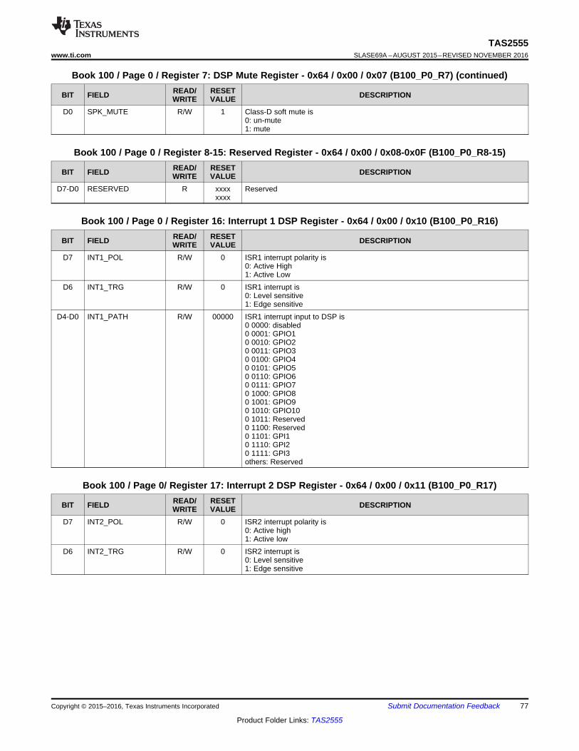
77
TAS2555www.ti.com SLASE69A –AUGUST 2015–REVISED NOVEMBER 2016
Product Folder Links: TAS2555
Submit Documentation FeedbackCopyright © 2015–2016, Texas Instruments Incorporated
Book 100 / Page 0 / Register 7: DSP Mute Register - 0x64 / 0x00 / 0x07 (B100_P0_R7) (continued)
BIT FIELD READ/WRITE
RESETVALUE DESCRIPTION
D0 SPK_MUTE R/W 1 Class-D soft mute is0: un-mute1: mute
Book 100 / Page 0 / Register 8-15: Reserved Register - 0x64 / 0x00 / 0x08-0x0F (B100_P0_R8-15)
BIT FIELD READ/WRITE
RESETVALUE DESCRIPTION
D7-D0 RESERVED R xxxxxxxx
Reserved
Book 100 / Page 0 / Register 16: Interrupt 1 DSP Register - 0x64 / 0x00 / 0x10 (B100_P0_R16)
BIT FIELD READ/WRITE
RESETVALUE DESCRIPTION
D7 INT1_POL R/W 0 ISR1 interrupt polarity is0: Active High1: Active Low
D6 INT1_TRG R/W 0 ISR1 interrupt is0: Level sensitive1: Edge sensitive
D4-D0 INT1_PATH R/W 00000 ISR1 interrupt input to DSP is0 0000: disabled0 0001: GPIO10 0010: GPIO20 0011: GPIO30 0100: GPIO40 0101: GPIO50 0110: GPIO60 0111: GPIO70 1000: GPIO80 1001: GPIO90 1010: GPIO100 1011: Reserved0 1100: Reserved0 1101: GPI10 1110: GPI20 1111: GPI3others: Reserved
Book 100 / Page 0/ Register 17: Interrupt 2 DSP Register - 0x64 / 0x00 / 0x11 (B100_P0_R17)
BIT FIELD READ/WRITE
RESETVALUE DESCRIPTION
D7 INT2_POL R/W 0 ISR2 interrupt polarity is0: Active high1: Active low
D6 INT2_TRG R/W 0 ISR2 interrupt is0: Level sensitive1: Edge sensitive

78
TAS2555SLASE69A –AUGUST 2015–REVISED NOVEMBER 2016 www.ti.com
Product Folder Links: TAS2555
Submit Documentation Feedback Copyright © 2015–2016, Texas Instruments Incorporated
Book 100 / Page 0/ Register 17: Interrupt 2 DSP Register - 0x64 / 0x00 / 0x11 (B100_P0_R17) (continued)
BIT FIELD READ/WRITE
RESETVALUE DESCRIPTION
D4-D0 INT2_PATH R/W 00000 ISR2 interrupt input to DSP is0 0000: disabled0 0001: GPIO10 0010: GPIO20 0011: GPIO30 0100: GPIO40 0101: GPIO50 0110: GPIO60 0111: GPIO70 1000: GPIO80 1001: GPIO90 1010: GPIO100 1011: Reserved0 1100: Reserved0 1101: GPI10 1110: GPI20 1111: GPI3others: Reserved
Book 100 / Page 0 / Register 18: Condition 1 DSP Register - 0x64 / 0x00 / 0x12 (B100_P0_R18)
BIT FIELD READ/WRITE
RESETVALUE DESCRIPTION
D7 COND1_POL R/W 0 COND1 interrupt polarity is0: Active high1: Active low
D6 COND1_TRG R/W 0 COND1 interrupt is0: Level sensitive1: Edge sensitive
D4-D0 COND1_PATH R/W 00000 COND1 interrupt input to DSP is0 0000: disabled0 0001: GPIO10 0010: GPIO20 0011: GPIO30 0100: GPIO40 0101: GPIO50 0110: GPIO60 0111: GPIO70 1000: GPIO80 1001: GPIO90 1010: GPIO100 1011: Reserved0 1100: Reserved0 1101: GPI10 1110: GPI20 1111: GPI3others: Reserved
Book 100/ Page 0 / Register 19: Condition 2 DSP Register - 0x64 / 0x00 / 0x13 (B100_P0_R19)
BIT FIELD READ/WRITE
RESETVALUE DESCRIPTION
D7 COND2_POL R/W 0 COND2 interrupt polarity is0: Active High1: Active Low
D6 COND2_TRG R/W 0 COND2 interrupt is0: Level Sensitive1: Edge Sensitive
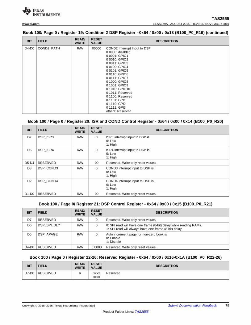
79
TAS2555www.ti.com SLASE69A –AUGUST 2015–REVISED NOVEMBER 2016
Product Folder Links: TAS2555
Submit Documentation FeedbackCopyright © 2015–2016, Texas Instruments Incorporated
Book 100/ Page 0 / Register 19: Condition 2 DSP Register - 0x64 / 0x00 / 0x13 (B100_P0_R19) (continued)
BIT FIELD READ/WRITE
RESETVALUE DESCRIPTION
D4-D0 COND2_PATH R/W 00000 COND2 Interrupt Input to DSP0 0000: disabled0 0001: GPIO10 0010: GPIO20 0011: GPIO30 0100: GPIO40 0101: GPIO50 0110: GPIO60 0111: GPIO70 1000: GPIO80 1001: GPIO90 1010: GPIO100 1011: Reserved0 1100: Reserved0 1101: GPI10 1110: GPI20 1111: GPI3others: Reserved
Book 100 / Page 0 / Register 20: ISR and COND Control Register - 0x64 / 0x00 / 0x14 (B100_P0_R20)
BIT FIELD READ/WRITE
RESETVALUE DESCRIPTION
D7 DSP_ISR3 R/W 0 ISR3 interrupt input to DSP is0: Low1: High
D6 DSP_ISR4 R/W 0 ISR4 interrupt input to DSP is0: Low1: High
D5-D4 RESERVED R/W 00 Reserved. Write only reset values.D3 DSP_COND3 R/W 0 COND3 interrupt input to DSP is
0: Low1: High
D2 DSP_COND4 COND4 interrupt input to DSP is0: Low1: High
D1-D0 RESERVED R/W 00 Reserved. Write only reset values.
Book 100 / Page 0/ Register 21: DSP Control Register - 0x64 / 0x00 / 0x15 (B100_P0_R21)
BIT FIELD READ/WRITE
RESETVALUE DESCRIPTION
D7 RESERVED R/W 0 Reserved. Write only reset values.D6 DSP_SPI_DLY R/W 0 0: SPI read will have one frame (8-bit) delay while reading RAMs.
1: SPI read will always have one frame (8-bit) delayD5 DSP_APAGE R/W 0 Auto increment page for non-zero book is
0: Enable1: Disable
D4-D0 RESERVED R/W 0 0000 Reserved. Write only reset values.
Book 100 / Page 0 / Register 22-26: Reserved Register - 0x64 / 0x00 / 0x16-0x1A (B100_P0_R22-26)
BIT FIELD READ/WRITE
RESETVALUE DESCRIPTION
D7-D0 RESERVED R xxxxxxxx
Reserved

80
TAS2555SLASE69A –AUGUST 2015–REVISED NOVEMBER 2016 www.ti.com
Product Folder Links: TAS2555
Submit Documentation Feedback Copyright © 2015–2016, Texas Instruments Incorporated
Book 100 / Page 0 / Register 27:PLL CLKIN Divider Register - 0x64 / 0x00 / 0x1B (B100_P0_R27)
BIT FIELD READ/WRITE
RESETVALUE DESCRIPTION
D7-D6 RESERVED R/W 00 Reserved. Write only reset values.D5-D0 PLL_PDIV R/W 00 0001 PLL_CLKIN divider (generates input clock for PLL P-divider) is
00 0000: 6400 0001: 100 0001: 2...11 1110: 6211 1111: 63
Book 100 / Page 0 / Register 28:PLL J-VAL Divider Register - 0x64 / 0x00 / 0x1C (B100_P0_R28)
BIT FIELD READ/WRITE
RESETVALUE DESCRIPTION
D7 PLL_LOW R/W 0 PLL low input frequency is0: should be set when PLL CLKIN divider output is greater than 1MHz1: should be set when PLL CLKIN divider output is less than 1MHz
D6-D0 PLL_JDIV R/W 00 0100 PLL J multiplier is00 0000: Reserved00 0001: 100 0010: 2...11 1110: 6211 1111: 63
Book 100 / Page 0 / Register 29:PLL D-VAL Divider 2 Register - 0x64 / 0x00 / 0x1D (B100_P0_R29)
BIT FIELD READ/WRITE
RESETVALUE DESCRIPTION
D7 RESERVED R/W 0 Reserved. Write only reset values.D6-D0 PLL_DVAL2 R/W 000 0000 PLL D Factional Multiplier D(13:8)
Book 100 / Page 0 / Register 30:PLL D-VAL Divider 1 Register - 0x64 / 0x00 / 0x1E (B100_P0_R30)
BIT FIELD READ/WRITE
RESETVALUE DESCRIPTION
D7-D0 PLL_DVAL1 R/W 00000000
PLL D Factional Multiplier D(7:0)
Book 100 / Page 0 / Register 31:DSP Clock Register - 0x64 / 0x00 / 0x1F (B100_P0_R31)
BIT FIELD READ/WRITE
RESETVALUE DESCRIPTION
D7-D6 RESERVED R/W 00 Reserved. Write only reset values.D5 DSP_CLK R/W 0 DSP clock is generated from
0: output of N_VAL divider in B100_P0_R321: directly from PLL Clock
D4-D3 MDAC_CLK R/W 00 MDAC and MADC is clock divider input is00: NDIV_CLK (N-divider output)01: MCLK_GPI2. This can be used only if MCLK is multiple of 8*64*Fs or4*64*Fs(with 48-52% duty-cycle)10: ICC_GPIO9. This can be used only if MCLK is multiple of 8*64*Fs or4*64*Fs(with 48-52% duty-cycle)11: Reserved
D2-D1 BOOST_CLK R/W 00 Boost and Charge-pump divider input is00: NDIV_CLK (N-divider output)01: MCLK_GPI2.10: ICC_GPIO9.11: Reserved
D0 RESERVED R/W 0 Reserved. Write only reset values.
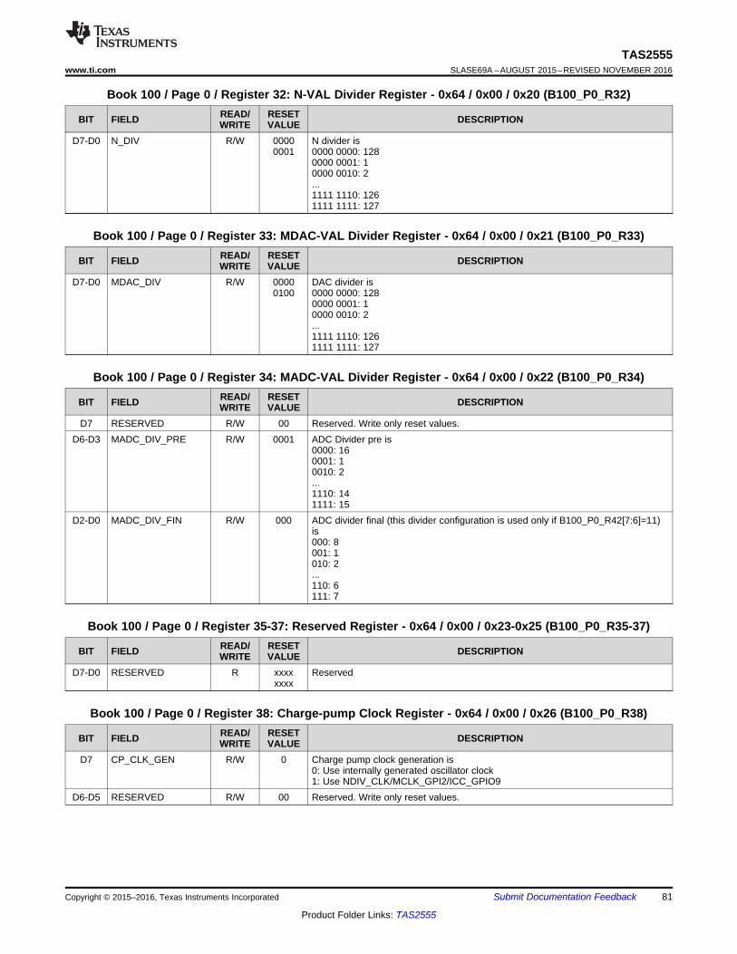
81
TAS2555www.ti.com SLASE69A –AUGUST 2015–REVISED NOVEMBER 2016
Product Folder Links: TAS2555
Submit Documentation FeedbackCopyright © 2015–2016, Texas Instruments Incorporated
Book 100 / Page 0 / Register 32: N-VAL Divider Register - 0x64 / 0x00 / 0x20 (B100_P0_R32)
BIT FIELD READ/WRITE
RESETVALUE DESCRIPTION
D7-D0 N_DIV R/W 00000001
N divider is0000 0000: 1280000 0001: 10000 0010: 2...1111 1110: 1261111 1111: 127
Book 100 / Page 0 / Register 33: MDAC-VAL Divider Register - 0x64 / 0x00 / 0x21 (B100_P0_R33)
BIT FIELD READ/WRITE
RESETVALUE DESCRIPTION
D7-D0 MDAC_DIV R/W 00000100
DAC divider is0000 0000: 1280000 0001: 10000 0010: 2...1111 1110: 1261111 1111: 127
Book 100 / Page 0 / Register 34: MADC-VAL Divider Register - 0x64 / 0x00 / 0x22 (B100_P0_R34)
BIT FIELD READ/WRITE
RESETVALUE DESCRIPTION
D7 RESERVED R/W 00 Reserved. Write only reset values.D6-D3 MADC_DIV_PRE R/W 0001 ADC Divider pre is
0000: 160001: 10010: 2...1110: 141111: 15
D2-D0 MADC_DIV_FIN R/W 000 ADC divider final (this divider configuration is used only if B100_P0_R42[7:6]=11)is000: 8001: 1010: 2...110: 6111: 7
Book 100 / Page 0 / Register 35-37: Reserved Register - 0x64 / 0x00 / 0x23-0x25 (B100_P0_R35-37)
BIT FIELD READ/WRITE
RESETVALUE DESCRIPTION
D7-D0 RESERVED R xxxxxxxx
Reserved
Book 100 / Page 0 / Register 38: Charge-pump Clock Register - 0x64 / 0x00 / 0x26 (B100_P0_R38)
BIT FIELD READ/WRITE
RESETVALUE DESCRIPTION
D7 CP_CLK_GEN R/W 0 Charge pump clock generation is0: Use internally generated oscillator clock1: Use NDIV_CLK/MCLK_GPI2/ICC_GPIO9
D6-D5 RESERVED R/W 00 Reserved. Write only reset values.
82
TAS2555SLASE69A –AUGUST 2015–REVISED NOVEMBER 2016 www.ti.com
Product Folder Links: TAS2555
Submit Documentation Feedback Copyright © 2015–2016, Texas Instruments Incorporated
Book 100 / Page 0 / Register 38: Charge-pump Clock Register - 0x64 / 0x00 / 0x26(B100_P0_R38) (continued)
BIT FIELD READ/WRITE
RESETVALUE DESCRIPTION
D4-D0 CP_CLK_DIV R/W 0010 Charge pump clock divider factor is0 0000: 320 0001: 10 0010: 2...1 1110: 301 1111: 31
Book 100 / Page 0 / Register 39: Boost Clock Register - 0x64 / 0x00 / 0x27 (B100_P0_R39)
BIT FIELD READ/WRITE
RESETVALUE DESCRIPTION
D7 RMP_CLK_GEN R/W 0 Boost clock generation uses0: internally generated oscillator clock1: NDIV_CLK/MCLK_GPI2/ICC_GPIO9
D6-D3 BST_DIV_PRE R/W 0010 Boost clock pre divider factor is0000: 160001: 10010: 2...1110: 141111: 15
D2-D0 BST_DIV_FIN R/W 011 ADC divider final (this divider configuration is used only if B100_P0_R42[7:6]=11)is000: 8001: 1010: 2...110: 6111: 7
Book 100 / Page 0 / Register 40: Ramp Clock 1 Register - 0x64 / 0x00 / 0x28 (B100_P0_R40)
BIT FIELD READ/WRITE
RESETVALUE DESCRIPTION
D7 RMP_CLK_GEN R/W 0 Ramp clock generation is0: internally generated1: from DAC modulator clock (Refer to divider settings in B100_P0_R43-44)
D6-D0 RESERVED R/W 000 0000 Reserved. Write only reset values.
Book 100 / Page 0 / Register 41-42: Reserved Register - 0x64 / 0x00 / 0x29-0x2A (B100_P0_R41-42)
BIT FIELD READ/WRITE
RESETVALUE DESCRIPTION
D7-D0 RESERVED R xxxxxxxx
Reserved.
Book 100 / Page 0 / Register 43: Ramp Clock 2 Register - 0x64 / 0x00 / 0x2B (B100_P0_R43)
BIT FIELD READ/WRITE
RESETVALUE DESCRIPTION
D7-D3 RESERVED R/W 0000 0 Reserved. Write only reset values.D2-D0 RMP_CLK_MSB R/W 000 Ramp Clock Divider [10:8]
Book 100 / Page 0 / Register 44: Ramp Clock 3 Register - 0x64 / 0x00 / 0x2C (B100_P0_R44)
BIT FIELD READ/WRITE
RESETVALUE DESCRIPTION
D7-D0 RMP_CLK_LSB R/W 000 Ramp Clock Divider [7:0]

83
TAS2555www.ti.com SLASE69A –AUGUST 2015–REVISED NOVEMBER 2016
Product Folder Links: TAS2555
Submit Documentation FeedbackCopyright © 2015–2016, Texas Instruments Incorporated
Book 100 / Page 0/ Register 45-126: Reserved Register - 0x64 / 0x01 / 0x2D-0x7E (B100_P0_R45-126)
BIT FIELD READ/WRITE
RESETVALUE DESCRIPTION
D7-D0 RESERVED R xxxxxxxx
Reserved.
Book 100 / Page 0 / Register 127: Book Selection Register - 0x64 / 0x00 / 0x7F (B100_P0_R127)
BIT FIELD READ/WRITE
RESETVALUE DESCRIPTION
D7-D0 BOOK R/W 01100100
0-255: Selects the Register Book for next read or write command.

84
TAS2555SLASE69A –AUGUST 2015–REVISED NOVEMBER 2016 www.ti.com
Product Folder Links: TAS2555
Submit Documentation Feedback Copyright © 2015–2016, Texas Instruments Incorporated
14 Device and Documentation Support
14.1 Documentation Support
14.2 Community ResourcesThe following links connect to TI community resources. Linked contents are provided "AS IS" by the respectivecontributors. They do not constitute TI specifications and do not necessarily reflect TI's views; see TI's Terms ofUse.
TI E2E™ Online Community TI's Engineer-to-Engineer (E2E) Community. Created to foster collaborationamong engineers. At e2e.ti.com, you can ask questions, share knowledge, explore ideas and helpsolve problems with fellow engineers.
Design Support TI's Design Support Quickly find helpful E2E forums along with design support tools andcontact information for technical support.
14.3 TrademarksPurePath, E2E are trademarks of Texas Instruments.All other trademarks are the property of their respective owners.
14.4 Electrostatic Discharge CautionThese devices have limited built-in ESD protection. The leads should be shorted together or the device placed in conductive foamduring storage or handling to prevent electrostatic damage to the MOS gates.
14.5 GlossarySLYZ022 — TI Glossary.
This glossary lists and explains terms, acronyms, and definitions.
15 Mechanical, Packaging, and Orderable InformationThe following pages include mechanical, packaging, and orderable information. This information is the mostcurrent data available for the designated devices. This data is subject to change without notice and revision ofthis document. For browser-based versions of this data sheet, refer to the left-hand navigation.
15.1 Package DimensionsThe TAS2555 uses a 42-ball, 0.5-mm pitch DSBGA package. The die length (D) and width (E) correspond to thepackage mechanical drawing at the end of the datasheet.

www.ti.com
PACKAGE OUTLINE
C0.625 MAX
0.350.15
3
TYP
2.5 TYP
0.5 TYP
0.5 TYP
42X0.350.25
1.307
B3.2593.199 A
3.5053.445
(0.4215)(0.3075)
4222036/A 04/2015
DSBGA - 0.625 mm max heightYZ0042-C01DIE SIZE BALL GRID ARRAY
NOTES:
1. All linear dimensions are in millimeters. Any dimensions in parenthesis are for reference only. Dimensioning and tolerancingper ASME Y14.5M.
2. This drawing is subject to change without notice.
TAS2555YZ
BUMP A1CORNER
SEATING PLANE
BALL TYP0.05 C
A
B
C
D
1 2 3
0.015 C A B
E
54
F
G
SYMM
6
PKG
SCALE 4.000
85
TAS2555www.ti.com SLASE69A –AUGUST 2015–REVISED NOVEMBER 2016
Product Folder Links: TAS2555
Submit Documentation FeedbackCopyright © 2015–2016, Texas Instruments Incorporated
Package Dimensions (continued)

www.ti.com
EXAMPLE BOARD LAYOUT
42X ( )0.245
(0.5) TYP
(0.5) TYP
( )METAL0.245 0.05 MAX
SOLDER MASKOPENING
METAL UNDERSOLDER MASK
( )SOLDER MASKOPENING
0.2450.05 MIN
(1.307)
4222036/A 04/2015
DSBGA - 0.625 mm max heightYZ0042-C01DIE SIZE BALL GRID ARRAY
NOTES: (continued)
3. Final dimensions may vary due to manufacturing tolerance considerations and also routing constraints.For more information, see Texas Instruments literature number SNVA009 (www.ti.com/lit/snva009).
SOLDER MASK DETAILSNOT TO SCALE
SYMM
TAS2555YZ
PKG
LAND PATTERN EXAMPLESCALE:20X
A
B
C
D
1 2 3 4 5
E
F
G
6
NON-SOLDER MASKDEFINED
(PREFERRED)
SOLDER MASKDEFINED
86
TAS2555SLASE69A –AUGUST 2015–REVISED NOVEMBER 2016 www.ti.com
Product Folder Links: TAS2555
Submit Documentation Feedback Copyright © 2015–2016, Texas Instruments Incorporated
Package Dimensions (continued)
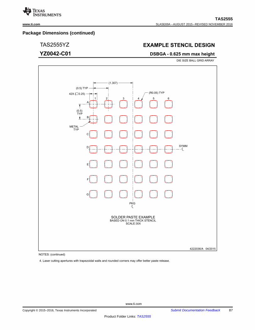
www.ti.com
EXAMPLE STENCIL DESIGN
(0.5)TYP
(0.5) TYP
42X ( 0.25) (R ) TYP0.05
METALTYP
(1.307)
4222036/A 04/2015
DSBGA - 0.625 mm max heightYZ0042-C01DIE SIZE BALL GRID ARRAY
NOTES: (continued)
4. Laser cutting apertures with trapezoidal walls and rounded corners may offer better paste release.
TAS2555YZ
PKG
SYMM
SOLDER PASTE EXAMPLEBASED ON 0.1 mm THICK STENCIL
SCALE:30X
A
B
C
D
1 2 3
E
4 5
F
G
6
87
TAS2555www.ti.com SLASE69A –AUGUST 2015–REVISED NOVEMBER 2016
Product Folder Links: TAS2555
Submit Documentation FeedbackCopyright © 2015–2016, Texas Instruments Incorporated
Package Dimensions (continued)

PACKAGE OPTION ADDENDUM
www.ti.com 15-Nov-2016
Addendum-Page 1
PACKAGING INFORMATION
Orderable Device Status(1)
Package Type PackageDrawing
Pins PackageQty
Eco Plan(2)
Lead/Ball Finish(6)
MSL Peak Temp(3)
Op Temp (°C) Device Marking(4/5)
Samples
TAS2555YZR ACTIVE DSBGA YZ 42 3000 Green (RoHS& no Sb/Br)
SNAGCU Level-1-260C-UNLIM -40 to 85 2555
TAS2555YZT ACTIVE DSBGA YZ 42 250 Green (RoHS& no Sb/Br)
SNAGCU Level-1-260C-UNLIM -40 to 85 2555
(1) The marketing status values are defined as follows:ACTIVE: Product device recommended for new designs.LIFEBUY: TI has announced that the device will be discontinued, and a lifetime-buy period is in effect.NRND: Not recommended for new designs. Device is in production to support existing customers, but TI does not recommend using this part in a new design.PREVIEW: Device has been announced but is not in production. Samples may or may not be available.OBSOLETE: TI has discontinued the production of the device.
(2) Eco Plan - The planned eco-friendly classification: Pb-Free (RoHS), Pb-Free (RoHS Exempt), or Green (RoHS & no Sb/Br) - please check http://www.ti.com/productcontent for the latest availabilityinformation and additional product content details.TBD: The Pb-Free/Green conversion plan has not been defined.Pb-Free (RoHS): TI's terms "Lead-Free" or "Pb-Free" mean semiconductor products that are compatible with the current RoHS requirements for all 6 substances, including the requirement thatlead not exceed 0.1% by weight in homogeneous materials. Where designed to be soldered at high temperatures, TI Pb-Free products are suitable for use in specified lead-free processes.Pb-Free (RoHS Exempt): This component has a RoHS exemption for either 1) lead-based flip-chip solder bumps used between the die and package, or 2) lead-based die adhesive used betweenthe die and leadframe. The component is otherwise considered Pb-Free (RoHS compatible) as defined above.Green (RoHS & no Sb/Br): TI defines "Green" to mean Pb-Free (RoHS compatible), and free of Bromine (Br) and Antimony (Sb) based flame retardants (Br or Sb do not exceed 0.1% by weightin homogeneous material)
(3) MSL, Peak Temp. - The Moisture Sensitivity Level rating according to the JEDEC industry standard classifications, and peak solder temperature.
(4) There may be additional marking, which relates to the logo, the lot trace code information, or the environmental category on the device.
(5) Multiple Device Markings will be inside parentheses. Only one Device Marking contained in parentheses and separated by a "~" will appear on a device. If a line is indented then it is a continuationof the previous line and the two combined represent the entire Device Marking for that device.
(6) Lead/Ball Finish - Orderable Devices may have multiple material finish options. Finish options are separated by a vertical ruled line. Lead/Ball Finish values may wrap to two lines if the finishvalue exceeds the maximum column width.
Important Information and Disclaimer:The information provided on this page represents TI's knowledge and belief as of the date that it is provided. TI bases its knowledge and belief on informationprovided by third parties, and makes no representation or warranty as to the accuracy of such information. Efforts are underway to better integrate information from third parties. TI has taken andcontinues to take reasonable steps to provide representative and accurate information but may not have conducted destructive testing or chemical analysis on incoming materials and chemicals.TI and TI suppliers consider certain information to be proprietary, and thus CAS numbers and other limited information may not be available for release.

PACKAGE OPTION ADDENDUM
www.ti.com 15-Nov-2016
Addendum-Page 2
In no event shall TI's liability arising out of such information exceed the total purchase price of the TI part(s) at issue in this document sold by TI to Customer on an annual basis.
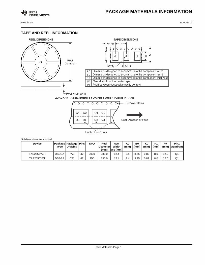
TAPE AND REEL INFORMATION
*All dimensions are nominal
Device PackageType
PackageDrawing
Pins SPQ ReelDiameter
(mm)
ReelWidth
W1 (mm)
A0(mm)
B0(mm)
K0(mm)
P1(mm)
W(mm)
Pin1Quadrant
TAS2555YZR DSBGA YZ 42 3000 330.0 12.4 3.4 3.75 0.82 8.0 12.0 Q1
TAS2555YZT DSBGA YZ 42 250 330.0 12.4 3.4 3.75 0.82 8.0 12.0 Q1
PACKAGE MATERIALS INFORMATION
www.ti.com 1-Dec-2016
Pack Materials-Page 1
*All dimensions are nominal
Device Package Type Package Drawing Pins SPQ Length (mm) Width (mm) Height (mm)
TAS2555YZR DSBGA YZ 42 3000 367.0 367.0 35.0
TAS2555YZT DSBGA YZ 42 250 367.0 367.0 35.0
PACKAGE MATERIALS INFORMATION
www.ti.com 1-Dec-2016
Pack Materials-Page 2

IMPORTANT NOTICE
Texas Instruments Incorporated (TI) reserves the right to make corrections, enhancements, improvements and other changes to itssemiconductor products and services per JESD46, latest issue, and to discontinue any product or service per JESD48, latest issue. Buyersshould obtain the latest relevant information before placing orders and should verify that such information is current and complete.TI’s published terms of sale for semiconductor products (http://www.ti.com/sc/docs/stdterms.htm) apply to the sale of packaged integratedcircuit products that TI has qualified and released to market. Additional terms may apply to the use or sale of other types of TI products andservices.Reproduction of significant portions of TI information in TI data sheets is permissible only if reproduction is without alteration and isaccompanied by all associated warranties, conditions, limitations, and notices. TI is not responsible or liable for such reproduceddocumentation. Information of third parties may be subject to additional restrictions. Resale of TI products or services with statementsdifferent from or beyond the parameters stated by TI for that product or service voids all express and any implied warranties for theassociated TI product or service and is an unfair and deceptive business practice. TI is not responsible or liable for any such statements.Buyers and others who are developing systems that incorporate TI products (collectively, “Designers”) understand and agree that Designersremain responsible for using their independent analysis, evaluation and judgment in designing their applications and that Designers havefull and exclusive responsibility to assure the safety of Designers' applications and compliance of their applications (and of all TI productsused in or for Designers’ applications) with all applicable regulations, laws and other applicable requirements. Designer represents that, withrespect to their applications, Designer has all the necessary expertise to create and implement safeguards that (1) anticipate dangerousconsequences of failures, (2) monitor failures and their consequences, and (3) lessen the likelihood of failures that might cause harm andtake appropriate actions. Designer agrees that prior to using or distributing any applications that include TI products, Designer willthoroughly test such applications and the functionality of such TI products as used in such applications.TI’s provision of technical, application or other design advice, quality characterization, reliability data or other services or information,including, but not limited to, reference designs and materials relating to evaluation modules, (collectively, “TI Resources”) are intended toassist designers who are developing applications that incorporate TI products; by downloading, accessing or using TI Resources in anyway, Designer (individually or, if Designer is acting on behalf of a company, Designer’s company) agrees to use any particular TI Resourcesolely for this purpose and subject to the terms of this Notice.TI’s provision of TI Resources does not expand or otherwise alter TI’s applicable published warranties or warranty disclaimers for TIproducts, and no additional obligations or liabilities arise from TI providing such TI Resources. TI reserves the right to make corrections,enhancements, improvements and other changes to its TI Resources. TI has not conducted any testing other than that specificallydescribed in the published documentation for a particular TI Resource.Designer is authorized to use, copy and modify any individual TI Resource only in connection with the development of applications thatinclude the TI product(s) identified in such TI Resource. NO OTHER LICENSE, EXPRESS OR IMPLIED, BY ESTOPPEL OR OTHERWISETO ANY OTHER TI INTELLECTUAL PROPERTY RIGHT, AND NO LICENSE TO ANY TECHNOLOGY OR INTELLECTUAL PROPERTYRIGHT OF TI OR ANY THIRD PARTY IS GRANTED HEREIN, including but not limited to any patent right, copyright, mask work right, orother intellectual property right relating to any combination, machine, or process in which TI products or services are used. Informationregarding or referencing third-party products or services does not constitute a license to use such products or services, or a warranty orendorsement thereof. Use of TI Resources may require a license from a third party under the patents or other intellectual property of thethird party, or a license from TI under the patents or other intellectual property of TI.TI RESOURCES ARE PROVIDED “AS IS” AND WITH ALL FAULTS. TI DISCLAIMS ALL OTHER WARRANTIES ORREPRESENTATIONS, EXPRESS OR IMPLIED, REGARDING RESOURCES OR USE THEREOF, INCLUDING BUT NOT LIMITED TOACCURACY OR COMPLETENESS, TITLE, ANY EPIDEMIC FAILURE WARRANTY AND ANY IMPLIED WARRANTIES OFMERCHANTABILITY, FITNESS FOR A PARTICULAR PURPOSE, AND NON-INFRINGEMENT OF ANY THIRD PARTY INTELLECTUALPROPERTY RIGHTS. TI SHALL NOT BE LIABLE FOR AND SHALL NOT DEFEND OR INDEMNIFY DESIGNER AGAINST ANY CLAIM,INCLUDING BUT NOT LIMITED TO ANY INFRINGEMENT CLAIM THAT RELATES TO OR IS BASED ON ANY COMBINATION OFPRODUCTS EVEN IF DESCRIBED IN TI RESOURCES OR OTHERWISE. IN NO EVENT SHALL TI BE LIABLE FOR ANY ACTUAL,DIRECT, SPECIAL, COLLATERAL, INDIRECT, PUNITIVE, INCIDENTAL, CONSEQUENTIAL OR EXEMPLARY DAMAGES INCONNECTION WITH OR ARISING OUT OF TI RESOURCES OR USE THEREOF, AND REGARDLESS OF WHETHER TI HAS BEENADVISED OF THE POSSIBILITY OF SUCH DAMAGES.Unless TI has explicitly designated an individual product as meeting the requirements of a particular industry standard (e.g., ISO/TS 16949and ISO 26262), TI is not responsible for any failure to meet such industry standard requirements.Where TI specifically promotes products as facilitating functional safety or as compliant with industry functional safety standards, suchproducts are intended to help enable customers to design and create their own applications that meet applicable functional safety standardsand requirements. Using products in an application does not by itself establish any safety features in the application. Designers mustensure compliance with safety-related requirements and standards applicable to their applications. Designer may not use any TI products inlife-critical medical equipment unless authorized officers of the parties have executed a special contract specifically governing such use.Life-critical medical equipment is medical equipment where failure of such equipment would cause serious bodily injury or death (e.g., lifesupport, pacemakers, defibrillators, heart pumps, neurostimulators, and implantables). Such equipment includes, without limitation, allmedical devices identified by the U.S. Food and Drug Administration as Class III devices and equivalent classifications outside the U.S.TI may expressly designate certain products as completing a particular qualification (e.g., Q100, Military Grade, or Enhanced Product).Designers agree that it has the necessary expertise to select the product with the appropriate qualification designation for their applicationsand that proper product selection is at Designers’ own risk. Designers are solely responsible for compliance with all legal and regulatoryrequirements in connection with such selection.Designer will fully indemnify TI and its representatives against any damages, costs, losses, and/or liabilities arising out of Designer’s non-compliance with the terms and provisions of this Notice.
Mailing Address: Texas Instruments, Post Office Box 655303, Dallas, Texas 75265Copyright © 2017, Texas Instruments Incorporated


