Embed Size (px)
Citation preview

1264IEICE TRANS. ELECTRON., VOL.E99–C, NO.11 NOVEMBER 2016
INVITED PAPER Special Section on Electronic Displays
Development of Zinc Oxide Spatial Light Modulator for High-YieldSpeckle Modulation
Naoya TATE†a), Tadashi KAWAZOE††, Shunsuke NAKASHIMA†, Wataru NOMURA†, Nonmembers,and Motoichi OHTSU††, Member
SUMMARY In order to realize high-yield speckle modulation, we de-veloped a novel spatial light modulator using zinc oxide single crystaldoped with nitrogen ions. The distribution of dopants was optimized toinduce characteristic optical functions by applying an annealing methoddeveloped by us. The device is driven by a current in the in-plane direc-tion, which induces magnetic fields. These fields strongly interact with thedoped material, and the spatial distribution of the refractive index is corre-spondingly modulated via external control. Using this device, we experi-mentally demonstrated speckle modulation, and we discuss the quantitativesuperiority of our approach.key words: nanophotonics, spatial light modulator, laser speckle, specklemodulation, oxide semiconductor
1. Introduction
Laser projection systems are advanced display systems withhigh resolution, high brightness, and good color repro-ducibility. The images displayed by such systems areformed by scanning a laser beam on a screen at high speedto produce an image pixel-by-pixel. However, due to theuse of a laser source, observers close to the screen observeunavoidable speckle patterns [1], which drastically reducesthe quality of displayed images. To further widen the adop-tion of of laser projection systems and make them suitablefor actual environments, there is a strong demand for noveltechniques that can alleviate the problems caused by specklepatterns.
Existing techniques for speckle reduction are classifiedinto two categories: One is to apply decoherence to the laserlight, and the other is to obtain a time-averaged image ofmodulated speckle patterns. First, because speckle patternsare the result of interference of scattered light, applying de-coherence to the light source can directly reduce the specklepatterns [2]–[10]. Actually, incoherent light sources, suchas solar light and lamps, do not form any speckle patterns.On the other hand, because the human eye obtains an im-age over a certain exposure time, speckle patterns that aremodulated at sufficiently high speed are time-averaged andbecome uniform. In such a case, the observer cannot rec-ognize any speckle pattern [11]–[25]. In this paper, as the
Manuscript received February 29, 2016.Manuscript revised June 7, 2016.†The authors are with Kyushu University, Fukuoka-shi, 819–
0395 Japan.††The authors are with Research Institute of Nanophotonics,
Tokyo, 112–0014 Japan.a) E-mail: [email protected]
DOI: 10.1587/transele.E99.C.1264
earliest stages of the latter approach, we exhibit a noveldevice, which is developed and operates with an originalmechanism based on basics of nano-photonics, to modulatespeckle patterns.
Recently, we have been developing a zinc-oxide spatiallight modulator (ZnO-SLM) based on techniques that wedeveloped [26]. In experimental demonstrations using ourSLM, we obtained extremely large amounts of polarizationrotation. In the work described in this paper, to apply thisSLM to high-speed speckle modulation, we quantitativelyverified the performance of the SLM as an optical switch-ing device. A nitrogen-doped ZnO single crystal that wefabricated reveals a large magnetic susceptibility, and basedon this, we expected that it would be possible to demon-strate a novel technique for modulating the refractive index,as well as a corresponding technique for achieving opticalswitching, which have been required as one of the methodsfor the speckle modulation. Based on this concept, a quan-titative evaluation of textcolorredspeckle modulation is alsodescribed.
2. Device Fabrication
2.1 Optical Annealing
ZnO is one of the most widely used direct-transition-typesemiconductors due to its wide band gap, high electron mo-bility, and high transparency to visible light [27]. AlthoughZnO exhibits such useful properties, it is technically difficultto implement electrically induced optical functions. One ofthe major reasons for such difficulty is due to the difficulty infabricating devices. Generally, in order to realize an electro-optical device by using ZnO crystal, it is necessary to addp-type dopants to the n-type crystal, so as to fabricate a p-njunction, which exhibits various electro-optical properties,such as a rectifying property, the photovoltaic effect, and soon [28]–[32]. However, in the case of the ZnO crystal, thesequential generation of donor dopants occurs in the crystalin association with the introduction of acceptor dopants, andthey compensate each other [27]. Inevitably, it is technicallydifficult to fabricate a p-n junction having sufficient qualityto be used as a practical electro-optical device.
Recently, a technique known as optical annealing [33]has been proposed by the authors’ group. The basic setupand mechanism of the method are schematically shown inFig. 1.
Copyright c© 2016 The Institute of Electronics, Information and Communication Engineers
TATE et al.: DEVELOPMENT OF ZINC OXIDE SPATIAL LIGHT MODULATOR FOR HIGH-YIELD SPECKLE MODULATION1265
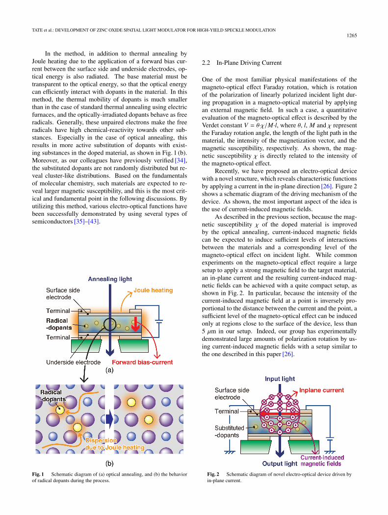
In the method, in addition to thermal annealing byJoule heating due to the application of a forward bias cur-rent between the surface side and underside electrodes, op-tical energy is also radiated. The base material must betransparent to the optical energy, so that the optical energycan efficiently interact with dopants in the material. In thismethod, the thermal mobility of dopants is much smallerthan in the case of standard thermal annealing using electricfurnaces, and the optically-irradiated dopants behave as freeradicals. Generally, these unpaired electrons make the freeradicals have high chemical-reactivity towards other sub-stances. Especially in the case of optical annealing, thisresults in more active substitution of dopants with exist-ing substances in the doped material, as shown in Fig. 1 (b).Moreover, as our colleagues have previously verified [34],the substituted dopants are not randomly distributed but re-veal cluster-like distributions. Based on the fundamentalsof molecular chemistry, such materials are expected to re-veal larger magnetic susceptibility, and this is the most crit-ical and fundamental point in the following discussions. Byutilizing this method, various electro-optical functions havebeen successfully demonstrated by using several types ofsemiconductors [35]–[43].
Fig. 1 Schematic diagram of (a) optical annealing, and (b) the behaviorof radical dopants during the process.
2.2 In-Plane Driving Current
One of the most familiar physical manifestations of themagneto-optical effect Faraday rotation, which is rotationof the polarization of linearly polarized incident light dur-ing propagation in a magneto-optical material by applyingan external magnetic field. In such a case, a quantitativeevaluation of the magneto-optical effect is described by theVerdet constant V = θ·χ/M·l, where θ, l, M and χ representthe Faraday rotation angle, the length of the light path in thematerial, the intensity of the magnetization vector, and themagnetic susceptibility, respectively. As shown, the mag-netic susceptibility χ is directly related to the intensity ofthe magneto-optical effect.
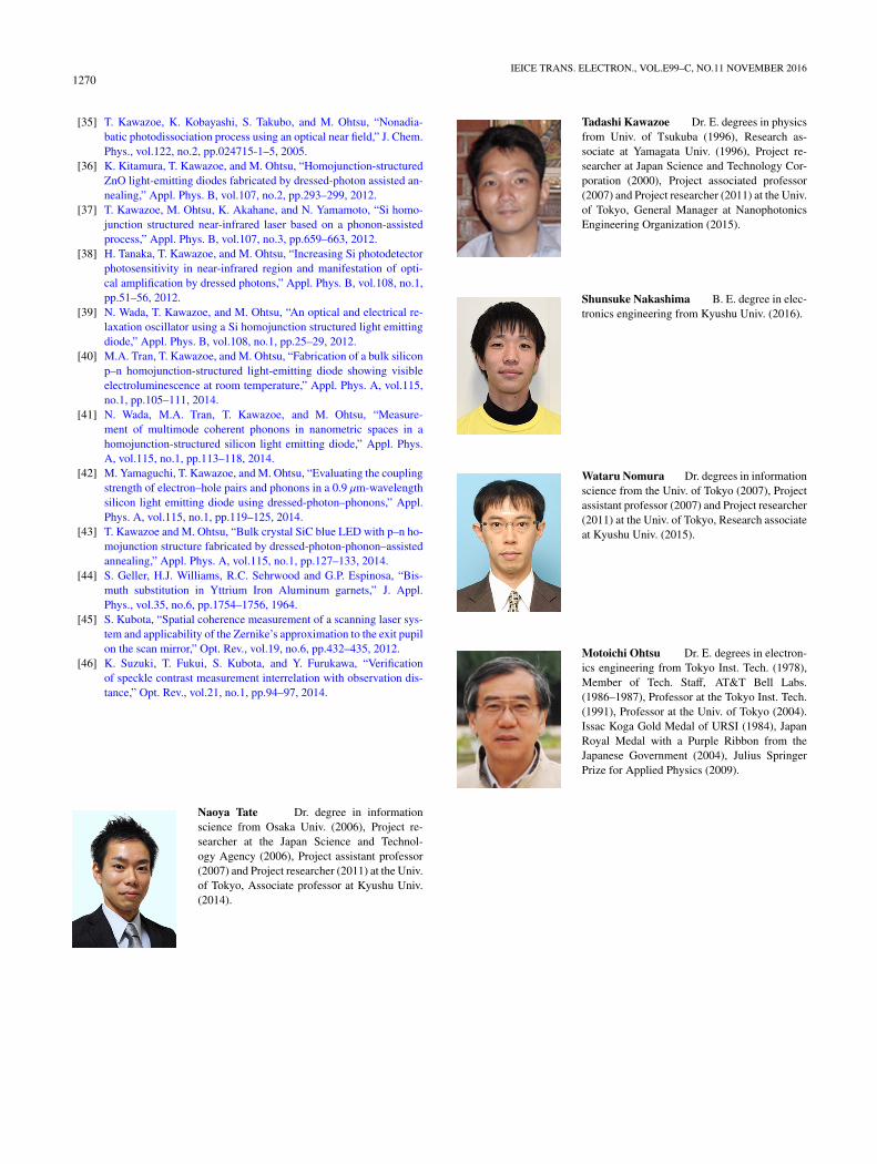
Recently, we have proposed an electro-optical devicewith a novel structure, which reveals characteristic functionsby applying a current in the in-plane direction [26]. Figure 2shows a schematic diagram of the driving mechanism of thedevice. As shown, the most important aspect of the idea isthe use of current-induced magnetic fields.
As described in the previous section, because the mag-netic susceptibility χ of the doped material is improvedby the optical annealing, current-induced magnetic fieldscan be expected to induce sufficient levels of interactionsbetween the materials and a corresponding level of themagneto-optical effect on incident light. While commonexperiments on the magneto-optical effect require a largesetup to apply a strong magnetic field to the target material,an in-plane current and the resulting current-induced mag-netic fields can be achieved with a quite compact setup, asshown in Fig. 2. In particular, because the intensity of thecurrent-induced magnetic field at a point is inversely pro-portional to the distance between the current and the point, asufficient level of the magneto-optical effect can be inducedonly at regions close to the surface of the device, less than5 μm in our setup. Indeed, our group has experimentallydemonstrated large amounts of polarization rotation by us-ing current-induced magnetic fields with a setup similar tothe one described in this paper [26].
Fig. 2 Schematic diagram of novel electro-optical device driven byin-plane current.

1266IEICE TRANS. ELECTRON., VOL.E99–C, NO.11 NOVEMBER 2016
2.3 Device Configuration
Our previous achievements that revealed giant polarizationrotation were demonstrated by using a reflective-type de-vice [26]. In order to improve the practicality of our idea,we newly developed a transmissive-type device. Similarto the previous device, a commercially available ZnO sin-gle crystal, which was prepared by the hydrothermal growthmethod, was used, and nitrogen ions were doped into thecrystal by using multi-step implantation [36]. The implanta-tion is done by sequentially applying N+ and N2+ with ac-celeration energies in six steps from 20 keV to 600 keV. Asa result, the thickness of the doped layer in the ZnO crys-tal became 2 ∼ 3 μm with a dopant density of 1018 ∼ 1019
atoms/cm3, and the depth from the surface of the device wasless than 1 μm. As the surface side and underside electrodes,150 nm-thick indium tin oxide (ITO) films were depositedby radio frequency (RF) sputtering, and Au terminals werefabricated at each side by deposition and etching processes.Then, the doped-ZnO was set on a glass epoxy substrate,and an aperture was formed to allow transmission of the in-cident light.
The surface side and underside electrodes were con-nected so as to perform optical annealing. During 16 hoursof annealing, a forward bias current with a current densityof less than 0.1 A/cm2 was applied between the surface sideand underside electrodes, which was the highest current thatcould be applied without causing any thermal destruction ofthe Au terminals. The photon energy of the annealing lightwas set at 3.05 eV, which is much lower than the bandgapenergy of ZnO (3.40 eV), and the power density of the an-nealing light focused on the device was 1 W/cm2.
After the annealing process, the electrode connectionwas changed to apply the in-plane current for driving thedevice, as shown in Fig. 3 (a). Here, the same light sourceas that used for the annealing light was used as the inputlight source, and it is linearly-polarized by Glan-Thompsonpolarizer. Due to phase shifts during the propagation in thedevice, transmitted light reveals elliptical polarization. Pho-tographs of the device are shown in Fig. 3 (b). As shown,four independent units were prepared on a single device toverify crosstalk between each unit. Each unit has four Auterminals, and the in-plane current was applied by connect-ing two arbitrary terminals of the four terminals.
3. Refractive Index Modulation
Polarization rotation based on the magneto-optical effect isone aspect of the circular-polarization selection rule towardoptical transitions in a material with high magnetization. Inother words, a difference in refractive index between left-and right-handed circularly polarized light corresponds torotation of linearly-polarized light. Although giant polar-ization rotation has been previously demonstrated by ourgroup [26], here we focus on modulation of the refractiveindex and a corresponding beam shift of plane-wave light
Fig. 3 (a) Schematic diagram of transmissive-type ZnO SLM and(b) photograph of the device consisting of 2 × 2 units.
by using a ZnO-SLM. The basics of the demonstration aredescribed in the following.
As schematically shown in Fig. 4, because a spatial dis-tribution of in-plane current density and a correspondingmagnetic field distribution can be made to occur by usingtwo terminals on the surface side electrodes of the SLM, acorresponding spatial distribution of the refractive index ofZnO is obtained. In such a case, incident plane-wave lightis refracted by the SLM. If different pairs of terminals areused, refraction in different directions is induced.
Figure 5 show the results of some demonstrations ofthe refraction of plane-wave light, where the output lightwas captured by a CCD camera when voltages of 0 V (left)and 18 V (right) were applied to the SLM. In the experi-ment, only one of the four units was driven, and only thecorresponding light, namely, the upper-right light in Fig. 5,was modulated. As shown in Figs. 5 (a) and (b), only theupper-right light was shifted in the vertical and horizontaldirections, respectively.
As we have shown, the refraction direction correspondsto the position of the terminals used for injection of the in-plane current. As a result, we verified that the spatial distri-butions of the in-plane current density and the correspond-ing magnetic fields induced a spatial distribution of the re-fractive index in the ZnO. During the demonstration shownin Fig. 5 (a), the change in the refractive index, which is ap-proximately calculated from the amount of shift of the in-

TATE et al.: DEVELOPMENT OF ZINC OXIDE SPATIAL LIGHT MODULATOR FOR HIGH-YIELD SPECKLE MODULATION1267
Fig. 4 Schematic diagram of spatial distribution of refractive index dueto spatial distribution of in-plane current density (upper), and correspond-ing beam shift of incident plane-wave light (lower).
Fig. 5 Experimental results of refraction of plane-wave light in(a) vertical direction and (b) horizontal direction.
cident light, depends on the voltage applied to the SLM, asshown in Fig. 6.
As shown, a change in refractive index of up to 0.40,which is 5% of the change rate relative to the default refrac-tive index of ZnO crystal (2.00) at room temperature, wasobtained by applying a voltage of 20 V. This change is ex-tremely large as compared to that in well-known magneto-
Fig. 6 Change in refractive index.
Fig. 7 Directions and amounts of refraction by using various pairs ofterminals with (a) annealed unit and (b), (c), (d) non-annealed units. Ter-minal 2 is used during the optical annealing process.
optical materials, such as yttrium iron garnet (YIG) [44].Moreover, various directions and amounts of refraction
obtained by using various pairs of terminals are shown inFig. 7. Figure 7(a) shows a case where an annealed unit isused, and Figs. 7 (b), (c), and (d) shows cases where non-annealed units are used. The squares and number in eachsquare represent the positions and serial numbers identify-ing terminals of the surface side electrode, respectively, andthe underlined numbers represent the used pairs of termi-nals.
As shown, the amounts of shift and the shift direc-tions with the non-annealed units were more non-uniform,

1268IEICE TRANS. ELECTRON., VOL.E99–C, NO.11 NOVEMBER 2016
Fig. 8 (a) Schematic diagram of optical setup for experimental demon-stration of speckle modulation, and (b) the results of speckle modulation.
whereas more uniform refraction was obtained with the an-nealed unit. The results indicate that optical annealing real-izes homogeneously-distributed dopants, so that the spatialdistribution of the refractive index is homogeneously modu-lated by using any pairs of terminals.
4. Speckle Modulation
We experimentally demonstrated the speckle modulationbase on the beam shifts. Because speckle patterns are partic-ular to the surface roughness at each focal point on a target,beam shifts due to the spatial distribution of the refractiveindex induce various speckle patterns. By modulating thespeckle patterns at sufficiently high speed, the contrast ofa time-averaged image of the patterns is lower than that ofindividual patterns.
Figure 8 (a) shows the experimental setup used fordemonstrating speckle modulation. Similarly to the previ-ous demonstrations, plane-wave light from a laser source isinput to the SLM and is focused on a frosted diffuser to gen-erate speckle patterns. The surface roughness parameter ofthe diffuser is �1,000.
The focused point of light is shifted by modulation withthe SLM, and the speckle patterns generated by the diffuserare correspondingly modulated. The speckle patterns ob-tained by the CCD camera are shown in Fig. 8 (b). The volt-age applied to the SLM as a modulation signal was a saw-tooth wave varying from 12 V to 24 V. A bias voltage of 12V was applied so as to use the linear region of the modula-tion characteristic shown in Fig. 6.
For quantitative evaluation of our method, the speckle
Fig. 9 Reduction of speckle contrast by using ZnO-SLM.
contrast is calculated from trimmed images obtained fromvideo captured by the CCD camera. Here, we obtained a30 ms time-averaged image, which can be observed by thehuman eye. The result is shown in Fig. 9.
As shown, the speckle contrast was successfully re-duced from 0.67 to 0.46. However, the amounts seem toconverge to a constant value in the result. This is consid-ered to be due to the polarization selectivity of the magneto-optical effect of the SLM. Namely, because only one direc-tion of circularly polarized light was modulated by the SLMand the other was not, unmodulated speckle patterns re-mained in the time-averaged image. Thus, speckle contrastcannot be reduced to a sufficient value required for actualuse as speckle reduction device, namely, less than 0.10. Theresult indicates that polarization control of the laser sourceis important for realizing speckle reduction with our SLM.
As a matter of fact, the results in Fig. 9 only indicatesrelative changes of speckle patterns induced by our specificsetup. As further studies, in order to more strictly discussthe speckle reduction, adopting more general methods forthe measurement of speckle contrast must be required [45],[46].
5. Conclusion
As shown, we described the development of a specially de-signed SLM, namely, a transmissive-type ZnO-SLM. Sim-ilarly to the authors’ previous approach [26], the SLM isfabricated by using optical annealing and is driven by ap-plying an in-plane current, which induces magnetic fields.The results of experimental demonstrations revealed largemodulation of the spatial distribution of the refractive index.Moreover, for the future application to the speckle reduc-tion, we focused on high-speed modulation of speckle pat-terns by utilizing beam shifts of incident plane-wave lightdue to modulation of the spatial distribution of the refractiveindex. While the conventional approaches [11]–[25] requirea mechanical setup to realize high-speed fluctuation of thedisplayed screen, the main advantage of our idea is the highspeed achieved by a compact setup that does not require anymechanical elements, which lower the stability and durabil-

TATE et al.: DEVELOPMENT OF ZINC OXIDE SPATIAL LIGHT MODULATOR FOR HIGH-YIELD SPECKLE MODULATION1269
ity of the conventional set-ups.Moreover, the basic mechanism of our method is the
magneto-optical effect brought about by current-inducedmagnetic fields. As is well-known, the basic geometry of themagneto-optical effect is defined by spin flips of electrons ina nanometric space, which are induced in processing timesof less than ps-order. Therefore, a compact, high-speed sys-tem for speckle reduction can be implemented. In future re-search, we are planning to quantitatively verify the responsecharacteristics of the modulation and optimize the specifi-cations of the device so that it can be applied to practicalspeckle reduction for laser displays in the near future.
This work was supported by a research grant from TheMurata Science Foundation and by Kyushu University Inter-disciplinary Programs in Education and Projects in ResearchDevelopment.
References
[1] J.W. Goodman, Speckle Phenomena in Optics, W.H. Freeman, 2010.[2] N. George and A. Jain, “Speckle reduction using multiple tones of
illumination,” Appl. Opt., vol.12, no.6, pp.1202–1212, 1973.[3] C. Saloma, S. Kawata, and S. Minami, “Laser-diode microscope
that generates weakly speckled images,” Opt. Lett., vol.15, no.4,pp.203–205, 1990.
[4] B. Dingel and S. Kawata, “Laser-diode microscope with fiber illu-mination,” Opt. Comm., vol.93, no.1-2, pp.27–32, 1992.
[5] B. Dingel and S. Kawata, “Speckle-free image in a laser-diode mi-croscope by using the optical feedback effect,” Opt. Lett., vol.18,no.7, pp.549–551, 1993.
[6] A. Furukawa, N. Ohse, Y. Sato, D. Imanishi, K. Wakabayashi,S. Itoh, K. Takamura, and S. Hirata, “Effective speckle reductionin laser projection display,” Proc. SPIE, vol.6911, pp.69110T-1–7,2008.
[7] F. Riechert, G. Craggs, Y. Meuret, B. van Giel, H. Thienpont, U.Lemmer, and G. Verschaffelt, “Low-speckle laser projection witha broad-area vertical-cabity surface-emitting laser in the nonmodalemission regime,” Appl. Opt., vol.48, no.4, pp.792–798, 2009.
[8] H. Murata, K. Furushoi, Z. Yamamoto, and Y. Okamura, “Newspeckle control technique using high-speed electro-optic modulatorswith resonant electrode and polarization-reversed structures,” Opt.Rev., vol.19, no.6, pp.436–439, 2012.
[9] J.G. Manni and J.W. Goodman, “Versatile method for achieving1 % speckle contrast in large-venue laser projection displays us-ing a stationary multimode optical fiber,” Opt. Exp., vol.20, no.10,pp.11288–11315, 2012.
[10] H. Murata, K. Shibasaki, Z. Yamamoto, and Y. Okamura, “Specklecontrol using high-frequency signal superposition to semiconductorlaser,” Opt. Rev., vol.21, no.1, pp.79–82, 2014.
[11] S. Lowenthal and D. Joyeux, “Speckle removal by slowly movingdiffuser associated with a motionless diffuser,” J. Opt. Soc. Am.,vol.61, no.7, pp.847–851, 1971.
[12] E.G. Rawson, A.B. Nafarrate, R.E. Norton, and J.W. Goodman,“Speckle-free rear-projection screen using two close screens in slowrelative motion,” J. Opt. Soc. Am., vol.66, no.11, pp.1290–1294,1976.
[13] H. Amber, Y. Aoki, N. Takai, and T. Asakura, “Mechanism ofspeckle reduction in laser-microscope-images using a rotating op-tical fiber,” Appl. Phys. B, vol.38, no.1, pp.71–78, 1985.
[14] T. Yoshimura and K. Fujiwara, “Statistical properties of doubly scat-tered image speckle,” J. Opt. Soc. Am. A, vol.9, no.1, pp.91–95,1992.
[15] L. Wang, T. Tschudi, T. Halldorsson, and P.R. Petursson, “Specklereduction in laser projection system by diffractive optical elements,”
Appl. Opt., vol.37, no.10, pp.1770–1775, 1998.[16] K. Kasazumi, Y. Kitaoka, K. Mizuuchi, and K. Yamamoto, “A prac-
tical laser projector with new illumination optics for reduction ofspeckle noise,” Jpn. J. Appl. Phys., vol.43, no.8B, pp.5904–5906,2004.
[17] S.C. Shin, S.S. Yoo, S.Y. Lee, C.-Y. Park, S.-Y. Park, J.W. Kwon, andS.-G. Lee, “Removal of hot speckle on rear projection screen usingthe rotating screen system,” J. Disp. Tech., vol.2, no.1, pp.79–84,2006.
[18] I. Fujieda, T. Kosugi, and Y. Inaba, “Speckle noise evaluation andreduction of an edge-lit backlight system utilizing laser diodes andan optical fiber,” J. Disp. Tech., vol.5, no.11, pp.414–417, 2009.
[19] S. An, A. Lapchuk, V. Yurlov, J. Song, H. Park, J. Jang, W. Shin,S. Kargapoltsev, and S.K. Yun, “Speckle suppression in laser dis-play using several partially coherent beams,” Opt. Exp., vol.17, no.1,pp.92–103, 2009.
[20] Y. Kuratomi, K. Sekiya, H. Satoh, T. Tomiyama, T. Kawakami, B.Katagiri, Y. Suzuki, and T. Uchida, “Speckle reduction mechanismin laser rear projection displays using a small diffuser,” J. Opt. Soc.Am. A, vol.27, no.8, pp.1812–1817, 2010.
[21] G. Ouyang, Z. Tong, M.N. Akram, K. Wang, V. Kartashoc, X. Yan,and X. Chen, “Speckle reduction using a motionless diffractive op-tical element,” Opt. Lett., vol.35, no.17, pp.2852–2854, 2010.
[22] M. Kurashige, K. Ishida, T. Takanokura, Y. Ohyagi, and M.Watanabe, “The evaluation of speckle contrast with variable specklegenerator,” J. Soc. Inf. Display, vol.19, no.9, pp.631–638, 2011.
[23] Z. Tong, X. Xhen, M.N. Akram, and A. Aksnes, “Compound specklecharacterization method and reduction by optical design,” J. Disp.Tech., vol.8, no.3, pp.132–137, 2012.
[24] C.-Y. Chen, W.-C. Su, C.-H. Lin, M.-D. Ke, Q.-L. Deng, and K.-Y.Chiu, “Reduction of speckles and distortion in projection system byusing a rotating diffuser,” Opt. Rev., vol.19, no.6, pp.440–443, 2012.
[25] T.-K.-T. Tran, S. Subramaniam, C.-P. Le, S. Kaur, S. Kalicinski,M. Ekwinska, E. Halvorsen, and M.N. Akram, “Design, modeling,and characterization of a microelectromechanical diffuser device forlaser speckle reduction,” J. Microelectromech. Sys., vol.23, no.1,pp.117–127, 2014.
[26] N. Tate, T. Kawazoe, W. Nomura, and M. Ohtsu, “Current-inducedgiant polarization rotation using a ZnO single crystal doped with ni-trogen ions,” Scientific Reports, vol.5, Article number 12762, 2015.
[27] U. Ozgur, Y.I. Alivov, C. Liu, A. Teke, M.A. Reshchikov, S.Dogan, V. Avrutin, S.-J. Cho, and H. Morkoc, “A comprehensivereview of ZnO materials and devices,” J. Appl. Phys., vol.98, no.4,pp.041301-1–103, 2005.
[28] N. Yamazoe, “New approaches for improving semiconductor gassensors,” Sens. Actuators B: Chem., vol.5, no.1-4, pp.7–19, 1991.
[29] K.D. Schierbaum, U. Weimar, and W. Gopel, “Comparison of ce-ramic, thick film, and thin film chemical sensors based upon SnO2,”Sens. Actuators B: Chem., vol.7, no.1-3, pp.709–716, 1992.
[30] G. Kiss, Z. Pinter, I.V. Perczel, Z. Sassi, and F. Reti, “Study of oxidesemiconductor sensor materials by selected methods,” Thin SolidFilms, vol.391, no.2, pp.216–223, 2001.
[31] K. Nomura, H. Ohta, A. Takagi, T. Kamiya, M. Hirano, andH. Hosono, “Room-temperature fabrication of transparent flexiblethin-film transistors using amorphous oxide semiconductors,” Na-ture, vol.432, no.7016, pp.488–492, 2004.
[32] J.S. Park, W.-J. Maeng, H.-S. Kim, and J.-S. Park, “Review of recentdevelopments in amorphous oxide semiconductor thin-film transis-tor devices,” Thin Solid Films, vol.520, no.6, pp.1679–1693, 2012.
[33] T. Kawazoe, M.A. Mueed, and M. Ohtsu, “Highly efficient andbroadband Si homojunction structured near-infrared light emittingdiodes based on the phonon-assisted optical near-field process,”Appl. Phys. B, vol.104, no.4, pp.747–754, 2011.
[34] T. Kawazoe, K. Nishioka, and M. Ohtsu, “Polarization control of aninfrared silicon light-emitting diode by dressed photons and analysesof the spatial distribution of doped Boron atoms,” Appl. Phys. A,vol.121, no.4, pp.1409–1415, 2015.
1270IEICE TRANS. ELECTRON., VOL.E99–C, NO.11 NOVEMBER 2016
[35] T. Kawazoe, K. Kobayashi, S. Takubo, and M. Ohtsu, “Nonadia-batic photodissociation process using an optical near field,” J. Chem.Phys., vol.122, no.2, pp.024715-1–5, 2005.
[36] K. Kitamura, T. Kawazoe, and M. Ohtsu, “Homojunction-structuredZnO light-emitting diodes fabricated by dressed-photon assisted an-nealing,” Appl. Phys. B, vol.107, no.2, pp.293–299, 2012.
[37] T. Kawazoe, M. Ohtsu, K. Akahane, and N. Yamamoto, “Si homo-junction structured near-infrared laser based on a phonon-assistedprocess,” Appl. Phys. B, vol.107, no.3, pp.659–663, 2012.
[38] H. Tanaka, T. Kawazoe, and M. Ohtsu, “Increasing Si photodetectorphotosensitivity in near-infrared region and manifestation of opti-cal amplification by dressed photons,” Appl. Phys. B, vol.108, no.1,pp.51–56, 2012.
[39] N. Wada, T. Kawazoe, and M. Ohtsu, “An optical and electrical re-laxation oscillator using a Si homojunction structured light emittingdiode,” Appl. Phys. B, vol.108, no.1, pp.25–29, 2012.
[40] M.A. Tran, T. Kawazoe, and M. Ohtsu, “Fabrication of a bulk siliconp–n homojunction-structured light-emitting diode showing visibleelectroluminescence at room temperature,” Appl. Phys. A, vol.115,no.1, pp.105–111, 2014.
[41] N. Wada, M.A. Tran, T. Kawazoe, and M. Ohtsu, “Measure-ment of multimode coherent phonons in nanometric spaces in ahomojunction-structured silicon light emitting diode,” Appl. Phys.A, vol.115, no.1, pp.113–118, 2014.
[42] M. Yamaguchi, T. Kawazoe, and M. Ohtsu, “Evaluating the couplingstrength of electron–hole pairs and phonons in a 0.9 μm-wavelengthsilicon light emitting diode using dressed-photon–phonons,” Appl.Phys. A, vol.115, no.1, pp.119–125, 2014.
[43] T. Kawazoe and M. Ohtsu, “Bulk crystal SiC blue LED with p–n ho-mojunction structure fabricated by dressed-photon-phonon–assistedannealing,” Appl. Phys. A, vol.115, no.1, pp.127–133, 2014.
[44] S. Geller, H.J. Williams, R.C. Sehrwood and G.P. Espinosa, “Bis-muth substitution in Yttrium Iron Aluminum garnets,” J. Appl.Phys., vol.35, no.6, pp.1754–1756, 1964.
[45] S. Kubota, “Spatial coherence measurement of a scanning laser sys-tem and applicability of the Zernike’s approximation to the exit pupilon the scan mirror,” Opt. Rev., vol.19, no.6, pp.432–435, 2012.
[46] K. Suzuki, T. Fukui, S. Kubota, and Y. Furukawa, “Verificationof speckle contrast measurement interrelation with observation dis-tance,” Opt. Rev., vol.21, no.1, pp.94–97, 2014.
Naoya Tate Dr. degree in informationscience from Osaka Univ. (2006), Project re-searcher at the Japan Science and Technol-ogy Agency (2006), Project assistant professor(2007) and Project researcher (2011) at the Univ.of Tokyo, Associate professor at Kyushu Univ.(2014).
Tadashi Kawazoe Dr. E. degrees in physicsfrom Univ. of Tsukuba (1996), Research as-sociate at Yamagata Univ. (1996), Project re-searcher at Japan Science and Technology Cor-poration (2000), Project associated professor(2007) and Project researcher (2011) at the Univ.of Tokyo, General Manager at NanophotonicsEngineering Organization (2015).
Shunsuke Nakashima B. E. degree in elec-tronics engineering from Kyushu Univ. (2016).
Wataru Nomura Dr. degrees in informationscience from the Univ. of Tokyo (2007), Projectassistant professor (2007) and Project researcher(2011) at the Univ. of Tokyo, Research associateat Kyushu Univ. (2015).
Motoichi Ohtsu Dr. E. degrees in electron-ics engineering from Tokyo Inst. Tech. (1978),Member of Tech. Staff, AT&T Bell Labs.(1986–1987), Professor at the Tokyo Inst. Tech.(1991), Professor at the Univ. of Tokyo (2004).Issac Koga Gold Medal of URSI (1984), JapanRoyal Medal with a Purple Ribbon from theJapanese Government (2004), Julius SpringerPrize for Applied Physics (2009).