Embed Size (px)
Citation preview

1
Development of residual stress in sol-gel derived Pb(Zr,Ti)O3 films: An
experimental study
S. Corkovic, Q. Zhang
Department of Materials, Cranfield University, Bedfordshire, United Kingdom MK43 0AL
Abstract
Residual stresses develop in the sol-gel-derived ferroelectric thin films during the
transformation of the metalorganic gel to the metal oxide upon thermal treatment and due to
the thermal and elastic mismatch between the Pb(Zrx,Ti1-x)O3 (PZT) film and the substrate
materials during cooling. In this study, residual stresses were determined using the wafer
curvature method after the deposition of multilayer PZT film on platinized (100) silicon
wafers. A multilayer model for stress analysis was used to calculate the residual stress in PZT
films of three different compositions, x=0.4, x=0.52 and x=0.6. Orientation dependent
residual stresses were found in compositions containing the tetragonal phase, with x=0.4 and
x=0.52. Depending on the fraction of (100) orientated domains low compressive or low
tensile stress was found in Pb(Zr0.4Ti0.6)O3 (PZT 40/60). Higher residual stress was found in
PZT films consisting of only rhombohedral crystallographic structure (PZT 60/40) while the
residual stress in PZT films with morphotropic boundary composition (PZT 52/48) was
significantly dependent on the film orientation and the phase composition and could range
from 17 MPa to 90 MPa. The effect of the film orientation on residual stress was found to be
a function of the anisotropic thermal expansion coefficient of PZT. The contribution of the
thermal and elastic properties of materials to the total wafer curvature was investigated and
discussed. Finally, the residual stress results calculated with the four layers model were
compared to the results calculated using the Stoney equation.

2
1. Introduction
Among the available ferroelectric materials, lead zirconate titanate Pb(ZrxTi1-x)O3 (PZT), is
the most popular due to its superior dielectric, piezoelectric properties, and good thermal
stability [1]. The applications of PZT films in microelectromechanical systems (MEMS)
devices exploiting the piezoelectric effect open up new possibilities in on-chip
implementation [2-4].
The demand of the residual stress characterization arises from the requirement of
stress-free MEMS structures since the residual film stress can cause the device bending, as
shown by Zhang et al [5]. The effects of residual stresses on the properties of thin films have
been widely studied, for example, the effects of the residual stress on the ferroelectric and
piezoelectric properties [6-8]; the effects of strain on the crystallographic orientation of the
film when passing through the transition temperature [9-10]; the effects of applied stress on
the ferroelectric properties [11-14] and the effect of stress on the phase shift at the
morphotropic phase boundary compositions [15].
The residual stress characterization of Chemical Solution Deposition (CSD) derived
PZT thick films was a subject of many investigations, first reported for CSD derived thick
films by Yi and Sayer [16]. The intrinsic stress develops in CSD films during heat treatment
as a result of solvent evaporation and leads to the shrinkage of the film. The pyrochlore-to-
perovskite transformation was associated with large stress [17] that accounts for the major
fraction of the residual stress, around 100 MPa. Ong and Payne [18] investigated the stress
during processing of single and multilayer films and showed that the values of residual stress
in films at different PZT thickness were between 120 and 140 MPa. However, in their work
PZT was deposited on silicon rather than on platinum. Spierings et al [19] reported on the
development of residual stress in the sol-gel deposited PZT 50/50 films and argued that the
nature of stress in PZT is due to thermal expansion mismatch between PZT and the bottom (or

3
the top) electrode which could be explained in more detail if the anisotropic thermal
expansion of PZT is considered. The stress relaxation mechanism of the domain formation at
the phase transition was first reported by Roitburd [20] which was further developed by Speck
and Pompe [21-22] and Pertsev [23] for epitaxial thin films by calculating the
thermodynamically stable domain configuration dependent on the thermal strain difference
between the film and the substrate. Roitburd and Kosenko [24] reported also on the
orientation dependence of the elastic energy during phase formation which can be applied to
the pyrochlore-perovskite transformation.
A detailed stress analysis in sputter deposited PZT films can be found in work of
Bruchhaus et al [25-27]. Bruchhaus et al illuminated the stress development in the bottom
electrode (Pt/TiO2) and investigated the stress development during the pyrochlore-perovskite
transformation in PZT films of various compositions.
The research activities regarding the residual stress characterization in PZT films and
the influence of the stress on the electrical properties rapidly increased in last few years.
Although much work has focused on residual stress in CSD PZT films [28-29], the
understanding of the stress development that leads to residual stress is intermittent,
particularly in the transition of the wet films to the crystallization. Further, to identify and
design a stress-free device structure, it is important to identify the contribution of all layers to
the total stress.
The purpose of this study is to shed light on the stress development during the whole
processing of PZT film formation, from as-deposited wet film to its crystallization at high
temperature and thereafter to cooling down to the room temperature. It addresses the main
stages at which the major stress can be developed or relaxed in CSD derived films. For this
reason a non-conventional approach to stress calculation in thin films was adopted. This
approach includes the stress calculation with a multilayer model where thermal and elastic
properties of each layer are considered, the wafer curvature calculation modeling and

4
comparative, or where otherwise not possible, stress calculation using the Stoney equation.
Such analysis allowed identifying and separating the processes in the substrate and the PZT
films which affect the residual stress in the PZT films.
2. Experimental
2.1 Prior to any film processing the blank wafer displacement of all samples was measured
using the Veeco Dektak Surface Profilometer. For some preliminary characterization of the
wafer curvature the wafer displacement was measured in several equidistant and parallel lines
across the wafer surface. The starting point for each scan was set along one line parallel to the
primary flat of the wafer. Then the same wafer was rotated for 90° and the same kind of
displacement measurement was performed in the direction perpendicular to the first set of
scans. The scan length was always higher than 50% of the total diameter of the wafer.
2.2 The sol precursor preparation and film processing were reported in detail in [17]. Here,
only a brief description will be given. Three different sol compositions were used: PZT 40/60,
PZT 52/48 and PZT 60/40. The single layer thickness was 200 nm for all films. Thicker films
(referred to as multilayer films) were fabricated by repeated spin-coating. All films were
processed at four distinct temperatures, 100°C, 300°C, 460°C and 550°C (or 630°C for the
PZT 60/40 films). The PbO sol was made by dissolving Lead-2-ethylhexanoate in ethanol.
The PZT films were deposited on platinized silicon substrates. A Pt/Ti bilayer (100nm/8nm)
was sputter deposited onto all substrates. Three different sizes of the silicon (100) substrates
were employed: 2", 3" and 4" wafers. 2" silicon wafers were thermally oxidized to grow a 600
nm thick SiO2 diffusion barrier layer. All other silicon wafers were commercially supplied
with a 450 nm thick SiO2 layer. In two samples only a native oxide layer was employed. Ten
different samples were fabricated for the stress analysis. Their details are summarized in Tab.
I.

5
2.3 For the residual stress characterization a wafer curvature measurements were performed
always along the same line across the wafer using a self designed and constructed jig to assure
the accuracy of the measurement. The wafer curvature was always measured on a blank wafer
before platinum deposition, after platinum deposition, after platinum annealing, and after each
PZT layer was completely crystallized.
2.4 For four experiments the wafer deflection was measured after heating the sample on a
hotplate at given temperatures, in the temperature range between 100 ºC and 550 ºC. Each
sample was heated e.g. at 100°C for 1 minute and cooled down to room temperature followed
by a wafer deflection measurement. The temperature of a hotplate was increased for 25°C and
the same cycle of heating the sample for 1 minute, cooling it down to room sample and
measuring the wafer curvature was performed until the last heating temperature (550°C) was
reached. Two experiments were performed on bare platinized silicon substrates; one substrate
having an 8 nm thin Ti adhesion layer with following dimensions: Pt/Ti/SiO2/Si
(100nm/8nm/~10nm/525micron) and the other substrate was identical expect for the Ti layer
which was not deposited. For the two other experiments a single layer of PZT 40/60 (200nm)
was coated on the Pt/Ti/Si substrate, with the difference that one substrate was pre-annealed at
550°C for 30 minutes and the other was not.
2.5 The orientation of each film was determined by the standard θ–2θ X-ray diffraction
(XRD) method on a Siemens D5005 diffractometer using CuKα radiation and a Goebel
mirror. The peaks were deconvoluted and the integral intensities were determined for all
detected peaks. The peak intensities were normalized according to [30] and compared with
the powder diffraction files from the PCPDF database. The crystallite size was determined
using the Scherrer equation:
coscB
k (1)

6
where is crystallite size, k is a parameter between 0.8 and 1, c is full width at half peak
maxima.
3. Stress analysis methods
3.1 Model for composite structures
A model derived by Townsend et al [31] was employed to calculate and analyze the curvature
evolution and the residual stress from the curvature measurements in multilayer PZT films.
This model was derived for composite structures and takes into account different mechanical
and thermal expansion properties of each layer in composite structure. The details are given in
Ref. [31], and here only the used equations are reproduced.
Based on the strength of materials approach the stress in each layer can be calculated
using the following equation:
Kz
tE
TdtE
TdE
jjj
jjjjj
iiii )(
))(ln(
))(ln(0,
0,
(2)
whereby Ei, i and ti are the biaxial elastic modulus, the thermal expansion coefficient and the
thickness of the layer i, respectively; di,0 the length or diameter of the layer I before the
temperature change T; the position of the neutral plane, K the composite curvature and z
the distance from the bottom of the composite structure to the top surface of the layer i. As
stated in Ref. [31] it is required for all layers of the composite structure to have equal length at
the point before the temperature changes. Whether such condition of the composite structure
in PZT films exists or not will be discussed in the following sections.

7
Furthermore, this stress analysis approach allows curvature calculation by requesting a
zero net moment and thus results in the following equation
iii
iii
i
jjj
jjjj
ii
ii
ttttt
tE
tE
tEt
ET
K222
2
312
1
232
2
. (3)
For details of the Eq. (3) please see the Ref. [31].
A residual stress model was designed to allow stress calculations in four layers, in particular
for the following structure Si/SiO2/Pt/PZT. The calculation of the stress in the silicon oxide
layer was neglected if the silicon oxide was thinner than 50 nm. All required parameters for
the calculations such as layer thickness and wafer length were measured except for the
thermal expansion coefficients (TEC) and elastic moduli which were taken from diverse
sources from the literature. The TECs for investigated PZT compositions were calculated
using the thermal expansion data given in Ref. [32-34] for PZT 70/30, PZT 50/50 and PZT
48/52 respectively. The non-linear thermal expansion for silicon, platinum and silicon oxide
were taken from Ref. [35]. The TECs of all individual layers as used in the calculations are
shown in Fig. 1 and their average values are summarized in Tab. II.
The wafer curvature was calculated for every displacement measurement and in
discrete points along the scan profile using

8
2
32 )'1(
'')(
y
yxK
(4)
where y' was a polynomial function of 6th order applied to the curvature profile. y'
and y" were first and second derivates of the function y.
3.2 Stoney equation
For some particular experiments it was not possible to calculate the stress via the model
introduced in 3.1 since the thermal or elastic properties are not known e.g. of the wet PZT
layer or where a non-elastic deformation was found, such as in platinum layer immediately
after deposition. In this case the more common Stoney equation was applied
f
sprepost
t
tEKK
6)1()(
2
(5)
where Kpre, Kpost is the wafer curvature before and after the film, respectively; E, and ts the
elastic modulus, Poison’s ratio, the thickness of the substrate respectively, and tf the film
thickness. In addition, the residual stress results obtained with the Eq. (2) were compared
against the stress results calculated with the Stoney equation.
4. Results and discussion
4.1 Preliminary characterizations
The residual stress characterization based on the curvature measurement has been recently
debated whether the film stress is isotropic and uniform as it is required when using e.g. the
Stoney equation [39] for stress calculation [40-43]. To calculate the residual stress from the
wafer curvature measurements it is required to characterize the uniformity of the wafer

9
curvature since both approaches to stress calculation, the Stoney equation and the Eq. (2), are
based on the linear and uniform beam deformation. Thus, strong deviations of curvature
across the wafer surface can result in large differences in the stress values. To clarify the
shape of the wafer bending due to film stress the curvature measurements were performed
according to Section 2.1. Fig. 2 shows the results of the normalized curvature of such scan for
a 2" wafer after subtraction of the bare silicon wafer curvature. A cup-shape of the wafer was
observed and it showed a fairly radial bending of the platinized silicon wafer after 1m thick
PZT film was deposited. The cup-shape was related to the anisotropic bending of the wafer
indicating a non-uniform curvature. An area of the largest curvature was found slightly off the
centre of the wafer, most likely as a result of the shift of the centre of gravity due to the
primary and secondary flats on the wafer. However, the wafer deformation was much smaller
compared to wafer thickness allowing the calculation of stress by Eq. (2) or Stoney equation.
Thus, the residual stress analysis was restricted only to the area of the maximum curvature
where maximum stress was found.
A similar experiment but on a 4" platinised silicon wafer was also conducted. After 1 m
thick PZT film was deposited, the wafer bending showed a saddle-shape (Fig. 3), indicating
much more pronounced anisotropic bending of the substrate. Thus, strong variation of the
curvature was found which makes the stress characterization more complicated when using
the 4" wafer. Again, the stress calculation was limited to the central area of the wafer where
the wafer curvature is fairly uniform. Nevertheless higher curvature and high stress can occur
at some areas close to the edges of the wafer where the film cracking was sometimes observed
when PZT was deposited onto a 4 " silicon wafer.
4.2 Stress in the bottom electrode
10
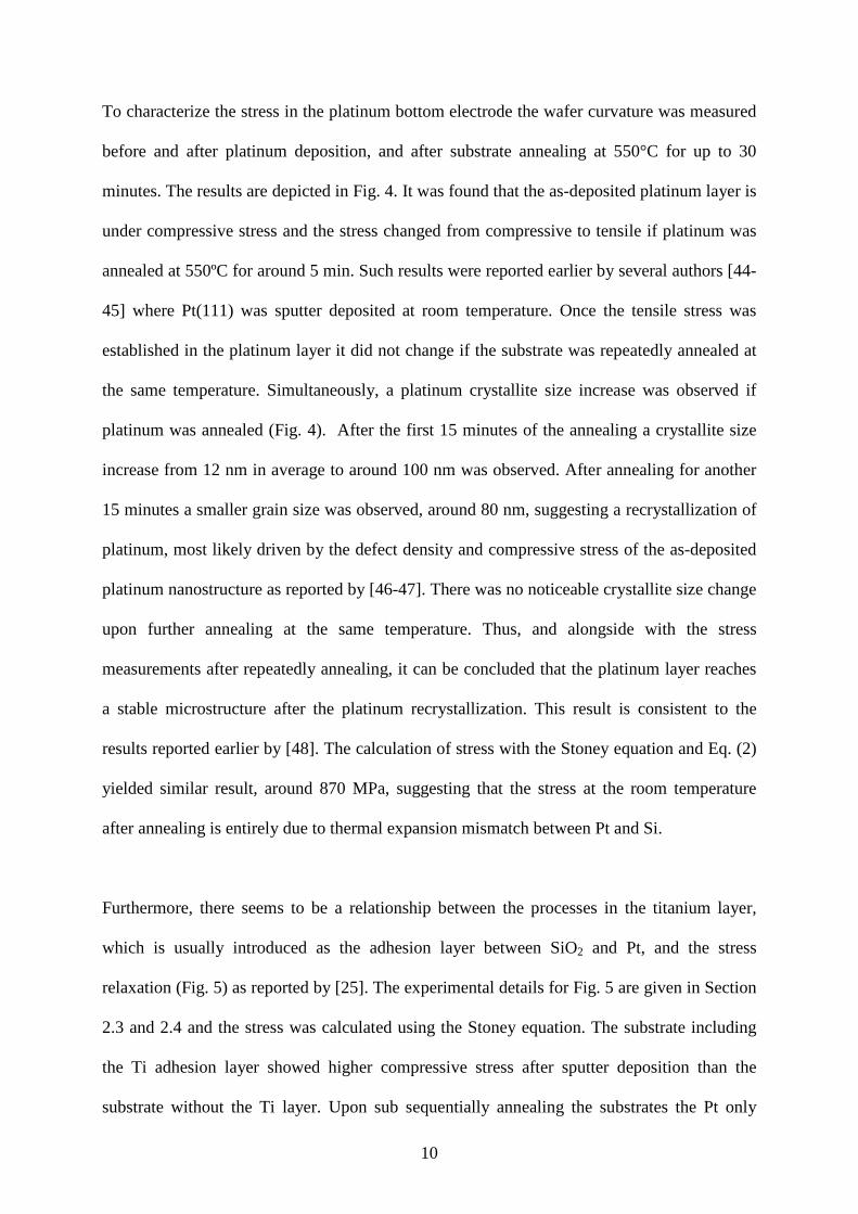
To characterize the stress in the platinum bottom electrode the wafer curvature was measured
before and after platinum deposition, and after substrate annealing at 550°C for up to 30
minutes. The results are depicted in Fig. 4. It was found that the as-deposited platinum layer is
under compressive stress and the stress changed from compressive to tensile if platinum was
annealed at 550ºC for around 5 min. Such results were reported earlier by several authors [44-
45] where Pt(111) was sputter deposited at room temperature. Once the tensile stress was
established in the platinum layer it did not change if the substrate was repeatedly annealed at
the same temperature. Simultaneously, a platinum crystallite size increase was observed if
platinum was annealed (Fig. 4). After the first 15 minutes of the annealing a crystallite size
increase from 12 nm in average to around 100 nm was observed. After annealing for another
15 minutes a smaller grain size was observed, around 80 nm, suggesting a recrystallization of
platinum, most likely driven by the defect density and compressive stress of the as-deposited
platinum nanostructure as reported by [46-47]. There was no noticeable crystallite size change
upon further annealing at the same temperature. Thus, and alongside with the stress
measurements after repeatedly annealing, it can be concluded that the platinum layer reaches
a stable microstructure after the platinum recrystallization. This result is consistent to the
results reported earlier by [48]. The calculation of stress with the Stoney equation and Eq. (2)
yielded similar result, around 870 MPa, suggesting that the stress at the room temperature
after annealing is entirely due to thermal expansion mismatch between Pt and Si.
Furthermore, there seems to be a relationship between the processes in the titanium layer,
which is usually introduced as the adhesion layer between SiO2 and Pt, and the stress
relaxation (Fig. 5) as reported by [25]. The experimental details for Fig. 5 are given in Section
2.3 and 2.4 and the stress was calculated using the Stoney equation. The substrate including
the Ti adhesion layer showed higher compressive stress after sputter deposition than the
substrate without the Ti layer. Upon sub sequentially annealing the substrates the Pt only

11
coated substrate showed a gradual change of stress from compressive to tensile while the
Pt/Ti showed an abrupt change of stress at around 425°C from compressive to tensile. Such
abrupt change of stress in about the same temperature range was reported by Bruchhaus at el
[25] while oxidizing the Ti layer to TiO2. Thus, the stress change in the bottom electrode
during annealing has two contributions and can be associated with a Ti oxidation on one hand
and with the platinum grain growth and recrystallization on the other hand.
4.3 Stress development during processing of the PZT film
The stress development in a 200 nm PZT 40/60 film on a pre-annealed and on an as-deposited
substrate is depicted in Fig. 6. The details of the process characterization in the film are
reported elsewhere [17]. The residual stress was calculated using the Stoney equation taking
the wafer curvature of platinum as a reference whereby the PZT film thickness measurement
was performed prior to every wafer curvature measurement with the same piece of equipment.
The details of thickness reduction during processing are given in Ref. [49]. One (Pt/Ti)/Si
substrate was annealed for 30 min at 550 ºC before a PZT layer was spin-coated and is
referred to as the pre-annealed substrate. The graph from Fig. 5 on the stress evolution in
annealed Pt is included for comparison.
Several stages during PZT processing can induce or relax strain. The first stage in the
CSD processing is the stage of the solvents evaporation associated with large thickness
shrinkage of the PZT film, usually at below 300 ºC. However, only after the PZT film was
treated at above 200°C the tensile stress was forming in the PZT film. Based on the earlier
findings reported in [49] a strong thickness shrinkage of the films was observed especially in
the temperature range between 100°C and 200°C and further on, it was much larger than the
lateral shrinkage. While the wet film can shrink to half of its thickness due to solvent
evaporation there seems to be very little in-plane shrinkage probably as the film is constrained

12
to the substrate. A one millimeter broad rim can be usually observed on a 2" wafer around the
edge. Above 300°C and up to 450°C the tensile stress was gradually increasing while the
carbon and residual organics were removed from the film.
The next stage in the film processing related to stress generation is the pyrochlore
formation, around 450 ºC to 500 ºC. The pyrochlore phase has much larger TEC than silicon
or perovskite PZT [11] and hence would induce large compressive strain while formed, as
shown by Ref. [50]. However, in the same temperature range the oxidation of Ti to TiO2 from
the substrate takes place, as mentioned in the previous section, and is superimposed with the
stress stemming from the pyrochlore formation. This situation can be clearly observed in Fig.
6, where large tensile stress in a PZT film on as-deposited substrate was found but only a
small stress increase in a film that was deposited on a pre-annealed substrate and where the
underlying Ti layer was already oxidized.
Above 500°C and thus in the next processing stage the stress in PZT films was not
increasing. Here, the persovkite phase nuclei formation and crystallization take place and
there are also a few possibilities of stress relaxation. The first one is related to the lattice
match to the bottom layer. In case of the first deposited layer on Pt/Si there might form an
intermetallic phase Pt3Pb [51] that reduces the lattice mismatch between PZT and Pt.
Alongside to the perovskite formation there is a change of TECs. This is the second strain-
related step in the perovskite formation. The perovskite phase has a TEC between 9x10⁻⁶ K-1
and 11x10-6 K-1 (depending on the PZT composition) and thus larger than Pt or silicon.
Therefore, if the film is under tensile stress at this point, some of the tensile stresses can be
compensated due to large thermal expansion. The third possibility of stress relaxation is the
domain formation when passing the phase transition temperature during cooling and will be
discussed in more details in the following section.
In general, a much higher and somewhat unrealistic stress was found in the PZT film
that was spin coated on as-deposited platinum substrate. This is the result of the processes in

13
the platinum bottom electrode that add up to the total PZT stress and can be easily mistaken
for PZT stress if the substrate was not pre-annealed. The large final tensile stress in the film
deposited on the pre-annealed substrate is due to incomplete crystallization as some
pyrochlore was detected in the XRD (not shown here).
The residual stress in a multilayer PZT 40/60 film deposition after each thermal
processing step is depicted in Fig. 7, after the platinum bottom electrode was sufficiently
annealed. Five layers were deposited and the stress was calculated with the Stoney Equation.
It can be observed that tensile stress up to several hundred MPa can build up in each layer,
with the maximum stress during the pyrochlore formation, if the film is cooled down before
the PZT film was completely crystallized. After the film was fully crystallized, after the
thermal treatment at 550° C, the residual stress decreased to -103 MPa for one PZT layer.
With further layer deposition and full crystallization the residual stress decreased to around -
20 MPa suggesting some stress relaxation with thickness increase.
4.4 Wafer curvature modeling
Before any stress calculation the wafer curvature was calculated using the Eq. (3) for each
sample and compared to the experimental results. The values from Tab. 2 were used for
calculation except that the TEC of PZT had to be reduced in order to find a reasonable fit for
the experimental data. The reason for this will be discussed in the next section. A four layer
model was used for calculation consisting of Si/SiO2/Pt/PZT after the initial wafer curvature
of bare SiO2/Si wafer was subtracted in case the curvature was not measured after platinum
annealing. It was found that the wafer curvature due to PZT film multilayer deposition was
linear with increasing number of PZT layers. A curvature fit for three different samples (Films
1-3) is depicted in Fig. 8 after the initial bare silicon wafer curvature and Pt/Ti curvature after
annealing was subtracted. The difference between the samples lies in the pre-annealing

14
conditions of the Pt/Ti layer, all other processing conditions such as layer thickness, PZT
composition (PZT 40/60) and Pt and PZT deposition conditions were identical for all samples.
First sample was annealed at 550°C and the results of the stress before and after annealing
were introduced earlier in Fig. 4. The second sample (Film 2) had a Pt balance layer in such
way that the Pt/Ti layer of same thickness was deposited on the front and back of the wafer to
cancel out the stress from the platinum electrode. After the deposition of platinum to back and
front of the wafer the sample was annealed in the same way as Film 1, Fig. 9. The third
sample was identical to Film 1 but was annealed at 700° (instead of 550°) for the same
amount of time, whereby no degradation of the bottom electrode was observed. The highest
temperature for thermal treatment of PZT was 550° for all samples.
The linear regression was performed for all three samples. The calculation of the
curvature for each sample was then compared to the linear regression curve of the
experimental data. The least square linear regression (r2) for samples one and two was 0.83
and 0.96 whereby strong deviation from the linear behavior was observed for sample three
(r2=0.42). This deviation for the latter sample means that this sample is most likely not
suitable for the curvature calculation using the Eq. (3) and the reason might be some stress
relaxation of the bottom electrode. The Pt stress in this sample was stable after annealing at
700°C but as the PZT film was crystallized at lower temperature it is likely that the bottom
electrode was under tensile stress at 550°C. This in turn could be a driving force for stress
relaxation of Pt/Ti until the strain equilibrium of the bottom electrode to silicon substrate was
reached at 550°C. This change of stress contributes towards the total wafer curvature and is
superimposed to the stress stemming from the PZT layer.
This can be explained if the stress in the bottom electrode is considered in more detail.
It was concluded in the previous section that the platinum stress and microstructure was stable
once the platinum was annealed for a sufficient amount of time. This stable tensile stress state
in platinum at room temperature suggests that the stress in platinum, initially due to defects

15
and deposition stress, must have been minimized during annealing and eventually it is only a
result of the thermal stress between Pt and Si as mentioned in the previous section. This, in
turn, suggests that platinum and silicon must have similar planar dimensions at the annealing
temperature and must be nearly strain-free. Since the Pt recrystallization is driven by strain
and defect energy aiming to reduce the amount of strain and minimize the defect density, it is
quite plausible to assume that after sufficient annealing time the strain can be reduced to a
minimal level which would be at the point where the defect and strain energy is not sufficient
to activate further grain growth. This energy equilibrium should lead to (nearly) strain-free
platinum which is only possible when the planar dimensions of the platinum and the substrate
layer are (nearly) equal. Corresponding to this, the experimental evidence for stress-free
Pt/TiO2 electrode was reported by Bruchhaus et al [25] in an in-situ stress measurement
showing the bottom electrode is nearly stress-free when close to the annealing temperature.
Equal planar dimensions of the bottom electrode and silicon substrate at the annealing
temperature is important for the stress or curvature calculations by Eq. (2) and (4) in terms of
the reference point for the calculation. It was mentioned in section 3.1 that for stress or
curvature calculation in a temperature range T there must be a reference temperature (T1) at
which all layers of the composite have equal length so that the curvature and stress change
can be calculated from T1 to any temperature T2. Thus, in the case of annealed platinum on
silicon there exists such reference temperature.
If PZT was deposited on such substrate the only strain in PZT film immediately before
the treatment at the crystallization temperature must stem from the PZT layer itself. Thus, the
planar dimensions of PZT layers at the reference temperature can be very different. Two
different scenarios are possible after PZT crystallization – the first where all layers of the
composite have equal planar dimensions including the PZT layer, and the second where the
PZT layer planar dimension is smaller and it is thus under strain after the crystallization.
Which scenario is more likely will depend on the crystallization kinetics of PZT. According to

16
the investigations of the orientational dependence of elastic energy of solid state phase
transformation from one phase into a second, coherent phase only such crystals are formed for
which the elastic energy between the two phases is minimal [24] provided the initial phase is
strain-free. Supposed there is an additional term of the strain energy rising from the strain
between the film and the substrate, other orientations for which higher elastic energy is
required become possible and can be related to the strain energy at the crystallization
temperature. The match of the film orientation to the substrate orientation can be realized by
minimal deviations from the equilibrium. Thus, as the pyrochlore to perovskite transformation
involves structural re-arrangements of PZT and depending on the strain balance between PZT
film and the substrate, it is quite possible that some or total accumulated strain in the film
below the crystallization temperature can be relaxed during the crystallization and manifest in
the appropriate orientation of the perovskite PZT film.
The stress results for all three films (Films 1-3) were calculated with Eq. (2) and
Stoney equation and are presented in Fig. 10. All films showed compressive stress. Above 2
m thickness there is a good agreement of the results for Film 1 and 2 calculated with either
equation. Below this thickness there is large deviation of the results when calculated with Eq.
(2) and Stoney equation. This difference of the results is most likely due to the sensitivity of
the Stoney equation to the ratio of film to substrate thickness, with Stoney equation being an
approximation to the case of thin films on much thicker substrates and thus more sensitive
when the thickness ratio is small. For the case of the Film 3 the results obtained with the
Stoney equation differ greatly from the results obtained with Eq. (2). The reason for this was
discussed in the previous paragraph and means that the Eq. (2) cannot account for the stress
that is due to plastic deformation of the substrate. It is also most likely that the crystallization
temperature does not correspond to the reference temperature at which all composite layers
have same planar dimensions. From the stress results obtained with the Stoney equation can
be seen that the consequence of the substrate contribution to the stress, which could not be

17
separated from PZT stress contribution, leads to apparently much higher PZT film stress
within the first few PZT layers. With further PZT layer deposition the stress decreases
strongly and is approximately constant with thickness increase if PZT is thicker than 3 m.
4.5 Residual stresses in PZT films
The curvature calculation and stress calculation with the Eq. (2) and (4) were performed for
all samples from Tab. 1. The curvature was linear for all samples and the linear regression
coefficient r2 was 0.95 or better for all samples. A reasonably good match between the
measured and calculated curvature was found for all samples except for the predominantly
(100) oriented films where the TEC of PZT had to be reduced.
The residual stress results for Films 3 to 10 from Tab. 1 are summarized in Tab. 3. The
stress in the platinum layer was only dependent on the PZT annealing temperature and was
around 990 MPa for PZT 60/40 and around 860 MPa for PZT 40/60. In the silicon substrate
and silicon oxide the compressive stress was found to be a few MPa and around -130 MPa,
respectively.
In all PZT films the residual stress did not seem to be dependent on the PZT film
thickness similar to the results of sample one and two from Fig. 10. The increase of stress was
only fractional and within the experimental error.
This can be explained in the following way – when the first PZT layer is deposited the
film crystallizes on the substrate which can serve as a template for the film growth provided
the lattice mismatch between the film and the substrate is low. During cooling the thermal and
elastic stresses arise between the film and the substrate and account for the residual stress.
When the second PZT layer is deposited on top of already crystallized PZT layer it can
nucleate and grow in the same way as the first PZT layer. Thus, there is no component of
lattice mismatch on the stress with additional layer deposition. As the thermal or elastic

18
mismatch act only at the interfaces of layers with different properties there is only small
residual stress increase due to total PZT thickness increase.
Among the comparable films, in terms of the same substrate and similar processing
conditions (Films 4, 5 and 10), the residual stresses in the PZT films were dependent on the
PZT composition. PZT 52/48 was found to have the highest stress among the three
compositions investigated in this study, which was around 90 MPa, followed by PZT 60/40
with 60 MPa, and the lowest in PZT 40/60 with around 10 MPa. Similar values for PZT 52/48
were reported by [13, 28, 36] and lower values for PZT 40/60 by [52].
The influence of the substrate size could be observed in Films 5 and 8 whereby the
former film was deposited on a 2" wafer and the latter onto a 4" wafer. All other experimental
parameters were identical. Thus the PZT 40/60 film deposited onto a larger wafer had much
higher residual stress, around 50 MPa, compared to the 10 MPa on a smaller substrate.
Furthermore, large differences in the residual stresses in the PZT 40/60 and PZT 52/48
films with different orientation were found. Depending on the predominant (100) or (111)
orientation PZT 40/60 films either compressive or tensile residual stress could have formed.
The compressive residual stress in PZT 40/60 films was introduced in the previous section.
The (100) oriented PZT 52/48 films showed tensile residual stress below 20 MPa for 2 or 3
m thick films, while much higher residual stress (92 MPa) was found in (111) oriented PZT
52/48 films. A PZT 52/48 film with mixed (111) and (100) orientation showed residual stress
around 56 MPa and thus in between the residual stress values for highly (100) and (111)
oriented films.
The (100) oriented PZT 40/60 films were obtained by a certain thermal profile (not
shown here) while for PZT 52/48 it was necessary to deposit the PZT films on a Pt(200)/Si
substrate (Film 7) or on a PbO (40 nm) coated Pt(111) substrate (Film 8). Both films 7 and 8
were highly (100) oriented, (Fig. 11). In both PZT 52/48 films the rhombohedral and

19
tetragonal phases were found whereby the rhombohedral phase accounted up to 18% in Film
7 and around 30% in Film 8, based on the ratio of the integral intensities as
rtt
r
mbohedralrhIII
Ir
)200()002()200(
)200(
(6).
Closer examination of the TECs of the tetragonal unit cell reveals that the TECs in (100) and
(001) vary considerably [34]. According to the measurements of poled and unpoled tetragonal
PZT by Cook et al [34] the unit cell expands in c-direction and contracts in a-direction (Fig.
12). Thus, upon the phase transition from paraelectric to ferroelectric phase (upon cooling) the
a domains and c domains are being formed, according to the stress at the Curie point as
reported by [9]. Upon further cooling, and in reference to the in-plane of the film, the a-
oriented domains lead to in-plane expansion while the c-domains lead to in-plane contraction.
According to Cook at el the average TEC is the sum of equal fractions of a1, a2 and c domains
as
3
2 ca
(7)
with a1=a2. As a consequence of the strain at the Curie temperature and the a- and c-
domain formation, the a-to c-domain ratio will dictate the average TEC of the film below the
Curie temperature. The residual strain is then the sum of the amount of generated strain above
the Curie temperature, the strain relaxation at the Curie temperature and the strain below the
Curie temperature.
In partially or completely (100) oriented PZT 40/60 for instance, the fraction of a-
domains accounts to around 60% or more while the fraction of c-domains accounts to 30% or

20
less. Due to the large fraction of a-domains - formed as a result of tensile stress at Tc – lower
residual stress or even compressive stress can be found at the room temperature since the a-
domains compensate for the tensile stress upon cooling. In addition to the TEC anisotropy of
the tetragonal phase the morphotropic phase composition PZT 52/48 contains two phases –
the tetragonal and the rhombohedral - which can influence the total TEC and this must be
taken into account. The PZT 52/48 films can have two phases – the tetragonal and the
rhombohedral. The phase field simulations for epitaxial PZT 52/48 films show that the phase
formation in PZT 52/48 takes place gradually during cooling [53]. At first the tetragonal
phase is being formed which can partly transform to a rhombohedral phase. Thus the total
TEC of the (100) oriented PZT 52/48 films is the sum of the TEC of a- and c- oriented
tetragonal domains and the (100) oriented rhombohedral phase. In total, the thermal
contraction of (100) oriented PZT 52/48 films below the Curie temperature is lower than the
contraction of silicon resulting in low tensile residual stress. This was estimated by using the
TEC of the rhombohedral phase (=8.4x10⁻⁶ K-1), the estimated fractions of the rhombohedral
phase and the ratio of c- to a-domains and their TEC respectively. In (111) oriented PZT
films, the same phase transition from paraelectric phase to ferroelectric phase is taking place
at the Curie temperature, however, the efficient in plane strain compensation below the Curie
temperature must be much lower than that in (100) oriented films. Based on the TECs of the
tetragonal phase and the unit cell parameters [54] the contraction of the (111) lattice plane in
the plane of the film was estimated. The space diagonal of the tetragonal unit cell was
calculated at the room temperature and at 300 ºC using the anisotropic TECs in (100) and
(001) direction, 4.7x10⁻⁶ K-1 and -6.6x10⁻⁶ K-1, respectively, and the formula for space
diagonal in a cuboid as follows:
222
21 caad . (8)

21
The difference in the space diagonal between the 300 ºC and the room temperature (RT) is the
thermal expansion or contraction in the (111) direction upon heating or cooling between 300
ºC and RT. From this calculation the TEC in (111) direction can be estimated to be around
8x10⁻⁶ K-1. Thus, the thermal contraction of the tetragonal film below the Curie temperature in
the (111) in-plane direction is much stronger and adds up to the tensile residual stress.
It was mentioned in the section 4.3 that in the case of the predominately (100) oriented films
the TEC of PZT had to be reduced in order to find a good match between the experimental
and calculated results. The change of the TECs affected only the slope of the linear graph by
keeping the starting point of the initial curvature. After the discussion of the anisotropic TECs
of PZT especially for (100) oriented films with the a/c/a domain structure it becomes evident
why lower TECs were more appropriate for the curvature calculation. However, the lower
weighted average TEC can have other origins than the pure anisotropic TECs e.g. due to the
shifted Tc, according to the strain, to higher temperatures, as shown by [21] so that the large
TEC of the paraelectric phase accounts for less of the total thermal strain. Further, it must be
noted that the effect of the elastic anisotropy and especially for the different PZT
compositions should be considered in terms of different elastic biaxial moduli for different
compositions. However, this point was omitted due to the lack of data of elastic constants for
different PZT compositions.
It is interesting to note that, except for predominately (100) films, a good match
between experimental and modeled curvature was found. This, together with the reasonable
match of residual stress calculated with Stoney equation and Eq. (2) in films above 2 m thick
suggests that the stress in PZT is entirely due to thermal and elastic mismatch between PZT
and the substrate during cooling and that all accumulated stress in the CSD derived wet layer
is relaxed during the crystallization of PZT. The idea of PZT strain release during
crystallization accounts for the growth of PZT films with other orientations than those

22
dictated by the substrate, e.g. in the case of (100) orientated PZT 40/60 films on Pt(111)
substrate. If the same thermal processing profile was applied to PZT 52/48, the film showed
predominant (111) orientation and thus the (100) orientation in PZT 52/48 films could only be
produced by depositing the film on a Pt(200) substrate or such seeding layer, like PbO, that
supports the PZT (100) nucleation on Pt(111).
The result of the cubic perovskite orientation established during the crystallization
further determines the strain in the film during cooling in the way that it can shift the
transition temperature to other temperatures and can create an appropriate domain
configuration [21]. Although the work in Ref. [21] was developed for sputtered epitaxial
PbTiO3 films a good agreement between this work and domain stability maps predicted by
[21] was found for the predominant a domain configuration in predominantly (100) oriented
PZT 40/60 films and a/c/a for PZT 40/60 films with mixed (111) and (100) orientation
depending on the differential thermal expansion (film-substrate).
6. Conclusions
In the presented study the residual stress development in PZT films was investigated by
means of wafer curvature measurements before and after the film deposition. The contribution
of the substrate stress to the total stress was separately investigated and the change of stress
during processing of one single layer or multilayer films was studied.
A combination of two equations, Eq. (2) together with the Stoney equation, enabled a
detailed residual stress analysis and Stoney equation was used to complement the results
which could not be obtained by the Eq. (2). On the other hand, if only Stoney equation was
used for stress calculation, the origin and development of stress could not be analyzed in such
detail as with Eq. (2). Both equations, where compared, yield similar results as expected.

23
A variety of PZT films, up to 5 m thick and three different PZT compositions were
subject to stress analysis. Highest stress was found in (111) oriented PZT 52/48, up to 90
MPa, however the residual stress was strongly orientation dependent. A very little increase of
the residual stresses after the multilayer deposition of the films was found suggesting that
there is practically no residual stress difference between one layer or 25 layers thick PZT film.
A good match of the calculated and experimental curvature values, except for (100)
oriented PZT 40/60 and PZT 52/48 films, suggested that the major fraction of the residual
stress can be attributed to the thermal stress that developed during cooling of the film to the
room temperature after the film was fully crystallized. Further, the curvature analysis revealed
the impact of the orientation dependency on the stress which was attributed to the anisotropic
thermal expansion of PZT relative to the silicon substrate, as a result of domain formation at
the phase transition temperature. The effect of the anisotropic elastic properties of PZT was
not considered since the elastic constants for investigated PZT compositions are not known.
Acknowledgements
The financial support of EPSRC through project GR/S45027/01 and EP/E035043/1 is
gratefully acknowledged.

24
References
[1] S. Trolier-McKinstry, P. Muralt: Thin film piezoelectrics for MEMS, J.
Electroceram. 12 (2004), p 7
[2] P. Muralt, IEEE Trans. Ultrason. Ferroelectr. Frequency Control 47 (2000), p
903
[3] P.Muralt, J. Micromech. Microeng. 10, (2000), p 136
[4] A.M. Flynn, L.S. Tavsrow, S.F. Bart, R.A. Brooks, D.J. Ehrlich, K.
Udayakumar, L.E. Cross, J. Microelectromech. Syst. 1, (1992), p 44
[5] L. Zhang, J. Tsaur, R. Maeda, Jpn. J. Appl. Phys. 42 (2003), p 1386
[6] W. C. Goh, K. Yao, C.K. Ong, Appl. Phys. Lett. 87, 072906 (2005)
[7] I. Chung, I.K.Yoo, W. Lee, C.W. Chung, J.K. Lee, Integrated Ferroelectrics, v
10, n 1-4 pt 1, (1995), p 99
[8] K. Fujito, N. Wakiya, K. Shinozaki, N. Mizutani, J. Ceram. Soc. Jpn. 110 [5]
(2002), p 421
[9] B.A. Tuttle, J.A. Voigt, T.J. Garino, D.C. Goodnow, R.W. Schwartz, D.L.
Lampa, T.J. Headley, M. O. Eatough, Proceedings of the Eighth IEEE
International Symosium on Applications of Ferroelectrics, New York, 30
August–2 September (1992), p 344
[10] S.Y. Kweon, S.H. Yi, S.K. Choi, J. Vac. Sci. Technol. A 15 (1997), p 57
[11] T.J. Garino, H.M. Harrington, Mater. Res. Soc. Symp. Proc. 243 (1992), p 341
[12] J.-W. Lee, G.-T. Park, C.-S. Park, H.-E. Kim, Appl. Phys. Lett. 88, 072908,
(2006)
[13] J.F. Shepard Jr., S.Trolier-McKinstry, M.A. Hendrickson, R. Zeto, ISAF 1996 -
Proceedings of the Tenth IEEE International Symposium on Applications of
Ferroelectrics, New Jersey, (1996), p 161

25
[14] S.S. Sengupta, S.M. Park, D.A. Payne, Integrated Ferroelectrics, Vol. 14,
(1997), p 193
[15] Q. Zhang, S. Corkovic, J. M. Marshall, C. P. Shaw and R.W. Whatmore,
Integrated Ferroelectrics, 88 (2007), p 85
[16] G. Yi, M. Sayer, Proceedings of the Eighth IEEE International Symposium on
Applications of Ferroelectrics (Greenville, SC, 1992). Edited by M. Liu, A.
Safari, A. Kingon, and G. Haerting. Institute of Electrical and Electronic
Engineers, Piscataway, NJ, (1992), p 289
[17] S. Corkovic, Q. Zhang, R. W. Whatmore, J Electroceram. DOI
10.1007/s10832-007-9038-1
[18] R.J. Ong, D.A. Payne, Proceedings of the 2000 12th IEEE International
Symposium on Applications of Ferroelectrics (IEEE Cat. No.00CH37076), vol.
1 (2001), pt. 1, p 397
[19] G.A.C.M. Spierings, G.J.M. Dormans, W.G. J. Moors, M.J.E. Ulenaers, P.K.
Larsen, J. Appl. Phys. 78 (1995), p 1926
[20] A. L. Roitburd, Phys. Stat. Sol. (a) 40 (1977), p 333
[21] J.S. Speck, W. Pompe, J. Appl. Phys. Vol. 76, No. 1 (1994), p 467
[22] S.K. Streiffer, C.B. Parker, A.E. Romanov, M.J.Lefevre, L. Zhao, J.S. Speck,
W. Pompe, C.M. Foster, G.R. Bai, J. Appl. Phys. Vol. 83, No. 5 (1998), p 2742
[23] N.A. Pertsev, A.G. Zembilgotov, A.K. Tagantsev, Phys. Rev. Lett. Vol. 80,
No. 9 (1998), p 1988
[24] A.L. Roitburd, N.S. Kosenko, Phys. Stat. Sol. (a) 35 (1976), p 735
[25] R. Bruchhaus, D. Pitzer, R. Primig, W. Wersing, Y. Xu, Integrated
Ferroelectrics Vol. 14 (1997), p 141
[26] R. Bruchhaus, D. Pitzer, R. Primig, M. Schreiter, W. Wersing, Integrated
Ferroelectrics Vol. 21 (1998), p 467

26
[27] R. Bruchhaus, D. Pitzer, M. Schreiter, W. Wersing, J. Electroceramics 3:2
(1999), p 151
[28] E. Hong, R. Smith, S.V. Krishnaswamy, C.B. Freidhoff, S. Trolier-McKinstry,
Thin Solid Films 510 (2006), p 213
[29] J.-W. Lee, C.-S. Park, M. Kim, H.-E. Kim, J. Am. Ceram. Soc., 90 [4] (2007),
p 1077
[30] Harris, GB Phil. Mag., 43, (1952), p 113
[31] P.H. Townsend, D.M. Barnett, T.A. Brunner, J. Appl. Phys, 62 [11] (1987), p
4438
[32] B. Noheda, J.A. Gonzalo, J. De Frutos, A. Gonzalez, C. Moure, J. Mater. Sci.
Lett. 16 (1997), p 101
[33] D.R. Biswas, S. Chandratreya, J.A. Pask, Ceram. Bull. (1979), p 792
[34] W. R. Cook, Jr, D. A. Berlincourt, F.J. Scholz, J. Appl. Phys. 34 [5] (1962), p
1392
[35] L.B. Freud, S. Suresh: Thin film materials: stress, defect formation and surface
evolution, Cambridge University Press, Cambridge 2003, p 92
[36] I. Chung, I.K.Yoo, W. Lee, C.W. Chung, J.K. Lee, Integrated Ferroelectrics, v
10, n 1-4 pt 1, (1995), p 99
[37] Dax, Grundelfinger, Häffner, Itschner, Kotsch, Staniczek: Tabellenbuch für
Metalltechnik, Handwerk und Technik, Hamburg 1991
[38] Y. C. Zhou, Z. Y. Yang, X. J. Zheng, Surf. Coat. Technol. 162 (2003), p 202
[39] G.G. Stoney, Proc. R. Soc. London, Series A, Vol. 82, (1909), p 172
[40] I. A. Blech, I. Blech, M. Finot, J. Appl. Phys. 97, 113525 (2005)
[41] R.L. Engelstad, Z. Feng, E.G. Lovell, A.R. Mikkelson, J. Sohn,
Microelectronic Engineering 78-79 (2005) p 404

27
[42] R. Clos, A. Dadgar, A. Krost, Phys. Stat. Sol. (a) 201, No. 11, R75-R78 (2004)
p 75
[43] C. A. Klein, J. Appl. Phys. Vol. 88, Nr. 9 (2000), p 5499
[44] E. Defay, C. Malhaire, C. Dubois, D. Barbier, Mat. Res. Soc. Symp. Proc. 594
(2000), p 237
[45] L. Zhang, M. Ichiki, R. Maeda, J. Eur. Ceram. Soc. 24 (2004), p 1673
[46] S.Y. Kweon, S.K. Choi, S.J. Yeom, J.S. Roh, Jpn. J. Appl. Phys. 40 (2001), p
5850
[47] C.-L. Dai, F.-Y. Xiao, C.-Y. Lee, Y.-C. Cheng, P.-Z. Chang, S.-H. Chang,
Mater. Sci. Eng. A 384 (2004), p 57
[48] G.A.C. M. Spierings, J.B.A. Van Zon, P.K. Larsen, Integrated Ferroelectrics
Vol.3 (1993), p 283
[49] S. Corkovic, R. W. Whatmore, Q. Zhang, Integrated Ferroelectrics, 88, (2007),
p 92
[50] P. Padmini, R. Krawietz, R. Koehler, G. Gerlach, Ferroelectrics, Vol. 228,
(1999), p 79
[51] Z. Huang. Q. Zhang. R. W. Whatmore. J. Appl. Phys. 85 [10] (1999), p 7355
[52] I. Demir, A.L. Olson, J.L. Skinner, C.D. Richards, R.F. Richards, D.F. Bahr,
Microelectronic Engineering 75 (2004), p 12
[53] S. Choudhury, Z. Li, L.-Q. Chen, J. Am. Ceram. Soc. 88 [6] (2005), p 1669
[54] PCPDF File 33-0784

28
Tab. I: Samples summary
PZT
composition
Film
thickness
[m]
Substrate Wafer
size Orientation
Film 1 PZT 40/60 5 Si/SiO2/Pt 2" (100)
Film 2 PZT 40/60 5 Si/SiO2/Pt 2" (100)
Film 3 PZT 40/60 5 Si/SiO2/Pt 2" (100)
Film 4 PZT 60/40 5 Si/SiO2/Pt 2" (100)
Film 5
PZT 40/60 2
Si/SiO2/Pt 2" Mixed
(100)/(111)
Film 6
PZT 40/60 2
Si/SiO2/Pt 4" Mixed
(100)/(111)
Film 7 PZT 52/48 2 Si/Pt(200) 3” (100)
Film 8 PZT 52/48 2 Si/Pt/PbO 2” (100)
Film 9 PZT 52/48 3 Si/SiO2/Pt 2” (111)
Film 10 PZT 52/48 4 Si/SiO2/Pt 2” (111)

29
Tab. II: Average thermal and elastic properties for all layers in the temperature range between
RT and 550°C (or 630°C for PZT 60/40).
Layer average
TEC [1/K]
Biaxial Young’s Modulus
[GPa]
silicon (100) 3.6x10⁻⁶ [34] 180 in <110> direction [34]
silicon oxide 5.5x10⁻⁷ [35] 77 [34]
platinum/
titanium
9x10⁻⁶ [35] 290 [37]
PZT 40/60 3.7x10⁻⁶ 85 [36]
PZT 52/48 5.3x10⁻⁶ 85 [36]
PZT 60/40 4.7x10⁻⁶ 85 [36]

30
Tab. III: Residual stresses and orientation in Si, SiO2, Pt and PZT films.
Sample PZT
composition
Film
thickness
[m]
Orientation Residual stress [MPa]
Si SiO2 Pt PZT
Film 4 PZT 60/40 5 (100) -1 to -4 -131 990 62
Film 5 PZT 40/60 2 mixed (100)/(111) below 1 -115 860 10
Film 6 PZT 40/60 2 Mixed (100)/(111) below 1 -120 750 50
Film 7 PZT 52/48 2 (100) -1 N.A. 862 19
Film 8 PZT 52/48 2 (100) -1.6 N.A. 863 17
Film 9
PZT 52/48 3
mixed (111) /
(100) -1.3 -115 860 56
Film 10 PZT 52/48 4 (111) -4 -130 990 92

31
Fig. 1: Thermal expansion of Si, SiO2, Pt and PZT in the temperature range between the
crystallization temperature of PZT 40/60 (550°C) and room temperature (RT) as used for the
residual stress calculation. The SiO2 graph refers to the axes on the right.
Fig. 2: Curvature of a 2" wafer after deposition of 1 m thick PZT film. Two sets of
measurements were performed according to Section 2.1, one perpendicular to the primary flat
(above) and one set parallel to the primary flat (down). The wafer area for each measurement
is depicted next to the graph, with the area of largest curvature marked in grey.
Fig. 3: Curvature of the 4" silicon wafer after the deposition Pt(100nm)/Ti(8nm) and 1 m
thick PZT film. Wafer geometry and the area of the measurement are represented in the image
in the right.
Fig. 4: Residual stress change and crystallite size after Pt/Ti sputter deposition and after
annealing at 550°C.
Fig. 5: Residual stress in Pt and Pt/Ti layer during stepwise thermal treatment in the
temperature range between room temperature and 550°C.
Fig. 6: Residual stresses in PZT 40/60 film deposited on an as-deposited and pre-annealed
platinized substrate and in the bare platinized silicon substrate in the temperature range for
PZT processing. Pt/Ti graph from Fig. 5 included.
Fig. 7: Residual stress in multilayer PZT 40/60 film after each thermal processing step. The
thermal profile is given in the text box. 5 PZT layers were deposited.

32
Fig. 8: Experimental and calculated curvature for three PZT films deposited on three
differently prepared Pt/Si substrates after the substrate induced curvature was subtracted. The
titles of the graphs refer to the annealing temperature of the substrate. The sample balance
layer was annealed at 550°C.
Fig. 9: Residual stresses and absolute curvature in the substrates before and after annealing,
before the PZT films from Fig. 8 were deposited.
Fig. 10: Residual stress results for PZT films from Fig. 8 calculated with Stoney equation and
Eq. (2).
Fig. 11: X-ray diffractogram of films 4 (Pt(200)) and film 5 (PbO) .
Fig. 12: The effect of the anisotropic expansion on the tetragonal PZT unit cell in (100) and
(001) direction (above) and in the plane of the film (below).