Embed Size (px)
Citation preview

Development of Development of Nanoelectronics Nanoelectronics in Taiwanin Taiwan
Tan Fu Lei
2003/12/4
Dept. of Electronics and Institute of ElectronicsNational Chiao Tung University

2
Outlines
• Review of the device development• Strategy of nano device development• New device technology and barrier

3
Outlines
• Review of the device development• Strategy of nano device development• New device technology and barrier

4
Semiconductor Industry: A Key Industry for 21st CenturyG
WP
or M
arke
t ($
trill
ions
)100
Year1990 2000
Semiconductor
Iron and steel industry
Automobile
GWP
10Electronics
1
0.1
0.01 1980 2010
(S. M. Sze, Future Trends in Microelectronics, 2001)

5
Moore’s Law
MooreMoore’’s law: s law: DoublingDoubling of the number of transistors on a chip roughly every of the number of transistors on a chip roughly every two years.two years.

6
Other Exponential Trends in Microelectronics
• Cost of per transistor
• Dimension of transistor
• Area of memory cell
• Investment of an New Fab

7
1994
1997
1998
19992001
Real technological development(2 years/gen.)
(3 years/gen.)
Tech
nolo
gica
l lin
e w
idth
(nm
)
Nano
device technology
(ITRS Roadmap)

8
Trend of Semiconductor Development
•Scaled down of transistor sizehigh speed, denser, more powerful
•Larger diameter of Si-waferhigh productivity, low cost
•Market of Semiconductor1980s PC1990s Internet, Multi-media 2000s Wireless

9
Trend of Semiconductor Development(cont.)10
1
0.1
1970 1990 2000 2010 20201980
0.35 µm
0.13 µm
45 nm32 nm
65 nm90 nm
22 nm
Tech. node
Gate length, L
Dim
ension (µm)
Year
Critical Dimension= ½ minimum pitch
pitch: line width+spaceSARS

10
Trend of Semiconductor Development(cont.)
• New materials/ processes
Si, SOI,
SiGe
Si
Si
Substrate
poly-Si(Ge),
silicide
poly-Si,
polycide
Al
Gate
Al/TiN,
Cu/Ta, W
SiO2, Si3N4,
ultra-low K
SiO2, SiON,
HfO2, La2O5
Future
Al/TiN,
Cu/Ta, W
SiO2, Si3N4,
FSG, SiOC
SiO2, SiONToday
AlSiO2, Si3N4SiO2Yesterday
MetalIMDGate dielectrics

11
Trend of Semiconductor Development(cont.)
• New high-K materials
15-3020-3010-158-95-6Dielectric constant (k)
Lanthanide Oxides
(CeO2, La2O3)ZrO2, HfO2
HfSixOy
HfAlxOy
HfSixOyNz
Al2O3NO stackMaterial

12
Trend of Semiconductor Development(cont.)
• System-On-a-Chip (SOC)
FocusMemory (Flash/DRAM)Wireless (RF)
FutureMEMS/NEMSOptical-electronic integrationBio-electronics

13
Taiwan’s IC Market 2002
單位 : 百萬美元
全球半導體市場140,713
(138,963)
全球IC市場120,523
(118,942)
亞太地區IC市場44,091
(34,118)
我國IC市場12,145(9,955)
27.5 %(29.2)
10.2 %(8.4)
8.6 %(7.2)
佔有率
註: ( )為2001年數據
29.3%
23.1%
Growth rate
Growth rate
Growth rate
1.3%
1. 2002 worldwide semiconductor market: 140.7 billion U.S. dollars, growth rate: 1.3%
2. 2002 growth rate of IC market in Taiwan:23.1%
3. 2002 growth rate of Asia Pacific semiconductor market: 29.3%
4. 2002 growth rate of IC trade in Taiwan: 13.8%
5. 2002 growth rate of Taiwan IC export trade: 43.2%
(Sources: ITRI, Industrial Economics & Knowledge Center (IEK))

14
Outlines
• Review of the device development• Strategy of nano device development• New device technology and barrier

15
Strategy of nano device developmentNew Materials/Processes/Devices
ID ∝Coxµ
L
L ↓ - Litho- Reduced Short-
channel effect
Cox ↑ - High-k- Metal gate
µ↑ - Strained Si
Gate
Drain Source
Gate oxide
Spacer
L
ID
Cox: Gate oxide
µ: mobility

16
Line width vs. Wavelength
wavelength
248 nm193 nm
157 nm
Line width
13 nm (EUV)1991 1995 1999 2003 2007 201110
100
1000
(nm)
Year

17
Nano Lithography Capability (NDL)
Research Programs
Equipment:Leica WEPRINT 200 E-beam Writer
Minimum line width: 20 nm Minimum hole diameter: 25 nm

18
DOSE(uC/cm2)
0 2 4
Nor
mal
ized
Film
Thi
ckne
ss
0
1
2
Positive Photoresist (DSE)Positive Photoresist + Nano Carbon
CHF3/CHF3+CHF4
0.0 0.1 0.2 0.3 0.4 0.5 0.6
Etc
h Th
ickn
ess(
nm)
60
80
100
120
140
160
Positive Photoresist (DSE)Positive Photoresist
Nano Lithography Capability (conti.)
Comparison of Etching Performance for Nano Carbon Modification –Nanocomposite Material
Research Programs
Sensitivity Curve of Positive Resist

19
Cost of Advanced Stepper108
EUV~ NT 3.4億107
104
1960 1970 1980 1990 2000 2010
US D
ollars
106
105
Year
EUV would be NT 2.0 Billion

20
Proved Capability by EUV LLC Consortium
Pro-type of EUV Reflective Mask
Source: Intel web site

21
Nano Technology before 2007
• Planar MOSFET is the mainstream• N/O stack, with Ni salicide• High-k for low-power only• Strained Si and SOI for high-end

22
Ultra-thin (N/O stack) Gate-Dielectrics(TSMC, NCTU, and NDL, VLSI’ 03)
• Effective oxide thickness (EOT) < 1.4 nm 。• Low leakage less than 50 times

23
High-K (HfO2) Gate-Dielectrics(Thin Film Lab., NCTU)
• EOT < 1.5 nm 。• NH3 plasma treated HfO2 films Superior characteristics
10-9
10-7
10-5
10-3
10-1
101
0 -1 -2 -3 -4 -5
As-dep EOT=1.46nm
RTA400 EOT=1.25nm
RTA600 EOT=1.23nm
PNH3 EOT=1.53nm
PNH3+RTA400 EOT=1.47nm
PNH3+RTA600 EOT=1.49nmGat
e cu
rren
t den
sity
(A/c
m2 )
Gate voltage(V)100
102
104
106
108
0 -1 -2 -3 -4 -
As-dep
RTA600RTA400
PNH3
PNH3+RTAPNH3+RTA
Tim
e-to
-bre
akdo
wn(
s)Gate voltage(V)
10-year lifetime
-1.6V
5
600400

24
Ni-silicides with a capping layer(Thin Film Lab., NCTU)
• With Zr capping a smooth interfacethermal stability ↑↑
Si
NiSi
20nm
With Zr capping (RTA 850oC)
0
2
4
6
8
10
12
14
400 500 600 700 800 900
Ni(30nm)Ti(10nm)/Ni(30nm)Zr(10nm)/Ni(30nm)
Mea
n R
sh (O
hm/s
q)RTA (oC)

25
Strained Si-Channel
90 nm CMOS technology on strained Si channel announced by Intel (IEDM’ 02)

26
Nano Technology After 2007
• UTB SOI or FinFET • Metal gate replace poly-Si gate• High-k for high speed IC• Post Moore’s Law• New device’s structure

27
Evolution of Device
SiO2
Conventional Partial depleted SOI Fully depleted SOIPlaner structure (SOI: Silicon-On-Insulator)
(double gate) structure(ultra-thin body) SOI

28
6 nm Gate Length UTB SOI PMOS(IBM, IEDM’2002)
• The smallest pMOSFET

29
UTB SOI with Raised S/D
Source
Gate oxide
Drain
Gate
Spacer
BOX
High parasitic resistance due to channel thinning

30
Control of Short-Channel Effect
Gate
S D
GateGate
S D
Buried Oxide
SG FD-SOI DG FD-SOITSOI ~ 1/3 Lmin TSOI ~ 2/3 Lmin
L
TSOI
FD-SOI cannot be scaled to as short as a channel length as bulk andDG devices, because there is no conducting plane to confine the field in the thin silicon. (Y. Taur, short course program of IEDM’01)

31
BOX
Source Drain
Gate
Hard mask
Si fin
Fin Height Source Drain
Gate
Fin width
A
B
(Quasi-planer) FinFET(UC Berkeley, 2000)
The most promising DG-MOS structure
32
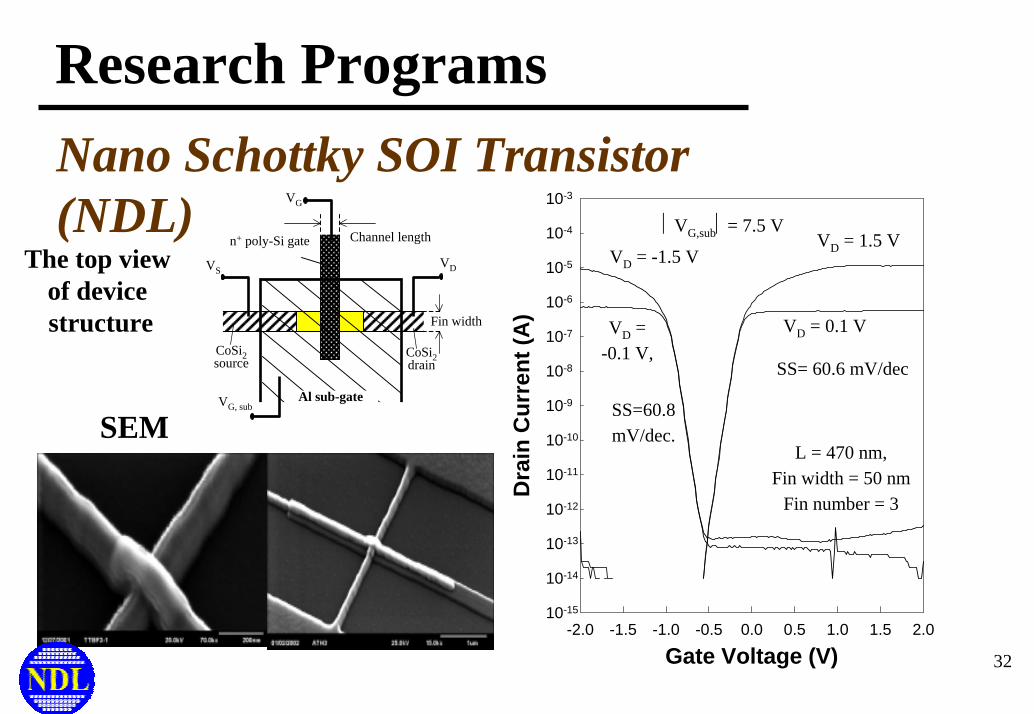
Research Programs
Gate Voltage (V)-2.0 -1.5 -1.0 -0.5 0.0 0.5 1.0 1.5 2.0
Dra
in C
urre
nt (A
)
10-15
10-14
10-13
10-12
10-11
10-10
10-9
10-8
10-7
10-6
10-5
10-4
10-3
SS= 60.6 mV/dec
SS=60.8 mV/dec.
VG,sub= 7.5 V
VD = 0.1 V VD = -0.1 V,
L = 470 nm, Fin width = 50 nm
Fin number = 3
VD = 1.5 V VD = -1.5 V
Nano Schottky SOI Transistor (NDL)
Fin width
Channel length
VS
VG
VG, subAl sub-gate
n+ poly-Si gate
CoSi2source
CoSi2drain
VD
SEM
The top view of device structure

33
(Tri-Gate) FinFET(Intel, VLSI’ 03)
• Tri-gate shows reduced SCE than double gate
• Production after 2007

34
Non-SOI FinFET(Samsung, Toshiba, VLSI’ 03)
Body-tied FinFET (Samsung)
• Reduced cost of SOI wafer • Used for Logic/ DRAM integration

35
Outlines
• Review of the device development• Strategy of nano device development• New device technology and barrier

36
Challenges of Nano Silicon Technology
• Large leakage• Threshold Voltage control• Power dissipation • Cost

37
Control of Leakage
gate
Drain Source
(spacer)
Junction leakagePunch through
Gate leakage
UTB SOI
Scaled down
Direct tunneling from Source to drain
• Near term:reduce gate leakage • Long term:reduce direct tunneling between S/D

38
Power Consumption from Leakage(ISSCC’03)
Leakage
operating
VDD
VTH
2
1
0 2016201220082004
1.5
1
0.75
0.25
0.5
Per transistor
(µW)
Year
V
T = 100 oC1000
100
10
1
0.1
0.01
0.001201020001990198019701960
Year
Power C
onsumption (W
)
Operating power
Leakage power
Intel CPU
Leakage becomes the issue of power consumption !!

39
Parameters fluctuation EffectFrom structure
Line width, doping level, gate oxide thickness
Electrical parameters fluctuation
VTH, ID, Cox, R
Higher fluctuation
Causes:- Failure of circuits- Lost of memory
Good Bad

40
Processes Fluctuation Gate length
Film thickness
UTB SOI
SiO2
SiO2
Poly-Si Gate
Doping level

41
Ultimate Nano MOSFETs(Y. Taur, in short course program of IEDM’01)
G
G
DS
10 nm
Self-aligned metalgates with tunable work functions for threshold control
4 nm thick undoped Si
High-k dielectricwith EOT = 0.5 nm
Tapered source-drain fan-out for reduction of electrical and thermal resistance without high overlap capacitance
(ITRS’2001, 2016, 25 nm-node, physical gate length for MPU: 9 nm) For high-speed IC ( after 2016)

42
New Nano Device Technology
Molecule DevicesSingle electron transistor (SET)Carbon Nanotube
(CNT) Post Si CMOS?Targets: - Cheaper- Less power- High performance DNA ICSpintronics

43
Carbon Nanotube Inter- and IntramolecularLogic Gates (IBM, Nano Lett., 2001)
• CNT exhibits CMOS operation capability
• Barrier: positioning, control of CNT

44
A Dual-Gate-Controlled Single-Electron Transistor using Self-Aligned Polysilicon Sidewall Spacer Gates
on Silicon-on-Insulator NanowireS. F. Hu, Y. C. Wu, C. L. Sung, C. Y. Chang and T. Y. Huang
IEEE Transaction on Nano Technology 2003
ABSTRACTA dual-gate-controlled single-electron transistor was fabricated by using self-aligned polysiliconsidewall spacer gates on a silicon-on-insulatornanowire. The quantum dot formed by the electric field effect of the dual-gate structure was miniaturized to smaller than the state-of-the-art feature size, through a combination of electron beam lithography, oxidation and polysilicon sidewall spacer gate formation processes. The device shows typical MOSFET I-V characteristics at room temperature. However, the Coulomb gap and Coulomb oscillations are clearly observed at 4 K.

45
Requirements of Post Si MOSFET• Size <10 nm
• CMOS operating mode
• High power transfer efficiency Energy efficiency
• High speed
• Room temperature operation P
• Long life time at elevated temperature
• CMOS process compatible
• Stable/ reliable/ reproducible and, Performance

46
Conclusions
• Advanced technology makes IC as the largestindustry
•New ear of 100 nm mass production in 2003•Need new materials/processes/device•The smallest CMOS (L = 9 ~ 10 nm) will be usedfor high speed IC in 2016