Embed Size (px)
Citation preview

2014/7/31
1
Jiing-Yih Lai
Mechanical Engineering Dept.
National Central University
Outline
Structure of the project
Background, project objective and proposed structure
Specific technologies involved in this project
Current simulation and experimental results
Conclusion
2014/7/31
2
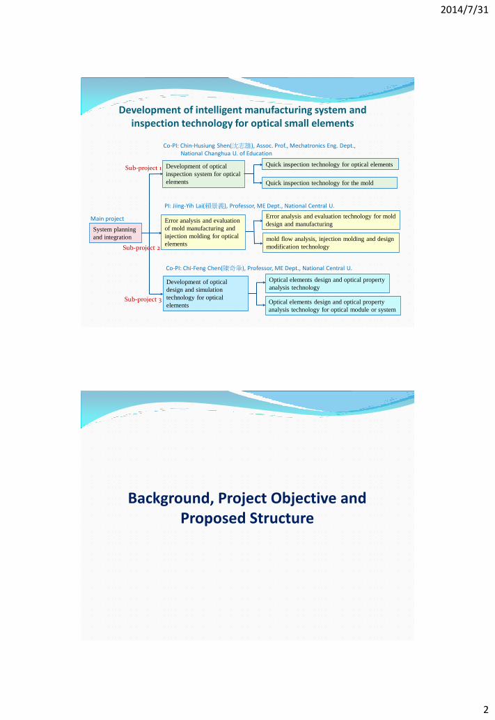
Development of intelligent manufacturing system and inspection technology for optical small elements
Error analysis and evaluation
of mold manufacturing and
injection molding for optical
elements
Development of optical
design and simulation
technology for optical
elements
Development of optical
inspection system for optical
elements
Quick inspection technology for optical elements
Quick inspection technology for the mold
Error analysis and evaluation technology for mold
design and manufacturing
mold flow analysis, injection molding and design
modification technology
Optical elements design and optical property
analysis technology
Optical elements design and optical property
analysis technology for optical module or system
System planning
and integration
Main project
PI: Jiing-Yih Lai(賴景義), Professor, ME Dept., National Central U.
Co-PI: Chi-Feng Chen(陳奇夆), Professor, ME Dept., National Central U.
Co-PI: Chin-Husiung Shen(沈志雄), Assoc. Prof., Mechatronics Eng. Dept., National Changhua U. of Education
Sub-project 1
Sub-project 2
Sub-project 3
Background, Project Objective and Proposed Structure

2014/7/31
3
Problems on the Development of Optical Elements
In injection molding of optical elements, possible reasons for a part failed to reach the required accuracy are as follows:
Improper design
Manufacturing inaccuracy
Inspection uncertainty
Typical manufacturing process of plastic optical elements
CAD Model of
Optical Design
Mold Design &
Manufacturing
Injection
Molding
Part Inspection
Questions frequently occurred Difficult to analyze the reasons causing the problem
Mold design? Mold manufacturing? Injection process?
Difficult to evaluate the surface geometry and material behavior
Specific dimensional measurement only.
If mold flow analysis and optical simulation are included, how accurate they are?
2014/7/31
4
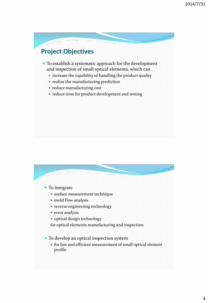
Project Objectives
To establish a systematic approach for the development and inspection of small optical elements, which can
increase the capability of handling the product quality
realize the manufacturing prediction
reduce manufacturing cost
reduce time for product development and testing
To integrate
surface measurement technique
mold flow analysis
reverse engineering technology
error analysis
optical design technology
for optical elements manufacturing and inspection
To develop an optical inspection system
for fast and efficient measurement of small optical element profile
2014/7/31
5
CAD Model
of the Lens
Mold Design,
Manufacturing
And Injection
Molding
Part
STL Meshes
Mole Flow
Analysis
Simulated Part
(STL model)
CAD Model
Reverse Engineering
& Error Analysis
Optical
Measurement
Illuminance and
profile analysis
(Experiment)
Illuminance analysis
(simulated)
Lens Design
and Simulation
Illuminance
analysis
Items analyzed:
1. Surface error analysis
2. Optical illuminance analysis
3. Optical profile inspection
The Proposed Structure
Lens design and simulation is implemented to aide the CAD model design of optical lens
Mold flow analysis is implemented to aide the mold
design and injection manufacturing process
Some more processes are added for the inspection purpose Optical measurement: to analyze the performance of the
injection part, including illuminance and surface profile inspection
Reverse engineering: to reconstruct the CAD model from the scan data of the part
Error analysis: to analyze surface errors among different kinds of data and CAD models

2014/7/31
6
Specific Questions Addressed
How accurate is the injection part?
How accurate is the mold manufacturing?
How accurate is the mold flow analysis?
Optical performance
Combine optical simulation and mold flow analysis for better design of the injection part
Employ optical measurement for quality verification of the injection part
Specific Technologies Involved in this Project
1. Lens Design and Simulation 2. Reverse Engineering 3. Error Analysis 4. Mold Flow Analysis 5. Development of Optical Inspection System

2014/7/31
7
1. Lens Design and Simulation
Motivation:
In LED display, the thickness of backlight module is limited in order to reduce the thickness of the overall product.
The reduction in the thickness may cause a bright spot, and hence result in uneven light emit.
Objectives:
To resolve the hot spot problem for direct type backlight module.
With appropriate lens design, the thickness of backlight module <3 cm.
With a 2 mm diffusion plate, allows evenness of the light>80%
Hot spot LED package and arrangement
Use side emitting lens as an example
0
200
400
600
0 5 10 15 20 25 30 35
Use slope structure to reflect the light from the center to both sides
Original distribution of light intensity
Design objective: reduce light intensity to 50% of the peak value for the region
within 20o from the center point
OSRAM Side-emitting Lens
Lens Design Concept
2014/7/31
8
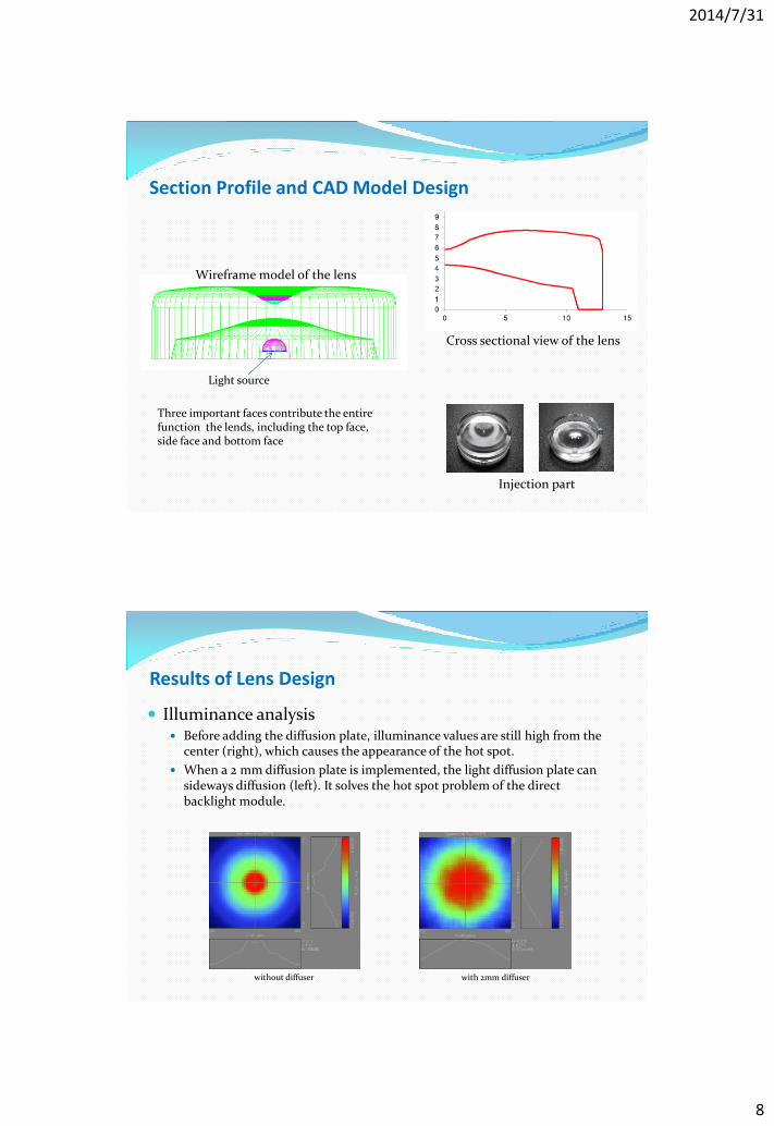
Section Profile and CAD Model Design
Cross sectional view of the lens
Injection part
Light source
Three important faces contribute the entire function the lends, including the top face, side face and bottom face
Wireframe model of the lens
Illuminance analysis Before adding the diffusion plate, illuminance values are still high from the
center (right), which causes the appearance of the hot spot.
When a 2 mm diffusion plate is implemented, the light diffusion plate can sideways diffusion (left). It solves the hot spot problem of the direct backlight module.
with 2mm diffuser
Results of Lens Design
without diffuser

2014/7/31
9
Luminous intensity analysis Reduce luminous intensity of the light of the center within ± 20° to the
peak of 50%.
a small central angle of ± 40° of the light energy is much lower than the exit angle of 50° ~ 70°. Approximately ± 65 ° angle of the light intensity is the strongest.
add diffuser plate is able to meet Lambertion.
Light intensity distribution(without diffuser plate) Light intensity distribution(with 2mm diffuser plate)
Part Optical
Scanning
CAD construction
•Dimensional evaluation
•Surface construction
Modification
•Geometry and surface
•2D drawing
2. Reverse Engineering
Apply optical scanning device to acquire the surface points of the part, physical model, or prototype
Employ the best fit technology to obtain the best surface model from the surface points.
The surface quality should be seriously considered
2014/7/31
10
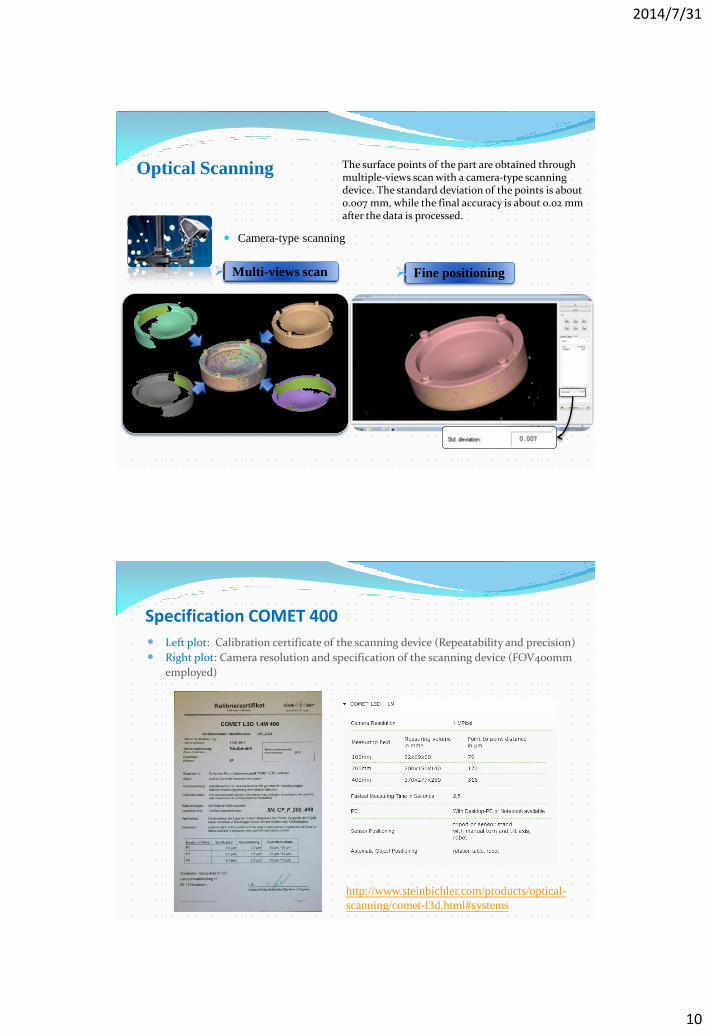
Optical Scanning
Camera-type scanning
Multi-views scan Fine positioning
The surface points of the part are obtained through multiple-views scan with a camera-type scanning device. The standard deviation of the points is about 0.007 mm, while the final accuracy is about 0.02 mm after the data is processed.
Specification COMET 400
http://www.steinbichler.com/products/optical-
scanning/comet-l3d.html#systems
Left plot: Calibration certificate of the scanning device (Repeatability and precision)
Right plot: Camera resolution and specification of the scanning device (FOV400mm
employed)
2014/7/31
11
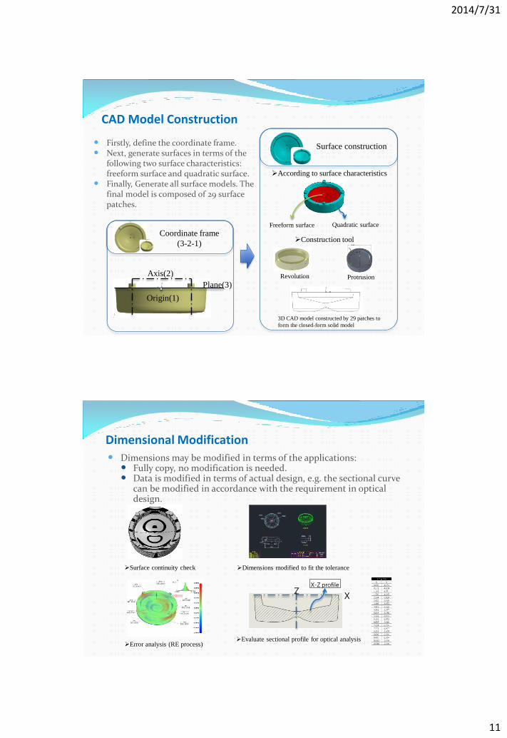
CAD Model Construction
Coordinate frame
(3-2-1)
Plane(3)
Axis(2)
Origin(1)
Surface construction
Quadratic surface Freeform surface
According to surface characteristics
3D CAD model constructed by 29 patches to
form the closed-form solid model
Construction tool
Revolution
Firstly, define the coordinate frame. Next, generate surfaces in terms of the
following two surface characteristics: freeform surface and quadratic surface.
Finally, Generate all surface models. The final model is composed of 29 surface patches.
Protrusion
Dimensional Modification
Surface continuity check
Error analysis (RE process)
Dimensions modified to fit the tolerance
Evaluate sectional profile for optical analysis
Z X
X-Z profile
Dimensions may be modified in terms of the applications: Fully copy, no modification is needed. Data is modified in terms of actual design, e.g. the sectional curve
can be modified in accordance with the requirement in optical design.

2014/7/31
12
3. Error Analysis To analyze the difference between two object surfaces.
Several kinds of error analysis situations: point-to-points, points-to-CAD model, points-to-STL meshes, etc.
Example: Mold flow analysis (STL meshes) vs. Original CAD model (*.igs file)
STL meshes (Mold flow analysis)
Original CAD model
Error distribution
Points-to-CAD Error Analysis
Closest point searching concept Convert the CAD model into triangular
meshes
Meshes subdivision
Closest point searching
Iteration to find real closest point
•Convert all surface models into triangular meshes, including un-trimmed and trimmed surfaces. The number of meshes is adjusted in terms of the size of each surface
Convert CAD to meshes
•Evaluate the corresponding cell of a data point. Find a set of meshes which lie within the cells. Find the mesh which is closest to the data point.
Closest point computation
Iteration for real closest point
•Based on the bounding box of the entire set of meshes, divide the volume into cells. Record the cells on the boundary of the object surface.
Meshes subdivision
•Use Jacobian Inversion method to evaluate the point which is closest to the data point. An iteration algorithm must be implemented to find the closest point.

2014/7/31
13
4. Mold Flow Analysis
Modex3D mold flow analysis process
Parameters to be determined by users
Output of mold flow analysis
Initial simulation: Original side emitter
New mold design & simulation results
Cave design: one cave vs. four caves
Modex3D Mold Flow Analysis Process Step1:Design Model
Meet the needs of the model
Step2:Input Model
Build solid mesh of the optical lens design. Different ways of building solid mesh can affect the simulation results.
Step3:Simulating
Get some simulation results in different stages: Filling, Packing, Cooling, and Warpage.
Step4:Results
Determine whether the result is a good design
2014/7/31
14
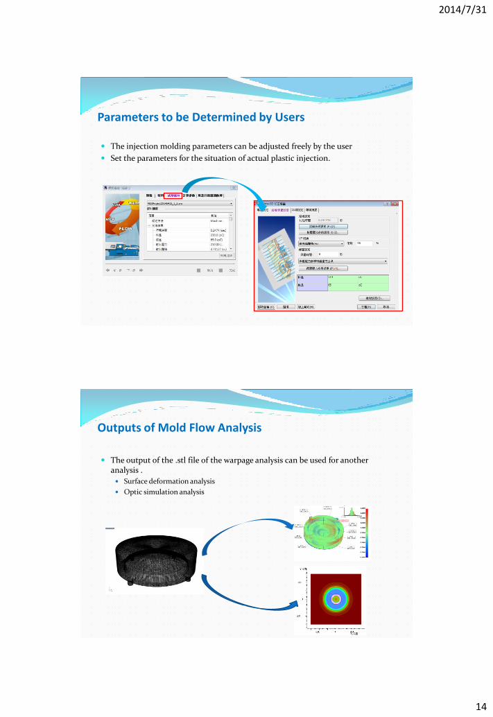
Parameters to be Determined by Users
The injection molding parameters can be adjusted freely by the user
Set the parameters for the situation of actual plastic injection.
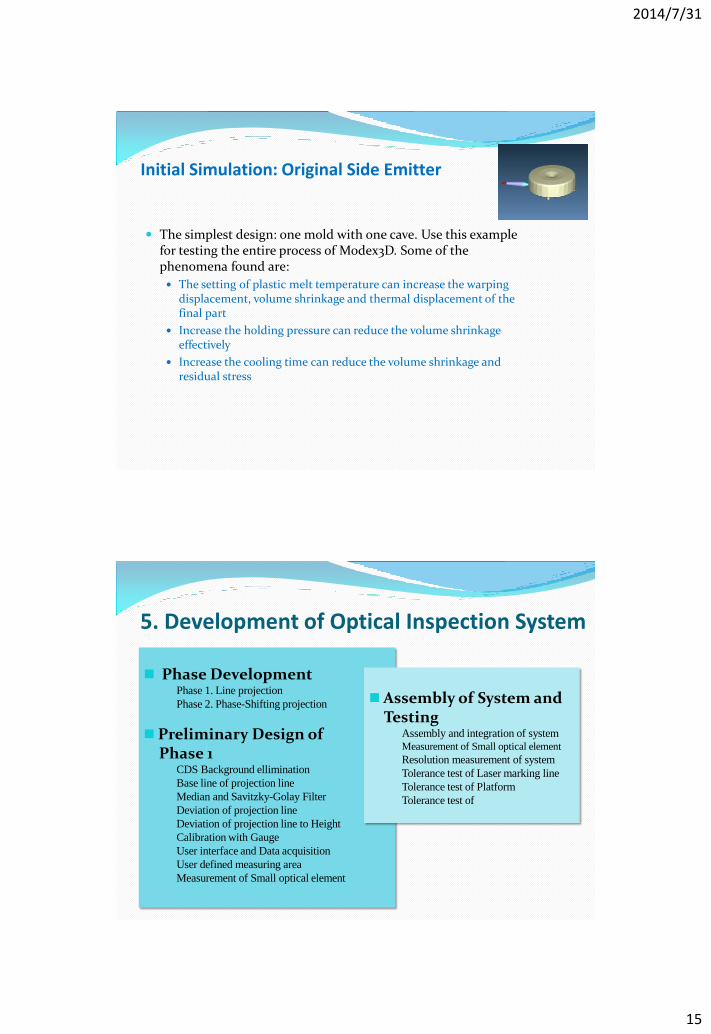
Outputs of Mold Flow Analysis
The output of the .stl file of the warpage analysis can be used for another analysis .
Surface deformation analysis
Optic simulation analysis
2014/7/31
15
Initial Simulation: Original Side Emitter
The simplest design: one mold with one cave. Use this example for testing the entire process of Modex3D. Some of the phenomena found are:
The setting of plastic melt temperature can increase the warping displacement, volume shrinkage and thermal displacement of the final part
Increase the holding pressure can reduce the volume shrinkage effectively
Increase the cooling time can reduce the volume shrinkage and residual stress
5. Development of Optical Inspection System
Phase Development Phase 1. Line projection
Phase 2. Phase-Shifting projection
Preliminary Design of Phase 1
CDS Background ellimination
Base line of projection line
Median and Savitzky-Golay Filter
Deviation of projection line
Deviation of projection line to Height
Calibration with Gauge
User interface and Data acquisition
User defined measuring area
Measurement of Small optical element
Assembly of System and Testing
Assembly and integration of system
Measurement of Small optical element
Resolution measurement of system
Tolerance test of Laser marking line
Tolerance test of Platform
Tolerance test of
2014/7/31
16
Phase 1: Design of Line Projection System
Using a laser projection marker
with 0.38 mm width, it is
projected with 450 inclination
angle. The laser module is
installed at 120 mm height and
the telecentric lens module with
is positioned at 65 mm from the
measurement platform。
High resolution 744×480
RGB32bit CMOS image
module with USB interface
雷射
CCD
遠心鏡組
基準平台
待測物
45゚
65
mm
120 mm
12
0 m
m
Phase 2: Phase-Shifting projection
2014/7/31
17
Preliminary Design of Phase-Shifting Projection
Optical Design of Phase-Shifting projection
System Design and Algorithm • DMD Phase Modulation
• Algorithm of Four Phase-
Shifting with CDS
Design and Prototype of Line projection
遠心鏡組
投射光源
待測組件
投射光源
待測組件
2014/7/31
18
Lens Measurement with Prototype of Line Projection
Design of User Interface
影像顯示區
焊點厚度記錄區
控制區
測量結果顯示區
2014/7/31
19
Control Panel and System Parameters Setup
影像雜訊濾波更名為影像強化,增加不同的強化段數
光源調節段數減少 新增記錄檔名與預設檔名
更名為自動基準面選定
Background Elimination : Double sampling images with Laser projection
Image
Capture
Brightness control
Average
After Background
Cancellation
2014/7/31
20
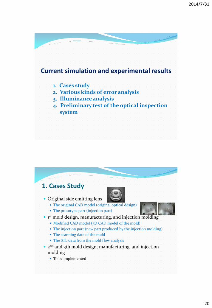
Current simulation and experimental results
1. Cases study 2. Various kinds of error analysis 3. Illuminance analysis 4. Preliminary test of the optical inspection system
1. Cases Study
Original side emitting lens The original CAD model (original optical design)
The prototype part (injection part)
1st mold design, manufacturing, and injection molding Modified CAD model (3D CAD model of the mold)
The injection part (new part produced by the injection molding)
The scanning data of the mold
The STL data from the mold flow analysis
2nd and 3th mold design, manufacturing, and injection molding To be implemented
2014/7/31
21
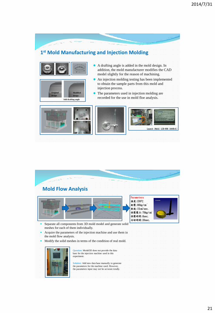
1st Mold Manufacturing and Injection Molding
Original
design
Modified
design
Add drafting angle
A drafting angle is added in the mold design. In
addition, the mold manufacturer modifies the CAD
model slightly for the reason of machining.
An injection molding testing has been implemented
to obtain the sample parts from this mold and
injection process.
The parameters used in injection molding are
recorded for the use in mold floe analysis.
Launch (隆泉) LCH-80B (肘節式)
Mold Flow Analysis
Separate all components from 3D mold model and generate solid
meshes for each of them individually.
Acquire the parameters of the injection machine and use them in
the mold flow analysis.
Modify the solid meshes in terms of the condition of real mold.
Parameters
溫度:230℃
射壓:80㎏/㎝
射速:15㎝/sec.
保壓壓力:70㎏/㎝
保壓時間:8sec.
冷卻時間:20sec.
2
2
3
Question: Model3D does not provide the data
base for the injection machine used in this
experiment.
Solution: Add new data base manually to generate
the parameters for the machine used. However,
the parameters input may not be accurate totally.
2014/7/31
22
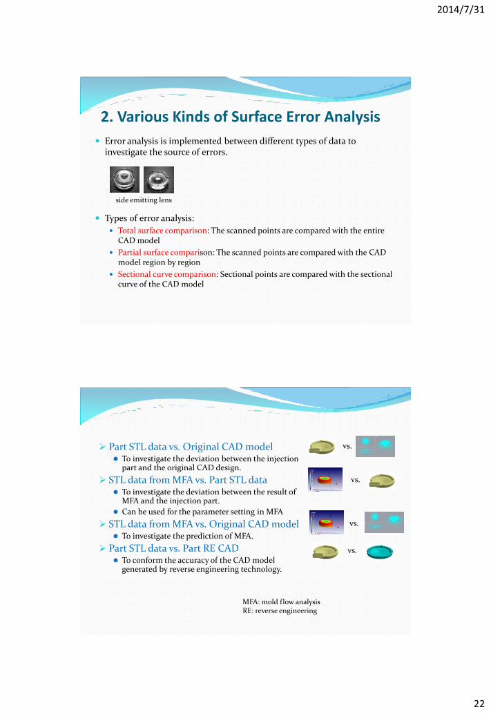
2. Various Kinds of Surface Error Analysis
Error analysis is implemented between different types of data to investigate the source of errors.
Types of error analysis:
Total surface comparison: The scanned points are compared with the entire CAD model
Partial surface comparison: The scanned points are compared with the CAD model region by region
Sectional curve comparison: Sectional points are compared with the sectional curve of the CAD model
side emitting lens
vs.
vs.
vs.
vs.
Part STL data vs. Original CAD model To investigate the deviation between the injection
part and the original CAD design.
STL data from MFA vs. Part STL data To investigate the deviation between the result of
MFA and the injection part.
Can be used for the parameter setting in MFA
STL data from MFA vs. Original CAD model To investigate the prediction of MFA.
Part STL data vs. Part RE CAD To conform the accuracy of the CAD model
generated by reverse engineering technology.
MFA: mold flow analysis RE: reverse engineering
2014/7/31
23
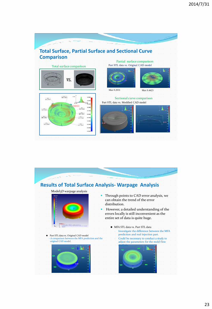
Total Surface, Partial Surface and Sectional Curve Comparison
VS.
Part STL data vs. Original CAD model
Max 0.2031 Max 0.4423
Part STL data vs. Modified CAD model
Total surface comparison
Partial surface comparison
Sectional curve comparison
Results of Total Surface Analysis- Warpage Analysis
Part STL data vs. Original CAD model - A comparison between the MFA prediction and the original CAD model.
MFA STL data vs. Part STL data
- Investigate the difference between the MFA prediction and real injection part.
- Could be necessary to conduct a study to adjust the parameters for the mold flow analysis.
Model3D warpage analysis
Through points to CAD error analysis, we can obtain the trend of the error distribution.
However, a detailed understanding of the errors locally is still inconvenient as the entire set of data is quite huge.
2014/7/31
24
MFA STL data vs. Part STL data
Part STL data vs. Part RE CAD model Part STL data vs. Original CAD model
Part STL data vs. Original CAD model
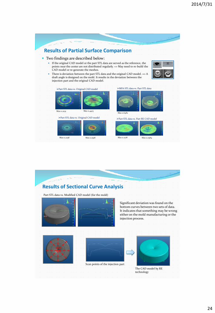
Results of Partial Surface Comparison
Max 0.2031 Max 0.4423 Max 0.6482
Max 0.2258 Max 0.0918 Max 0.1278 Max 0.0584
Two findings are described below: If the original CAD model or the part STL data are served as the reference, the
points near the center are not distributed regularly. => May need to re-build the CAD model or re-generate the meshes.
There is deviation between the part STL data and the original CAD model. => A draft angle is designed on the mold. It results in the deviation between the injection part and the original CAD model.
Results of Sectional Curve Analysis
Part STL data vs. Modified CAD model (for the mold)
The CAD model by RE technology
Scan points of the injection part
Significant deviation was found on the bottom curves between two sets of data. It indicates that something may be wrong either on the mold manufacturing or the injection process.

2014/7/31
25
Part STL data vs. Modified CAD model
Plane fitting error, Max: 0.0170, RMS: 0.0054
Registration verification
Preliminary Conclusion
Item Mold flow analysis vs. modified CAD model Part STL data vs. Modified CAD model
Max error 0.1247 mm (Location: side face) 0.1604 mm (Location): lower face)
Rms error 0.0501 mm 0.0470 mm
Upper face Error range: approximately 0.01-0.03 mm Error range: approximately 0.01-0.05 mm
Lower face Error range: approximately 0.01-0.05 mm Error range: approximately 0.01-0.16 mm
Side face Error range: approximately 0.08-0.12 mm Error range: approximately 0.01-0.02 mm
Based on the left result, the side face has more error as an amount of shrinkage is added on the CAD model of the mold.
Based on the right result, the lower face has more error than the other two area, which might be due to the manufacturing error on the mold in this area.
Conclusion: Upper faces on both results are quite similar. There might exist some errors between the CAD model of the mold and real mold. A scanning of the mold surface is necessary to verify such an observation.

2014/7/31
26
Shrinkage Design for the Mold
1.51273 mm 1.5052 mm
CAD model of the part CAD model of the mold
縮放中心
The original CAD model is expanded uniformly along three axes.
The expansion ratio is 0.5%, namely the CAD model is expanded 1.004 along each axis.
The accuracy of the CNC machine: +/- 0.1 mm
Need to inspect the mold in order to verify its accuracy.
3. Illuminance Analysis
Illuminance simulation Theoretical illuminance due to optical design
Illuminance measurement Measurement of real parts
Illuminance analysis due to MFA Simulated illuminance from mold flow analysis
Comparison of three kinds of analysis
<2>透鏡打樣實際量測結果
<1>原始光學設計檔案。 微型光學元件製造技術與檢測技術開發
<3>3D掃描透鏡後CAD檔案
模擬數據和實驗量測數據進行比對
2014/7/31
27
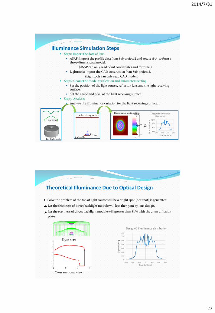
Illuminance Simulation Steps Step1: Import the data of lens
ASAP: Import the profile data from Sub-project 2 and rotate 1800 to form a three-dimensional model.
(ASAP can only read point coordinates and formula.)
Lighttools: Import the CAD construction from Sub-project 2.
(Lighttools can only read CAD model.)
Step2: Geometric model verification and Parameters setting
Set the position of the light source, reflector, lens and the light receiving surface.
Set the shape and pixel of the light receiving surface.
Step3: Analysis
Analyze the illuminance variation for the light receiving surface.
For ASAP
For Lighttools
Receiving surface
Reflector Lens
&
Illuminance distribution
-100
400
900
1400
-300 -100 100 300
Illum
inan
ce(lx)
Location(mm)
Designed illuminance distribution
1. Solve the problem of the top of light source will be a bright spot (hot spot) is generated.
2. Let the thickness of direct backlight module will less then 3cm by lens design.
3. Let the evenness of direct backlight module will greater than 80% with the 2mm diffusion
plate.
0
200
400
600
800
1000
1200
1400
-300 -200 -100 0 100 200 300
Illum
inan
ce(lx)
Location(mm)
Designed illuminance distribution
Cross sectional view
Front view
Theoretical Illuminance Due to Optical Design

2014/7/31
28
Measured illuminance by using the light meter.
Measured illuminance distribution:
The result is shown that the illuminance distribution is not
symmetrical.
Light meter
Lens
Reflector
85mm
gate
Measurement of the environment
Movement direction of light meter
0
100
200
300
400
500
600
700
-40 -20 0 20 40
Illum
inan
ce(lx)
Location(mm)
Measured illuminance distribution
Measurement of Real Parts
Measured direction
Simulated Illuminance from Mold Flow Analysis (Mold Flow Illuminance )
We can’t accurately know the illumance distribution from each surface, so we figure out the method that analysis illuminance for diffirent dimension.
We can get the lens profile for diffirent dimension by using RevCAD.(Lens profile is provided by sub-project 2.)
0
200
400
600
800
1000
1200
1400
1600
1800
-300 -200 -100 0 100 200 300
Illum
inan
ce(lx)
Locatiom(mm)
Mold flow illuminance distribution
2014/7/31
29
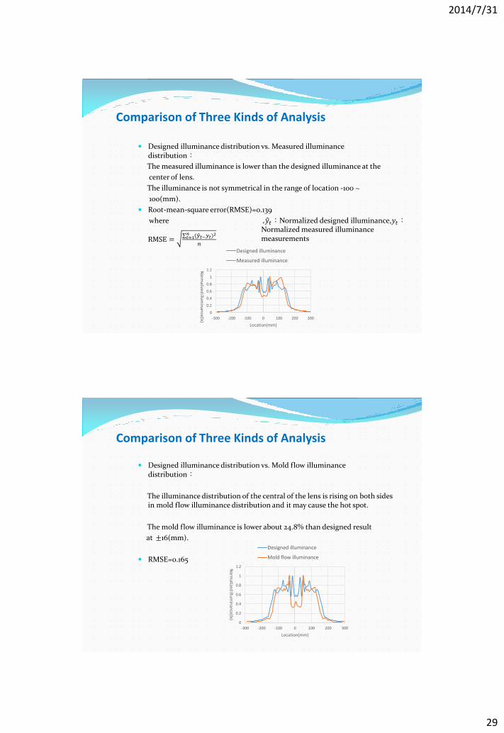
Comparison of Three Kinds of Analysis
Designed illuminance distribution vs. Measured illuminance distribution:
The measured illuminance is lower than the designed illuminance at the
center of lens.
The illuminance is not symmetrical in the range of location -100 ~
100(mm).
Root-mean-square error(RMSE)=0.139
where
RMSE = (𝑦 𝑡−𝑦𝑡)
2𝑛𝑡=1
𝑛
0
0.2
0.4
0.6
0.8
1
1.2
-300 -200 -100 0 100 200 300
No
rmalized
illum
inan
ce(lx)
Location(mm)
Designed illuminance
Measured illuminance
,𝑦 𝑡:Normalized designed illuminance,𝑦𝑡: Normalized measured illuminance measurements
Comparison of Three Kinds of Analysis
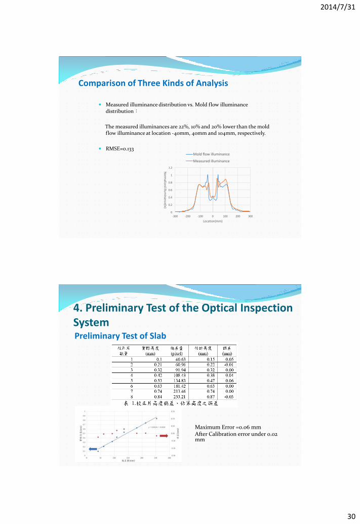
Designed illuminance distribution vs. Mold flow illuminance distribution:
The illuminance distribution of the central of the lens is rising on both sides in mold flow illuminance distribution and it may cause the hot spot.
The mold flow illuminance is lower about 24.8% than designed result
at ±16(mm).
RMSE=0.165
0
0.2
0.4
0.6
0.8
1
1.2
-300 -200 -100 0 100 200 300
No
rmalized
illum
inan
ce(lx)
Location(mm)
Designed illuminance
Mold flow illuminance
2014/7/31
30
Comparison of Three Kinds of Analysis
0
0.2
0.4
0.6
0.8
1
1.2
-300 -200 -100 0 100 200 300
No
rmalized
illum
inan
ce(lx)
Location(mm)
Mold flow illuminance
Measured illuminance
Measured illuminance distribution vs. Mold flow illuminance distribution:
The measured illuminances are 22%, 10% and 20% lower than the mold flow illuminance at location -40mm, 40mm and 104mm, respectively.
RMSE=0.133
Preliminary Test of Slab
Maximum Error =0.06 mm After Calibration error under 0.02 mm
4. Preliminary Test of the Optical Inspection System
2014/7/31
31
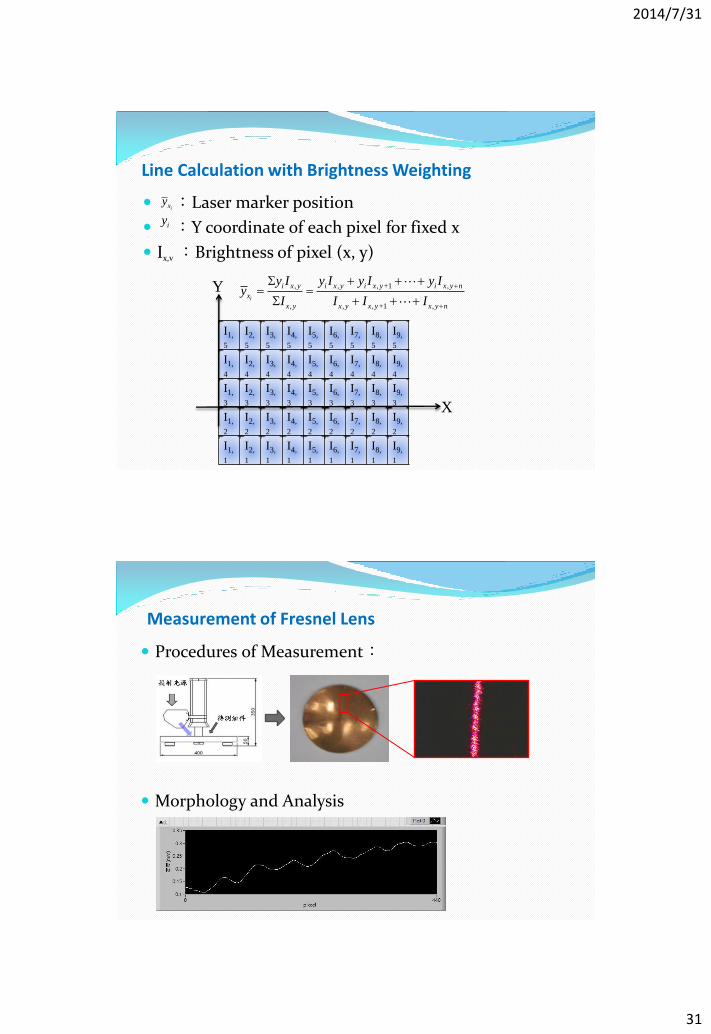
Line Calculation with Brightness Weighting
I1,
5
I2,
5
I3,
5
I4,
5
I5,
5
I6,
5
I7,
5
I8,
5
I9,
5
I1,
4
I2,
4
I3,
4
I4,
4
I5,
4
I6,
4
I7,
4
I8,
4
I9,
4
I1,
3
I2,
3
I3,
3
I4,
3
I5,
3
I6,
3
I7,
3
I8,
3
I9,
3
I1,
2
I2,
2
I3,
2
I4,
2
I5,
2
I6,
2
I7,
2
I8,
2
I9,
2
I1,
1
I2,
1
I3,
1
I4,
1
I5,
1
I6,
1
I7,
1
I8,
1
I9,
1
X
Y , , , +1 ,
, , , +1 ,i
i x y i x y i x y i x y n
x
x y x y x y x y n
y I y I y I y Iy
I I I I
:Laser marker position
:Y coordinate of each pixel for fixed x
Ix,v :Brightness of pixel (x, y)
ixy
iy
Measurement of Fresnel Lens
Procedures of Measurement:
Morphology and Analysis
2014/7/31
32
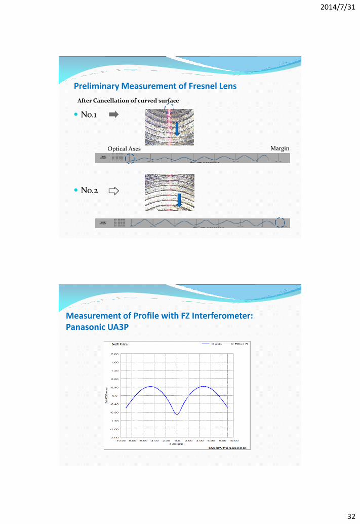
Preliminary Measurement of Fresnel Lens
No.1
No.2
Optical Axes Margin
After Cancellation of curved surface
Measurement of Profile with FZ Interferometer: Panasonic UA3P
2014/7/31
33
Conclusions
A systematic approach has been developed and tested for the accuracy analysis of small optical elements in terms of mold manufacturing and injection molding.
Combine mold flow analysis and optical simulation during the development of optical elements in order to improve the quality of the injection parts.
An optical inspection system has been developed for the purpose of online inspection. An initial system, including hardware and software, has been setup and tested. Preliminary test results are available.