Embed Size (px)
Citation preview

ARL-TR-7349 ● JULY 2015
US Army Research Laboratory
Development of a Multi-layer Anti-reflective Coating for Gallium Arsenide/Aluminum Gallium Arsenide Solar Cells
by Kimberley A Olver Approved for public release; distribution unlimited.

NOTICES
Disclaimers The findings in this report are not to be construed as an official Department of the Army position unless so designated by other authorized documents.
Citation of manufacturer’s or trade names does not constitute an official endorsement or approval of the use thereof.
Destroy this report when it is no longer needed. Do not return it to the originator.

ARL-TR-7349 ● JULY 2015
US Army Research Laboratory
Development of a Multi-layer Anti-reflective Coating for Gallium Arsenide/Aluminum Gallium Arsenide Solar Cells
by Kimberley A Olver Sensors and Electron Devices Directorate, ARL Approved for public release; distribution unlimited.
FOR OFFICIAL USE ONLY (delete if not FOUO)
ii
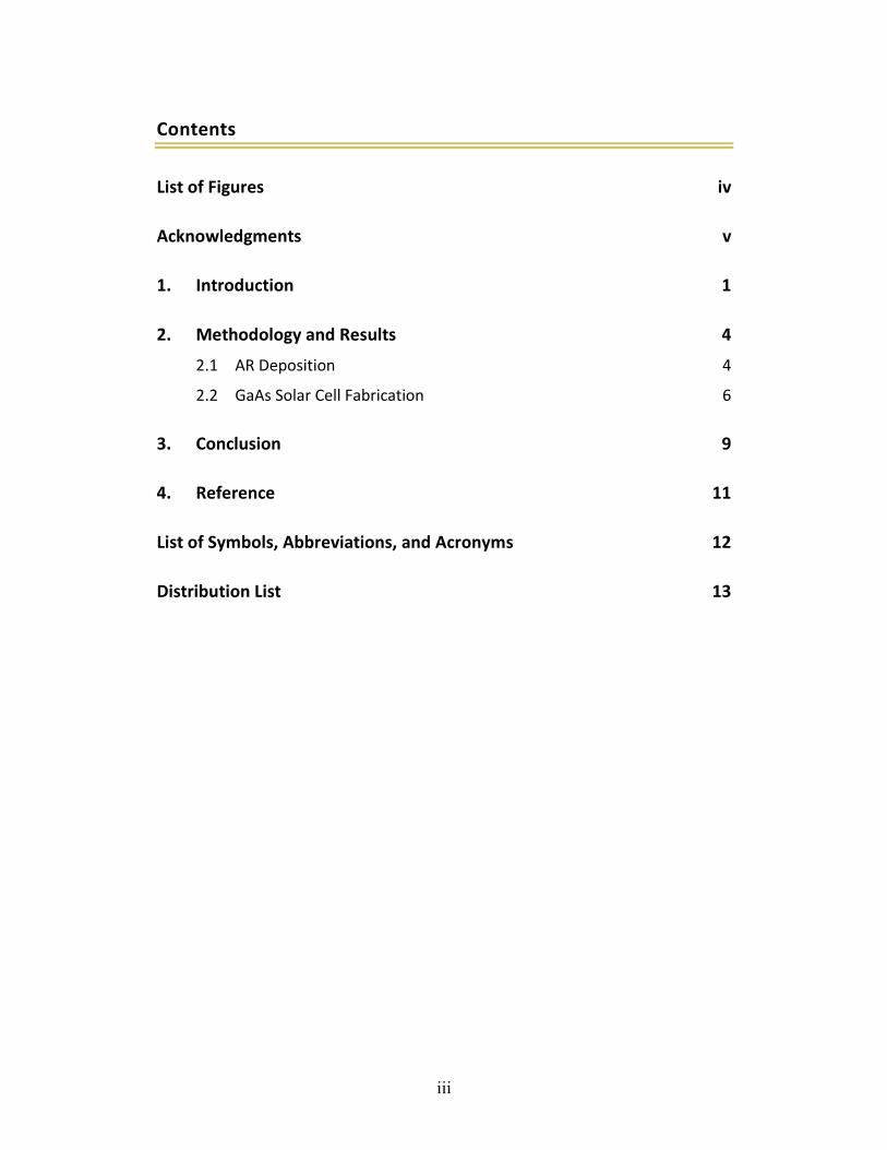
REPORT DOCUMENTATION PAGE Form Approved OMB No. 0704-0188
Public reporting burden for this collection of information is estimated to average 1 hour per response, including the time for reviewing instructions, searching existing data sources, gathering and maintaining the data needed, and completing and reviewing the collection information. Send comments regarding this burden estimate or any other aspect of this collection of information, including suggestions for reducing the burden, to Department of Defense, Washington Headquarters Services, Directorate for Information Operations and Reports (0704-0188), 1215 Jefferson Davis Highway, Suite 1204, Arlington, VA 22202-4302. Respondents should be aware that notwithstanding any other provision of law, no person shall be subject to any penalty for failing to comply with a collection of information if it does not display a currently valid OMB control number. PLEASE DO NOT RETURN YOUR FORM TO THE ABOVE ADDRESS.
1. REPORT DATE (DD-MM-YYYY)
July 2015 2. REPORT TYPE
Final 3. DATES COVERED (From - To)
4. TITLE AND SUBTITLE
Development of a Multi-layer Anti-reflective Coating for Gallium Arsenide (GaAs)/Aluminum Gallium Arsenide (AlGaAs) Solar Cells
5a. CONTRACT NUMBER
5b. GRANT NUMBER
5c. PROGRAM ELEMENT NUMBER
6. AUTHOR(S)
Kimberley A Olver 5d. PROJECT NUMBER
5e. TASK NUMBER
5f. WORK UNIT NUMBER
7. PERFORMING ORGANIZATION NAME(S) AND ADDRESS(ES)
US Army Research Laboratory ATTN: RDRL-SEE-I 2800 Powder Mill Road Adelphi, MD 20783-1138
8. PERFORMING ORGANIZATION REPORT NUMBER
ARL-TR-7349
9. SPONSORING/MONITORING AGENCY NAME(S) AND ADDRESS(ES)
10. SPONSOR/MONITOR'S ACRONYM(S)
11. SPONSOR/MONITOR'S REPORT NUMBER(S)
12. DISTRIBUTION/AVAILABILITY STATEMENT
Approved for public release; distribution unlimited.
13. SUPPLEMENTARY NOTES
14. ABSTRACT
A process for calculating the true refractive index of an as-deposited dielectric for use as an anti-reflective (AR) coating was established. Yttrium oxide and tantalum oxide were used in the design of multi-layer AR coatings for use with gallium arsenide (GaAs) solar cell devices. These AR coatings were found to greatly reduce the reflective losses from the surface of the GaAs, therefore increasing the external quantum efficiency of the device.
15. SUBJECT TERMS
anti-reflective, gallium arsenide, GaAs solar
16. SECURITY CLASSIFICATION OF: 17. LIMITATION OF ABSTRACT
UU
18. NUMBER OF PAGES
22
19a. NAME OF RESPONSIBLE PERSON
Kimberley A Olver a. REPORT
Unclassified b. ABSTRACT
Unclassified c. THIS PAGE
Unclassified 19b. TELEPHONE NUMBER (Include area code)
301-394-2048 Standard Form 298 (Rev. 8/98) Prescribed by ANSI Std. Z39.18
iii
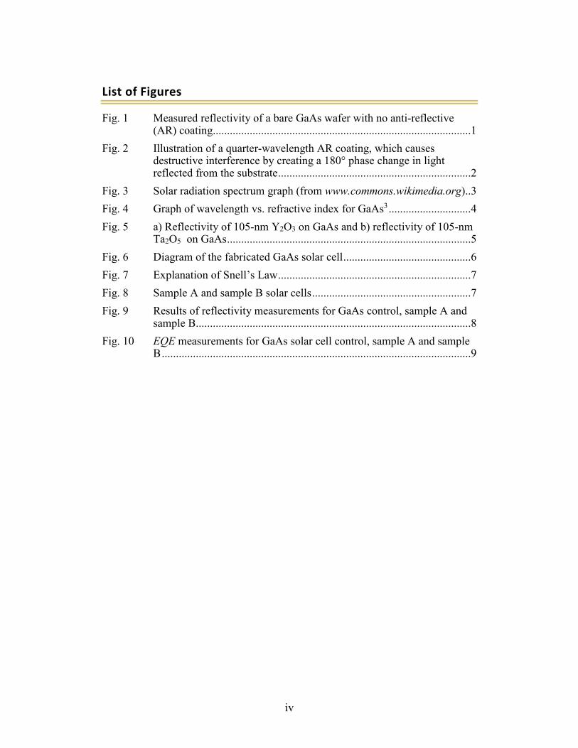
Contents
List of Figures iv
Acknowledgments v
1. Introduction 1
2. Methodology and Results 4
2.1 AR Deposition 4
2.2 GaAs Solar Cell Fabrication 6
3. Conclusion 9
4. Reference 11
List of Symbols, Abbreviations, and Acronyms 12
Distribution List 13
iv
List of Figures
Fig. 1 Measured reflectivity of a bare GaAs wafer with no anti-reflective (AR) coating...........................................................................................1
Fig. 2 Illustration of a quarter-wavelength AR coating, which causes destructive interference by creating a 180° phase change in light reflected from the substrate ....................................................................2
Fig. 3 Solar radiation spectrum graph (from www.commons.wikimedia.org) ..3
Fig. 4 Graph of wavelength vs. refractive index for GaAs3 .............................4
Fig. 5 a) Reflectivity of 105-nm Y2O3 on GaAs and b) reflectivity of 105-nm Ta2O5 on GaAs ......................................................................................5
Fig. 6 Diagram of the fabricated GaAs solar cell .............................................6
Fig. 7 Explanation of Snell’s Law ....................................................................7
Fig. 8 Sample A and sample B solar cells ........................................................7
Fig. 9 Results of reflectivity measurements for GaAs control, sample A and sample B.................................................................................................8
Fig. 10 EQE measurements for GaAs solar cell control, sample A and sample B .............................................................................................................9
v
Acknowledgments
The author would like to acknowledge Mr Fred Towner, formerly of Maxion Technologies, for growing the gallium arsenide wafer from which the test solar cells were made, and Dr Eric DeCuir, Jr, of the US Army Research Laboratory (ARL) for his support in writing this report.
vi
INTENTIONALLY LEFT BLANK.
1
1. Introduction
The Army has been developing new types of photovoltaic (PV) devices – solar cells – for use in its efforts to more efficiently functionalize the Army warfighter. Gallium arsenide (GaAs) solar cells as well as other III-V semiconductors are currently being studied for their advantages over silicon solar cells. Because GaAs is a direct bandgap material, its conversion of light into power is more efficient than silicon. This gives GaAs solar cells the advantage in low-light conditions. Further, with their multi-junction architecture, GaAs solar cells are able to respond to multiple wavelengths of light, also increasing their efficiency.
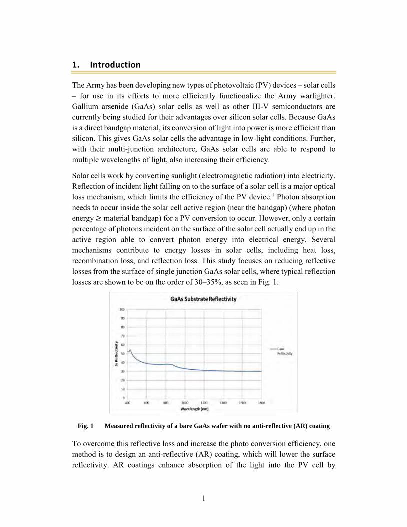
Solar cells work by converting sunlight (electromagnetic radiation) into electricity. Reflection of incident light falling on to the surface of a solar cell is a major optical loss mechanism, which limits the efficiency of the PV device.1 Photon absorption needs to occur inside the solar cell active region (near the bandgap) (where photon energy ≥ material bandgap) for a PV conversion to occur. However, only a certain percentage of photons incident on the surface of the solar cell actually end up in the active region able to convert photon energy into electrical energy. Several mechanisms contribute to energy losses in solar cells, including heat loss, recombination loss, and reflection loss. This study focuses on reducing reflective losses from the surface of single junction GaAs solar cells, where typical reflection losses are shown to be on the order of 30–35%, as seen in Fig. 1.
Fig. 1 Measured reflectivity of a bare GaAs wafer with no anti-reflective (AR) coating
To overcome this reflective loss and increase the photo conversion efficiency, one method is to design an anti-reflective (AR) coating, which will lower the surface reflectivity. AR coatings enhance absorption of the light into the PV cell by

2
decreasing the reflection off of the semiconductor surface. AR coatings work by creating a 2 reflective wave scenario, one from the surface of the coating and the other from the surface of the substrate. The AR coating is designed so that these 2 waves destructively interfere with each other when reflected, cancelling each other out (Fig. 2).
Fig. 2 Illustration of a quarter-wavelength AR coating, which causes destructive interference by creating a 180° phase change in light reflected from the substrate
Typical AR coatings consist of dielectric materials with calculated thicknesses and refractive indices that closely match the optimal refractive index of the solar cell material for a given wavelength. The refractive index (n) of a material is defined as the ratio of the speed of light in a vacuum and the speed of light in a material or
materialinlightofVelocityvacuuminlightofVelocityn = (1)
By lowering the reflectivity of the surface, more light particles (photons) are able to be absorbed, and therefore, generate more photocurrent in the solar cell. As the photon having energy equal to or greater than the bandgap travels into the material, a conversion (photon absorption) occurs. For GaAs, a photon of energy 1.424 eV (or greater) transfers its energy to an electron in the valence band, which enables the electron to overcome the bandgap energy and move into the conduction band, leaving a hole behind in the valence band. This combination is known as an electron-hole pair and is responsible for charge moving through the PV device. These electron-hole pairs are also known as charge carriers. A measure of the photon to electron conversion efficiency in the material is referred to as the quantum efficiency (QE) and is basically the measure of the solar cell’s sensitivity
1λ
λ/4Anti-reflective coating
R1
R2 DestructiveInterference
SubstrateTransmission
Photon (λ)
Reflectance:

3
to light. QE is the ratio of the number of carriers collected by the solar cell to the number of photons of a given energy incident on the solar cell.1 It is the ratio of electrons out versus photons in:
in/secondPhotonsout/secondElectronsQE = (2)
A single layer AR coating reduces reflectance in a narrow wavelength area, however a 2 (or more) layer AR coating of the correct dielectric materials can broaden out the wavelength area where the reflections are at a minimum. Our GaAs solar cells operate in the 400–900 nm spectral range. Because of this broad spectral range, a multilayer AR coating was designed and fabricated to lower the reflectivity in the 600 to 900 nm wavelength range. This wavelength range also aligns with the peak power of the solar spectrum, thus the most power (solar radiation) available to our devices (Fig. 3).
Fig. 3 Solar radiation spectrum graph (from www.commons.wikimedia.org)
Ideally, for an AR coating to create a completely reflective-free interface with the solar cell material, it will have an optimal refractive index matched to the semiconductor material used for the solar cell, in this case, GaAs. In addition to matching the optimal refractive index, a quarter-wavelength coating thickness is chosen to ensure reflected light from the coating surface as well as the reflection from the AR coating/substrate interface are 180° out of phase (see Fig. 2). We calculate the optimal refractive index (n) from the following equation:
nλ/4 = sqrt(nair x nsemi), (3)

4
where nλ/4 is the optimal refractive index of the AR material for a wavelength λ, nair is the refractive index of air (equal to 1), and nsemi is the refractive index of the semiconductor material (Fig. 4). Solving the equation for the optimal refractive index of GaAs at 880 nm (n = 3.6 at 880 nm), the calculated optimal index of refraction of GaAs at 880 nm is 1.89.
Fig. 4 Graph of wavelength vs. refractive index for GaAs3
2. Methodology and Results
Reported refractive indices of several dielectric materials were evaluated, and 2 were chosen as being close to the square root of the refractive index of GaAs at 880 nm, also known as the optimal index for GaAs (1.89). After evaluating several dielectric materials, yttrium oxide (Y2O3) and tantalum pentoxide (Ta2O5) were chosen due to their reported refractive indices at 880 nm being very close to this optimal refractive index. Refractive indices reported in the literature for Y2O3 and Ta2O5 were 1.91 and 2.11, respectfully,3,4 but to find the actual index of the material that would be used, each material was first evaporated onto an individual GaAs wafer and characterized. Reported and actual refractive indices of materials vary due to several factors including material density and deposition processes.
2.1 AR Deposition
The AR depositions were performed on an Evatec BAK 641 electron-beam evaporator with a chamber pressure of 2x10⁻⁶ Torr, and an oxygen (O2) back pressure of 3x10⁻⁴ Torr. The O2 back pressure was used to keep the stoichiometry of the dielectric materials constant while the depositions took place. The deposition

5
rate was 1.3 Å/s for each material. Thicknesses of 105 nm of Y2O3 and 105 nm of Ta2O5 were evaporated onto individual GaAs wafers. Characterization took place using a Perkin Elmer Lambda 950 UV/VIS Spectrophotometer. A measurement of reflectivity (R) versus wavelength was performed on both evaporated films as well as a control sample GaAs substrate (Fig. 5).
Fig. 5 a) Reflectivity of 105-nm Y2O3 on GaAs and b) reflectivity of 105-nm Ta2O5 on GaAs
As the graphs show, a 2.0% minimum reflectance at the 732-nm wavelength for Y2O3, and a 0.2% minimum reflectance at the 870-nm wavelength for Ta2O5 were measured for these deposited films. Using the measured thickness of the 2 coatings, the empirical refractive index at these minima were calculated using the following equation:
d = (λ)/4 × n, (4)
where d is the thickness of the original film (105 nm) and λ is the wavelength of the measured minimum reflection for each dielectric. We calculate the actual index of
Minimum reflectance of 2.0% at 732nm
a)
Minimum reflectance of 0.2% at 870nm nm
b)

6
refraction for our materials as 1.74 for Y2O3, and 2.07 for Ta2O5. These measured refractive indices match quite well with the indices reported in literature, and deviations from the reported indices could be attributed to deposition techniques, which may have produced slight density variations in the film. Using these new refractive indices and the wavelength of interest, the calculations were repeated for the correct thicknesses needed for our AR coatings at the 800-nm wavelength. From these new thickness calculations, 2-layer multilayer structures were designed and deposited onto fabricated GaAs solar cells.
2.2 GaAs Solar Cell Fabrication
GaAs solar cells were fabricated using standard photolithographic techniques. A wafer was grown using molecular beam epitaxial (MBE) technology. The simple device design consisted of a single p-n junction of GaAs/aluminum gallium arsenide (AlGaAs) structure with a p-type top contact, an absorbing layer of AlGaAs, and an n-type bottom contact. Three solar cell devices were fabricated from this wafer. First, individual 5x5 mm2 device mesas were etched into the substrate. Next, a blanket contact of gold/tin/gold (Au/Sn/Au) was e-beam vacuum evaporated onto the backside of the substrate. This contact metal was rapid thermally annealed at 350 °C for 60 s. Next, using photolithographic patterning techniques, a top metal contact (the collector) of chromium/gold (Cr/Au) was e-beam vacuum evaporated onto the top surface of the mesas, and a metal liftoff was performed. The wafer was then diced into individual solar cell devices (Fig. 6).
Fig. 6 Diagram of the fabricated GaAs solar cell
To address the ordering of the dielectric layers, a typical structure for a multilayer AR coating is to place the higher indexed material next to the solar cell, and the lower indexed material on top of this layer, a method known as high-low layering. Snell’s Law states
7
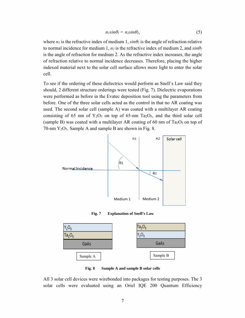
n1sinθ1 = n2sinθ2, (5)
where n1 is the refractive index of medium 1, sinθ1 is the angle of refraction relative to normal incidence for medium 1, n2 is the refractive index of medium 2, and sinθ2 is the angle of refraction for medium 2. As the refractive index increases, the angle of refraction relative to normal incidence decreases. Therefore, placing the higher indexed material next to the solar cell surface allows more light to enter the solar cell.
To see if the ordering of these dielectrics would perform as Snell’s Law said they should, 2 different structure orderings were tested (Fig. 7). Dielectric evaporations were performed as before in the Evatec deposition tool using the parameters from before. One of the three solar cells acted as the control in that no AR coating was used. The second solar cell (sample A) was coated with a multilayer AR coating consisting of 65 nm of Y2O3 on top of 65-nm Ta2O5, and the third solar cell (sample B) was coated with a multilayer AR coating of 60 nm of Ta2O5 on top of 70-nm Y2O3. Sample A and sample B are shown in Fig. 8.
Fig. 7 Explanation of Snell’s Law
Fig. 8 Sample A and sample B solar cells
All 3 solar cell devices were wirebonded into packages for testing purposes. The 3 solar cells were evaluated using an Oriel IQE 200 Quantum Efficiency
Medium 1 Medium 2
Sample A Sample B
8
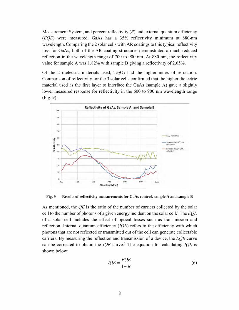
Measurement System, and percent reflectivity (R) and external quantum efficiency (EQE) were measured. GaAs has a 35% reflectivity minimum at 880-nm wavelength. Comparing the 2 solar cells with AR coatings to this typical reflectivity loss for GaAs, both of the AR coating structures demonstrated a much reduced reflection in the wavelength range of 700 to 900 nm. At 880 nm, the reflectivity value for sample A was 1.82% with sample B giving a reflectivity of 2.65%.
Of the 2 dielectric materials used, Ta2O5 had the higher index of refraction. Comparison of reflectivity for the 3 solar cells confirmed that the higher dielectric material used as the first layer to interface the GaAs (sample A) gave a slightly lower measured response for reflectivity in the 600 to 900 nm wavelength range (Fig. 9).
Fig. 9 Results of reflectivity measurements for GaAs control, sample A and sample B
As mentioned, the QE is the ratio of the number of carriers collected by the solar cell to the number of photons of a given energy incident on the solar cell.1 The EQE of a solar cell includes the effect of optical losses such as transmission and reflection. Internal quantum efficiency (IQE) refers to the efficiency with which photons that are not reflected or transmitted out of the cell can generate collectable carriers. By measuring the reflection and transmission of a device, the EQE curve can be corrected to obtain the IQE curve.1 The equation for calculating IQE is shown below:
R
EQEIQE−
=1
(6)

9
However, for measuring the effectiviness of these multi-layer AR coatings in reducing optical losses, EQE was the more important of the 2 measurements in characterizing the performance of these solar cells. The results of the EQE measurements are shown in Fig. 10.
Fig. 10 EQE measurements for GaAs solar cell control, sample A and sample B
As the data show, EQE values increased for both AR-coated GaAs solar cell devices, with a peak value in the 800-nm wavelength region. Sample A demonstrated the most improvement, with a slightly higher EQE value in the 600–820 nm region. This increase in EQE suggests that the actual power of the solar cell device will also increase.
3. Conclusion
A process for calculating the correct index of refraction of an as-deposited dielectric material for use as an AR coating was developed. Two dielectrics with reported refractive indices were individually deposited on to GaAs substrates and characterized. The corrected index of refractions for the dielectrics Y2O3 and Ta2O5 were calculated. Two multi-layer AR structures were designed and fabricated using these dielectric materials. They were deposited onto real GaAs solar cell devices and characterization of the AR coatings performed. Both multi-layer AR structure designs were found to be effective in substantially reducing the surface reflection off of the GaAs solar cells in the 600 to 900 nm wavelength spectral range. This reduction in optical loss enhanced the absorption of charge carriers into the active

10
region of the solar cell devices, as seen in the EQE measurement results. A difference in efficiency was seen between the 2 AR multi-layer structures as well, with the higher indexed Ta2O5 next to the solar cell demonstrating a higher EQE value in the wavelength spectral range of 600 to 820 nm. This result is dictated by Snell’s Law.
11
4. References
1. Honsberg C, Bowden S. PVCDROM [accessed 2015] www.pveducation.org.
2. Polyanskiy MN. Refractive index database. [accessed Feb. 29 2015]. www.Refractiveindex.info.
3. Nigara Y. Measurement of the optical constants of yttrium oxide. Jpn. J. Appl. Phys. 1968;7;404–408.
4. Gao L, Lemarchand F, Lequime M. Exploitation of multiple incidences spectrometric measurements for thin film reverse engineering. Opt. Express. 2012;20:15734–15751. (Numerical data kindly provided by F. Lemarchand)
5. www.britannica.com/photvoltaics
6. Gray Jeffery. The Physics of the Solar Cell, Chapter 3, Handbook of Photovoltaic Science and Engineering, second edition, John Wiley and Sons, Ltd, 2011
7. Hovhannisyan AS. Single-layer antireflection coatings for GaAs solar cells. Journal of Contemporary Physics. 2008;3(3):136–138.

12
List of Symbols, Abbreviations, and Acronyms
AlGaAs aluminum gallium arsenide
AR anti-reflective
Au gold
Cr chromium
EQE external quantum efficiency
GaAs gallium arsenide
IQE internal quantum efficiency
MBE molecular beam epitaxial
O2 oxygen
PV photovoltaic
QE quantum efficiency
Sn tin
Ta2O5 tantalum pentoxide
Y2O3 yttrium oxide
13
1 DEFENSE TECHNICAL (PDF) INFORMATION CTR DTIC OCA 2 DIRECTOR (PDF) US ARMY RESEARCH LAB RDRL CIO LL IMAL HRA MAIL & RECORDS MGMT 1 GOVT PRINTG OFC (PDF) A MALHOTRA 1 DIRECTOR (PDF) US ARMY RESEARCH LAB RDRL SEE I K OLVER

14
INTENTIONALLY LEFT BLANK.