Embed Size (px)
Citation preview
Cheiron Synchrotron Summer School
Detectors for Synchrotron Radiation
Chris HallMonash University
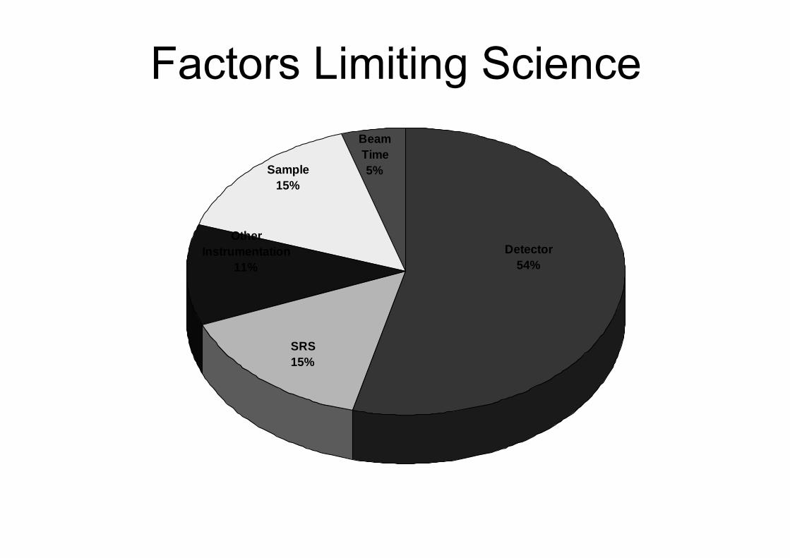
Factors Limiting Science
SRS15%
Detector54%
Sample15%
Other Instrumentation
11%
BeamTime5%
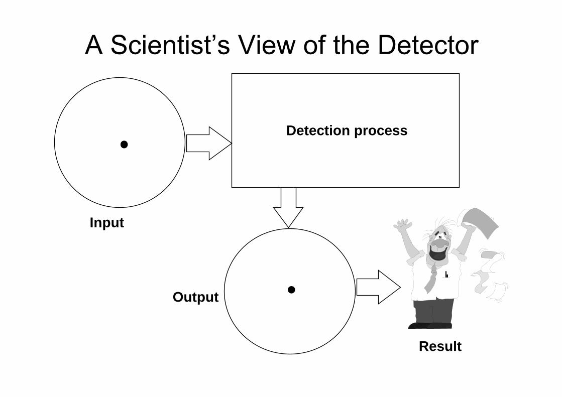
A Scientist’s View of the Detector
Input
Output
Detection process
Result
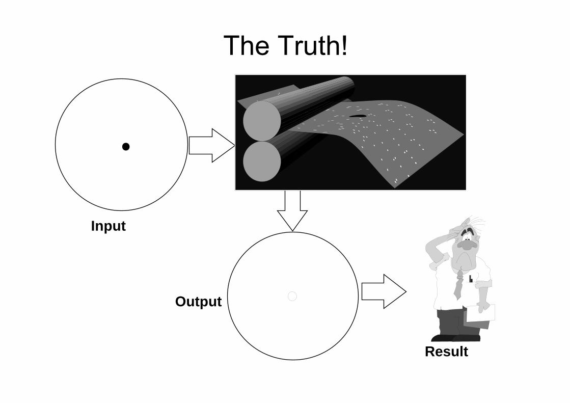
The Truth!
Input
Output
Result
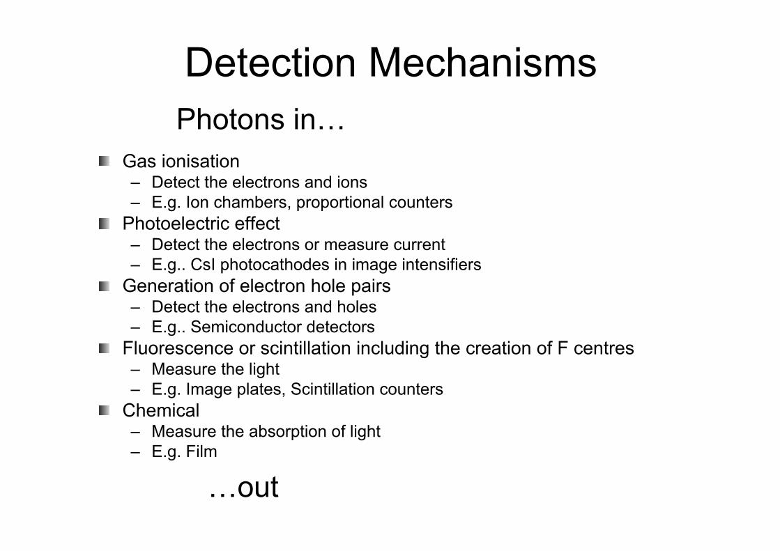
Detection Mechanisms
Gas ionisation– Detect the electrons and ions– E.g. Ion chambers, proportional counters
Photoelectric effect– Detect the electrons or measure current– E.g.. CsI photocathodes in image intensifiers
Generation of electron hole pairs– Detect the electrons and holes– E.g.. Semiconductor detectors
Fluorescence or scintillation including the creation of F centres– Measure the light– E.g. Image plates, Scintillation counters
Chemical– Measure the absorption of light– E.g. Film
Photons in…
…out
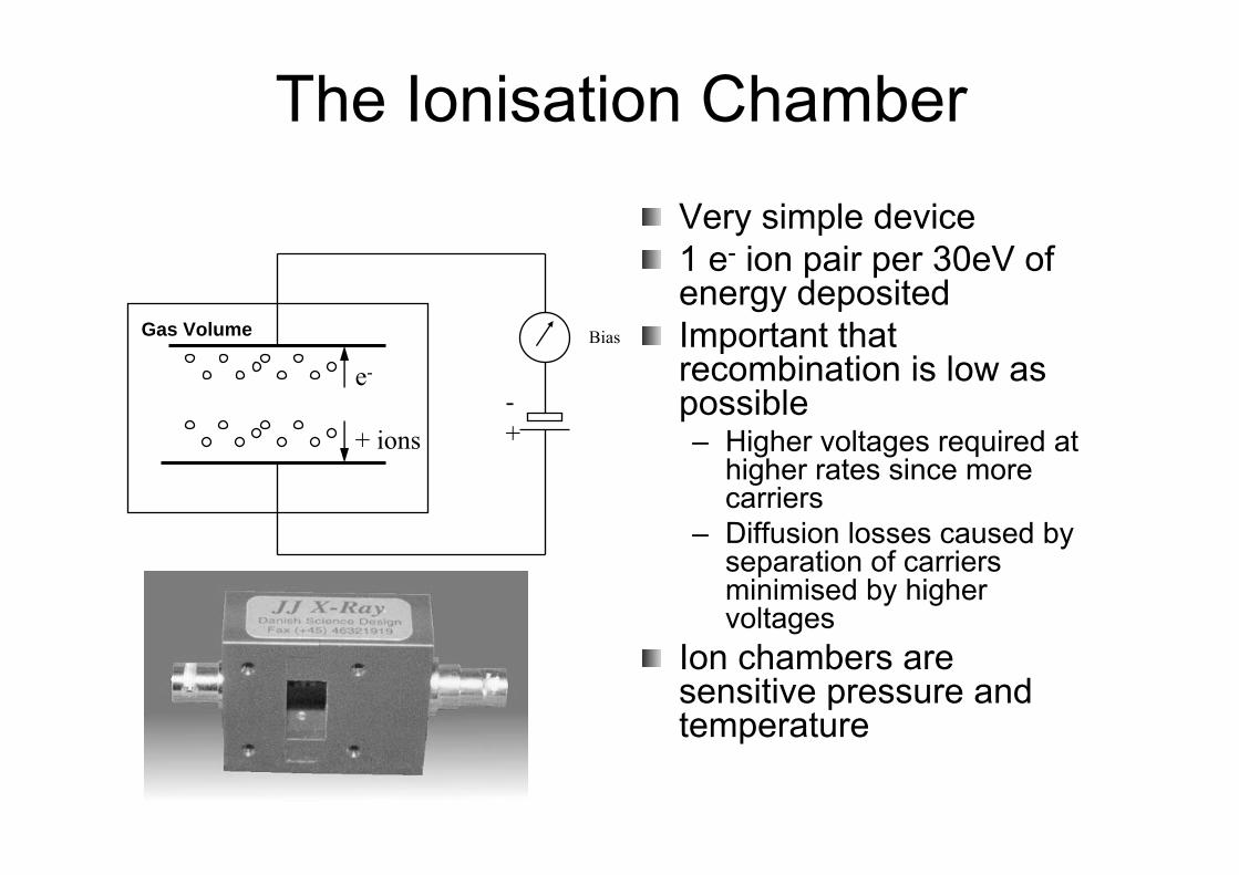
The Ionisation ChamberVery simple device1 e- ion pair per 30eV of energy depositedImportant that recombination is low as possible– Higher voltages required at
higher rates since more carriers
– Diffusion losses caused by separation of carriers minimised by higher voltages
Ion chambers are sensitive pressure and temperature
Gas Volume Bias
-+
e-
+ ions
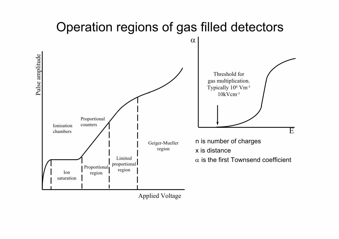
Operation regions of gas filled detectorsPu
lse
ampl
itude
Applied Voltage
Ion saturation
Proportional region
Limited proportional
region
Geiger-Mueller region
Ionisation chambers
Proportional counters
α
E
Threshold forgas multiplication.Typically 106 Vm-1
10kVcm-1
n is number of chargesx is distanceα is the first Townsend coefficient
dxn
dn α=
xenxn α)0()( =

Field Variation
Distance from wire
Fiel
d
E(r) ~ 1/r
Cathode
Anode
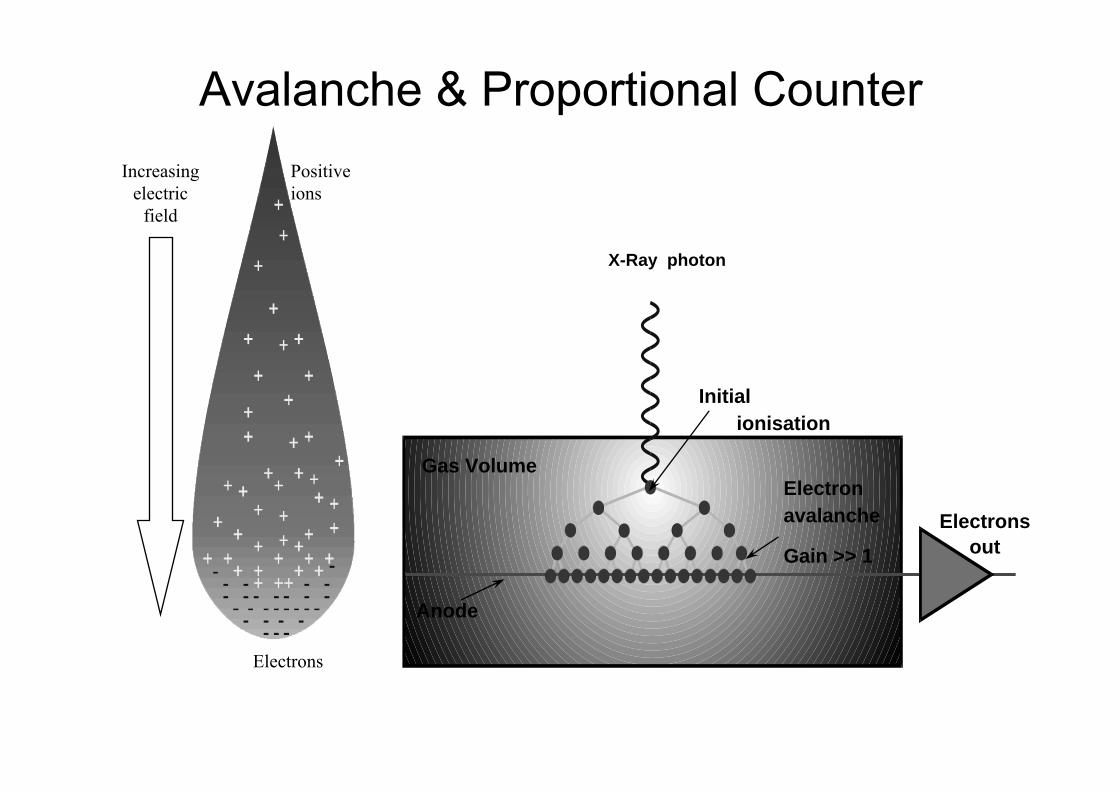
Electrons
Positive ions
Avalanche & Proportional CounterIncreasing
electric field
X-Ray photon
Initial ionisation
Electron avalanche
Gain >> 1
Anode
Electrons out
Gas Volume
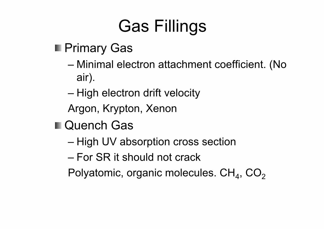
Gas FillingsPrimary Gas– Minimal electron attachment coefficient. (No
air).– High electron drift velocityArgon, Krypton, Xenon
Quench Gas– High UV absorption cross section– For SR it should not crackPolyatomic, organic molecules. CH4, CO2
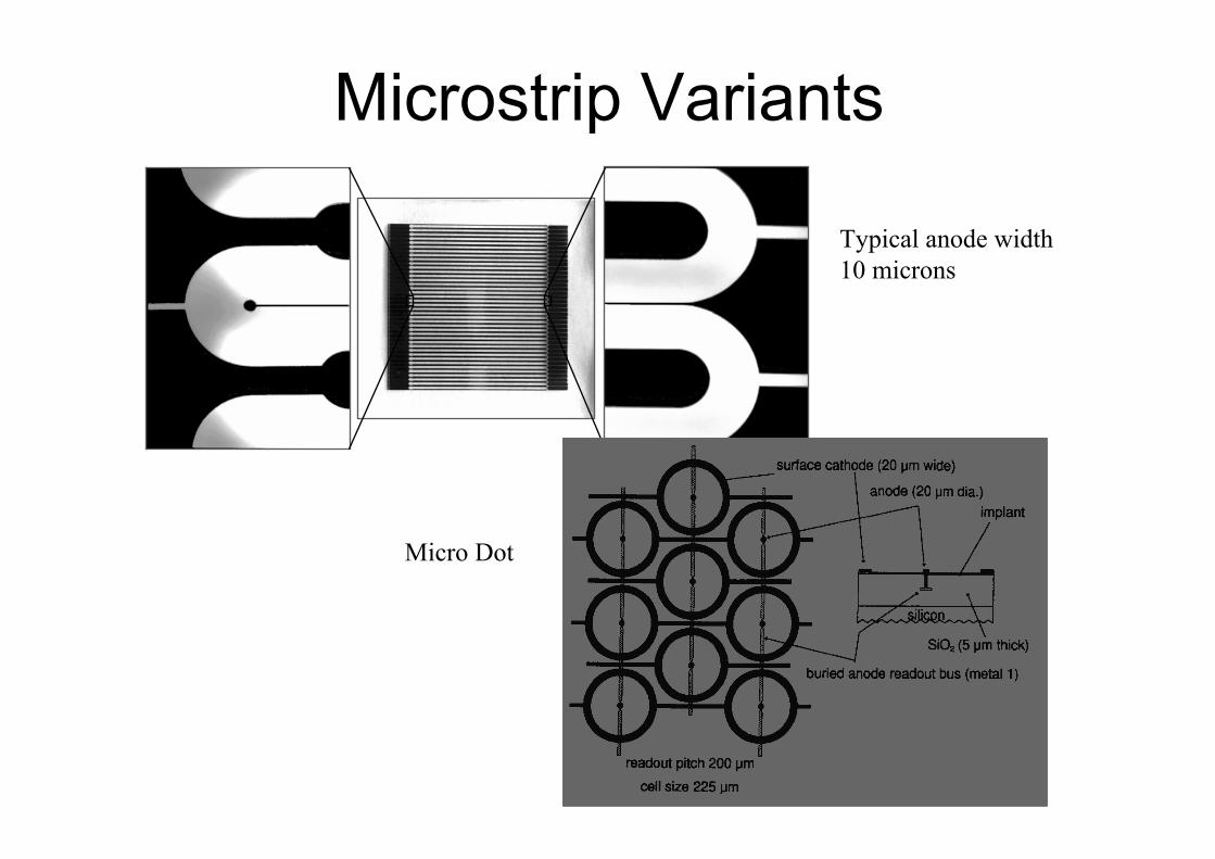
Microstrip Variants
Micro Dot
Typical anode width10 microns

Efficiencies
0
0.1
0.2
0.3
0.4
0.5
0.6
0.7
0.8
0.9
1
0 5000 10000 15000 20000 25000 30000
Energy (eV)
Tran
smis
sion
0
0.1
0.2
0.3
0.4
0.5
0.6
0.7
0.8
0.9
1Absorption
BeAlPolimidePolyropyleneArKrXe
Gas thickness 1cmWindows 100μm
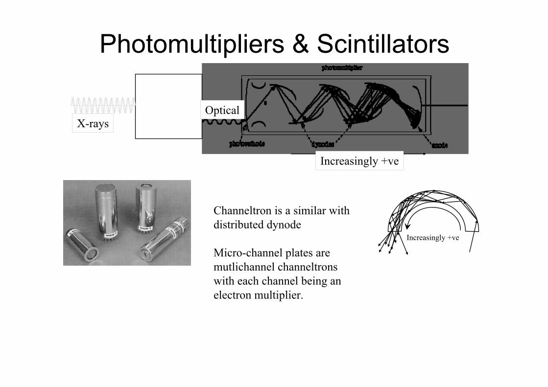
Photomultipliers & Scintillators
X-raysOptical
Increasingly +ve
Channeltron is a similar with distributed dynode
Micro-channel plates are mutlichannel channeltronswith each channel being an electron multiplier.
Increasingly +ve
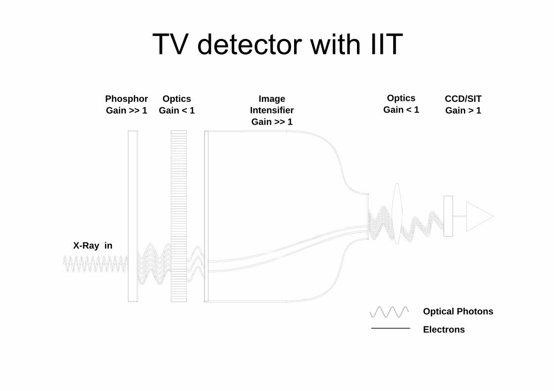
TV detector with IITImage
IntensifierGain >> 1
X-Ray in
OpticsGain < 1
PhosphorGain >> 1
CCD/SITGain > 1
Optical Photons
Electrons
OpticsGain < 1
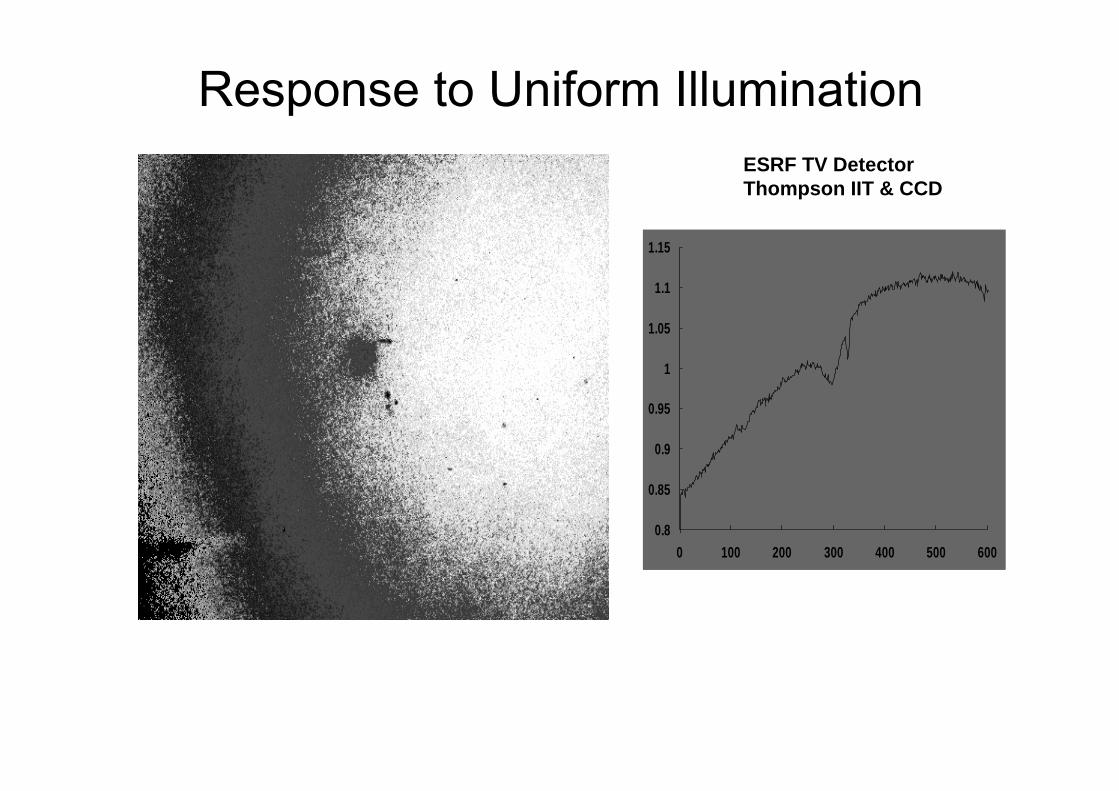
Response to Uniform IlluminationESRF TV DetectorThompson IIT & CCD
0.8
0.85
0.9
0.95
1
1.05
1.1
1.15
0 100 200 300 400 500 600
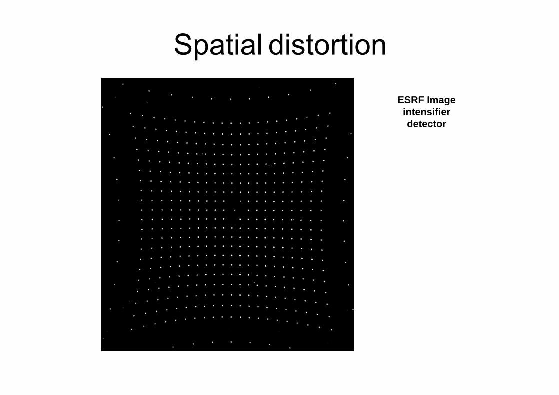
Spatial distortionESRF Image intensifierdetector
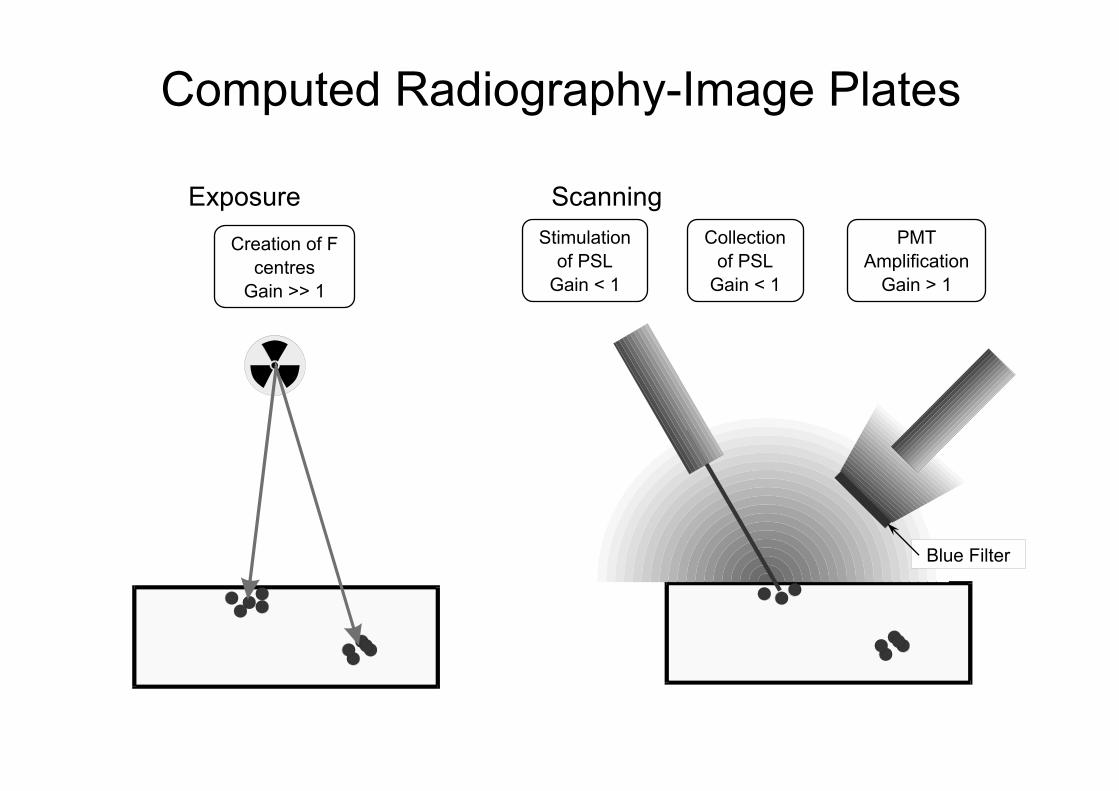
Computed Radiography-Image Plates
Stimulation of PSL
Gain < 1
Collection of PSL
Gain < 1
Creation of F centres
Gain >> 1
PMT Amplification
Gain > 1
Blue Filter
Exposure Scanning
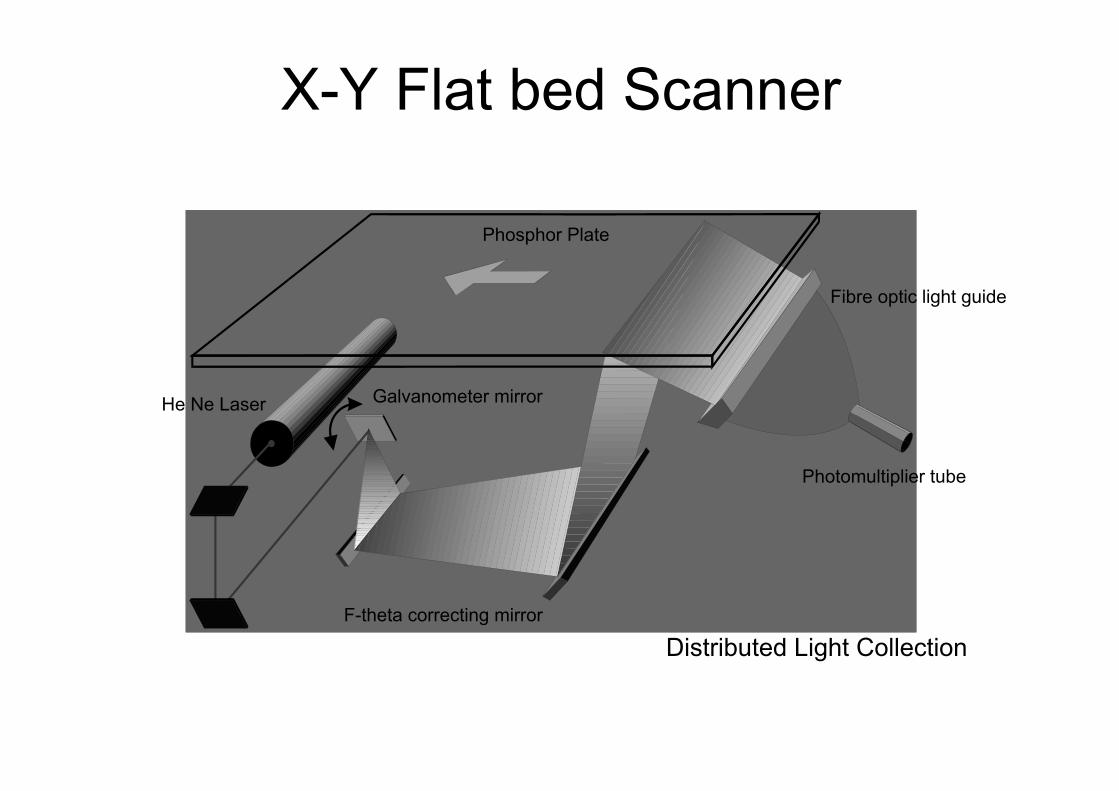
X-Y Flat bed Scanner
Phosphor Plate
He Ne Laser
F-theta correcting mirror
Fibre optic light guide
Photomultiplier tube
Galvanometer mirror
Distributed Light Collection
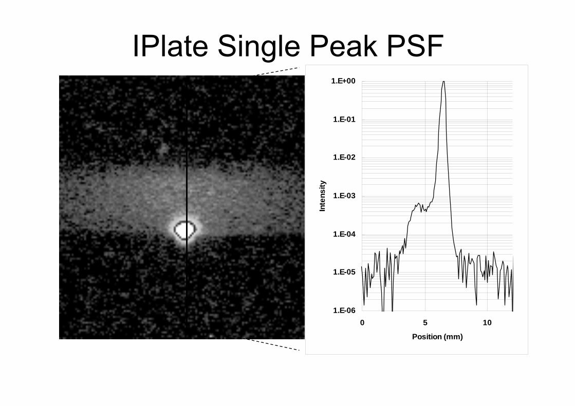
IPlate Single Peak PSF
1.E-06
1.E-05
1.E-04
1.E-03
1.E-02
1.E-01
1.E+00
0 5 10
Position (mm)
Inte
nsity
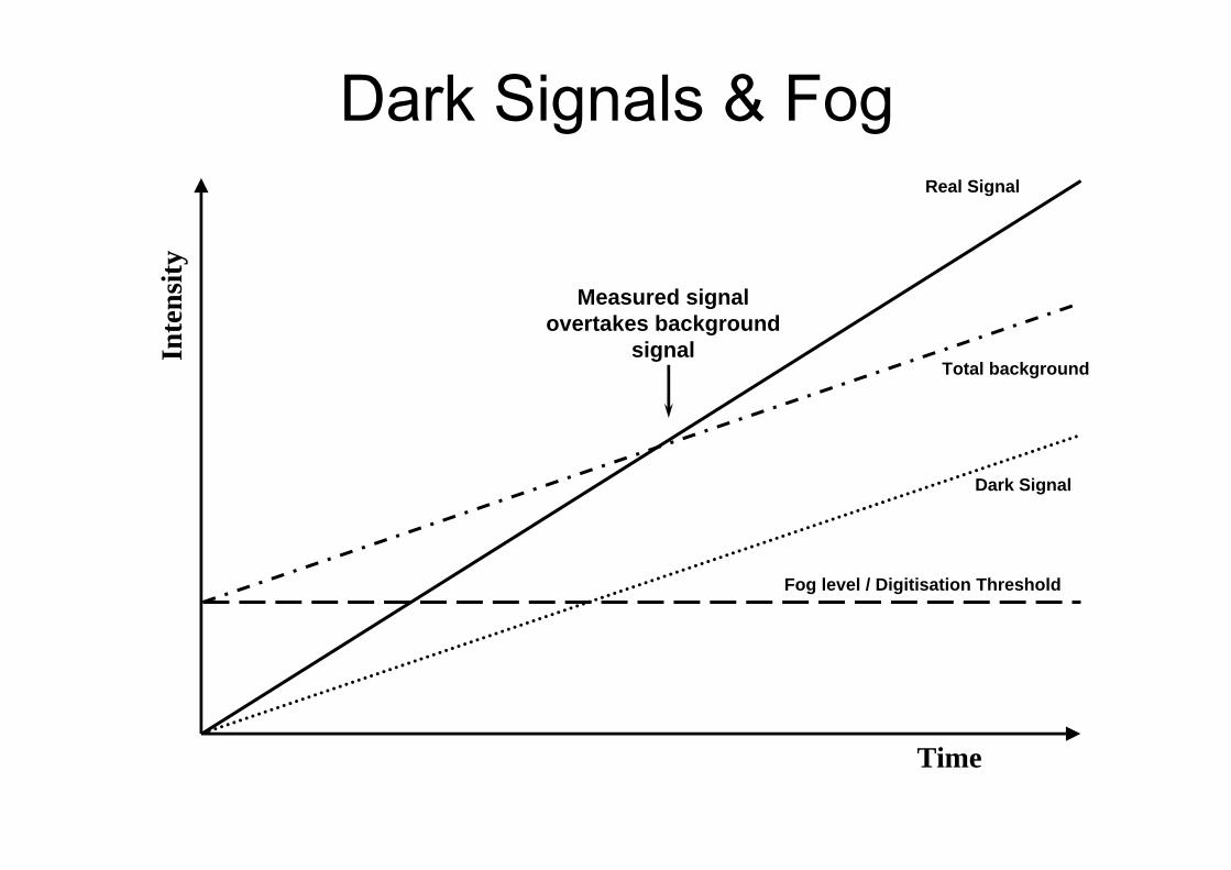
Dark Signals & Fog
Measured signal overtakes background
signal
Time
Inte
nsity
Fog level / Digitisation Threshold
Total background
Dark Signal
Real Signal
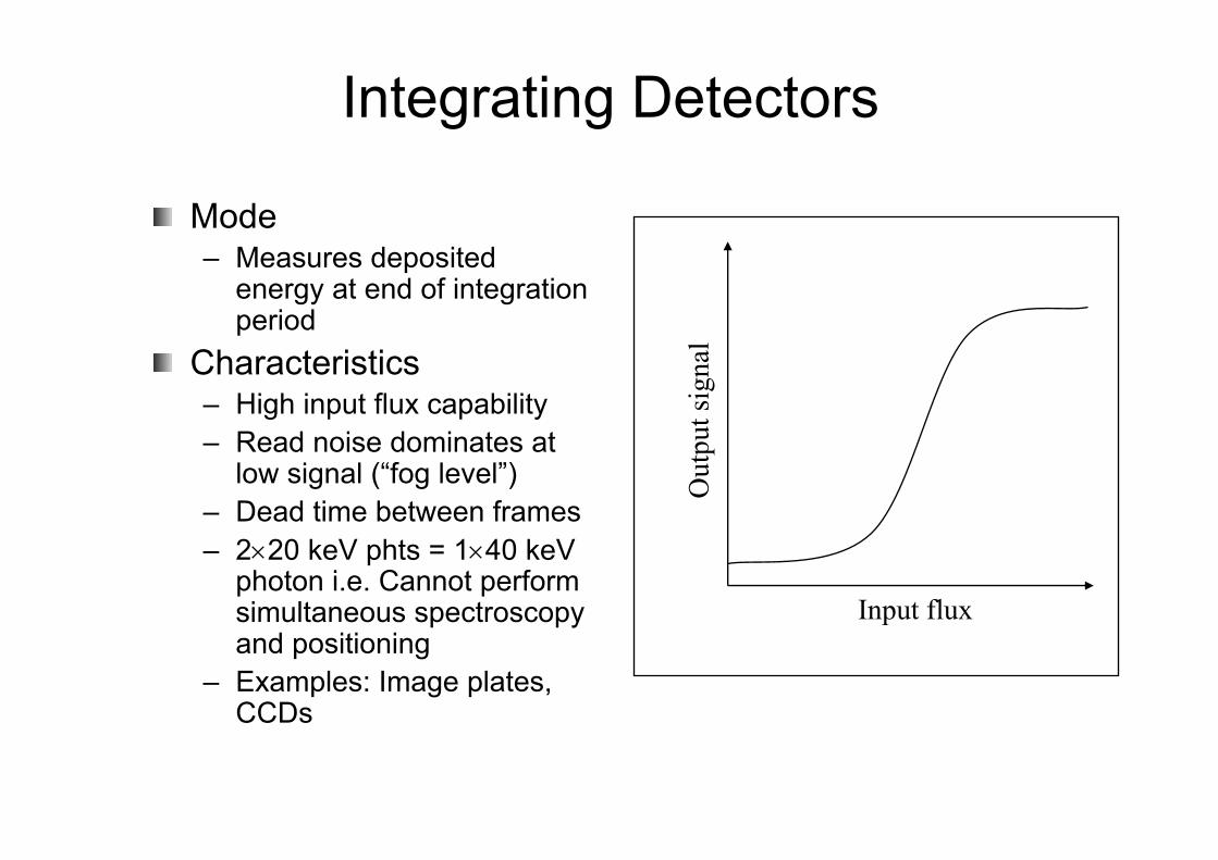
Integrating Detectors
Mode– Measures deposited
energy at end of integration period
Characteristics– High input flux capability – Read noise dominates at
low signal (“fog level”)– Dead time between frames– 2×20 keV phts = 1×40 keV
photon i.e. Cannot perform simultaneous spectroscopy and positioning
– Examples: Image plates, CCDs
Input flux
Out
put s
igna
l
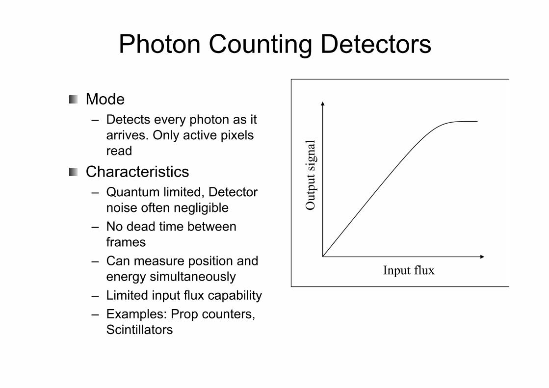
Photon Counting Detectors
Mode– Detects every photon as it
arrives. Only active pixels read
Characteristics– Quantum limited, Detector
noise often negligible– No dead time between
frames– Can measure position and
energy simultaneously– Limited input flux capability– Examples: Prop counters,
Scintillators
Input flux
Out
put s
igna
l
10
100
1000
10000
100000
0 20 40 60 80 100 120 140 160
Position (mm)
Inte
nsity
(Pho
tons
/mm
^2)
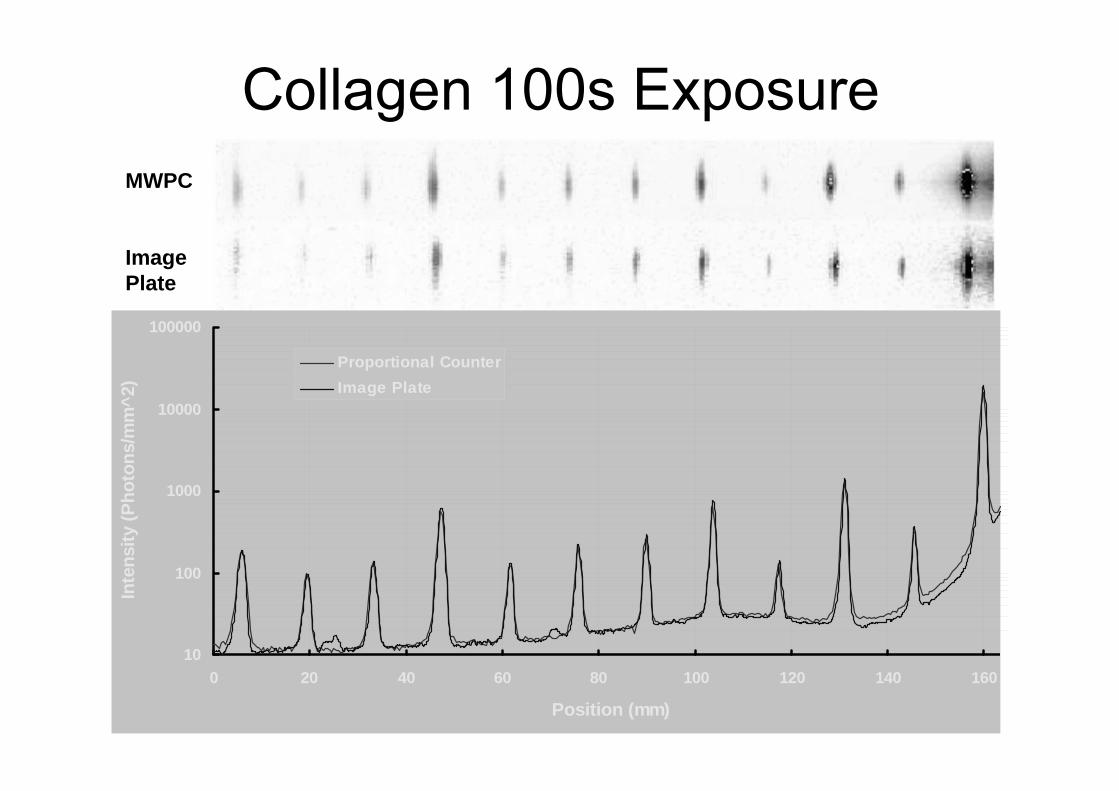
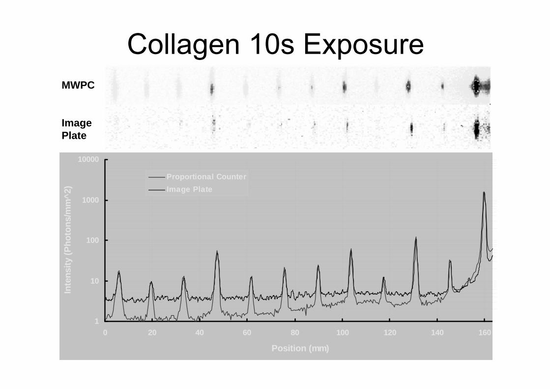
Proportional CounterImage Plate
Collagen 100s ExposureMWPC
Image Plate
1
10
100
1000
10000
0 20 40 60 80 100 120 140 160
Position (mm)
Inte
nsity
(Pho
tons
/mm
^2)
Proportional CounterImage Plate
Collagen 10s ExposureMWPC
Image Plate
0.01
0.1
1
10
100
0 20 40 60 80 100 120 140 160
Position (mm)
Inte
nsity
(Pho
tons
/mm
^2)
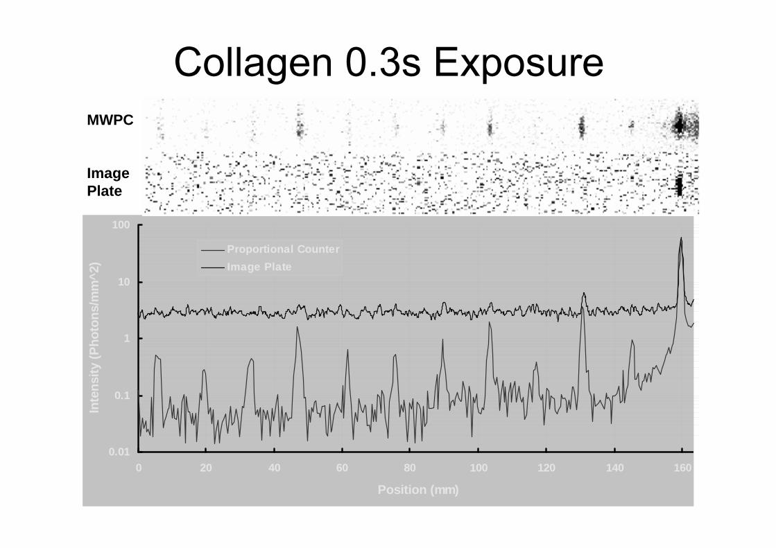
Proportional CounterImage Plate
Collagen 0.3s ExposureMWPC
Image Plate
-1
-0.5
0
0.5
1
1.5
-1
0
1
2
3
4
5
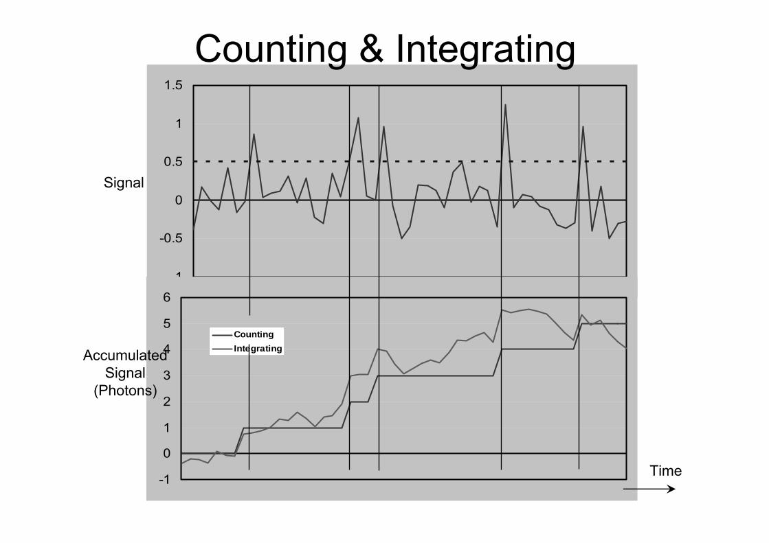
6
CountingIntegrating
Counting & Integrating
Signal
AccumulatedSignal
(Photons)
Time
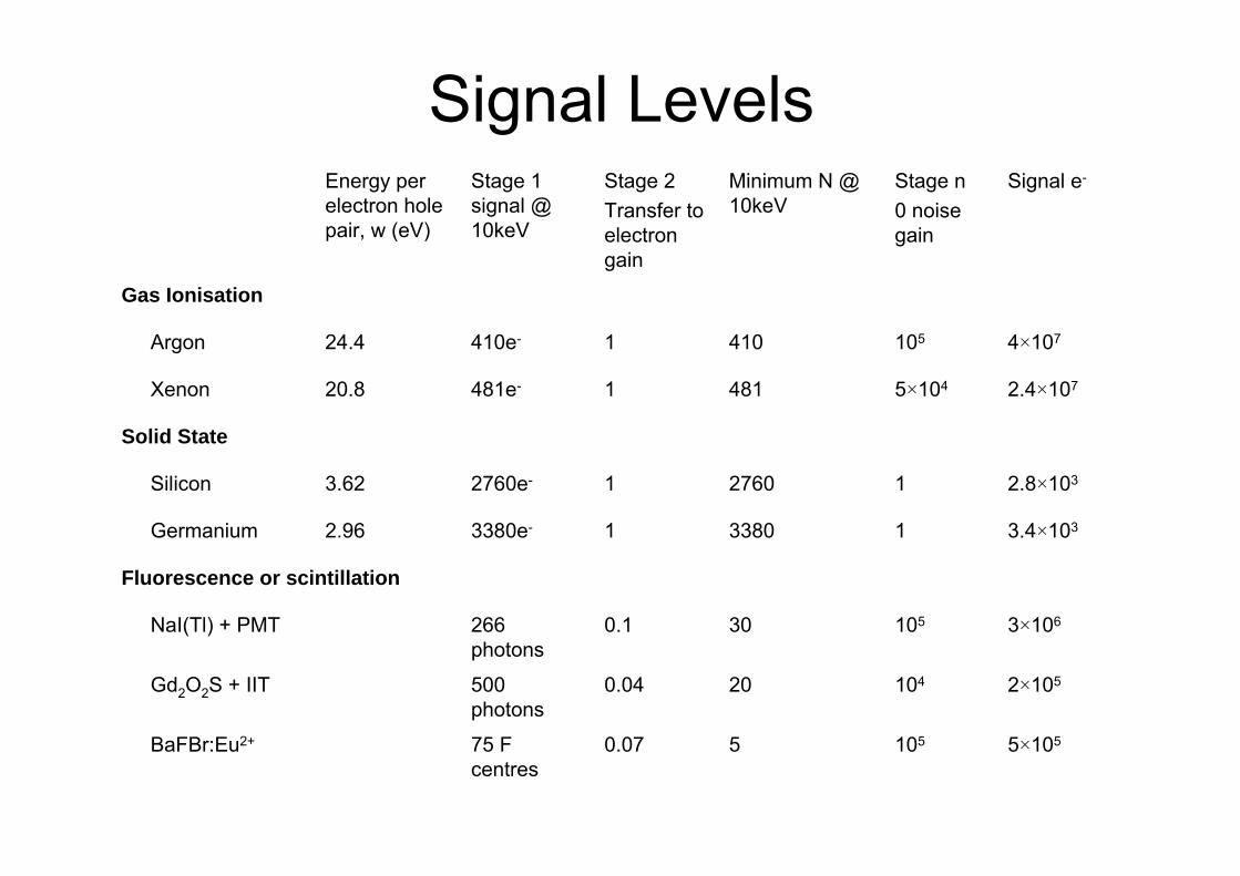
Signal Levels
0.07
0.04
0.1
1
1
1
1
Stage 2Transfer to electron gain
Gas Ionisation
5×105105575 F centres
BaFBr:Eu2+
2×10510420500 photons
Gd2O2S + IIT
266 photons
3380e-
2760e-
481e-
410e-
Stage 1 signal @ 10keV
Fluorescence or scintillation
Solid State
3×10610530NaI(Tl) + PMT
3.4×103133802.96Germanium
2.8×103127603.62Silicon
2.4×1075×10448120.8Xenon
4×10710541024.4Argon
Signal e-Stage n0 noise gain
Minimum N @ 10keV
Energy per electron hole pair, w (eV)

Spectral Resolution
Average number of carriers, N = E/w where w is energy to create electron hole/ion pairPoisson statistics: σ = 1/√N ΔE/E = 2.355σ = 2.355(E/w)-½ = 2.355(w/E)½
For Ge, w= 3eV so at 10keV ΔE/E = 4%For Ar, w= 25eV so at 10keV ΔE/E = 12%
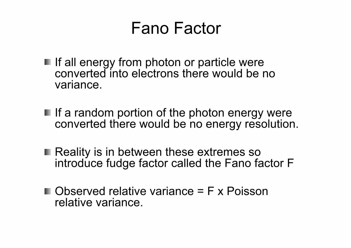
Fano Factor
If all energy from photon or particle were converted into electrons there would be no variance.
If a random portion of the photon energy were converted there would be no energy resolution.
Reality is in between these extremes so introduce fudge factor called the Fano factor F
Observed relative variance = F x Poisson relative variance.
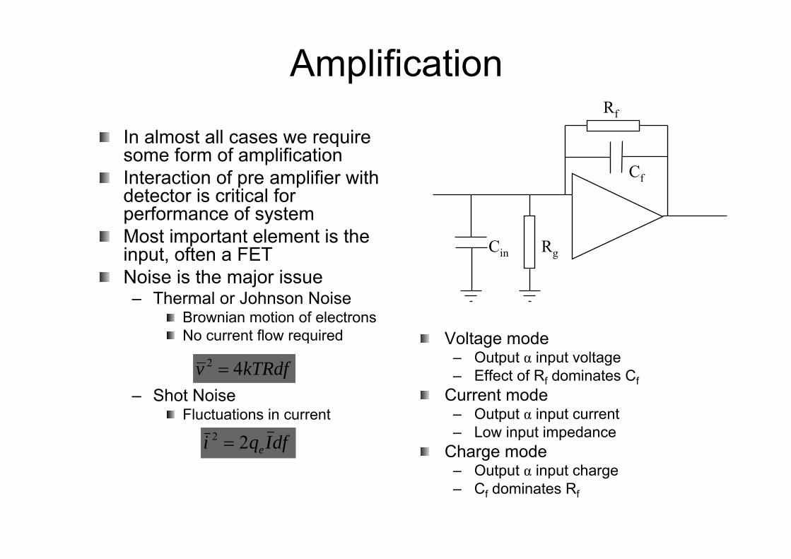
Amplification
In almost all cases we require some form of amplificationInteraction of pre amplifier with detector is critical for performance of systemMost important element is the input, often a FETNoise is the major issue– Thermal or Johnson Noise
Brownian motion of electronsNo current flow required
– Shot NoiseFluctuations in current
Voltage mode– Output α input voltage– Effect of Rf dominates Cf
Current mode– Output α input current– Low input impedance
Charge mode– Output α input charge– Cf dominates Rf
kTRdfv 42 =
dfIqi e22 =
RgCin
Rf
Cf
Equivalent Noise Charge
Low noise is no use if signal is lowIntroduce ENC which is that signal charge that will produce the same output as the RMS noise
Wherek = Boltzman’s constantT = temperaturee = the electronic chargeRg = Load resistance and/or feedback resistancegm = transconductance of input FET. (Links current in to voltage out)τ = Rise time of amplifierCin = input / stray and feedback capacitance
Note that ENC is directly related to energy resolutionFWHM(keV) = 2.355×10⁻³ ENC/ew where w is the energy per electron
( )⎥⎥⎦
⎤
⎢⎢⎣
⎡++=
τττ
m
inD
g gCkTeI
RkTENC
242924.0
22
Noise Dependence
τ optimum at
Choosing optimum τ gives best noise performance but may not be fast enoughWe often have to sacrifice energy resolution for speed
( ) ( ) inDef
mopt C
IqRkTgkT
2
422
⎥⎥⎦
⎤
⎢⎢⎣
⎡
+=τ
Optimum τ
Rg as large as possible ~ 1010ΩID (leakage) as small as possible– For Ge cooling is vital
Low T is goodCin as small as possible (note that this includes Cf)gm as large as possible but this affects Cin

Optimum Spectral Resolution
Low capacitance– Small planar < 1pF
Low leakage currentsMaximise Rg and/or Rf– Remove altogether so Rf = ∞
Use optical resetCan improve FWHM by 20%
Detector
LED
Cf
Bias
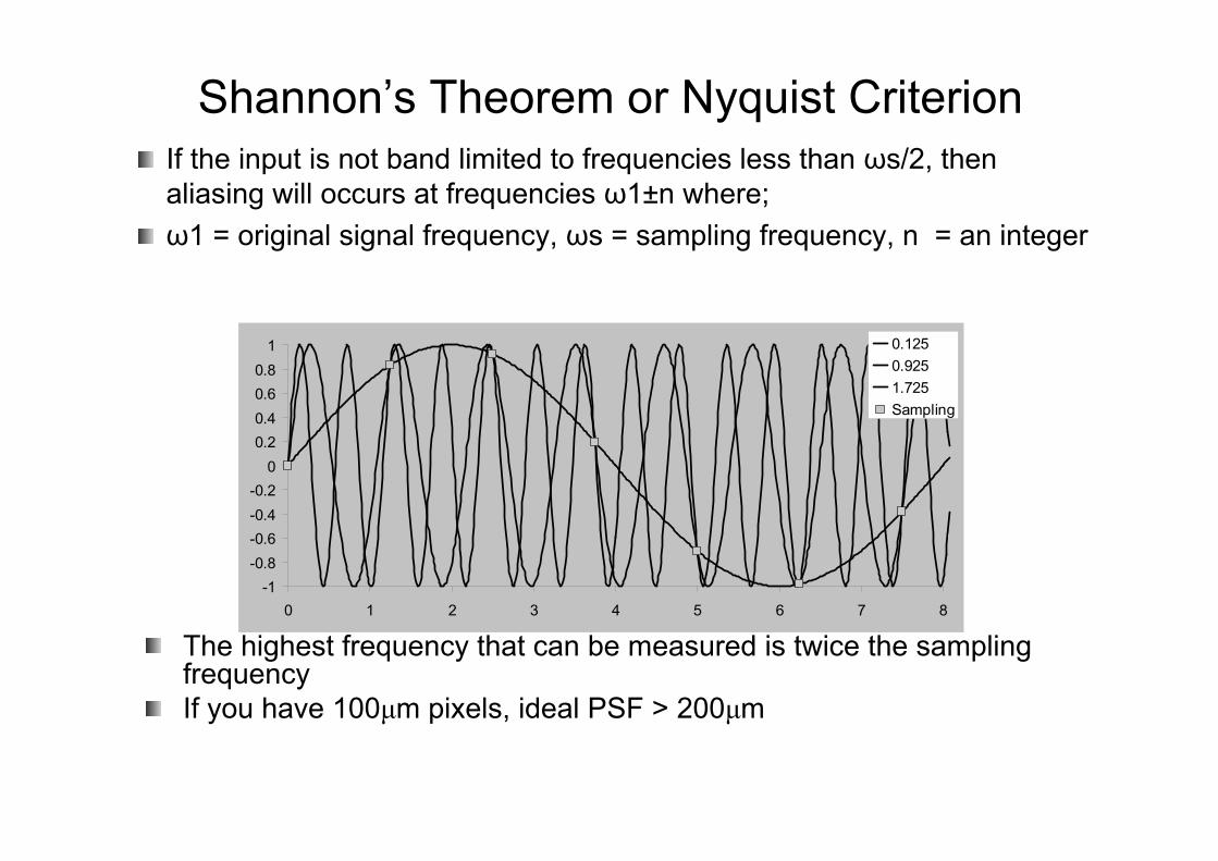
Shannon’s Theorem or Nyquist Criterion
The highest frequency that can be measured is twice the samplingfrequencyIf you have 100μm pixels, ideal PSF > 200μm
-1-0.8-0.6-0.4-0.2
00.20.40.60.8
1
0 1 2 3 4 5 6 7 8
0.1250.9251.725Sampling
If the input is not band limited to frequencies less than ωs/2, then aliasing will occurs at frequencies ω1±n where;ω1 = original signal frequency, ωs = sampling frequency, n = an integer
Performance Measure - DQE
incidealNon NSNR <−Real detector
idealNonSNRNEQ −= 2
Can define Nphotons that describes real SNR
2
2
inc
idealNon
inc SNRSNR
NNEQDQE −==
Ratio of this to Ninc is a measure of efficiency
incinc SNRN 2=∴Perfect detector incinc NSNR =
Note that DQE is f(spatial and spectral frequencies)
Effect of Peak Width
-20
0
20
40
60
80
100
120
Position
1 pixe l2 pixe l5 pixe l10pixe l
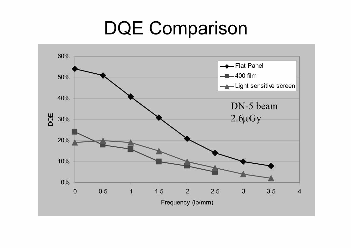
DQE Comparison
0%
10%
20%
30%
40%
50%
60%
0 0.5 1 1.5 2 2.5 3 3.5 4
Frequency (lp/mm)
DQ
E
Flat Panel400 filmLight sensitive screen
DN-5 beam2.6μGy
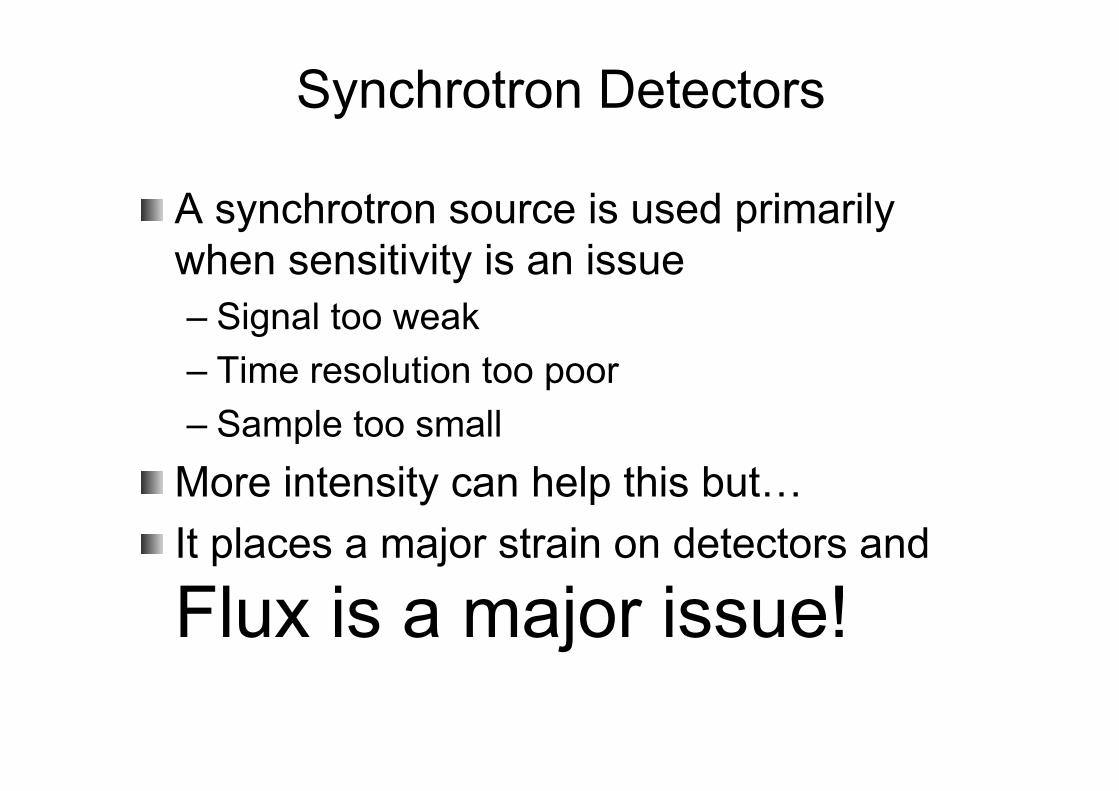
Synchrotron Detectors
A synchrotron source is used primarily when sensitivity is an issue– Signal too weak– Time resolution too poor– Sample too small
More intensity can help this but…It places a major strain on detectors and
Flux is a major issue!
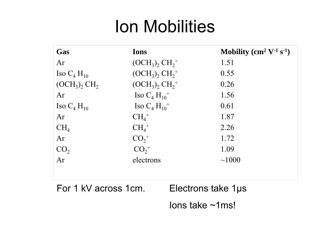
Ion MobilitiesGas Ions Mobility (cm2 V-1 s-1)Ar (OCH3)2 CH2
+ 1.51Iso C4 H10 (OCH3)2 CH2
+ 0.55(OCH3)2 CH2 (OCH3)2 CH2
+ 0.26Ar Iso C4 H10
+ 1.56Iso C4 H10 Iso C4 H10
+ 0.61Ar CH4
+ 1.87CH4 CH4
+ 2.26Ar CO2
+ 1.72CO2 CO2
+ 1.09Ar electrons ~1000
For 1 kV across 1cm. Electrons take 1µs
Ions take ~1ms!
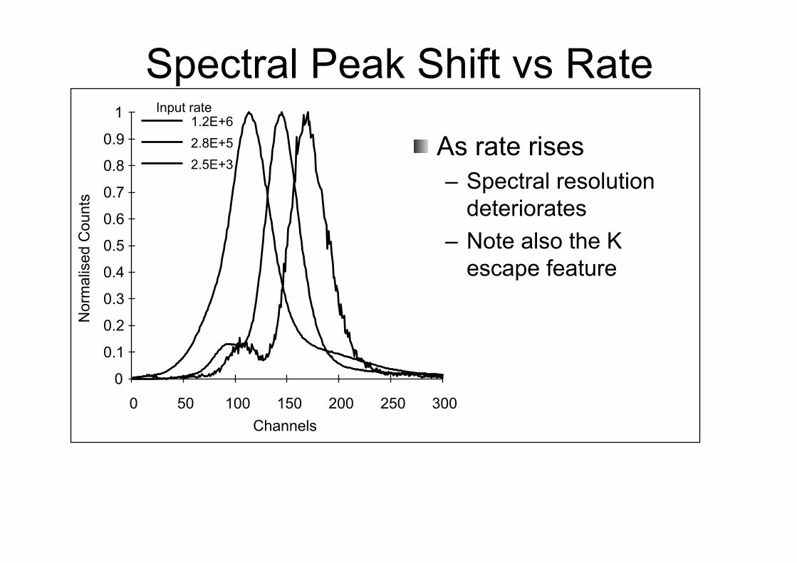
Spectral Peak Shift vs Rate
As rate rises– Spectral resolution
deteriorates– Note also the K
escape feature
Channels
0
0.1
0.2
0.3
0.4
0.5
0.6
0.7
0.8
0.9
1
0 50 100 150 200 250 300
1.2E+62.8E+52.5E+3
Nor
mal
ised
Cou
nts
Input rate
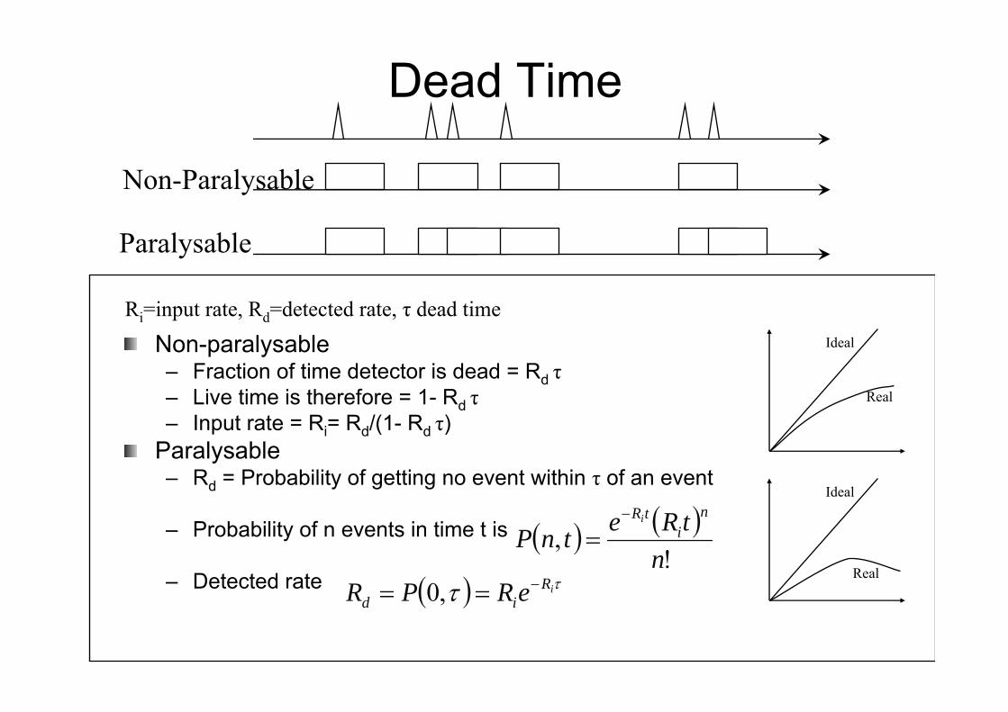
Dead Time
Non-paralysable– Fraction of time detector is dead = Rd τ– Live time is therefore = 1- Rd τ– Input rate = Ri= Rd/(1- Rd τ)
Paralysable– Rd = Probability of getting no event within τ of an event
– Probability of n events in time t is
– Detected rate
Paralysable
Non-Paralysable
( ) ( )!
,n
tRetnPn
itRi−
=
( ) ττ iRid eRPR −== ,0
Ideal
Real
Ideal
Real
Ri=input rate, Rd=detected rate, τ dead time
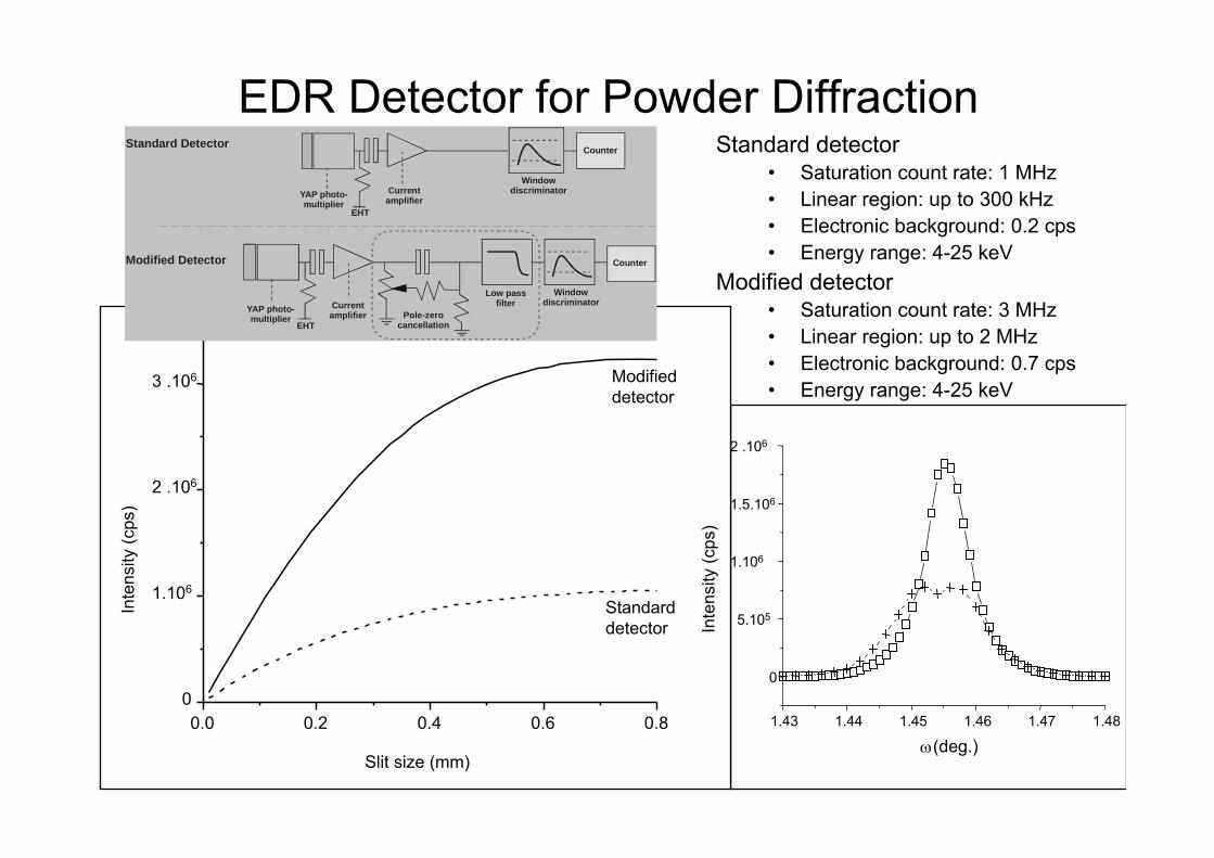
EDR Detector for Powder Diffraction
0.0 0.2 0.4 0.6 0.80
1.106
2 .106
3 .106 Modified detector
Inte
nsity
(cps
)
Slit size (mm)
Standard detector
1.43 1.44 1.45 1.46 1.47 1.48
0
5.105
1.106
1.5.106
2 .106
Inte
nsity
(cps
)
ω(deg.)
YAP photo-multiplier
Standard Detector
Modified Detector
YAP photo-multiplier
Current amplifier
Window discriminator
Pole-zero cancellation
Low pass filter
Window discriminator
EHT
EHT
Counter
Current amplifier
Counter Standard detector• Saturation count rate: 1 MHz• Linear region: up to 300 kHz• Electronic background: 0.2 cps• Energy range: 4-25 keV
Modified detector• Saturation count rate: 3 MHz• Linear region: up to 2 MHz• Electronic background: 0.7 cps• Energy range: 4-25 keV
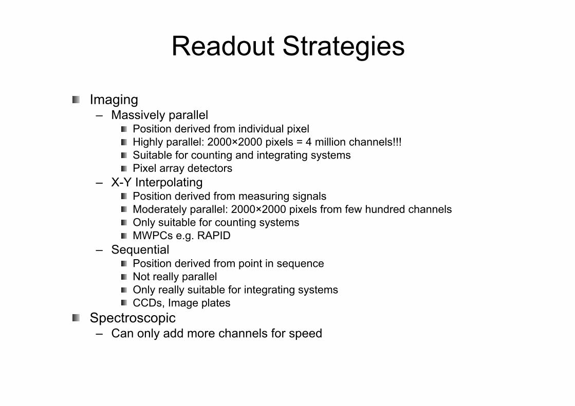
Readout Strategies
Imaging– Massively parallel
Position derived from individual pixelHighly parallel: 2000×2000 pixels = 4 million channels!!!Suitable for counting and integrating systemsPixel array detectors
– X-Y InterpolatingPosition derived from measuring signalsModerately parallel: 2000×2000 pixels from few hundred channelsOnly suitable for counting systemsMWPCs e.g. RAPID
– SequentialPosition derived from point in sequenceNot really parallelOnly really suitable for integrating systemsCCDs, Image plates
Spectroscopic– Can only add more channels for speed
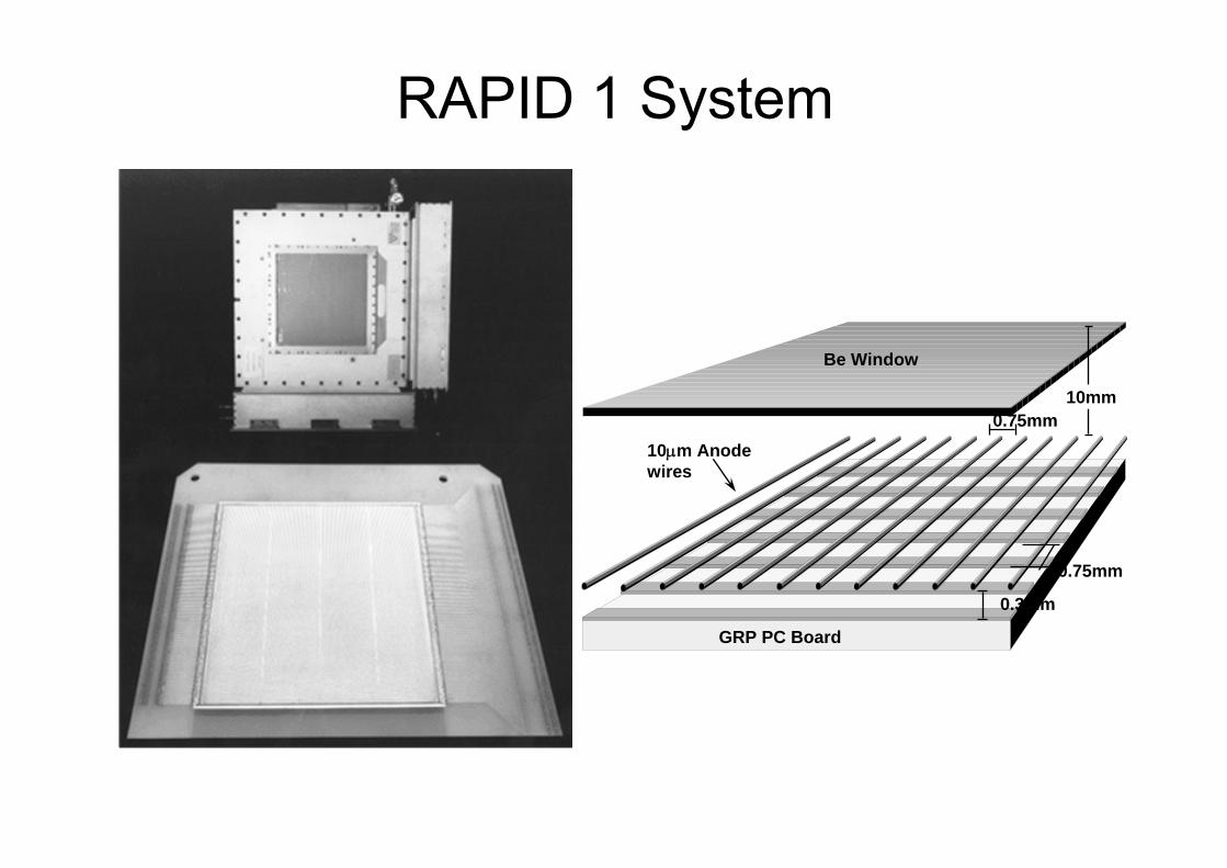
RAPID 1 System
Be Window
10μm Anode wires
0.3mm
0.75mm
GRP PC Board
0.75mm
10mm
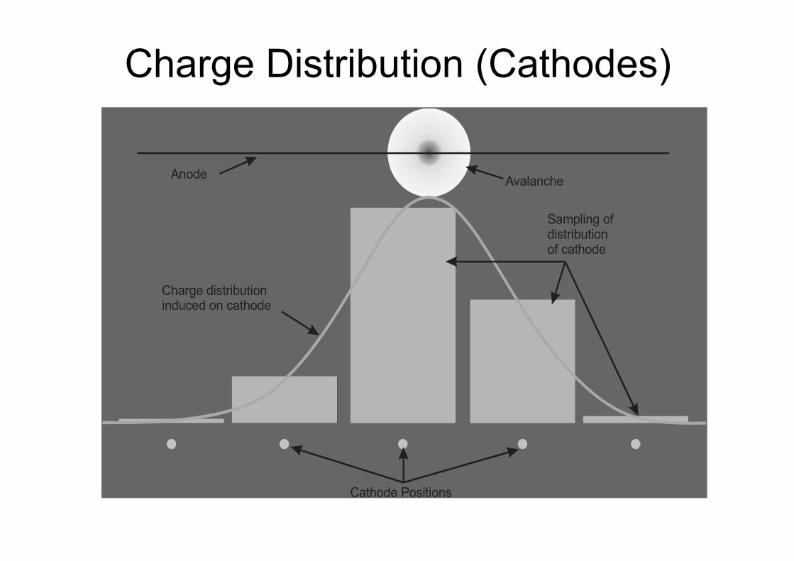
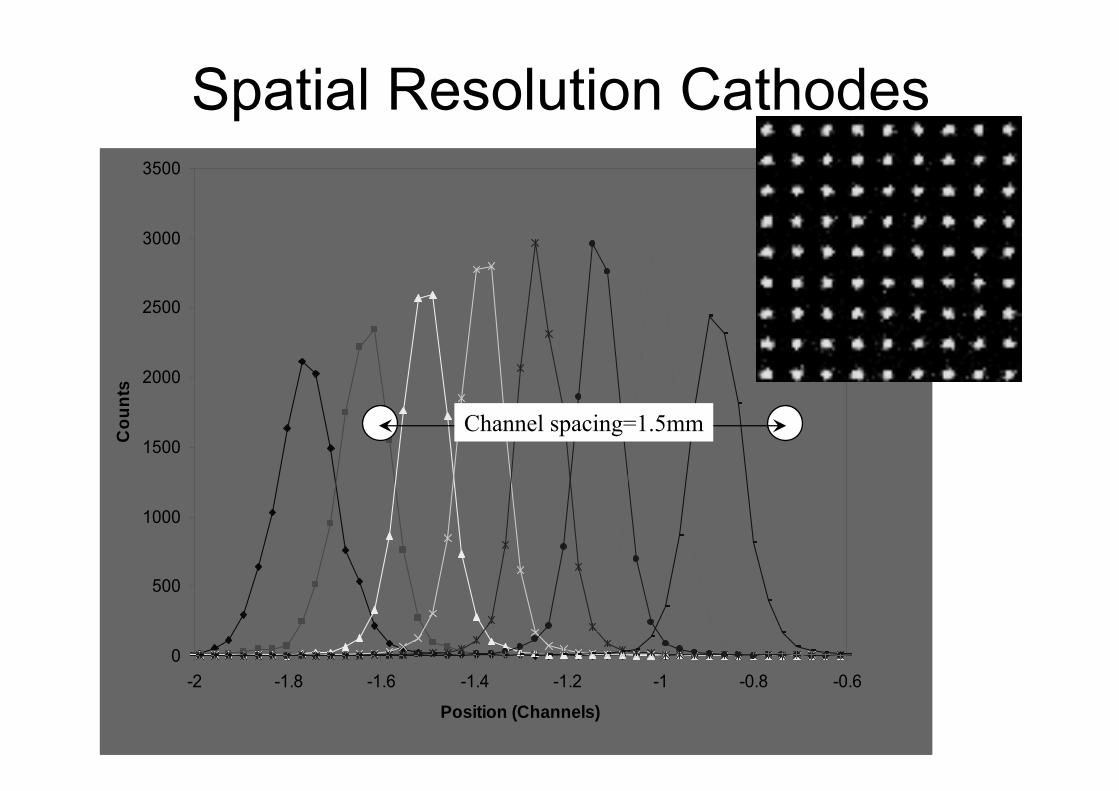
Charge Distribution (Cathodes)
Cathode Positions
AvalancheAnode
Charge distribution induced on cathode
Sampling ofdistributionof cathode
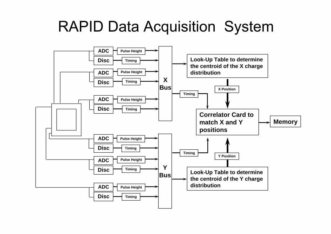
RAPID Data Acquisition System
Memory
XBus
Look-Up Table to determine the centroid of the X charge distribution
Look-Up Table to determine the centroid of the Y charge distribution
Correlator Card to match X and Y positions
Pulse Height
Timing
Pulse Height
Timing
Pulse Height
Timing
YBus
Pulse Height
Timing
Pulse Height
Timing
Pulse Height
Timing
X Position
Y Position
Timing
Timing
ADC
Disc
ADC
Disc
ADC
Disc
ADC
Disc
ADC
Disc
ADC
Disc
0
500
1000
1500
2000
2500
3000
3500
-2 -1.8 -1.6 -1.4 -1.2 -1 -0.8 -0.6
Position (Channels)
Cou
nts
Spatial Resolution Cathodes
Channel spacing=1.5mm
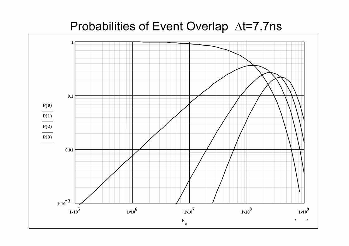
Probabilities of Event Overlap Δt=7.7ns
P 0( )
P 1( )
P 2( )
P 3( )
Ro
1 105 1 106 1 107 1 108 1 1091 10 3
0.01
0.1
1
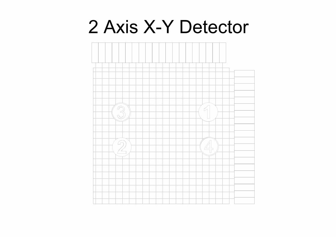
2 Axis X-Y Detector

Deadtime Correction
3 MHz Raw Image Corrected 3MHz ImageLow Rate Image
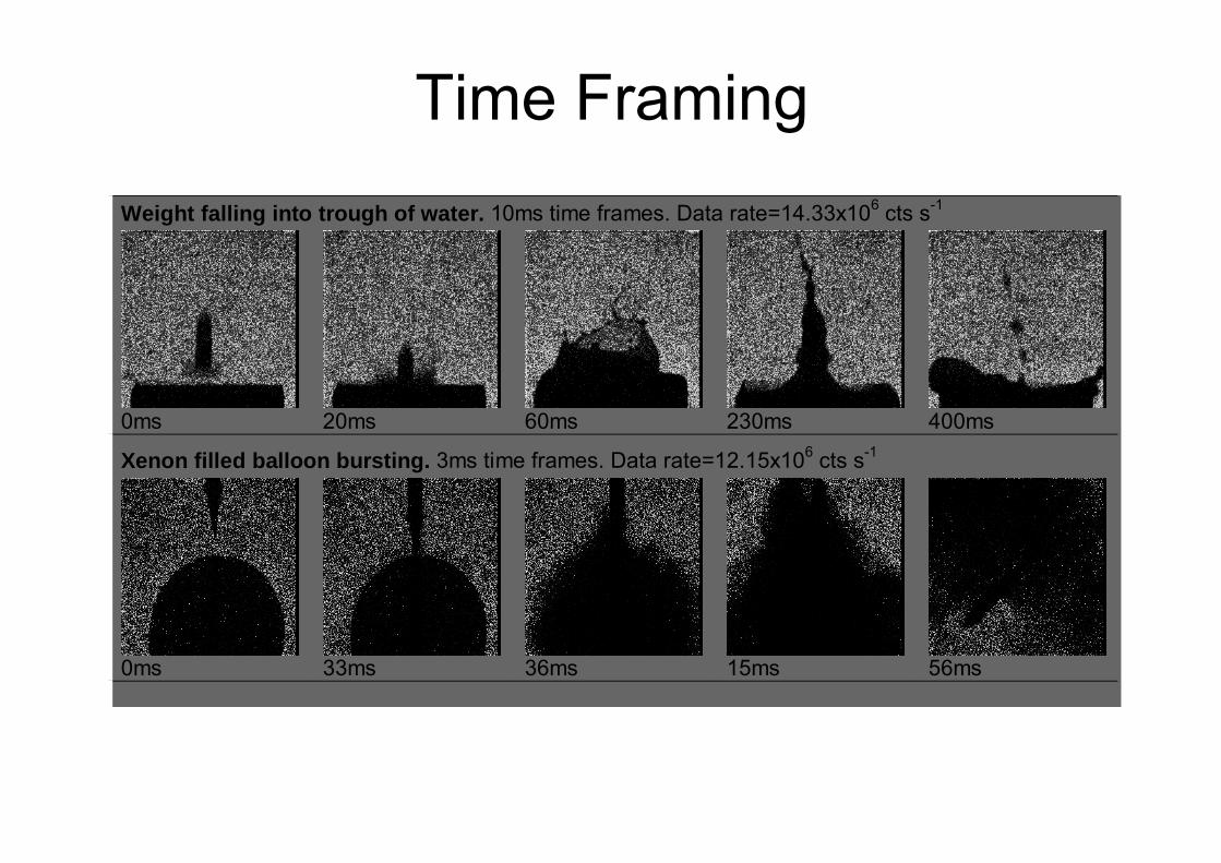
Time FramingWeight falling into trough of water. 10ms time frames. Data rate=14.33x10⁶ cts s-1
0ms 20ms 60ms 230ms 400ms
Xenon filled balloon bursting. 3ms time frames. Data rate=12.15x10⁶ cts s-1
0ms 33ms 36ms 15ms 56ms
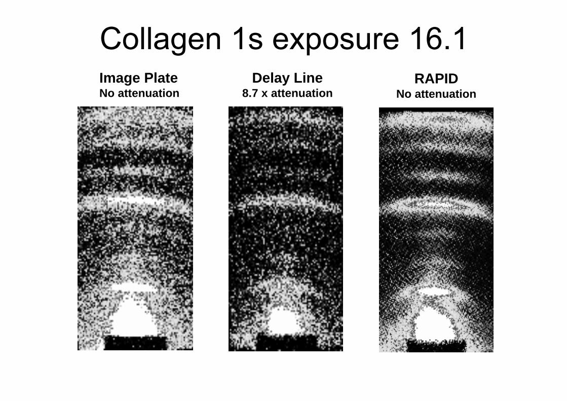
Collagen 1s exposure 16.1RAPID
No attenuationImage PlateNo attenuation
Delay Line8.7 x attenuation
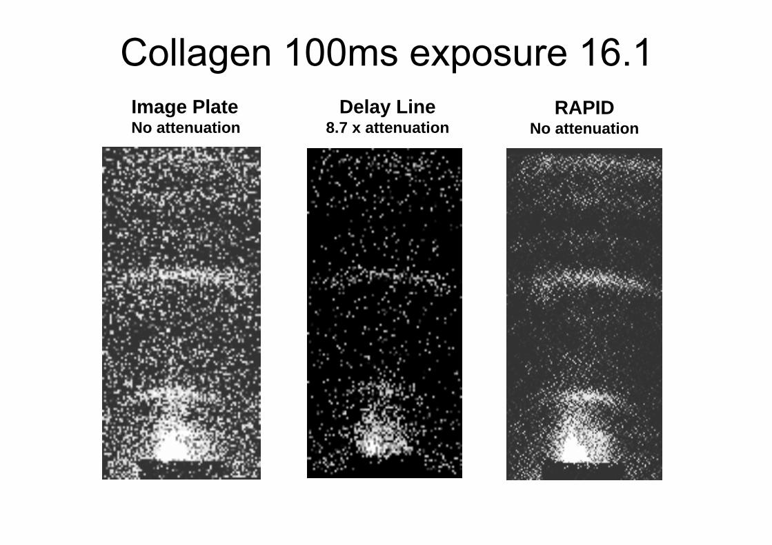
Image PlateNo attenuation
Collagen 100ms exposure 16.1RAPID
No attenuationDelay Line
8.7 x attenuation

Background RemovalBefore After
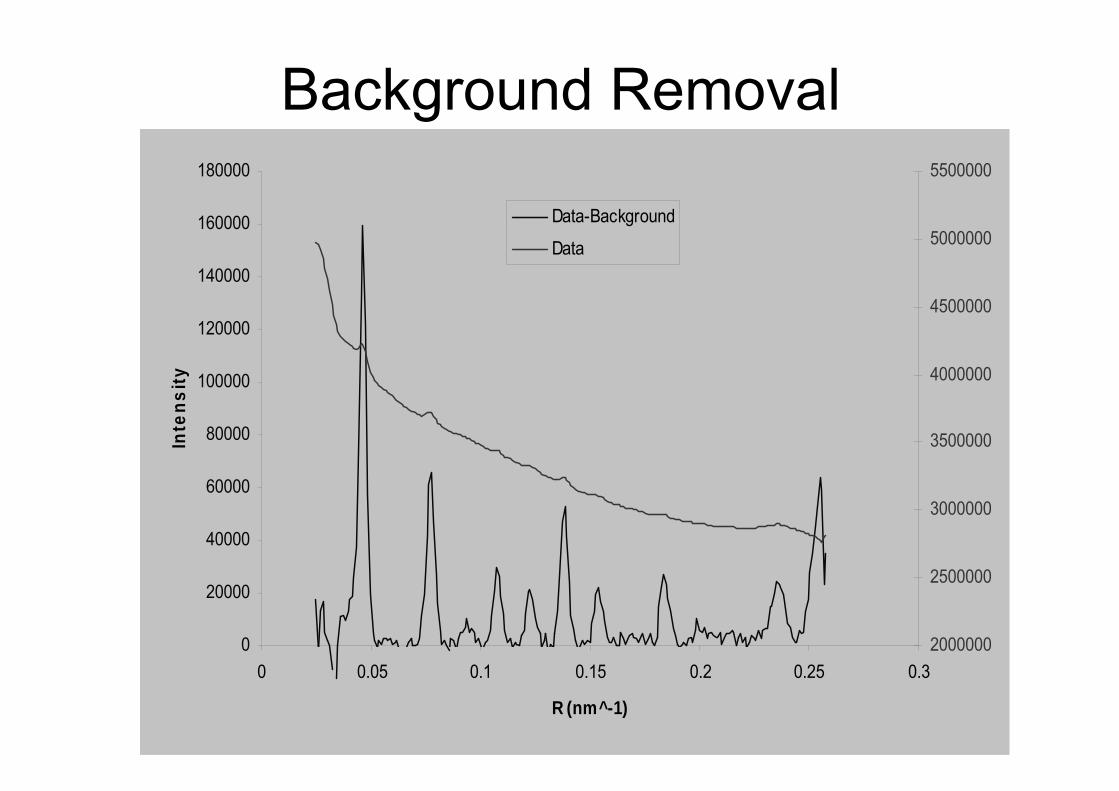
Background Removal
0
20000
40000
60000
80000
100000
120000
140000
160000
180000
0 0.05 0.1 0.15 0.2 0.25 0.3
R (nm^-1)
Inte
nsity
2000000
2500000
3000000
3500000
4000000
4500000
5000000
5500000
Data-Background
Data
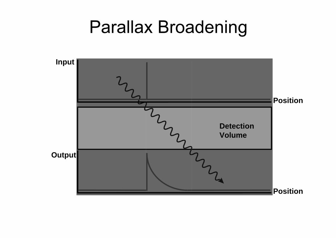
Parallax Broadening
Input
Output
Position
Position
Detection Volume
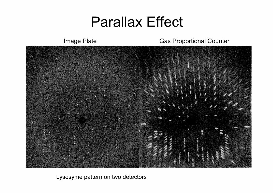
Parallax EffectGas Proportional CounterImage Plate
Lysosyme pattern on two detectors
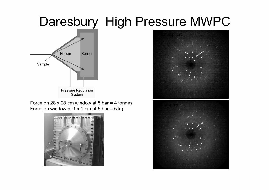
Daresbury High Pressure MWPC
Helium
Pressure RegulationSystem
Xenon
Sample
Force on 28 x 28 cm window at 5 bar = 4 tonnes Force on window of 1 x 1 cm at 5 bar = 5 kg
1 atmosphere
5 atmospheres
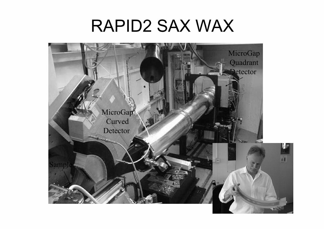
RAPID2 SAX WAXMicroGapQuadrantDetector
MicroGapCurved
Detector
RAPIDelectronics
Sample
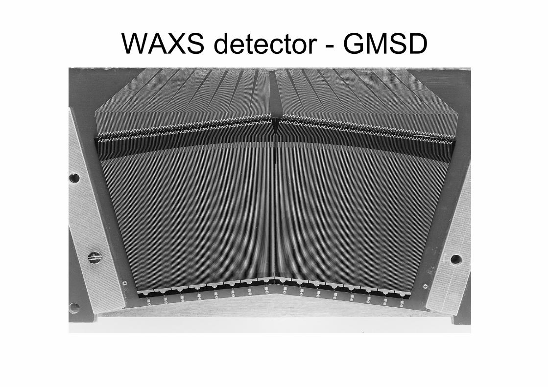
WAXS detector - GMSD
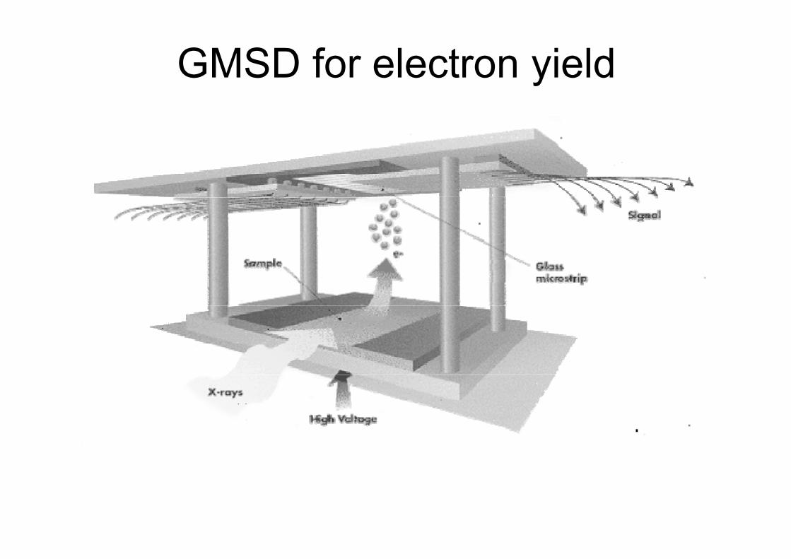
GMSD for electron yield
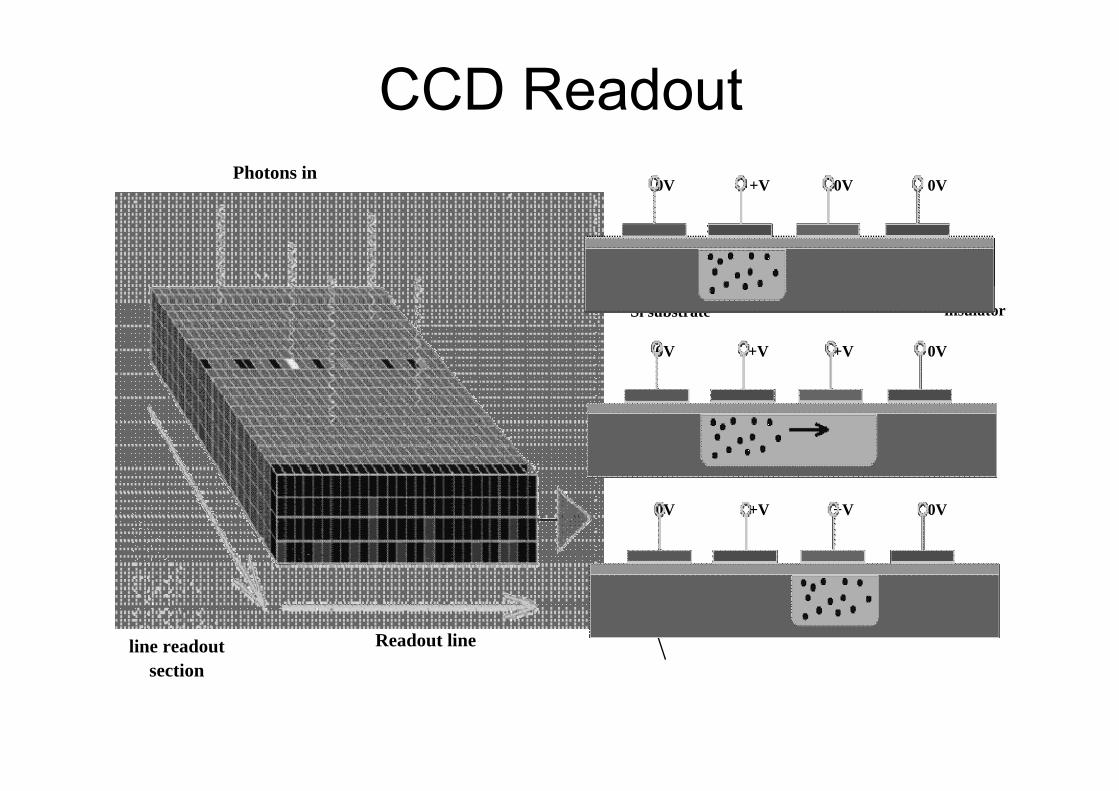
CCD Readout
SiO2
insulatorSi substrate
Stored Charge
0V +V +V 0V
0V +V 0V 0V
0V +V +V 0V
Clock rows into line readout
sectionReadout line
Photons in
CCD Readout
Charge is moved from pixel to pixel by clockingEach pixel has a limited capacitance (well depth) typically 104-105 e-
This limits dynamic range for direct detectionSpeed of clocking is restricted by line capacitance and charge transfer efficiency– Size of CCD restricted by this
Noise can be reduced by coolingAmplifier usually on chip– Heats up that part of chip
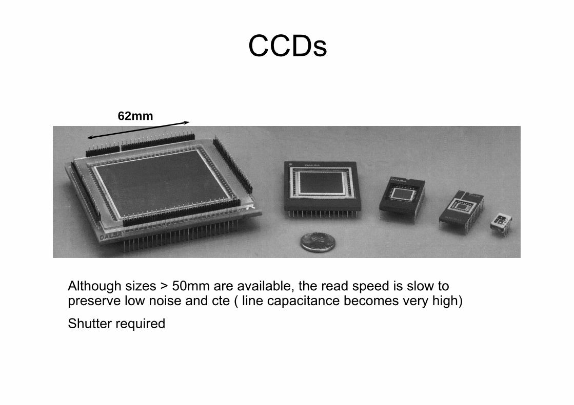
CCDs
Although sizes > 50mm are available, the read speed is slow to preserve low noise and cte ( line capacitance becomes very high)
Shutter required
62mm
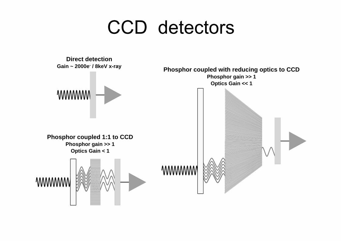
Phosphor coupled with reducing optics to CCDPhosphor gain >> 1
Optics Gain << 1
CCD detectors
Phosphor coupled 1:1 to CCDPhosphor gain >> 1
Optics Gain < 1
Direct detectionGain ~ 2000e- / 8keV x-ray
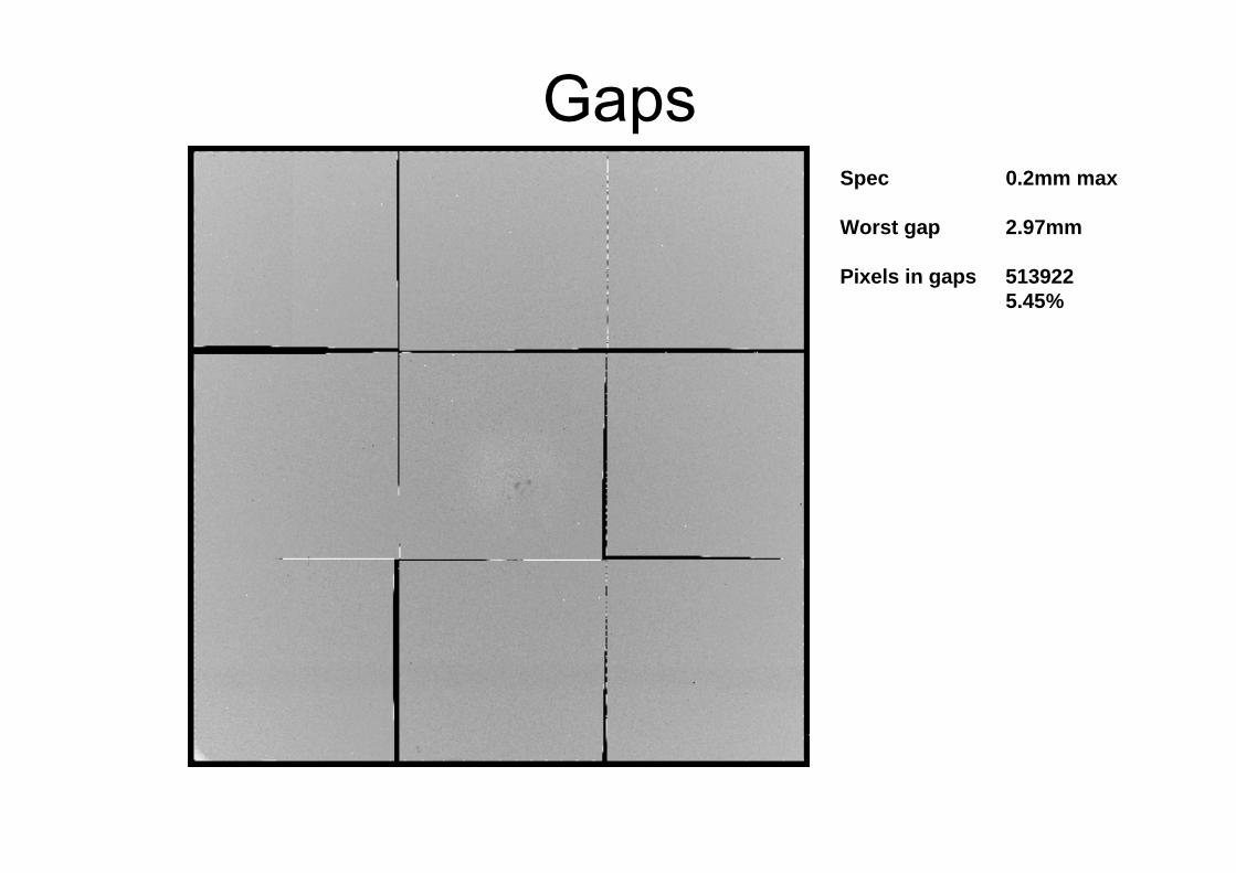
GapsSpec 0.2mm max
Worst gap 2.97mm
Pixels in gaps 5139225.45%
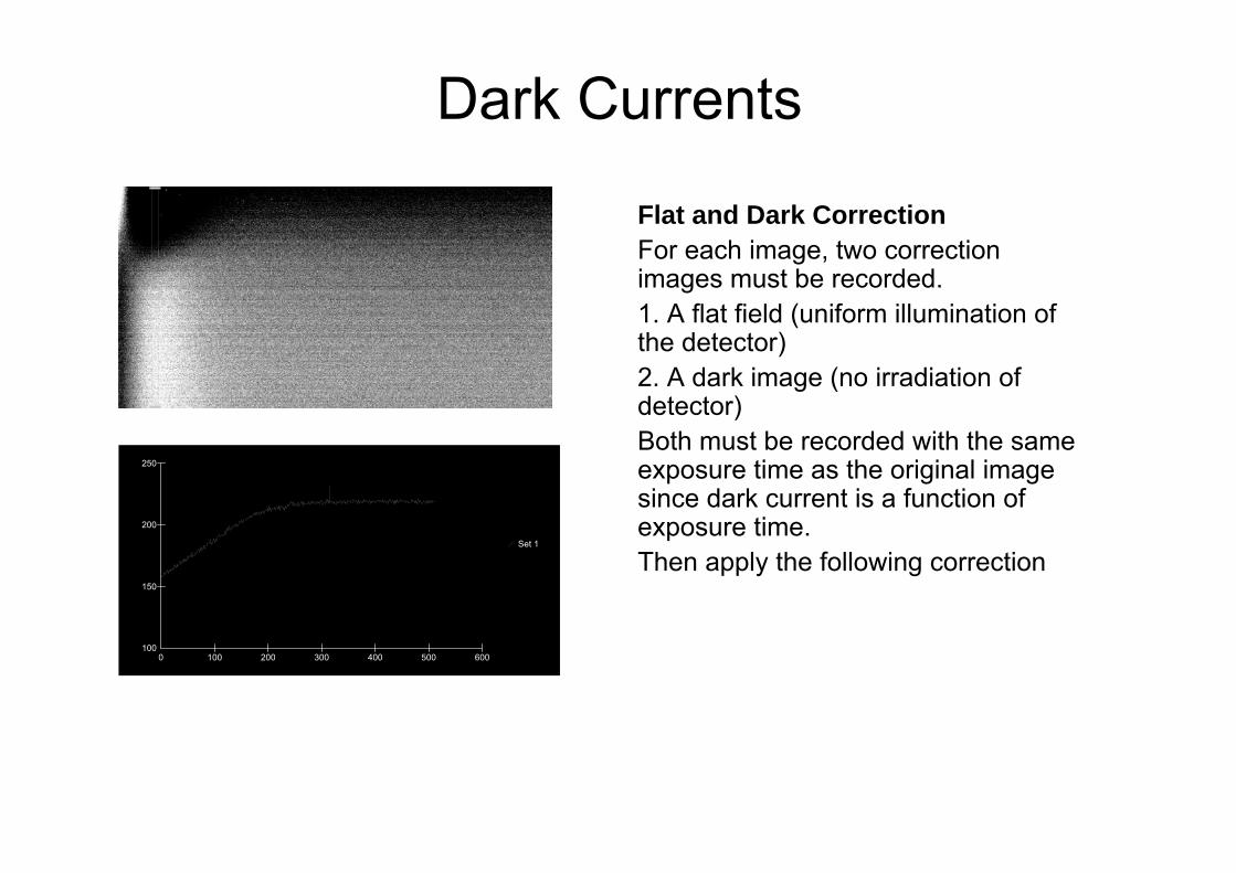
Dark Currents
Flat and Dark CorrectionFor each image, two correction images must be recorded.1. A flat field (uniform illumination of the detector)2. A dark image (no irradiation of detector)Both must be recorded with the same exposure time as the original image since dark current is a function of exposure time.Then apply the following correction
Set 1
100
150
200
250
0 100 200 300 400 500 600( )( )darkflat
darkimageCorrected−−
=
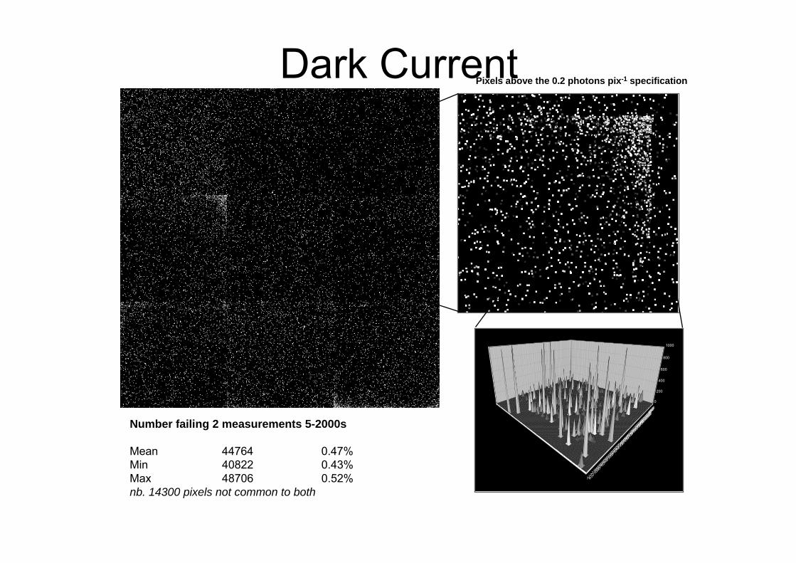
Dark Current
0
200
400
600
800
1000
01234567891011121314151617181920212223242526272829303132333435363738394041424344454647484950515253545556575859606162636465666768697071727374
Pixels above the 0.2 photons pix-1 specification
Number failing 2 measurements 5-2000s
Mean 44764 0.47%Min 40822 0.43%Max 48706 0.52%nb. 14300 pixels not common to both
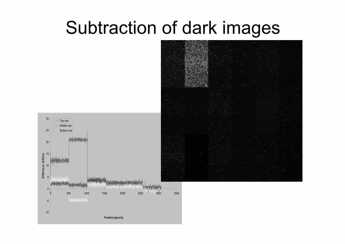
Subtraction of dark images
-10
-5
0
5
10
15
20
25
30
0 500 1000 1500 2000 2500 3000 3500
Position (pixels)
Diffe
renc
e (A
DUs)
Top rowMiddle rowBottom row
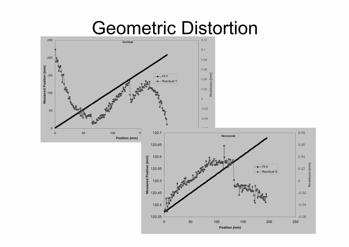
Geometric DistortionVertical
0
50
100
150
200
250
0 50 100 150 200 250
Position (mm)
Mea
sure
d Po
sitio
n (m
m)
-0.06
-0.04
-0.02
0
0.02
0.04
0.06
0.08
0.1
0.12
Resi
dual
s (m
m)
Fit Y
Residual Y
Horizontal
120.35
120.4
120.45
120.5
120.55
120.6
120.65
120.7
0 50 100 150 200 250Position (mm)
Mea
sure
d Po
sitio
n (m
m)
-0.06
-0.04
-0.02
0
0.02
0.04
0.06
0.08
Resi
dual
s (m
m)
Fit X
Residual X
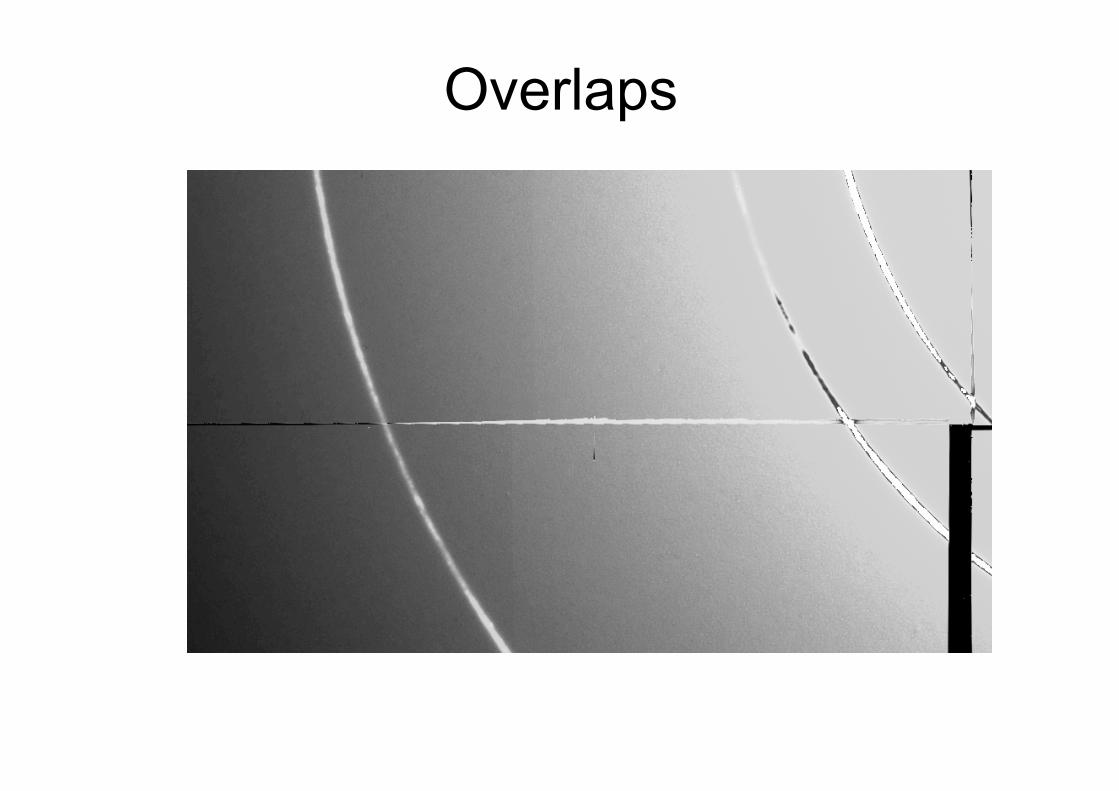
Overlaps
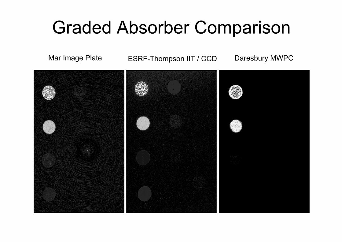
Graded Absorber ComparisonMar Image Plate ESRF-Thompson IIT / CCD Daresbury MWPC

Detector noise level comparison
Position (arb. units)
0 200 400 600 800 1000 1200 1400 1600
Inte
nsity
(pho
tons
/ m
m2 )
10-1
100
101
102
103
104
MWPC Image Plate Intensified CCD
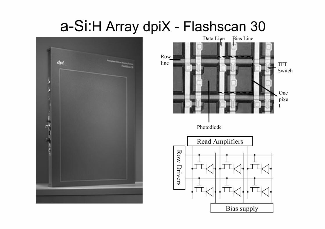
a-Si:H Array dpiX - Flashscan 30
TFT Switch
Bias LineData Line
Photodiode
Row line
One pixel
Read AmplifiersR
ow D
rivers
Bias supply
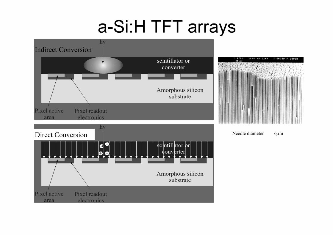
a-Si:H TFT arrays
Amorphous siliconsubstrate
Pixel readoutelectronics
Pixel activearea
hv
scintillator orconverter
Needle diameter 6μm
Indirect Conversion
Amorphous siliconsubstrate
Pixel readoutelectronics
Pixel activearea
hv
scintillator orconverter+ +
Direct Conversion
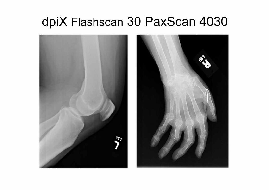
dpiX Flashscan 30 PaxScan 4030
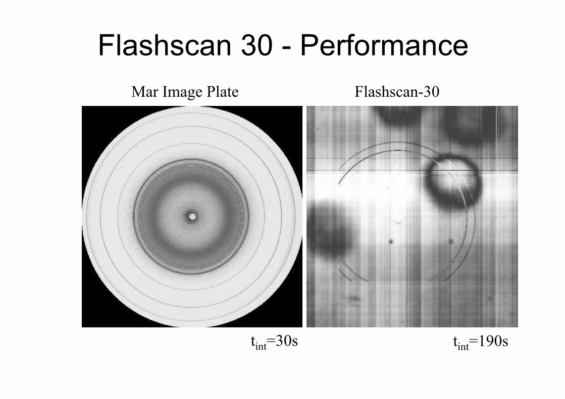
Flashscan 30 - PerformanceMar Image Plate
tint=30s
Flashscan-30
tint=190s
0.10%
1.00%
10.00%
100.00%
0 2 4 6 8 10 12Time (Minutes)
Frac
tion
of in
itial
diff
eren
ce re
mai
ning
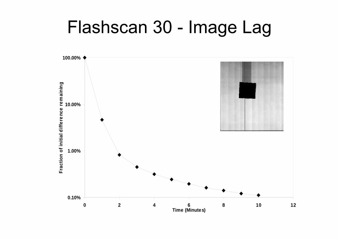
Flashscan 30 - Image Lag
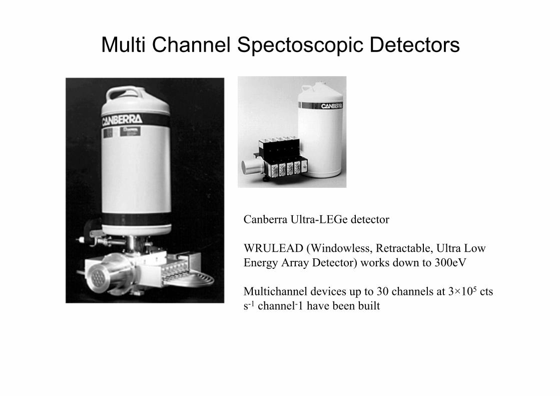
Multi Channel Spectoscopic Detectors
Canberra Ultra-LEGe detector
WRULEAD (Windowless, Retractable, Ultra Low Energy Array Detector) works down to 300eV
Multichannel devices up to 30 channels at 3×10⁵ ctss-1 channel-1 have been built
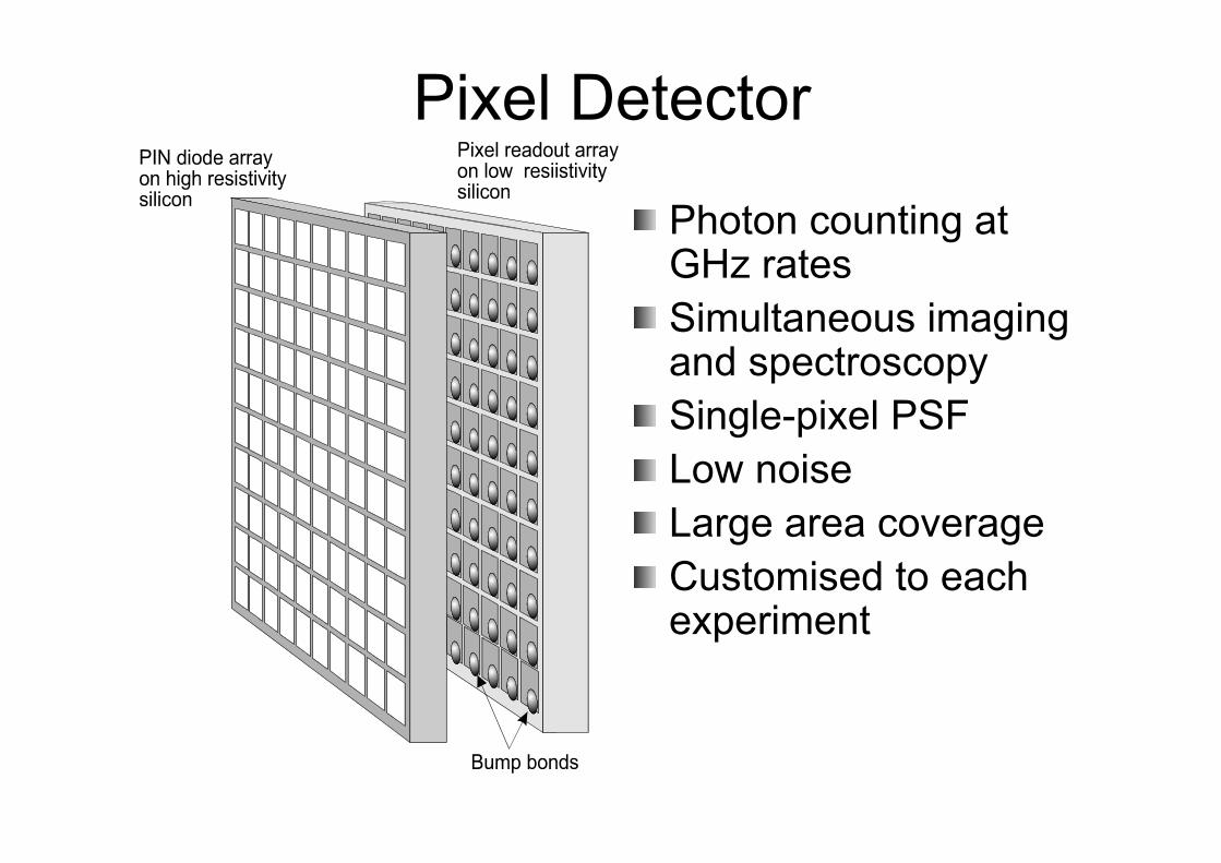
Pixel Detector
Photon counting at GHz ratesSimultaneous imaging and spectroscopySingle-pixel PSF Low noiseLarge area coverageCustomised to each experiment
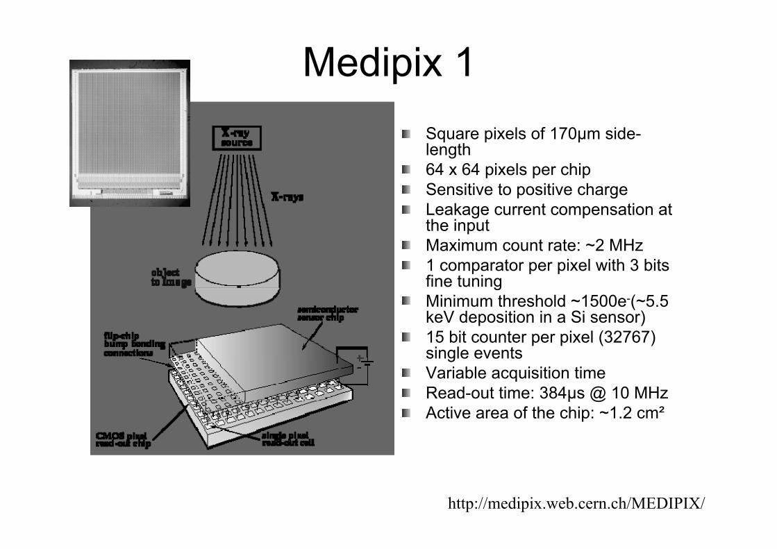
Medipix 1Square pixels of 170µm side-length 64 x 64 pixels per chip Sensitive to positive charge Leakage current compensation at the input Maximum count rate: ~2 MHz 1 comparator per pixel with 3 bits fine tuning Minimum threshold ~1500e-(~5.5 keV deposition in a Si sensor) 15 bit counter per pixel (32767) single events Variable acquisition time Read-out time: 384µs @ 10 MHz Active area of the chip: ~1.2 cm²
http://medipix.web.cern.ch/MEDIPIX/
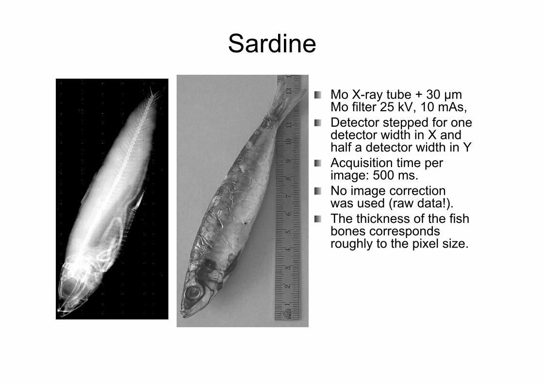
Sardine
Mo X-ray tube + 30 µm Mo filter 25 kV, 10 mAs, Detector stepped for one detector width in X and half a detector width in YAcquisition time per image: 500 ms. No image correction was used (raw data!). The thickness of the fish bones corresponds roughly to the pixel size.
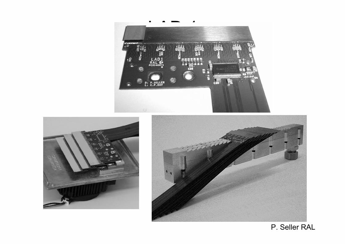
LAD 1
P. Seller RAL
Detector GroupPaul Scherrer Institut
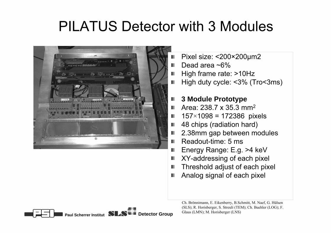
PILATUS Detector with 3 Modules
Pixel size: <200×200µm2Dead area ~6%High frame rate: >10HzHigh duty cycle: <3% (Tro<3ms)
3 Module PrototypeArea: 238.7 x 35.3 mm2
157×1098 = 172386 pixels 48 chips (radiation hard)2.38mm gap between modulesReadout-time: 5 msEnergy Range: E.g. >4 keVXY-addressing of each pixelThreshold adjust of each pixelAnalog signal of each pixel
Ch. Brönnimann, E. Eikenberry, B.Schmitt, M. Naef, G. Hülsen (SLS); R. Horisberger, S. Streuli (TEM); Ch. Buehler (LOG); F. Glaus (LMN); M. Horisberger (LNS)
Detector GroupPaul Scherrer Institut
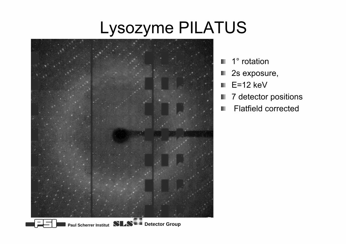
Lysozyme PILATUS
1° rotation2s exposure, E=12 keV 7 detector positionsFlatfield corrected
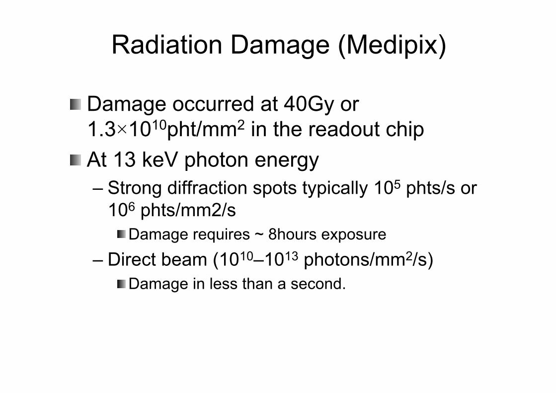
Radiation Damage (Medipix)
Damage occurred at 40Gy or 1.3×10¹⁰pht/mm2 in the readout chipAt 13 keV photon energy– Strong diffraction spots typically 105 phts/s or
106 phts/mm2/sDamage requires ~ 8hours exposure
– Direct beam (1010–1013 photons/mm2/s) Damage in less than a second.
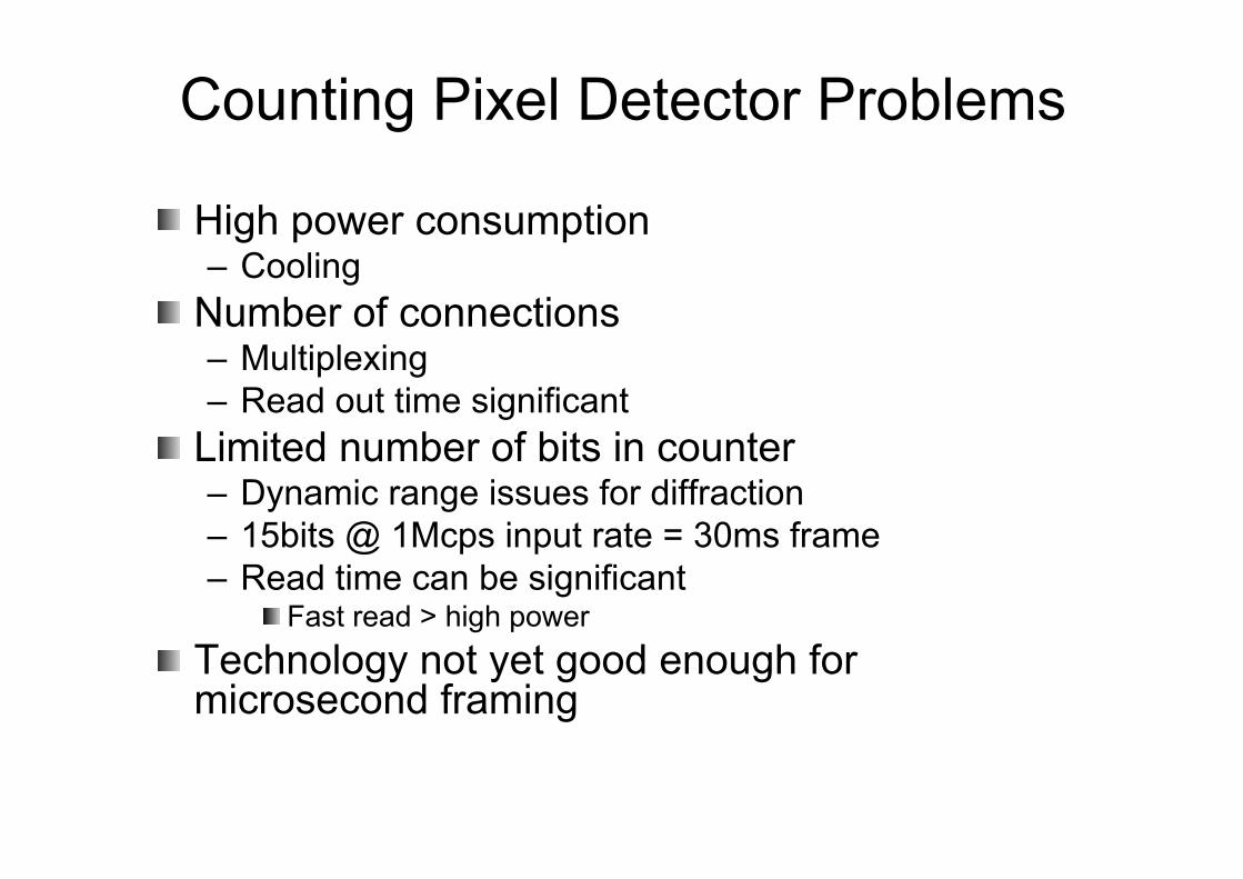
Counting Pixel Detector Problems
High power consumption– Cooling
Number of connections– Multiplexing– Read out time significant
Limited number of bits in counter– Dynamic range issues for diffraction– 15bits @ 1Mcps input rate = 30ms frame– Read time can be significant
Fast read > high powerTechnology not yet good enough for microsecond framing
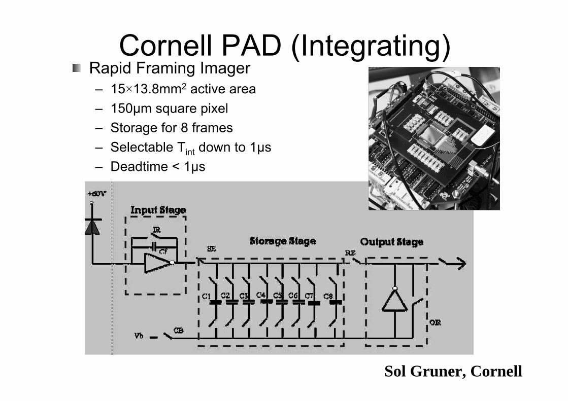
Cornell PAD (Integrating)Rapid Framing Imager– 15×13.8mm2 active area– 150µm square pixel– Storage for 8 frames– Selectable Tint down to 1µs– Deadtime < 1µs
Sol Gruner, Cornell
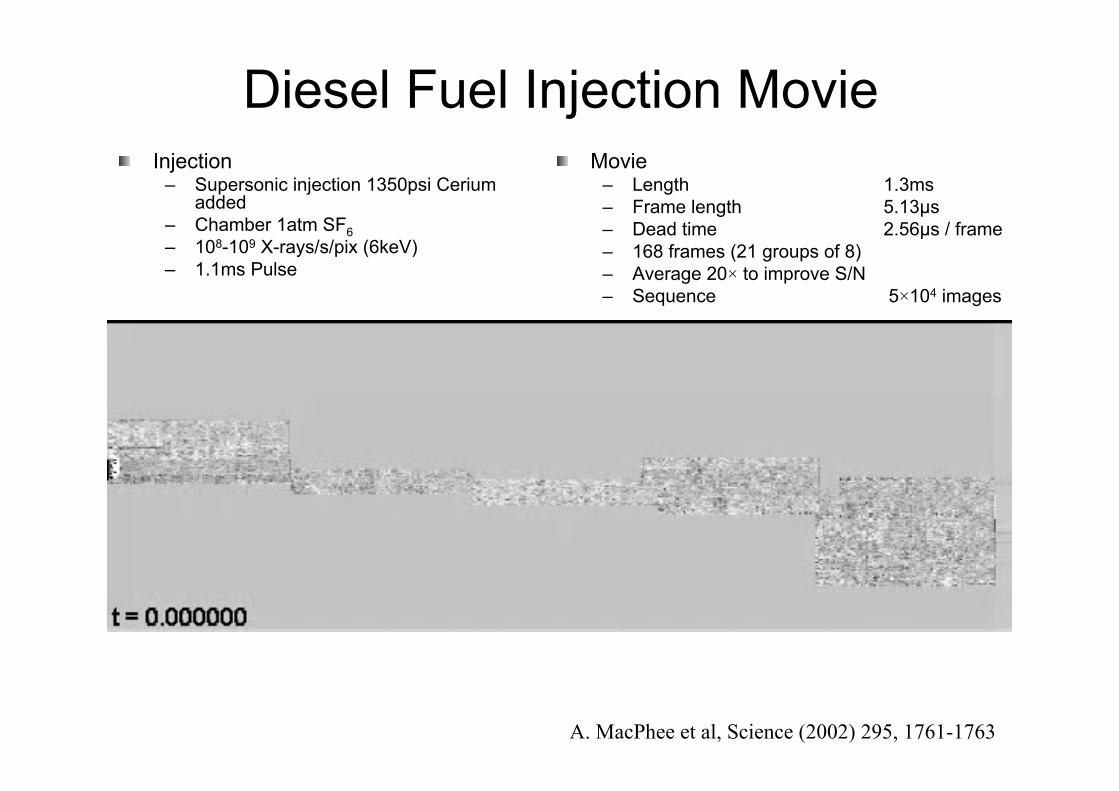
Diesel Fuel Injection MovieInjection
– Supersonic injection 1350psi Cerium added
– Chamber 1atm SF6– 108-109 X-rays/s/pix (6keV)– 1.1ms Pulse
A. MacPhee et al, Science (2002) 295, 1761-1763
Movie– Length 1.3ms– Frame length 5.13µs– Dead time 2.56µs / frame– 168 frames (21 groups of 8)– Average 20× to improve S/N– Sequence 5×10⁴ images
Pixel Detectors: The Problems
Large silicon fab requirementsA lot of infrastructure requiredRadiation damageLong iteration timesPoor stopping power of siliconCounting and fast framing not yet possibleExpensive NRE
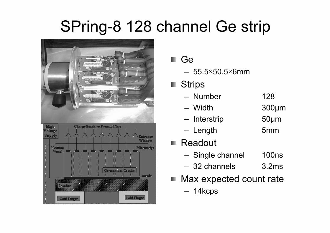
SPring-8 128 channel Ge strip
Ge– 55.5×50.5×6mm
Strips– Number 128– Width 300µm– Interstrip 50µm– Length 5mm
Readout– Single channel 100ns– 32 channels 3.2ms
Max expected count rate– 14kcps
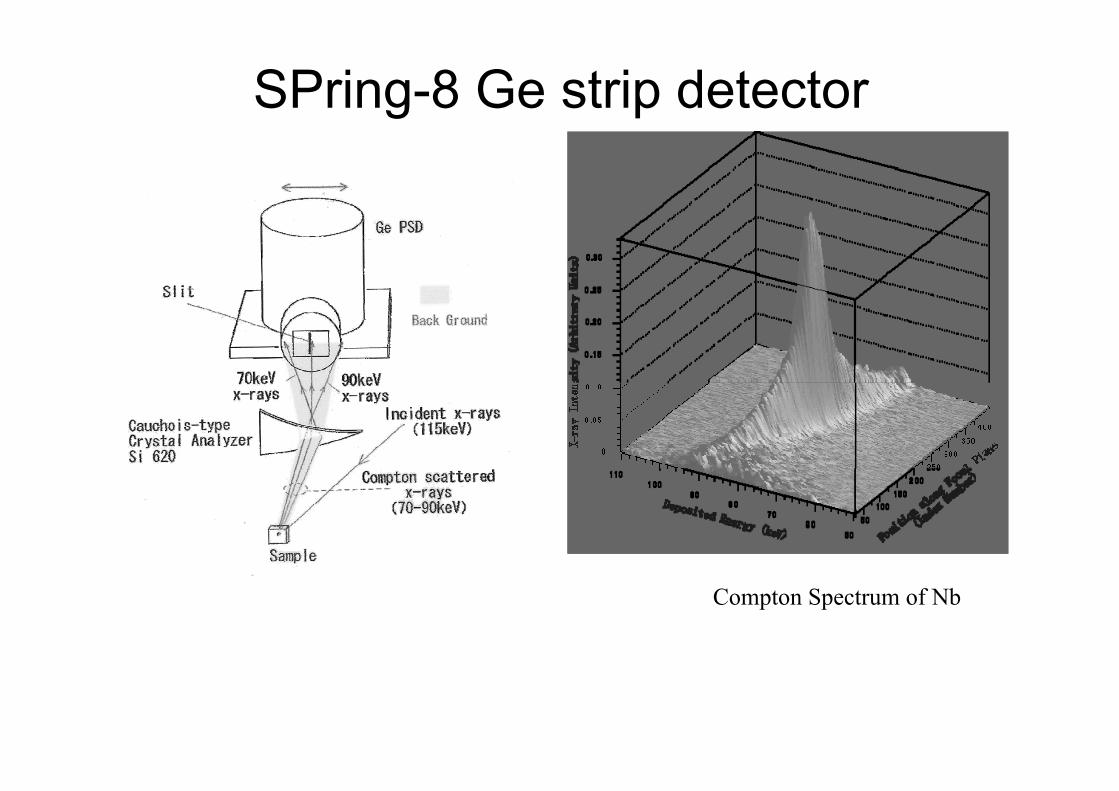
SPring-8 Ge strip detector
Compton Spectrum of Nb
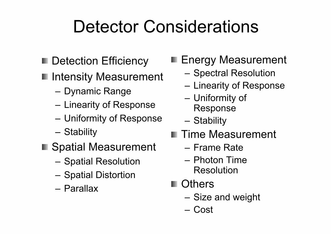
Detector Considerations
Detection EfficiencyIntensity Measurement– Dynamic Range– Linearity of Response– Uniformity of Response– Stability
Spatial Measurement– Spatial Resolution– Spatial Distortion– Parallax
Energy Measurement– Spectral Resolution– Linearity of Response– Uniformity of
Response– Stability
Time Measurement– Frame Rate– Photon Time
ResolutionOthers– Size and weight– Cost
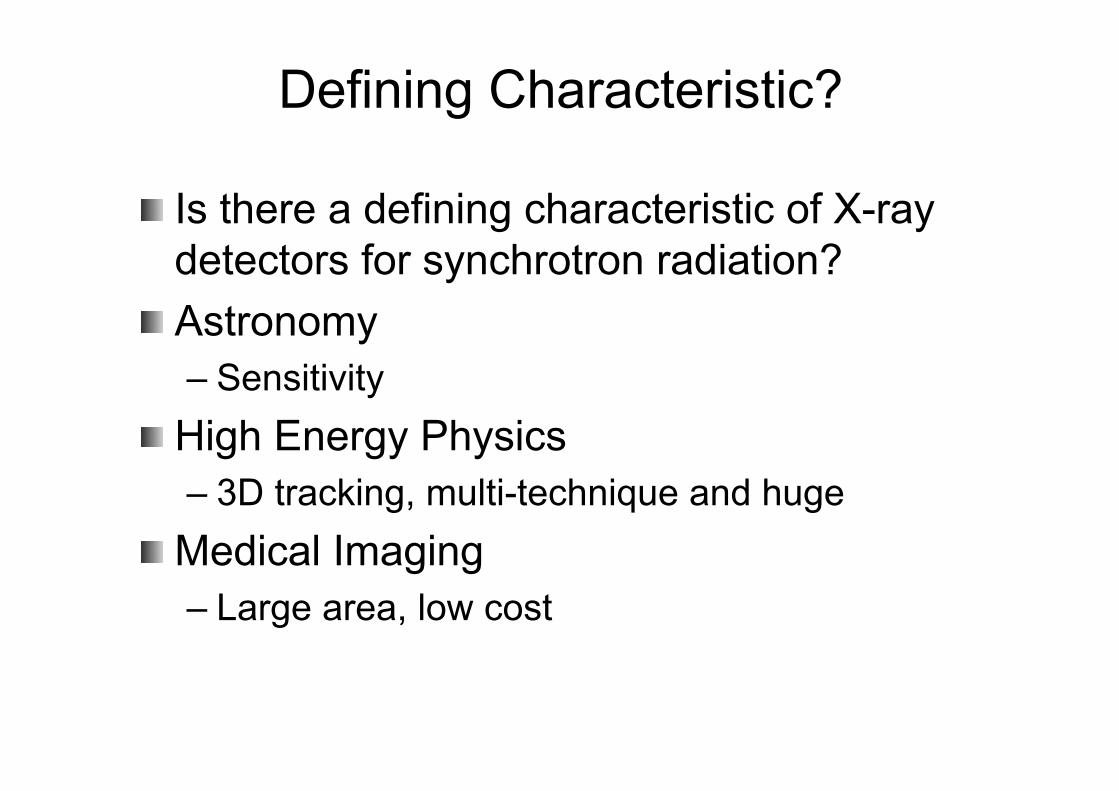
Defining Characteristic?
Is there a defining characteristic of X-ray detectors for synchrotron radiation?Astronomy– Sensitivity
High Energy Physics– 3D tracking, multi-technique and huge
Medical Imaging– Large area, low cost
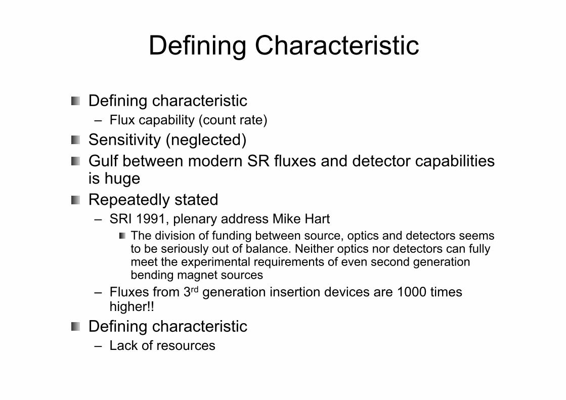
Defining Characteristic
Defining characteristic – Flux capability (count rate)
Sensitivity (neglected)Gulf between modern SR fluxes and detector capabilities is hugeRepeatedly stated– SRI 1991, plenary address Mike Hart
The division of funding between source, optics and detectors seems to be seriously out of balance. Neither optics nor detectors can fully meet the experimental requirements of even second generation bending magnet sources
– Fluxes from 3rd generation insertion devices are 1000 times higher!!
Defining characteristic– Lack of resources
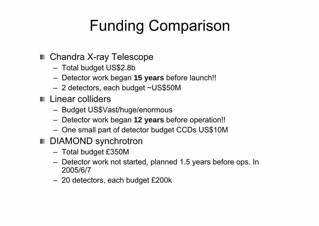
Funding Comparison
Chandra X-ray Telescope– Total budget US$2.8b– Detector work began 15 years before launch!!– 2 detectors, each budget ~US$50M
Linear colliders– Budget US$Vast/huge/enormous– Detector work began 12 years before operation!!– One small part of detector budget CCDs US$10M
DIAMOND synchrotron– Total budget £350M– Detector work not started, planned 1.5 years before ops. In
2005/6/7– 20 detectors, each budget £200k
Tortoise and Hare?
Accelerators currently 1013-1014 photons to sampleNew machines e.g. LCLS, TESLA– 1025 photons to sample!!!
Detectors– Currently 107-108
– In 10 years…………Hare shows no sign of slowing downTortoise is not catching up
References
Delaney CFG and Finch EC– Radiation detectors. Physical Principles and
Applications, Clarendon Press, Oxford 1992, ISBN 0 19 853923 1
Knoll GE– Radiation Detection and Measurement, John Wiley
and Sons 3rd edition, 2000Proceedings of the 7th International Conference on position sensitive detectors– Nuclear Instruments and Methods in Physics
Research A573 (2007)IEEE Nuclear Science Symposia