Embed Size (px)
Citation preview

Design Space Exploration OfField Programmable Counter Arrays And Their Integration With FPGAs
Master Diploma WorkKTH/ICT/ECS-2008-21
Student: Seyed Hosein Attarzadeh NiakiProject Supervisors: Philip Brisk, Paolo Ienne (EPFL)Project Adviser: Axel Jantsch (KTH)


i
Abstract
Field Programmable Counter Arrays (FPCAs) have been recently introduced to close the gap between FPGA and ASICs for arithmetic dominated applications. FPCAs are reconfigurable lattices that can be embedded into FPGAs to efficiently compute the result of multi-operand additions.
The first contribution of this work is a Design Space Exploration (DSE) of the FPCAs and the identification of trade-offs between different parameters which describe them. Methods for analyzing and pruning the design space are proposed to enable a smart exploration. Finally, a set of best performing architectures in terms of area and delay is determined.
Secondly, a study of possible integration schemes to build a hybrid FPGA/FPCA chip is performed. The goal is to find a solution with optimal usage of on-chip silicon area. The advantages and disadvantages of each solution are studied and a new integration solution based on properties of FPCAs is suggested. A VLSI implementation proves the applicability of the proposed solutions.

ii
Acknowledgments
It has been a wonderful experience to study my master degree in Royal Institute
of Technology (KTH) and to do my thesis work in Federal Polytechnical University of
Lausanne (EPFL).
First of all, I wish to thank my academic supervisor, Dr. Philip Brisk, for his
guidance, technical and moral support that he provided during my thesis work. I'm
extremely grateful for his kind consideration. The technical advices which I received
from my official supervisor, professor Paolo Ienne, and my advisor, professor Axel
Jantsch, were really helpful. Also, there were so many people that shared their
experience and knowledge with me to improve the quality of this work, among them:
Alessandro Cevrero, Frank Gürkaynak and Chrysostomos Nicopoulos.
I should also note that I am always thankful to my parents and will never forget
that they never refused their support and encouragement a single moment in my life.
iii
Table of ContentsIntroduction................................................................................................................................................1 Chapter 1:Field Programmable Gate Arrays...............................................................................................................2
1.1 Basic Architecture..........................................................................................................................2 1.2 Logic Blocks..................................................................................................................................2 1.3 FPGA Routing Architecture...........................................................................................................5
1.3.1 Connection Blocks..................................................................................................................6 1.3.2 Switch Blocks.........................................................................................................................8
1.4 Circuit Level Design......................................................................................................................9 1.4.1 Programming Technology......................................................................................................9 1.4.2 Directional and Single Driver Wires....................................................................................10
1.5 Heterogeneity in FPGAs..............................................................................................................11 1.6 Design Methodology and Tools...................................................................................................12 1.7 Case Study: Altera Stratix II FPGA Architecture.........................................................................12
1.7.1 Adaptive Logic Module and Logic Array Block..................................................................13 1.7.2 The Routing Network...........................................................................................................15
Chapter 2:Field Programmable Counter Arrays.......................................................................................................19
2.1 Arithmetic Primitives...................................................................................................................19 2.1.1 Number Representation and Dot Notation...........................................................................19 2.1.2 Serial Multi-Operand Addition.............................................................................................20 2.1.3 Adder Trees...........................................................................................................................20 2.1.4 Carry Save Adders................................................................................................................21 2.1.5 Compressor Trees.................................................................................................................21 2.1.6 Parallel Counters..................................................................................................................21 2.1.7 Generalized Parallel Counters..............................................................................................23
2.2 FPCA CSlice Architecture............................................................................................................23 2.3 Multi-FPCA Configurations.........................................................................................................26 2.4 Mapping Compressor Trees onto FPCAs.....................................................................................27
Chapter 3:Design Space Exploration of FPCAs.......................................................................................................28
3.1 Why Design Space Exploration?..................................................................................................28 3.2 CSlice Characterization................................................................................................................28 3.3 FPCA Model.................................................................................................................................29
3.3.1 Generic HDL for FPCA........................................................................................................29 3.3.2 Model Verification................................................................................................................30
3.4 Mapping Heuristic........................................................................................................................30 3.5 Analysis of the Design Space.......................................................................................................30
3.5.1 Effect of First Level Counter Size........................................................................................31 3.5.2 Effect of Maximum Output Rank.........................................................................................31 3.5.3 Effect of Generalized Parallel Counter Configuration.........................................................31 3.5.4 Utilization Metrics................................................................................................................31

iv
3.6 Experimental Results....................................................................................................................32 3.6.1 Tools and Methodology........................................................................................................32 3.6.2 Benchmarks..........................................................................................................................33 3.6.3 Results..................................................................................................................................34
Chapter 4:FPCA Integration with FPGAs................................................................................................................43
4.1 The Problem.................................................................................................................................43 4.2 Related Works..............................................................................................................................43 4.3 FPCA Integration Scenarios.........................................................................................................47
4.3.1 Area Based Integration.........................................................................................................47 4.3.2 Pin-Demand Based Integration.............................................................................................48 4.3.3 Shadow Clusters Based Integration......................................................................................49 4.3.4 Shadow Cluster - Extra Usage-Based Integration................................................................50
4.4 Modeling and Implementation.....................................................................................................51Summary and Conclusions......................................................................................................................54Future Work.............................................................................................................................................54References................................................................................................................................................55 Appendix A :Design Space Exploration Platform...................................................................................59
A.1 FPCA HDL Model.......................................................................................................................59 A.2 FPCA Generator Module.............................................................................................................65 A.3 Mapping Module.........................................................................................................................66 A.4 Exploration Module.....................................................................................................................66
Appendix B :FPGA Architecture Generator Platform............................................................................67 B.1 Switch Generator Module............................................................................................................67 B.2 IIB Generator Module.................................................................................................................68 B.3 Basic FPGA Tile Generator Module............................................................................................68 B.4 Basic FPCA Tile Generator Module............................................................................................68 B.5 Shadow Tile Generators...............................................................................................................69

v
Illustration IndexFigure 1.1: Island-style FPGA architecture...............................................................................................3Figure 1.2: Basic Logic Element and Clustered Logic Block...................................................................4Figure 1.3: 6,2 Shared LUT mask logic element.......................................................................................5Figure 1.4: General routing architecture of island-style FPGA.................................................................6Figure 1.5: Detailed routing architecture of island-style FPGA................................................................7Figure 1.6: Input Interconnection Block....................................................................................................8Figure 1.7: Proposed IIB............................................................................................................................8Figure 1.8: Construction of proposed IIB..................................................................................................9Figure 1.9: Three FPGA switch blocks with Fs=3.....................................................................................9Figure 1.10: Circuit level design of SRAM based FPGAs......................................................................10Figure 1.11: Possible circuit level implementation of routing switches..................................................11Figure 1.12: Directional and bidirectional implementation of disjoint switch box ................................12Figure 1.13: Merging switch blocks and output connection blocks into a new routing block in single driver wiring.............................................................................................................................................12Figure 1.14: General Stratix II architecture.............................................................................................14Figure 1.15: Adaptive Logic Module in Stratix II device........................................................................15Figure 1.16: Logic Array Block...............................................................................................................17Figure 1.17: Driving vertical lines in Stratix II routing network.............................................................18Figure 1.18: Driving horizontal lines in Stratix II routing network.........................................................19Figure 1.19: Routing network connections to LABs...............................................................................19Figure 2.1: Dot notation representation of a 4x4 multiplication..............................................................23Figure 2.2: Serial addition........................................................................................................................23Figure 2.3: A binary adder tree................................................................................................................23Figure 2.4: Building a carry-save adder out of a ripple carry adder........................................................24Figure 2.5: A CSA based approach to multi-operand addition................................................................25Figure 2.6: Construction of a 10:4 parallel counter.................................................................................25Figure 2.7: Dot notation representation of examples of GPCs................................................................26Figure 2.8: Using parallel counters to reduce a compressor tree.............................................................27Figure 2.9: CSlice interconnections.........................................................................................................27Figure 2.10: A GPC, built by adding a GPCCC to the input of a parallel counter..................................28Figure 2.11: Example of a CSlice used in this work with MORC=1 and FCS=31:5..............................29Figure 2.12: Multi-FPCA configurations (a) Horizontal (b) Vertical......................................................30Figure 2.13: Pseudo-code used for Mapping an input bit pattern to FPCA.............................................30Figure 3.1: Functional operation of the DSE tool....................................................................................36Figure 3.2: DSE results for mul5x5 benchmark with FCS=15,31...........................................................38Figure 3.3: DSE results for mul18x18 and add16x16 benchmarks with FCS=31..................................39Figure 3.4: DSE results for add8x32 benchmark with FCS=15,31........................................................40Figure 3.5: DSE results for SAD benchmark with FCS=15,31..............................................................41Figure 3.6: DSE results for mul36x18 and FIR benchmarks with FCS=31............................................42Figure 3.7: Average area/delay results on different GPCCC architectures for FCS=15,31.....................43Figure 3.8: The correlation between Uin and Uout values......................................................................44Figure 3.9: Best average utilization values for different architectures....................................................45Figure 4.1: An example of integrating RAMs as hard blocks..................................................................47Figure 4.2: Example of memory/logic interconnect block......................................................................48

vi
Figure 4.3: Expansion of the gridded routing fabric over the embedded block......................................48Figure 4.4: Illustration of shadow cluster concept...................................................................................50Figure 4.5: Area-based integration of FPCAs..........................................................................................51Figure 4.6: Pin-demand-based integration of FPCAs..............................................................................52Figure 4.7: Shadow cluster based integration of FPCAs.........................................................................53Figure 4.8: Shadow cluster - extra usage based integration.....................................................................54Figure 4.9: Block diagram of the baseline FPGA tile used for implementation ....................................55Figure 4.10: Proof of concept layout of baseline FPGA tile....................................................................56Figure 4.11: Alignment of pins for tile-ability of the design...................................................................56

vii
Index of TablesTable 1.1: Routing resources in Stratix II architecture............................................................................18Table 3.1: Benchmark circuits used for DSE...........................................................................................34Table 4.1: Intra-cluster design of LAB and DSP tiles..............................................................................46


1
IntroductionField Programmable Gate Arrays (FPGAs) are prefabricated electronic devices which can be
configured to represent any desired hardware functionality. Compared to Application Specific Integrated Circuits (ASICs), FPGAs can be reconfigured as the application evolves during its design and updated designs can be loaded onto the device even after it has been deployed. The EDA tools and fabrication costs for the first instance of an FPGA ranges from tens to a few thousand dollars, but will rise to hundreds of thousands or millions Dollars for ASICs. The cost of reconfigurability, however, is non-trivial; a recent study by Kuon and Rose [1] on a set of benchmarks shows that the circuits which are implemented on FPGAs have on average 35x larger area, are 3x to 4x slower, and consume 14x more power than their ASIC counterparts. The usage of hard blocks and IP cores reduces this gap, but FPGAs still demonstrate lower performance metrics, especially for arithmetic dominated applications.
Field Programmable Counter Arrays (FPCAs) were introduced by Brisk et al. [2] to help close this gap by accelerating multi-operand additions – which are kernels of many arithmetic applications. The contribution of this work can be divided in two parts:
● A design space exploration of FPCAs, which analyzes different architectural parameters of the FPCAs and their corellations. The goal is to develop methods to identify the optimal FPCA architectures for a set of representative applications.
● Integration of FPCA blocks into existing FPGAs: configurable routing fabrics for FPGAs are studied and integration strategies are proposed to permit an efficient combined FPGA/FPCA lattice.
The rest of this report is organized as follows: The first two chapters provide the reader with a background needed for understanding the contribution of this work. Chapter 1 provides an overview of the FPGA architecture using the architecture of a commercial FPGA as an example. Chapter 2 summerizes prior arithmetic primitives and introduces the FPCA. The design space exploration methodology and a description of the developed tools for this purpose are described in chapter 3. Chapter 4 describes the work done on integrating of FPCAs into FPGAs. Finally, the implementation and results are presented along with a summary and conclusion.

Chapter 1:Field Programmable Gate Arrays 2
Chapter 1:Field Programmable Gate Arrays
This chapter is an introduction to the FPGA architecture. The configurable logic elements of typical FPGAs and the routing architecture used to interconnect them are discussed. An example of a commercial FPGA is presented and a typical FPGA development methodology based on the extensively-used academic VPR CAD Flow is described.
1.1 Basic ArchitectureMost of the today's FPGAs are categorized as island-style FPGAs. An island-style FPGA is a
two dimensional array of logic blocks surrounded by I/O cells on its sides. These logic blocks and I/O cells are all interconnected using a programmable routing architecture. In order to improve the performance of FPGAs, most of the commercial FPGAs also include hard blocks with fixed functionality which offer faster, more compact implementations of hardware functions than synthesis on the general logic of an FPGA. Example of such hard blocks are block RAMs and multipliers. Figure 1.1 illustrates such an architecture.
1.2 Logic BlocksLookup-Tables (LUTs) can be used to store truth table implementations of logic functions. By
storing the proper bits in the LUTs, various combinational logic functions could be implemented. To be able to implement sequential circuits like FSMs, a register is connected to the output of LUTs. This structures which is shown in figure 1.2a is called a Logic Element (LE) or Basic Logic Element (BLE). Previously, it was is shown that 4-input LUTs give the best Area-Delay compromise in FPGAs [3]. Today's FPGAs like Virtex 5 and Altera Stratix II/III/IV use 6-LUTS instead.

Chapter 1:Field Programmable Gate Arrays 3
Figure 1.1: Island-style FPGA architecture[37]
Figure 1.2: Basic Logic Element and Clustered Logic Block[18]

Chapter 1:Field Programmable Gate Arrays 4
In early FPGAs, a routing fabric routed the signals to/from blocks of containing a single BLE; however, it was realized that such an approach is not area-efficient. Instead, a set of BLEs are packed into a Configurable Logic Block (CLB) or Logic Array Block (LAB) and signals are routed between these blocks in the routing network. A programmable intra-cluster routing routes the signals from the inputs of the CLBs to the inputs of BLEs and also feeds back the outputs of the BLEs to their inputs. Since BLEs in a CLB share their inputs, fewer signals can be fed to the cluster, resulting in a smaller routing network. A CLB together with its local interconnections is depicted in figure 1.2b.
Commercial FPGAs also include extra features such as carry chains and register chains. Recently, fracturable LUTs have been suggested as a replacement for simple LUTs in BLEs. The Altera Stratix II and subsequent devices in this family use Adaptive Logic Modules (ALMs) which include a fracturable LUT. Figure 1.3 is a simplified version of a fracturable 6-LUT used in these devices. This structured is called 6,2 shared LUT mask logic element. It is basically a 6-LUT with two additional inputs and can be configured to implement a single 6-input (or a sunset of 7-input) logic function or different combinations of two logic functions with shared inputs.
Figure 1.3: 6,2 Shared LUT mask logic element[20]

Chapter 1:Field Programmable Gate Arrays 5
1.3 FPGA Routing ArchitectureThe main duty of the routing network is to route signals between IO blocks, BLEs and other
hard blocks on the chip (if any). It is very important for a manufacturer to design the network in such a way that the routing doesn't fail because of the lack of interconnection resources. Such a level of connectivity is usually achieved by devoting a considerable amount of silicon area to the routing network. Almost 80 percent of today's FPGAs on-chip area is occupied by routing resources [4].
The problem of designing routing architecture for FPGAs is usually studied in two parts. The global routing architecture design, questions about the positioning and alignment of routing wires relative to the logic blocks, the number of wires in the channels, how they are interconnected to each other and to the logic blocks from a macroscopic point of view. In detailed routing architecture design, the focus is on exact length of wires, the exact number and place of the switches connecting the wires together and to the logic block pins, and whether the wires are driven from a single source or they have multiple drivers.
Figure 1.4 shows an example of an island-style FPGA with routing architecture elements highlighted. Other routing architecture topologies include: hierarchical (used in CPLDs like Altera MAX7000 or Xilinx XC9500 devices) [5], [6] or row based (used by Actel ACT 1,2, and 3 devices) [7]; however, in this report the main concentration is on island-style architectures, since it is used in almost all modern SRAM based FPGAs. In figure 1.5, detailed routing architecture parameters of the island-style FPGA are shown.
Figure 1.4: General routing architecture of island-style FPGA[37]

Chapter 1:Field Programmable Gate Arrays 6
1.3.1 Connection BlocksThe logic blocks are connected to the routing network by two set of pins: inputs from the
routing network and outputs to it. The inputs of the logic blocks are connected to the routing channel wires using an input connection block; which is composed of programmable switches that connect each input pin of the logic block to a fraction of wires in the routing channel. The fraction of the wires in the routing channels to which each input is connected is called the input connection block flexibility and is denoted by Fc,in. Output connection blocks, similarly, are the place where the outputs of the logic blocks are connected to the routing channels. Fc,out, the output connection block flexibility, is likewise defined as the the fraction of the wires in the routing channels which each output pin is connected to.
One recent work [8] studies both the input connection block and the intra-cluster connections to the inputs of BLEs together in one place as a single block – Input Interconnect Block (IIB) as they call it - in an analytical approach. It also proposes a new interconnection scheme by which the designer can have a better control of the level of the desired connectivity and also gives a better compromise between connectivity and switch area. The concept of Entropy (the base 2 logarithm of routable micro-states) helps to provide a quantitative measure of the routability of the block and the extra outer resources needed. Figure 1.6 shows the role of this block in the routing architecture and figure 1.7 depicts a sample topology of the proposed block. The block is characterized by M, k, N and p, where M is the total number of inputs from routing channels, k is the size of the LUTs, N is the number of BLEs
Figure 1.5: Detailed routing architecture of island-style FPGA[18]

Chapter 1:Field Programmable Gate Arrays 7
in the CLB, and p is non-negative integer controlling the level of connectivity in the design. Figure 1.8 presents an algorithm to construct an IIB.
Figure 1.6: Input Interconnection Block [8]
Figure 1.7: Proposed IIB [8]

Chapter 1:Field Programmable Gate Arrays 8
1.3.2 Switch BlocksSwitch blocks are placed at the intersection of horizontal and vertical channels and provide the
required connectivity between them. To reduce the area overhead, many pairs of wires in the channels are not connected to one another by the switch. The number of wires to which each single wire is connected is called the switch block flexibility Fs. Several switch blocks topologies for FPGAs are proposed. Figure 1.9 shows some of the most famous ones, all having Fs=3.
Disjoint switch blocks, were first used in XC4000 Xilinx devices. The term comes from the study [9]. This blocks separates signal domains are formed and signals can not switch between them.
In [10], it is analytically shown that the Universal Switch Block (USB) can route any pair of two
Figure 1.8: Construction of proposed IIB[8]
Figure 1.9: Three FPGA switch blocks with Fs=3 [40]

Chapter 1:Field Programmable Gate Arrays 9
terminal nets (having the number of wires in each channel as a constraint). The Generic Universal Switch Block (GUSB) generalizes this switch block from having 4 sides to N sides [11] and the Hyper-Universal Switch Block (HUSB) create switch boxes which can also route multi-terminal nets[12],[13].
The Wilton switch block [14] was designed to be able to change the track assignments on connections that turn. Routed nets are no longer restricted to one domain (disjoint) or one pair of domain (Universal) in the switch blocks. Longer track segments (channel wires spanning more than one block) can degrade the performance of the Universal and Wilton switches compared to disjoint. Imran 38 proposed a new switch block based on the Wilton switch block that addresses this problem.
1.4 Circuit Level DesignUnlike many other logic circuits, FPGAs are implemented mainly in full custom logic. This is
due with the strong intention of improving their performance and area utilization. Therefore, careful transistor-level design of the elements of the logic blocks and routing networks is required. Fortunately, the repeatable nature of FPGAs permit the designers to draw an efficient layout of portions of the chip called Tiles and replicate them to generate the complete FPGA circuit.
1.4.1 Programming TechnologySRAM based FPGAs can be fabricated in standard CMOS processes and can be programmed
and reprogrammed repeatedly by the user. Anti-fuse based FPGAs can be programmed once and flash-based FPGAs for a limited number of times, which limits their usefulness and market potential. Altera and Xilinx manufacture both their high end (Stratix and Virtex families) and low end (Cyclone and Spartan) FPGAs with SRAM programmable technology. Actel and Lattice manufacture most of their FPGAs with anti-fuse and flash technologies.
Figure 1.10(a) shows the schematic of a 6-transistor implementation of an SRAM cell. SRAM cells used for storing the configuration data in FPGAs and occupy a considerable portion of both the logic and routing area. This is why they are usually optimized to the extent that even some design rules are intentionally violated in order to get more compact cells. Multiplexers are the main components of routing networks and are also used to implement LUTs. Figure 1.10(b) shows how multiplexers can be implemented using a tree of pass transistors.
Figure 1.10: Circuit level design of SRAM based FPGAs [37]
Chapter 1:Field Programmable Gate Arrays 10
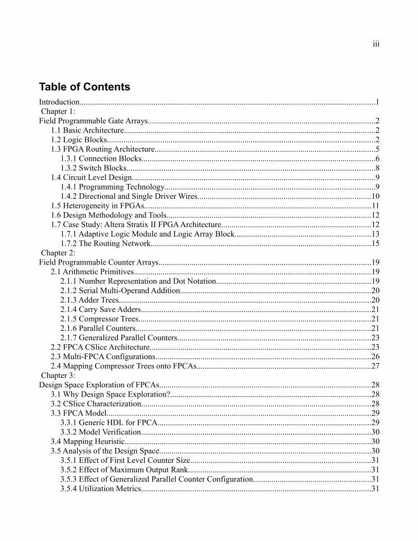
1.4.2 Directional and Single Driver WiresClassically, switch boxes and output connection boxes were implemented using pass transistors
switches (buffered/unbuffered). Using pass transistors, wires could be driven using multiple sources and signals could propagate in both directions. Recently, manufacturers have moved to directional and single driver wires [15]. In single driver wires, a wire can only be driven by a single source at one of its ends. This source is usually a multiplexer followed by a buffer driving the long wires. In this way, the extra load of several tri-state buffers is avoided and less area is wasted by unused (off) tristate buffers. Figure 1.11 shows different scenarios that could be used in routing switches.
Since the intention is to drive each wire by a single source, output connection boxes can no more be connected to channel wires using tri-state buffers. Logic block outputs can drive the wires of channels from adjacent switch boxes. Figure 1.12 shows the single driver wiring in a disjoint switch box and figure 1.13 extends this concept by merging the switch blocks and connection blocks to form a new block called a routing driver block.
Figure 1.11: Possible circuit level implementation of routing switches [19]

Chapter 1:Field Programmable Gate Arrays 11
1.5 Heterogeneity in FPGAsIn the simple island-style FPGA model which was described up to this point, all the tiles were
soft blocks of the same kind. Soft blocks are logic blocks consisting LUTs, flip-flops, etc. that can be configured to implement any logical functionality. As the technology improvement provided more on-chip area for more functionalities, it started to become more feasible to integrate hard blocks, which are
Figure 1.12: Directional and bidirectional implementation of disjoint switch box [15]
Figure 1.13: Merging switch blocks and output connection blocks into a new routing block in single driver wiring[37]

Chapter 1:Field Programmable Gate Arrays 12
essentially logic blocks with fixed functionality, beside soft blocks. The functionality provided by hard blocks could also be implemented by soft blocks, but, hard blocks are faster consume less chip area.
Memory blocks were among the first blocks which appeared on FPGAs. They were first introduced by Altera on Flex 10k devices. Xilinx Virtex II FPGA is an early of example of introduction of computational oriented blocks. This device had tiles of 18x18 multipliers in it. Newer devices like Stratix II/III devices incorporate more advanced DSP blocks. Microprocessors were also integrated into FPGAs by Altera Excalibur devices (which included an ARM core) and Xilinx Virtex II Pro devices (which included Power PC cores).
1.6 Design Methodology and ToolsThe design methodology used for finding the best architectural parameters of FPGAs is an
empirical one. A set of architectural parameters such as the number of BLEs in a CLB, switch box topology, level of connectivity in connection boxes are chosen; then the tool synthesized a set of benchmarks and maps them on architectures of interest. The user provides sufficient transistor level information to the tool to make it able to report the speed, area usage and power consumption of the implemented design on the FPGA architecture.
The justification for empirical approach instead of the analytical one is that designing an FPGA to be routable in all possible cases will need extensive resources for connectivity which is overkill for real life applications. By making decisions such as packing BLEs into a CLB with shared inputs the design parameters become dependent on certain set of (real) applications. Thus, exploration for optimal parameters using benchmark circuits is inevitable. Another approach would be to develop a raw mathematical model relating the architectural parameters of an FPGA to each other and then train the model with a set of benchmarks so that the final model captures the real demand of typical benchmarks inside it. The work done by [16] take this approach using Rent's rule and a more specific model for FPGAs is developed in [17]. It is important to note that such models are used just for analysis of routing resource demand in early stage of the design. The reliable results should be chosen after running extensive design space explorations on the benchmarks.
The Versatile Place and Route (VPR) design flow [18] is the most used tool for academic FPGA research. The HDL code for the benchmarks are first synthesized using a logic synthesis tool to a netlist of LUTs and FFs. V-Pack (or TV-Pack) is then run on the netlist to pack the LUTs and FFs with more local connections and shared inputs to a set of logic clusters (CLBs). Then, VPR places these CLBs in an FPGA – usually by means of an algorithm based on simulated annealing – and finally the routes the connections between these blocks. VPR can be run in two modes. In the first mode, no predefined channel width (number of wires in the channels) is specified; so the tool uses a binary search to find the minimum channel width by which the design in routable. The other mode fixes the channel width and determines whether or not it is possible to route the benchmarks on an architecture. Based on the published work [19],[20] it seems that the same approach is taken by industrial companies with their own internal development tools.
1.7 Case Study: Altera Stratix II FPGA ArchitectureStratix series of FPGAs is Altera's high end solutions. The architecture of the Stratix II devices
from this family is briefly introduced here. It is manufactured in a 90nm process which was available to us for comparison and was used for study of FPCA integration. The Stratix III devices which are

Chapter 1:Field Programmable Gate Arrays 13
fabricated in 65nm and recently introduced 40nm based Stratix IV devices do not show any fundamental changes compared to Stratix II devices. Figure 1.14 shows a general arrangement of building blocks of this device. Thw Stratix II is an extension of island-style FPGAs, where islands in each column are of the same kind. Apart from the block RAMs in this device, all the rest of the FPGA is composed of tiles of same height, each having a routing block, local routing and logic resources.
1.7.1 Adaptive Logic Module and Logic Array BlockThe Stratix II uses a novel basic logic element in its core which is called the Adaptive Logic
Module (ALM). An ALM contains two fracturable lookup-tables which can be configured to act as a large single LUT or two smaller ones. It also includes other advanced features such as carry-chains, arithmetic chains, and register chains. Figure 1.15 illustrates a Stratix II ALM.
Figure 1.14: General Stratix II architecture [5]

Chapter 1:Field Programmable Gate Arrays 14
Not all of the resources in the ALM are used simultaneously. The ALM can be configured to operate in different modes; in each mode only a portion of the ALM features are used. Examples of these working modes are: Normal mode, suitable for general logic applications; Extended LUT mode, in which it is possible to implement a certain set of 7 input logic functions; arithmetic mode, which makes use of carry chains; and Shared Arithmetic mode, where the shared arithmetic chain is used.
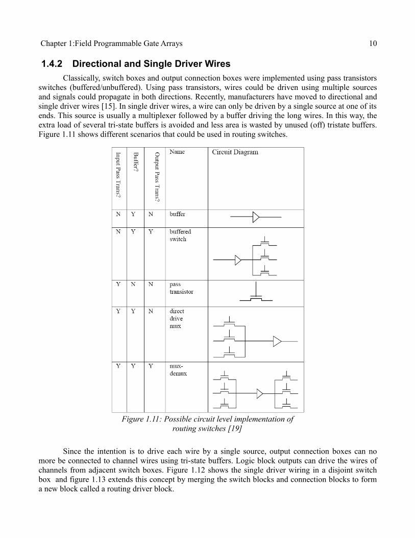
A set of 8 ALMs, a control signal generation block and local interconnections form a Logic Array Block (LAB). The numbers of ALMs in a LAB has increased in both Stratix III and Stratix IV architectures. The local interconnection is driven by the wires in horizontal and vertical channels and also by the outputs of adjacent blocks. It serves as intra-cluster interconnection multiplexers introduced before. According to [20] the intra-cluster connection is a 50% populated sparse crossbar and could be optimized analytically or using methods similar to [21]. Figure 1.16 illustrates a LAB and its main components.
Figure 1.15: Adaptive Logic Module in Stratix II device [5]
Chapter 1:Field Programmable Gate Arrays 15
1.7.2 The Routing NetworkThe MultiTrack interconnectin Stratix II devices provide the required connectivity between
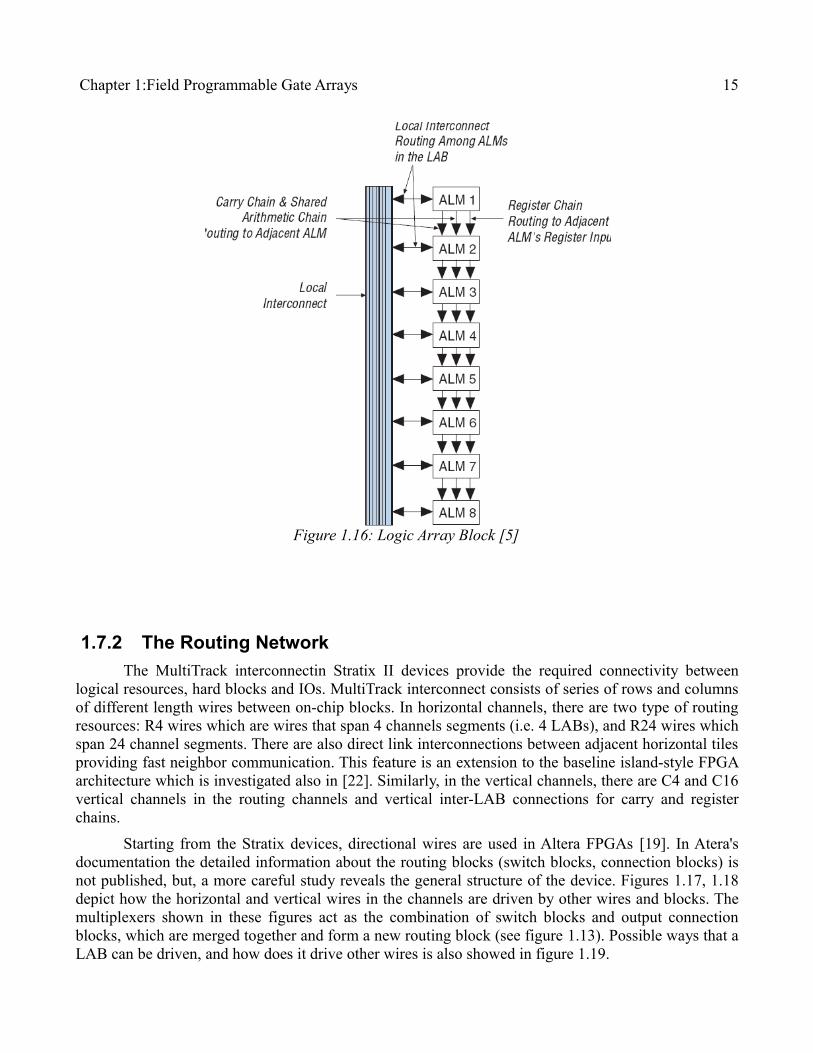
logical resources, hard blocks and IOs. MultiTrack interconnect consists of series of rows and columns of different length wires between on-chip blocks. In horizontal channels, there are two type of routing resources: R4 wires which are wires that span 4 channels segments (i.e. 4 LABs), and R24 wires which span 24 channel segments. There are also direct link interconnections between adjacent horizontal tiles providing fast neighbor communication. This feature is an extension to the baseline island-style FPGA architecture which is investigated also in [22]. Similarly, in the vertical channels, there are C4 and C16 vertical channels in the routing channels and vertical inter-LAB connections for carry and register chains.
Starting from the Stratix devices, directional wires are used in Altera FPGAs [19]. In Atera's documentation the detailed information about the routing blocks (switch blocks, connection blocks) is not published, but, a more careful study reveals the general structure of the device. Figures 1.17, 1.18 depict how the horizontal and vertical wires in the channels are driven by other wires and blocks. The multiplexers shown in these figures act as the combination of switch blocks and output connection blocks, which are merged together and form a new routing block (see figure 1.13). Possible ways that a LAB can be driven, and how does it drive other wires is also showed in figure 1.19.
Figure 1.16: Logic Array Block [5]

Chapter 1:Field Programmable Gate Arrays 16
Figure 1.17: Driving vertical lines in Stratix II routing network [5]
Chapter 1:Field Programmable Gate Arrays 17
Using the Chip Planner program – available in Quartus II package by Altera – some more details about the routing architecture of Stratix II device can be found. For example the number of wires of each fixed length in each channels is distinguishable. Table 1.1 lists this information.
Figure 1.18: Driving horizontal lines in Stratix II routing network [5]
Figure 1.19: Routing network connections to LABs [5]

Chapter 1:Field Programmable Gate Arrays 18
Table 1.1: Routing resources in Stratix II architecture
Routing Resource CountR4 Horizontal Wires 208R24 Horizontal Wires 24C4 Vertical Wires 128C16 Vertical Wires 16LAB Local Interconnect Lines 44LAB Feedback Lines 16ALM Outputs 32(16×2)

Chapter 2:Field Programmable Counter Arrays 19
Chapter 2:Field Programmable Counter Arrays
Field Programmable Counter Arrays (FPCAs) are one-dimensional array of basic computational elements called Compressor Slices (CSlices). FPCAs are configurable lattices that perform Multi- Operand Additions (MOA) efficiently. MOAs – either explicitly or implicitly in the heart of other blocks – occur frequently in arithmetic circuits used in video applications, cryptography, wireless communication, etc. In multipliers, the partial product bits generated by a level of AND gates, represent a MOA as well.
Dadda and Wallace trees [23] reduce the partial products to a two input addition. They are also referred to reduction trees. Verma and Ienne [39] have proposed a set of transformations which expose large multi-operand additions from arithmetic circuits. In this way, datapath circuits can be be implemented more effectively by specific digital circuits like FPCAs (also called here compressor trees) rather than general logic produced by using commercial synthesis tools.
This chapter starts with arithmetic primitives and then introduces the structure of FPCAs and their operation.
2.1 Arithmetic Primitives
2.1.1 Number Representation and Dot NotationIn this work, it is assumed that numbers are represented as unsigned integers. This will not
affect the generality of the problem. Negative integers, when represented in the 2's complement format, can be summed similar to unsigned numbers. Fixed point arithmetic is the same as integer arithmetic (extra rounding and saturation may be needed after the computations) and floating point units use integer and fixed point arithmetic in their core.
Let B=bn-1bn-2...b0 be an n-bit unsigned binary integer, where b0 is called the Least Significant Bit (LSB) and bn-1 is the Most Significant Bit (MSB). The subscript i is the rank of bit bi. Each bit contributes the value of bi2i to the value of B. A column is a set of bits all having the same rank. Column i is the set of bits of rank i.

Chapter 2:Field Programmable Counter Arrays 20
Figure 2.1 uses dot notation to represent a multiplication. Dot notation is used where the position and alignment (rank) of the bits is important rather than their actual values.
2.1.2 Serial Multi-Operand Addition
A sequence of two operand addition where in each stage, the next operand will be added to the accumulated sum of the previous operands can compute the result of a multi-operand addition. A serial implementation of this structure consists of an adder and an accumulation register. Figure 2.2 shows the structure of the serial solution graphically.
2.1.3 Adder TreesA faster way to implement a multi-operand addition to use an adder tree. Figure 2.3 shows the
idea of a binary adder tree where each node is a carry propagate adder. Strangely, using slow ripple carry adders may result to an overall faster design. This can be observed by careful analysis of carry propagation of adder trees [23]. An adder tree requires n-1 CPAs to implement an n-ary addition and it is a costly solution.
Figure 2.1: Dot notation representation of a 4x4 multiplication [23]
Figure 2.2: Serial addition [23]
Figure 2.3: A binary adder tree [23]
Chapter 2:Field Programmable Counter Arrays 21
Adder trees are used in FPGA based design due to the type of available resources. Adaptive Logic Modules (ALMs) in Stratix II devices and later devices in this family, can implement ternary adder trees which will result to a faster implementation compared to their counterparts [5].
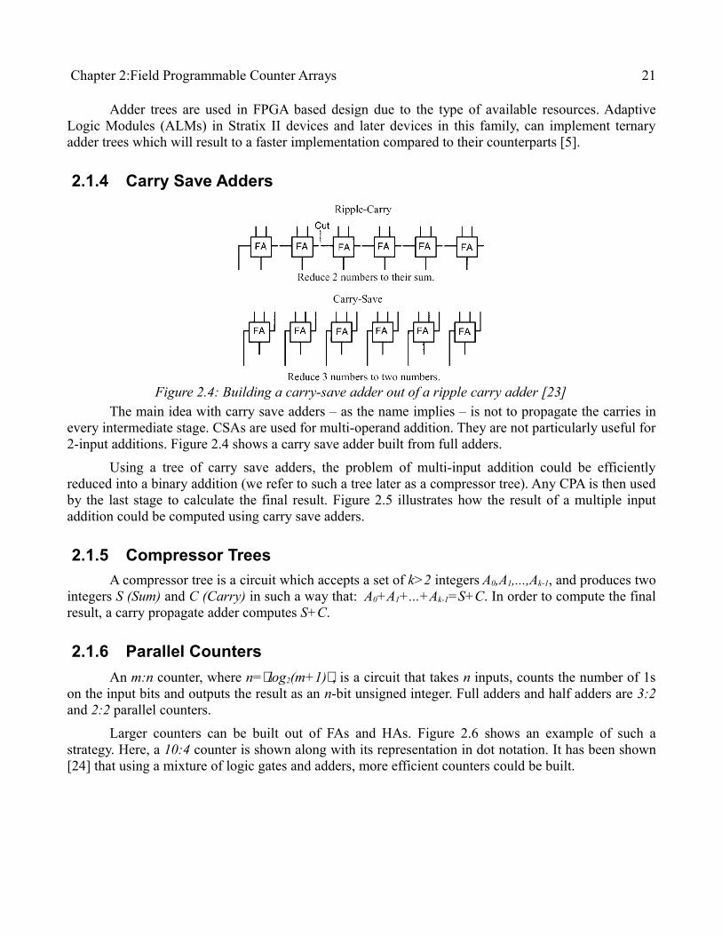
2.1.4 Carry Save Adders
The main idea with carry save adders – as the name implies – is not to propagate the carries in every intermediate stage. CSAs are used for multi-operand addition. They are not particularly useful for 2-input additions. Figure 2.4 shows a carry save adder built from full adders.
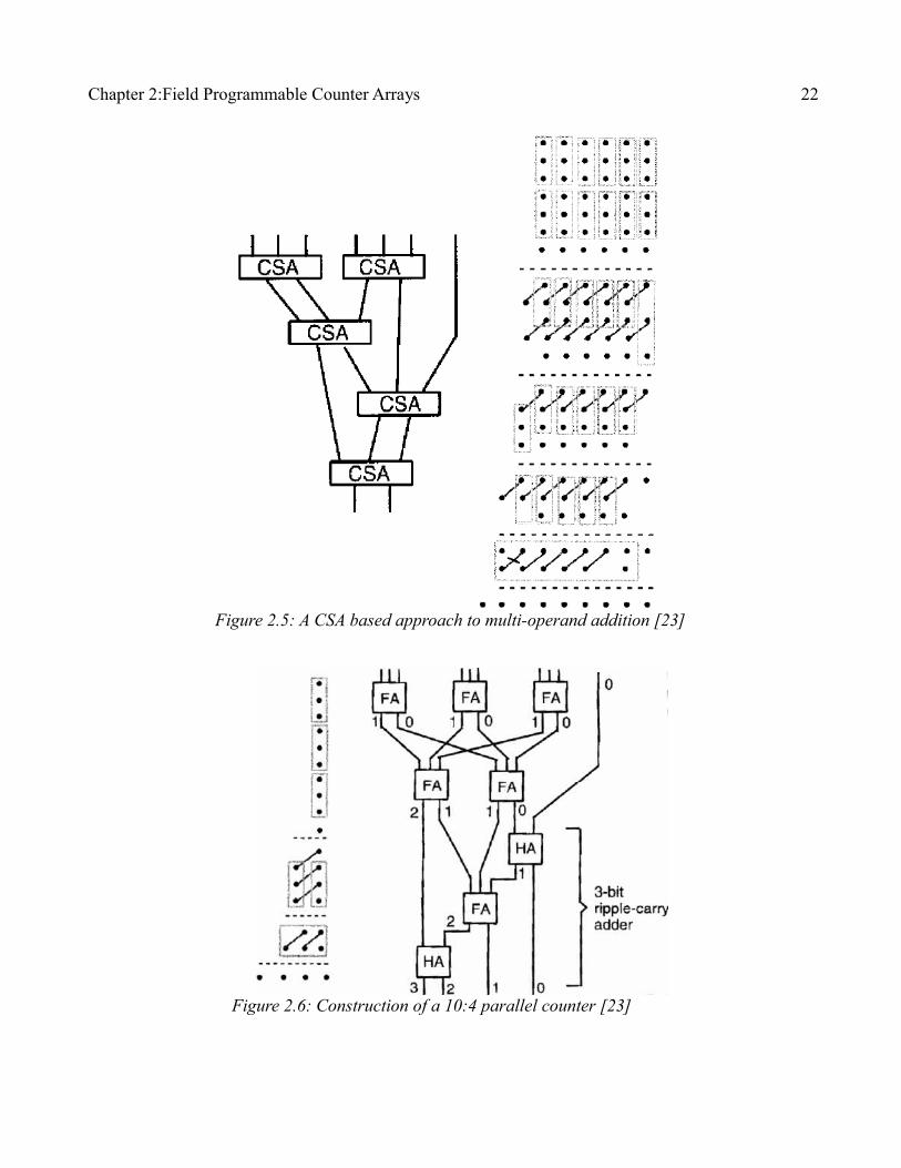
Using a tree of carry save adders, the problem of multi-input addition could be efficiently reduced into a binary addition (we refer to such a tree later as a compressor tree). Any CPA is then used by the last stage to calculate the final result. Figure 2.5 illustrates how the result of a multiple input addition could be computed using carry save adders.
2.1.5 Compressor TreesA compressor tree is a circuit which accepts a set of k>2 integers A0,A1,...,Ak-1, and produces two
integers S (Sum) and C (Carry) in such a way that: A0+A1+...+Ak-1=S+C. In order to compute the final result, a carry propagate adder computes S+C.
2.1.6 Parallel CountersAn m:n counter, where n=log2(m+1), is a circuit that takes n inputs, counts the number of 1s
on the input bits and outputs the result as an n-bit unsigned integer. Full adders and half adders are 3:2 and 2:2 parallel counters.
Larger counters can be built out of FAs and HAs. Figure 2.6 shows an example of such a strategy. Here, a 10:4 counter is shown along with its representation in dot notation. It has been shown [24] that using a mixture of logic gates and adders, more efficient counters could be built.
Figure 2.4: Building a carry-save adder out of a ripple carry adder [23]
Chapter 2:Field Programmable Counter Arrays 22
Figure 2.5: A CSA based approach to multi-operand addition [23]
Figure 2.6: Construction of a 10:4 parallel counter [23]

Chapter 2:Field Programmable Counter Arrays 23
2.1.7 Generalized Parallel CountersAn m:n parallel counter, gets its m inputs bits from the same rank i, and generates an n-bit
output of ranks i,i+1,...,i+(n-1) respectively. This can be generalized by enabling the counter to count bits of multiple ranks.
A Generalized Parallel Counter (GPC) is defined as a tuple (kn-2,kn-3,...,k0;n) where ki is the number of bits of rank i summed up by the counter and n is the number of output bits. Figure 2.7 shows examples of three GPCs. GPCs can be implemented in different ways. One way which is also used in this work, is to use an m:n counter and to connect each input bit of rank i to 2i inputs of the m:n counter.
2.2 FPCA CSlice ArchitectureAs stated previously, the goal in a carry-save based addition (or simply a compressor tree) is to
reduce an n-ary addition to a binary one. Figure 2.8 is an example in which parallel counters are employed to incrementally compress addition of 15 numbers to two numbers. First, the bits in each column i are connected to a 15:4 counter and outputs of rank i, i+1, i+2, i+3 are produced. Next, 4:3 counters are used in the same way on the resulting bit pattern. Finally, the resulting bit pattern of height 3 (i.e. addition of 3 numbers) could be reduced in the same way using 3:2 parallel counters. As can be seen, if an m:n counter is used the jth stage of the compressor tree, the counter on the j+1st stage will have a parallel counter of size n. We pack a set of counters vertically and call them a Compressor Slice (CSlice). Figure 2.9 shows an example for interconnection of CSlices.
Figure 2.7: Dot notation representation of examples of GPCs [23]

Chapter 2:Field Programmable Counter Arrays 24
The CSlice used in the FPCA is improved further in two directions. First, the first counter in the CSlice is replaced by a Configurable GPC. A Configurable GPC is a GPC which can be programmed to sum desired number of bits from each arbitrary rank. A configurable GPC is built from a parallel counter by adding two blocks to its input: A GPC Configuration Circuit (GPCCC) and an Input
Figure 2.8: Using parallel counters to reduce a compressor tree
Figure 2.9: CSlice interconnections

Chapter 2:Field Programmable Counter Arrays 25
Configuration Circuit (ICC).Consider an m:n counter. A GPCCC extends this counter to a set of GPCs (kn-2,kn-3,...,k0;n)
where the exact value of kis is configurable by the user. Figure 2.10 shows a GPCCC built for a 15:4 counter. Together with the counter, they can act as GPCs (5, 5; 4), (4, 6; 4), (3, 7; 4), (2, 8; 4), (1, 9; 4), and (0, 10; 4) by setting the appropriate configuration bits.
The user may need to use only a subset of input bits in each CSlice. The ICC lets the user limit the inputs to the CSlices by “turning off” some of the inputs to the first level GPC. This is done by driving the unused bits to '0'. An ICC can be simply built out of a layer of switches (e.g. AND gates).
The second improvement comes from the observation that the area of a CSlice is dominated mostly by the first level counter rather than rest of the counters in the compressor tree chain. This motivates replicating all the parallel counters in a CSlice (except the first level counter) and thus, make the CSlice able to produce more than one output bit. If the chain is replicate k times to produce outputs of rank 0 to k-1, the CSlice has a Maximum Output Rank Configuration (MORC) of k. The user should be able configure each CSlice to produce any number of outputs from 1 to k.
Putting All these together, an FPCA architecture can be characterized mainly by the parameters describing its CSlices. Figure 2.11 illustrates an example of a CSlice used in this work with the main parameters highlighted. The CSlice shown in this figure uses a 31:5 counter in the first level and has a MORC=2.
Figure 2.10: A GPC, built by adding a GPCCC to the input of a parallel counter

Chapter 2:Field Programmable Counter Arrays 26
2.3 Multi-FPCA ConfigurationsIt may be necessary to use more than a single FPCA to synthesize a large compressor tree. In
this case, two scenarios may happen: Horizontal configurations and Vertical configurations.
A Horizontal Configuration is needed in situations where the number of columns in the input bit pattern exceeds the number of CSlices available in a single FPCA, if more CSlices are needed to propagate the remaining carry-out bits to compute the MSBs of the result. In this case, the chain output bits of the last CSlice in the first FPCA should be connected to the chain input bits of the first CSlice in the second FPCA. Figure 2.12 shows proper interconnections needed for such a case. The chain bits could be routed between FPCAs for example through global routing resources or using fixed connections similar to HARPs [25]. HARPs replace routes which does not need so much flexibility with fixed ones to save are and improve performance.
A Vertical Configuration is needed in situations where the number of input bits (height of the input bit pattern) exceeds the input capacity of a single CSlice. If m is the capacity of a CSlice, suppose that each column has km bits. Then k CSlices (e.g. k FPCAs) are needed to compress each column; this will result in k sum bits produced per-column, one by each FPCA. Another FPCA is now required to sum the remaining bits. Figure 2.12 shows an example of such a situation with k=2. A mixture of horizontal and vertical configurations may be needed to synthesize larger compressor trees.
Figure 2.11: Example of a CSlice used in this work with MORC=1 and FCS=31:5

Chapter 2:Field Programmable Counter Arrays 27
2.4 Mapping Compressor Trees onto FPCAs
A deterministic greedy mapping heuristic is used in this work to map an input bit pattern to an FPCA. This algorithm is slightly different from the ones reported in previous work [26]. Note that the mapping heuristic is assuming single FPCA configuration. It means that the height of input bit pattern (the number of numbers being added together) is not so much so that a chain of horizontal CSlices could sum it up (No vertical FPCA configuration according to [26]). The algorithm can be easily generalized to multi-FPCA configurations. Figure 2.13 describes this algorithm in pseudo-code.
Inputs:
GPCCC architecture (mk-1,mk-2,…,m0)
Set of input columns I={ Cj | 0≤j<n}
Outputs: Number of CSlices needed
ICC configuration
GPCCC configuration
Output rank configuration
1) Start with the first CSlice and first input bit column.
2) Configure the ICC and GPCCC bits with lowest ranks to take all the bits of current column. Set output rank to 0.
3) Report fail and finish if unsuccessful.
4) If input bits of greater rank are available and we have not reached the maximum output rank:
4.1) Configure the bits with lowest remaining ranks to take as many bits of the next column as possible.
4.2) Increase the output rank if finished with next column, go to 4.
5) If more columns are available, then set the next input column to be current column and go to 2.
6) Finish.
Figure 2.13: Pseudo-code used for Mapping an input bit pattern to FPCA
Figure 2.12: Multi-FPCA configurations (a) Horizontal (b) Vertical

Chapter 3:Design Space Exploration of FPCAs 28
Chapter 3:Design Space Exploration of FPCAs
This chapter explains the methodology used for finding the optimum FPCA architectures and introduces the tools developed for this reason. The impact of the change of each parameter on performance and area is analyzed and finally, a set of configurations suitable for implementation is picked.
3.1 Why Design Space Exploration?Design Space Exploration (DSE) is a method to tackle problems where an analytical approach
is difficult to take or there is no analytical solution based on the available theories and models. FPCA architecture design – according to our investigations – falls into this group of problems. By twisting every single knob in FPCA architecture, two trends affecting the performance in opposing directions could be identified that suggest the existence of an optimum point for each parameter. Alternatively, this optimum point depends on the value of other parameters, the technology used for VLSI implementation and, most importantly, the application (benchmarks) being mapped on the FPCA.
For example, increasing the MORC of the CSlices reduces the number of CSlices required to synthesize an application on the FPCA, improves the performance by making the critical path pass through fewer output multiplexers, and saves area by using fewer first-level counters. But, if the configuration of the GPCCC or the characteristics of the benchmarks does not allow exploitation of output ranks, thicker output multiplexing layers decrease the performance, and the area dedicated to extra parallel counters columns in the CSlices are wasted.
An empirical approach could help overcoming such problems by examining all possible points in the design space, which can not be identified just by analysis.
3.2 CSlice CharacterizationDespite the complex architecture of CSlices, they are characterized by three parameters:
● The First level Counter Size (FCS)
Chapter 3:Design Space Exploration of FPCAs 29
● The Maximum Output Rank Configuration (MORC)
● The Generalized Parallel Counter Configuration Circuit (GPCCC)
Each parameter is explained in detail previously in Chapter 2.
3.3 FPCA ModelDSE is usually done on a model of the real design. This model should be sufficiently flexible to
allow the user to freely change the three parameters describing FPCAs (CSlices). Therefore, it should be generic in terms of the three aforementioned parameters.
3.3.1 Generic HDL for FPCASince the intention is to have a real hardware model on which the benchmarks could be mapped
and the area/delay values be extracted, the model is developed using synthesizable subset of VHDL. Each FPCA sub-block was modeled in a generic fashion and sub-blocks were connected together in higher level blocks (also generic). In VHDL, generic statements are used to model generic blocks. Some of these generic values are calculated using a Perl script and written to a VHDL package which is included by other modules. The rest of the model is developed in pure VHDL.
Developing a generic HDL model of FPCAs was a non-trivial task. Two of the most significant challenges were (1) Modeling parallel counters in an efficient way and (2) Modeling the interconnection of components inside a CSlice.
The first approach taken for modeling parallel counters was using behavioral VHDL as a loop in a process statement which counts the input bits and produces outputs. These models were synthesized using Synopsys Design Compiler v2006.06 and the compile_ultra optimization capability of the tool. The result for a 31:5 counter was poor. The synthesis tool could not find an efficient way to restructure the counter to produce acceptable results. One of the well known ways for efficient implementation of parallel counters is using a tree of Full-Adders and Half-Adders [23] (also described in chapter 2). In this work, based on the ability of VHDL to model recursive circuits [27] a generic adder tree is modeled to mimic a tree of full adders and half adders. The results obtained by this approach were more acceptable and comparable to manual description of fixed size counters. More advanced methods for synthesis of parallel counters are also suggested [24].
The need for correct propagation of the carry-out bits produced by the parallel counters from the current and previous CSlices, results in a complex interconnection of counters, output multiplexers, CICs and final adders. These interconnection in top-level CSlice was modeled using a combination of process statements and VHDL functions. Although the developed model is correct and was fully verified, the code itself became complex and difficult to read. One other solution was to write program in another language like Perl or C++ to generate this netlist. This will result in a clean VHDL code but the complexity is moved to another sequential language, but not reduced.
In [28] a solution called the Lava HDL was proposed. Lava HDL is built upon the functional language Haskell. Using features of a pure functional language such as lazy parameter evaluation for functions or recursive data structures, Lava has successfully modeled complex interconnections usually found in arithmetic circuits. There are two existing branches of Lava language. One was developed by Satnam Singh at Xilinx [29] and is targeted for synthesis into FPGAs, and the other is developed at Chalmers University and is intended for use in formal verification [30]. The latter was evaluated for

Chapter 3:Design Space Exploration of FPCAs 30
use in this work, but its code generation features are incomplete. Because of this, Lava was deemed insufficient for out purposes.
3.3.2 Model VerificationThe model was verified using a generic testbench developed in SystemVerilog. Instead of
verifying the model just by random stimuli generation, a more clever, white-box based approach was taken to make sure every corner in the verification space is tested.
For any given CSlice configuration, an FPCA composed of 2×FCSout-1 CSlices is formed, where FCSout is the number of output bits of the first level counter. This number of CSlices were chosen to make sure all possible bit propagations from(to) prior(next) CSlices will happen in the middle CSlice – which is the core of the design under test. In all prior CSlices, the output rank is configured to the minimum required for full bit propagation. All of the following CSlices are set to MORC so that the result would fit in the FPCA. The Input Configuration Circuit (ICC) of the first half of CSlices (including the middle one) is set to accept input bits and is disabled for the rest (propagation CSlices). Chain propagation is enabled in all CSlices, except for the first one.
The simulation runs as follows: First in an outer loop, a random rank configuration for the CSlices is produced. The FPCA is then programmed in a configuration stage using these values together with the desired configuration of output multiplexers, CICs, and ICCs. Then in an inner loop, several input bit patterns are generated and fed to the FPCA. The summation of the input bit pattern is calculated by the testbench and compared against the output of the FPCA. An error is generated in case of presence of any mismatch.
This testbench could be improved further by using methods such as coverage based analysis. This is left open for future work.
3.4 Mapping HeuristicThe mapping heuristic is written in Perl and embedded in a module called mapping. The output
of the program is a TCL script used by the synthesis tool. This script is a sequence of set_case_analysis [31] commands which is used to set constants on the output ports of the configuration bits. In this way, the tool is instructed to remove all the false paths (without optimizing them away) so that the timing analyzer could report the delay for the real critical path of the design. If this step in neglected, the critical path of the FPCA – viewed as a logic circuit – exceeds the critical path of the compressor tree synthesized on it.
3.5 Analysis of the Design SpaceBefore searching every single point in the design space for the best architectures blindly, it is
useful to analyze the expected trends and reduce the size of the search space by identifying the sub-optimal architectures. Also we intend to have a tool by which we can observe the utolization of the logic resources of the FPCAs. It is useful to restrict the design space further by exploring only the most promising architectures. This is why Utilization Metrics are introduced to be used in design space exploration.

Chapter 3:Design Space Exploration of FPCAs 31
3.5.1 Effect of First Level Counter SizeIncreasing the size of the FCS increases the input bandwidth of the FPCA/CSlice. The FCS is
the largest component in a CSlice, so increasing its size entails a significant area overhead per CSlice. The Compression Ratio of an m:n counter is the ratio m/n of the number of input to output bits: for a fixed number of output bits n, m/n is maximal when m = 2n – 1. As the goal of an FPCA is to compress a large number of input bits down to 2-per-column, counters with higher compression ratios are the most effective. Our DSE considered 15:4 and 31:5 counters, which are maximal for 4 and 5 output bits respectively. For the benchmarks considered in this work, 63:6 counters are simply too large, and lead to both excessive delay and area.
3.5.2 Effect of Maximum Output RankIn these experiments, MORCs of size 0, 1, and 2 is considered; based on the analysis in section
3.1 and the results coming out of conducting a few random experiments, it was observed that increasing the MORC of the CSlice beyond 1 degrades both delay and area significantly, so larger MORCs were not explored. As stated before, the reduction in area is due to the fact that an increased MORC allows one CSlice (whose area is dominated by the FCS) to produce multiple output bits, thereby requiring fewer CSlices; the increase in delay is due to the unavoidable introduction of chain output multiplexers , especially into the CPA path, for MORCs larger than 0.
3.5.3 Effect of Generalized Parallel Counter ConfigurationThe GPC configuration circuit allows a CSlice to grab bits of higher ranks for summation. It
can not be easily determined what would the best architecture for the GPCCC. More inputs bits of larger maximum rank in GPCCC will lead to having fewer bits coming into each CSlice and will increase the probability of failing to map input bit patterns; however, the input interconnection routing would be less complex and the CSlice could theoretically finish bits in more columns of input bit patterns (which will translate to production of more output bits per CSlice). To the contrary, assigning a lower maximum rank to GPCCC inputs will enable the CSlice to take more input bits and map a larger set of input bit patterns, but it will increase the input routing demand and also possibly under-utilize the CSlice for the input bit patterns with lower height.
3.5.4 Utilization MetricsPerforming the DSE on larger circuits and benchmarks increases the runtime significantly. Also,
the final area/delay values resulting from mapping a compressor tree onto an FPCA, does not provide a direct or intuitive insight on the utilization of the available resources. The goal is to introduce a metric by which the designer can prune the design space to an acceptable size and then perform the DSE on the remaining competing architectures.
On a family of CSlice architectures with fixed MORC and FCS, where just the GPCCC is varied, the number of CSlices on which the benchmarks are mapped is a good measure of performance and area usage. This value can be determined by the mapping heuristic alone without the need for synthesis. But it is not particullary useful when applied for comparison between other architectures. This is because two benchmarks may map onto the same number of CSlices, but using different architectures with difference area and delay metrics. Therefore, there is a need to introduce a metric that (1) is fast to calculate and does not need the long hardware synthesis for each structure; and (2) is
Chapter 3:Design Space Exploration of FPCAs 32
general enough to permit comparison between all architectures.
The input utilization of a CSlice measures its ability to consume bits, i.e., in general, the more bits consumed, per CSlice, then the fewer CSlices are required for the benchmark. The most obvious measurement of input utilization is the number of input bits mapped to each CSlice; however, this is skewed by the GPCCC. For example, let FCS = 15:4; a GPCCC of (0, 15; 4) allows up to 15 inputs; on the other hand, a GPCCC of (5, 5; 4) has up to 10 inputs, but greater flexibility in mapping. Comparing the input utilization of the two is difficult, since in the end, all input bits of the FCS will be used. Suppose that N CSlices are used, and the FCS is an m:n counter; now, let X be the total number of input bits to the first counter that are not driven to 0 by the GPCCC after mapping. Then the input utilization is defined to be the quantity Uin = X/(Nm). For example, if a CSlice is configured as a (5, 5; 4) GPC and two bits of rank 1 and four bits of rank 0 are mapped onto the CSlice, then Uin = (2×21 + 4×20)/15 = 8/15 = 0.53.
The output utilization, Uout, is defined for CSlices whose MORC exceed 0. Recall, for a given MORC k-1, the ORC can be configured to any value j, 0 < j < k-1, i.e. the CSlice can produce 1 to k output bits (j+1 output bits); let Oi be 1 plus the ORC of the ith CSlice in the FPCA. Then:
U out=∑i=1
N
O i
k N −1
We define Utilization as U=Uin×Uout. This value is more usable and meaningful if there exists a correlation between input and output utilizations.
Note that in this work, the utilization metrics are not used to prune the design space. The exploration is done fully and the utilization metrics are also computed in parallel. The goal is to prove the usefulness of these metrics for future larger explorations.
3.6 Experimental Results
3.6.1 Tools and MethodologyBased on the generic FPCA model, a set of benchmarks are mapped onto different FPCA
architectures using the mapping heuristic and the area/delay results are then reported.
A module named fpca_gen accepts the three parameters that describes the FPCA architecture and generates a set of VHDL files that implement the circuit, a script file for proper synthesis of the architecture, and a testbench for verification implemented in SystemVerilog. A top-level module called explore generates (the parameters of) all possible CSlice architectures; explore calls fpca_gen to generate each architecture; for each benchmark, explore calls mapping to synthesize the benchmark and consequently, invokes the synthesis tool to estimates area and delay. Figure 3.1 illustrates this operation.

Chapter 3:Design Space Exploration of FPCAs 33
The two FCSs and three MORCs (based on analysis in section 3.5) result to six CSlice architecture descriptions, for which only the GPCCC is varied (the ICC is inferred from the GPCCC). Doing complete synthesis of the architecture in every single case increases the exploration time and also introduces a high level of non-determinism resulted by the synthesis tool. To cope with this, the non-GPCCC/ICC portions of the baseline CSlices were synthesized and optimized separately and saved in a library. During the DSE, only the GPCCCs/ICCs are generated anew and synthesized; the rest of the CSlice is invoked from the library.
The synthesis tool is Synopsys Design Compiler v2006.06 and the technology process used for implementation is TSMC 90nm with an Artisan standard cell library.
3.6.2 BenchmarksA set of 7 arithmetic benchmarks were selected to be used in the DSE; our goal was to find a
mixture of benchmarks with a variety of bit patterns (i.e., rectangular for multi-input addition, trapezoidal for multiplication, irregular for filters). The same experiments could be repeated with a larger set of benchmarks and fewer restrictions on the FPCA configurations.
The benchmarks are listed in Table 3.1; they include the compressor trees for three different multipliers, two multi-input addition operations, a FIR filter [26], and the Sum-of-Absolute-Difference (SAD) computation, which is used for motion estimation in video coding algorithms, such as H.264/AVC. mul5x5, was selected based on an anecdote in a paper by Kuon and Rose [1]: mul5x5 performs better on the general logic of an FPGA than the dedicated 9x9 multiplier in the embedded DSP blocks. mul36x18 could represent either a standard 36x18 multiplier, or a 36x36 multiplier with Booth encoding. mul18x18, mul36x18, add16x16, and FIR were too large to fit on an FPCA whose CSlices have an FCS of 15:4; the remaining benchmarks fit on FPCAs whose CSlices have both 15:4 and 31:5 FCSs.
Figure 3.1: Functional operation of the DSE tool
explore
FCS, MORC,Input Bit Pattern
Total Area/Delayfor FPCAs with each GPCCC
fpca_gen mapping synthesis

Chapter 3:Design Space Exploration of FPCAs 34
Table 3.1: Benchmark circuits used for DSE
Benchmark Description FPCAs(FCS) Mapped
mul5x5 5x5 Multiplication 15:4, 31:5
mul18x18 18x18 Multiplication 31:5
mul36x18 36x18 Multiplication 31:5
add8x32 Add 8 32-bit Integers 15:4, 31:5
add16x16 Add 16 16-bit Integers 31:5
FIR FIR Filter 31:5
SAD Sum-of-Absolute-Differences 15:4, 31:5
3.6.3 ResultsFigures 3.2-3.6 are the results of the DSE on the benchmarks.
● Each column of three sub-figures relates to a single run of the tool with a fixed MORC and FCS, while varying GPCCC.
● The top figure in each column plots the utilization metric for each GPCCC architecture. A few of the best performing architectures (in terms of utilization) are highlighted. Notice that the order of points in the x-axis is just related to the order in which the tool generates different architectures. Each increase and decrease in the utilization values is caused by a sweep in GPCCC architecture. For example the first sweep starts with a GPCCC of (31;5) continues with (1,29;5), (2,27;5), ... and ends with (15,1;5). Next sweep starts with (1,0,27) then continues with (1,1,25) and so on. The reason that some MORCs has fewer GPCCCs is that fewer architectures were able to map the corresponding benchmark.
● In the middle figures, each architecture is plotted in the area-delay space using a single dot. As can be seen, architectures of the same rank show a linear corellation between delay and area. This is mainly because the area and delay values are both strongly correlated to the number of CSlices required for each benchmark. The small deviations in area values are due to changes in size of the GPCCCs (and consequently, ICCs).
● The bottom figures, replicate the proceeding once, but, only plot the architectures with best utilization. The result is clear: The best architectures in terms of area and delay are among the ones with highest utilization values. This supports the use of utilization to prune the search space before running the DSE.
● One other point worth mentioning is the performance of architectures with MORC=0. In these architectures, the utilization is constant everywhere and each benchmark always maps to the same number of CSlices. The reason is that the limiting factor is always the number of output bits produced by each CSlice. As a result, the delay values for the GPCCC architectures remains the same but there is a small difference in their area values due to the change in GPCCC and ICC.

Chapter 3:Design Space Exploration of FPCAs 35
Figure 3.2: DSE results for mul5x5 benchmark with FCS=15,31

Chapter 3:Design Space Exploration of FPCAs 36
Figure 3.3: DSE results for mul18x18 and add16x16 benchmarks with FCS=31

Chapter 3:Design Space Exploration of FPCAs 37
Figure 3.4: DSE results for add8x32 benchmark with FCS=15,31

Chapter 3:Design Space Exploration of FPCAs 38
Figure 3.5: DSE results for SAD benchmark with FCS=15,31

Chapter 3:Design Space Exploration of FPCAs 39
Figure 3.6: DSE results for mul36x18 and FIR benchmarks with FCS=31

Chapter 3:Design Space Exploration of FPCAs 40
To compare the different FPCA architectures against one another, for each FCS, the average area and delay values for each benchmark with different MORCs are put together and sorted. Only the GPCCC architectures which were able to map all benchmarks were chosen for this experiment. The results are presented in figure 3.7. The two figures in the first column are for FCS=15 and the ones in second column are for FCS=31. The first row represents delay values and the second row is dedicated to area values for each GPCCCC. Since all of the CSlice architectures with MORC=0 and FCS=31 have almost the same performance, only one representative is chosen among them. For FCS=31, since many GPCCC architectures were able to map all the benchmarks, only the best and worst performing architectures were chosen for comparison. For area comparison of FCS=31, one representative architecture with MORC=0 was inserted in final results manually for comparison; although it was not among the best or worst performing architectures.
Figure 3.7: Average area/delay results on different GPCCC architectures for FCS=15,31.

Chapter 3:Design Space Exploration of FPCAs 41
Initially it may seem that FPCA architectures with FCS=15 perform better than the ones with FCS=31; however this is not true since they only map the smallest subset of benchmarks.
We chose to pick the best FPCA from the ones with FCS=31 since we want to be able to map all of the benchmarks of typical size. Note that it is also possible to map larger circuits on architectures with smaller FCS using vertical configurations, but, this involves extra area and delay of the routing architecture.
There are 6 architectures which appear both in the best area and best delay candidates: (11,9;5), (10,11;5), (12,7;5), (13,5;5), (1,9,9;5) and (1,10,7;5), all of them with MORC=1. Their performance is almost the same. We chose (13,5;5) for the rest of work because it has the lowest number of inputs (13+5=18) and thus demands less routing architecture complexity compared to other architectures. If the I/O restriction of FPCAs is a more severe issue, restrictions can be defined for the DSE tool to generate and compare only CSlices with a pre-determined number of I/Os.
Recall from section 3.5.4 the definition of utilization metrics. It was assumed that there is a correlation between the input and output utilizations; so that they could be easily combined to a single meaningful metric. To investigate this issue, input and output utilizations for two benchmarks are presented in figure 3.8. As it is apparent, Uin and Uout closely follow the same trend.
Figure 3.8: The correlation between Uin and Uout values.

Chapter 3:Design Space Exploration of FPCAs 42
One other assumption that was made during the DSE is that limiting the MORC to 0, 1 and 2 and that limiting the FCS to 15 and 31 are both reasonable. The intuitive justification which was supported by limited exploration in design space, was that moving to higher MORCs and FPCs increases the area and delay without improving utilization. This was verified using the utilization metric without performing hardware synthesis and timing analysis during DSE. The best average utilization values on all benchmarks were chosen for each MORC and FCS. The investigation was extended to FPCA architectures with MORC=3 in FCS=63:6. The result is illustrated in figure 3.9. A single local maximum (which is the global maximum) is expected for the trends resulted by fixing MORC or FCS. This pick value seems to be the point with MORC=1 and FCS=31:5. The nearest point is MORC=2 and FCS=63:6 which achieves similar utilization, but with a more complicated implementation due to larger counters.
Figure 3.9: Best average utilization values for different architectures.

Chapter 4:FPCA Integration with FPGAs 43
Chapter 4:FPCA Integration with FPGAs
This chapter presents an study of the issues related to integration of hard blocks (and/or coarse-grained blocks) into FPGAs. It then proposes some integration scenarios for FPCAs and describes a generic platform for implementation and evaluation of some of these scenarios based on Stratix II devices and the FPCA architecture chosen in chapter 3.
4.1 The ProblemThe introduction of hard logic blocks and coarse-grained blocks for FPGAs create a new
problem: their seamless integration. In simple words, the problem asks how should these blocks be floorplanned and placed in the homogeneous array of soft logic, and how should they be connected to the routing fabric efficiently? The floorplan should result in shorter critical paths and reduced congestion and an interface must be designed for the block that meets the following requirements:
● It should provide the required level of connectivity (i.e. all typical circuits using the block should be routable).
● It should be fast and consume minimum chip area.
● It should minimize the negative impact on the routability of other blocks.
4.2 Related WorksAlthough there has been significant study on new architectures for hard and coarse-grained
blocks for FPGAs, few of them have studied their detailed interface. In [32], formal optimization methods are used to design mixed-granularity FPGA architectures. Integer Linear Programming(ILP) is incorporated to determine the best floor plan to optimize the architecture for a set of DSP applications, including the choice of the best mix of hard 18×18-bit multipliers.
A similar problem is studied for block RAMs in [33]. In this work, without any investigation and inspired by commercial FPGAs, it is assumed that a row of block RAMs is located in the middle of the chip (like figure 4.1). The authors have tried to determine the ideal flexibility of the memory/logic

Chapter 4:FPCA Integration with FPGAs 44
interconnect block (illustrated in figure 4.2). Like the connection blocks studied in chapter 1, the flexibility of a memory/logic block is defined as the number of (or portion of) available routing wires to which each memory pin is connected. This study shows that if the flexibility is too low, many circuits become unroutable, while excessive large flexibility values increase the memory access time and also waste chip area. Alternatively, the authors have made several enhancements to the routing architecture based on the characteristics of memory-to-memory connections, such as busses, in their benchmark circuits. Since nets connecting to multiple memory blocks are common in many circuits blocks, the authors have proposed to add additional programmable switches between adjacent memories to support these nets. This significantly improved the results on architectures with lower interconnect block flexibility.
The large M-RAM blocks in Stratix II device (figure 1.14) resemble this style of integration. This solution enhances the ability to tile an island-style architecture, and requires a completely new design for interfacing with the rest of routing fabric. Greater integrity and speed are achieved with larger hardwired blocks, but the layout design and interface design becomes a more complicated.
It doesn't seem that the results obtained for memory block integration could be used for arithmetic blocks such as FPCAs. The functionality of the pins and their contribution to total routing resource demand are different for blocks with different functionalities.
Figure 4.1: An example of integrating RAMs as hard blocks [32]

Chapter 4:FPCA Integration with FPGAs 45
A very recent work ([34]), has studied the integration of coarse grained Floating Point Units (FPUs) in a fine-grained soft logic array. Different floorplanning strategies for placement of the FPUs, different aspect ratios and possible pin placement methods are evaluated to find the optimum architecture. The approach taken is again an empirical one based on the delay and minimum channel width requirement of a set of benchmarks. Unlike the previous approach, they have assumed that the gridded routing fabric extends over their Embedded Blocks (EBs). Figure 4.3 shows a scenario where a 3×3 super-tile is replaced by an embedded block.
Figure 4.2: Example of memory/logic interconnect block [32]
Figure 4.3: Expansion of the gridded routing fabric over the embedded block [33]

Chapter 4:FPCA Integration with FPGAs 46
The M512 RAMs, M4K RAMs, and the DSP blocks in Stratix II devices are examples of this approach, but with a small difference. Tiles in the same column are all of the same kind. These tiles are all the same height (or multiples of same height) but their widths may slightly differ. In this way, the general routing fabric could be designed as easily as the general island-style routing fabric consisting of horizontal and vertical channels of routing wires with switch blocks in their intersections points. The problem of interconnect interface block design in this approach, will be to minimize the re-design of the intra-cluster connections in such a way that matches the actual pin-demand of the new hard blocks.
As an example, the DSP blocks in the Stratix II architecture span 4 blocks vertically. The blocks are designed in such a way that they can be decomposed into four tiles. Each tile has the same height as other logic tiles and has a switch box, intra-cluster connections and the DSP core itself. The intra-cluster connection design for DSP blocks is interesting. LAB tiles in Stratix II devices have 45 local interconnect lines that are selected by a level of switches from the general routing network. These lines drive all the ALM inputs which are around 65 input pins.For the DSP tiles (¼ each DSP block), there are 60 local lines that drive approximately 40 input pins. This information is summarized in table 4.1. The reason for this local interconnect-input pin difference is that it is the actual pin-demand of the tiles which is important, not just the number of input pins. Many of the 65 input pins of the ALMs in each LAB could be shared or driven by the local feedback lines. This lowers the actual pin demand to 44. On the other hand, DSP block input pins are arithmetic bits, which are all distinct, and needed to be routed separately. Thus, more connections than the total number of input pins are provided by the local lines to ensure the required routing flexibility. FPCAs, from this point of view, are more similar to DSP blocks than to block RAMs.
Tile Type Local Interconnect Lines Input PinsLAB Tile 44 ≅65DSP Tile 60 ≅40
Table 4.1: Intra-cluster design of LAB and DSP tilesHard blocks improve the area and speed of the designs mapped to FPGAs, but only if they are
used. Otherwise, the silicon area devoted to them and, the expensive routing resources around them are wasted. This also suggests that the integration of hard blocks is only feasible if they are used often. Shadow clusters are introduced in [35],[36] to take better advantage of the routing resources around hard blocks, when they are not used. A shadow cluster, is a soft logic block, placed “behind” the hard block so that if the design doesn't use the hard block, then some general FPGA logic within the shadow cluster can be used to implement a portion of the real circuit. Shadow clusters come at the expense of additional area, but, if properly used, the advantage obtained by making better usage of the routing network dominates this extra area overhead. Figure 4.4 depicts this idea. The inputs, which come from the routing network, are shared between the shadow cluster and the hard block. Depending on the mode of operation, either the output of hard block or the shadow cluster is selected.

Chapter 4:FPCA Integration with FPGAs 47
4.3 FPCA Integration ScenariosFPCAs, can also be viewed as programmable, but hard blocks which should be integrated into a
homogeneous array of soft blocks. The main differentiation property of these blocks that distinguishes them from embedded memories and DSP blocks is their high pin-demand relative to their silicon area. Here, some possible integration schemes based on the previous work in this area, along with the properties of FPCAs are discussed, together with their advantages and disadvantages. The baseline FPGA architecture used for this investigation is a Stratix II device.
4.3.1 Area Based IntegrationThe simplest approach is to estimate how many CSlices would have an equivalent area to 8
ALMs in an Altera Stratix II LAB. Then, we design an FPCA with this number of CSlices together with its local interconnection network and replace some of the LABs (for example two column of LABs) in a Stratix II device with the new block.
A set of 8 ALMs and an 8-CSlice FPCA were synthesized based on the descriptions in section 4.4. The final area results of them were comparable. The FPCA required 15% less area than 8 ALMs. An 8-CSlice FPCA would require 8×18=144 bits to be routed to its inputs; while a LAB interface – as is - could only provide a maximum of 44 different nets (the number of local LAB lines). The chain input bits are not counted in this calculation and are assumed to be routed through special network (e.g. HArd-wired Routing Pattern, or HARP, like networks[25]); taking them into account would make the situation even worse. This is a considerable mismatch and probably would lead to widespread in routability failures for most non-trivial benchmarks. One possible solution is to increase the routing resources in the device (e.g. number of wires in the channels and local lines). The problem with this workaround is that if the tile-based island-style FPGA architecture is to be preserved, the channel width should be increased uniformly across the whole device, resulting in a waste of area in regions where these extra routing resources are not needed. Figure 4.5 illustrates this approach.
Figure 4.4: Illustration of shadow cluster concept [34]

Chapter 4:FPCA Integration with FPGAs 48
4.3.2 Pin-Demand Based IntegrationThe configurable routing network consumes the majority of on-chip area. Thus, our intention is
not to increase the routing resources. To solve the pin-demand mismatch problem, at least four of the LABs are replaced with a single FPCA. Figure 4.6 presents this idea in a more declarative fashion. This approach was taken in previous work [26], but they have estimated the number of tiles to be 6, using a different, yet unspecified, approach. They have also taken into account the chain input and outputs of the FPCAs.
Another way to solve the problem using similar reasoning would be to decrease the number of CSlices in the FPCA so that their pin-demand matches that of ordinary LABs. 2 CSlices per FPCA tile would meet the pin demand.
Figure 4.5: Area-based integration of FPCAs
LAB
b b’ b’ b’ b’
b’ b’ b’ b’
FPCA
kb
LAB
b
LAB
b
LAB
b
LAB
b
FPCA
kb
LAB
b
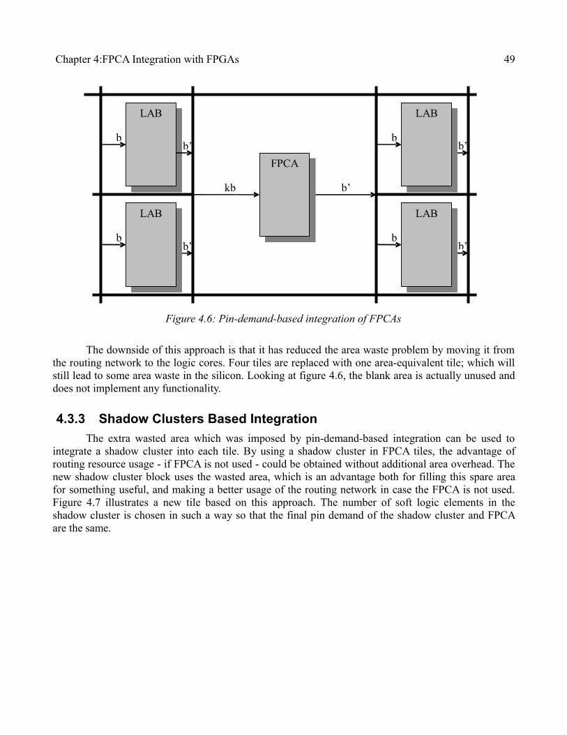
Chapter 4:FPCA Integration with FPGAs 49
The downside of this approach is that it has reduced the area waste problem by moving it from the routing network to the logic cores. Four tiles are replaced with one area-equivalent tile; which will still lead to some area waste in the silicon. Looking at figure 4.6, the blank area is actually unused and does not implement any functionality.
4.3.3 Shadow Clusters Based IntegrationThe extra wasted area which was imposed by pin-demand-based integration can be used to
integrate a shadow cluster into each tile. By using a shadow cluster in FPCA tiles, the advantage of routing resource usage - if FPCA is not used - could be obtained without additional area overhead. The new shadow cluster block uses the wasted area, which is an advantage both for filling this spare area for something useful, and making a better usage of the routing network in case the FPCA is not used. Figure 4.7 illustrates a new tile based on this approach. The number of soft logic elements in the shadow cluster is chosen in such a way so that the final pin demand of the shadow cluster and FPCA are the same.
Figure 4.6: Pin-demand-based integration of FPCAs
LAB
b b’
b’
b’
b’ b’
FPCA
LAB
b
LAB
b
LAB
b
kb

Chapter 4:FPCA Integration with FPGAs 50
4.3.4 Shadow Cluster - Extra Usage-Based IntegrationThe shadow cluster, which resides in an FPCA tile, may be used to generate the inputs of the
FPCA beside it. In this way, both the FPCA and shadow cluster could be used together, making full usage of chip area in the tile. Apart from this, local connections from LABs to the FPCA are faster compared to the ones routed through general routing network. Figure 4.8 shows the connections needed for such an operation.
An example of application that can be implemented in shadow clusters is partial product generation, the first layer of logic in a parallel multiplier. Consider the case where there are three LABs acting as the shadow cluster for an 8-CSlice tile (this would result in good area usage and a pin demand match based on the calculations in section 4.2.4), and connected in a way similar to the one shown in figure 4.8. If the goal is to implement a 6×8-bit parallel multiplier, one way based on the approach in section 4.3.2 is to calculate the 48 partial product bits in other tiles of the FPGA and route them to the FPCA tile. Alternatively, these 48 partial product bits can be generated by the shadow cluster and routed directly from their 3×16 =48 outputs to the FPCA inputs. The 8-CSlices in the FPCA is sufficient to reduce this input bit pattern and generate the result. In this way, only 6+8=14 nets should be routed to the tile (instead of 48) and no extra soft logic resources are needed.
Figure 4.7: Shadow cluster based integration of FPCAs
Routing Network
LAB
FPCA
Routing Network
LAB

Chapter 4:FPCA Integration with FPGAs 51
It may be desirable to modify the soft logic in the shadow cluster to make it more compact and optimize it for operations that generate the input bit patterns suitable for FPCAs. This is left open for future work.
One important issue that is not mentioned in shadow cluster-based and shadow cluster - extra usage-based integration is configuration memory sharing. VLSI implementations (to be discussed shortly) show that almost half of the tile area (and ALM and CSlice area) is devoted to configuration bits. In shadow cluster-based integration, where either the FPCA or the shadow cluster, but not both, operate at the same time, these bits could be shared. This resource sharing can not happen in the shadow cluster – extra usage mode.
4.4 Modeling and ImplementationTo provide a proof of concept, the integration scenarios presented in the previous section were
modeled in VHDL, synthesized, placed and routed as semi-custom designs. The FPCA model developed in chapter 3 was modified as well: configuration flip-flops were replaced with latches. In this way, more area will be saved and implementation becomes closer to real configurable devices where SRAMs are used to store the configurations. Also, Altera ALM models which were developed in previous work was modified to use latches. Synopsys Design Compiler 2007.12-SP3 using the UMC 90nm process in conjunction with Faraday standard cell libraries were used for synthesis. The tool used for place and route is Cadence SoC Encounter 5.2. The tools that generate the baseline FPGA and each of the integration scenarios are parameterized so that they could be used for exploration reasons and future studies. Appendix B provides more information about this architecture.
The baseline FPGA architecture is a simplified version of the Stratix II device that was also used in previous analyses. A switch block and the connections block that drives the logic inputs reside in a tile along with a LAB. The detailed routing architecture uses directional wiring as described in section 1.7. Figure 4.9 illustrates one tile of the baseline FPGA. This figure is comparable to figure 1.19, in Altera's documentation.
The modified disjoint block for single driver wires [15] (see figure 1.12) is used for a switch block. This model supports multi-segment wires, which span multiple switches before termination. The switch block also serves as the output connection block , making it similar to the routing driver block,
Figure 4.8: Shadow cluster - extra usage based integration.
Routing Network
LAB
FPCA
Routing Network
LAB

Chapter 4:FPCA Integration with FPGAs 52
and routes the wires from the outputs of the LAB in the same tile and the LAB in the tile residing to its right. The modeled switch is tunable for different channel widths and different wire-lengths and arbitrary bitwidths from LAB outputs; however, it does not support more than one wire length in the channels simultaneously, and it assumes there are same number of wires in both vertical and horizontal channels.
The Input Interconnection Block (IIB) is based on the model presented in [8] (figures 1.6, 1.7). The model can be configured for different number of inputs per ALM, denoted by k; number of ALMs in LAB, denoted by N; total number of inputs from the routing network, denoted by M; and a flexibility trade-off value, denoted by p (figure 1.8).
In the place and route stage, the switch was floorplanned manually and first, the wires in channels were routed to ensure straight layout of routing channels. The rest of the design were placed and routed automatically.
Figure 4.10 is the proof of concept layout of the baseline FPGA tile. It is floor planned with an aspect ratio of 1:2 (H:V) as like the real Stratix II device tiles. Figure 4.11 shows how pins of adjacent tiles align together so that the tiles could be easily replicated. The area consumed by the tile is 51842μm2.
The integration scenarios described in section 4.3 were synthesized, placed and routed to ensure the validity of the ideas. More efficient VSLI design and report of results were left for future studies.
Figure 4.9: Block diagram of the baseline FPGA tile used for implementation
VChannelLABIIB
VChannel
SwitchBlock
H ChannelSwitchBlock
SwitchBlock
H ChannelSwitchBlock
Basic FPGA Tile
Direct interconnects to adjacent tile

Chapter 4:FPCA Integration with FPGAs 53
Figure 4.10: Proof of concept layout of baseline FPGA tile
Figure 4.11: Alignment of pins for tile-ability of the design.

Chapter 4:FPCA Integration with FPGAs 54
Summary and ConclusionsA design space exploration tool for FPCAs consisting of a generic model of FPCAs, a mapping
heuristic with synthesis and report automation facilities were developed. An analysis of the design space was perfomed and a new metric called utilization were suggested to prune the DSE. A set of benchmarks were chosen and the DSE were performed, and some of the best performing architectures in terms of speed and area were highlighted.
The problem of integrating FPCAs with FPGAs was also studied. Considerations and problems were described and a set of possible integration schemes were introduced. To provide the applicability, a VLSI implementation of them was created a semi-custom design.
Future WorkThe design space exploration can be repeated:
● On more representative benchmarks
● On other architectures (e.g. using faster CPAs)
● With other mapping heuristics
● On a faster model of the FPCA
● With taking into account routing delays
A synthesis, place & route CAD flow for the hybrid device could also be developed. Since the baseline FPGA architecture chosen in this work is an Altera Stratix II device, the Quartus II software could be used to synthesize and place the benchmarks. A routing tool (like VPR) could then be developed for final routing and configuration bitstream generation for the final device.
Further, a design space exploration to find more efficient hybrid FPGA/FPCA architectures can be performed. In this way, the cost of each integration scenario could be investigated more quantitatively.
Better and more accurate VSLI implementation (e.g. custom layout design) will result in smaller and faster circuits especially for the routing architecture. This could make the results directly comparable to commercially available FPGAs.

Chapter 4:FPCA Integration with FPGAs 55
References[1] I. Kuon and J. Rose, “Measuring the Gap Between FPGAs and ASICs,” Computer-Aided Design
of Integrated Circuits and Systems, IEEE Transactions on, vol. 26, 2007, pp. 203-215.
[2] P. Brisk et al., “Enhancing FPGA Performance for Arithmetic Circuits,” Design Automation Conference, 2007. DAC '07. 44th ACM/IEEE, 2007, pp. 334-337.
[3] E. Ahmed and J. Rose, “The effect of LUT and cluster size on deep-submicron FPGA performance and density,” Very Large Scale Integration (VLSI) Systems, IEEE Transactions on, vol. 12, 2004, pp. 288-298.
[4] A. Ye and J. Rose, “Using bus-based connections to improve field-programmable gate-array density for implementing datapath circuits,” Very Large Scale Integration (VLSI) Systems, IEEE Transactions on, vol. 14, 2006, pp. 462-473.
[5] “Altera Literature”; http://www.altera.com/literature/lit-index.html.
[6] “Xilinx Online Documentation”; http://www.xilinx.com/support/documentation/index.htm.
[7] “Actel Legacy Devices Datasheets”; http://www.actel.com/techdocs/ds/legacy.aspx.
[8] W. Feng and S. Kaptanoglu, “Designing efficient input interconnect blocks for LUT clusters using counting and entropy,” Proceedings of the 2007 ACM/SIGDA 15th international symposium on Field programmable gate arrays, Monterey, California, USA: ACM, 2007, pp. 23-32; http://portal.acm.org/citation.cfm?id=1216923.
[9] M.M. Yu-Liang Wu, “Orthogonal Greedy Coupling - A New Optimization Approach to 2-D FPGA Routing,” Design Automation, 1995. DAC '95. 32nd Conference on, 1995, pp. 568-573.
[10] Y. Chang, D.F. Wong, and C.K. Wong, “Universal switch-module design for symmetric-array-based FPGAs,” Proceedings of the 1996 ACM fourth international symposium on Field-programmable gate arrays, Monterey, California, United States: ACM, 1996, pp. 80-86; http://portal.acm.org/citation.cfm?id=228370.228382&coll=GUIDE&dl=GUIDE.
[11] Michael Shyu et al., “Generic universal switch blocks,” Computers, IEEE Transactions on, vol. 49, 2000, pp. 348-359.

Chapter 4:FPCA Integration with FPGAs 56
[12] H. Fan, J. Liu, and Y.L. Wu, “General models for optimum arbitrary-dimension FPGA switch box designs,” Proceedings of the 2000 IEEE/ACM international conference on Computer-aided design, San Jose, California: IEEE Press, 2000, pp. 93-98; http://portal.acm.org/citation.cfm?coll=GUIDE&dl=GUIDE&id=602925.
[13] H. Fan et al., “On optimum switch box designs for 2-D FPGAs,” Proceedings of the 38th conference on Design automation, Las Vegas, Nevada, United States: ACM, 2001, pp. 203-208; http://portal.acm.org/citation.cfm?id=378464.
[14] S.J.E. Wilton, “Architectures and algorithms for field-programmable gate arrays with embedded memory,” 1997, p. 181; http://portal.acm.org/citation.cfm?id=927664.
[15] G. Lemieux et al., “Directional and single-driver wires in FPGA interconnect,” Field-Programmable Technology, 2004. Proceedings. 2004 IEEE International Conference on, 2004, pp. 41-48.
[16] A. Rahman et al., “Wiring requirement and three-dimensional integration technology for field programmable gate arrays,” Very Large Scale Integration (VLSI) Systems, IEEE Transactions on, vol. 11, 2003, pp. 44-54.
[17] W.M. Fang and J. Rose, “Modeling routing demand for early-stage FPGA architecture development,” Proceedings of the 16th international ACM/SIGDA symposium on Field programmable gate arrays, Monterey, California, USA: ACM, 2008, pp. 139-148; http://portal.acm.org/citation.cfm?id=1344671.1344694&coll=Portal&dl=ACM.
[18] V. Betz, J. Rose, and A. Marquardt, Architecture and CAD for Deep-Submicron FPGAs, Springer, 1999.
[19] D. Lewis et al., “The stratix routing and logic architecture,” Proceedings of the 2003 ACM/SIGDA eleventh international symposium on Field programmable gate arrays, Monterey, California, USA: ACM, 2003, pp. 12-20; http://portal.acm.org/citation.cfm?id=611821.
[20] D. Lewis et al., “The Stratix II logic and routing architecture,” Proceedings of the 2005 ACM/SIGDA 13th international symposium on Field-programmable gate arrays, Monterey, California, USA: ACM, 2005, pp. 14-20; http://portal.acm.org/citation.cfm?id=1046192.1046195.
[21] G. Lemieux, P. Leventis, and D. Lewis, “Generating highly-routable sparse crossbars for PLDs,”

Chapter 4:FPCA Integration with FPGAs 57
Proceedings of the 2000 ACM/SIGDA eighth international symposium on Field programmable gate arrays, Monterey, California, United States: ACM, 2000, pp. 155-164; http://portal.acm.org/citation.cfm?id=329199&dl=ACM&coll=portal.
[22] A. Roopchansingh and J. Rose, “Nearest neighbour interconnect architecture in deep submicron FPGAs,” Custom Integrated Circuits Conference, 2002. Proceedings of the IEEE 2002, 2002, pp. 59-62.
[23] B. Parhami, Computer Arithmetic: Algorithms and Hardware Designs, Oxford University Press, USA, 1999.
[24] A. Verma and P. Ienne, “Automatic Synthesis of Compressor Trees: Reevaluating Large Counters,” Design, Automation & Test in Europe Conference & Exhibition, 2007. DATE '07, 2007, pp. 1-6.
[25] S. Sivaswamy et al., “HARP: hard-wired routing pattern FPGAs,” Proceedings of the 2005 ACM/SIGDA 13th international symposium on Field-programmable gate arrays, Monterey, California, USA: ACM, 2005, pp. 21-29; http://portal.acm.org/citation.cfm?id=1046192.1046196.
[26] A. Cevrero et al., “Architectural improvements for field programmable counter arrays: enabling efficient synthesis of fast compressor trees on FPGAs,” Proceedings of the 16th international ACM/SIGDA symposium on Field programmable gate arrays, Monterey, California, USA: ACM, 2008, pp. 181-190; http://portal.acm.org/citation.cfm?id=1344671.1344699&coll=Portal&dl=GUIDE&CFID=58653533&CFTOKEN=847.
[27] P. Ashenden, “A comparison of recursive and repetitive models of recursive hardware structures,” VHDL International Users Forum. Spring Conference, 1994. Proceedings of, 1994, pp. 80-89.
[28] P. Bjesse et al., “Lava: hardware design in Haskell,” Proceedings of the third ACM SIGPLAN international conference on Functional programming, Baltimore, Maryland, United States: ACM, 1998, pp. 174-184; http://portal.acm.org/citation.cfm?id=289423.289440.
[29] Satnam Singh, “Designing Reconfigurable Systems in Lava,” Jan. 2004; http://csdl2.computer.org/persagen/DLAbsToc.jsp?resourcePath=/dl/proceedings/&toc=comp/proceedings/vlsid/2004/2072/00/2072toc.xml&DOI=10.1109/ICVD.2004.1260941.
[30] K. Claessen and G.J. Pace, “An embedded language approach to teaching hardware compilation,” SIGPLAN Not., vol. 37, 2002, pp. 35-46.

Chapter 4:FPCA Integration with FPGAs 58
[31] “Synopsys Online Documentation (SOLD), Design Compiler® Reference Manual: Constraints and Timing, Y-2006.06”; http://www.synopsys.com/support/dotw.html.
[32] A.M. Smith, G.A. Constantinides, and P.Y.K. Cheung, “Integrated Floorplanning, Module-Selection, and Architecture Generation for Reconfigurable Devices,” Very Large Scale Integration (VLSI) Systems, IEEE Transactions on, vol. 16, 2008, pp. 733-744.
[33] S. Wilton, J. Rose, and Z. Vranesic, “The memory/logic interface in FPGAs with large embedded memory arrays,” Very Large Scale Integration (VLSI) Systems, IEEE Transactions on, vol. 7, 1999, pp. 80-91.
[34] C.W. Yu et al., “The Coarse-Grained / Fine-Grained Logic Interface in FPGAs with Embedded Floating-Point Arithmetic Units,” Programmable Logic, 2008 4th Southern Conference on, 2008, pp. 63-68.
[35] Peter Jamieson and Jonathan Rose, “Enhancing the area-efficiency of FPGAs with hard circuits using shadow clusters,” Field Programmable Technology, 2006. FPT 2006. IEEE International Conference on, 2006, pp. 1-8.
[36] P. Jamieson and J. Rose, “Architecting Hard Crossbars on FPGAs and Increasing their Area Efficiency with Shadow Clusters,” Field-Programmable Technology, 2007. ICFPT 2007. International Conference on, 2007, pp. 57-64.
[37] Ian Kuon and Russell Tessier and Jonathan Rose (2008) "FPGA Architecture: Survey and Challenges", Foundations and Trends® in Electronic Design Automation: Vol. 2: No 2, pp 135-253. http:/dx.doi.org/10.1561/1000000005
[38] M. Imran Masud. FPGA Routing Structures: A Novel Switch Block and Depopulated interconnect Matrix Architecture. M.A.Sc. Thesis, University of British-Columbia, 1999.
[39] A. Verma and P. Ienne, “Improved use of the carry-save representation for the synthesis of complex arithmetic circuits,” Computer Aided Design, 2004. ICCAD-2004. IEEE/ACM International Conference on, 2004, pp. 791-798.
[40] G. Lemieux, P. Leventis, and D. Lewis, “Generating highly-routable sparse crossbars for PLDs,” Proceedings of the 2000 ACM/SIGDA eighth international symposium on Field programmable gate arrays, Monterey, California, United States: ACM, 2000, pp. 155-164; http://portal.acm.org/citation.cfm?id=329199&dl=ACM&coll=portal.

Appendices 59
Appendix A : Design Space Exploration Platform
Chapter 3 introduced the FPCA DSE tool. The anatomy and usage of models and tools which were developed and used for DSE in this work are described in more detail here. The platform consists of:
● Generic HDL models which describe FPCAs hierarchically.
● Perl scripts which perform the DSE operations, e.g., configuring the HDL models, mapping compressor trees to FPCAs, invoking the synthesis tool, and extracting timing and area results from the reports generated by the synthesis tool.
● TCL scripts used by the synthesis tool to synthesize the FPCA structures, remove the false paths and generate the required area/timing reports.
● Other tools and scripts used for formatting the DSE results, etc.
A.1 FPCA HDL ModelFPCAs are modeled completely in VHDL. Generics module design capabilities of the VHDL
were used to parameterize the FPCAs. A few parameters such as the size of the counters are calculated offline by the generator script and written to a VHDL package, which is used by the appropriate design modules.
Figure A.1 shows the structure of the code. Hierarchical interdependencies are represented by solid lines while the dependencies of modules to constants and functions of the fpca_pkg are shown by dashed lines. fpca_top is the top level FPCA module, fpca is the CSlice model, SCC (Single Column Counter) models a generic parallel counter, sreg models functionality of a shift register for chain configuration, and ICC, GPCC, CIC, and CPA are models which are representative of their names. GPCC is composed of sub-blocks called, denoted by the package GPCC_block.

Appendices 60
Listing 1 shows the VHDL model of a CSlice. The code is presented here to show the component interconnection complexity.
library ieee;use ieee.std_logic_1164.all;library ieee;use ieee.numeric_std.all;library work;use work.fpca_pkg.all;
entity fpca is generic ( in_size : integer; gpcc_out_size : integer; max_rank : integer; chain_size : integer; outmux_in_size : integer; outmux_conf_size : integer; gpcc_conf_size : integer ); port ( input : in std_logic_vector (in_size-1 downto 0); output : out std_logic_vector (max_rank downto 0); chain_in : in std_logic_vector (chain_size-1 downto 0); chain_out : out std_logic_vector (chain_size-1 downto 0); clk : in std_logic; conf_load : in std_logic; conf_in : in std_logic; conf_out : out std_logic
Figure A.1: The FPCA model structure
fpca_top
fpca(CSlice)
SCC CPA GPCC ICC CIC outmux
fpca_pkg
GPCC_block sreg

Appendices 61
);end fpca;architecture fpca_arch of fpca is component icc generic ( size : integer ); port ( input : in std_logic_vector (size - 1 downto 0) ; output : out std_logic_vector (size - 1 downto 0) ; conf_in : in std_logic; clk : in std_logic ; conf_load : in std_logic; conf_out : out std_logic ); end component ; component gpcc generic ( conf_size : integer ; in_size : integer ; out_size : integer ); port ( conf_in : in std_logic; input : in std_logic_vector (in_size - 1 downto 0) ; conf_load : in std_logic ; output : out std_logic_vector (out_size - 1 downto 0) ; clk : in std_logic ; conf_out : out std_logic ); end component ; component cic generic ( size : integer ); port ( input : in std_logic_vector(size-1 downto 0); output : out std_logic_vector(size-1 downto 0); conf_in : in std_logic; clk : in std_logic; conf_load : in std_logic; conf_out : out std_logic ); end component; component outmux generic ( chain_size : integer ; outmux_in_size : integer; conf_size : integer ); port ( input : in std_logic_vector(outmux_in_size-1 downto 0); output : out std_logic_vector(chain_size-1 downto 0); clk : in std_logic;

Appendices 62
conf_load : in std_logic; conf_in : in std_logic; conf_out : out std_logic ); end component; component SCC generic ( in_size : integer ; out_size : integer ); port ( in_bits : in std_logic_vector (in_size-1 downto 0) ; out_bits : out std_logic_vector (out_size-1 downto 0) ); end component ; component cpa generic ( max_rank : integer ); port ( cout : out std_logic_vector(max_rank downto 0); sum : out std_logic_vector(max_rank downto 0); cin : in std_logic; b : in std_logic_vector(max_rank downto 0); a : in std_logic_vector(max_rank downto 0) ); end component; signal icc_conf_out, gpcc_conf_out, cic_conf_out: std_logic; signal icc2gpcc : std_logic_vector(in_size-1 downto 0); signal gpcc2scc : std_logic_vector(gpcc_out_size-1 downto 0); signal cic_out : std_logic_vector(chain_size-1 downto 0); signal outmux_in : std_logic_vector(outmux_in_size-1 downto 0); signal first_scc_out : std_logic_vector(scc_sizes(0)-1 downto 0); signal SCCs_in : std_logic_vector(SCCs_in_size-1 downto 0); signal SCCs_out : std_logic_vector(SCCs_out_size-1 downto 0); signal a , b , cout : std_logic_vector(max_rank downto 0);begin-- Interconnecting componentsprocess ( first_scc_out , SCCs_out , cic_out , cout ) variable index, index2: integer;begin --- Connecting Counter Outputs ---- First Counter for i in 0 to max_rank loop SCCs_in(i*scc_sizes(0)+i) <= first_scc_out(i); end loop; for i in 1 to scc_sizes(0)-1 loop outmux_in(scc_sizes(0)-1-i) <= first_scc_out(i); end loop; ---- Other Counters for j in 0 to scc_sizes'length-3 loop index := outmux_in_pos(j-1)+(scc_sizes(j+1)-1)*(max_rank+1)-1; for i in 0 to max_rank loop

Appendices 63
for k in 0 to max_rank-i loop if k < scc_sizes(j+1) then SCCs_in(scc_in_pos(i+k,j+1)+k) <= SCCs_out(scc_out_pos(i,j)+k); end if; end loop; for k in 1 to scc_sizes(j+1)-1 loop outmux_in(index) <= SCCs_out(scc_out_pos(i,j)+k); index := index - 1; end loop; end loop; end loop; --- Connecting Chain-in Outputs index := 0; -- Related to first counter --for g in 0 to scc_sizes'length-2 loop for i in scc_sizes(0)-1 downto 1 loop for j in 0 to i-2 loop outmux_in(index+i+j) <= cic_out(index+j); end loop; for j in 0 to max_rank loop if (max_rank-j)<i then SCCs_in(scc_in_pos(max_rank-j,0)+( scc_sizes(0)-i+(max_rank-j) )) <= cic_out(index + i-(max_rank+1)+j); end if; end loop; index := index + i; end loop; --end loop; -- Related to others counters index2 := (scc_sizes(0)-1)*scc_sizes(0)/2; for g in 0 to scc_sizes'length-3 loop index := outmux_in_pos(g-1) + (scc_sizes(g+1)-1)*(max_rank+1); for i in scc_sizes(g+1)-1 downto 1 loop for j in 0 to max_rank loop if (max_rank-j)<i then SCCs_in(scc_in_pos(max_rank-j,g+1)+( scc_sizes(g+1)-i+(max_rank-j) )) <= cic_out(index2 + i-(max_rank+1)+j); end if; end loop; for k in i downto 2 loop outmux_in(index) <= cic_out(index2); index := index + 1; index2 := index2 + 1; end loop; index2 := index2 + 1; end loop; end loop; -- Final CPA Carry Outs for i in 0 to max_rank loop outmux_in((outmux_in_size-1)-(max_rank-i)) <= cout(i); end loop;end process;-- Final CPA Inputsprocess(SCCs_in)begin for i in 0 to max_rank loop a(i) <= SCCs_in(scc_in_pos(i,scc_sizes'length-2)); b(i) <= SCCs_in(scc_in_pos(i,scc_sizes'length-2)+1); end loop;end process;

Appendices 64
-- component Instantiations FIRST_SCC : scc generic MAP( in_size => gpcc_out_size , out_size => scc_sizes(0) ) port MAP( in_bits => gpcc2scc , out_bits => first_scc_out ); g1: for i in 0 to max_rank generate begin g2: for j in 0 to scc_sizes'length-3 generate begin SCCs : scc generic MAP( in_size => scc_sizes(j) , out_size => scc_sizes(j+1) ) port MAP( in_bits => SCCs_in(scc_in_pos(i,j)+scc_sizes(j)-1 downto scc_in_pos(i,j)) , out_bits => SCCs_out(scc_out_pos(i,j)+scc_sizes(j+1)-1 downto scc_out_pos(i,j)) ); end generate; end generate; ICC_INST : icc generic MAP ( size => in_size ) port MAP ( input => input , output => icc2gpcc , conf_in => conf_in , clk => clk , conf_load => conf_load , conf_out => icc_conf_out ) ; GPCC_INST : gpcc generic MAP ( conf_size => gpcc_conf_size , in_size => in_size , out_size => gpcc_out_size ) port MAP ( conf_in => icc_conf_out , input => icc2gpcc , conf_load => conf_load , output => gpcc2scc , clk => clk , conf_out => gpcc_conf_out

Appendices 65
) ; CIC_INST : cic generic MAP ( size => chain_size ) port MAP ( input => chain_in , output => cic_out , conf_in => gpcc_conf_out , clk => clk , conf_load => conf_load , conf_out => cic_conf_out ) ; OUTMUX_INST : outmux generic map ( chain_size => chain_size , outmux_in_size => outmux_in_size , conf_size => outmux_conf_size ) port MAP( input => outmux_in , output => chain_out , clk => clk , conf_load => conf_load , conf_in => cic_conf_out , conf_out => conf_out ); CPA_INST : cpa generic map( max_rank => max_rank ) port map( cout => cout, sum => output, cin => cic_out(chain_size-1), b => b, a => a ); end fpca_arch;
listing 1: VHDL code of a generic CSlice.
A.2 FPCA Generator ModuleThis module - which is named fpca_gen - is a script that accepts the GPCCC architecture,
MORC and a number of CSlices as input and generates an FPCA based on it. The outputs of this script are:
● The fpca_pkg module, which holds some offline calculated constants.
● A testbench based on SystemVerilog for the generated module.
● A TCL script for proper synthesis of the FPCA.
Appendices 66
● The mapping script used to map compressor trees on FPCAs.
All of them are generated based on template files.
A.3 Mapping ModuleThe mapping script accepts an input bit pattern and maps it to the current FPCA architecture.
The outputs of the script are:
● A TCL script for the synthesis tool used to remove the false paths based on the mapping of input bit pattern.
● The utilization values.
A.4 Exploration Moduleexploration scripts (one for each FCS) are the top level modules called by the user during DSE.
They accept the input bit pattern and the MORC, and for each possible GPCCC architecture:
● fpca_gen is invoked to generate the FPCA.
● mapping is invoked to map the compressor tree for summation of input bit pattern.
● The synthesis tool is invoked and the area and delay reports are generated.
● The area and delay values are extracted from the reports.

Appendices 67
Appendix B :FPGA Architecture Generator Platform
This module is a set of scripts that generate:
● VHDL models for different components of the routing architecture and FPGA tiles,
● TCL scripts used for the synthesis of the VHDL models,
● and pin location constraint files for the place and route tool to ensure tile-ability of the layout
These scripts form the FPGA architecture generator platform, and are described with a brief description of their capabilities below.
B.1 Switch Generator ModuleThe switchgen scripts accept three parameters as input and generates an HDL model of the
switch block together with a synthesis script for it. The switch model is a disjoint switch block for directional wiring based on [15]. Figure B.1 graphically describes the simplified switch architecture. The output wires from LABs are not shown as inputs to the routing multiplexers in this figure.
The input parameters that describe the switch architecture are wire length (L), number of outputs that come from two neighbor LABs (LABO), and a quantity which we call it wire bundles (WB) defined in such a way that “WB=N/2L”, where N is the the channel width (total number of routing wires in the channels). The example architecture shown in figure B.1 has a wire length of 3 with 2 wire bundles. The tool uses wire bundles instead of channel width so that there would be no need to manipulate a quantized value.
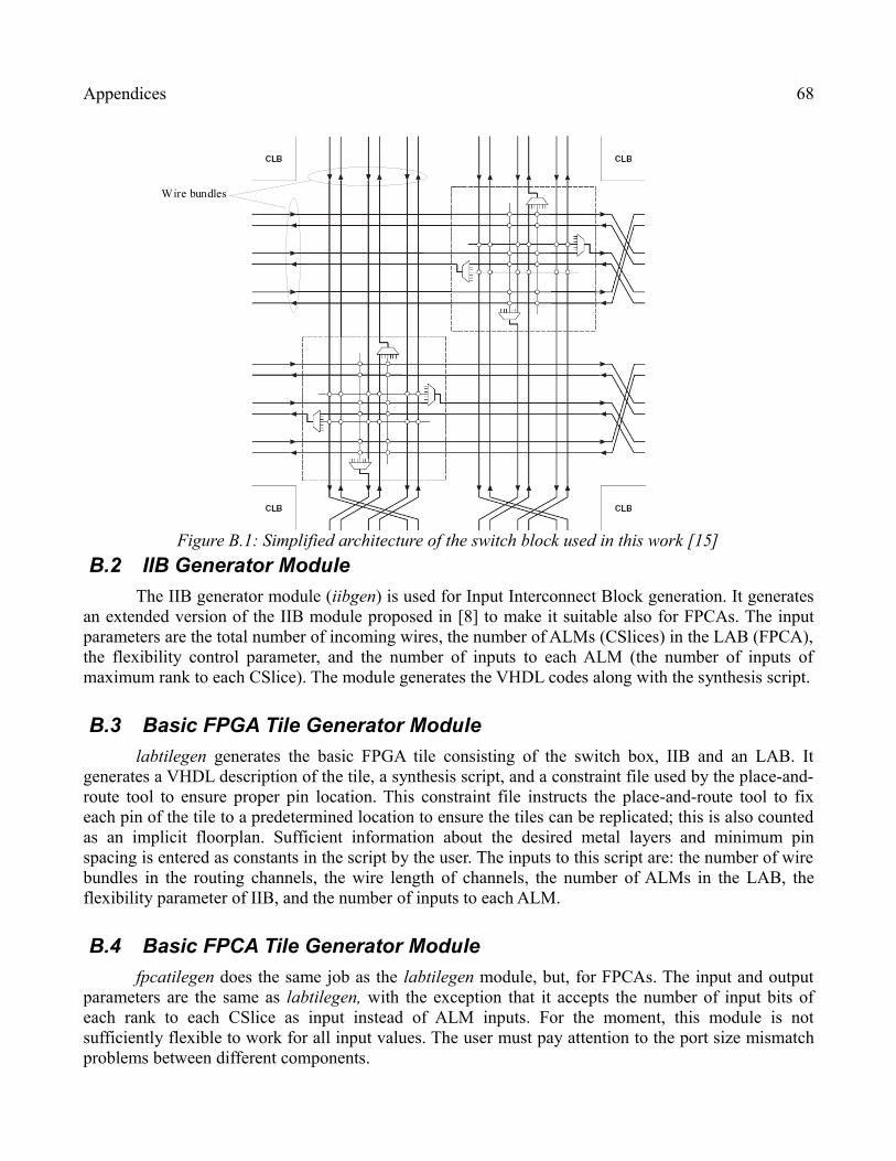
Appendices 68
B.2 IIB Generator ModuleThe IIB generator module (iibgen) is used for Input Interconnect Block generation. It generates
an extended version of the IIB module proposed in [8] to make it suitable also for FPCAs. The input parameters are the total number of incoming wires, the number of ALMs (CSlices) in the LAB (FPCA), the flexibility control parameter, and the number of inputs to each ALM (the number of inputs of maximum rank to each CSlice). The module generates the VHDL codes along with the synthesis script.
B.3 Basic FPGA Tile Generator Modulelabtilegen generates the basic FPGA tile consisting of the switch box, IIB and an LAB. It
generates a VHDL description of the tile, a synthesis script, and a constraint file used by the place-and-route tool to ensure proper pin location. This constraint file instructs the place-and-route tool to fix each pin of the tile to a predetermined location to ensure the tiles can be replicated; this is also counted as an implicit floorplan. Sufficient information about the desired metal layers and minimum pin spacing is entered as constants in the script by the user. The inputs to this script are: the number of wire bundles in the routing channels, the wire length of channels, the number of ALMs in the LAB, the flexibility parameter of IIB, and the number of inputs to each ALM.
B.4 Basic FPCA Tile Generator Modulefpcatilegen does the same job as the labtilegen module, but, for FPCAs. The input and output
parameters are the same as labtilegen, with the exception that it accepts the number of input bits of each rank to each CSlice as input instead of ALM inputs. For the moment, this module is not sufficiently flexible to work for all input values. The user must pay attention to the port size mismatch problems between different components.
Figure B.1: Simplified architecture of the switch block used in this work [15]
Wire bundles

Appendices 69
B.5 Shadow Tile GeneratorsThe shadowtilegen modules generate extended versions of the FPCA tile with shadow cluster
capability. They are a modified versions of the fpcatilegen module with the same input parameters; they add the shadow cluster LAB(s) in parallel to the FPCA. These module require modifications in parameterization direction in order to make it work for arbitrary sized shadow cluster.