Embed Size (px)
Citation preview

DESIGN, SIMULATION, FABRICATION, AND CHARACTERISTICS
OF TERAHERTZ METAMATERIAL DEVICES
by
LEE A. BUTLER
SEONGSIN M. KIM, COMMITTEE CHAIR
PATRICK KUNG
PATRICK LECLAIR
A THESIS
Submitted in partial fulfillment of the requirements
for the degree of Master of Science
in the Department of Electrical and Computer Engineering
in the Graduate School of
The University of Alabama
TUSCALOOSA, ALABAMA
2012

Copyright Lee A. Butler 2012
ALL RIGHTS RESERVED

ii
ABSTRACT
In recent years metamaterials have been extensively researched and show strong potential
to improve many devices. Metamaterials offer significant advantages over conventional
materials because their properties depend mainly on geometrical design rather than composition.
This important property allows metamaterials to be geometrically scaled such as to operate in
any desired spectral range. Specifically, implementation of metamaterials into devices targeted to
operate in the terahertz regime could greatly improve fields such as chemistry, biology, security,
and medicine.
In this work, terahertz metamaterials have been studied and novel devices have been
designed and demonstrated. In particular, this work is focused mainly on metamaterial structures
designed to absorb incident radiation. These absorber devices show promise for use in areas such
as imaging and interference reduction applications. Both narrow-band and broadband absorber
devices have been designed using simulations and fabricated using standard photolithography
and electron deposition techniques.

iii
DEDICATION
This thesis is dedicated to everyone who supported me throughout my academic career.
Especially, I wish to dedicate it to my family and friends whose constant aid and encouragement
has allowed me to accomplish this goal.

iv
LIST OF ABBREVIATIONS AND SYMBOLS
THz Terahertz (1x10¹²
Hz)
PDE Partial Differential Equation
FEA Finite Element Analysis
DOF Degree(s) of Freedom
SRR Split-Ring Resonator
EC-SRR Edge-Coupled Split-Ring Resonator
ERR Electric Ring Resonator
Electric Field Intensity in Volts per meter (V/m)
Magnetic Field Intensity in Amperes per meter (A/m)
Electric Flux Density in Coulombs per square meter (C/m2)
Magnetic Flux Density in Webers per square meter (Wb/m2)
Electric Current Density in Amperes per square meter (A/m2)
Electric Charge Density in Coulombs per cubic meter (C/m3)
Complex Poynting Vector

v
ACKNOWLEDGMENTS
I would like to thank all professors, colleagues, family, and friends who have helped me
in any way with this research work. I wish to express the utmost gratitude to my advisors, Dr.
Margaret Kim and Dr. Patrick Kung for all of their support and guidance throughout my graduate
study. They have provided me with much direction and guidance which has allowed me to
perform the research necessary for the compilation of this thesis.
I also wish to thank Dr. Patrick LeClair for his time, support of my work, and willingness
to serve on my thesis committee. Additionally, I would like to thank my colleagues, Shawn and
Eli, for providing experimental data necessary for this work. Finally, I want to thank my family
and friends for all of their support throughout the assembly of this work.
vi
CONTENTS
ABSTRACT ................................................................................................ ii
DEDICATION ........................................................................................... iii
LIST OF ABBREVIATIONS AND SYMBOLS ...................................... iv
ACKNOWLEDGMENTS ........................................................................... v
LIST OF TABLES ................................................................................... viii
LIST OF FIGURES ................................................................................... ix
1 INTRODUCTION .................................................................................1
1.1 Project Goal and Thesis Outline ......................................................2
2 METAMATERIALS .............................................................................3
2.1 Engineering Electromagnetic Response ..........................................5
2.2 Split-Ring Resonator ........................................................................6
2.3 THz Metamaterial Absorber ..........................................................13
2.3.1 Simulation of Previously Reported Designs .........................15
2.3.2 Proposed Design: Polarization-Insensitive THz Absorber ...19
2.3.3 Broadband THz Absorber .....................................................22
3 FEA SIMULATIONS ..........................................................................24
3.1 Simulation Method.........................................................................24
3.2 Results ............................................................................................26
3.2.1 Normal Incidence Tests ........................................................26

vii
3.2.2 Polarization Sensitivity Tests ................................................30
3.2.3 Broad Band Absorption Tests ...............................................33
4 EXPERIMENTAL MEASUREMENTS .............................................41
4.1 Device Fabrication .........................................................................41
4.2 Measurement Technique ................................................................43
4.3 Results ............................................................................................44
4.3.1Normal Incidence Tests .........................................................45
4.3.2 Polarization Sensitivity Tests ................................................47
5 CONCLUSIONS AND FUTURE WORK ..........................................49
5.1 Summary ........................................................................................49
5.2 Future Work ...................................................................................49
REFERENCES ..........................................................................................51

viii
LIST OF TABLES
2.1 Split-ring resonator geometrical parameters ........................................10
2.2 Geometrical parameters for absorber similar to that proposed
by H. Tao ...................................................................................................15
3.1 Geometrical parameters for proposed polarization-insensitive
absorber ......................................................................................................27
3.2 Geometrical parameters for proposed broadband absorbers ................34
3.3 Geometrical parameters for proposed eight-ring broadband
absorbers ....................................................................................................38
4.1 Geometrical parameters for fabricated absorber arrays .......................45

ix
LIST OF FIGURES
2.1 Right-handed and left-handed triplet systems........................................4
2.2 Combinations of material permittivity and permeability .......................6
2.3 Circular split-ring resonator ...................................................................7
2.4 Split-ring resonator behavior and equivalent circuit ..............................8
2.5 Transmission spectrum of EC-SRR .....................................................11
2.6 Electric response of EC-SRR structure and current in both rings .......12
2.7 Metamaterial THz absorber unit cell ...................................................14
2.8 Absorption spectra with electric and magnetic response at
resonance....................................................................................................16
2.9 Metamaterial THz absorber unit cell similar to that proposed
by Y. Ma et al.............................................................................................17
2.10 Absorption spectra of closed ring absorber structures with
electric responses at resonance ..................................................................18
2.11 Surface current on the closed rings of square-ring and
circular-ring absorbers ...............................................................................19
2.12 Polarization-insensitive THz metamaterial absorber structure ..........20
2.13 Various field polarization angles incident upon a THz
metamaterial structure ................................................................................21
2.14 Rotations to test absorber sensitivity to various incidence
angles .........................................................................................................21
2.15 Designed structure for THz metamaterial broadband absorber .........22
2.16 Circular ring design structure for THz metamaterial
broadband absorber ....................................................................................23

x
3.1 The finite element method process of meshing and refining ...............25
3.2 Absorption spectra with electric and magnetic response at
resonance....................................................................................................28
3.3 Effect of dielectric layer thickness on absorption ................................29
3.4 Electric and magnetic field vectors solved using FEA at
normal incidence ........................................................................................30
3.5 Absorption spectra resulting from variance in polarization angles .....31
3.6 Absorption spectra resulting from various incidence angles ...............32
3.7 Absorption spectra of square-ring and circular-ring broadband
absorbers ....................................................................................................35
3.8 Square eight-ring broadband absorber structure ..................................36
3.9 Circular eight-ring broadband absorber structure ................................37
3.10 Absorption spectra of eight-ring broad band absorbers .....................39
4.1 Metamaterial absorber fabrication process ..........................................42
4.2 Optical microscope images of fabricated metamaterial absorber
array ...........................................................................................................43
4.3 Experimental setup for study of metamaterial absorbers .....................44
4.4 Experimental absorption spectra of fabricated absorber arrays ...........46
4.5 Absorption spectrum of Y’ showing discrepancy correction ..............47
4.6 Absorption spectra resulting from experimental measurements
of polarization variations ...........................................................................48

1
CHAPTER 1
INTRODUCTION
Metamaterials have a strong potential to greatly impact the electromagnetic response of
many materials and devices. First proposed by V.G. Veselago in 1968 as “left-handed
substances”, metamaterials are constructed such that electromagnetic properties are exhibited
which do not occur in nature. Research focusing on the electromagnetic response of
metamaterials has generated fascinating devices such as invisibility cloaks and superlenses [1-4].
These devices are able to be realized due to un-natural material behavior which results from
engineering material characteristics. Metamaterials can be characterized by effective complex
permittivity ( ) ( ) ( ) and permeability ( ) ( ) ( ). By carefully
constructing materials to take advantage of the ability to adjust ( ) and ( ), it is possible to
create metamaterials which exhibit properties such as backward wave propagation and negative
index of refraction, ( ) [5, 6]. Much unlike conventional materials, electromagnetic
properties of metamaterials strongly depend on the structures themselves, much more so than
material chemical composition. Typically, metamaterials are composed of periodic arrays of
metallic elements designed to exhibit resonant behavior at some desired frequency. Thus, one
important feature of metamaterials is their ability to be scaled geometrically in order to achieve
desired electromagnetic responses in various frequency ranges. Consequently, metamaterial
devices have been realized and demonstrated in spectral ranges from radio and microwave up to
infrared and near-optical [7-10].

2
In this work, the focus is on electromagnetic properties of metamaterials in the terahertz
(THz) regime. The terahertz radiation spectrum lies in between radio frequencies and optical
frequencies at 0.1-10 THz (1 THz = 1x10¹²
Hz). This translates to a wavelength range of 30 μm -
3 mm. Until recently, little work has been done in the THz range due to its difficulty to produce
and manipulate. But many substances have a strong response at terahertz frequencies. Thus, there
is a wide variety of applications for devices utilizing THz radiation [11-14] which are promising
tools for matter characterization. Unlike radiation in the X-ray frequency range, terahertz
radiation is not harmful. This property makes it ideal for use in applications such as non-invasive
medical imaging and security screening. Additionally, this low-energy, non-ionizing radiation, is
able to penetrate non-conductive materials with low water content, rendering them transparent in
the THz range. For this reason, THz radiation can non-invasively and accurately characterize
tissues, teeth, DNA, weapons, explosives, and potentially epithelial cancer [15-20]. Thus,
terahertz spectroscopy shows promise to greatly impact fields such as chemistry, biology,
security, and medicine.
1.1 Project Goal and Thesis Outline
The goal of this work was to design, develop, fabricate, and test novel metamaterial
devices. The primary focus was the development and fabrication of novel THz metamaterial
absorbers. In Chapter 2, a concise theory of metamaterials is given which is the basis for the
subsequent THz absorber designs. Chapter 3 introduces the finite element analysis solution
method used for device development and presents simulation data. The experimental
measurement technique and results are presented in Chapter 4. Finally, the conclusion and future
work are covered in Chapter 5.
3
CHAPTER 2
METAMATERIALS
Metamaterials have potential to open up a whole new class of tools and instruments as
the fundamental units of extraordinary devices such as superlenses, invisibility cloaks, sensors,
filters, and antennas to name a few. The basic theory of modern metamaterials was first proposed
in a well-known paper by V.G. Veselago in 1968 but such materials were not realized until the
end of the 20th
century. Here, a brief overview of metamaterial theory is presented. The familiar
governing expressions for all electromagnetic waves, Maxwell’s equations, are expressed here in
the differential form [21]:
(Faraday’s Law of Induction) (2.1)
(Gauss’s Law for Magnetism) (2.2)
(Ampere’s Circuital Law) (2.3)
(Gauss’s Law) (2.4)
It is also worth noting that these expressions contain information expressing the conservation of
charge in a relation known as the equation of continuity:
(Conservation of Charge) (2.5)
The electromagnetic constitutive relationships in simple matter are the following:
= ε
= μ

4
= σ
where σ is the medium, or material, conductivity usually expressed in Siemens per meter (S/m).
These expressions must be satisfied for all electromagnetic fields at all points in space and for all
points in time. Also, these expressions along with relations (2.1) – (2.4) exhibit the importance of
electric permittivity and magnetic permeability to the electromagnetic response of metamaterials.
The vast majority of naturally occurring materials are characterized by positive permittivity and
permeability values ( >0, >0). One exception is plasma, which can exhibit negative
permittivity. Also, metals can exhibit negative permittivity at optical frequencies and some
ferromagnetic materials may exhibit negative permeability at microwave frequencies.
Metamaterials, however, can be constructed to exhibit negative permittivity and negative
permeability. If permittivity and permeability are simultaneously negative (ε < 0, μ < 0), the
result is a negative index of refraction (n < 0). In this case, the material is known as left-handed
media and the phenomenon of backward wave propagation is exhibited. Shown in Figure 2.1,
this is one significant property of metamaterials that makes possible such devices as superlenses.
Figure 2.1 (left) Right-handed triplet system: Poynting vector and wave vector in same direction.
(right) Left-handed media: Poynting vector and wave vector in opposite directions
5
2.1 Engineering Electromagnetic Response
Due to the importance of effective material permittivity and permeability, we may now
explore how to control these parameters in order to develop novel devices. In electromagnetism,
permittivity is defined to be the ability of a material to polarize in response to an external electric
field. Simply put, it is a measure of how well a material transmits an electric field. Similarly,
permeability is defined to be the ability of a material to magnetize in response to an external
magnetic field. We now know that in order to develop such interesting devices as perfect lenses
and invisibility cloaks, precise control of permittivity and permeability values must be achieved.
Consider the diagram in Figure 2.2 showing each possible combination of permittivity and
permeability. It turns out that negative effective permittivity may be achieved by a very simple
periodic array of metallic wires. Achieving negative permeability, however, is a bit more
complicated requiring, for instance, an array of split-ring resonators. These resonators are the
fundamental element in D. Schurig’s cloaking design and will be discussed in the following
section. The response of these split-ring resonator arrays (as with any metamaterial structure) is
highly dependent on size, shape, and electromagnetic wave polarization.

6
Figure 2.2 Every combination of material permittivity and permeability, and some properties of
each
2.2 Split-Ring Resonator
It is well-known that a time-varying magnetic field imposed upon a metallic ring induces
an electrical current. This phenomenon was established by Michael Faraday in the nineteenth
century. The self-inductance of such a closed metallic ring has been found to be
[ (
) ] (2.6)
where r is the radius of the ring and d is the diameter of the ring. For all practical ratios of r/d,
the expression (2.6) results in self-inductance values L ≥ μ0r. Ultimately, the magnetic
susceptibility is given as
| |
(2.7)

7
Thus, these expressions reveal that no configuration of closed metallic rings can result in a LC
resonance or a negative value for effective permeability. LC resonance can be achieved by
loading the ring with a capacitor. This arrangement, first proposed by S.A. Schelkunoff, results
in a magnetic polarizability expressed as
(
)
(2.8)
where ω0 is the resonance frequency of the equivalent LC circuit formed by the closed ring and
the capacitor. The resonance frequency can be calculated by
√ or
√ .
By quick examination of expression (2.8), it is easy to see that just above resonance frequency
the polarizability becomes negative (large negative value). Thus, it can be expected that an
arrangement of closed metallic rings loaded with capacitors will produce a negative effective
permeability just above the resonance frequency. But fabrication of such a structure designed for
operation at microwave and higher frequencies would be difficult. This challenge can be
overcome by replacing the lumped capacitance with a distributed capacitance. Known as the
split-ring resonator (SRR), this configuration was first proposed by J.B. Pendry in 1999 [22] and
is shown in Figure 2.3 (depth not shown).
Figure 2.3 Circular split-ring resonator proposed by J.B. Pendry in 1999

8
Pendry’s SRR is able to exhibit resonances at wavelengths that are much larger than the ring
diameters. This structure also allows the possibility to fabricate a large series of small rings using
common photo-etching techniques which can provide resonances and large negative values of
effective permeability. Also, this structure can be scaled down to operate at infrared and optical
frequencies. The particular design proposed by Pendry is known as an “edge-coupled SRR” or
“EC-SRR” which consists of two concentric metallic rings printed on a microwave circuit board.
Having two rings (as opposed to only one), allows this structure to obtain a higher capacitance
which results in a stronger resonance. When the EC-SRR is excited by a time-varying magnetic
field polarized perpendicular to the plane of the rings, the splits on each ring cause electric
current to flow from one ring to the other across the spacing between them. Thus, the spacing (or
slot) between concentric rings serves as a distributed capacitance. Additionally, if the electric
field is polarized perpendicular to the gaps in the rings, a capacitance is formed in the gaps.
Figure 2.4 shows the behavior of the edge-coupled split-ring resonator as well as the EC-SRR
equivalent circuit.
Figure 2.4 Split-ring resonator behavior (left) and SRR equivalent circuit model (right)
9
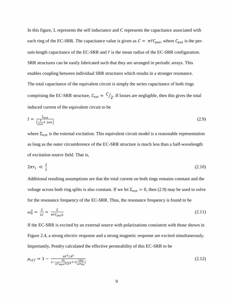
In this figure, L represents the self inductance and C represents the capacitance associated with
each ring of the EC-SRR. The capacitance value is given as , where is the per-
unit-length capacitance of the EC-SRR and is the mean radius of the EC-SRR configuration.
SRR structures can be easily fabricated such that they are arranged in periodic arrays. This
enables coupling between individual SRR structures which results in a stronger resonance.
The total capacitance of the equivalent circuit is simply the series capacitance of both rings
comprising the EC-SRR structure, ⁄ . If losses are negligible, then this gives the total
induced current of the equivalent circuit to be
(
)
(2.9)
where is the external excitation. This equivalent circuit model is a reasonable representation
as long as the outer circumference of the EC-SRR structure is much less than a half-wavelength
of excitation source field. That is,
(2.10)
Additional resulting assumptions are that the total current on both rings remains constant and the
voltage across both ring splits is also constant. If we let , then (2.9) may be used to solve
for the resonance frequency of the EC-SRR. Thus, the resonance frequency is found to be
(2.11)
If the EC-SRR is excited by an external source with polarizations consistent with those shown in
Figure 2.4, a strong electric response and a strong magnetic response are excited simultaneously.
Importantly, Pendry calculated the effective permeability of this EC-SRR to be
(
) (2.12)

10
where A is the lattice parameter and ρ is the per unit length resistance.
In order to demonstrate the operation of circular split-ring resonators, simulations have
been carried out on the EC-SRR structure of Figure 2.3. The geometrical parameters used for the
simulations are shown and the values are given in Table 2.1.
Table 2.1 Split-ring resonator geometrical parameters
EC-SRR Geometrical Parameters
r (μm) w (μm) g (μm) d (μm) thickness (μm)
15 4 2.44 3 1
When this configuration is excited, surface currents are forced to flow on the edge-coupled rings
and the electric field induces a capacitance. Thus, a strong LC response is given at a specific
frequency, ω0, such that
√ (2.13)
The transmission spectrum resulting from the response of the simulated EC-SRR structure is
shown in Figure 2.5. The transmission is obtained from a two-port system power flow using the
following relation
(2.14)

11
Figure 2.5 Transmission spectrum of circular EC-SRR. Resonance is at 1.16 THz
This EC-SRR was simulated using the finite-element method which will be discussed in the
following chapter. The rings were modeled as lossless copper with frequency-independent
conductivity = 6 x 10⁷ S/m. The SRR was placed in free-space. The dip in transmission
intensity indicates a resonance at f0 = 1.16 THz which corresponds to the LC resonance. The
electric and magnetic responses in the edge-coupled ring structure are more clearly visible by
making use of the finite element analysis solutions to view the electric field and current. The
normal electric field and current is shown in Figure 2.6 for a non-resonance frequency as well as
for the resonance frequency.
0
0.1
0.2
0.3
0.4
0.5
0.6
0.7
0.8
0.9
1
0.50 0.70 0.90 1.10 1.30 1.50 1.70 1.90
Tran
smis
sion
(x100%
)
Frequency (THz)

12
Figure 2.6 Electric response of the EC-SRR structure (top) and current in both rings (bottom) for
a non-resonance frequency and at resonance frequency
Thus, at non-resonance frequency (in this case 0.7 THz) no capacitance is formed in the structure
so no electric response is exhibited. Additionally, it is interesting to note that the small surface
currents are directed in a closed loop about both rings (counterclockwise along the inside and
clockwise along the outside). On the other hand, at resonance frequency (1.16 THz) a
capacitance is formed in the ring gaps as well as in the area between rings resulting in a strong
electric response visible at the top right of Figure 2.6. Also at resonance frequency, notice that
the current in the structure is consistent with that shown in Figure 2.4 with the current highly
concentrated on the outer ring and directed clockwise.

13
2.3 THz Metamaterial Absorber
Quite recently, it has been shown that by clever adjustment of ( ) and ( ), resonant
metamaterials which are highly absorbent may be realized [23, 24]. These spectrally selective
absorbers show strong potential for use as the fundamental elements in sensor/detector devices
such as thermal imagers and explosives detectors as well as interference reduction applications.
More specifically, these devices would prove especially beneficial in the THz regime for
imaging purposes in the fields of biology and medicine. Metamaterials offer a means of
developing tools and instruments for use in the THz range where few electromagnetically
responsive materials occur in nature. In order to obtain high absorption, transmission (T(ω)) and
reflection (R(ω)) must be simultaneously minimized. The frequency-dependent absorption is
defined by A(ω) = 1-T(ω)-R(ω). Thus, if T(ω0) ≈ R(ω0) ≈ 0 then the desired high absorption
A(ω0) ≈ 1 may be obtained at some resonance frequency, ω0. At any other frequency, the
absorption will be very small (A ≈ 0). First proposed and demonstrated at microwave frequencies
by N.I. Landy in 2008, metamaterial absorbers consist of two metallic layers separated by a
dielectric spacer (some designs include a substrate) [25, 26]. These absorbers allow the incident
electric and magnetic fields to be simultaneously absorbed. Consider the absorber unit cell
structure shown in Figure 2.7.

14
Figure 2.7 Metamaterial THz absorber unit cell
The effective permittivity and permeability are able to be tuned by adjusting the electric and
magnetic responses independently. Adjustment of the electric response is achieved by
geometrical variations of the top metallic layer known as the electric ring resonator (ERR) [27].
Based on the aforementioned split-ring resonator, the ERR is designed to exhibit only an electric
response by making use of “plates” to form a capacitance. The magnetic response can be
adjusted by changing the spacing between metallic layers since the incident magnetic field
couples to these layers. It was mentioned earlier that in order for reflection to be ≈ 0, the
effective impedance of the structure must be matched to that of free-space. Since the back layer
of this structure is a continuous ground plane, zero transmission (T(ω) = 0) is ensured for all
THz frequencies. Thus, for this configuration only incidence and reflection contribute to the total
field. In order for the impedance of the structure to match free-space impedance, permittivity and
permeability must be carefully adjusted such that
√
(2.15)

15
This means that maximum absorption will occur when the relative effective permittivity and
permeability are most nearly equal (ε(ω0) ≈ μ(ω0)).
2.3.1 Simulation of Previously Reported Designs
The configuration shown in Figure 2.7 is the basic novel design proposed by H. Tao et al in
2008. This design effectively exhibits near-perfect absorption at THz frequencies. In order to
demonstrate the performance of this metamaterial absorber and to validate the accuracy of our
simulation method, the design of Figure 2.7 was simulated. The design was modeled with very
similar parameters to that tested by H. Tao et al. The metallic layers were modeled as copper and
the dielectric layer was modeled as polyimide. Table 2.2 displays geometrical parameters for
absorbers to target three different frequencies.
Table 2.2 Geometrical parameters for absorber similar to that proposed by H. Tao
Design
Geometrical Parameters
d (μm) wr (μm) wc (μm) g (μm) h1 (μm)
Metallic Layer
Thickness (μm)
sep (μm)
A 35 3.5 15 2.5 47 0.2 8.8
B 30 3 13 2 40 0.2 7.7
C 25 2.5 11 1.5 33.5 0.2 7.1
The simulated absorption spectrum for each variation on the design by H. Tao et al is shown in
Figure 2.8. The electric (inset top) and magnetic (inset bottom) responses at resonance are also
shown for this design.

16
Figure 2.8 Absorption spectra with electric response (inset top) and magnetic response (inset
right) at resonance
Thus, designs A, B, and C exhibit absorptions of 99.1%, 99.1%, and 99.2%, respectively.
These near-unity absorptions occur at center frequencies 1.15 THz, 1.327 THz, and 1.57 THz for
designs A, B, and C, respectively. The absorption peaks offer a full-width-at-half-maximum
(FWHM) from 0.07 THz to 0.11 THz making this absorber structure ideal for spectrally-
selective imaging applications. An additional metamaterial absorber design of great importance
to this work is a structure similar to that of Figure 2.7. Shown in Figure 2.9, this slight variation
on a design proposed by Y. Ma et al in 2011 consists of a square closed ring structure and a
ground plane separated by a dielectric layer.
0.00
0.10
0.20
0.30
0.40
0.50
0.60
0.70
0.80
0.90
1.00
0 0.25 0.5 0.75 1 1.25 1.5 1.75 2 2.25
Ab
sorp
tion
(x100%
)
Frequency (THz)
A
B
C

17
Figure 2.9 Metamaterial THz absorber unit cell similar to that proposed by Y. Ma et al
This design is another spectrally selective near-perfect absorber with copper metallic layers and a
polyimide dielectric layer. But the mechanism that produces absorption includes a dipole
resonance along the sides of the square ring, rather than a LC resonance as in the previous
design. This is precisely the property that supports broad-band absorbers developed in this work,
which will be discussed in following sections. As an example of the performance of these
structures, Figure 2.10 shows the absorption spectra of the simulated square-ring design as well
as a very similar circular-ring design. Also shown is the electric field intensity in each ring
(inset) at the resonance frequency. The tested square-ring design has side lengths of 60 µm
which is also the diameter of the tested circular-ring design. Each ring is 2 µm wide and 0.4 µm
thick.

18
Figure 2.10 Absorption spectra of closed ring absorber structures with electric responses (inset)
at resonance
Thus, these two designs exhibit absorptions of 99.6% (square) and 99.1% (circular). These near-
unity absorptions occur at center frequencies 0.881 THz and 1.099 THz for the square-ring and
circular-ring structures, respectively. It is of importance to note the behavior of surface current,
0.00
0.10
0.20
0.30
0.40
0.50
0.60
0.70
0.80
0.90
1.00
0.00 0.20 0.40 0.60 0.80 1.00 1.20 1.40 1.60
Ab
sorp
tion
(x100%
)
Frequency (THz)
0.00
0.10
0.20
0.30
0.40
0.50
0.60
0.70
0.80
0.90
1.00
0.00 0.20 0.40 0.60 0.80 1.00 1.20 1.40 1.60 1.80
Ab
sorp
tion
(x100%
)
Frequency (THz)

19
induced by the incident field, on these absorber structures. The surface current on each closed-
ring absorber structure is shown in Figure 2.11.
Figure 2.11 Surface current on the closed rings of square-ring (left) and circular-ring (right)
absorbers
The red arrows in Figure 2.11 represent the surface current with the arrow size being
proportional to current intensity. Note that the incident field induces surface current in opposite
directions concentrated on the sides of the rings.
2.3.2 Proposed Design: Polarization-Insensitive THz Absorber
For implementation into applications it is highly desirable that absorber structures can
operate using a wide range of incident field polarizations. This functionality improvement would
allow an absorber to perform in a variety of environments and under a variety of conditions. To
achieve this, we designed a metamaterial absorber structure similar to that of Figure 2.7 which
consists of two additional interior “plates”. This new structure is shown in Figure 2.12.
20
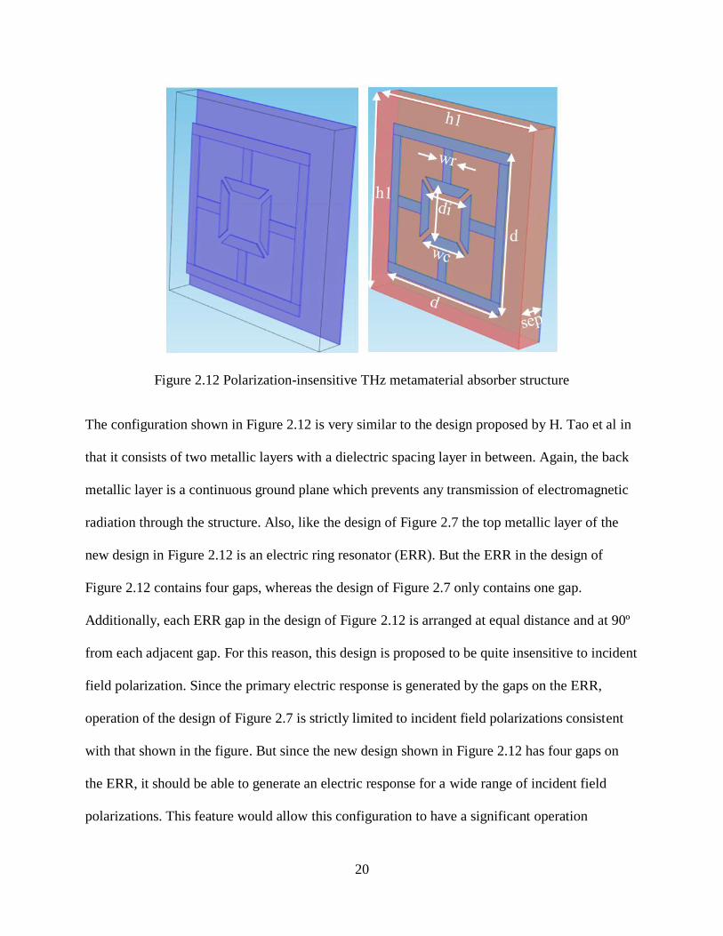
Figure 2.12 Polarization-insensitive THz metamaterial absorber structure
The configuration shown in Figure 2.12 is very similar to the design proposed by H. Tao et al in
that it consists of two metallic layers with a dielectric spacing layer in between. Again, the back
metallic layer is a continuous ground plane which prevents any transmission of electromagnetic
radiation through the structure. Also, like the design of Figure 2.7 the top metallic layer of the
new design in Figure 2.12 is an electric ring resonator (ERR). But the ERR in the design of
Figure 2.12 contains four gaps, whereas the design of Figure 2.7 only contains one gap.
Additionally, each ERR gap in the design of Figure 2.12 is arranged at equal distance and at 90º
from each adjacent gap. For this reason, this design is proposed to be quite insensitive to incident
field polarization. Since the primary electric response is generated by the gaps on the ERR,
operation of the design of Figure 2.7 is strictly limited to incident field polarizations consistent
with that shown in the figure. But since the new design shown in Figure 2.12 has four gaps on
the ERR, it should be able to generate an electric response for a wide range of incident field
polarizations. This feature would allow this configuration to have a significant operation

21
advantage over the earlier design shown in Figure 2.7 since it would not be limited to specific
polarizations of incident radiation. Figure 2.13 and Figure 2.14 display tests which are very
important to the efficient operation of absorbers.
Figure 2.13 Various field polarization angles incident upon a THz metamaterial absorber
Figure 2.14 Rotations to test absorber sensitivity to various incidence angles (a) Rotations about
magnetic field. (b) Rotations about electric field
Insensitivity to incident field polarization (Fig. 2.13) and insensitivity to angle of propagation
(Fig. 2.14) are very important properties that metamaterial absorbers are desired to exhibit.
Efficient absorber performance under conditions of various polarization angles and angles of

22
propagation will allow an absorber structure to be very versatile. Such versatile absorbers could
benefit many sensor/detector devices and interference reduction applications.
2.3.3 Broadband THz Absorber
For many applications, especially interference reduction applications, it may be desired
that absorber structures operate over a wide range of frequencies. Since the mechanism that
causes absorption in the aforementioned structure of Figure 2.9 is dipole resonances rather than
LC resonances, the top rings may be arranged concentrically. One such concentric ring
configuration under study in this work is shown in Figure 2.15.
Figure 2.15 Designed structure for THz metamaterial broadband absorber
23
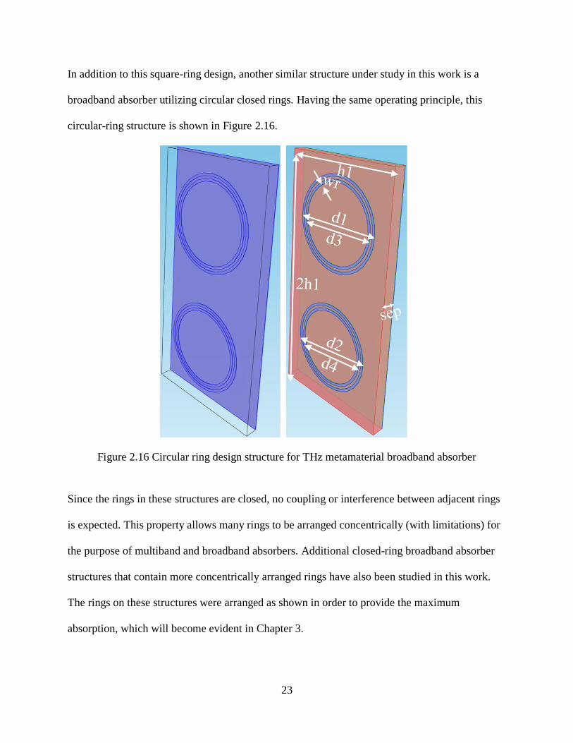
In addition to this square-ring design, another similar structure under study in this work is a
broadband absorber utilizing circular closed rings. Having the same operating principle, this
circular-ring structure is shown in Figure 2.16.
Figure 2.16 Circular ring design structure for THz metamaterial broadband absorber
Since the rings in these structures are closed, no coupling or interference between adjacent rings
is expected. This property allows many rings to be arranged concentrically (with limitations) for
the purpose of multiband and broadband absorbers. Additional closed-ring broadband absorber
structures that contain more concentrically arranged rings have also been studied in this work.
The rings on these structures were arranged as shown in order to provide the maximum
absorption, which will become evident in Chapter 3.

24
CHAPTER 3
FEA SIMULATIONS
Simulation software was used to support the design and development of the metamaterial
devices studied in this work. The software package chosen for this work was COMSOL
Multiphysics [28]. This software makes use of the finite element method to approximate
solutions for Maxwell’s equations. Finite element analysis (FEA) software was selected due to
its ability to model more complex geometries than other methods such as the finite difference
method. Subsequent device fabrication was based on results from the simulated solutions.
3.1 Simulation Method
The finite element method was used to predict and confirm the behavior of metamaterial
structures. This solving technique is a powerful method of approximating solutions to partial
differential equations (PDE’s). Finite element analysis (FEA) is capable of simulating the
behavior of very complex structures. The finite element method was first used to solve
mechanical deformation and stress problems. Eventually, FEA was adapted to approximate
solutions to Maxwell’s equations for electromagnetic fields analysis. First, the structure under
study is constructed (3-dimensional). Boundary conditions are imposed on each domain of the
structure based on the desired study. The finite element method then divides the structure into
many smaller, simpler elements in a process known as meshing. The number of elements

25
produced can be adjusted to achieve the desired solution resolution (with limitations). Adjacent
elements are connected at nodes as shown in Figure 3.1.
Figure 3.1 The finite element method process of meshing and refining
The desired field expressions to be approximated are interpolated by polynomials over each
element. The result of this interpolation is a large set of algebraic equations to be solved
simultaneously. The collection of elements and nodes results in a finite number of degrees-of-
freedom (DOF) to be solved over, whereas continuous structures have an infinite number of
DOF. Unknown field quantities over each element are found from the approximated solutions.
The resulting approximated solutions can then be viewed for interpretation. Using the solutions,
many other field quantities may also be calculated (power, energy, etc.).

26
3.2 Results
Finite element analysis simulations were carried out on all aforementioned absorber
structures that we designed. Presented first are the simulation results for the structure of Figure
2.12 excited by a plane wave incident normal to the structure surface. Next, the simulation
results are shown for various incident field polarization configurations on the structure of Figure
2.12. Shown last are the simulation results for the broadband absorber structures of Figure 2.15
and 2.16 excited by a plane wave at normal incidence.
3.2.1 Normal Incidence Tests
To prove matched performance with the design of Figure 2.7 at normal incidence, three
variations on the design of Figure 2.12 have been modeled and simulated (X, Y, Z) using the
finite element method. The two metallic layers (highlighted purple in Fig. 2.12) were modeled as
copper with frequency independent conductivity = 6 x 10⁷ S/m. Each of the metallic layers was
modeled 400 nm thick. The dielectric layer between metallic layers (highlighted red in Fig. 2.12)
was modeled as polyimide with = 6.7 x 10⁻¹⁶
S/m, ε = 3.0 + i0.03, and μ = 1. The real
component of the dielectric permittivity was obtained through experimental reflectance
measurements and the imaginary component was found experimentally using ellipsometry. The
absorber of Figure 2.12 was modeled in a free-space medium as the unit cell of an infinite array
of absorbers in both directions along the plane perpendicular to the direction of propagation.
Table 3.1 displays geometrical parameters for the three simulated absorbers of Figure 2.12.

27
Table 3.1 Geometrical parameters for proposed polarization-insensitive absorber
Design
Geometrical Parameters
d (μm) di (μm) wr (μm) wp (μm) h1 (μm)
Metallic Layer
Thickness (μm)
sep (μm)
X 56 20 4 21 75 0.4 9.4
Y 50 18 3.5 19 67 0.4 8.5
Z 44 15.5 3 16.5 59 0.4 7.1
The values displayed in Table 3.1 have been found to provide maximum absorption at normal
incidence. The simulated absorption spectrum for each variation on the design Figure 2.12 is
shown in Figure 3.2. Since this structure provides T(ω) = 0, the absorption (or absorbance) can
be calculated simply by
( ) ( ) (3.1)
Reflection, ( ), is defined to be
( ) ( ) ( )
(3.2)
The electric (inset top) and magnetic (inset bottom) responses at resonance are also shown in
Figure 3.2.

28
Figure 3.2 Absorption spectra with electric response at resonance (inset top) and magnetic
response at resonance (inset bottom)
Thus, designs X, Y, and Z exhibit absorptions of 99.9%, 99.9%, and 99.7%, respectively. These
near-unity absorptions occur at center frequencies 0.796 THz, 0.888 THz, and 1.004 THz for
designs X, Y, and Z, respectively. These absorption peaks offer a FWHM from 0.045 THz to
0.06 THz making this absorber structure even more attractive for spectrally-selective imaging
applications than the design of Figure 2.7.
In order to optimize these structures to obtain such high absorptions as shown in Figure
3.2, the exact parameters must be found that provide a match of permittivity and permeability
which in turn provides an impedance match to free-space. The parameter most sensitive to
absorption levels is the spacing distance between metallic layers (dielectric layer thickness). A
simulated sweep on this spacing (called sep here) was performed for each of the variations on the
design of Figure 2.12. The results from design Y are shown in Figure 3.3 revealing a glimpse of
the sensitivity of these structures to dielectric spacer thickness.
0
0.1
0.2
0.3
0.4
0.5
0.6
0.7
0.8
0.9
1
0 0.25 0.5 0.75 1 1.25 1.5
Ab
sorp
tion
(x100%
)
Frequency (THz)
X
Y
Z
29
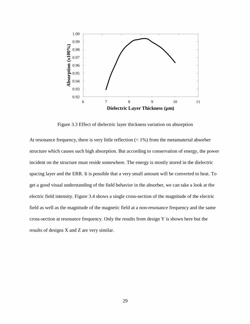
Figure 3.3 Effect of dielectric layer thickness variation on absorption
At resonance frequency, there is very little reflection (< 1%) from the metamaterial absorber
structure which causes such high absorption. But according to conservation of energy, the power
incident on the structure must reside somewhere. The energy is mostly stored in the dielectric
spacing layer and the ERR. It is possible that a very small amount will be converted to heat. To
get a good visual understanding of the field behavior in the absorber, we can take a look at the
electric field intensity. Figure 3.4 shows a single cross-section of the magnitude of the electric
field as well as the magnitude of the magnetic field at a non-resonance frequency and the same
cross-section at resonance frequency. Only the results from design Y is shown here but the
results of designs X and Z are very similar.
0.92
0.93
0.94
0.95
0.96
0.97
0.98
0.99
1.00
6 7 8 9 10 11
Ab
sorp
tion
(x100%
)
Dielectric Layer Thickness (µm)

30
Figure 3.4 Electric and magnetic field vectors which were solved using FEA at normal incidence.
Electric (a) and magnetic (c) field vectors at non-resonance frequency (0.4 THz). Electric (b) and
magnetic (d) field vectors at resonance frequency (0.888 THz)
The red arrows in Figure 3.4 represent the scattered electric or magnetic field intensity. At non-
resonance frequency, the solution results in a large amount of reflection (> 99%) which is visible
by the high density of red arrows in Figure 3.4 (a) and (c). But at resonance frequency, the
solution reveals that the reflected electric field and magnetic field (and thus reflected power) are
extremely small (< 1%) which is visible by the lack of red arrows in Figure 3.4 (b) and (d).
3.2.2 Polarization Sensitivity Tests
One important feature of the design of Figure 2.12 is that it is proposed to be insensitive
to incident field polarization. To test this hypothesis, finite element simulations were carried out

31
for two additional polarization angles (15o and 45
o). The rotation angles of polarization were
performed as shown in Figure 2.13. The particular simulations used to test polarization angles
were performed using the optimized structure of design Y. To test polarization insensitivity, only
three angles of incident polarization were simulated. But due to both vertical and horizontal
symmetry, any subsequent polarization rotation of 90o will result in the same solution and thus,
the same absorption spectrum. This property is in stark contrast to the design of Figure 2.12
which would result in an extremely low absorption upon rotation of 90° from the incident field
polarization shown in Figure 2.7. Figure 3.5 shows a comparison of the absorption spectra
resulting from the two additional polarization angles.
Figure 3.5 Absorption spectra resulting from variance in polarization angles
Demonstrating the versatility of this absorber structure, these polarization angles each result in
absorptions greater than 99%. This finding confirms that the design of Figure 2.12 would be
ideal for applications in spectrally selective imaging as well as applications to reduce
interference. But these simulations were all performed with the incident radiation at normal
0.00
0.10
0.20
0.30
0.40
0.50
0.60
0.70
0.80
0.90
1.00
0 0.2 0.4 0.6 0.8 1 1.2 1.4 1.6
Ab
sorp
tion
(x100%
)
Frequency (THz)
0° / n·90°
15°
45°

32
incidence (0o). To further test the insensitivity of the design of Figure 2.12 to incident radiation,
computer simulations were performed on design Y for various radiation oblique incidence
angles. To ensure a robust testing procedure, the structure was tested for incidence angles
relative to the electric field polarization as well as relative to the magnetic field polarization as
shown in Figure 2.14. Simulations were carried out on design Y for three additional incidence
angles (15°, 25°, and 45°) relative to the electric field as well as the magnetic field. Figure 3.6
shows a comparison of the absorption spectra resulting from the three additional incidence
angles for each case.
0.00
0.10
0.20
0.30
0.40
0.50
0.60
0.70
0.80
0.90
1.00
0.00 0.20 0.40 0.60 0.80 1.00 1.20 1.40 1.60
Ab
sorp
tion
(x100%
)
Frequency (THz)
0°
15°
25°
45°
(a)

33
Figure 3.6 Absorption spectra resulting from various incidence angles. (a) From rotations about
incident electric field and (b) from rotations about incident magnetic field
Incidence angles varied in both directions result in absorptions > 96% for all tested angles which
allows this design to be an excellent candidate for applications in interference reduction as well
as spectrally selective imaging. Despite a very slight frequency shift for 45° about the electric
field, according to simulations the design of Figure 2.12 is able to obtain high absorption (near
unity) for a wide range of incidence angles. In addition to polarization and incidence angle
insensitivity, the design of Figure 2.12 has distinct important advantages over other absorber
designs. This design is very thin (6-9 μm) and any substrate can be selected since the continuous
ground plane provides zero transmission. Also, it is mechanically flexible allowing it to bend and
wrap around objects which could likely be required in many applications.
3.2.3 Broad Band Absorption Tests
In order to develop an optimized design and demonstrate the performance of broadband
absorbers, the designs of Figure 2.15 and Figure 2.16 have been modeled and simulated using
0.00
0.10
0.20
0.30
0.40
0.50
0.60
0.70
0.80
0.90
1.00
0.00 0.20 0.40 0.60 0.80 1.00 1.20 1.40 1.60
Ab
sorp
tion
(x100%
)
Frequency (THz)
0°
15°
25°
45°
(b)

34
FEA. The two metallic layers (highlighted purple in Fig. 2.15 and Fig. 2.16) were modeled as
copper with conductivity = 6 x 10⁷ S/m. Again, each of the metallic layers was modeled
400nm thick. The dielectric layer between metallic layers (highlighted red in Fig. 2.15 and Fig.
2.16) was modeled as polyimide with = 6.7 x 10⁻¹⁶
S/m, ε = 3.0 + i0.03, and μ = 1. The
absorber structures were modeled in a free-space medium as described before. Table 3.2 displays
geometrical parameters for the simulated broad band absorbers of Figure 2.15 and Figure 2.16.
Table 3.2 Geometrical parameters for proposed broadband absorbers
Geometrical Parameters
d1 (μm) d2 (μm) d3 (μm) d4 (μm) wr (μm) h1 (μm)
Metallic Layer
Thickness (μm)
75 71 67 63 2 100 0.4
The simulated absorption spectra are shown in Figure 3.7 for various dielectric layer thicknesses
(sep). Again, due to the presence of a ground plane, there is no transmission through the structure
at THz frequencies so equations (3.1) and (3.2) are used to calculate absorption.
35
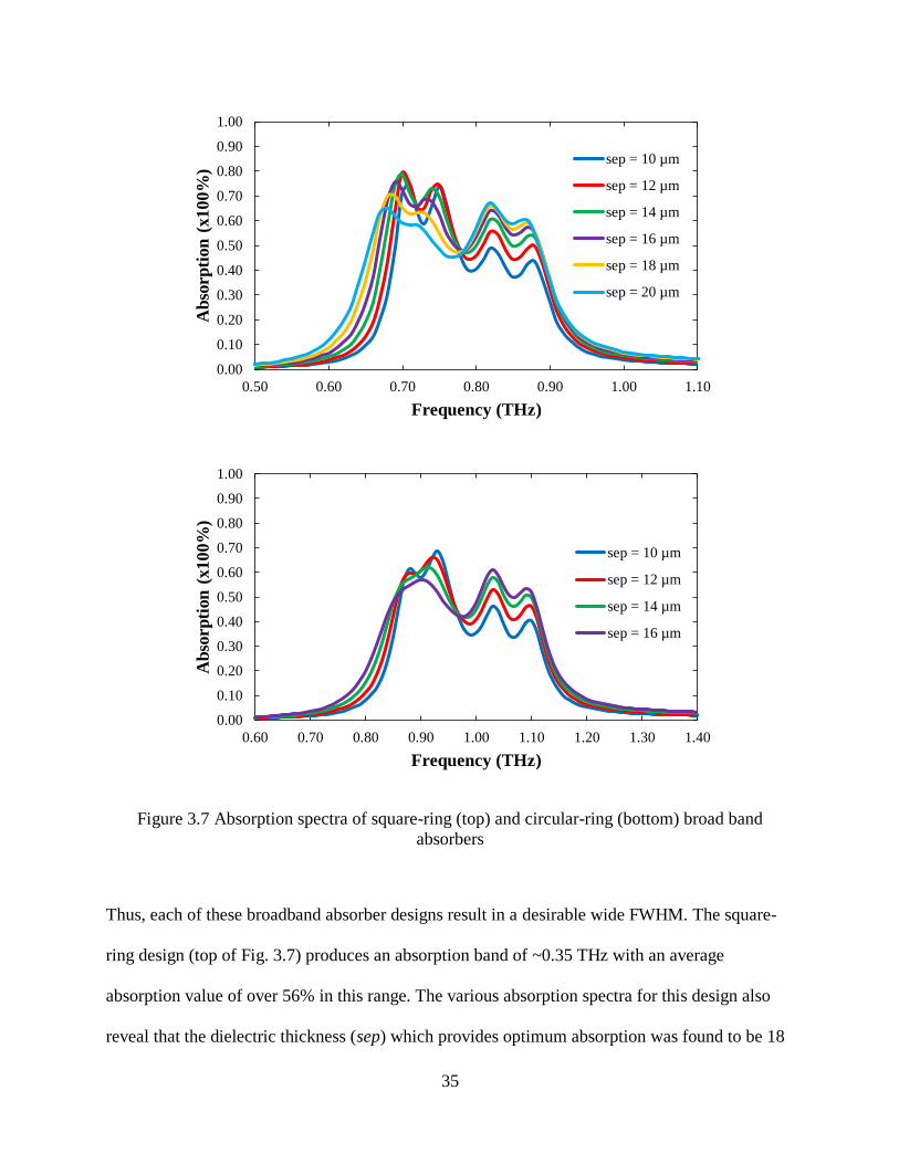
Figure 3.7 Absorption spectra of square-ring (top) and circular-ring (bottom) broad band
absorbers
Thus, each of these broadband absorber designs result in a desirable wide FWHM. The square-
ring design (top of Fig. 3.7) produces an absorption band of ~0.35 THz with an average
absorption value of over 56% in this range. The various absorption spectra for this design also
reveal that the dielectric thickness (sep) which provides optimum absorption was found to be 18
0.00
0.10
0.20
0.30
0.40
0.50
0.60
0.70
0.80
0.90
1.00
0.50 0.60 0.70 0.80 0.90 1.00 1.10
Ab
sorp
tion
(x100%
)
Frequency (THz)
sep = 10 µm
sep = 12 µm
sep = 14 µm
sep = 16 µm
sep = 18 µm
sep = 20 µm
0.00
0.10
0.20
0.30
0.40
0.50
0.60
0.70
0.80
0.90
1.00
0.60 0.70 0.80 0.90 1.00 1.10 1.20 1.30 1.40
Ab
sorp
tion
(x100%
)
Frequency (THz)
sep = 10 µm
sep = 12 µm
sep = 14 µm
sep = 16 µm

36
µm. The circular-ring design (bottom of Fig. 3.7) produces an absorption band of ~0.3 THz with
an average absorption level of over 49% in this range. Additionally, the various absorption
spectra for this design shows that the dielectric thickness (sep) which provides optimum
absorption was found to be 14 µm. The performance of each design is desirable for use in many
applications, especially interference reduction applications.
Additional broadband absorber structures, very similar to those of Figure 2.15 and Figure
2.16, were designed and developed with the intention to increase the absorption band width.
These additional structures (Figure 3.8 and Figure 3.9) contain eight closed rings, both square
and circular, as opposed to four rings as in the previous designs.
Figure 3.8 Square eight-ring broadband absorber structure

37
Figure 3.9 Circular eight-ring broadband absorber structure
Again, finite element simulations were first carried out on these structures to study the
electromagnetic response and optimize the performance of the absorber configurations. Table 3.3
shows the geometrical parameters of the eight-ring structures. The naming convention for the
geometrical parameters is consistent with that shown in Figure 2.15 and Figure 2.16.

38
Table 3.3 Geometrical parameters for proposed eight-ring broadband absorbers
Geometrical Parameters
d1
(μm)
d2
(μm)
d3
(μm)
d4
(μm)
d5
(μm)
d6
(μm)
d7
(μm)
d8
(μm)
wr
(μm)
h1
(μm)
Metallic
Layer
Thickness
(μm)
75 71 67 63 59 55 51 47 2 100 0.4
The simulated absorption spectra for the eight-ring structures are shown in Figure 3.10 for
various dielectric layer thicknesses (sep). Once again, equations (3.1) and (3.2) are used to
calculate absorption.
39
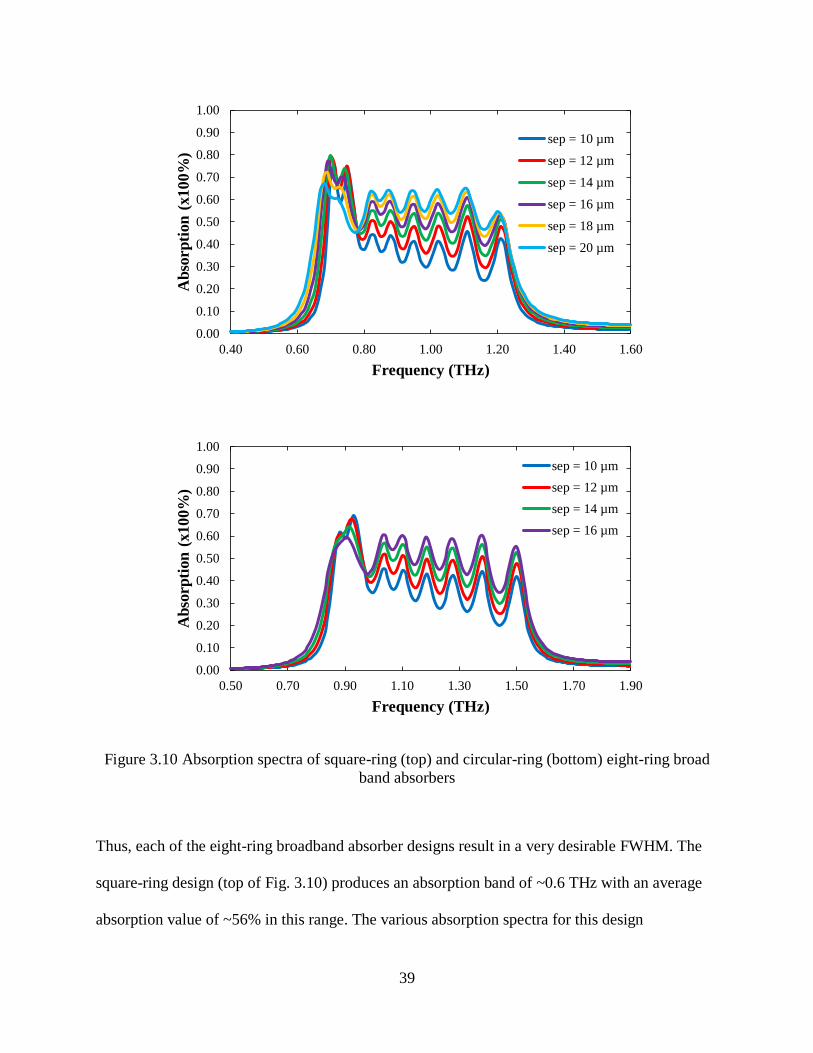
Figure 3.10 Absorption spectra of square-ring (top) and circular-ring (bottom) eight-ring broad
band absorbers
Thus, each of the eight-ring broadband absorber designs result in a very desirable FWHM. The
square-ring design (top of Fig. 3.10) produces an absorption band of ~0.6 THz with an average
absorption value of ~56% in this range. The various absorption spectra for this design
0.00
0.10
0.20
0.30
0.40
0.50
0.60
0.70
0.80
0.90
1.00
0.40 0.60 0.80 1.00 1.20 1.40 1.60
Ab
sorp
tion
(x100%
)
Frequency (THz)
sep = 10 µm
sep = 12 µm
sep = 14 µm
sep = 16 µm
sep = 18 µm
sep = 20 µm
0.00
0.10
0.20
0.30
0.40
0.50
0.60
0.70
0.80
0.90
1.00
0.50 0.70 0.90 1.10 1.30 1.50 1.70 1.90
Ab
sorp
tion
(x100%
)
Frequency (THz)
sep = 10 µm
sep = 12 µm
sep = 14 µm
sep = 16 µm
40
demonstrates that the dielectric thickness (sep) which provides optimum absorption was found to
be 20 µm. The circular-ring design (bottom of Fig. 3.10) produces an absorption band of ~0.71
THz with an average absorption level of over 50% in this range. Also, the various absorption
spectra for this design shows that the dielectric thickness (sep) which provides optimum
absorption was found to be 16 µm. Additionally, the performance of each eight-ring design is
even more desirable for use in applications than the previous four-ring design due to wider
absorption bands without compromising the absorption levels. Of course, however, both four-
ring and eight-ring broadband absorbers have advantages and disadvantages which must be
accounted for when implementing these devices into applications. For instance, some
applications may not require absorption bands as wide as those provided by the eight-ring
designs. In such a case, the four-ring absorbers may be more desirable due to more ease of
fabrication. Furthermore, the work with these particular broadband absorbers suggests that the
addition of more concentric closed rings, with limitations, would increase the width of the
absorption band.

41
CHAPTER 4
EXPERIMENTAL MEASUREMENTS
Metamaterial THz absorbers have been fabricated based on the finite element simulation
data obtained and displayed in the previous chapter. Absorbers structures were fabricated using
the geometrical parameters which were found, through simulations, to provide the optimum
absorption. The fabricated absorber arrays were then tested experimentally. In this chapter, the
fabrication process as well as the experimental measurement technique is described. Lastly,
results from the experimental measurements are presented and discussed.
4.1 Device Fabrication
The metamaterial absorber arrays were fabricated using typical photolithographic and
electron beam evaporation techniques. First, using electron beam deposition a copper ground
plane of appropriate thickness was evaporated onto a 250 µm-thick silicon wafer. A polyimide
separation layer of appropriate thickness (found using simulation data) was then spun onto the
ground plane. A diagram showing the absorber fabrication process is shown in Figure 4.1.

42
Figure 4.1 Metamaterial absorber fabrication process
The resulting structure was subsequently cured in a vacuum oven. Next, a ~0.8 µm-thick layer of
positive photoresist was spun on top of the polyimide layer. This photoresist layer was then soft
baked. A photomask containing the ERR or closed-ring designs was then aligned over the soft-
baked wafer. Next, the masked configuration was briefly exposed to ultraviolet radiation. The
ERR patterns were then able to be developed, clearing away the exposed photoresist. Again
using electron beam evaporation, a layer of appropriately thick copper was evaporated onto the
structure to form the ERR array. Finally, the structure was sonicated in acetone in order to
remove the remaining photoresist. Optical microscope images of the fabricated ERR arrays are
shown in Figure 4.2.
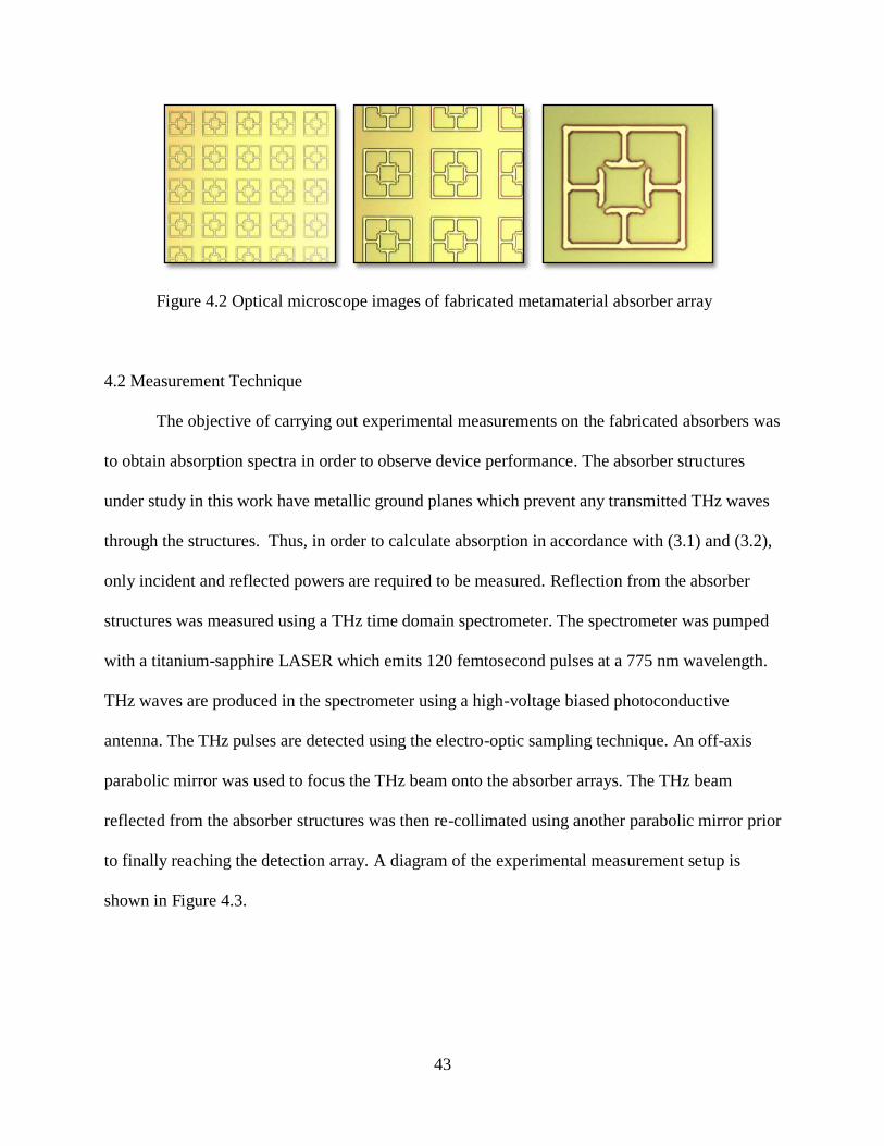
43
Figure 4.2 Optical microscope images of fabricated metamaterial absorber array
4.2 Measurement Technique
The objective of carrying out experimental measurements on the fabricated absorbers was
to obtain absorption spectra in order to observe device performance. The absorber structures
under study in this work have metallic ground planes which prevent any transmitted THz waves
through the structures. Thus, in order to calculate absorption in accordance with (3.1) and (3.2),
only incident and reflected powers are required to be measured. Reflection from the absorber
structures was measured using a THz time domain spectrometer. The spectrometer was pumped
with a titanium-sapphire LASER which emits 120 femtosecond pulses at a 775 nm wavelength.
THz waves are produced in the spectrometer using a high-voltage biased photoconductive
antenna. The THz pulses are detected using the electro-optic sampling technique. An off-axis
parabolic mirror was used to focus the THz beam onto the absorber arrays. The THz beam
reflected from the absorber structures was then re-collimated using another parabolic mirror prior
to finally reaching the detection array. A diagram of the experimental measurement setup is
shown in Figure 4.3.

44
Figure 4.3 Experimental setup for study of metamaterial absorbers
4.3 Results
Experimental measurements, using a reflection-mode time domain spectrometer, were
carried out on several selected fabricated absorber arrays. First presented are some absorption
spectra from both aforementioned narrow-band absorber designs (Fig. 2.7 and Fig. 2.12), which
demonstrate operability. Shown next are absorption spectra resulting from geometrical variations
on the absorber structure of Figure 2.12. Presented last are absorption spectra displaying the
effect of incident field polarization configurations on the absorber design of Figure 2.12.

45
4.3.1 Normal Incidence Tests
To demonstrate the performance of the fabricated absorber arrays, experimental
measurements were carried out with slight modifications on the previously mentioned absorber
designs. These modified designs are denoted by B’, Y’, and Z’. It is important to note that due to
deposition limitations, the metallic layers of the fabricated absorber arrays are 200 nm thick.
Also due to fabrication limitations, the polyimide layer deposited to produce the following
results was 3.5 μm thick. The geometrical parameters of these fabricated absorber devices are
displayed in Table 4.1.
Table 4.1 Geometrical parameters for fabricated absorber arrays
Geometrical Parameters
Design of Figure 2.7
Design d (μm) wr (μm) wc (μm) g (μm) h1 (μm)
Metallic Layer
Thickness (μm)
sep (μm)
B’ 30 3 11 2 40 0.2 3.5
Design of Figure 2.12
Design d (μm) di (μm) wr (μm) wp (μm) h1 (μm)
Metallic Layer
Thickness (μm)
sep (μm)
Y’ 50 18 3.5 13 67 0.2 3.5
Z’ 44 15.5 3 10 59 0.2 3.5

46
The experimental absorption spectra for the fabricated absorber arrays are shown in Figure 4.4.
The experimental spectra are plotted together with the simulated spectra obtained from finite
element analysis.
Figure 4.4 Experimental absorption spectra of fabricated absorber arrays
Notice that the measured spectra closely match that of the simulated spectra, having only a slight
discrepancy of resonance frequency. In this case the simulated absorbers were modeled with
polyimide permittivity ε = 3.5 + i0.03. Figure 4.5 shows that this discrepancy may be corrected
by modeling the polyimide layer with permittivity ε = 3.0 + i0.03.
0.00
0.10
0.20
0.30
0.40
0.50
0.60
0.70
0.80
0.90
1.00
0.00 0.50 1.00 1.50 2.00
Ab
sorp
tion
(x100%
)
Frequency (THz)
B'
Y'
Z'
B' (simulated)
Y' (simulated)
Z' (simulated)

47
Figure 4.5 Absorption spectrum of Y’ showing discrepancy correction
This result is precisely the reason that all previous simulations modeled the polyimide spacer
layer with ε = 3.0 + i0.03. Together, the results of Figure 4.4 and Figure 4.5 demonstrate that the
fabricated absorber arrays are indeed highly absorbent and spectrally selective, having
absorptions near the expected levels and very near the anticipated frequencies of simulated
models. Thus, the fabricated devices show strong potential for use in many detector/sensor
applications. It is expected that these devices would achieve near-unity absorption if they were
fabricated with the optimum geometrical parameters.
4.3.2 Polarization Sensitivity Tests
Experimental measurements were also performed on a selected array of the fabricated
absorbers in order to test the important property of polarization sensitivity. This test was
performed by rotating the absorber array, about its center, relative to the incident field
polarization at three angles (0°, 15°, and 45°). The polarization variations were tested on a
modification on design Y, with sep = 20 µm. The absorption spectra resulting from these
0.00
0.10
0.20
0.30
0.40
0.50
0.60
0.70
0.80
0.90
1.00
0.40 0.60 0.80 1.00 1.20 1.40
Ab
sorp
tion
(x100%
)
Frequency (THz)
Y'
Y' (simulated
ε = 3 + i0.03)

48
experimental measurements are shown in Figure 4.6 which also indicates normal incidence
polarization configuration and subsequent rotation.
Figure 4.6 Absorption spectra resulting from experimental measurements of polarization
variations
Although the absorption is seen to decrease upon varying the incident field polarization
configuration, the amount is very small so the absorber still operates at acceptable levels and at
the same resonance frequency. Again, the device could demonstrate less discrepancy from
simulation if the fabricated absorber geometrical parameters were more closely matched. Even
though the absorber device did not perform near perfection as anticipated, the performance and
versatility does show promise for use in many detector/sensor applications.
0.00
0.10
0.20
0.30
0.40
0.50
0.60
0.70
0.80
0.90
1.00
0.70 0.75 0.80 0.85 0.90 0.95 1.00
Ab
sorp
tion
(x100%
)
Frequency (THz)
0°
15°
45°
E
k

49
CHAPTER 5
CONCLUSIONS AND FUTURE WORK
5.1 Summary
In this work, metamaterial absorber devices have been designed, simulated, fabricated,
and characterized. The structure of Figure 2.12 was designed to be thin, flexible, and insensitive
to incident field polarization and propagation angle. Finite element analysis simulations were
used to optimize the absorption and confirm that the device is highly insensitive to incident field
polarization and angle of propagation. Absorber devices were fabricated using standard
photolithography and electron beam deposition techniques. Although experimental
measurements did not produce ideal results, the obtained results demonstrated the operability and
versatility of the device. The structures of Figure 2.15 and Figure 2.16 were designed to produce
broad absorption spectra. Finite element analysis simulations were also performed on these
structures to optimize absorption strength and spectra width. The simulated solutions show that
these broadband absorbers indeed produce broad absorption spectra, but at the cost of absorption
strength.
5.2 Future Work
This work leaves much room for improvement upon metamaterial absorbers. The
development, fabrication, and characterization presented here have laid a solid foundation to
build upon. Many detector/sensor applications exist for which metamaterial absorbers would
50
improve. For example, it is agreed by many researchers that narrow-band metamaterial absorber
devices show potential for use as fundamental detection elements in imaging applications.
Improvement upon the groundwork performed in this study could significantly benefit the
practicality of such applications. Also, broadband absorber devices show strong potential to be
used in interference reduction applications to neglect unwanted frequencies. Increasing spectra
width and absorption, although seemingly difficult, would certainly enhance the usefulness of
such devices and provide great applicability. Any advancements in the metamaterial absorbers
presented in this work could potentially benefit many scientific areas including chemistry,
biology, security, and medicine.
51
REFERENCES
[1] J.B. Pendry “Negative Refraction Makes a Perfect Lens”, Physical Review Letters, vol.
85, no. 18, pp. 3966-3969, 2000
[2] J.B. Pendry, D. Schurig, D.R. Smith, “Controlling Electromagnetic Fields”, Science, vol.
312, iss. 5781, pp. 1780-1782, 2006
[3] W. Cai, U.K. Chettiar, A.V. Kildishev, V.M. Shalaev, “Optical cloaking with
metamaterials”, Nature Photonics, vol. 1, pp. 224-227, 2007
[4] P. Alitalo, S. Tretyakov, “Electromagnetic cloaking with metamaterials”, Materials
Today, vol. 12, iss. 3, pp. 22-29, 2009
[5] V. G. Vesalago. “The Electrodynamics of Substances with Simultaneously Negative
Values of ε and μ”, Soviet Physics Uspekhi, vol. 10, no. 4, pp. 509-514, 1968
[6] R.A. Shelby, D.R. Smith, S. Schultz, “Experimental Verification of a Negative Index of
Refraction”, Science, vol. 292, no. 5514, pp. 77-79, 2001
[7] D. Schurig, J. J. Mock, B. J. Justice, S. A. Cummer, J. B. Pendry, A. F. Starr, and D. R.
Smith, “Metamaterial Electromagnetic Cloak at Microwave Frequencies”, Science, vol.
314, pp. 977-980, 2006
[8] A. A. Houck, J. B. Brock, I. L. Chuang, “Experimental Observations of a Left-Handed
Material That Obeys Snell’s Law”, Physical Review Letters, vol. 90, no. 13, pg. 137401,
2003
[9] H. Chen, L. Ran, J. Huangfu, X. Zhang, K. Chen, T. M. Grzegorczyk, J.A. Kong, “Left-
handed materials composed of only S-shaped resonators”, Physical Review E, vol. 70, iss.
5, pg. 057605, 2004
[10] B. Kante, D. Germain, A. de Lustrac, “Experimental demonstration of non-magnetic
metamaterial cloak at microwave frequencies”, Physical Review B, vol. 80, pg. 201104,
2009
[11] B. Ferguson, X. Zhang, “Materials for terahertz science and technology”, Nature
Materials, vol. 1, iss. 1, pp. 26-33, 2002
52
[12] B. Fischer, M. Hoffmann, H. Helm, G. Modjesch, P.U. Jepsen, “Chemical recognition in
terahertz time-domain spectroscopy and imaging”, Semiconductor Science and
Technology, vol. 20, iss. 7, pp. S246-S253, 2005
[13] P.H. Siegel, “Terahertz Technology”, IEEE Transactions on Microwave Theory and
Techniques, vol. 50, no. 3, pp. 910-918, 2002
[14] J.S. Melinger, N. Laman, and D. Grischkowsky, “The underlying terahertz vibrational
spectrum of explosives solids”, Applied Physics Letters, vol. 93, iss. 1, pg. 011102, 2008
[15] R.M. Woodward, V.P. Wallace, D.D. Arnone, E.H. Linfield, M. Pepper, “Terahertz
Pulsed Imaging of Skin Cancer in the Time and Frequency Domain”, Journal of
Biological Physics, vol. 29, iss. 2, pp. 257-261, 2003
[16] T. Loffler, T. Bauer, K.J. Siebert, H.G. Roskos, A. Fitzgerald, S. Czash, “Terahertz dark-
field imaging of biomedical tissue”, Optics Express, vol. 9, pp. 616-621, 2001
[17] K. Humphreys, J.P. Loughran, M. Gradziel, W. Lanigan, T. Ward, J.A. Murphy, C.
O’Sullivan, “Medical applications of Terahertz Imaging: a Review of Current
Technology and Potential Applications in Biomedical Engineering”, Engineering in
Medicine and Biology Society, pp. 1302-1305, 2004
[18] A.G. Davies, A.D. Burnett, W. Fan, E.H. Linfield, J.E. Cunningham, “Terahertz
spectroscopy of explosives and drugs”, Materials Today, vol. 11, iss. 3, pp. 18-26, 2008
[19] D.L. Woolard, E.R. Brown, A.C. Samuels, J.O. Jensen, T. Globus, B. Gelmont, M.
Wolski, “Terahertz-Frequency Remote-Sensing of Biological Warfare Agents”,
Microwave Symposium Digest, vol. 2, pp. 763-766, 2003
[20] S. Dexheimer, “Terahertz Spectroscopy: Principles and Applications”, CRC Press, Boca
Raton, FL, 2008
[21] R.F. Harrington, “Time-Harmonic Electromagnetic Fields”, McGraw Hill, New York,
NY, 1961
[22] J. B. Pendry, A. J. Holden, D. J. Robbins, and W. J. Stewart, “Magnetism from
Conductors and Enhanced Nonlinear Phenomena”, IEEE Transactions on Microwave
Theory and Techniques, vol. 47, no. 11, pp. 2075-2084, 1999
[23] N.I. Landy, S. Sajuyigbe, J.J. Mock, D.R. Smith, W.J. Padilla, “A Perfect Metamaterial
Absorber”, Physical Review Letters, vol. 100, pg. 207402, 2008
[24] H.Tao, N.I. Landy, C.M. Bingham, X. Zhang, R.D. Averitt, W.J. Padilla, “A
metamaterial absorber for the terahertz regime: Design, fabrication and characterization”,
Optics Express, vol. 16, pp. 7181-7188, 2008
53
[25] H. Tao, C.M. Bingham, A.C. Strikwerda, D. Pilon, D. Shrekenhamer, N.I. Landy, K. Fan,
X. Zhang, W.J. Padilla, R.D. Averitt, “Highly flexible wide angle of incidence terahertz
metamaterial absorber: Design, fabrication, and characterization”, Physical Review B,
vol. 78, pg. 241103, 2008
[26] H. Tao, C.M. Bingham, D. Pilon, K. Fan, A.C. Strikwerda, D. Shrekenhamer, W.J.
Padilla, X. Zhang, R.D. Averitt, “A dual band terahertz metamaterial absorber”, Journal
of Physics D: Applied Physics, vol. 43, iss. 22, pg. 225102, 2010
[27] W.J. Padilla, M.T. Aronsson, C. Highstrete, M. Lee, A.J. Taylor, R.D. Averitt,
“Electrically resonant terahertz metamaterials: Theoretical and experimental
investigations”, Physical Review B, vol. 75, iss. 4, pg. 041102, 2007
[28] COMSOL Multiphysics 4.1, COMSOL, Inc.