Embed Size (px)
Citation preview

February 4.-5.2004 ESTEC
Design of High Speed Pipeline ADC
Estec February 4-5, 2004
Väinö [email protected]
Electric Circuit Design LaboratoryHelsinki University of Technology

February 4.-5.2004 ESTEC
Outline• Background• Resources• Specifications• Architecture
– ADC– Clock generation
• Phase 1 test chip– Schematics & Simulations

February 4.-5.2004 ESTEC
Background
• Wideband high speed ADCs required for satellite comminications
• Target to design and implement high speed ADC to feed poly phase filter
• Project started: 12/2002• Closing: First half of 2005

February 4.-5.2004 ESTEC
Resources
• ECDL (Väinö Hakkarainen, Mikko Aho, Jaana Riikonen, Kari Halonen)– ADC design– Calibration
• VTT (Arto Rantala, David Comes Martins, Markku Åberg)– Clock generation & skew calibration
• Nokia (Paavo Kosonen, Tom Ahola)– Measurements

February 4.-5.2004 ESTEC
Target Specifications
• Resolution 9-10 bits• Sample Rate 1.8-2 GS/s• 500 MHz input bandwidth• Monolithic ADC• “Low” power dissipation (<10W)• Target technology: BiCMOS 0.35 µm (SiGe)

February 4.-5.2004 ESTEC
Design Challenges• Clock generator is the most critical block
– Jitter specification– Resolution of the skew correction
• Calibration• Area and power dissipation must be controlled• Measurements @ 2 GS/s Sample rate• Very tight schedule
– Test chip + final version within two years

February 4.-5.2004 ESTEC
Architecture (1)• Pipeline topology most suitable
– Resolution– Calibration– Double-sampling– Time-interleaving
• DLL based clock generation– Lower jitter than in PLLs– Skew calibration achievable
February 4.-5.2004 ESTEC
Architecture (2)• Time-interleaved
parallel pipeline• Low-jitter clock
generator with skew correction
• Digital calibration of channel gain and offset mismatch

February 4.-5.2004 ESTEC
Architecture -Summary
Architecture Monolithic Time Interleaved Pipeline Resolution 9-10 bits Sample Rate 1.8-2 GS/s Number of Channels 24 Channel Clock Rate 75-85 MHz Calibration Digitally with FPGA Sample Clock Generation Adjustable DLL Technology 0.35-µm BiCMOS (SiGe)

February 4.-5.2004 ESTEC
Pipeline ADC

February 4.-5.2004 ESTEC
Double-Sampling (1)• Shared opamp between two pipeline fingers
– Working in opposite clock phases
• Lower power dissipation but,• Memory effect could cause error
– Faster settling required

February 4.-5.2004 ESTEC
Double-Sampling (2)
• Φ1 and Φ2 in opposite phases
• Bottom plate sampling utilized (Φ1
’
Φ2’)
• ΦTOT operating at 2*fs => Skew insensitivity

February 4.-5.2004 ESTEC
Clock Generation• Lowest jitter with external crystal oscillator
– ENOB = 8 bits @ 1 GHz requires σa < 0.5 ps• Adjustable DLL• Skew between
channels minimizedwith calibration
• Very careful layoutdesign
February 4.-5.2004 ESTEC
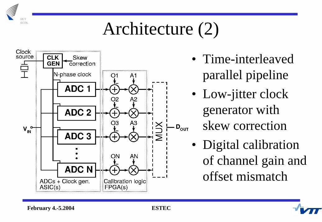
Jitter Minimization• DLL achieves a lower jitter than PLL
– Also favorable for time-interleaved ADC
• Thermal jitter of a DLL ~ N2 (N = length of DLL)– High-frequency external crystal oscillator– Dividers after DLL to get 20 clocks
• Additional jitter from on-chip components minimized
• If not enough, additional steps– Combination from several clock signals

February 4.-5.2004 ESTEC
Clock Skew Calibration
• Digitally controlled delay adjustment circuits after the clock division– Coarse adjustment required before division
• Skew calibration with PC• Possible skew measurement strategies
– Phase difference with inverse FFT– Phase difference from sine-fit test– In time domain from a ramp input signal to ADC

February 4.-5.2004 ESTEC
Clock Generator (1)• A combined divider and delay-locked loop
(DLL) clock generator• Supply controlled delay elements (cross-coupled
inverters)• Digital counters at the output of the DLL
provides 12 evenly spaced phases• A skew calibration is applied to the output
phases
February 4.-5.2004 ESTEC
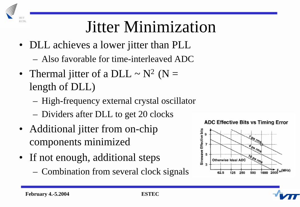
Clock Generator (2)
• A high frequency external clock is phased with a short DLL
• Clock phases detected by Edge Compiner
• Output spectrum is analyzed to find out the best calibration code

February 4.-5.2004 ESTEC
Specifications -Phase 1 Test Chip• Sampling frequency
– Single channel : 75-100 MS/s– Number of channels : 4– Total : 300-400 MS/s
• Resolution– Stage : 1.5 bits+ 2 bits (flash)– Number of stages : 8+1– Total : 10 bits
• Test DLL Blocks– Driving ADC– Jitter determination

February 4.-5.2004 ESTEC
Layout Phase 1Test Chip
•Two skew-insensitive double-sampled ADC fingers•Test DLLs•Area: 1.7 x 6.8 mm2
•Sent to process June/03, Received Nov./03. •Measurements running
February 4.-5.2004 ESTEC
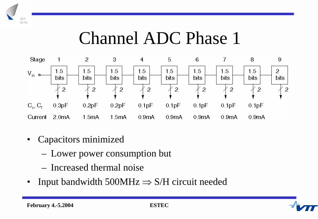
Channel ADC Phase 1
• Capacitors minimized– Lower power consumption but– Increased thermal noise
• Input bandwidth 500MHz ⇒ S/H circuit needed

February 4.-5.2004 ESTEC
OpAmp
M1 M2
M7 M8
M9
Vin+ Vin-
Vout- Vout+
Vcmfb
Vb1
CL CL
M5 M6
Q1 Q2
Vb2
Vb3
•BiCMOS telescopic OTA•Relative low current consumption (max 2mA)•Bipolars used to achieve enough gain•Pure CMOS requires two stage OpAmp

February 4.-5.2004 ESTEC
SimulationsOpAmp
A0 71 dBGBW 1385 MHzVin,pp 0.5VPM 72.4o
• 1st stage OpAmp

February 4.-5.2004 ESTEC
Dynamic Comparator

February 4.-5.2004 ESTEC
Bootstrapped Input Switch
•Insensitive to input voltage amplitude•Used in first stage as sampling switch

February 4.-5.2004 ESTEC
SimulationsClock generator

February 4.-5.2004 ESTEC
SimulationsUncalibrated 4-Channel
fin 72.8 MHzfclk 80 MHzftot 360 MHzSFDR 30.5 dBSNDR 30.5 dBENOB 4.8 bits

February 4.-5.2004 ESTEC
SimulationsCalibrated 4-Channel
fin 72.8 MHzfclk 80 MHzftot 360 MHzSFDR 64.1 dBSNDR 57.1 dBENOB 9.1 bits

February 4.-5.2004 ESTEC
SimulationsSummary
4-chan uncalib. 4-chan calib. 1st 1.5-bit Channel ADC Channel Pair Input Switch
fin 72.8 MHz 72.8 MHz 9.1 MHz 9.1 MHz 9.1 MHz 913 MHzfclk 80 MHz 80 MHz 80 MHz 80 MHz 80 MHz 100 MHz
SFDR 30.5 dB 64.1 dB 72 dB 64 dB 63.5 dB 81 dBSNDR 30.5 dB 57.1 dB 56.5 dB 56.5 dBENOB 4.8 bits 9.1 bits 9.1 bits 9.1 bitsVin,pp -1 dBFS -1 dBFS 0.5 V 0.5 V 0.5 V 0.5 V
Behavioral Transistor level

February 4.-5.2004 ESTEC
Drawbacks
• MPW runs of current BiCMOS 0.35 µm-process stopped => Forced to change vendor
• Problems with PCBs => Measurements delayed• New test chip to process 4/2004• Target tape out of final version moved to
11/2004


![Pipeline ADC with a Nonlinear Gain Stage and Digital ... · Pipeline ADC with a Nonlinear Gain Stage and Digital Correction A Major Qualifying Project ... 2.6 SAR ADC opTology [1]](https://img.dokumen.tips/doc/110x75/5ace65f37f8b9ae2138b4b90/pipeline-adc-with-a-nonlinear-gain-stage-and-digital-adc-with-a-nonlinear-gain.jpg)