Embed Size (px)
Citation preview

Design of an Integrated Electronic Speed Controller for
Compact Robotic Vehicles Benjamin Tefay, Bazle Eizad, Peter Crosthwaite, Surya Singh, Adam Postula
Robotic Aircraft Research Group
School of Information Technology and Electrical Engineering
The University of Queensland, Brisbane 4072
[email protected], {b.eizad, p.crosthwaite, spns, a.postula}@uq.edu.au
Abstract
Adopting a system-on-chip approach, this paper presents an integrated FPGA-based Elec-tronic Speed Control (ESC) for driving brushless DC electric motors. This allows for sensing, computation, and higher control bandwidth than traditional off-the-shelf ESCs (typically 50Hz). In addition to a more compact and flexible pack-age, this provides greater system awareness and facilitates a faster control loop rate, which are useful for agile robotic systems, such as UAVs.
This design has been tested in conjunction with a custom, compact quadrotor system. It provides reduced payload and increased robust-ness compared to traditional controllers.
1 Introduction
Unmanned vehicles, particularly Unmanned Aerial Vehi-cles (UAVs), have the potential to make remote opera-tions cheaper, safer, and more accessible [Meyers et al., 2007]. Urban applications, such as assisting police, fire department and emergency services, require UAVs to be flown in constrained environments. Flying in such spaces presents several challenges, such as noise and collision risks, hence the desire for compact systems with lower speeds and masses.
This cannot be achieved while being slow and passive as urban operations still require high manoeuvrability; thus, the need for efficient motor actuator performance and faster control loop rates so as to exploit non-linear platform characteristics. This is particularly the case for Brushless DC (BLDC) motors as integrated sensing al-lows for variable commutation patterns giving precise control over motor RPM and torque.
This paper develops and analyses a Field Programma-ble Gate Array (FPGA) based Electronic Speed Controller (ESC) that can be integrated into an existing FPGA solu-tion with the addition of supporting motor driving circuits (e.g., high-current MOSFETs in a H-bridge configura-tion). This is integrated into the design of a light (2 kg) semi-autonomous quadrotor (see Figure 1). In compari-son to off-the-shelf ESCs that limit control to 50Hz [Mey-ers et al, 2007] and provide no feedback, this provides improved modularity and system integration and allows for improved control algorithms and fault detection.
Figure 1 Quadrotor platform with FPGA board
2 Electric Motor and ESC Background
Brushless DC motors provide higher power density and efficiency compared to brushed DC motor architectures, but require careful driving and commutation, leading to system complexity [Singh and Singh, 2009]. They are becoming increasingly popular as they are compact in size and have good power density, controllability and efficien-cy while avoiding the maintenance, acoustic noise and electromagnetic interference of brushed DC motors [Torres, 2008; Miller, 1989; Atmel, 2005]. The motors are also continually improving and decreasing in cost due to advances in permanent magnets, structural design and control [Singh and Singh, 2009]. Due to these advantages BLDC motors are the most commonly used motors in UAV technology.
Figure 2 A sensorless BLDC motor
Proceedings of Australasian Conference on Robotics and Automation, 7-9 Dec 2011, Monash University, Melbourne Australia.
Page 1 of 8

Most BLDC motors have three terminals as shown in Figure 2 [Brown, 2002]. These terminals are connected to stator windings (also known as phases) in a Y configura-tion as shown in Figure 3. The centre point of the Y is re-ferred to as the neutral point of the motor. Permanent magnets are positioned on the rotor such that the poles facing the stator alternate between north and south.
Figure 3 Electrical and mechanical model of BLDC
An ESC for a BLDC motor controls the rotation of the motor by selectively energising its phases. When current is driven through the stator windings the moving electric charge interacts with the rotor magnetic field and gener-ates force on the rotor which can cause it to rotate. The controller can operate a BLDC motor like a stepper motor without feedback. However, if the rotor position is known, then the controller can calculate the optimal wind-ings to energize at any point in time to achieve the desired rotation speed and torque more efficiently. Many of the BLDC motors available do not have direct sensing for de-tecting the position of the rotor. However, this infor-mation can be observed by looking at the Back Electro-motive Force (back-EMF). The back-EMF and current within a phase winding must be in phase so as to maxim-ise the amount of positive torque and minimise the amount of negative torque generated. Alternatively, the current and back-EMF can be out of phase by 180 to maximise the amount of negative torque generated. Pro-vided the torque generated is predominately positive or predominately negative, the motor will rotate. Further-more, the shape of the current waveform does not matter provided the back-EMF and current are mostly the same sign (maximising positive torque) or mostly the opposite sign (maximising negative torque) at the same times. If torque is not consistently generated in a single direction the rotor will be accelerated and decelerated reducing ef-ficiency. This is known as cogging torque.
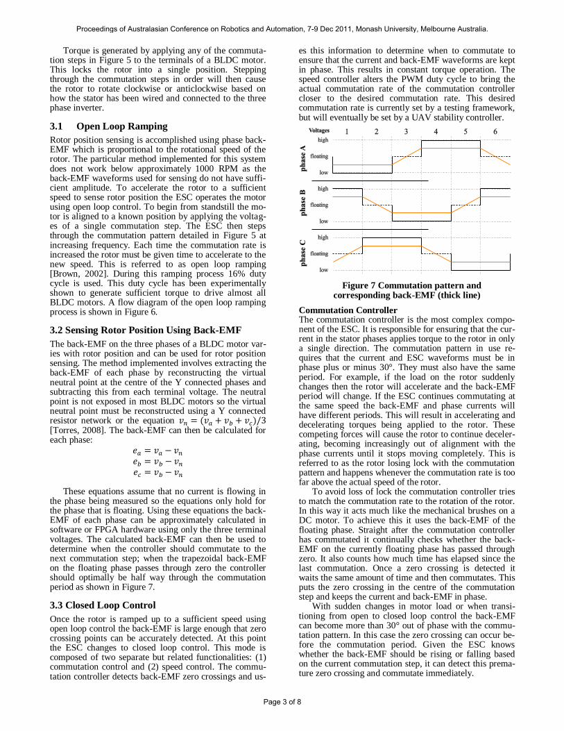
Constant torque operation is by far the most common method of operation [Gamazo-Real et al., 2010] and is applicable to UAVs. To achieve constant torque the cur-rents in the three phases of a BLDC should be trapezoidal and out of phase by 120 . Furthermore, the current and back-EMF within each phase winding should be in phase. This is most commonly achieved by applying a high volt-age to one phase, a low voltage to another phase, and leaving the remaining phase floating.
3 ESC Design and Operation
A three-phase inverter design was chosen to control the BLDC motor terminal voltages. This design uses three MOSFET half-bridges as shown in Figure 4. The common six step commutation pattern shown in Figure 5 is used in
conjunction with this design. Pulse Width Modulation (PWM) is only applied to the low side MOSFETs. The ro-tor position sensing algorithm which has been implement-ed is not affected by the PWM pattern therefore the pat-tern was chosen to reduce switching losses and match the commercial ESCs already in use for ease of comparison.
Figure 4 Three phase voltage inverter connected to BLDC motor
Figure 5 Voltages applied to 3 phases of BLDC mo-tor during commutation pattern
Open Loop Speed Ramping
Commutator
Freeze commutator
Wait for commutation
period
Output next
commutation step to
six MOSFETs
Wait for motor to align
Set PWM duty cycle,
PWM frequency
Set commutation
pattern
Start commutator
Wait for motor to
accelerate to current
commutation rate
Increase commutation
rate
BEMF detectable?
No
Open loop control
Switch to closed loop
control
Open loop control
Yes
Figure 6 Flow diagram of the logic for acceleration using open loop control
Proceedings of Australasian Conference on Robotics and Automation, 7-9 Dec 2011, Monash University, Melbourne Australia.
Page 2 of 8
Torque is generated by applying any of the commuta-tion steps in Figure 5 to the terminals of a BLDC motor. This locks the rotor into a single position. Stepping through the commutation steps in order will then cause the rotor to rotate clockwise or anticlockwise based on how the stator has been wired and connected to the three phase inverter.
3.1 Open Loop Ramping
Rotor position sensing is accomplished using phase back-EMF which is proportional to the rotational speed of the rotor. The particular method implemented for this system does not work below approximately 1000 RPM as the back-EMF waveforms used for sensing do not have suffi-cient amplitude. To accelerate the rotor to a sufficient speed to sense rotor position the ESC operates the motor using open loop control. To begin from standstill the mo-tor is aligned to a known position by applying the voltag-es of a single commutation step. The ESC then steps through the commutation pattern detailed in Figure 5 at increasing frequency. Each time the commutation rate is increased the rotor must be given time to accelerate to the new speed. This is referred to as open loop ramping [Brown, 2002]. During this ramping process 16% duty cycle is used. This duty cycle has been experimentally shown to generate sufficient torque to drive almost all BLDC motors. A flow diagram of the open loop ramping process is shown in Figure 6.
3.2 Sensing Rotor Position Using Back-EMF
The back-EMF on the three phases of a BLDC motor var-ies with rotor position and can be used for rotor position sensing. The method implemented involves extracting the back-EMF of each phase by reconstructing the virtual neutral point at the centre of the Y connected phases and subtracting this from each terminal voltage. The neutral point is not exposed in most BLDC motors so the virtual neutral point must be reconstructed using a Y connected resistor network or the equation [Torres, 2008]. The back-EMF can then be calculated for each phase:
These equations assume that no current is flowing in
the phase being measured so the equations only hold for the phase that is floating. Using these equations the back-EMF of each phase can be approximately calculated in software or FPGA hardware using only the three terminal voltages. The calculated back-EMF can then be used to determine when the controller should commutate to the next commutation step; when the trapezoidal back-EMF on the floating phase passes through zero the controller should optimally be half way through the commutation period as shown in Figure 7.
3.3 Closed Loop Control
Once the rotor is ramped up to a sufficient speed using open loop control the back-EMF is large enough that zero crossing points can be accurately detected. At this point the ESC changes to closed loop control. This mode is composed of two separate but related functionalities: (1) commutation control and (2) speed control. The commu-tation controller detects back-EMF zero crossings and us-
es this information to determine when to commutate to ensure that the current and back-EMF waveforms are kept in phase. This results in constant torque operation. The speed controller alters the PWM duty cycle to bring the actual commutation rate of the commutation controller closer to the desired commutation rate. This desired commutation rate is currently set by a testing framework, but will eventually be set by a UAV stability controller.
Figure 7 Commutation pattern and corresponding back-EMF (thick line)
Commutation Controller The commutation controller is the most complex compo-nent of the ESC. It is responsible for ensuring that the cur-rent in the stator phases applies torque to the rotor in only a single direction. The commutation pattern in use re-quires that the current and ESC waveforms must be in phase plus or minus 30°. They must also have the same period. For example, if the load on the rotor suddenly changes then the rotor will accelerate and the back-EMF period will change. If the ESC continues commutating at the same speed the back-EMF and phase currents will have different periods. This will result in accelerating and decelerating torques being applied to the rotor. These competing forces will cause the rotor to continue deceler-ating, becoming increasingly out of alignment with the phase currents until it stops moving completely. This is referred to as the rotor losing lock with the commutation pattern and happens whenever the commutation rate is too far above the actual speed of the rotor.
To avoid loss of lock the commutation controller tries to match the commutation rate to the rotation of the rotor. In this way it acts much like the mechanical brushes on a DC motor. To achieve this it uses the back-EMF of the floating phase. Straight after the commutation controller has commutated it continually checks whether the back-EMF on the currently floating phase has passed through zero. It also counts how much time has elapsed since the last commutation. Once a zero crossing is detected it waits the same amount of time and then commutates. This puts the zero crossing in the centre of the commutation step and keeps the current and back-EMF in phase.
With sudden changes in motor load or when transi-tioning from open to closed loop control the back-EMF can become more than 30° out of phase with the commu-tation pattern. In this case the zero crossing can occur be-fore the commutation period. Given the ESC knows whether the back-EMF should be rising or falling based on the current commutation step, it can detect this prema-ture zero crossing and commutate immediately.
Proceedings of Australasian Conference on Robotics and Automation, 7-9 Dec 2011, Monash University, Melbourne Australia.
Page 3 of 8

It is possible that this method will still lose lock if the load changes extremely quickly. If a zero crossing is not detected within a certain time after commutation the mo-tor is assumed to have lost lock. In this case the speed of the rotor is unknown and the controller restarts the open loop ramping process. The logic of the commutation con-troller is summarised in Figure 8.
Speed Controller The commutation controller handles the complexity of keeping the rotor in lock with the commutation pattern. The speed controller is then responsible for modulating the amount of torque applied to the rotor. This is accom-plished by changing the PWM duty cycle and the corre-sponding current flowing through the stator phases. When more current is applied the rotor will accelerate and vice versa. The commutation controller detects this change in speed via the back-EMF and modifies the commutation rate to match.
Commutation Controller
Wait for commutator to
commutate
Set commutator to not
automatically reload
timeUntilCommutate
Commutation
controller
Commutator
Wait for
timeUntilCommute
Output next
commutation step to
six MOSFETs
Open loop control
Reload last
timeUntilCommute
?
Wait for
timeUntilCommutate
to be set
Reload last
timeUntilCommutate
value
No
Yes
Has floating phase
BEMF crossed
zero?
Set
timeUntilCommutate
to time elapse since
last commutation
Has too much time
elapsed?
Has too much time
elapsed?
Has the
commutator
commutated?
Switch to open loop
controller
Yes
Yes
No
Yes
No
No
No
Motor has lost lock -
reset the commutation
rate
Yes
Figure 8 Commutation controller logic flow diagram
While the PWM duty cycle can be changed almost in-stantly the rotor cannot change speed instantaneously. If the rotor is rotating at low speed and the PWM duty cycle is high, a potentially damaging amount of current may flow. If the rotor is rotating at high speed this is not a problem because the back-EMF is much larger and can-cels out much of the increased voltage. The speed control-ler therefore must balance the magnitude of acceleration with the magnitude of current draw.
The other concern of the speed controller is a typical control system problem. Given the motor takes time to re-spond to changes in the duty cycle and corresponding torque the speed of the rotor can overshoot the desired speed. The controller therefore needs to be tuned so that the rotor reaches the desired speed as quickly as possible without ringing. This was achieved using a Proportional controller with the error between desired and actual speed as the input and duty cycle as the output.
4 FPGA System Overview
The entire system developed is shown in Figure 9. This system spans electronic circuitry, FPGA logic, embedded and PC software and includes the developed ESC as well as functionality for logging and profiling ESC perfor-mance. At the core of the system are two soft-core proces-sors, one which handles commutation timing and speed control for the ESC and the other which handles logging, user control, ESC profiling and output of data to a PC. These processors have access to all of the FPGA cores implemented on the FPGA via a Processor Local Bus (PLB).
Figure 9 Information flow diagram of ESC and support framework
The blocks related to the ESC are outlined with a dot-ted line. The ESC hardware is composed of two sister PCBs; one with a voltage inverter and the other with fil-tering hardware, an ADC and a shift register. This hard-ware is controlled and monitored by FPGA logic which is separated into two sections: commutation control and back-EMF analysis. The commutation control is made up of blocks which handle commutation timing, PWM gen-eration and control of a shift register. The back-EMF analysis hardware consists of an ADC handler and a back-EMF zero crossing detection unit. All of these blocks are connected over the PLB to the ESC processor. The pro-cessor monitors when a back-EMF zero crossing is de-tected by the back-EMF analysis block and uses this to trigger the commutation. The commutator then handles the pattern and timing of commutation output using the PWM generator.
The remaining blocks are responsible for logging the behaviour of the ESC blocks, handling user input and pro-filing of the ESCs. The support processor in particular is capable of logging information from the ESC processor and all of the FPGA cores. It is also responsible for in-structing the ESC processor about the desired RPM of the motor. This RPM can be specified using the buttons and switches on the Nexys-2 board (the current experimental platform) or the support processor can automatically step
FPGA
Custom ESC
Hardware
MatlabPC
PWM
Generator
ADC
Controller
• Rotor
position
estimation
• Commutation
times
• Speed control
• Logging
• User
control
• Profiling
• Output to
PC
Commutator
BEMF
Analyser
ADC
Controller
RPM
Detector
PWM
Generator
Switches,
LEDs,
buttons
ESC µP
Support µP
ADC
Phase Filtering
Voltage Inverter
Commercial ESC
Motor Profiling
Current
Sensor
RPM
Sensor
ADC
Motor
UART
GPIOs
RAM
SSEG
controllerSSEG
Shift Register
Timers
Shift Reg.
Controller
P
L
B
B
u
sBRAM
BRAM
BRAM
Proceedings of Australasian Conference on Robotics and Automation, 7-9 Dec 2011, Monash University, Melbourne Australia.
Page 4 of 8

through a test pattern of a number of speeds. The support processor can also control commercial ESCs using a PWM generator and can run this same automated test pat-tern. This allows for the performance of the custom ESC and commercial ESCs to be tested. To collect information about how the motor is performing during one of these tests a motor profiling PCB was added which contains a current sensor and an RPM sensor. The support processor is capable of logging to off-chip RAM and then transmits this data over RS232 to a PC for analysis in MATLAB.
4.1 Design Process
The system is based on a modular design to ease devel-opment and debugging. To achieve this all of the FPGA cores were designed to use a register based interface. This means they can be memory mapped into software over a bus as well as controlled by other FPGA cores. This sys-tem is very flexible; cores can be connected to each other in a modular chain so different elements can be replaced or updated and all of the registers of each core can be logged from software without any hardware changes. Cores can also be switched off in real time and their be-haviour emulated in software to rapidly prototype changes or to test lower level cores. Most of the cores also exten-sively use VHDL generics and so can easily be reconfig-ured and reused.
The first attempt to achieve a register based interface used an array of std_logic_vectors. While simple to im-plement this meant that every register had to be the same size. It was not anticipated this would be a problem. However, when the back-EMF analyser and commutator were synthesised together their resource utilisation be-came unfeasible due to the width of each variable being much wider than needed. This was not as much of a con-cern with the PWM generator so it still uses this design.
To address this issue every register was separately de-clared as a signal. However, it soon became clear this was not an ideal design either; each register needed to be de-clared multiple times as a port, signal and variable. With so many registers this resulted in extremely verbose code.
The final design used VHDL records. These records group together related signals and allow all of the regis-ters to be declared using a single line of code. While a better solution, the record still needed to be converted to an array of registers so it could be read and written to by a PLB bus. This was accomplished by encapsulating the conversion of the record to an array of registers and the conversion of the array back to a record within a package.
The complexity of the system made developing the FPGA logic a challenge. This was exacerbated by the time required to re-synthesise the entire system each time any FPGA logic needed to be changed. Consequently, the decision about when to move logic into hardware was dif-ficult; while hardware was faster it was also much slower to develop and test. This was mediated somewhat by the extensive use of test benches to verify hardware was func-tioning correctly before it was integrated into the system. Nevertheless, development of the FPGA logic was time consuming. To try and avoid this problem logic was kept in software for as long as possible. Only once it was clear that it would not need to be significantly changed was it ported to hardware.
The problem with this approach was that the soft-core processor used in the project, the MicroBlaze, is relatively slow and has limited functionality. It must be augmented by adding custom logic to the PLB bus. Consequently, to
keep logic in software often required significant changes to the processor and supporting hardware to make it more efficient. Eventually one processor was no longer suffi-cient so a second processor was added to handle logging, testing and user interaction. The primary processor was then responsible only for commutation and speed control. The two processors communicate using shared Block RAM (BRAM) over a Local Memory Bus (LMB). Each processor also has its own BRAM for storing instructions, data and the stack. The secondary processor, referred to as the support processor, is connected to off-chip RAM via a dedicated cache link and it uses this for storing data.
4.2 ESC FPGA Logic
The ESC logic consists of the modules discussed below.
PWM Generator The first FPGA core developed was the PWM generator. This core controls the high and low side MOSFETs of the three half-bridges which make up the voltage inverter. It therefore controls the terminal voltages of the BLDC mo-tor. The output to each MOSFET group can be constant high or low or it can be pulsed. This allows for any com-mutation pattern to be implemented.
Commutator The commutator core handles commutation by communi-cating to the PWM generator which MOSFETs should be on, off or pulsing in a given commutation step. It also handles the timing of when to change to the next commu-tation step. To do this the commutator stores an array of which MOSFETs are constant or switching in a given commutation step. This configuration of the commutation pattern is performed before the commutator is enabled.
Shift Register Controller The Shift Register Controller controls the off-chip shift register. The MOSFET state vector is clocked into the shift register at 12.5MHz. Using an external shift register reduces GPIO usage and enables glitch free switching of the MOSFETs.
ADC Sampler and Controller An 8 channel AS1543 ADC is used to sample the motor terminal voltages. This ADC is controlled using an SPI protocol by the ADC Sampler and Controller block. A new sample is requested for a particular channel at the same time as the sample of the last requested channel is read in. The block buffers the last sample of each of the three terminals for access by the system.
Back-EMF Analyser The back-EMF analyser is responsible for back-EMF zero crossing detection and for monitoring the maximum and minimum back-EMF on each phase in a given commuta-tion period. The core implements the equation
to calculate the back-EMF on each of the three motor phases for every new reading of terminal voltage from the ADC controller core. The back-EMF analyser is connect-ed to the commutator and so knows when a commutation has occurred. The minimum and maximum back-EMF of each phase is recorded for a given commutation step and the analyser can ignore the first n samples of a commuta-tion step which may be corrupted by an inductive spike.
Proceedings of Australasian Conference on Robotics and Automation, 7-9 Dec 2011, Monash University, Melbourne Australia.
Page 5 of 8
4.3 ESC Processor
The ESC processor software has three components: an open loop ramping controller, a closed loop commutation controller and a speed controller. To implement the algo-rithm the processor interacts with the commutator and back-EMF analyser hardware cores via memory mapped I/O.
When the ESC is first started the ESC processor ena-bles the open loop ramping controller. When the motor reaches 1000 RPM sufficient back-EMF is generated to switch to closed loop control. This RPM threshold has been chosen based on experimental results to ensure that back-EMF zero crossings will be detectable.
To prevent the commutation rate from changing too rapidly the controller keeps a running average of the ideal commutation step length. A speed controller then deter-mines whether this average commutation step length will lead to a motor speed higher or lower than desired and sets the PWM duty cycle accordingly.
Arm commercial ESC
Set desired speed of
commercial and thesis
ESC based on test
pattern
Initialize variables
Set up timers
Support Controller
High speed
logging?
Log data from PWM
generator,
commutator, BEMF
analyser, RPM
detector and ESC to
RAM
Log voltage, current
and RPM to RAM
Handle user input from
buttons and switches
and output to SSEG
display
Transfer data
button pressed?
Read logged data
from RAM and transfer
to PC
Yes
No
ESC enabled?
Disable commercial
and thesis ESC
Yes No
Figure 10 Support processor logic
4.4 FPGA Modules for Testing
The testing logic was structured in a similar modular manner to the ESC design. The modules are discussed be-low.
PWM Generator for Commercial ESC Control The same PWM generator core used to control the custom ESC MOSFETs is replicated to control a commercial ESC for testing. The commercial ESC expects a PWM signal with a 20ms period and a maximum duty cycle of 10%. A pulse of 1ms must be sent for a minimum amount of time to arm the ESC. A value of 1.2ms then specifies 0% speed, and 2ms denotes 100% speed. No changes needed to be made to the PWM generator to support this logic.
Optical Encoder Sampler An AEDR-8300 optical encoder was used as the RPM sensor. The optical encoder is used as an external RPM sensor to capture data for comparative analysis of the cus-tom ESC against off-the-shelf versions.
Pmod ADC Controller A current sensor is also required to perform analysis of ESC performance. A Digilent Pmod ADC is used to cap-ture the analog output of the current sensor. Each Pmod ADC board contains two ADCS7476MSPS A/D convert-ers and samples are read from these ADCs in parallel us-ing the SPI protocol.
Support Processor The support processor is responsible for handling user in-put, testing ESC performance, logging ESC terminal volt-ages, currents, motor RPM and various other values to RAM and outputting those values to a computer via RS232.
5 ESC Performance Results
To compare and characterise the ESC performance the ESC was tested using a pattern of desired speeds. One such test is shown in Figure 11. These results show that the ESC was able to achieve the desired motor speeds and hold them stable. There was however significant over-shoot in motor RPM and current when the speed was changing. The current overshoot was expected. When the ESC increases the PWM duty cycle on the motor termi-nals more current initially flows. As the rotor accelerates the back-EMF increases and this reduces the current flow-ing through the phases. The same happens in reverse when the ESC reduces the PWM duty cycle.
In contrast, the overshoot and ringing in the RPM and current was not desirable and is strong evidence that the speed controller is underdamped. This is not surprising as the control system is very simple. The third graph (Figure 11) shows the RPM of the motor calculated based on the width of each commutation step. The RPM fluctuated rap-idly around the desired RPM. This means that the width of each commutation step was changing rapidly. This is not entirely surprising as even a small change in the commutation step width is equivalent to a large change in RPM.
The current source in this case was a regulated power supply. The voltage dips correspond to the larger current draw as the motor operates at higher speed. It is important to note that the ESC continued to function correctly de-spite the voltage approaching 10V.
Proceedings of Australasian Conference on Robotics and Automation, 7-9 Dec 2011, Monash University, Melbourne Australia.
Page 6 of 8
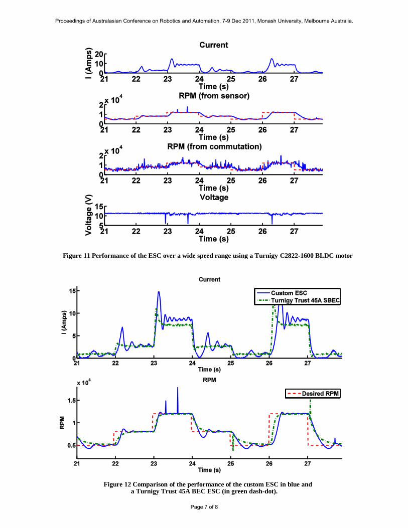
Figure 11 Performance of the ESC over a wide speed range using a Turnigy C2822-1600 BLDC motor
Figure 12 Comparison of the performance of the custom ESC in blue and a Turnigy Trust 45A BEC ESC (in green dash-dot).
Proceedings of Australasian Conference on Robotics and Automation, 7-9 Dec 2011, Monash University, Melbourne Australia.
Page 7 of 8
This same speed test from was performed with a
commercial ESC and the performance of the two ESCs is compared in . The commercial ESC speed response does not overshoot or oscillate and yet reaches the desired val-ue faster. The current also does not oscillate though it does overshoot as expected. The custom ESC current peaks above the desired value and takes longer to stabilise at the desired value compared to the commercial ESC.
6 Conclusions and Future Work
Small robots by design have very limited space for onboard electronics. This poses a problem when many systems, whose functionality is normally provided by separate pieces of hardware, are required to operate the robot. The proposed design solves this by merging the motor control onto the same platform as the higher level systems, using the System-on-Chip design methodology.
On the quadrotor platform the integration of the de-veloped ESC hardware into the same processing platform as the stability controller has the potential to provided im-proved control over motor RPM. Although the imple-mented system works, a possible improvement could be a more sophisticated control algorithm to improve the un-derdamped response. This will improve the performance of the implemented ESC and provide further advantage over commercial off the shelf components.
The next step in this line of work will be to merge the MOSFET motor drive circuitry onto the same PCB as the FPGA. Putting the MOSFET circuitry required for motor drivers on the same board as the computational platform will reduce system size and possible electrical points of failure by reducing the number of connectors required. This is an issue for high mobility robots and will reduce the failure rate of complex systems due to simple compo-nent failures.
Acknowledgements
The authors would like to thank Nathan Gough for his as-sistance with editing and proofreading the paper. The au-thors would also like to thank Nathan Unwin for technical input with respect to the FPGA implementation.
References
[Meyers et al., 2007] J. Meyers, J. Du Plessis, P. Ellis and W. Clark. Design consideration for a low altitude long endurance solar powered unmanned aerial vehicle. AFRICON, pages 1--7, 2007.
[Singh and Singh, 2009] B. Singh and S. Singh. State-of-Art on Permanent Magnet Brushless DC Motor Drives. Journal of Power Electronics, 9(1):1--17, 2009.
[Torres, 2008] D. Torres. Sensorless BLDC Control with Back-EMF Filtering Using a Majority Function. Mi-crchip Corp. Application Note AN1160, 2008.
[Miller, 1989] T. J. E. Miller. Brushless Permanent-Magnet and Reluctance Motor Drives. New York: Ox-ford University Press, 1989.
[Atmel, 2005] Atmel. AVR444: Sensorless control of 3-phase brushless DC motors. 2005.
[Brown, 2002] W. Brown. Brushless DC Motor Control Made Easy. Microchip Corp. Application Note AN857, 2002.
[Gamazo-Real et al., 2010] J. C. Gamazo-Real, E. Vázquez-Sánchez, and J. Gómez-Gil. Position and Speed Control of Brushless DC Motors Using Sensor-less Techniques and Application Trends. Sensors, 10: 6901--6947, 2010.
Proceedings of Australasian Conference on Robotics and Automation, 7-9 Dec 2011, Monash University, Melbourne Australia.
Page 8 of 8


![[03] Chapter02_Logic Design With MOSFETs](https://img.dokumen.tips/doc/110x75/577cd29c1a28ab9e7895a726/03-chapter02logic-design-with-mosfets.jpg)


