Embed Size (px)
Citation preview

Vol.:(0123456789)
SN Applied Sciences (2020) 2:1054 | https://doi.org/10.1007/s42452-020-2869-y
Research Article
Design of an active front‑end rectifier controller with an accurate estimation for the dynamic of its deadbeat current control loop
Ines Ben Ali1 · Mohamed Wissem Naouar1 · Eric Monmasson2
Received: 23 October 2019 / Accepted: 3 May 2020 / Published online: 11 May 2020 © Springer Nature Switzerland AG 2020
AbstractThis paper proposes a control strategy for a grid-connected single-phase Active Front-End (AFE) rectifier that deals with both of ac-side sinusoidal current quality during steady state and dc-bus voltage fluctuations under transient operation issues. This control strategy consists of two control loops. The outer one is used for the control of the dc-bus voltage and is based on a PI controller. The inner loop is used for the control of the grid current and is based on a Deadbeat Predictive (DP) controller that operates with a fixed switching frequency. In order to prevent interactions between the two control loops, the outer control loop dynamic should be at least ten times lower than that of the inner control loop dynamic. For this purpose, a theoretical approach for computing the dynamic of the deadbeat predictive current control is described. Then, the dc-bus voltage controller is designed so that the following constraints are satisfied: (a) the bandwidth of the voltage control loop must be very low with regard to that of the current control loop to prevent interaction between them; (b) the third harmonic component of the grid current resulting from the double line frequency ripples of the measured dc-bus voltage has to be mitigated complying with standards, and (c) reducing the transient fluctuations of the dc-bus voltage caused by instantaneous and high level changes of the active power consumed by the dc load. Simulation and experimental results for the control algorithm validation are also presented and discussed.
Keywords Single-phase AFE rectifier · Dc-bus voltage control · Deadbeat predictive current control
1 Introduction
AC-side current control is still considered one of the most problems in power electronics such as the grid-connected single-phase ac/dc converters. The major concern is how to guarantee a high quality ac-side cur-rent with low harmonic distortion. Predictive control has been widely used in power electronics applications for its simple and intuitive concept to deal with such a prob-lem [1, 2], in particular for current control in single-phase converters [3], inverters [4, 5], and other topologies [6–8]. For this issue, in this work, a predictive current control is applied for a grid-connected single-phase Active
Front-End (AFE) rectifier with a load connected to the dc-bus. The predictive control is characterized by using a system model for predicting the future movements of the controlled variables until a predefined time horizon, and the selection of the optimal actuations according to an optimization criterion [9]. It has been classified into different control techniques as proposed in [10]. Dead-beat Predictive (DP) and continuous control-set Model Predictive Control (MPC) schemes are two well-known techniques in power converters application. The essence of DP and continuous control-set MPC schemes is similar while the kind of implementation is different [3, 11]. In the case of the aforementioned MPC, a cost function is
* Mohamed Wissem Naouar, [email protected]; Ines Ben Ali, [email protected]; Eric Monmasson, [email protected] | 1Université de Tunis El Manar, École Nationale d’Ingénieurs de Tunis, LR11ES15, Laboratoire des Systèmes Électriques, 1002 Tunis, Tunisie. 2SATIE-IUP GEII, Rue d’Eragny, 95031 Cergy Pontoise, France.
Vol:.(1234567890)
Research Article SN Applied Sciences (2020) 2:1054 | https://doi.org/10.1007/s42452-020-2869-y
defined as a criterion and the optimal modulation volt-age vector is selected when the minimization of the cost function is achieved. When the choice of the voltage vec-tor is made in order to make the error equal to zero at the end of the sample period, the predictive controller is often called deadbeat controller. This is the key defini-tion of the DP control.
Regarding the dc-side of the ac/dc converter, a capaci-tive dc-bus is generally used to supply the required dc voltage level and satisfy the dc power demand. In order to properly control the dc-bus voltage, two related major issues have to be dealt with. The first one is related to the transient fluctuations of the dc-bus voltage result-ing from a sudden change in the drawn active power. The second issue is related to the double-line frequency (2ω) ripples in the dc-bus voltage that are inherent in single-phase ac systems [12]. These ripples can affect the control performance since they can cause the addition of a third harmonic component h3 in the grid current during steady state operation. There are different con-trol methods in literature to design the dc-bus voltage controllers [13] for single-phase systems that gener-ally take into consideration only one of the two listed constraints while counseling the other [12, 14]. In this work, the dc-bus voltage is controlled using a standard PI controller that is designed so that the control objec-tives can be achieved. Regarding the inner-current loop, the DP-based control associated with a PWM modulator is applied where the switching frequency is constant. The optimal actuation is obtained here by forcing the predicted current to reach its reference at the end of the sample period (i.e. the controlled variable error is equal to zero) [11, 16]. Moreover, the dynamic of the current control loop is accurately defined in order to prevent interactions with the dc-bus voltage control loop. The ac/dc converter control algorithm has been imple-mented and experimentally validated through a proto-typing platform. The latter consists of a grid-connected single-phase active front-end rectifier where a resistive load is connected in the dc-side. The paper is organ-ized as follows: In Sect. 2 the DP-based current control is described. The section is subdivided into two parts. In the first one, the continuous-time and discreet-time models of the AFE rectifier are given. The second part is reserved for the evaluation of the current control loop dynamic. Section 3 presents the dc-bus voltage control and is subdivided into two subsections. The first one is dedicated to the modeling and analysis of the dc-bus voltage control loop. The second subsection is dedicated to the dc-bus voltage controller design. In Sect. 4 the block diagram of the developed prototyping platform is described and the obtained experimental results are
presented and discussed. Finally, Sects. 5 and 6 draw dis-cussions and conclusions of this work.
2 Model‑based predictive current control
2.1 Deadbeat predictive control (DP) principle
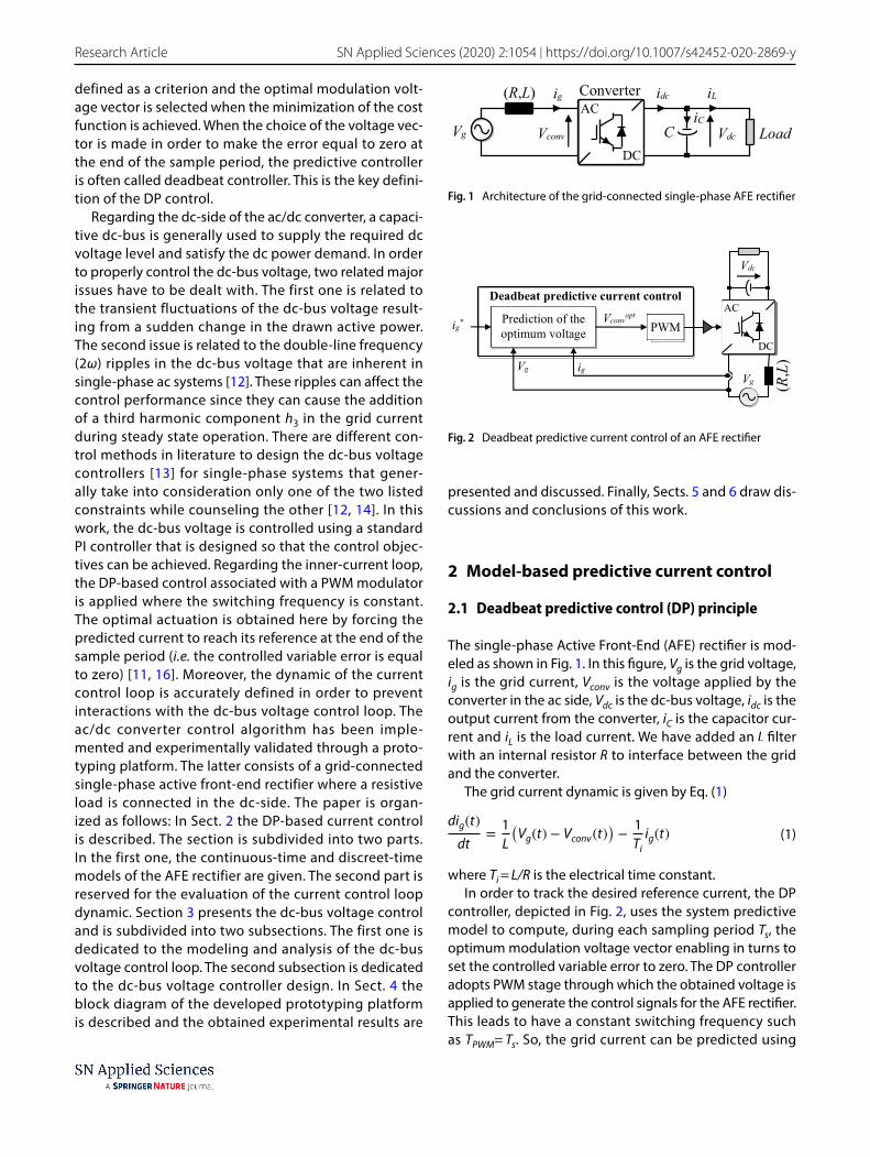
The single-phase Active Front-End (AFE) rectifier is mod-eled as shown in Fig. 1. In this figure, Vg is the grid voltage, ig is the grid current, Vconv is the voltage applied by the converter in the ac side, Vdc is the dc-bus voltage, idc is the output current from the converter, iC is the capacitor cur-rent and iL is the load current. We have added an L filter with an internal resistor R to interface between the grid and the converter.
The grid current dynamic is given by Eq. (1)
where Ti = L/R is the electrical time constant.In order to track the desired reference current, the DP
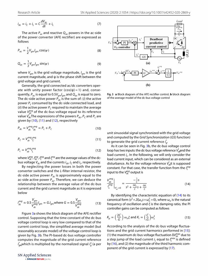
controller, depicted in Fig. 2, uses the system predictive model to compute, during each sampling period Ts, the optimum modulation voltage vector enabling in turns to set the controlled variable error to zero. The DP controller adopts PWM stage through which the obtained voltage is applied to generate the control signals for the AFE rectifier. This leads to have a constant switching frequency such as TPWM= Ts. So, the grid current can be predicted using
(1)dig(t)
dt=
1
L
(Vg(t) − Vconv(t)
)−
1
Tiig(t)
AC
DC
Converter (R,L)
Vg
ig
CiC
idc iL
Vconv Vdc Load
Fig. 1 Architecture of the grid-connected single-phase AFE rectifier
AC
DC
Vconvopt
Vg
Vdc
Prediction of the
optimum voltage
Vg ig
ig*
Deadbeat predictive current control
(R,L
)
PWM
Fig. 2 Deadbeat predictive current control of an AFE rectifier

Vol.:(0123456789)
SN Applied Sciences (2020) 2:1054 | https://doi.org/10.1007/s42452-020-2869-y Research Article
the discrete-time model given by (2), which is obtained by applying to Eq. (1) the forward Euler approximation method
where ig[k + 1] is the predicted current at the (k + 1)th sampling period Ts, and TPWM is the PWM period such as TPWM= Ts.
In order to eliminate the current error at the (k + 1)th sampling period successfully, ig[k + 1] is defined as its refer-ence value ig[k]*
Therefore, by inversing (2) and substituting (3) in (2), we can obtain
where Vconvopt[k] is the optimum average voltage to be applied
by the rectifier so that the grid current reaches its refer-ence value at the end of the kth sampling period.
2.2 Evaluation of the inner control loop dynamic
In order to prevent dynamic interactions between the two AFE rectifier control loops, the bandwidth of the outer dc-bus voltage control loop should be much lower than that of the inner-current control loop (i.e. the outer control loop dynamic must be at least 10 times lower than the inner control loop dynamic). In our case, the time constant τi of the inner-current control loop is unknown. For this reason, we propose in this paragraph a theoretical method to cal-culate the dynamic of the predictive current control. For that, we will consider the worst case corresponding to the lowest current loop dynamic. The considered approach is explained in the following.
Based on (4) and considering a step jump of the load current from 0 (ig[k] = 0) to its maximal value (ig
*[k] = Igmmax),
the optimum voltage to be applied by the power con-verter is calculated by
Since the dc-bus voltage reference Vdc* is equal to 200 V
and supposing that the dc-bus voltage Vdc is accurately controlled, Vconv will vary within ± Vdc
*. Therefore, by substi-tuting the numerical values of parameters (reported in Table 1) in (5), the optimum voltage Vconv
opt to be applied will vary within [− 760 V, + 760 V] boundaries.
(2)
ig[k + 1
]=
(1 −
TPWM
Ti
)ig[k]+
TPWM
L
(Vg[k]− Vconv
[k])
(3)ig[k + 1
]= i∗
g
[k]
(4)Voptconv
[k]=
L
TPWM
[(1 −
TPWM
Ti
)ig[k]− i∗
g
[k]]
+ Vg[k]
(5)Voptconv
[k]= Vg
[k]−
L
TPWM
Imax
gm
To calculate the lowest inner loop dynamic, the low-est value of the voltage Vconv is applied. Then, in the case where Vg[k] = − 170 V, Vconv
opt[k] will be equal to − 760 V which cannot be applied by the converter since the rec-ommended lower boundary of Vconv is equal to − 200 V. Accordingly, Vconv
opt[k] will be set to − 200 V instead of − 760 V. In such a case, the controlled grid current ig will take a time tr
i (greater than the PWM period) to reach its reference value ig
*. According to (5), the time spent by the measured grid current to reach its reference is equal to
By substituting the numerical values of parameters reported in Table 1, we obtain: tr
i= 0.196 ms = 1.96TPWM. This is the largest period that can be taken by the controlled current to reach its reference value. Therefore, if the system is approximated to a first order system the time constant of the current control loop τi will be equal to 49 µs and, consequently, the time constant τV for the dc-bus voltage control loop must be at least 10 times greater than τi. So, to eliminate dynamic interactions between the control loops, the time constant of the dc-bus voltage control loop should be greater than 0.49 ms.
3 DC‑bus voltage control
The purpose of this section is to describe the dc-bus volt-age control loop. For that, this section was divided into two sub-sections; the first one is dedicated to the modeling and analysis of the dc-bus voltage control loop, while the second sub-section is dedicated to the controller design.
3.1 Modeling and analysis of dc‑bus voltage control loop
The dc-bus current idc is equal to
(6)tir=
L
Vg[k]− Vconv
[k] Imax
gm
Table 1 Parameters of the studied system
Parameter Symbol Value Unit
Inductor of the L filter L 10 mHResistor of the L filter R 0.5 ΩCapacitor of the dc-bus C 1100 µFReference value of the dc-bus voltage Vdc
* 200 VPeak value of the grid voltage Vgm √2*120 VMaximal grid current magnitude Igm
max 5.9 AMaximum active power Pmax 500 WPWM period TPWM 100 µs
Vol:.(1234567890)
Research Article SN Applied Sciences (2020) 2:1054 | https://doi.org/10.1007/s42452-020-2869-y
The active Pac and reactive Qac powers in the ac-side of the power converter (AFE rectifier) are expressed as follows
where Vgm is the grid voltage magnitude, Igm is the grid current magnitude, and ψ is the phase shift between the grid voltage and grid current.
Generally, the grid connected ac/dc converters oper-ate with unity power factor (cos(ψ) = 1) and, conse-quently, Pac is equal to 0.5VgmIgm and Qac is equal to zero. The dc-side active power Pdc is the sum of: (i) the active power PL consumed by the dc-side connected load, and (ii) the active power PC required to maintain the average value Vdc
avg of the dc-bus voltage equal to its reference value Vdc
*. The expressions of the powers Pdc, PC and PL are given by (10), (11) and (12), respectively
where Vdcavg, idc
avg, iCavg and iL
avg are the average values of the dc-bus voltage Vdc and the currents idc, iC and iL, respectively.
By neglecting the power losses in both the power converter switches and the L-filter internal resistor, the dc-side active power Pdc is approximately equal to the ac-side active power Pac. Therefore, we can deduce the relationship between the average value of the dc-bus current and the grid current magnitude as it is expressed below
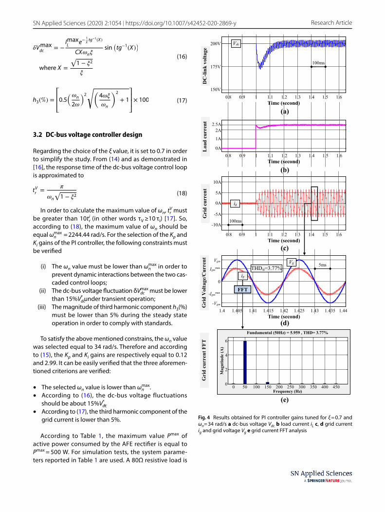
Figure 3a shows the block diagram of the AFE rectifier control. Supposing that the time constant of the dc-bus voltage control loop is very low compared to that of the current control loop, the simplified average model (but reasonably accurate model) of the voltage control loop is given by Fig. 3b. The PI-based dc-bus voltage controller computes the magnitude of the grid current reference Igm*, which is multiplied by the normalized signal ig
n (a per
(7)idc = iC + iL = CdVdc
dt+ iL
(8)Pac =1
2VgmIgm cos(�)
(9)Qac =1
2VgmIgm sin(�)
(10)Pdc = Vavg
dciavg
dc= PL + PC
(11)PC = Vavg
dciavg
C
(12)PL = Vavg
dciavg
L
(13)iavg
dc≈ 0.5
Vgm
Vavg
dc
Igm = G.Igmwhere G = 0.5Vgm
Vavg
dc
unit sinusoidal signal synchronized with the grid voltage and computed by the Grid Synchronization (GS) function) to generate the grid current reference ig
*.As it can be seen in Fig. 3b, the dc-bus voltage control
loop has two inputs: the dc-bus voltage reference Vdc* and the
load current iL. In the following, we will only consider the load current input, which can be considered as an external disturbance. As for the voltage reference Vdc
* it is supposed constant. For that case, the transfer function from the iL
avg input to the Vdc
avg output is
By identifying the characteristic equation of (14) to its canonical form (s2 + 2ξωns + ωn
2 = 0), where ωn is the natural frequency of oscillation and ξ is the damping ratio, the PI controller gains can be computed as follows
According to the analysis of the dc-bus voltage fluctua-tions and the grid current harmonics performed in [15]: (1) the maximum dc-bus voltage fluctuation δVdc
max due to a step jump of the load current iL equal to IL
max is defined by (16), and (2) the magnitude of the third harmonic com-ponent of the grid current is expressed by (17).
(14)Vavg
dc
iavg
L
|||||V∗dc=0
=−
1
Cs
s2 +GKp
Cs +
GKi
C
(15)Kp =(2C
G
)�n� and Ki =
(C
G
)�2
n
DC
AC
Vg
Vdc
Load
Vg ig
ig* Deadbeat
predictive current control
+ -
PI Vdc* Igm
*
(R,L
)
GS ig
n
Vdc controller
(a)
(b)
icavgidc
avg+
- PI
iLavg
1
Cs ΔVdc
GVdc* Vdc
avg+ -
Fig. 3 a Block diagram of the AFE rectifier control, b block diagram of the average model of the dc-bus voltage control
Vol.:(0123456789)
SN Applied Sciences (2020) 2:1054 | https://doi.org/10.1007/s42452-020-2869-y Research Article
3.2 DC‑bus voltage controller design
Regarding the choice of the ξ value, it is set to 0.7 in order to simplify the study. From (14) and as demonstrated in [16], the response time of the dc-bus voltage control loop is approximated to
In order to calculate the maximum value of ωn, trV must
be greater than 10tri (in other words τV ≥10 τi) [17]. So,
according to (18), the maximum value of ωn should be equal ωn
max = 2244.44 rad/s. For the selection of the Kp and Ki gains of the PI controller, the following constraints must be verified
(i) The ωn value must be lower than ωnmax in order to
prevent dynamic interactions between the two cas-caded control loops;
(ii) The dc-bus voltage fluctuation δVdcmax must be lower
than 15%Vdc* under transient operation;
(iii) The magnitude of third harmonic component h3(%) must be lower than 5% during the steady state operation in order to comply with standards.
To satisfy the above mentioned constrains, the ωn value was selected equal to 34 rad/s. Therefore and according to (15), the Kp and Ki gains are respectively equal to 0.12 and 2.99. It can be easily verified that the three aforemen-tioned criterions are verified:
• The selected ωn value is lower than ωnmax.
• According to (16), the dc-bus voltage fluctuations should be about 15%Vdc
*.• According to (17), the third harmonic component of the
grid current is lower than 5%.
According to Table 1, the maximum value Pmax of active power consumed by the AFE rectifier is equal to Pmax = 500 W. For simulation tests, the system parame-ters reported in Table 1 are used. A 80Ω resistive load is
(16)�Vmax
dc= −
ImaxL
e−1
Xtg−1(X )
CX�n�sin
�tg−1(X )
�
where X =
√1 − �2
�
(17)h3(%) =
⎡⎢⎢⎣0.5
��n
2�
�2
��4��
�n
�2
+ 1
⎤⎥⎥⎦× 100
(18)tVr=
�
�n
√1 − �2
0.9 1 1.2 1.1 1.3 1.4 1.5 1.6
DC
-link
vol
tage
200V
175V
150V
Vdc
0.8
100ms
ig
100ms
Gri
d cu
rren
t 0A
5A
10A
-5A
-10A
Time (second)
0.9 1 1.2 1.1 1.3 1.4 1.5 1.60.8
Time (second)
ig
1.4 1.405 1.41 1.415 1.42 1.425 1.43 1.435 1.44
Time (second)
0
0 50 100 150 200 250 300 350 400 4500
2
4
6
Frequency (Hz)
Fundamental (50Hz) = 5.959 , THD= 3.77%
Mag
ntiu
de (A
)
FFT
0.9 1 1.2 1.1 1.3 1.4 1.5 1.60.8
Time (second)
Vg
Igmmax
-Igmmax
Vgm
-VgmGri
d V
olta
ge/C
urre
nt
0A
2.5A
2A
1A
Load
cur
rent
G
rid
curr
ent F
FT
THDig=3.77% 5ms
(a)
(b)
(c)
(d)
(e)
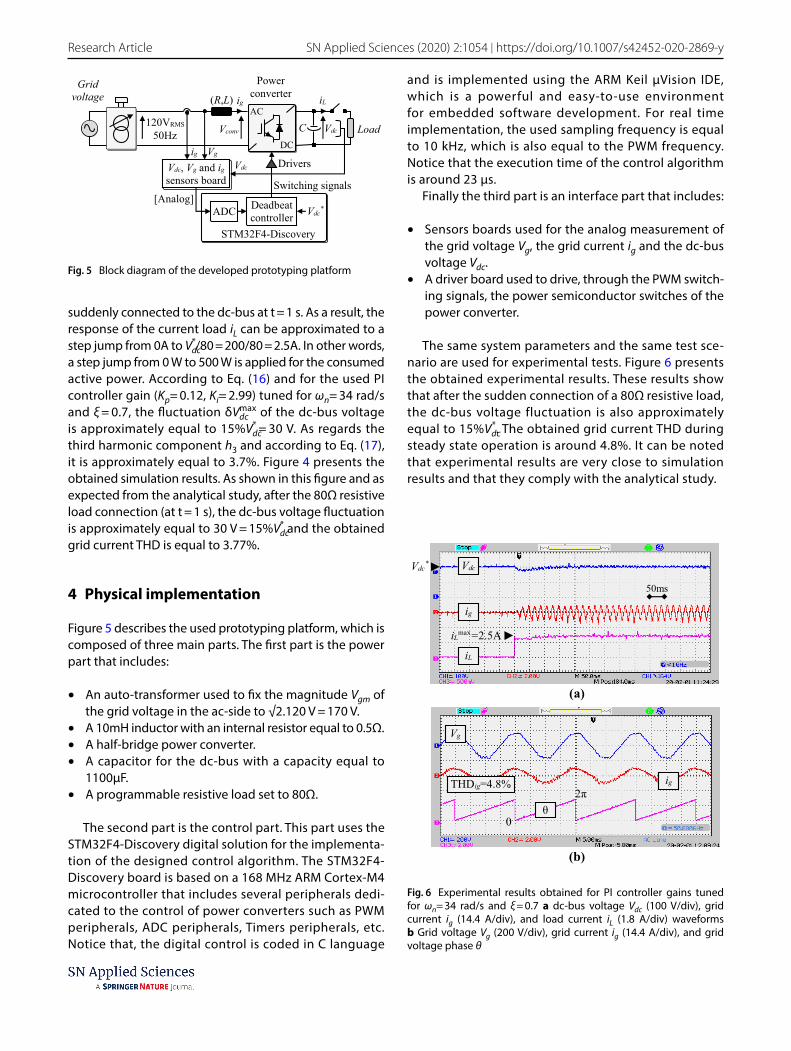
Fig. 4 Results obtained for PI controller gains tuned for ξ = 0.7 and ωn= 34 rad/s a dc-bus voltage Vdc b load current iL c, d grid current ig and grid voltage Vg e grid current FFT analysis
Vol:.(1234567890)
Research Article SN Applied Sciences (2020) 2:1054 | https://doi.org/10.1007/s42452-020-2869-y
suddenly connected to the dc-bus at t = 1 s. As a result, the response of the current load iL can be approximated to a step jump from 0A to Vdc
*/80 = 200/80 = 2.5A. In other words, a step jump from 0 W to 500 W is applied for the consumed active power. According to Eq. (16) and for the used PI controller gain (Kp= 0.12, Ki= 2.99) tuned for ωn= 34 rad/s and ξ = 0.7, the fluctuation δVdc
max of the dc-bus voltage is approximately equal to 15%Vdc
* = 30 V. As regards the third harmonic component h3 and according to Eq. (17), it is approximately equal to 3.7%. Figure 4 presents the obtained simulation results. As shown in this figure and as expected from the analytical study, after the 80Ω resistive load connection (at t = 1 s), the dc-bus voltage fluctuation is approximately equal to 30 V = 15%Vdc
* and the obtained grid current THD is equal to 3.77%.
4 Physical implementation
Figure 5 describes the used prototyping platform, which is composed of three main parts. The first part is the power part that includes:
• An auto-transformer used to fix the magnitude Vgm of the grid voltage in the ac-side to √2.120 V = 170 V.
• A 10mH inductor with an internal resistor equal to 0.5Ω.• A half-bridge power converter.• A capacitor for the dc-bus with a capacity equal to
1100µF.• A programmable resistive load set to 80Ω.
The second part is the control part. This part uses the STM32F4-Discovery digital solution for the implementa-tion of the designed control algorithm. The STM32F4-Discovery board is based on a 168 MHz ARM Cortex-M4 microcontroller that includes several peripherals dedi-cated to the control of power converters such as PWM peripherals, ADC peripherals, Timers peripherals, etc. Notice that, the digital control is coded in C language
and is implemented using the ARM Keil µVision IDE, which is a powerful and easy-to-use environment for embedded software development. For real time implementation, the used sampling frequency is equal to 10 kHz, which is also equal to the PWM frequency. Notice that the execution time of the control algorithm is around 23 µs.
Finally the third part is an interface part that includes:
• Sensors boards used for the analog measurement of the grid voltage Vg, the grid current ig and the dc-bus voltage Vdc.
• A driver board used to drive, through the PWM switch-ing signals, the power semiconductor switches of the power converter.
The same system parameters and the same test sce-nario are used for experimental tests. Figure 6 presents the obtained experimental results. These results show that after the sudden connection of a 80Ω resistive load, the dc-bus voltage fluctuation is also approximately equal to 15%Vdc
*. The obtained grid current THD during steady state operation is around 4.8%. It can be noted that experimental results are very close to simulation results and that they comply with the analytical study.
AC
DC
Power
converter (R,L)
Grid voltage ig
C
iL
Vconv Vdc Load
Deadbeat
controller Vdc
*ADC
STM32F4-Discovery
Drivers
Switching signals
Vdc, Vg and ig
sensors board
Vgig
Vdc
120VRMS
50Hz
[Analog]
Fig. 5 Block diagram of the developed prototyping platform
Vdc* Vdc
ig
iL
iLmax=2.5A
50ms
Vg
igTHDig=4.8%
θ0
2π
(a)
(b)
Fig. 6 Experimental results obtained for PI controller gains tuned for ωn= 34 rad/s and ξ = 0.7 a dc-bus voltage Vdc (100 V/div), grid current ig (14.4 A/div), and load current iL (1.8 A/div) waveforms b Grid voltage Vg (200 V/div), grid current ig (14.4 A/div), and grid voltage phase θ
Vol.:(0123456789)
SN Applied Sciences (2020) 2:1054 | https://doi.org/10.1007/s42452-020-2869-y Research Article
5 Discussion
In the literature, most of the presented dc-bus voltage controllers for single-phase AFE rectifiers consider one or at least two main control objectives. Generally, dc-bus voltage controllers aim to reduce the dc-bus volt-age fluctuations following a sudden load connection (or disconnection) to (or from) the dc-bus. Most of them do not take into account the effect of the double line frequency (2f) ripples of the measured Vdc on the grid current harmonics. The problem of the double line fre-quency ripples is generally treated separately. For exam-ple, some research works have designed controllers that cancelled the Vdc ripples using notch filters tuned at the double line frequency [14, 18–21]. Nonetheless, even if this method efficiently removes these ripples in the measured dc-bus voltage, it leads to a slower transient response; this is due to the introduced delay by the added digital filters. Another solution is to associate PI controller with the feedforward of the dc load (or source) current [22, 23]. This solution enables to efficiently miti-gate the bus voltage fluctuations. However, it presents a major drawback consisting of increasing the dc-/ac-sides coupling of the single-phase grid-connected converters. Other research works achieved the elimination of the double line frequency dc-bus voltage ripples by deriving them to another storage element through an additional active power circuit connected to the dc-bus [12, 24–27]. Although the efficiency of this solution, it will increase the system cost and will reduce its reliability. Compared to the aforementioned related research works, the nov-elty of the proposed AFE controller can be summarized to the following points:
• To prevent interaction between the internal current control loop and the external dc-bus voltage control loop, the lowest dynamic response of the internal con-trol loop is accurately computed and the external one is designed so that its fastest dynamic response remains very low compared to that of the internal control loop.
• The following control objectives are simultaneously considered for the design of the PI-based dc-bus volt-age controller: i) The dynamic of the dc-bus voltage control loop must be very low compared to that of the current control loop; ii) The Vdc-fluctuations, caused by instantaneous and high level changes of the active power, must be minimized and iii) The grid current har-monics mainly caused by the double-line frequency ripples of the measured Vdc must be mitigated.
The obtained simulation and experimental results comply with the analytical study. Also, they confirm the
effectiveness of the designed controller for single-phase AFE rectifiers.
6 Conclusion
This paper presented a control strategy of a grid-con-nected single-phase AFE rectifier connected to a load in the dc-side. A standard PI controller has been used in the outer dc-bus voltage control loop for generating the suit-able magnitude of the active grid current reference. The latter is multiplied by the normalized signal to generate the active grid current reference, which is the input signal of the inner-current control loop. This control loop is based on a deadbeat controller.
The PI controller has been designed while taking into consideration the following constraints: (1) the bandwidth of the outer dc voltage control loop should be much lower than that of the inner-current control loop; (2) the tran-sient fluctuations of the dc-bus voltage must be reduced following a step jump of load current; and (3) the grid current THD must be mitigated during the steady state operation. The effectiveness of the designed controller was illustrated through several simulation and experi-mental results.
Funding This work was supported by the Tunisian Ministry of High Education and Research (TMHER) under Grant LSE-ENIT-LR11ES15 and funded in part by the PHC (Programme Hubert Curien)-Utique program managed by the CMCU (Comité Mixte de Coopération Universitaire).
Compliance with ethical standards
Conflict of interest The authors declare that they have no conflict of interest.
References
1. Kouro S, Cortès P, Vargas R, Ammann U, Rodriguez J (2009) Model predictive control—a simple and powerful method to control power converters. IEEE Trans Ind Electron 56(6):1826–1838
2. Vazquez S, Leon JI, Franquelo LG, Rodriguez J, Young HA, Mar-quez A, Zanchetta P (2014) Model Predictive Control: a review of its applications in power electronics. IEEE Ind Electron Mag 8(1):16–31
3. Song W, Ma J, Zhou L, Feng X (2016) Deadbeat predictive power control of single-phase three-level neutral-point-clamped con-verters using space-vector modulation for electric railway trac-tion. IEEE Trans Power Electron 31:721–732
4. Chan R, Kwak S (2017) Model-based predictive current control method with constant switching frequency for single-phase voltage source inverters. Energies 10:56

Vol:.(1234567890)
Research Article SN Applied Sciences (2020) 2:1054 | https://doi.org/10.1007/s42452-020-2869-y
5. Kwak S, Kim SE, Park JC (2015) Predictive current control meth-ods with reduced current errors and ripples for single-phase voltage source inverters. IEEE Trans Ind Inf 11:1006–1016
6. Vargas R, Ammann U, Hudoffsky B, Rodriguez J, Wheeler P (2010) Predictive torque control of an induction machine fed by a matrix converter with reactive input power control. IEEE Trans Power Electron 25:1426–1438
7. Perez M, Cortes P, Rodriguez J (2008) Predictive control algo-rithm technique for multilevel asymmetric cascaded H-bridge inverters. IEEE Trans Ind Electon 55:4354–4361
8. Xie Y, Ghaemi R, Freudenberg JS (2009) Implicit model predic-tive control of a full bridge DC–DC converter. IEEE Trans Power Electron 24(12):2704–2713
9. Camacho EF, Bordons C (1999) Model predictive control. Springer, NewYork
10. Rodriguez J, Cortes P (2012) Predictive control of power convert-ers and electrical drives, 1st edn. Wiley, New York
11. Liu B, Chen T, Song W (2018) The essential relationship between deadbeat predictive control and continuous- control-set model predictive control for PWM converters. In: The 2018 interna-tional power electronics conference
12. Zhang H, Li X, Ge B, Balog RS (2017) Capacitance, DC voltage utilization, and current stress: comparison of double-line fre-quency ripple power decoupling for single-phase systems”. IEEE Trans Ind Electron Mag 11(3):37–49
13. Alcala J, Barcenas E, Cardenas V (2010) Practical methods for tuning PI controllers in the DC-link voltage loop in back-to-back power converters. In: The 12th IEEE International power elec-tronic congress, pp 46–52, San Luis Potosi, Mexico
14. Levron Y, Canaday S, Erikson RW (2017) Bus voltage control with zero distorsion and high bandwidth for signle-phase solar inverters. IEEE Trans Power Electron. 31(1):258–269
15. Merai M, Naouar MW, Belkhodja IS, Monmasson E (2019) An adaptive PI controller design for DC-link voltage control of sin-gle-phase grid-connected converters. IEEE Trans Ind Electron 66(8):6241–6249
16. Merai M, Naouar MW, Belkhodja IS (2018) An improved DC-link voltage control strategy for grid connected converters. IEEE Trans Power Electron 33(4):3575–3582
17. Merai M, Naouar MW, Slama-Belkhodja I, Monmasson E (2018) Grid connected converters as reactive power ancillary service providers: technical analysis for minimum required DC-link volt-age. Math Comput Simul
18. Hu Y, Zhu ZQ, Odavid M (2017) Instantaneous power control for suppressing the second-harmonic DC-bus voltage under
generic unbalanced operating conditions. IEEE Trans Ind Elec-tron 32(5):3998–4006
19. Balog R, Krein PT (2002) Automatic tuning of coupled induc-tor filters. In: Proceedings of IEEE 33rd annual power electronic specified conference, vol 2, pp 591–596
20. Vongkoom P, Liutanakul P, Wiwatcharagoses N (2018) Analysis and design of DC bus voltage control regarding third harmonic reduction and dynamic improvement of half-bridge microin-verter. In: The 15th international conference on electrical engi-neering/electronics, computer, telecomunacations and informa-tion technology (ECTI-Con)
21. Yazdani A, Iravani R (2010) Voltage-sourced convereters in power systems modeling, control, and applications. Wiley, New York
22. Ch Q, Zhong WL, Ming XC, Krstic M (2012) Reduction of DC-bus voltage ripples and capacitors for single-phase PWM-controlled rectifiers. In: The 38th annual conference on ieee industrial elec-tron. society (IECON)
23. Krein PT, Balog RS, Mirjafari M (2012) Minimum energy and capacitance requirements for single-phase inverters and rectifiers using a ripple port. IEEE Trans Power Electron 27(11):4690–4698
24. Haibing H, Harb S, Kutkut N, Bataresh I, Shen ZJ (2010) Power decoupling techniques for micro-inverters in PV systems-a review. In: IEEE energy conversion congition and exposion (ECCE), pp 620–625
25. Ruxi W, Wang F, Boroyevich D, Burgos R, Rixin L, Puqi N, Rajashek-ara K (2011) A high power density single-phase PWM rectifier with active ripple energy storage. IEEE Trans Power Electron 26(5):1430–1443
26. Li H, Zhang K, Zhao H, Fan S, Xiong J (2013) Active power decou-pling for high-power single-phase PWM rectifiers. IEEE Trans Power Electron 28(3):1308–1319
27. Harb S, Balog RS (2013) Single-phase PWM rectifier with power decoupling ripple-port for double-line-frequency ripple can-cellation. In: IEEE energy conversion congition and exposion (ECCE), pp 1025–1029
Publisher’s Note Springer Nature remains neutral with regard to jurisdictional claims in published maps and institutional affiliations.