Embed Size (px)
Citation preview

Wasswa Charles Sewagudde
Design of a Wireless Gesture Activated PowerPoint Controller
Helsinki Metropolia University of Applied Sciences Bachelor of Engineering Information Technology Bachelor’s Thesis 8 April 2011

2
Author Title Number of pages Date
Wasswa Charles Sewagudde Design of a Wireless Gesture Activated PowerPoint Controller 69 pages + 3 appendices 8 April 2011
Degree Bachelor of Engineering
Degree Programme Information Technology
Specialization Option Embedded Systems Engineering
Supervisor Anssi Ikonen, Senior Lecturer
The desire to give effective presentations lead to the development of different types of visual aids including flip charts, overhead transparencies, posters and digital slide shows. The digital slide shows had improved the effectiveness of the presentation and the audience size, but the need to be next to the keyboard or mouse, created a vacuum for new innovations. There was a need for some form of wireless control of the slides movement. Presenters have always wanted the freedom of movement during their presentation sessions.
The purpose of this project was to design and implement a device that would provide the remote control of PowerPoint slide shows. The project was started by gathering the specification requirements from which design requirements were derived. The selection of the required components was done after thorough examination of dependencies between the different parts of the project. The implementation phase started with the hardware followed by the software. The final phase was testing through which all modules from both the software and hardware were tested before the integration testing was carried out.
The objective of the project was achieved and now it is possible to control the slides remotely using a gesture. The Wireless Gesture activated PowerPoint Controller (WGPC) will give presenters the freedom of movement during their presentations. By imitating book-page opening and closing, with the controller tied on the arm, a presenter is able to move the slides back and forth.
Keywords IIC, I2C, SPI, USB, ISM, gyroscope, accelerometer, Bluetooth, infrared
Abstract

3
Acknowledgements
There are some challenges in life we tend to shy away from, not because we cannot confront them, but because we do not know that we have the strength and what it takes to face them. It is after a good neighbor telling us how talented we are, that we realize that we are better than what we thought we really are. After toppling a number of problems, we acquire experience, skills, competence and a feel that we may not be as weak as we think, after all. I have gone through an experience similar to this, during this project; therefore I must thank those good neighbors who lent a hand before, during and after the project.
I would like to extend my sincere gratitude to all the persons who contributed, in one way or the other, towards the successful completion of this project, especially the staff and students of Metropolia UAS. I cannot mention all of you here due to your big number but allow me point out a few. First and foremost, I would like to thank my supervisor Mr. Ikonen Anssi for his inspiration, encouragement and support during the project. Thank you for trusting me with your project idea. I will always remember these words you said to me when you detected some hesitation in my eyes. “You’re one of the bright students I have taught, you can do this project, am sure. I have the confidence in you, you always produce good results”.
Secondly, I wish to thank Dr. Piironen Antti for listening to me whenever I had troubles with the project, particularly the sensor. Thank you for teaching me to be a good engineer. Thirdly, I wish to extend my thanks to the language adviser, Ms. Taru Sotavalta for helping me correct this document to meet the standards of an academic paper. Last but not the least I would like to thank my fellow students especially Mr. Joseph Hotchkiss and Mr. Lawrence Nwaogo for their constructive arguments which helped me find solutions at the times when my ideas ran dry.
Lastly, I would like to thank my family for their endurance and moral support. I especially wish to thank my sister, Ms. Juliet Namazzi for her encouragement and advice. I felt honored when you said to me, “It is no longer about you, it is about us. You’re our flag bearer. Your failure is our failure.”

4
“The mind, once expanded to the dimensions of larger ideas, never returns to its
original size” (Oliver Wendell Holmes)

5
Contents Abstract ........................................................................................................................................ 2
Acknowledgements ...................................................................................................................... 3
1 Introduction .............................................................................................................................. 8
2 Overview of Interfacing Technologies .................................................................................... 9
2.1 Interfacing in Brief ............................................................................................................ 9
2.2 RS232 (EIA232) ................................................................................................................. 9
2.3 Universal Serial Bus (USB) .............................................................................................. 11
2.3.1 Common USB Terminology ...................................................................................... 11
2.3.2 The Evolution of USB Standards ............................................................................. 12
2.3.3 USB Technologies ..................................................................................................... 12
2.3.4 USB Connectors ........................................................................................................ 13
2.3.5 USB Communication ................................................................................................. 13
2.3.6 USB Device Classes .................................................................................................. 17
2.3. 7 Advantages of USB Interfaces ............................................................................... 18
2.4 Inter-Integrated Circuit (IIC) Bus .................................................................................. 18
2.4.1 Features of IIC Bus .................................................................................................. 19
2.4.2 The IIC Bus Protocol ................................................................................................ 20
2.4.3 IIC Bus Used as an Interface .................................................................................. 20
2.4.4 IIC Bus Data Format ................................................................................................ 21
2.5 Serial Peripheral Interface (SPI) .................................................................................... 21
2.5.1 Data Transmission .................................................................................................... 22
2.5.2 Advantages of SPI .................................................................................................... 23
2.5.3 Disadvantages of SPI ............................................................................................... 24
3 Wireless Technologies ............................................................................................................ 24
3.1 Overview .......................................................................................................................... 24
3.2 Radio Frequency Spectrum ............................................................................................. 25
3.3 Industrial, Scientific and Medical Band (ISM) ............................................................... 26
3.4 Bluetooth .......................................................................................................................... 27
3.4.1 Interfacing PC with Bluetooth ................................................................................. 27
3.4.2 Versions of Bluetooth Specifications ....................................................................... 28
3.5 Infrared ............................................................................................................................ 29

6
4 Sensor Technology ................................................................................................................. 30
4.1 An Overview ..................................................................................................................... 30
4.2 Sensor Terminology ........................................................................................................ 30
4.3 Acceleration sensors........................................................................................................ 32
4.4 Gyroscopes ....................................................................................................................... 34
5 Hardware Design .................................................................................................................... 37
5.1 Overview .......................................................................................................................... 37
5.2 Requirements and Specifications ................................................................................... 37
5.3 Transmitter Design .......................................................................................................... 38
5.3.1 Sensor Selection ....................................................................................................... 38
5.3.2 Radio Frequency Transceiver Chip Selection ......................................................... 40
5.3.3 Microcontroller Selection .......................................................................................... 41
5.3.4 Final Transmitter Design .......................................................................................... 42
5.4 Receiver Design ............................................................................................................... 46
5.4.1 Computer Interface Selection.................................................................................. 47
5.4.2 Microcontroller Selection .......................................................................................... 47
5.4.3 Final Receiver Design ............................................................................................... 48
5.5 Tools and Equipment ...................................................................................................... 50
5.6 Design Challenges ........................................................................................................... 50
6 Software Design ..................................................................................................................... 51
6.1 Overview .......................................................................................................................... 51
6.2 Transmitter Software Design .......................................................................................... 51
6.3 Receiver Software Design ............................................................................................... 53
7 Testing ..................................................................................................................................... 56
7.1 Testing Overview ............................................................................................................. 56
7.2 Transmitter and Receiver Hardware Testing ................................................................ 56
7.3 Transmitter and Receiver Software Testing .................................................................. 58
7.4 Integration Testing .......................................................................................................... 59
7.5 Future Developments ...................................................................................................... 59
9 Conclusion ............................................................................................................................... 61
References .................................................................................................................................. 62

7
Appendixes ................................................................................................................................. 65
Appendix 1: WGPC Sensor Module Schematics and PCB ................................................... 65
Appendix 2: Transmitter C-Program codes.......................................................................... 66
Appendix 3: Receiver C-Program Codes .............................................................................. 69

8
1 Introduction
The desire to give effective presentations has been the driving force for the invention of
visual aids. There are several types of visual aids that have been developed to the effect,
such as: flip charts, overhead transparencies, posters or digital slide shows. The challenge
remained on the ease of use during the presentation session. The digital slide shows had
improved the effectiveness of the presentation and the audience size, but the need to be
next to the keyboard or mouse, created a vacuum for new innovations. There was a need
for some form of wireless control of the slides movement. [1]
The purpose of the project was to design a controller that would change the slides
remotely, without contact to the computer keyboard or mouse. The controller would allow
the presenter to change the slides without being a captive to the keyboard or mouse. The
presenter would have improved contact to his or her audience due to increased freedom
of movement.
The main objective of this paper is to highlight the steps that were used during the design
process and the technologies that were relevant to the project. The scope of the project
was limited to controlling PowerPoint slides remotely, so is this report.

9
2 Overview of Interfacing Technologies
2.1 Interfacing in Brief
Interfacing refers to connecting two or more devices together so that they are able to
exchange information. Scientists and engineers have done a commendable job in finding
the best ways in which devices can communicate with one another, and the choice of
which method to use is dictated by the nature of the application involved. This project
aims to find the best and easiest way to interface a computer with other devices or
peripherals. Some of the popular PC interfacing technologies available are discussed here.
The wired technologies are discussed in sections 2.2, 2.3, 2.4 and 2.5. The wireless
technologies are covered in sections 3.4 and 3.5.
2.2 RS232 (EIA232)
Computers have serial ports which are also known as the RS232 port. Data from the
peripherals is transferred in serial form to the computer or terminal. The drawback for
this interface is the need to convert the serial data back to parallel format before being
used [2]. Actually, data is naturally parallel; it is converted to serial for transmission and
converted back to parallel for “consumption”. The implementation of serial communication
is achieved by the use of Universal Asynchronous Receiver Transmitter (UART). Devices
interfaced via the serial cable are either Data Communication Equipment (DCE) such as
modems, and plotters or they are Data Terminal Equipment (DTE) which is normally the
computer or terminal. [2]
The RS232 is an old standard that defines the voltage levels and other parameters used in
serial communication. RS232 serial ports have two types of connectors: D9 and D25. The
D9 is a 9- pin connector whereas D25 is 25 pins [2]. The UART is crucial in the situation
where data is exchanged between devices and the computer and is the main component
of R232. It takes care of the serial-to-parallel conversion of data from the device to the
computer and parallel-to-serial conversion of the data from the PC to the device. A UART-
10
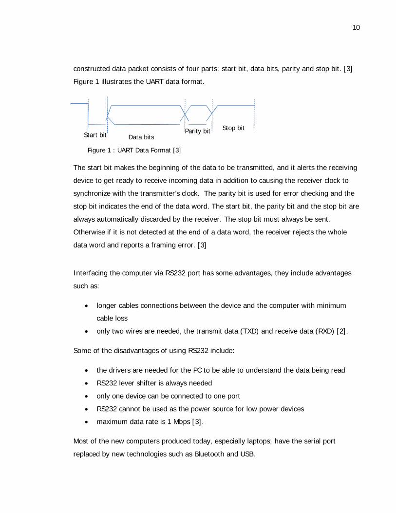
constructed data packet consists of four parts: start bit, data bits, parity and stop bit. [3]
Figure 1 illustrates the UART data format.
The start bit makes the beginning of the data to be transmitted, and it alerts the receiving
device to get ready to receive incoming data in addition to causing the receiver clock to
synchronize with the transmitter’s clock. The parity bit is used for error checking and the
stop bit indicates the end of the data word. The start bit, the parity bit and the stop bit are
always automatically discarded by the receiver. The stop bit must always be sent.
Otherwise if it is not detected at the end of a data word, the receiver rejects the whole
data word and reports a framing error. [3]
Interfacing the computer via RS232 port has some advantages, they include advantages
such as:
longer cables connections between the device and the computer with minimum
cable loss
only two wires are needed, the transmit data (TXD) and receive data (RXD) [2].
Some of the disadvantages of using RS232 include:
the drivers are needed for the PC to be able to understand the data being read
RS232 lever shifter is always needed
only one device can be connected to one port
RS232 cannot be used as the power source for low power devices
maximum data rate is 1 Mbps [3].
Most of the new computers produced today, especially laptops; have the serial port
replaced by new technologies such as Bluetooth and USB.
Start bit Data bits Parity bit Stop bit
Figure 1 : UART Data Format [3]

11
2.3 Universal Serial Bus (USB)
A universal serial bus is a serial bus standard for connecting devices, usually peripheral
devices, to computers. The USB standard is promoted by the USB Implementers Forum
(USB-IF). It is one of the popular means of interfacing with computers due to its
impressive performance and ease of implementation. This has led to many PCs and most
handheld devices to abandon the parallel and serial ports. [4, 5]
2.3.1 Common USB Terminology
The common USB terminologies are illustrated in figure 2. Devices are input/output
peripherals that communicate with a terminal/computer; they can be connected via a Hub
or connected directly to a USB port onto the terminal. A Hub is a device with additional
downstream USB ports whereas a Host is the master that controls the transactions and it
is normally a computer though other devices can also be the Hosts. [6]
There are two kinds of hubs; the bus powered that draws power directly from the host
USB interface, and the self-powered that has an in-built power source [4].The cables that
interconnect the components in a USB network are commonly referred to as USB cables.
There are some input/output devices that also have USB ports; an example is a keyboard.
These types of devices are called Compound Devices, whereas those that implement
two or more different functions are called Composite Devices. [6] Another example of a
compound device is a webcam with an inbuilt microphone.
Teminal /PC Host Hub
Devices
USB Cables
Figure 2: Standard USB Nomenclature [6]

12
2.3.2 The Evolution of USB Standards
There are three version for USB standards; the USB 1.1, USB 2.0 and USB 3.0. The USB
1.1 standard was the first to be developed; it uses a tiered star topology capable of
supporting up 127 devices with a maximum of 6 hubs. It uses a slave/master (host)
relationship with a PC; usually the PC is the master and all other connected devices are
the slaves. The USB 1.1 standard defines two data transfer rates; the Low Speed which is
1.5 Mbps and Full Speed of 12 Mbps. The cable length is limited to a maximum of 5
meters and the devices should not draw more than 500 mA of power. [5]
The USB 2.0 has few modifications from the first version; the additional feature is the high
speed mode with 480 Mbps data transfer rate. All USB 2.0 compatible products must
implement the High Speed mode. The latest version is the USB 3.0 which adds an
additional super speed mode with data transfer rate exceeding 4.8 Mbps. [5] The USB 3.0
standards was developed in response to the high speed demands from new super speed
product developments.
High speed products include flash-based peripherals such as digital cameras and
camcorders, flash memory drives, flash-based digital MP3 and video players, to mention a
few. Another area where high speed is essential is when the interface’s performance
dictates the requirements of the product. Most of the improvements for USB 3.0 from USB
2.0 are done on the Link and protocol layers. [7]
2.3.3 USB Technologies
As more products started incorporating USB ports in their designs, new applications
emerged and lead to new innovations. USB On-The-Go (OTG) and Wireless USB
technologies are the outputs of these innovations. There exists a situation when a device
is required to be a Host at one point and a Device at the other. The OTG is responsible for
this to happen. It provides arbitration mechanism that permits units to negotiate who

13
should be the Host [5]. The wireless USB permits devices to be connected via the radio
interface but still appear to the host as if it was using the ordinary USB cable [4].
2.3.4 USB Connectors
There now many connector types used to interconnect USB units. Originally, there were
two standard types, type A and type B before Mini and Micro were added. Figure 3 show
some of the USB connectors available today.
Figure 3: USB Connector Types (reprinted from Universal serial Bus [8])
Types of USB connectors from left to right are Micro-B plug, Mini-B plug (8-pin), Mini-B
plug (5-pin), Standard-A receptacle, Standard-A plug, Standard-B plug (ruler in
centimeters) [8].
2.3.5 USB Communication
The communication between the host and devices is started by the host. It recognizes the
connected slave devices at boot-up and assigns them each with a unique device-address
to a function. As mentioned in section 2.3.1, a device can have more than one function –
the compound device. Then, all devices send their particulars to the host. These include
their speed, and type of data transfer, among others. This process is known as
Enumeration and the same occurs whenever a USB device is connected to an active host

14
or USB network. The communication between the host and the device function takes place
via a logical channel called a pipe. [4, 5, 8]
On each slave device there exist endpoints. They are unique points in the device which
sources or receives data to or from the host, with a definite address associated with each
one of them. A USB device can have a maximum of 32 endpoints, with 16 endpoints to the
host controller and 16 from the host controller. [4, 8] Figure 4 illustrates the USB pipes
and endpoints with endpoints residing on the device.
Device
The two different categories of logical pipes are the stream and message pipes and they
are dependent on the type of data transfer.
There are four types of data transfer mechanisms:
Control transfer is used by the host to communicate to devices, usually when it
is asking for configuration information or sending commands
Interrupt transfer is used by host to inquire from the input/output devices if
they require immediate attention from the host
Bulk transfer is used for exchanging large quantities of data using all the
remaining available bandwidth left by other forms of data transfer
Logical Pipes
Host Controller
Endpoints in the device
Figure 4: USB pipe and Endpoints [4, 8]

15
Isochronous transfer is used when data transfer is required in real time but with
data loss tolerance. [4, 5, 8]
When the host has enumerated the device and the communication between the host
controller and the devices’ endpoint is established, the device presents its descriptors to
the host. Descriptors are data structures containing the endpoint configurations and
expectations from the host. There are series of descriptors through which the device
expresses itself:
Device Descriptor – a data structure that gives the basic information about the device,
normally the host uses this information to ask for more information and to determine
which device drivers to load. Inside this structure there is another structure, the string
descriptor that gives descriptive text about the device such as device name, manufacturer
and serial number. Configuration Descriptor - a data structure that gives the
functionality and operation of the device, a device can have more than one configuration
and hence multiple configuration descriptors exist. [5, 6, 9]
Interface Descriptor – a data structure that gives the information about the endpoints
supported by the interface, composite devices have as many interface descriptors as there
are device functions. Endpoint descriptors is a data structure that gives the details
about data transfer type, direction of data transfer, packet size, bandwidth requirement,
and polling interval of the endpoint. Endpoint 0 has no descriptor since it is mandatory for
all devices to support it. The contents of all the above mentioned descriptors are given in
Table 1; the order in which the attributes are arranged in practice might not be the same.
[5, 6, 9]

16
Table 1: Contents of typical USB descriptors (compiled from USB Complete [9])
Device Descriptor Configuration Descriptor
Interface Descriptor
Endpoint Descriptor
Length Length Length Length
Descriptor Type Type Descriptor Type Descriptor Type
USB Version No. Total Length This Interface Endpoint Address
Device Class Interfaces Alternate Setting Attributes
Device Protocol This Config No. of Endpoints Max Packet size
Max EP0 Size Config Name Interface Class Polling Interval
Vendor ID Attributes Interface Subclass
Product ID Max Power Interface Protocol
Device Version No. Interface Name
String Descriptor
Manufacturer
Product Name
Serial No.
No. of Configurations
Descriptors shown in table 1 are data structures with data elements given in their
corresponding columns. The string descriptor is part of device descriptor as depicted in
table 1. Some of the data elements of the descriptor are also data structures with data
elements.
17
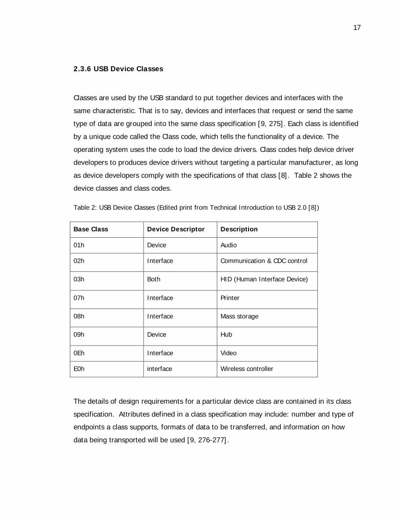
2.3.6 USB Device Classes
Classes are used by the USB standard to put together devices and interfaces with the
same characteristic. That is to say, devices and interfaces that request or send the same
type of data are grouped into the same class specification [9, 275]. Each class is identified
by a unique code called the Class code, which tells the functionality of a device. The
operating system uses the code to load the device drivers. Class codes help device driver
developers to produces device drivers without targeting a particular manufacturer, as long
as device developers comply with the specifications of that class [8]. Table 2 shows the
device classes and class codes.
Table 2: USB Device Classes (Edited print from Technical Introduction to USB 2.0 [8])
Base Class Device Descriptor Description
01h Device Audio
02h Interface Communication & CDC control
03h Both HID (Human Interface Device)
07h Interface Printer
08h Interface Mass storage
09h Device Hub
0Eh Interface Video
E0h interface Wireless controller
The details of design requirements for a particular device class are contained in its class
specification. Attributes defined in a class specification may include: number and type of
endpoints a class supports, formats of data to be transferred, and information on how
data being transported will be used [9, 276-277].

18
2.3. 7 Advantages of USB Interfaces
Some of the features that have attracted embedded systems designers to USB standard
include:
Hot-pluggable: where input/output (I/O) devices can be connected to a computer
while powered on
Ease of use: no need to develop drivers for the I/O devices, devices are
automatically configured
Single connector type: all devices use the same socket type
High performance: up to 480 Mbps data rate for USB 2.0 and 10 times that of USB
3.0
Three speed choices: match the I/O device speed with one of the standard speeds
for optimal design
The interface can support up to 126 devices
Power source for low power devices
Error detection and recovery: data is retransmitted when errors are detected to
ensure reliable data delivery. [6,2]
The popularity of the USB standard is likely to spread rapidly since most of the leaders in
chip manufacturing have joined the bandwagon. This has led to considerable reduction on
the cost of SOC chips enabled with USB controllers. [5]
2.4 Inter-Integrated Circuit (IIC) Bus
The Inter-Integrated Circuit is a bidirectional 2-wire bus, designed by Philips
Semiconductors, for inter-connecting integrated circuits (IC). The IIC bus, also written as
I2C, is not only useful to ICs inter-connections, but it can also be used to facilitate
communication between components linked via a cable. [10]

19
2.4.1 Features of IIC Bus
The IIC bus has features that make it stand out from other interfacing methods for some
application. The characteristics of IIC include:
Two-wire bus; the Serial Data line (SDA) and Serial Clock Line (SCL)
All devices connected to the bus are assigned unique addresses and are accessible
via software using master/slave relationship
Many masters can be accommodated on the same bus in which case collision and
arbitration is employed to prevent data corruption, should more than one master
attempt to initiate data transmission at the same time
Supports up to four serial, 8-bit oriented, bidirectional data transfer modes:
o Standard mode of up to 0.10 Mbps
o Fast-mode of up to 0.40 Mbps
o Fast-mode plus of up to 1 Mbps and
o High-speed mode of up to 3.4 Mbps
On-chip filtering rejects spikes on the bus data line to preserve data integrity
The limiting factor to the number of devices that can be connected on the same bus is
only the maximum bus capacitance. [10] Figure 5 illustrates the connection of master
and slave devices using IIC bus with two pull-up resisters (Rp).
Microcontroller (Master)
IIC Sensor (Slave)
IIC LCD Driver (Slave)
Figure 5: IIC-bus with one master and two slaves [10]
Rp
Vdd
SDA
SCL
Rp

20
The two slaves send their responses to the master, via the SDA line, only when they
detect their address from the data packet sent by the master. The master provides the
clock signal to the responding slave on the SCL line and at the end of the data
transmission, the clock is removed. [11]
2.4.2 The IIC Bus Protocol
The data between devices connected on the bus is carried by the SDA and SCL wires
which are connected to supply voltage with resistors, as illustrated in figure 5. Devices
connected to the bus, each has a unique address that is used to contact it. The inter-
connected devices can be transmitters and receivers or they can also be taken to be
masters or slaves during data transfers. A master is responsible for initiating the
communication and generation of the clock signal on the bus. The clock signal aids the
data exchange between connected devices. [10]
The device to which the data is addressed is called the slave. All other devices to which
data is addressed are considered to be slaves. On the other hand, a transmitter is known
to be the device that sends data to the bus, and the device that receives data from the
bus is the receiver. [10]
2.4.3 IIC Bus Used as an Interface
It is possible to connect embedded systems to a computer using IIC bus. At this point, the
IIC bus is referred to as an interface other than a bus. One of the ways to connect IIC
lines to a computer is by using its parallel port pins, but a bit-banging driver is required for
the implementation of simple IIC master device [11]. The downside of this approach is its
unreliability and risk of damaging the computer with electronic discharge or incorrect
external line connections [11].

21
2.4.4 IIC Bus Data Format
The first byte after a start condition of an IIC data transfer consists of a 7-bit slave
address and a direction bit which differentiates between read and write (R/W). When R/W
is = 0, the master transfers data to the slave, whereas when R/W = 1, the master
receives data from the slave. The data is transferred with most significant bit first (MSB)
as shown in figure 6. The acknowledgement bit (ACK) is sent to the slave after each byte
of the ninth SCL clock. The start and stop conditions are generated by the master. A start
condition is a high-to-low transition on the SDA line while SCL is high whereas a stop
condition is low-to-high while SCL is high. [10]
The IIC standard supports two addressing modes, the 7-bit and the 10-bit. The 7-bit
addressing format is the one illustrated in figure 6. The 10-bit addressing format is
introduced by a leading ‘11110’ after the start condition [11]. It uses the last two address
bits of the first byte plus the 8-bits of the second byte [11].
2.5 Serial Peripheral Interface (SPI)
The serial peripheral interface is a bus and a protocol that was developed by Motorola and
later adopted by other players in industry [12]. It is a 4-wire serial communication
interface used to establish full duplex communication between controllers and peripherals.
[12] The SPI uses Master/Slave mode of communication and the master initiates the data
transfers. The master generates the clock to support the synchronous communication with
the slave or slaves. Like the IIC-bus, multi-master is possible with SPI but rarely
Figure 6: Data transfer on the IIC-bus (Reprinted from I2C interface [11])

22
implemented [12]. The common configuration is one master and many slaves with a
special signal to select individual slaves.
The SPI bus supports up to 10 Mbps data transfer and due to its high speed, it is the
ultimate choice in applications where speed is critical. Some of the areas where SPI is the
dominant interface bus include: converters such as Analog-to-Digital Converters (ADC) and
Digital-to-Digital Converter (DAC), memory modules such as EEPROM and FLASH, sensors
such as temperature, pressure, gyroscopes, acceleration sensors, and USB controllers.
[12]
2.5.1 Data Transmission
To facilitate communication, SPI protocol specifies four logic signals. Two are data lines
and the other two are control lines:
Master Out Slave In (MOSI) – a data signal generated by master and received by
the slave
Master In Slave Out (MISO) – a data signal from the slave and received by the
master
Serial Clock (SCLK) – a control signal generated by the master for synchronizing
data transfers between the master and the slave
Chip Select (CS) or Slave Select (SS)- control signal generated by the master to
choose between the slave devices and it is an active low signal. [12, 13]
Figure 7 illustrates the master/slave relationship in the SPI protocol implementation. As
mentioned in section 2.5, there can be one master and many slaves. Signal lines MOSI,
MISO and SCLK are common to all slaves and CS line is separate for each slave as it is
used to select between them.

23
The master always starts the transaction and supplies the clock to the slave(s). The
master selects the desired slave by setting the CS line to low, waits for some time if
necessary, and then issues the clock pluses. Only the slave whose chip select has been
activated responds but the rest iginores the clock signal, allowing for single slave at a
time. When the session is over, the chip select is set to high state and another one is set
low in a mult-slave communication. Bi-directional communication is supported by the
master reading the MISO line at the same clock cycle as slave reads MOSI line.
2.5.2 Advantages of SPI
The serial peripheral interface has certain benefits that make it a favorite to some
applications. The most significant include:
Support for bi-directional (full duplex) communication
High data rate
Unlimited word length for the bits transferred
Simple hardware interfacing
Lower power consumption compared to IIC
Lack of precision oscillator
One “unique” bus signal per device. [12, 13]
SPI is a popular standard for interfacing the digital sensor and RF modules with
microcontrollers or embedded systems in general.
MOSI
MISO
SCLK
CS’
MOSI
MISO
SCLK
CS’
Figure 7: SPI Master/Slave
SPI Master SPI Slave

24
2.5.3 Disadvantages of SPI
The SPI interface is unsuitable to use for some applications. Some of the downsides of SPI
include:
Requires more pin on IC packages than IIC
No in-band addressing - out-of-band chip select signals are required on shared
busses
No hardware flow control
No slave acknowledgement
Without a formal standard, validating conformance is not possible
Can only be used for short distances unlike RS232 [12, 13]
For most of the application where SPI is favored, the benefits it offers over-shadow its drawbacks. But its lack of formal standard is a really disturbing defect.
3 Wireless Technologies
3.1 Overview
Wireless technology involves the techniques and standards that govern the sending and
receiving of information between devices using air interface. Unlike the interfaces
mentioned in chapter 2 which require physical connection, wireless communication
transmits information by means of electromagnetic waves. The information to be sent is
not always in the form suitable for transmission should be transformed to meet the
characteristic of the transmission channel at the transmitter and then back at the receiver.
The process by which information is translated to a form that meets the requirements of
the transmission channel is called modulation. There are different methods of modulation,
named according to the parameter of the carrier signal they use during the translation.
The carrier signal parameters are: amplitude, frequency and phase and the corresponding
modulation methods are amplitude modulation, frequency modulation and phase

25
modulation respectively. During modulation, the parameter of the carrier signal in
question is made to change with the amplitude of the information signal. The frequency of
the carrier is always much higher than that of the information signal.
Modulation is necessary to be able to conform to regulations governing the use of the
frequency band and bandwidth. All users of wireless or radio communication have a
portion of the frequency band assigned to them and they must work within their
boundaries. An example is an FM radio that broadcasts at 88.8 MHz, has to use frequency
modulation to shift the information signals, at low frequency, to 88.8 MHz frequency. The
receiver demodulates the signal - the reverse of modulation, to recover the original
information.
3.2 Radio Frequency Spectrum
Radio spectrum is the part of the electromagnetic spectrum corresponding to the radio
frequencies. Radio frequencies are frequencies lower than around 300 GHz [15]. The radio
spectrum is divided into parts which are assigned to different radio transmission
technologies and applications. The division is based on the frequency’s wavelength and
suitability for communication application [16]. The frequency band is a section of the
radio spectrum which is set aside, in form of channels or bands, for a particular purpose
as illustrated in figure 8. There are governments and institutions with a task of overseeing
the allocation and use of the radio frequencies. There are regulations in form of standards
to be followed by users to mitigate interference.

26
The illustration in figure 8 also shows the frequency bands right from Very Low Frequency
up to Infra-red and visible light. Moving from left to right, the attenuation of signals by
atmosphere increases and this reduces the distance between the communicating devices
for the information signal to be recovered.
3.3 Industrial, Scientific and Medical Band (ISM)
The ISM bands in the early days were meant to be used for industrial, scientific and
medical purposes but now a common place for communication applications. There are
several communication protocols that have been developed to utilize the advantages
offered by the ISM bands. The fact that ISM bands are reserved internationally and are
exempted from license, makes them attractive to developers of devices that must
universally inter-operate. Some of the protocols utilizing the ISM bands include: Bluetooth,
ZigBee, Wi-Fi and Dash7. The ISM bands are defined by the International
Telecommunication Union Radio communication (ITU-R) but laws governing their use
differ from country to country [16].
The original intended uses of the ISM bands were applications such as Radio Frequency
Identification (RFID) devices, lighting , microwave ovens, low power audio, video and data
links, to mention a few. The communication devices that operate in ISM bands must
tolerate interference from other ISM equipment. For that matter, licensed operations are
Figure 8: The Radio Spectrum (Reprinted from Electromagnetic spectrum [15])

27
discouraged from this band [16]. Some of the other reasons that make ISM band
attractive include: relatively low frequency which makes it appropriate for mobile /
nomadic communications and the global availability, which offers a rare opportunity for
manufacturers to take advantage of the economies of scale that come with operations in a
worldwide market. [16]
3.4 Bluetooth
Bluetooth is a wireless technology which was developed by Ericsson, with intentions of
replacing the cables connecting handheld and or fixed electronic devices [17]. It operates
in 2450 MHz band of the ISM bands. The Bluetooth, like all other wireless technologies
operating in the ISM band, is required to stand radio interference from other devices. To
be able to tolerate interference and fading, Bluetooth deploys radio frequency-hopping
spread spectrum technology [17, 18]. This technology prevents more than on device from
transmitting on the same frequency at the same time. Frequency-hopping is normally
employed when up to eight devices are connected at the same time [18]. The other
technique for minimizing interference is by transmitting low power signals difficult to
intercept by other systems in the same vicinity.
3.4.1 Interfacing PC with Bluetooth
The Bluetooth technology can be used to interface embedded systems with a computer.
Some computers, especially laptops, are embedded with the Bluetooth radio already. The
Bluetooth USB dongle and Bluetooth wireless PC cards are also available to enable device
designers to interface Bluetooth devices with computers [18]. The main focus of the
Bluetooth wireless technology was to address the need for robustness, low power and low
cost [17]. This concept serves well the requirements of handheld devices, which must
consume low power and be cheap at the same time.
Similar to wired interfaces, such as USB, SPI and IIC, Bluetooth devices use a master-
slave relationship to communicate. The master device can interact with up to seven
Bluetooth devices within a network called a piconet. Like USB On-The-Go, Bluetooth
28
master and slave devices can also switch roles. [18] When there are more than two
Bluetooth devices in the network, the master selects the slave to communicate with.
Typically, the master uses small time slots to communicate to all slaves in a round-robin
style [19].
3.4.2 Versions of Bluetooth Specifications
There are mainly three versions of Bluetooth specification in use: the Bluetooth Low
Energy Wireless Technology, the Bluetooth High Speed Technology and the Enhanced
Data Rate [17]. The Bluetooth Low Energy Wireless Technology is the latest
version of all; it was released on 6th July 2010. This version was designed to consume just
a fraction of the power taken by Classic Bluetooth radio, which is good news for small
devices powered on coin-cell batteries. [17] The main benefits of the Bluetooth low energy
wireless technology include:
Ultra-low peak, average and idle mode power consumption
Ability to run for years on standard coin-cell batteries
Low cost
Multi-vendor interoperability
Enhanced range. [17]
The predicted benefactors of this technology are devices such as watches and toys which
can now be easily enhanced with the Bluetooth wireless technology. Other applications
include those that are already enabled with Bluetooth technology in areas such as sports
and fitness, health care, human interface (HIDs) and entertainment devices. [17]
The Bluetooth High Speed Technology offers enhancement to the core specification
to produce a robust powerful wireless connection. This technology capitalizes on features
such as:
Power Optimization
Improved Security
29
Enhanced Power Control
Lower Latency Rates [17]
The Enhanced Data Rate is an advanced short-range wireless technology useful and
easier in connecting Bluetooth devices. The technology makes pairing of the Bluetooth
devices much easy. The benefits of the enhancement to core specification include:
Lower Power Consumption - Reduced power consumption means longer battery
life in devices such as mice and keyboards
Improved Security - For pairing scenarios that require user interaction,
eavesdropper protection makes a simple six-digit passkey stronger than a 16-digit
alphanumeric character random PIN code. The Enhanced Data Rate also offers
"Man-in-the- Middle" protection that in reality eliminates the possibility of an
undetected third party intercepting information.
Near Field Communication - The pairing enhancements provided by the enhanced
data rate enabled the use of near field communication (NFC). [17]
3.5 Infrared
The Infrared (IR), as shown in figure 8, is a light wave below the visible spectrum. The
human eye is unable to see and/ or interpreted infrared light, but can be “felt” in form of
heat [17]. IR is produced from several sources and objects including human bodies, sun
and all hot objects [20]. The fact that infrared can be produced cheaply, and suffers no
interference from electromagnetic waves – a high ranking source of interference
communication systems, are some of the advantages of using IR. The challenge
encountered when using IR is differentiating useful IR from that coming from other
sources. This problem is overcome by employing some type of coding. IR can be
generated in pulses at some frequency and IR receivers are then tuned to detect pluses at
that frequency [20]. This technique is used in many remote controls.
The IR can be used by devices to communicate with a computer having an infrared port
(commonly known as IRDA port) or a USB port. If the computer has only the USB port, a

30
USB-Infrared converter or an infrared add-on to the motherboard would be is required.
The information to be transmitted is coded, by use of amplitude shift keying (ASK) for
example, and then transmitted over IR wave. The receiver decodes the information and
passes it to the computer for interpretation and action taking. The IRDA, mentioned
above, is an acronym for InfraRed Data Association – a transmission standard for two-way
wireless infrared data communication. [20]
The advantage of using IR in communication system is because it is cheap to build into a
device and is fairy reliable. The main drawbacks for IR-based systems are the line of
sight, in which communicating devices have to point at each other to exchange
information which also limits the range, and their support for only “one to one” form of
communication. [17]
4 Sensor Technology
4.1 An Overview
A sensor is a device that converts a physical quantity, such as temperature, into a signal
that can be read by an observer or measured by an instrument. Sensors are of two kinds,
passive and active. Passive sensors do not require some form of external power supply to
give an output signal, whereas active sensors use the external energy source to produce
an output signal. Furthermore, sensors are either digital or analog. Analogue sensors give
a continuous output signal usually proportional to the physical quantity being measured.
On the other hand, digital sensors produce discrete output signal representing a binary
number which can be interpreted by a microprocessor.
4.2 Sensor Terminology
There are a number of terminologies associated with sensors that must be understood
before they can appropriately be applied. The definition of some of the terminologies
might, differ in some way, from sensor to sensor and depending on the quantity being
31
measured, but the big picture is the same. The knowledge about the common sensor
terminologies is useful, since sensor datasheets are always littered with such terms from
which a sensor suitable for an application at hand is identified. The next three paragraphs
explain the commonly encountered terms during sensor selection.
Sensor sensitivity in general terms, gives the minimum input of physical parameter
needed to create a detectable output change. Sensor sensitivity can also be looked at as
the input parameter change required to produce a standardized output change or an
output voltage change for a given change in the input parameter. In many data sheets,
sensitivity error is also given which is none other than the deviation of the measured
results from the expected value. [21]
The range of the sensor gives the maximum and minimum values of the applied
parameter that can be measured [21]. An example is an angular rate sensor with range
of -300 to 300 degrees/second (°/s) and corresponding acceleration range of -6 to +6 g.
It is also possible to have non symmetrical ranges; an example is an LM35 precision
centigrade temperature sensor with the range of -55°C to +150°C. The dynamic range
on the other hand, tells the total range of the sensor from minimum to maximum [20].
The Precision of the sensor gives the level of confidence that the sensor will give the
same correct results if the same quantity is measured a number of times. However, in real
life, the sensor results can hardly be the same on every measurement, the output falls
within a range of values distributed in a behavior relative to the correct value [21].
Resolution of the sensor, on the other hand, tells the smallest detectable incremental
change of input quantity that can be detected in the output signal. The resolution is either
expressed as a proportion of the reading or in absolute terms [21].
The accuracy of the sensor is the ratio of the highest deviation of the value represented
by the sensor to the actual value. The expression for the accuracy can be as a percentage

32
of full scale or in absolute term. Also the offset error of a sensor is the value at the
output of the sensor at a time when there should be zero value. [21]
The linearity of a sensor is determined from its sensitivity over its range. If the
sensitivity is not constant, then the term nonlinearity is used which is the magnitude by
which the output deviate from the actual behavior over the full range of the sensor. The
sensor is said to be linear if the change in the output depends on the change in the
measured quantity. On the other hand, dynamic linearity of a sensor tells the ability of
the sensor to follow rapid changes of the input quantity. Response time of a sensor is
the time required for the sensor output to change from previous state to a final value
within a tolerance band of the correct new value. [21]
4.3 Acceleration sensors
Acceleration sensors (or accelerometers) are electromechanical devices that produce a
voltage proportional to the acceleration of the object on which they are attached. There
are two main types of accelerations to measure using the acceleration sensors: the static
and dynamic acceleration. Static acceleration is related to the earth’s pull on the device,
whereas dynamic acceleration involves the movement and vibration of the device [22].
The mechanism behind which the accelerometer is able to measure the change of speed
lies on the tiny micro-structures, inside the sensor, that are bent by momentum and
gravity [23].
When an object, on which the accelerometer is attached, experience any form of
acceleration, the micro-structures are bent by the same proportion which, in some way, is
translated into a measurable electrical signal. The tiny micro-structures, depending on the
technology employed, is part of a capacitor plates, a resistor or an electrochemical servo.
It is these attachments that are used to measure the extent of the acceleration. [23]
There are a number of ways through which accelerometers are categorized, these include:
their output type, sensing method, manufacturing technology, and other properties. Under

33
output type, there are analog and digital accelerometers. The analog, as the name
suggests, produces a voltage at the output proportional to the type of acceleration, while
digital types have pulse width modulated (PWM) waveform, IIC, or SPI output. On the
other hand, acceleration sensors are classified as capacitive, used for tilt and vibration,
piezoelectric – used for vibration and shock, piezoresistive, used for tilt and vibration, and
electromechanical servo, used for tilt sensing. [22]
Accelerometers find applications in many areas and industries, and are used for activities
such as:
Self-balancing robots
Tilt-mode game controllers
Model airplane auto pilot
Alarm systems
Collision detection
Human motion monitoring
Leveling sensor, inclinometer
Vibration detectors for vibration isolators
G-Force Detectors [23]
The accelerometer is capable of measuring acceleration in three axes; x-axis, y-axis and z-
axis. The sensors are made to be single-axis, double-axis or tri-axis, the choice of which is
dictated by the application. Figure 9 illustrates the three axes that an acceleration sensor
can measure on a robot.
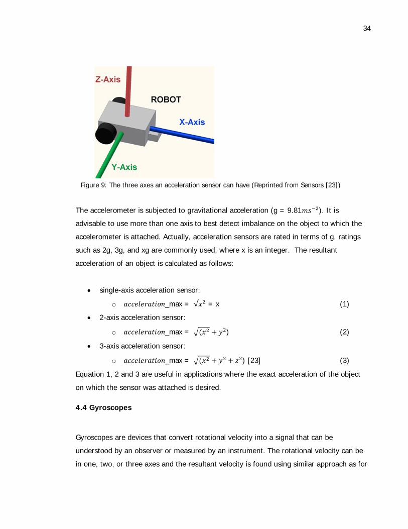
34
The accelerometer is subjected to gravitational acceleration (g = 9.81 ). It is
advisable to use more than one axis to best detect imbalance on the object to which the
accelerometer is attached. Actually, acceleration sensors are rated in terms of g, ratings
such as 2g, 3g, and xg are commonly used, where x is an integer. The resultant
acceleration of an object is calculated as follows:
single-axis acceleration sensor:
o _ max = = x (1)
2-axis acceleration sensor:
o _ max = ) (2)
3-axis acceleration sensor:
o _ max = ) [23] (3)
Equation 1, 2 and 3 are useful in applications where the exact acceleration of the object
on which the sensor was attached is desired.
4.4 Gyroscopes
Gyroscopes are devices that convert rotational velocity into a signal that can be
understood by an observer or measured by an instrument. The rotational velocity can be
in one, two, or three axes and the resultant velocity is found using similar approach as for
Figure 9: The three axes an acceleration sensor can have (Reprinted from Sensors [23])

35
accelerometer seen in section 4.3. The different types of gyroscopes, in some way,
evolved from the traditional mechanical gyroscope which is essentially a spinning wheel or
a disk whose axle is free to take any orientation [23]. The difference between types of
gyroscopes lies on the physical property being exploited to detect the rotational velocity
about some axis. Based on that, three basic types of gyroscopes can be listed, they
include: rotary gyroscopes, vibrating structure gyroscopes and optical gyroscopes [25].
Rotary gyroscopes use the law of conservation of angular momentum to maintain a
constant orientation while spinning. The presence of rotations about a given axis in a
device gives the device the ability to maintain its orientation, and measurement of its
angular velocity is achieved due to the phenomenon of precession [25].
The vibrating structure gyroscopes are Micro-machined Electro-Mechanical System
(MEMS) devices that use Coriolis force [25] to measure the angular velocity of a rotating
object. The gyroscope contains a sensing element composed of a micro-machined mass,
kept in continuous oscillation and capable of reacting, based on the Coriolis principle,
when an angular rate is applied. The angular velocity of the system is detected, in both
magnitude and direction, with the aid of differential capacitance produced by the set of
sensing fingers mounted on different sides inside the sensing element. [25] These types of
gyroscopes are available commercially since they can be produced in small sizes unlike the
rotary type.
The optical gyroscope uses the principle of Sagnac effect to detect mechanical rotation.
To benefit from the Sagnac effect, also known as the Sagnac interference, two beams of
light are made to follow a square or ring trajectory in opposite direction. When the ring is
rotated, one of the beams will travel longer distance than the other and both will not
reach at the same time, hence a phase shift will occur. At the end of the path, the point of
entry, a detector is placed to detect the phase shift between the beams. [24, 25] When
the ring trajectory setup is mounted on to a device, the phase shift detected is in
proportion to the angular velocity of the device. The trajectory is normally made of fiber-

36
optic cable which affects the size of the gyroscope and so is their application. Optical
gyroscopes mostly find applications in naval and aviation where size is a non-issue.
There are some gyroscope specifications which have to match with the application for
which the gyroscope is intended to serve. They include most of those mentioned in section
4.2 and some that are unique to gyroscope include:
number of sensing axes - this give the number and type of axes the gyroscope
can sense
shock survivability - this tell the magnitude of force a gyro can withstand before
failing
bandwidth - is the number of measurement that can be made in a second
angular random walk - is a measure of gyro noise and has units of deg/sec1/2
bias – is the output of the gyro when there is no rotation
bias drift – tells the variation of bias over time
bias instability - It represents the best bias stability that could be achieved for a
given gyro, assuming that bias averaging takes place at the interval defined at the
Allan Variance minimum [25].
Gyroscopes are specified by the number of axes in which rotational acceleration is
measured, such as single, dual, or tri-axis. Three-axis gyroscopes are often implemented
with a three-axis accelerometer to provide a full six degree-of-freedom (DoF) motion
tracking system. [25] The gyroscopes are either analog or digital. The analog gives a
continuous voltages proportional to the angular rate whereas digital give discrete output
as a binary number representation of the angular velocity. Mostly digital gyroscopes use
SPI or IIC interfaces to communication with the outside world. [25]

37
5 Hardware Design
5.1 Overview
The hardware design consists of mainly two parts: the transmitter and receiver designing.
But before the actual designing is started, it is important that a list of the characteristics of
the final product is revisited and translated into requirements which work as the guide
during the hardware components selection. The requirement which establishes the
specifications are identified and are presented in section 5.2.
5.2 Requirements and Specifications
Some of the requirements that were identified from the verbal description of the project
from my supervisor include:
1. the user should be able to control the PowerPoint slides remotely
2. the user should have no physical connection (or contact) with the computer
3. when the user’s arm is twisted (or rotated) to one direction the slide should move
forward and backward when the arm rotates in the opposite direction
4. the component attached to the user’s arm should be small with such a size that it
can be hidden under the sleeve.
It is now clear that wireless communication between the user and the computer is
required and also a motion sensor to detect the movement of the arm is inevitable.
The main components of the WGPC are illustrated in figure 10. The transmitter consists of
a sensor, a microcontroller, an RF transmitter and an antenna. The receiver components
include a USB interface, a microcontroller, an RF receiver and an antenna.

38
The sensor or transducer converts the motion of the human arm into electrical signals; the
signals are filtered and processed by the microcontroller to retrieve the intelligence. The
extracted intelligence, from the signal, is passed on to the RF transmitter for modulation
and transmission. At the receiving end, the receiver’s antenna intercepts the radiated
signal wave; the RF receiver detects/demodulated it and passes it to the microcontroller
for filtering and manipulation. The microcontroller reconditions the signal to a form fit to
control the power point slides. Finally, the signal is sent to its mission, via a USB interface
and the computer’s USB port to the computer or operating system to be particular.
5.3 Transmitter Design
The transmitter consists of all the components on the transmitting side, that is to say, the
sensor, microcontroller and the RF transmitter. The design began with the selection of the
sensor, a microcontroller and radio frequency (RF) transceiver chip. The criteria on which
the choices were made are explained in sections 5.31, 5.3.2 and 5.3.4.
5.3.1 Sensor Selection
The project required a sensor capable of detecting the rate of change of angular
acceleration of the human arm. There were two possible choices of sensors: the
acceleration sensor or a gyroscope. A gyroscope was chosen over acceleration sensor
Sensor
Micro controller
RF
Trans-mitter
RF
Receiver
Micro - controller
USB Interface
PC
Figure 10: The WGPC block diagram
------- Receiver ------------- ------- Transmitter -------------

39
because it required no complex calculation to get the angular rate of change of velocity
from the measured results. Complicated computation would complicate the choice of the
microcontroller. The gyroscope is straight forward; the output is a representation of the
rate of change of angular velocity.
The second task was to choose between analog and digital gyroscope. My choice here was
corrupted by a promise to get some free samples from VTI Technologies by my
supervisor. So I went for digital gyroscope since no other type was present on VTI’s online
store - then. From the project specifications, it was clear that detecting angular rate is in
one direction, this concluded to a single-axis digital output gyroscope. VTI’s SCR1100-D04
single axis gyroscope with digital SPI interface was a good candidate for the job. It has
features such as:
• ±300 º/s angular rate measurement range
• Angular rate measurement around X axis
• Angular rate sensor exceptionally insensitive to mechanical vibrations and shocks
• Superior bias instability for MEMS gyroscopes (<1º/h)
• Digital SPI interfacing
• Enhanced self-diagnostics features
• Small size 8.5 x 18.7 x 4.5 mm (w x l x h)
• Temperature range -40 °C...+125 °C.
The advantages of using a digital gyroscope was that there were no need for an analog-
to-digital converter (ADC) in exchange for more microcontroller pins and time spent
programming SPI to get the results. After spending a number of days interrogating the
gyroscope’s SPI for angular rate in vain, I switched to LPR430AL analog gyroscope from
STMicroelectronics. The analog gyroscope requires an ADC and anti-aliasing filter for
restricting the signal bandwidth so that the sampling theorem is respected. Fortunately, I
needed no designing anti-aliasing filter since it was already integrated in the sensor. The
features of LPR430AL analog gyroscope include:

40
±300 º/s analog gyroscope dual-axis pitch and roll
2.7 V to 3.6 V single-supply operation
Wide operating temperature range (-40 °C to +85 °C)
High stability over temperature
Analog absolute angular-rate outputs
Two separate outputs for each axis (1x and 4x amplified)
Integrated low-pass filters
Low power consumption
Embedded power-down
Embedded self-test
Sleep mode
High shock and vibration survivability.
The switch to the analog gyro was not necessary because it was not possible to extract
any data from the digital type, but I wanted to spend as less time as possible since I was
proving the concept. Actually, it was no critical having accurate results to have the project
working which the digital would give at expense of more programming time.
5.3.2 Radio Frequency Transceiver Chip Selection
The task of selection was more of verification than choosing. For purposes of prototyping,
the CC2500 module, used for school projects, looked sufficient for the job. Though that
was true, there was a need to verify that it had the features needed for this particular
project. From the data sheet, some of the features that were relevant to the task at hand
included:
3.9 V Max Supply voltage
High sensitivity (–104 dBm at 2.4 kBaud, 1% packet error rate)
Low current consumption (13.3 mA in RX, 250 kBaud, input well above sensitivity )
Programmable data rate from 1.2 to 500 kBaud
Frequency range: 2400 – 2483.5 MHz ISM frequency band
OOK, 2-FSK, GFSK, and MSK supported ( On and Off Keying, Frequency Shift
Keying, Gaussian FSK and Minimum Shift Keying)
41
Efficient SPI interface
Programmable channel filter bandwidth
Optional automatic whitening and de-whitening of data.
The points to note here are the supply voltage, the 24 GHz ISM band, modulation
methods, the baud rate, SPI interface, and data whitening and de-whitening. These
features needed to be considered while choosing the microcontroller. Fortunately, most of
them are catered for by the transceiver hardware itself. Something that must be
remembered is the 3V supply and SPI interface. The rest are configured via software.
5.3.3 Microcontroller Selection
The choice of the microcontroller was influenced by the sensor’s requirements and that of
the RF transceiver module. It was clear that the microcontroller had to support SPI
protocol, inbuilt analog to digital converter and had to have at least two ports. For the
prototype I decided to use the Programmable Systems on Chip (PSoC) boards available in
the laboratory. The remaining task was to select the microcontroller series that met the
above requirements. It was found that CY8C29466-24PXI from Cypress Semiconductor
was suitable for the job. Some of the features considered for its suitability included:
3.0V to 5.25V Operating Voltage
Up to 14-Bit ADCs
Programmable Filters and Comparators
Multiple SPI Masters or Slaves
25 mA Sink on all GPIO (General Purpose IO)
Up to 12 Analog Inputs on GPIO
Four 40 mA Analog Outputs on GPIO.
The PSoC board was operated on 5V supply. Yet the sensor and the transceiver use 3
Volts. There should be a way to generate 3 V from 5 Volts. There were two alternatives;
the first one was to redesign the PSoC board to make it operate on 3V, which would take
some time designing and testing. The second was to use some form of voltage translation
and regulation. I took the latter as the transceiver had the translator already designed and
I only needed to design one for the gyroscope.

42
A voltage translator can be a two-way or one-way translator. The two-way translator
allows two devices, operating at different voltage levels, to communicate without knowing
the level differences. It inputs one voltage level and output the other in both directions.
This chip was useful since both the gyroscope and the transceiver have bi-direction
interaction with the microcontroller.
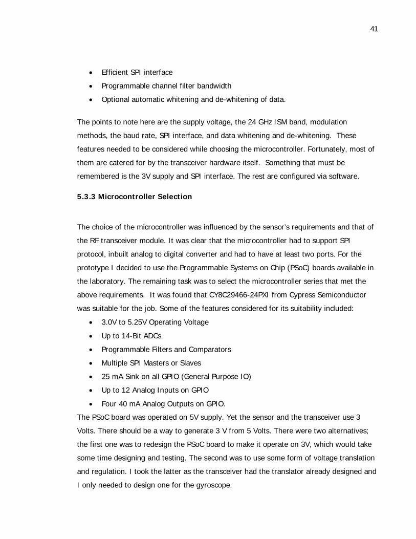
5.3.4 Final Transmitter Design
The on-chip modules, such as ADC and SPI interface, needed to be configured via the
graphical user interface of the microcontroller’s Integrated Development Environment
(IDE). It was the PSoC Designer the starting point for the final design. Some on-chip
modules have special ports to which they can be mounted. For example, the ADC could
only be configured on port0 with its input on pin 1. Figure 11 shows the placement of the
ADC and the SPI modules on chip level design. The analog input was connected to ADC
input through a programmable gain amplifier (PGA) module. The ADC module took two
analog blocks, one for the timer and the other for the counter, and one digital block for
the ADC itself. The outputs and inputs were routed to and from the port pins respectively,
as shown in figure 11.
43
Figure 11: The chip level design for the transmitter
The output of the sensor module is channeled to pin1, since at this point it is known that
the ADC feeds from port0_0. Figure 12 shows the components that make up the sensor
module. The control signals from the microcontroller are level shifted by the voltage
translator before being feed to the gyroscope and the responses from the gyroscope
follows the opposite direction back to the microcontroller. The schematic diagram for the
sensor module is given in appendix 1.
44
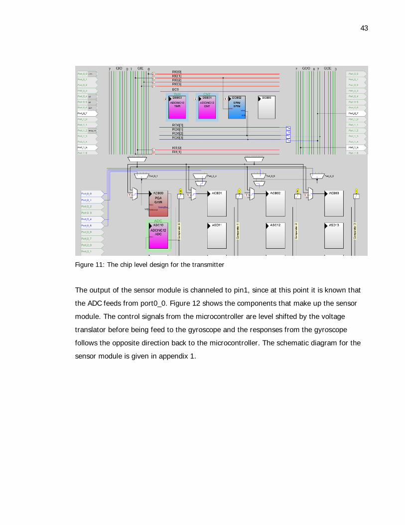
Figure 12: Components of the sensor module
The microcontroller supplies 5 Volts to the module which is converted to 3.3 volts before
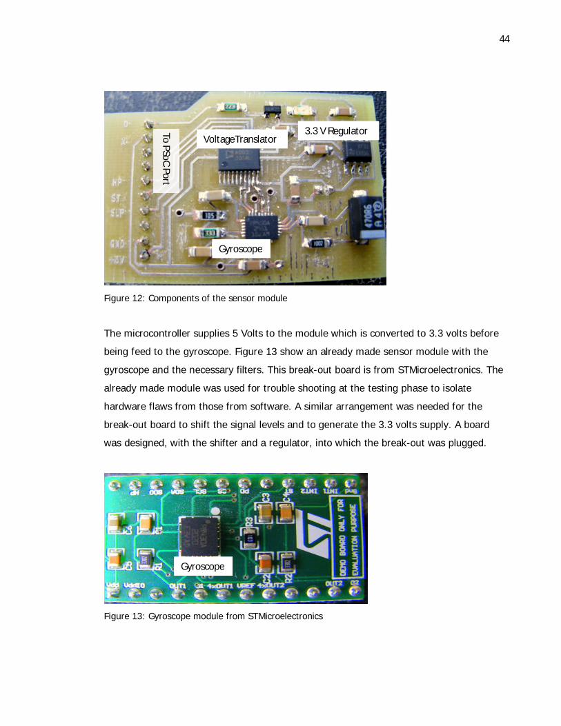
being feed to the gyroscope. Figure 13 show an already made sensor module with the
gyroscope and the necessary filters. This break-out board is from STMicroelectronics. The
already made module was used for trouble shooting at the testing phase to isolate
hardware flaws from those from software. A similar arrangement was needed for the
break-out board to shift the signal levels and to generate the 3.3 volts supply. A board
was designed, with the shifter and a regulator, into which the break-out was plugged.
Figure 13: Gyroscope module from STMicroelectronics
Gyroscope
VoltageTranslator 3.3 V Regulator To PSoC Port
Gyroscope

45
The radio transceiver consists of a voltage regulator, voltage translator and an RF
transceiver module as shown in figure 14. The module was designed to be plugged into a
10-pin port of the PSoC board. Figure 15 shows the complete assembly of the transmitter
with Liquid Crystal Display (LCD) included for debugging purposes during the testing
phase of the project development. The PSoC board has three ports, port_0 to port_2. The
port assignments are: sensor module to port_0, radio transceiver to port_1 and LCD to
port_2. The microcontroller is programmed via the MinProg port indicated in figure 15.
Figure 14: The Radio transceiver module
The radio transceiver module was adapted to the PSOC board via a 10-pin port connector.
The 5 volts power supply from the PSOC board was converted to a 3.3 volts supply using
a 3.3 volts regulator. The voltage translator is a two-way level shifter between 5 volts
from the microcontroller and the 3.3 volts to the RF module.
3.3 V Regulator VoltageTranslator
RF Transceiver Module

46
Figure 15: The complete setup of the transmitter with LCD
The final setup of the transmitter was comprised of the sensor module located onto port0,
radio module onto port1 and LCD onto port2. The PSOC board could be power through a
MinProg port by the programmer or through the 2-pin port by a battery power source.
5.4 Receiver Design
The receiver consists of all the components on the receiving side of the system. Similar to
the transmitter, selecting components to be used in designing the receiver was the first on
the task list. In addition to the components used in the transmitter design, there was an
extra task of identifying the best way the receiver would communicate with the computer.
The transceiver chip chosen for the transmitter qualified to work at the receiving end as
well but the microcontroller did not.

47
5.4.1 Computer Interface Selection
There are at least four methods that can be used to interface an embedded device with a
computer, discussed in sections 2.2, 2.3, 2.4 and 2.5. Interfaces to external devices need
device drivers to aid the interaction between the device and the operating system. Apart
from the USB interface, the rest involved development device drivers – a complex task
that should be avoided if possible. For this reason, the USB interface was chosen. The USB
protocol has the drivers pre-installed on most of the operating systems, as mentioned in
section 2.3. The best way out here was to design the receiver as a human interface
device. The receiver should imitate the keyboard so that every time it is plugged into the
USB port, the computer “thinks” it is a second keyboard.
Now that my controller looked like a keyboard, the next step was to make it behave like a
keyboard. It should be used as if it has the arrow keys, like the keyboard, to be able to
drive the PowerPoint slides back and forth. With the concept conceived, the remaining
part was to choose a microcontroller with inbuilt USB controller, and later on design the
descriptors for the USB keyboard.
5.4.2 Microcontroller Selection
The receiver’s microcontroller, as mentioned in section 5.2, should have an integrated USB
transceiver or USB controller and SPI interface module. The CY8C24894-LFXI
microcontroller from Cypress Semiconductor had the features fit for the job. A voltage
regulator was needed since the USB port supplies 5 Volts and yet the microcontroller and
the transceiver operated on 3.3 Volts. The other alternative was to use the microcontroller
in 5 Volts mode and install a voltage translator to support the communication between the
microcontroller and the transceiver. The dark side of this move was the increased cost of
the controller since the translator costs more than the voltage regulator. For the fact that
the PSOC board with a USB support was selected, using voltage translator was the only
way to go.

48
5.4.3 Final Receiver Design
The physical hardware design began with the chip level design to identify which port and
pins would host what module. The receiver required one SPI and USB module (USB has no
digital block) as show in figure 16. The SPI is for communication between the radio
module and the microcontroller and USB module is for interactions between the computer
and the microcontroller. The radio module was configured to port0 and its control signals
were routed to corresponding pins shown in figure 16.
Figure 16: The chip level design for the receiver
The PSoC board shown in figure 17 has up to five ports, one USB connector, and two
humidity sensor. But only two ports are useful for the project; one for the radio module
and the other for the LCD – used for debugging the software. Figure 18 shows the
complete assembly of the PSoC board used for a receiver.

49
Figure 17: PSoC board with USB interface
The PSOC board with USB interface was designed with several I/O port connectors
allowing support for more than one application. The microcontroller was programmed via
a 5-pin connector.
Figure 18: The complete setup of the receiver with LCD
The RF transceiver module and the LCD were mounted onto a break-out board which was
inserted into the ports of the microcontroller board. The LCD was included to aid software
debugging. The USB connector is located under the board as shown in figure 18.
RF Transceiver Module
USB Connector

50
5.5 Tools and Equipment
The tools that were used during the design included both hardware and software and are
listed against their contribution to the project development.
• The PADS family software were used to support schematic design, layout design
and generation of the LMD files for the milling machine to produce the printed
circuit board (PCB)
• The Digital multi-meter was used during trouble shooting of the hardware, I was
important to know that each section of the circuit had power and it was of the
right level
• The LCD was included t support software debugging, it is a handy tool when
checking for sections of the code that do not execute
• The FilterPro was used for analog filter designing, these includes the anti-aliasing
filters and power supply serge filters
• The Matlab is the tool for digital filter designing but no much digital filtering was
done apart from a running average designed to reduce on the signal noise levels.
5.6 Design Challenges
The main obstacle I faced during the design process was soldering the gyroscope.
Soldering manually a 4x5x1 mm Quad Flat No leads (QFN) packaged chip, was not
“playing with a friend”. I tried several pieces but could not get it right, reason partly being,
wrong tools. Hot air soldering station at Electria saved me from frustration as I could melt
the solder wire with ease. It was by no means easy to find the USB keyboard key-codes;
there are many different key-codes as there are keyboard types.
51
6 Software Design
6.1 Overview
The software part of the project involved two pieces of software; the transmitter software
and the receiver software. The coding was done using the chip manufacturer’s IDE, the
PSoC Designer 5.0. There was interdependence between the hardware designing and
software designing as some features of the hardware had to be implemented or
configured in software. For example, the SPI module, USB module and ADC have to be
configured on chip level first. This meant that some sections of the software had to be
handled before the completion of the hardware design process.
6.2 Transmitter Software Design
The transmitter software controls data acquisition from the sensor, filters off noise to
some level and initializes data lines. The control signals used to create a communication
link between the microcontroller and the RF radio module are generated by the same
transmitter software. Finally, it takes the responsibility of passing data to RF module for
transmission. Some modules employed in the transmitter, as mentioned in section 5.3.4,
are programmable, these include the SPI, LCD, ADC and PGA. The control signals, for the
SPI module, are created using Light Emitting Diodes (LEDs) modules. The control is
achieved through turning ON and OFF of the LEDs. Figure 19 illustrates the program flow
used to produce the C language codes for the transmitter.

52
Figure 19: The Program Flow of the Transmitter software
The flow chart illustrates the main program modules of the transmitter software. When
the program starts, it initializes all the local variables and the digital and analog modules
or blocks before entering the forever loop. While in the loop, data from the ADC’s register
is read and compared to two local constants. If the outcome of the comparison is valid for
the high limit, a forward command is packed and sent for transmission. If it is valid for
the lower limit, a backward command is sent, otherwise an empty command is sent for to
RF radio for transmission if none is valid.

53
The implementation of the flow chart in C language is given in appendix 2. The idea was
to imitate a USB keyboard, the slides movement commands are the real Key codes for
USB keyboard’s arrow keys. For the forward command, 0x4F code is sent and 0x50 code is
sent for the backward command. The command 0x4F is a representation of right arrow
key and 0x50 is the left arrow key.
6.3 Receiver Software Design
The receiver software is responsible for aiding the reception of data by the RF module,
processes it to extract the intelligence, and then coordinate its transfer to the computer.
There are a number of activities handled by the software from the time the receiver is turn
on to the time a slide is controlled remotely. Figure 20 shows the main tasks undertaken
by the receiver software.
When the receiver is powered, variables and modules are initialized. Then, the USB
operation is started and waits to be enumerated by the host computer. When the device is
enumerated, endpoint 1 is loaded to allow data transfers between the device and the host
computer. At the end of the above activities, the program enters a continuous loop from
where data from the transmitter is waited for and read from receiver data-buffer. The data
packet is opened to check its content. The first item to check from the received data is the
address; the packet is dropped if it has a wrong address. The received command is loaded
into the USB transfer buffer, the status of the endpoint is checked, and after receiving an
acknowledgement the data is loaded to endpoint 1.
The implementation of the receiver program flow-chart in C programming language is
show in appendix 3. The hidden detail of the above software design is the implementation
of the report descriptors that was mentioned in chapter 2. Fortunately, there was no need
to write data structures to implement them, as the PSoC designer 5.0 has a USB Setup
Wizard, a graphical user interface (GUI) for designing USB descriptors. However, it is
important to know the right parameters to feed into the wizard, otherwise the device may
fail to be enumerated or work.

54
Figure 20: The Program Flow of the Receiver software
The flow chart illustrates the main program modules of the receiver software. After the
initialization of the variables and hardware modules, the program enters a forever loop
into which tasks such: data reading, data comparison and transmission are done.

55
Figure 21 shows a screen print of the GUI for the USB Setup Wizard with required descriptors clearly shown.
Figure 21: USB setup wizard user interface
It is important to mention the importance of changing the Product ID and Device release
every time the descriptor is edited. When a USB device is plugged into the computer, the
operating system loads its device drivers, after which the OS stores the Product ID and
Device release number. The next time a device is plugged into the computer; the OS

56
compares the current Product ID and Device release number with the ones previously
stored. If they match, the OS retrieves the previously installed drivers. Therefore, the
changes are not recognized when the product ID and device serial number are not
changed.
7 Testing
7.1 Testing Overview Testing is an important stage of product designing as it helps the designer make an
assessment on whether the designed piece of hardware or software works as expected.
The testing involved hardware and software testing for both the transmitter and receiver
as described in the next sections.
7.2 Transmitter and Receiver Hardware Testing
The Voltage presence and voltage levels were the baseline for testing the hardware.
However, some hardware components could not be tested in isolation from the software
as they were configured or implemented in software. Therefore, thorough hardware
testing was done at the integration level, a point where both the hardware and software
were made to interact. The main component that needed testing on the transmitter was
the sensor module. The challenge was that of its dependence on control signals from the
microcontroller. There are three control signals, the High-pass (HP), Self-Test (ST) and
Sleep/Power-down (SLP). The High-pass (HP) signal controls the high-pass filter but it
could be ignored at start.
When the two signals, ST and SLP are at low state (zero or ground), the sensor operates
in normal mode. The ST, SLP and GND pins were connected to ground and VDD to +3.3
Volts - from a DC power supply. Pin X, the output from the sensor, was connected to the
positive probe of a digital multi-meter and of course the other to ground. The digital multi-
meter recorded 1.45 V when the sensor was left stationary. When the sensor was turned
clock-wise, the reading increased by a magnitude proportional to the rate of turning and

57
decreased in a similar manner when it was turned anti-clock-wise. This was a good
indication that the sensor was working properly.
It was necessary to test the ADC too and a test program was written to configure and
display the ADC results on the LCD. When the sensor was rotated, the reading on the LCD
was observed to be changing with magnitudes proportional to rate at which the sensor
was turned. This was also a confirmation that the ADC was converting the sensor voltage
as it was expected. To test the functionality of the RF module, a control receiver was
configured to receive any radio wave transmitted on channel 0 and display its value on
LCD. A test program was written that sent an up-counter value every second. When the
units were powered - the transmitter and receiver, it was observed that the value on the
receiver’s LCD counted up every second – a proof for the proper functioning of the
transmitter.
The receiver had two tests to make: the first one was to test its ability to receive data via
radio link and the second was to test its USB interface. If it could be enumerated, that
would mean that the USB interface was well configured. To start with, a program from the
control receiver was loaded to the receiver with some adjustments to match its
architecture. The same behavior of the counter value, seen earlier on the control receiver,
appeared on the receiver’s LCD.
To test the USB interface, the USB configuration shown in figure 20 was applied to the
receiver. The receiver was then plugged into the USB port of the computer, a message
was seen at the bottom of screen indicating the detection of a USB device. After a few
seconds, a popup message indicated the installation of drivers for the connected USB
device and later, another popup informed about the complete installation of the driver and
readiness to use the hardware. All these messages indicated a successful enumeration of
the receiver. At the end of the tests, it was clear that both the transmitter and receiver
hardware were working as expected.

58
7.3 Transmitter and Receiver Software Testing
Testing the software is intended to uncover software bugs. A software bug refers to a
mistake, failure or fault in the code that makes the computer program to give un-expected
results or behavior. It is important, during testing, to design test cases that cover all
subroutines in the program. All subroutines may not be executed at the same time, but
they should execute at some point if bugs are to be detected.
The subroutines to test were: Initialization(), readData(), and the three decision-making in
the while loop. The easiest way to tell if these routes execute was to place a printing
function inside them, in that, once a routine is executed, some character is printed on the
LCD. Other printing functions were placed in the selection sections and variables were
created which would make the selections true, in sequence. When the program was
loaded to the hardware and the hardware powered, it was observed that characters were
printed on the LCD in their respective places as was expected. The same procedure was
used to test the receiver software; the difference was the absence of the readData
subroutine. The positive results confirmed proper executions of the selection sections and
subroutines, for both the receiver and transmitter software.
The second part was to test the subroutines responsible for sending and receiving data via
radio link. A counter variable, as was in the hardware testing, was created in the
transmitter software, packed into the transmitter buffer and sent. The receiver was
adjusted to print the received data on to the LCD. When the two modules were powered,
an incrementing variable was observed on the receiver’s LCD – a sign of good
transmission and reception of data.
The third test was testing the imitated USB keyboard to control slide shows. Two buttons
were configured on to the receiver; one representing the right arrow key and the second
the left arrow key. The result would be, depending on the button pressed, slides should
move left or right. When the receiver was powered and a button pressed, the slide moved
59
to the right and to the left when the other button was pressed. It was clear that the
receiver had mimicked a USB keyboard as was expected.
7.4 Integration Testing
After testing individual components, it is necessary to check their behavior when they are
connected together to form a system. If the result of this test is agreeable, then it is safe
to say the product is completed. The testing began after editing the transmitter and
receiver software off the test functions and variables. The transmitter and receiver were
assembled to their respective positions, with the receiver’s USB connector plugged into the
computer’s USB port. The transmitter was powered from 6 Volts battery assembly. A
PowerPoint file was open on the computer to which the receiver was attached.
When the transmitter was rotated clockwise and anti-clockwise slowly, the slides did not
move. But when the transmitter was rotated clockwise faster, the slides were seen moving
forward and backward when it was rotated faster anti-clockwise. The rotation was within
180 degrees, and the transmitter was turned from 0o to 180o at a rate similar to that used
to open book pages, fast. After a turn in a desired direction, the arm should be collapsed
slowly in the opposite direction if more slides are required to be opened. The results were
impressing, and the project was complete.
The concept of a wireless gesture-activated PowerPoint controller was proved feasible.
The prototype was designed, implemented, operated and found to be in a complete
working condition.
7.5 Future Developments There is room for improvement on the side of energy saving, cost, and compactness.
There are microcontrollers that consume less energy, are small in size and cheap at the
same time. A microcontroller with an in-built RF module should be used in the project as it
consumes less power and uses less space on the PCB. An example of such a system-on-
chip (SoC) Microcontroller is nRF24LE1 for the transmitter and nRF24LU1 for the receiver

60
both from Nordic Semiconductor. Another alternative could be CC1110Fx for the receiver
and CC430F613x for the transmitter, both from Texas Instrument.
To be able to save power, a transmitter should only transmit when there is data from the
sensor. The idea of sending empty commands wastes energy and should be eliminated in
future designs. The receiver, on the other hand, should go to sleep mode when there is no
data being transmitted. A technique known as Wake-On-Radio (WOR) should be
employed. When WOR is enabled, the controller stays in the low power mode and is
woken up by a radio signal.
It would be good if the receiver had some form of memory where the presenter could
store his or her slides. This would eliminate the possibility of carrying the controller but
forgotten the USB stick hosting the slide shows. An additional feature where the user
adjusts the sensitivity of the controller to the rate of rotation would improve the user
experience. A button is the immediate choice for the implement the sensitivity to the
controller.

61
9 Conclusion
The goal of the project was to design and implement a remote gesture activated
PowerPoint controller. The project involved selection between different wireless
technologies, sensors, interfacing technologies and microcontrollers. Consequently,
gaining knowledge from areas such as interfacing technologies, wireless technologies,
sensor technologies, electronic design, embedded systems programming were
prerequisites to the project success. The choice of most of the components used in the
project was influenced by the desire to use as many already available components as
possible to have the concept proved.
The objective of the project was achieved; the prototype was successfully designed using
the development boards available in laboratories. It is possible to move the slides forward
by rotating the controller clock-wise as if opening book pages, and backward by rotating
the controller anti-clockwise, as if closing book pages. Controlling the slide show by a
simple imitation of opening a book is impressive. The fear, though, remains on the
possibility of the audience to shift the attention from the content of the presentation to
the art employed in giving it.
However, some improvements are necessary to the controller, to make it cheaper, smaller
in size, consume less energy and above all more functional. The microcontrollers should
be configured with wake-on-radio and wake-on-event to be able to save energy. Adding
more functionality can be achieved by including an external flash memory on the receiver
for storage of the slide shows. Addition of buttons onto the transmitter would allow for
adjustable sensitivity.

62
References
1. Presenting Effective Presentations with Visual Aids [online]. Construction Safety and Health Outreach Program, U.S. Department of Labor May 1996, Washington, DC 20210 URL: http://www.osha.gov/doc/outreachtraining/htmlfiles/traintec.html Accessed 21 January 2011
2. Craig Peacock. Interfacing the serial/RS232 Port [online]. Pair Networks. Inc 1995 – 2011 Pittsburgh, USA. URL: http://www.beyondlogic.org/serial/serial.htm. Accessed 21 January 2011
3. Microcontroller UART tutorial [online]. Society of Robots 2010 URL: http://www.societyofrobots.com/microcontroller_uart.shtml
4. Conrad J.M. Introduction to USB Development [online]. College of Engineering UNC, North Carolina USA, 2006 URL: http://www.coe.uncc.edu/~jmconrad/ECGR6185-2006-01/notes/USB.pdf. Accessed 28 January 2011
5. Embedded USB – a brief tutorial [online]. Computer Solutions Ltd 2011, Addlestone, England URL: http://www.computer-solutions.co.uk /info/Embedded_tutorials/ usb_tutorial.htm. Accessed 28 January 2011
6. Hyde John. USB Design by Example, second edition: Intel Press
7. Ravencraft J, Rahman I. USB 3.0 Update, Developers Conference 2007 [Online]. USB Implementers Forum, Beaverton USA URL: http://www.usb.org/developers/wusb/docs/presentations/2007/ Ismail__ Ravencraft _-_USB3.0.pdf. Accessed 31 January 2011
8. A Technical Introduction to USB 2.0 [online]. USB Implementers Forum, Beaverton USA URL: http://www.usb.org/developers/whitepapers/usb_20t.pdf. Accessed 1 February 2011
9. Jan Axelson. USB Complete, second edition. Lakeview Research, 2001 Madison USA
10. I2C-bus specification and user manual Revision 03: NXP Semiconductors 2007, Eindhoven, Netherlands URL: http://www.nxp.com/documents/user_manual/UM10204.pdf. Accessed 6 February 2011
63
11. IIC: I2C Interface [Online]. telos EDV Systementwicklung GmbH 1997, Hamburg Germany. URL: http://www.i2c-bus.org/i2c-bus/. Accessed 9 February 2011
12. SPI Bus Interfaces [Online]. Electronics Engineering Herald , Bangalore India 2006 URL: http://www.eeherald.com/section/design-guide/esmod12.html. Accessed 11 February 2011
13. SPI Interface Specification [Online]. VTI Technologies, Vantaa Finland 2005 URL: http://www.vtitechnologies.jp/documents/data_sheet/ TN15_SPI_Interface_Specification.pdf. Accessed 11 February 2011
14 John Neuhaus. Allocation of Radio Spectrum in the USA [Online]. URL: http://www.jneuhaus.com/fccindex/spectrum.html Accessed 16 February 2011
15 The Electromagnetic Spectrum [Online]. Sky Scan 2005: Alberta, Canada URL: http://www.skyscan.ca/the_electromagnetic_spectrum.htm. Accessed 16 February 2011
16 Industrial Scientific and Medical (ISM) Bands [Online]. Wireless Communication 2006 URL: http://wireless.per.nl/reference/chaptr01/dtmmsyst/ism.htm. Accessed 16 February 2011
17 Bluetooth Special Interest Group. More than just replacing cables [online]. WA2JXE Bluetooth SIG, Inc 2010: Kirkland, Washington USA URL: http://www.bluetooth.com/English/Technology/Works/Pages/default.aspx. Accessed 18 February 2011
18 C. Franklin, J. Layton. How Bluetooth Works [online]. Howstuffworks, 2011 Georgia USA URL: http://www.howstuffworks.com/bluetooth.htm. Accessed 18 February 2011
19 Pav Lucistnik. Bluetooth. FreeBSD Handbook 1995 -2011 URL: http://www.freebsd.org/doc/handbook/network-bluetooth.html. Accessed 20 February 2011
20 Wagner Lipnharski, Infrared Remote Control (Online). UST RESEARCH INC: Orlando, Florida USA URL: http://www.ustr.net/infrared/infrared1.shtml. Accessed 23 February 2011
21 Joseph J. Carr John M. Brown, Sensor Terminology; National Instruments Corporation 2010, Austin, Texas USA URL: http://zone.ni.com/devzone/cda/ph/p/id/227. Accessed 25 February 2011

64
22 Archana Yarlagadda, Accelerometer interface using PSOC. Cypress Semiconductor Corporation, 2009. California, USA URL: http://www.cypress.com/?docID=19786. Accessed 26 February 2011
23 Palmisono, Sensors – Accelerometer. Society of Robots , 2011 URL: http://www.societyofrobots.com/sensors_accelerometer.shtml. Accessed 26 February 2011
24 Marshall Brain. How Gyroscopes Work [online]. Howstuffworks, 2011 Georgia USA URL: http://www.howstuffworks.com/gyroscope.htm. Accessed 4 March 2011
25 Collicuttm. Gyroscope [Online]. SensorWiki.org; Quebec, Canada 2009 URL: http://www.sensorwiki.org/doku.php/sensors/gyroscope#gyroscope. Accessed 4 March 2011

65
Appendixes
Appendix 1: WGPC Sensor Module Schematics and PCB

66
Appendix 2: Transmitter C-Program codes
//-------------------------------------------------------------- //C main for Radio Transmitter, Key codes are radiated // depending on the value read from the Gyroscope //------------------------------------------------------------- #include <m8c.h> // part specific constants and macros #include "PSoCAPI.h" // PSoC API definitions for all User Modules #include "PSoCGPIOInt.h" //PSoC API definitions for I/O interrupts #include "rf.h" // The RF module API #include "stdlib.h" // Add this header to use the ftoa function // Function prototypes void Initialization(void); // Initializes the application void readData(void); // Read the data from Gyro #define RF_CHANNEL 0 // Set radio channel to 0 // Size is defined as Payload + Dest_addr, but... use only payload size #define PACKET_SIZE 7 // Global variables BYTE Tx_packet[PACKET_SIZE] = {0, 0, 0, 0, 0, 0}; // Initialize Transmitter buffer to 0 BYTE RF_channel = 0; // Variable for setting the channel INT iData; // For storing ADC data INT dataBuff[]= {0,0,0,0}; // Moving average filter buffer float dataSum = 0.0; // Average variable BYTE Status_Reg; BYTE rxData[16]; // Start of the main program void main() { Initialization (); // Initialize all modules while (1) // Forever loop { readData(); // Harvest data from the sensor if ( dataSum <= (0-100.0) ) // Check if negative angular acceleration { SleepTimer_SyncWait(512, SleepTimer_WAIT_RELOAD); // delay by a second Tx_packet[0] = 0x00; // Load zeros Tx_packet[1] = 0x00; Tx_packet[2] = 0x50; // Load left arrow key code Tx_packet[3] = 0x00; Tx_packet[4] = 0x00; // Send packet via radio link rf_sendPacket(Tx_packet, PACKET_SIZE); SleepTimer_SyncWait(512, SleepTimer_WAIT_RELOAD); // delay by second dataSum = 0.0; // Reset variable }

67
else if(dataSum > 810) // Check if positive angular acceleration { // delay by 1 second SleepTimer_SyncWait(512, SleepTimer_WAIT_RELOAD); Tx_packet[2] = 0x4f; // Load right arrow key code Tx_packet[3] = 0x00; // Load zeros Tx_packet[4] = 0x00; // Send packet via radio link rf_sendPacket(Tx_packet, PACKET_SIZE); SleepTimer_SyncWait(512, SleepTimer_WAIT_RELOAD); dataSum = 0.0; // Reset variable
}
else // No angular acceleration { Tx_packet[0] = 0x00; // Load zeros Tx_packet[1] = 0x00; Tx_packet[2] = 0x00; Tx_packet[3] = 0x00; Tx_packet[4] = 0x00; // Send packet via radio link rf_sendPacket(Tx_packet, PACKET_SIZE); } } // end of while } // end of main void Initialization(void) { M8C_EnableGInt; // Enable Global Interrupts // Configure 512 Hz SleepTimer SleepTimer_SetInterval(SleepTimer_512_HZ); SleepTimer_EnableInt(); // Enable interrupt SleepTimer_Start(); // start sleep timer //LCD_Start(); // Initialize LCD // Initialize SPIM and the RF module SPIM_Start(SPIM_SPIM_MODE_0 | SPIM_SPIM_MSB_FIRST); SPIM_CS_Start(); // Start SPI master chip select SPIM_CS_On(); // Activate chip select // Initialize Motion Sensor control signals LED_Start(); // Indicator light ST_Start(); // Self-test bit signal ST_Off(); // Set signal low SLP_Start(); // Sleep mode control bit SLP_Off(); // Set signal low //programmable gain amplifier PGA_Start(PGA_MEDPOWER); // ADC initialization ADCINC12_Start(ADCINC12_HIGHPOWER); // Apply power to the SC Block ADCINC12_GetSamples(0); // Have ADC run continuously

68
while(ADCINC12_fIsDataAvailable() == 0); // Loop until value ready ADCINC12_ClearFlag(); // Clear ADC flag iData=ADCINC12_iGetData(); // Get ADC result // The RF module RF_channel = RF_CHANNEL; // Set channel rf_init(); // Initialize radio module rf_setChannel(RF_channel); //Set radio channel } // end of initialization void readData() {
INT dataTemp = 0; int j = 0; While (ADCINC12_fIsDataAvailable() == 0); // Loop until value ready ADCINC12_ClearFlag(); // Clear ADC flag iData = ADCINC12_iGetData(); // Get ADC result // moving average filter while(j < 3) { dataBuff[j] = dataBuff[j+1]; // Shift array backward j++; } dataBuff[3] = iData; // Load current data onto the top of the array j=0; while(j <= 3) { dataTemp += dataBuff[j]; // Add up the contents of the array j++; } dataSum = dataTemp /4; // Compute average } // end of readData
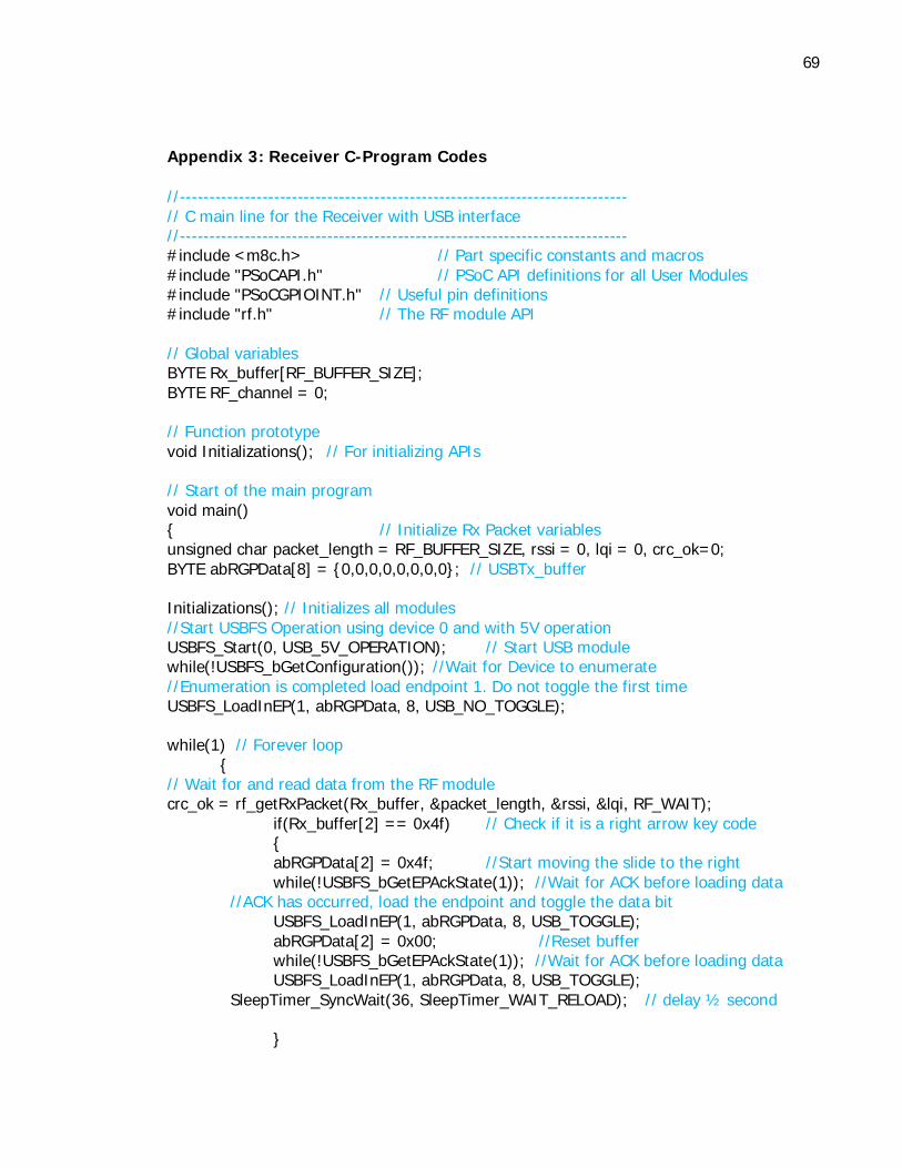
69
Appendix 3: Receiver C-Program Codes //---------------------------------------------------------------------------- // C main line for the Receiver with USB interface //---------------------------------------------------------------------------- #include <m8c.h> // Part specific constants and macros #include "PSoCAPI.h" // PSoC API definitions for all User Modules #include "PSoCGPIOINT.h" // Useful pin definitions #include "rf.h" // The RF module API // Global variables BYTE Rx_buffer[RF_BUFFER_SIZE]; BYTE RF_channel = 0; // Function prototype void Initializations(); // For initializing APIs // Start of the main program void main() { // Initialize Rx Packet variables unsigned char packet_length = RF_BUFFER_SIZE, rssi = 0, lqi = 0, crc_ok=0; BYTE abRGPData[8] = {0,0,0,0,0,0,0,0}; // USBTx_buffer Initializations(); // Initializes all modules //Start USBFS Operation using device 0 and with 5V operation USBFS_Start(0, USB_5V_OPERATION); // Start USB module while(!USBFS_bGetConfiguration()); //Wait for Device to enumerate //Enumeration is completed load endpoint 1. Do not toggle the first time USBFS_LoadInEP(1, abRGPData, 8, USB_NO_TOGGLE); while(1) // Forever loop { // Wait for and read data from the RF module crc_ok = rf_getRxPacket(Rx_buffer, &packet_length, &rssi, &lqi, RF_WAIT); if(Rx_buffer[2] == 0x4f) // Check if it is a right arrow key code { abRGPData[2] = 0x4f; //Start moving the slide to the right while(!USBFS_bGetEPAckState(1)); //Wait for ACK before loading data //ACK has occurred, load the endpoint and toggle the data bit USBFS_LoadInEP(1, abRGPData, 8, USB_TOGGLE); abRGPData[2] = 0x00; //Reset buffer while(!USBFS_bGetEPAckState(1)); //Wait for ACK before loading data USBFS_LoadInEP(1, abRGPData, 8, USB_TOGGLE); SleepTimer_SyncWait(36, SleepTimer_WAIT_RELOAD); // delay ½ second }

70
else if(Rx_buffer[2] == 0x50) // Check if it is a left arrow key code { abRGPData[2] = 0x50; //Start moving Slide backward while(!USBFS_bGetEPAckState(1)); //Wait for ACK before loading data //Load the endpoint and toggle the data bit
USBFS_LoadInEP(1, abRGPData, 8, USB_TOGGLE); abRGPData[2] = 0x00; //Reset buffer while(!USBFS_bGetEPAckState(1)); //Wait for ACK before loading data USBFS_LoadInEP(1, abRGPData, 8, USB_TOGGLE); SleepTimer_SyncWait(36, SleepTimer_WAIT_RELOAD); // delay by ½ second } else // If empty command { abRGPData[2] = 0; // Do nothing to slides while(!USBFS_bGetEPAckState(1)); //Wait for ACK before loading data
//Load the endpoint and toggle the data bit USBFS_LoadInEP(1, abRGPData, 8, USB_TOGGLE);
} } //end of while } //end of main void Initializations() { M8C_EnableGInt; //Enable Global Interrupts SleepTimer_Start(); SleepTimer_SetInterval(SleepTimer_64_HZ); // Set interrupt to a 64 Hz rate SleepTimer_EnableInt(); //LCD_Start(); // Initialize LCD // Initialize SPIM and the RF module itself SPIM_CS_Start(); // SPI master chip select SPIM_CS_On(); // Set chip select SPIM_Start(SPIM_SPIM_MODE_0 | SPIM_SPIM_MSB_FIRST); rf_init(); // Initialize RF module rf_setChannel(RF_channel); // Select RF channel } // end of Initializations