Embed Size (px)
Citation preview

symmetryS S
Article
Design of a New Hybrid Topology of WPT System toAchieve Load-Independent Constant-Current andConstant-Voltage Output
Masood Rehman * , Perumal Nallagownden and Zuhairi Baharudin
Electrical and Electronics Engineering Department, Universiti Teknologi PETRONAS, Seri Iskandar 32610,Perak, Malaysia; [email protected] (P.N.); [email protected] (Z.B.)* Correspondence: [email protected]
Received: 21 June 2020; Accepted: 15 July 2020; Published: 4 September 2020
Abstract: The usage of the Wireless Power Transfer (WPT) technique for charging lithium-ion(Li-ion) batteries of electric vehicles (EVs) is increasing rapidly. The Li-ion battery requires constantcurrent (CC) followed by constant-voltage (CV) supply for efficient battery charging and to enhanceits lifespan. However, it is hard to obtain CC and CV outputs due to the variation of batteryresistance during charging. Moreover, a zero-phase angle (ZPA) of the input source is essential toimprove the power transfer capability. Therefore, this paper proposes a new hybrid compensationtopology to achieve load-independent CC and CV behavior of the WPT system along with ZPA.Two symmetrical coils have been used in the proposed WPT system as transmitter (Tx) and receiver(Rx) coils. A comprehensive mathematical analysis for achieving CC and CV characteristics as well asfor power losses is carried out. A new hybrid compensation is designed by combining Series–Series(SS) and Inductor–Capacitor–Capacitor/Series (LCC-S) compensation topologies along with twoadditional switches. The proposed compensation works on single resonance frequency, and it issimple, reliable, and easy to implement with only one compensation capacitor from the Rx side.Simulations are performed, and a prototype is fabricated to verify the mathematical analysis andsimulation results. The overall result shows that the mathematical analysis and simulations complywith the experimental results. Full load efficiencies of 90.33% and 88.91% are achieved in the CC andCV modes, respectively.
Keywords: wireless power transfer (WPT); symmetrical coils; load independent; constant voltage (CV);constant current (CC); SS topology; LCC-S topology; Zero-Phase Angle (ZPA)
1. Introduction
Wireless Power Transfer (WPT) technology using inductive and magnetic resonant coupling hasbeen broadly investigated because of its variety of applications, such as charging the batteries ofimplantable medical devices, consumer electronic devices, unmanned aerial vehicles (UAVs), electricbicycles (EBs), and electric vehicles (EVs) [1,2]. WPT offers certain benefits in terms of its reliability,environment friendliness, aesthetics, enduring lifespan, and lack of electrical shocks [3,4]. Lithium-ion(Li-ion) batteries are often incorporated for the abovementioned applications. A constant-current (CC)supply followed by constant voltage (CV) irrespective of load fluctuations for charging the battery isoften preferred [5]. It is difficult to achieve CC and CV outputs together in one system with zero-phaseangle (ZPA) switching operation using single-compensation topology. The typical charging behaviorof a Li-ion battery shows that the battery voltage increases drastically during CC charging mode andthen arrives at certain constant levels as illustrated in Figure 1 [6].
Symmetry 2020, 12, 1453; doi:10.3390/sym12091453 www.mdpi.com/journal/symmetry

Symmetry 2020, 12, 1453 2 of 21
Symmetry 2020, 12, x FOR PEER REVIEW 2 of 21
Different methods have been employed to attain load-independent CC and CV outputs, such as frequency tuning, phase shift adjustment, buck or boost converters, and design of a hybrid compensation topology. Load-Independent operation of the WPT system using frequency tuning was proposed in [5]. This method obtained load-independent CC and CV using single-compensation topology at two different frequencies, but a controller was required to automatically supply the desired frequency signal to adjust the frequency. Besides, a proportional integral (PI) controller-based phase shifting method was proposed in [7]. This method is good for achieving load-independent operation; however, it needs an adjustment of the phase by applying pulse width modulation (PWM) to the corresponding four metal oxide semiconductor field effect transistors (MOSFETs) of the power inverter to maintain the required output voltage and current, which increases the losses of the power inverter circuit during the adjustment. However, in that method, zero-phase angle was also not discussed. In addition, the combination of two compensations, including series–series (SS) and parallel-series (PS) along with series-parallel (SP) and parallel-parallel (PP) were suggested in [6] for charging applications; however, in both proposed combinations, two input sources for each combination were required, i.e., constant voltage and constant current. However, it is difficult to provide two input sources for one WPT system. Moreover, when secondary parallel compensation is employed, an additional inductor is required to take the output, which can increase the losses of the WPT system. Multiple compensation topologies were investigated in [8] for CC and CV characteristics, and they noticed that the single topology provides CC or CV behavior but that the CC and CV behavior in one hybrid system was not discussed.
Figure 1. Typical charging profile of a lithium-ion battery.
A method of using a dc-dc converter was proposed in [9] to regulate the output voltage and current. Different frequency and control techniques for voltage and current control were depicted in [5,10,11]; however, these methods did not guaranty frequency stability at single resonance frequency. The analysis of receiver (Rx) side parallel and series compensation topology for load-independent voltage transmission was discussed in [12,13], but the CC output transmission was not considered. A two-sided inductor–capacitor–capacitor (LCC)-compensated topology and its tuning mechanism were illustrated in [14] and offered certain advantages over the SS counterpart in terms of performance; however, the load-independent CV and CC features were not analyzed. Furthermore, it was found in [15] that an LCC compensated network can be efficient for light and heavy loads, especially, in case of heavy loads, the voltage stress on primary compensation capacitors is less in the LCC topology than the SS topology. A tuning method for double-sided inductor-capacitor-inductor (LCL) compensation was proposed in [16], which gives slightly higher efficiency than the traditional tuning method of the LCL network; however, the constant current and voltage features were not presented. Different circuit topologies for EVs were discussed in [17–19]. The research reported in [17] presented LC-LC2 topology, but only load-independent voltage gain was achieved. The authors have utilized SS topology and have calculated the voltage transfer function with varying loads in [20]. They found that the voltage transmission rate can be maximized by minimizing the parasitic
Figure 1. Typical charging profile of a lithium-ion battery.
Different methods have been employed to attain load-independent CC and CV outputs, such asfrequency tuning, phase shift adjustment, buck or boost converters, and design of a hybrid compensationtopology. Load-Independent operation of the WPT system using frequency tuning was proposedin [5]. This method obtained load-independent CC and CV using single-compensation topology attwo different frequencies, but a controller was required to automatically supply the desired frequencysignal to adjust the frequency. Besides, a proportional integral (PI) controller-based phase shiftingmethod was proposed in [7]. This method is good for achieving load-independent operation; however,it needs an adjustment of the phase by applying pulse width modulation (PWM) to the correspondingfour metal oxide semiconductor field effect transistors (MOSFETs) of the power inverter to maintainthe required output voltage and current, which increases the losses of the power inverter circuit duringthe adjustment. However, in that method, zero-phase angle was also not discussed. In addition,the combination of two compensations, including series–series (SS) and parallel-series (PS) along withseries-parallel (SP) and parallel-parallel (PP) were suggested in [6] for charging applications; however,in both proposed combinations, two input sources for each combination were required, i.e., constantvoltage and constant current. However, it is difficult to provide two input sources for one WPT system.Moreover, when secondary parallel compensation is employed, an additional inductor is required totake the output, which can increase the losses of the WPT system. Multiple compensation topologieswere investigated in [8] for CC and CV characteristics, and they noticed that the single topologyprovides CC or CV behavior but that the CC and CV behavior in one hybrid system was not discussed.
A method of using a dc-dc converter was proposed in [9] to regulate the output voltage andcurrent. Different frequency and control techniques for voltage and current control were depictedin [5,10,11]; however, these methods did not guaranty frequency stability at single resonance frequency.The analysis of receiver (Rx) side parallel and series compensation topology for load-independentvoltage transmission was discussed in [12,13], but the CC output transmission was not considered.A two-sided inductor–capacitor–capacitor (LCC)-compensated topology and its tuning mechanismwere illustrated in [14] and offered certain advantages over the SS counterpart in terms of performance;however, the load-independent CV and CC features were not analyzed. Furthermore, it was foundin [15] that an LCC compensated network can be efficient for light and heavy loads, especially, in caseof heavy loads, the voltage stress on primary compensation capacitors is less in the LCC topology thanthe SS topology. A tuning method for double-sided inductor-capacitor-inductor (LCL) compensationwas proposed in [16], which gives slightly higher efficiency than the traditional tuning method ofthe LCL network; however, the constant current and voltage features were not presented. Differentcircuit topologies for EVs were discussed in [17–19]. The research reported in [17] presented LC-LC2topology, but only load-independent voltage gain was achieved. The authors have utilized SS topologyand have calculated the voltage transfer function with varying loads in [20]. They found that thevoltage transmission rate can be maximized by minimizing the parasitic resistance of primary andsecondary coils. The switchable hybrid topologies for battery charging of electric vehicles (EVs) and

Symmetry 2020, 12, 1453 3 of 21
electric bicycles (EBs) were presented in [21–24], but the switches were employed in the receiver (Rx)side rather than the transmitter side (Tx). The switching from the Rx side is not preferred because asingle transmitter can be used for charging many receivers; therefore, it is strenuous to implement aswitchable compensation network for every receiver.
This article emphasizes the design of a new hybrid compensation network to satisfy the needs ofthe battery charging mechanism. Symmetrical coils have been utilized as Tx and Rx coils to implementthe hybrid topology of a WPT system. A comprehensive theoretical analysis is carried out to designthe parameters for obtaining the CC and CV modes of operations. The proposed hybrid topologyutilizes two different compensations including SS and LCC-S along with two additional switches.The systematic design equations are derived for both the topologies to ensure the load-independentCC or CV output. To diminish the voltage–current rating and to increase the efficiency of the inverter,the equations of input impedance are derived to attain the zero-phase angle (ZPA). The switchesare employed from the primary side rather than the secondary side to minimize the Rx circuit size;therefore, the control mechanism and its parameters can be significantly simplified. The proposedtopology operates at single resonant frequency, which is independent of the coupling factor and loadsettings, this adds an extra benefit to the proposed design. The design equations of the proposedtopology can be used for any type of power requirement.
This article is arranged as follows: Section 2 comprises the modeling of the CC and CV modeoperation of a WPT system. Section 3 consists of the implementation of proposed topology and coilstructure design. Power loss analysis is presented in Section 4. Section 5 presents the simulation andanalysis of proposed topology. Experimental results are provided in Section 6. The voltage, current,and power gain analysis is discussed in Section 7. Finally, the conclusion is presented in Section 8.
2. Mathematical Modeling of Proposed Topology
A hybrid topology is proposed in this research, which includes SS and LCC-S compensationto obtain CC and CV characteristics. Mathematical modeling is accomplished for both topologies,separately. Thereafter, the parameters of hybrid topology are obtained by combining both compensationsalong with two additional switches.
2.1. System Modeling of SS Topology
A complete circuit design of the WPT system using SS compensation is depicted in Figure 2a andits equivalent circuit is illustrated in Figure 2b. The following equations can be extracted with the helpof Kirchhoff’s Voltage Law (KVL).
US = Z1IS − jωM12IL (1)
0 = −jωM12IS + Z2IL (2)
where Z1 = 1jωC1
+R1 + jωL1 and Z2 = jωL2 +R2 +1
jωC2+RL. where US is the voltage of the source,
which is applied on the Tx side at resonance frequencyω. Besides, Z1 and Z2 are the impedances of theTx and Rx sides, respectively. The mutual inductance M12 between the primary and secondary sidescan be formulated with reference to coupling coefficient k and coil self-inductances and is as follows:
M12 = k√
L1 L2 (3)
It is worth mentioning that the greater value of the coupling coefficient reflects the short airgapbetween the Tx and Rx coil and vice versa. When both the source and load sides work on the resonancefrequency, the currents flowing through the source side and the load side are determined by solvingEquations (1) and (2), which yields the following:
IS =US RL
(ωM12)2 (4)
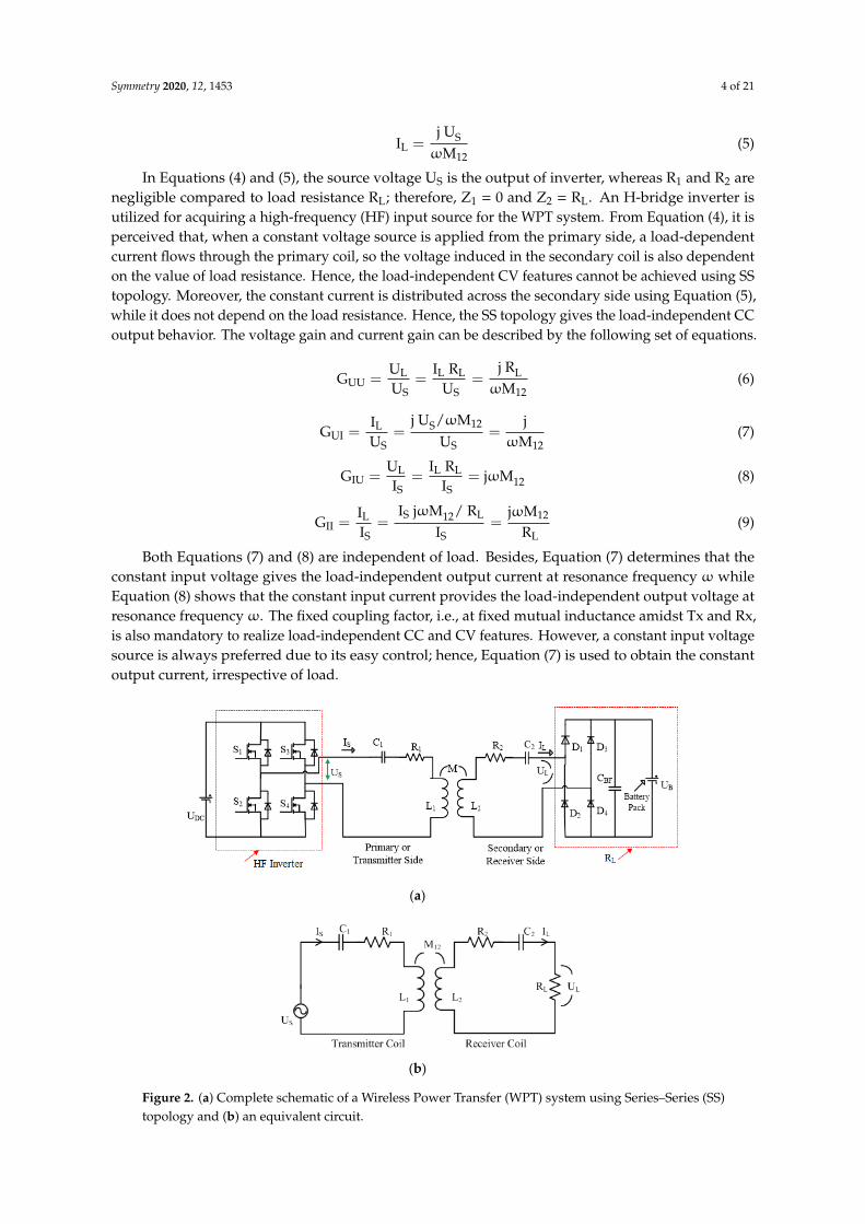
Symmetry 2020, 12, 1453 4 of 21
IL =j US
ωM12(5)
In Equations (4) and (5), the source voltage US is the output of inverter, whereas R1 and R2 arenegligible compared to load resistance RL; therefore, Z1 = 0 and Z2 = RL. An H-bridge inverter isutilized for acquiring a high-frequency (HF) input source for the WPT system. From Equation (4), it isperceived that, when a constant voltage source is applied from the primary side, a load-dependentcurrent flows through the primary coil, so the voltage induced in the secondary coil is also dependenton the value of load resistance. Hence, the load-independent CV features cannot be achieved using SStopology. Moreover, the constant current is distributed across the secondary side using Equation (5),while it does not depend on the load resistance. Hence, the SS topology gives the load-independent CCoutput behavior. The voltage gain and current gain can be described by the following set of equations.
GUU =UL
US=
IL RL
US=
j RL
ωM12(6)
GUI =IL
US=
j US/ωM12
US=
jωM12
(7)
GIU =UL
IS=
IL RL
IS= jωM12 (8)
GII =IL
IS=
IS jωM12/ RL
IS=
jωM12
RL(9)
Both Equations (7) and (8) are independent of load. Besides, Equation (7) determines that theconstant input voltage gives the load-independent output current at resonance frequency ω whileEquation (8) shows that the constant input current provides the load-independent output voltage atresonance frequencyω. The fixed coupling factor, i.e., at fixed mutual inductance amidst Tx and Rx,is also mandatory to realize load-independent CC and CV features. However, a constant input voltagesource is always preferred due to its easy control; hence, Equation (7) is used to obtain the constantoutput current, irrespective of load.
Symmetry 2020, 12, x FOR PEER REVIEW 4 of 21
(a)
(b)
Figure 2. (a) Complete schematic of a Wireless Power Transfer (WPT) system using Series–Series (SS) topology and (b) an equivalent circuit.
It is worth mentioning that the greater value of the coupling coefficient reflects the short airgap between the Tx and Rx coil and vice versa. When both the source and load sides work on the resonance frequency, the currents flowing through the source side and the load side are determined by solving Equations (1) and (2), which yields the following:
I = U R(ωM ) (4)
I = j UωM (5)
In Equations (4) and (5), the source voltage US is the output of inverter, whereas R1 and R2 are negligible compared to load resistance RL; therefore, Z1 = 0 and Z2 = RL. An H-bridge inverter is utilized for acquiring a high-frequency (HF) input source for the WPT system. From Equation (4), it is perceived that, when a constant voltage source is applied from the primary side, a load-dependent current flows through the primary coil, so the voltage induced in the secondary coil is also dependent on the value of load resistance. Hence, the load-independent CV features cannot be achieved using SS topology. Moreover, the constant current is distributed across the secondary side using Equation (5), while it does not depend on the load resistance. Hence, the SS topology gives the load-independent CC output behavior. The voltage gain and current gain can be described by the following set of equations.
G = U U = I R U = j RωM (6)
G = I U = j U /ωM U = jωM (7)
G = U I = I R I = jωM (8)
Figure 2. (a) Complete schematic of a Wireless Power Transfer (WPT) system using Series–Series (SS)topology and (b) an equivalent circuit.

Symmetry 2020, 12, 1453 5 of 21
Furthermore, the SS topology or any other topology can provide the zero imaginary reflectedimpedance if both the primary and secondary coils are in resonance. Here, also the primary andsecondary sides are adjusted to work on the resonance frequency. Thus, zero imaginary reflectedimpedance is achieved, which is helpful to achieve ZPA of the inverter output. Therefore, to attainZPA from the source side, the equation of input impedance can be yielded as follows:
Zin =US
IS=
(ωM12)2
RL(10)
Zin only comprises of the resistive load as in Equation (10) and the real component, which provesthat using SS topology ZPA can be realized.
ωss =1
√L1C1
=1
√L2C2
(11)
From the resonance frequency formula provided in Equation (11), the appropriate capacitancevalue at required operating frequency can be calculated. The resonance frequency is independentof the coupling factor, which indicates that the resonance frequency for the Tx and Rx sides can beeasily determined by calculating its own side of parameters. It is noted that the coupling coefficient (k)affects the output side parameters; therefore, the desired CC behavior can be disturbed because of thedeviation in k value. Therefore, to achieve constant output current, a fixed value of coupling coefficientis required. Furthermore, the output power and the efficiency η can be depicted by Equation (12) atgiven load RL; however, this efficiency equation is valid only when the parasitic resistances of coils aswell as of other components are neglected, which indicates that the efficiency will be always 100%if the losses of parasitic resistances of the components are omitted. Moreover, a detailed power lossanalysis is given in Section 4 to calculate efficiency by considering all the parasitic resistances in apractical system.
ηss =Poutss
Pinss
=UL
2/RL
US IS(12)
By substituting IS from (5) into (12), the efficiency equation can be determined.
ηss =UL
US
jωM12
RL(13)
The efficiency is directly associated with output voltage and mutual inductance, while it isinversely related to the source voltage and load resistance.
2.2. System Modeling of LCC-S Topology
An equivalent circuit of the LCC-S compensation model is illustrated in Figure 3b, while the fullcircuit along with the inverter and rectifier is provided in Figure 3a.
The following expressions can be derived by applying KVL. The parasitic resistances of the coilsare neglected (R1 = R2 = 0) for simplifying the analysis.
US = IS jωL0 + (IS − I1)1
jωC0(14)
0 = (I1 − IS)1
jωC0+ I1
(1
jωCS2+ jωL1
)− jωMI2 (15)
0 = −jωMI1 + I2
(1
jωC2+ jωL2
)+ I2RL (16)

Symmetry 2020, 12, 1453 6 of 21
To resonate the Tx and Rx coils at similar frequency, the following equations can be defined.
jωL1 +1
jωCS2= jωL0 (17)
jωL0 +1
jωC0= 0 (18)
jωL2 +1
jωC2= 0 (19)Symmetry 2020, 12, x FOR PEER REVIEW 6 of 21
(a)
(b)
Figure 3. (a) Complete schematic of a WPT system using Inductor–Capacitor–Capacitor/Series (LCC-S) topology and (b) an equivalent circuit.
The following expressions can be derived by applying KVL. The parasitic resistances of the coils are neglected (R1 = R2 = 0) for simplifying the analysis.
U = I jωL + (I − I ) 1jωC (14)
0 = (I − I ) 1jωC + I ( 1jωC + jωL ) − jωMI (15)
0 = − jωMI + I 1jωC + jωL + I R (16)
To resonate the Tx and Rx coils at similar frequency, the following equations can be defined.
jωL + 1jωC = jωL (17) jωL + =0 (18) jωL + 1jωC = 0 (19)
It can be seen from the above equations that the system achieves stable resonance without depending on the other side of parameters because the compensation conditions for resonance are only related to its own side of parameters, i.e., the transmitter or receiver. In other words, all the conditions of resonance frequency equations are not related to mutual inductance, i.e., they are independent of coupling coefficient. Therefore, when the two coils are not aligned together or displaced, the WPT system can still sustain steady resonance.
Three different currents flowing from the source, the Tx coil, and the Rx coil are given as follows by solving the above Equations (14)–(19) and by substituting C0 = 1/ω2L0.
Figure 3. (a) Complete schematic of a WPT system using Inductor–Capacitor–Capacitor/Series (LCC-S)topology and (b) an equivalent circuit.
It can be seen from the above equations that the system achieves stable resonance withoutdepending on the other side of parameters because the compensation conditions for resonance are onlyrelated to its own side of parameters, i.e., the transmitter or receiver. In other words, all the conditionsof resonance frequency equations are not related to mutual inductance, i.e., they are independent ofcoupling coefficient. Therefore, when the two coils are not aligned together or displaced, the WPTsystem can still sustain steady resonance.
Three different currents flowing from the source, the Tx coil, and the Rx coil are given as followsby solving the above Equations (14)–(19) and by substituting C0 = 1/ω2L0.
IS =US M2
L20 RL
(20)
I1 =US
jωL0(21)

Symmetry 2020, 12, 1453 7 of 21
IL = −US MRLL0
(22)
From Equations (20)–(22), it can be comprehended that the currents through the Tx and Rx coils,i.e., I1 and IL, increases proportionally as the source voltage increases. In other words, the constantvoltage input gives the constant current through the Tx coil; consequently, a constant voltage will beinduced in the receiving coil. This behavior shows that the Tx coil has CC characteristics and thatthe Rx coil has the CV characteristics. The voltage gain and current gain can be determined by thefollowing set of equations.
GUU =UL
US= −
ML0
(23)
GUI =IL
US= −
MRLL0
(24)
GIU =UL
IS= −
RL L0
M(25)
GII =IL
IS= −
L0
M(26)
It is noticed from Equations (23) and (26) that both equations do not depend on loadresistance, which specifies that, when constant voltage is applied according to Equation (23),the load-independent output voltage is achievable. In Equation (26), when constant input current issupplied, a load-independent output current can be acquired. In this research work, a constant inputvoltage source is utilized as mentioned earlier. Hence, Equation (23) can be simplified as follows.
UL = −USML0
(27)
After using (24), a new equation is derived as follows:
US = −L0
MILRL (28)
If L0 is equal to M, then US = ILRL. That specifies that the voltage induced across the Rx coilequals the source voltage, showing the equivalency in a way that the source coil is directly connectedto the load coil. Thus, high efficiency using LCC-S topology is achievable. However, this is usuallynot the case because, by equaling L0 to M, the load-independent operation is not possible. Moreover,this equivalency of L0 and M is valid for an ideal case. In practical applications, there are always somelosses due to coupling conditions, parasitic resistances of coils, and other components.
Using Equation (26), “IS” is determined as follows:
IS =ML0
UL
RL(29)
From Equation (29), IS is directly proportional to the mutual inductance and inversely proportionalto the compensation inductance. Furthermore, to achieve ZPA from the source side, we can derive theequations of input impedance as in (30). Zin only comprises the resistive load and real component,which proves that ZPA is attained using LCC-S topology.
Zin =US
IS=
RL L20
M2 (30)

Symmetry 2020, 12, 1453 8 of 21
When the primary and secondary sides resonate at identical frequencies according toEquations (17)–(19), then power inputs PinLCC and PoutLCC can be calculated by the following equation.
ηLCC−S =PoutLCC−S
PinLCC−S=
UL2/RL
US IS(31)
After substituting IS from Equation (29) to (31), the efficiency equation can be determinedas follows:
ηLCC−S =UL
US
L0
M(32)
The efficiency equation is valid only when the parasitic resistances of coils and of other componentsare neglected, which means that the efficiency will become 100% if the losses of parasitic resistancesare not considered. Moreover, see Section 4 for the detailed power losses analysis to calculate theefficiency by considering all the losses of parasitic resistances. From Equation (32), the efficiency isdirectly proportional to the compensation inductance and load voltage while inversely proportionalto the mutual inductance and source voltage. It is noted that all the parameters of SS and LCC-S arederived; now by combining both topologies, a new hybrid topology can be designed. The parametersof hybrid topology are derived in the next section. The implementation procedure to achieve CC andCV characteristics is also provided.
3. Implementation of Hybrid Topology
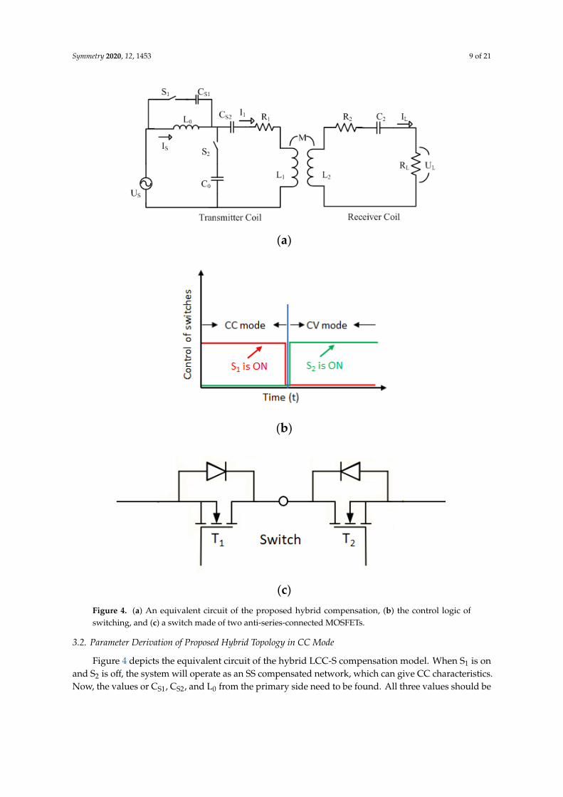
An equivalent circuit model of the proposed hybrid compensation is illustrated in Figure 4aand its switching schemes are shown in Figure 4b. As discussed earlier, the SS topology can achieveconstant current (CC) characteristics while LCC-S can achieve constant voltage (CV) characteristics. Inaddition, both the topologies provide ZPA. Therefore, a hybrid topology is adopted by combining theSS and LCC-S along with two switches from the primary side to realize the CC and CV characteristics.MOSFET IRF3710 was used for designing the switches due to its low conduction loss RDS of just23 mΩ. Each switch is made of two anti-series-linked MOSFETS as depicted in Figure 4c. Because ofhuge conduction losses of mechanical switching, the MOSFET switches are preferred. In addition,the motion of switches will be only once for each mode of operation; hence, the losses due to MOSFETswitching can be omitted.
3.1. Parameter Derivation of Proposed Hybrid Topology in CV Mode
When S2 is on and S1 is off, the system operates in an LCC-S compensated network; we can findthe values of C0 and L0 from Equation (27) as follows:
C0 =UL
US ω2M=
1ω2L0
(33)
L0 =USMUL
(34)
From Equation (19), we can get C2:
C2 =1
ω2L2(35)
CS2 can be achieved from Equation (17):
CS2 =1
ω2(L1 − L0)(36)
Now when the system operates in resonance frequency, we need a total of four parameter values:inductor, capacitor, capacitor from the primary side, and capacitor from the secondary side, which areL0, C0, CS2 from primary, and C2 from secondary.
Symmetry 2020, 12, 1453 9 of 21
Symmetry 2020, 12, x FOR PEER REVIEW 9 of 21
C = 1 ω (L − L ) (36)
Now when the system operates in resonance frequency, we need a total of four parameter values: inductor, capacitor, capacitor from the primary side, and capacitor from the secondary side, which are L0, C0, CS2 from primary, and C2 from secondary.
(a)
(b)
(c)
Figure 4. (a) An equivalent circuit of the proposed hybrid compensation, (b) the control logic of switching, and (c) a switch made of two anti-series-connected MOSFETs.
3.2. Parameter Derivation of Proposed Hybrid Topology in CC Mode
Figure 4 depicts the equivalent circuit of the hybrid LCC-S compensation model. When S1 is on and S2 is off, the system will operate as an SS compensated network, which can give CC characteristics. Now, the values or CS1, CS2, and L0 from the primary side need to be found. All three values should be equivalent to C1. In addition, C2 from the secondary side is also required; however, it will remain as given in (35).
I = − UjωM (37)
The following equation can be derived from Figure 3.
Figure 4. (a) An equivalent circuit of the proposed hybrid compensation, (b) the control logic ofswitching, and (c) a switch made of two anti-series-connected MOSFETs.
3.2. Parameter Derivation of Proposed Hybrid Topology in CC Mode
Figure 4 depicts the equivalent circuit of the hybrid LCC-S compensation model. When S1 is onand S2 is off, the system will operate as an SS compensated network, which can give CC characteristics.Now, the values or CS1, CS2, and L0 from the primary side need to be found. All three values should be
Symmetry 2020, 12, 1453 10 of 21
equivalent to C1. In addition, C2 from the secondary side is also required; however, it will remain asgiven in (35).
IL = −US
jωM12(37)
The following equation can be derived from Figure 4a.
jωL0jωCS1
jωL0 +1
jωCS1
+1
jωCS2=
1jωC1
(38)
By substituting Equation (11) into (17) and by using Equation (36), the value of C1 can be derivedas follows:
C1 =CS2
1 +ω2L0 CS2=
1ω2L1
(39)
By replacing the parameters from Equations (39) and (33)–(36) into (38), we get
CS1 =2
ω2L0(40)
By substituting Equation (37) into (34), L0 is obtained as given in Equation (41); after calculatingL0, CS1 can be calculated from Equation (40) and CS2 can calculated from Equation (36). In addition,C0 and C2 can be obtained using Equations (33) and (35).
L0 =ωM2IL
UL(41)
In order to design the parameters of the CC and CV mode operations, it is necessary to describethe mutual inductance amidst the coils. Therefore, to find the mutual inductance, the prototype of twocoils is realized and is provided in the next section.
3.3. Design of Two Symmetrical Coils
Before extracting the parameters of the proposed hybrid topology, it is essential to find theself-inductance of the Tx and Rx coils and the mutual inductance amidst the coils. The coils aresimulated and constructed to find the mutual inductance. The circular coil is a very prevalent designin resonant WPT systems due to its consolidated dimensions and largely constricted electromagnetic(EM) field behavior [25,26]. Hence, the circular coil is selected in this work and its simulation modeland a prototype is built as shown in Figure 5. Ferrite bars are also employed to intensify the magneticfield between the coils. Ten ferrite bars are used for Tx and Rx (each), having widths of 0.75 cm, heightsof 0.25 cm, and lengths of 11.5 cm. The same number of turns and ferrite bars are used to design thecoils in order to make them symmetrical in nature. The parameters of the simulated coil structure,including the self-inductances (L1 and L2) and mutual inductance (M) between the coils at a 13.5 cmairgap are calculated using the finite element method. Besides, the magnetic field is also calculatedbetween the coils as shown in Figure 5a. Enough red, yellow, and green color combinations of the fieldbetween the coils indicates that the intensity of the field is in a good range to achieve the high efficiencyof power transfer. Moreover, the self-inductance as well as mutual inductance of the prototype aremeasured according to the method provided in [27] using an RLC meter. It is noted that the prototypeuses litz wire with fabric insulation. In addition, Teflon (εr = 2.2) is used as coating for both coils.The diameter of the prototype coil’s wire is approximately 0.29 cm (including insulation) with total29 turns. After achieving the value of M, the remaining parameters to implement the hybrid topologyare determined in Section 3.

Symmetry 2020, 12, 1453 11 of 21Symmetry 2020, 12, x FOR PEER REVIEW 11 of 21
(a)
(b)
Figure 5. (a) The simulated coil structure and (b) a prototype of the circular coils along with its dimensions.
3.4. Parameter Derivations of Proposed Hybrid Topology
Figure 6 shows the flow diagram for derivation of parameters of hybrid topology to achieve CC and CV output features. Table 1 provides the parameters, which are calculated according to the flow chart. There is small variation in measured values as compared to calculated values. The variation occurs due to the realization of the prototype because of ±5% tolerance in hardware components. Therefore, to make a fair comparison between simulation and experimental results, only measured parameters are utilized for both the circuit simulations and the experiments. As the H-bridge power converter is utilized as a high frequency (HF) source during experiments, it is necessary to find the dc voltage required for the inverter. The H-bridge inverter provides a square waveform as the output. The square waveform contains always a lot of harmonics. Using Fourier series expansion, the output of H-bridge or full bridge inverter can be calculated using the following formula [28].
= 4 sin, , … ( = 1,3,4, … ) (42)
The simplified form of Fourier transform gives the dc input voltage required for the inverter, which is yielded as follows:
_ = √2 = 4 √2 = 0.9 (43)
Figure 5. (a) The simulated coil structure and (b) a prototype of the circular coils along withits dimensions.
3.4. Parameter Derivations of Proposed Hybrid Topology
Figure 6 shows the flow diagram for derivation of parameters of hybrid topology to achieve CCand CV output features. Table 1 provides the parameters, which are calculated according to the flowchart. There is small variation in measured values as compared to calculated values. The variationoccurs due to the realization of the prototype because of ±5% tolerance in hardware components.Therefore, to make a fair comparison between simulation and experimental results, only measuredparameters are utilized for both the circuit simulations and the experiments. As the H-bridge powerconverter is utilized as a high frequency (HF) source during experiments, it is necessary to find the dcvoltage required for the inverter. The H-bridge inverter provides a square waveform as the output.The square waveform contains always a lot of harmonics. Using Fourier series expansion, the outputof H-bridge or full bridge inverter can be calculated using the following formula [28].
US =4 Udc
π
∑∞
n=1,3,4...
sin nωtn
(n = 1, 3, 4, . . .) (42)
The simplified form of Fourier transform gives the dc input voltage required for the inverter,which is yielded as follows:
US_rms =USpeak to peak√
2=
4 Udc√
2 π= 0.9 Udc (43)
The DC voltage required for the inverter can be calculated by (43) using the given peak-to-peakvoltage, as provided in Table 2.

Symmetry 2020, 12, 1453 12 of 21
Symmetry 2020, 12, x FOR PEER REVIEW 12 of 21
The DC voltage required for the inverter can be calculated by (43) using the given peak-to-peak voltage, as provided in Table 2.
Table 1. Simulation and prototype results of coils.
Distance
between Coils Self-Inductance of Tx
Coil (L1) Self-Inductance of Rx
Coil (L2) Mutual Inductance between Coils (M)
Simulation Results 13.5 cm 203.15 uH 204.30 uH 27.355 uH
Measured Results 13.5 cm 202.70 uH 207.70 uH 27.275 uH
Figure 6. Flow diagram to implement the proposed hybrid topology.
Table 2 shows the designed and measured parameters. To implement the hybrid topology, initially, the operating frequency along with the desired voltage and current are selected. After that, the coils’ self-inductances and mutual inductance are measured according to the flow diagram, as shown in Figure 6. Thereafter, further compensation parameters such as capacitors, inductors, and the source voltage are calculated according to the derived equations of CC and CV models. Then, capacitor and inductors are soldered together in parallel and series, respectively, to obtain the values according to the design requirements. It is noted that, to provide a fair comparison between the simulations and experiments, all the prototype measured values were used in simulations.
Table 2. Designed parameters based on the given values in Table 1.
Parameter Name Designed Parameters Measured Parameters RL 6, 12, 18, 24 Ω 6, 12, 18, 24 Ω M 27.275 uH 27.275 uH
L1, L2 202.7 uH, 207.7 uH 202.7 uH, 207.7 uH R1, R2 0.3 Ω 0.3 Ω
F 160 kHz 160 kHz Desired Maximum UL (peak to peak) 48 V 48 V Desired Maximum IL (peak to peak) 2 A 2 A
L0 31.16 uH 31.10 uH CS1 63.50 nF 63.35 nF CS2 5.80 nF 5.95 nF C0 31.75 nF 31.62 nF C2 4.764 nF 4.86 nF
US (peak to peak) 54.84 V UDC = 43 V
Figure 6. Flow diagram to implement the proposed hybrid topology.
Table 1. Simulation and prototype results of coils.
Distancebetween Coils
Self-Inductance ofTx Coil (L1)
Self-Inductance ofRx Coil (L2)
Mutual Inductancebetween Coils (M)
SimulationResults 13.5 cm 203.15 uH 204.30 uH 27.355 uH
Measured Results 13.5 cm 202.70 uH 207.70 uH 27.275 uH
Table 2 shows the designed and measured parameters. To implement the hybrid topology, initially,the operating frequency along with the desired voltage and current are selected. After that, the coils’self-inductances and mutual inductance are measured according to the flow diagram, as shown inFigure 6. Thereafter, further compensation parameters such as capacitors, inductors, and the sourcevoltage are calculated according to the derived equations of CC and CV models. Then, capacitor andinductors are soldered together in parallel and series, respectively, to obtain the values according tothe design requirements. It is noted that, to provide a fair comparison between the simulations andexperiments, all the prototype measured values were used in simulations.
Table 2. Designed parameters based on the given values in Table 1.
Parameter Name Designed Parameters Measured Parameters
RL 6, 12, 18, 24 Ω 6, 12, 18, 24 ΩM 27.275 uH 27.275 uH
L1, L2 202.7 uH, 207.7 uH 202.7 uH, 207.7 uHR1, R2 0.3 Ω 0.3 Ω
F 160 kHz 160 kHzDesired Maximum UL (peak to peak) 48 V 48 VDesired Maximum IL (peak to peak) 2 A 2 A
L0 31.16 uH 31.10 uHCS1 63.50 nF 63.35 nFCS2 5.80 nF 5.95 nFC0 31.75 nF 31.62 nFC2 4.764 nF 4.86 nF
US (peak to peak) 54.84 V UDC = 43 V
4. Power Loss Analysis of CC and CV Mode
This section includes the derived equations of power losses. If the proposed topology is designedfor high-voltage applications like the battery charging of electric vehicles, then to measure the lossesof parasitic resistances of the coils, capacitances and inductances can be calculated in both modes of

Symmetry 2020, 12, 1453 13 of 21
operation as described below. In the previous section, the equations of efficiency have been derivedby considering negligible parasitic capacitances and resistances. However, in practical applications,this is not the case because all elements of the WPT system, including capacitor, inductors, and coils,etc., have losses. Therefore, the following derivations of the equations are useful for loss analysis inpractical applications.
4.1. Power Loss Analysis of CC Mode Operation
The circuits of the CC and CV modes are illustrated in Figure 7 and are divided in blocks to findout the efficiency and losses. For CC mode, the corresponding parasitic resistances of all elementsand coils are given in Figure 7a. R1 and R2 are the corresponding parasitic resistances of L1, and L2,respectively. Moreover, RL0, RCS1, and RCS2 are the corresponding parasitic resistances of L0, CS1,and CS2, respectively. In addition, RC0, and RC2 are the parasitic resistances of C0 and C2, respectively.In previous efficiency equations, as provided in Equations (13) and (32), the parasitic resistances ofcoils and all elements were ignored. However, here, detailed power loss equations are provided tofind the losses in the developed system. Both modes of operations including CC and CV are dividedinto blocks to simplify the derivations. As illustrated in Figure 7a,b, each block’s efficiency is derivedseparately and then combined with other blocks’ efficiencies.
ηC1 =RL
RC2 + R2 + RL(44)
ηC2 =Re(Zref_CC)
RCS2 + R1 + Re( 1
jωCS1RCS1
1jωCS1
+RCS1
)+ Re(Zref_CC)
(45)
Zref_CC =(ωM)2
RL + RCS2 + R2 + jωL2 +1
jωC2
(46)
ηCC = ηC1· ηC2 (47)
Symmetry 2020, 12, x FOR PEER REVIEW 13 of 21
4. Power Loss Analysis of CC and CV Mode
This section includes the derived equations of power losses. If the proposed topology is designed for high-voltage applications like the battery charging of electric vehicles, then to measure the losses of parasitic resistances of the coils, capacitances and inductances can be calculated in both modes of operation as described below. In the previous section, the equations of efficiency have been derived by considering negligible parasitic capacitances and resistances. However, in practical applications, this is not the case because all elements of the WPT system, including capacitor, inductors, and coils, etc., have losses. Therefore, the following derivations of the equations are useful for loss analysis in practical applications.
4.1. Power Loss Analysis of CC Mode Operation
The circuits of the CC and CV modes are illustrated in Figure 7 and are divided in blocks to find out the efficiency and losses. For CC mode, the corresponding parasitic resistances of all elements and coils are given in Figure 7a. R1 and R2 are the corresponding parasitic resistances of L1, and L2, respectively. Moreover, RL0, RCS1, and RCS2 are the corresponding parasitic resistances of L0, CS1, and CS2, respectively. In addition, RC0, and RC2 are the parasitic resistances of C0 and C2, respectively. In previous efficiency equations, as provided in Equations (13) and (32), the parasitic resistances of coils and all elements were ignored. However, here, detailed power loss equations are provided to find the losses in the developed system. Both modes of operations including CC and CV are divided into blocks to simplify the derivations. As illustrated in Figure 7a,b, each block’s efficiency is derived separately and then combined with other blocks’ efficiencies.
(a) (b)
Figure 7. Equivalent circuits of loss calculation in (a) constant-current (CC) mode and (b) constant-voltage (CV) mode.
η = RR + R + R (44)
η = Re Z _R + R + Re 1jωC R1jωC + R + Re Z _
(45)
Z _ = (ωM)R + R + R + jωL + 1jωC (46)
η = η . η (47)
Figure 7. Equivalent circuits of loss calculation in (a) constant-current (CC) mode and (b) constant-voltage(CV) mode.
It is noted that Zref_CC is the reflected impedance of a CC mode while Zref_CV defines the reflectedimpedance of CV mode. The equations of both reflected impedances are also provided, separately,as given in Equations (46) and (54). Moreover, the efficiency of each block is given the name of thatblock, such as ηC1 describing the efficiency of block C1 and so on.

Symmetry 2020, 12, 1453 14 of 21
4.2. Power Loss Analysis of CV Mode Operation
Figure 7b should be referred to find the losses in CV operational mode.
ηV1 =RL
RC2 + R2 + RL(48)
ηV2 =Re(Zref_CV)
RCS2 + R1 + Re(Zref_CV)(49)
ηV3 =(Re(Zref_CV) + RC0) |ZblockV3|
2
Re(ZblockV3) |ZblockV3|2 + (Re(Zref_CV) + RC0) + Re(Zref_CV) + |ZblockV3|
2 (50)
ηV4 =Re(ZblockV3)
RL0 + Re(ZblockV3)(51)
ZblockV3 =ZblockV2
(RC0 +
1jωC0
)ZblockV2 +
(RC0 +
1jωC0
) (52)
ZblockV2 = Zref_CV + R1 + jωL1 +1
jωCS2+ RCS2 (53)
Zref_CV =(ωM)2
RL + RCS2 + R2 + jωL2 +1
jωC2
(54)
ηCV = ηV1· ηV2·ηV3· ηV4 (55)
The above equations provided for the CC output and CV output modes can be effectively usedfor power losses and efficiency calculation of the proposed hybrid topology. The parasitic resistancevalues and component ratings are required to calculate the losses. In low-power applications, thevalues of parasitic resistance can be ignored, but in case of high-power applications, losses are crucialand therefore needs to be calculated.
5. Simulation Results and Analysis
This section comprises the operations in CC mode and in CV mode using a simulated circuit.To apply the proposed hybrid topology model, the measured data of the self-inductances and mutualinductance (M) amidst two symmetrical coils were used. All parameters along with their values arecalculated according to the derived equations and then given in Table 3.
Table 3. Peak values of voltage and currents.
CC, 6 Ω CC, 12 Ω CC, 18 Ω CC, 24 Ω CV, 24 Ω
Peak to Peak Output Current of Inverter (A) 0.652 A 1.019 1.402 1.780 1.726Peak to Peak Output Voltage (V) 12.03 V 23.79 35.14 46 45.44Peak to Peak Output Current (A) 2.005 A 1.983 1.952 1.917 1.852
Efficiency (%) 67.46% 84.42% 89.21% 90.33% 88.91%
The simulations are carried out starting from CC mode, meaning when the switch S1 is in the onposition and S2 is in the off position. The initial battery resistance is low; it increases during chargingas discussed in the Introduction section. Therefore, to test the proposed topology in CC behavior,an initial resistance of 6 Ω is applied. The zero-phase angle (ZPA) is also achieved as illustrated inFigure 8. Then, resistance is enhanced to 12 Ω, 18 Ω, and 24 Ω. The acquired current during all fourvalues of resistances is approximately 2 A, which is the desired current. The maximum desired voltagelimit is set as 48 V. When the maximum resistance value is simulated in CC mode, then maximumvoltage is achieved as depicted in Figure 9b. Afterward, the CC mode needs to be changed to CV

Symmetry 2020, 12, 1453 15 of 21
mode by switching on S2 and by turning off S1. Then, the system works in CV mode based onLCC-S topology. Vin indicates the input voltage waveforms, while Vout represents the output voltagewaveforms. Furthermore, I_probe1 shows the input current waveforms and I_probe2 illustrates the outputcurrent waveforms.
(a) (b)
(c) (d)
Figure 8. Input, output voltage, and current waveforms using RL: (a) 6 Ω, (b) 12 Ω, (c) 18 Ω, and (d) 24 Ω.
-40
-20
0
20
40
-60
60
-2
0
2
-4
4
time, msec
m1
m2m3
m4
m1time=Vin=54.838
4.002msecm2time=Vout=12.347
4.006msec
m3time=I_Probe1.i=0.594
4.001msecm4time=I_Probe2.i=2.052
4.013msec
-40
-20
0
20
40
-60
60
-2
0
2
-4
4
time, msec
m1
m2m3
m4
m1time=Vin=54.838
4.002msecm2time=Vout=24.555
4.006msec
m3time=I_Probe1.i=0.967
4.002msecm4time=I_Probe2.i=2.041
4.013msec
-40
-20
0
20
40
-60
60
-2
0
2
-4
4
time, msec
m1
m2m3
m4
m1time=Vin=54.838
4.002msecm2time=Vout=36.436
4.006msec
m3time=I_Probe1.i=1.408
4.002msecm4time=I_Probe2.i=2.025
4.013msec
-40
-20
0
20
40
-60
60
-2
0
2
-4
4
time, msec
m1m2
m3 m4
m1time=Vin=54.838
4.002msecm2time=Vout=48.262
4.006msec
m3time=I_Probe1.i=1.832
4.002msecm4time=I_Probe2.i=2.008
4.013msec ZPA
Figure 8. Input, output voltage, and current waveforms using RL: (a) 6 Ω, (b) 12 Ω, (c) 18 Ω, and (d) 24 Ω.
Figure 9 illustrates the CV characteristics based on LCC-S topology, and 48 V constant voltage isachievable in CV mode. A minor change occurs in the value due to the transient nature of a simulationanalysis. It is observed that the proposed hybrid topology is capable of working in CC and CV modesaccording to the desired output current and voltage. The zero-phase angle (ZPA) is also obtained inboth operational modes based on Equations (10) and (30). Vin, I_probe1 indicates the input voltage andcurrent, whereas Vout, I_probe2 represents the output waveforms of current and voltage. Moreover,the efficiency of the simulation can be calculated by the power output divided by the power input.The power input and output can be calculated by multiplying the corresponding peaks of the voltageand current values according to the waveforms. At 24 Ω, the efficiency of CC mode and CV mode are96.5% and 97.9%, respectively.

Symmetry 2020, 12, 1453 16 of 21
Figure 9. Input, output voltage, and current waveforms using RL = 24 Ω.
-40
-20
0
20
40
-60
60
-2
0
2
-4
4
time, msec
m1m2
m3 m4
m1time=Vin=54.822
4.002msecm2time=Vout=45.968
4.008msec
m3time=I_Probe1.i=1.678
4.002msecm4time=I_Probe2.i=1.928
4.014msec ZPA
Figure 9. Input, output voltage, and current waveforms using RL = 24 Ω.
Change of Mode from CC to CV Based on Estimation of UL
In the proposed topology, the change of mode can be obtained by estimating the maximum voltagevalue of the Rx side by using the value of maximum input current from the primary side. The maximuminput current can be calculated by multiplying the voltage gain with the desired maximum currentby the following expression: UL/US × desired output current = required input current, where thevoltage and currents are peak-to-peak values. The required input current is the maximum currentneeded for the transition of the operational mode from CC to CV. A current sensor is introduced inpractical applications from the primary side to detect the input current. Then, the sensed input currentcan be used for estimating the UL. Hence, the desired switching operation is obtainable without anycommunication link between the primary and secondary sides.
6. Experimental Results and Discussion
Figure 10 shows the experimental setup. H-bridge power inverter is utilized as a high-frequency(HF) source with an output square waveform. A variable load resistor is employed to change theresistance from 6 Ω to 24 Ω. During the switching mode from CC to CV, the small disturbance in thewaveform occurred; after that, the waveform stabilized. The experimental results of the waveform arepresented in Figures 11 and 12.
Symmetry 2020, 12, x FOR PEER REVIEW 16 of 21
Figure 9. Input, output voltage, and current waveforms using RL = 24 Ω.
Change of Mode from CC to CV Based on Estimation of UL
In the proposed topology, the change of mode can be obtained by estimating the maximum voltage value of the Rx side by using the value of maximum input current from the primary side. The maximum input current can be calculated by multiplying the voltage gain with the desired maximum current by the following expression: UL/US × desired output current = required input current, where the voltage and currents are peak-to-peak values. The required input current is the maximum current needed for the transition of the operational mode from CC to CV. A current sensor is introduced in practical applications from the primary side to detect the input current. Then, the sensed input current can be used for estimating the UL. Hence, the desired switching operation is obtainable without any communication link between the primary and secondary sides.
6. Experimental Results and Discussion
Figure 10 shows the experimental setup. H-bridge power inverter is utilized as a high-frequency (HF) source with an output square waveform. A variable load resistor is employed to change the resistance from 6 Ω to 24 Ω. During the switching mode from CC to CV, the small disturbance in the waveform occurred; after that, the waveform stabilized. The experimental results of the waveform are presented in Figures 11 and 12.
Figure 10. Experimental setup. Figure 10. Experimental setup.
Symmetry 2020, 12, 1453 17 of 21
(a) (b)
(c) (d)
Figure 11. Input voltage and current waveforms together with output waveforms in CC mode using different values of RL: (a) 6 Ω, (b) 12 Ω, (c) 18 Ω, and (d) 24 Ω.
Figure 12. Output waveforms in CV mode using RL = 24 Ω.
Figure 11. Input voltage and current waveforms together with output waveforms in CC mode usingdifferent values of RL: (a) 6 Ω, (b) 12 Ω, (c) 18 Ω, and (d) 24 Ω.
(a) (b)
(c) (d)
Figure 11. Input voltage and current waveforms together with output waveforms in CC mode using different values of RL: (a) 6 Ω, (b) 12 Ω, (c) 18 Ω, and (d) 24 Ω.
Figure 12. Output waveforms in CV mode using RL = 24 Ω.
Figure 12. Output waveforms in CV mode using RL = 24 Ω.
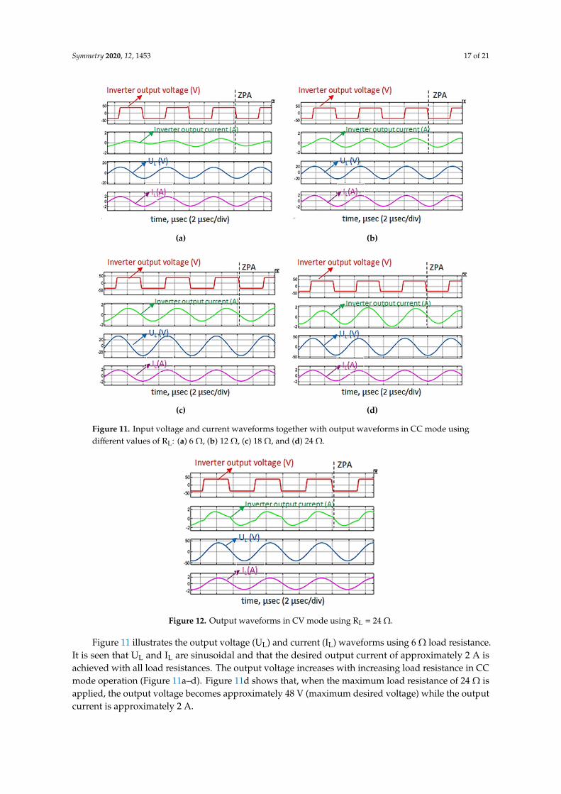
Figure 11 illustrates the output voltage (UL) and current (IL) waveforms using 6 Ω load resistance.It is seen that UL and IL are sinusoidal and that the desired output current of approximately 2 A isachieved with all load resistances. The output voltage increases with increasing load resistance in CCmode operation (Figure 11a–d). Figure 11d shows that, when the maximum load resistance of 24 Ω isapplied, the output voltage becomes approximately 48 V (maximum desired voltage) while the outputcurrent is approximately 2 A.
Symmetry 2020, 12, 1453 18 of 21
Figure 12 depicts the results of a CV mode operation, where output voltage remained constantas approximately 48 V, which is the desired voltage, and the output current is approximately 2 A.The result analysis presents that CC and CV characteristics are achievable with various loads, showingthe effectiveness of the proposed hybrid topology. The proposed equations are applicable for any typeof WPT system, i.e., low voltage or high voltage to obtain load-independent CC and CV features.
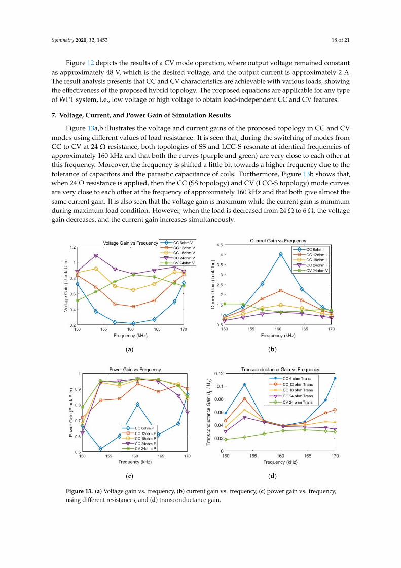
7. Voltage, Current, and Power Gain of Simulation Results
Figure 13a,b illustrates the voltage and current gains of the proposed topology in CC and CVmodes using different values of load resistance. It is seen that, during the switching of modes fromCC to CV at 24 Ω resistance, both topologies of SS and LCC-S resonate at identical frequencies ofapproximately 160 kHz and that both the curves (purple and green) are very close to each other atthis frequency. Moreover, the frequency is shifted a little bit towards a higher frequency due to thetolerance of capacitors and the parasitic capacitance of coils. Furthermore, Figure 13b shows that,when 24 Ω resistance is applied, then the CC (SS topology) and CV (LCC-S topology) mode curvesare very close to each other at the frequency of approximately 160 kHz and that both give almost thesame current gain. It is also seen that the voltage gain is maximum while the current gain is minimumduring maximum load condition. However, when the load is decreased from 24 Ω to 6 Ω, the voltagegain decreases, and the current gain increases simultaneously.Symmetry 2020, 12, x FOR PEER REVIEW 19 of 21
(a) (b)
(c) (d)
Figure 13. (a) Voltage gain vs. frequency, (b) current gain vs. frequency, (c) power gain vs. frequency, using different resistances, and (d) transconductance gain.
8. Conclusions
Wireless battery charging requires CC and CV input characteristics to improve the battery life cycle. This paper proposes a new hybrid topology to obtain load-independent CC and CV outputs. A comprehensive modeling and investigation of the symmetrical-coil-based WPT system are performed to design the parameters of the proposed compensation topology. Furthermore, the zero-phase angle (ZPA) is also ensured in both CC and CV operational modes to diminish the voltage-current rating of the input source and to improve the efficiency of the system. The power loss equations are also derived. As compared to other similar topologies, the proposed hybrid compensation is novel, reliable, and easy to implement, with only two additional switches from the primary side. It uses only a single capacitor from the secondary side, thus minimizing the number of components from the secondary side. Moreover, it utilizes the primary side switching control method, which can be achieved by sensing the input current. Therefore, the problem of communication link between the primary and secondary sides can be avoided. The proposed topology operates at a single resonance frequency, which is independent of the coupling factor and load settings. Therefore, it does not require adjustment of the frequency during switching operation; this is an extra benefit of the proposed design. A prototype is constructed to validate the simulation results and the theoretical analysis. The simulation results show that the maximum load efficiencies of 96.5% and 97.9% are obtained in CC and CV modes, respectively, while the maximum load efficiencies of the experimental results are 90.33% and 88.91% in CC and CV modes, respectively. Overall, it can be concluded that the maximum efficiency of around 90% is achieved when a maximum power of around 96 W peak to peak was delivered to the load at 13.5 cm distance. It is
Figure 13. (a) Voltage gain vs. frequency, (b) current gain vs. frequency, (c) power gain vs. frequency,using different resistances, and (d) transconductance gain.

Symmetry 2020, 12, 1453 19 of 21
Figure 13c shows that the maximum power gain is achievable using 24 Ω resistance in CC and CVmodes, which is above 0.9. In addition, the power gain using 12 Ω and 18 Ω resistance is almost thesame as that of the 24 Ω gain at approximately 160 kHz frequency; however, the power gain dropsbelow 0.9 using 6 Ω resistance, as illustrated in the blue curve with diamond markers in Figure 13c.Therefore, it can be deduced that the low load resistance provides less efficiency as compared to thehigh load resistance. Moreover, the operating frequency range is increased at high resistance values,which shows that, when 18 Ω and 24 Ω resistances are applied, high power gain can be obtainedbetween the frequencies of 154 kHz to 168 kHz. Therefore, even some variation in the resonancefrequency does not decrease the efficiency, especially at high load resistances. However, using alow resistance value, the operating frequency should be equal to the resonance frequency; otherwise,the efficiency will be affected.
8. Conclusions
Wireless battery charging requires CC and CV input characteristics to improve the battery lifecycle. This paper proposes a new hybrid topology to obtain load-independent CC and CV outputs.A comprehensive modeling and investigation of the symmetrical-coil-based WPT system are performedto design the parameters of the proposed compensation topology. Furthermore, the zero-phase angle(ZPA) is also ensured in both CC and CV operational modes to diminish the voltage-current ratingof the input source and to improve the efficiency of the system. The power loss equations are alsoderived. As compared to other similar topologies, the proposed hybrid compensation is novel, reliable,and easy to implement, with only two additional switches from the primary side. It uses only a singlecapacitor from the secondary side, thus minimizing the number of components from the secondary side.Moreover, it utilizes the primary side switching control method, which can be achieved by sensingthe input current. Therefore, the problem of communication link between the primary and secondarysides can be avoided. The proposed topology operates at a single resonance frequency, which isindependent of the coupling factor and load settings. Therefore, it does not require adjustment of thefrequency during switching operation; this is an extra benefit of the proposed design. A prototype isconstructed to validate the simulation results and the theoretical analysis. The simulation results showthat the maximum load efficiencies of 96.5% and 97.9% are obtained in CC and CV modes, respectively,while the maximum load efficiencies of the experimental results are 90.33% and 88.91% in CC andCV modes, respectively. Overall, it can be concluded that the maximum efficiency of around 90% isachieved when a maximum power of around 96 W peak to peak was delivered to the load at 13.5 cmdistance. It is worth mentioning that the proposed compensation topology is suitable for fixed-distancestationary charging applications because, due to distance variations or misalignments, there may bechanges in the output voltages and currents.
Author Contributions: Conceptualization, M.R.; funding acquisition, P.N.; investigation, M.R.; methodology, M.R.and Z.B.; supervision, P.N.; writing—original draft, M.R.; writing—review and editing, P.N. and Z.B. All authorshave read and agreed to the published version of the manuscript.
Funding: This research was funded by YUTP Grant having Cost Centre 015LCO-024.
Acknowledgments: The authors would like to thank the Universiti Teknologi PETRONAS for supporting thisresearch work.
Conflicts of Interest: The authors declare no conflict of interest.
References
1. Xiao, C.; Cheng, D.; Wei, K. An LCC-C compensated wireless charging system for implantable cardiacpacemakers: Theory, experiment, and safety evaluation. IEEE Trans. Power Electron. 2017, 33, 4894–4905.[CrossRef]
2. Vilathgamuwa, D.M.; Sampath, J.P.K. Wireless power transfer (WPT) for electric vehicles (EVs)—Present andfuture trends. In Plug in Electric Vehicles in Smart Grids; Springer: Berlin, Germany, 2015; pp. 33–60.

Symmetry 2020, 12, 1453 20 of 21
3. Li, Y.; Mai, R.; Lu, L.; He, Z. Active and reactive currents decomposition-based control of angle and magnitudeof current for a parallel multiinverter IPT system. IEEE Trans. Power Electron. 2016, 32, 1602–1614. [CrossRef]
4. Liu, C.; Jiang, C.; Song, J.; Chau, K.T. An effective sandwiched wireless power transfer system for chargingimplantable cardiac pacemaker. IEEE Trans. Ind. Electron. 2018, 66, 4108–4117. [CrossRef]
5. Yang, L.; Li, X.; Liu, S.; Xu, Z.; Cai, C.; Guo, P. Analysis and Design of Three-Coil Structure WPT System withConstant Output Current and Voltage for Battery Charging Applications. IEEE Access 2019, 7, 87334–87344.[CrossRef]
6. Qu, X.; Han, H.; Wong, S.C.; Chi, K.T.; Chen, W. Hybrid IPT topologies with constant current or constantvoltage output for battery charging applications. IEEE Trans. Power Electron. 2015, 30, 6329–6337. [CrossRef]
7. Song, K.; Li, Z.; Jiang, J.; Zhu, C. Constant current/voltage charging operation for series–series andseries–parallel compensated wireless power transfer systems employing primary-side controller. IEEE Trans.Power Electron. 2017, 33, 8065–8080. [CrossRef]
8. Zhang, W.; Mi, C.C. Compensation topologies of high-power wireless power transfer systems. IEEE Trans.Veh. Technol. 2015, 65, 4768–4778. [CrossRef]
9. Li, Y.L.; Sun, Y.; Dai, X. /spl mu/-Synthesis for Frequency Uncertainty of the ICPT System. IEEE Trans.Ind. Electron. 2011, 60, 291–300. [CrossRef]
10. Swain, A.; Almakhles, D.; Neath, M.J.; Nasiri, A. Robust H∞ output feedback control of bidirectionalinductive power transfer systems. Arch. Control Sci. 2017, 27, 41–62. [CrossRef]
11. Xia, C.; Wang, W.; Chen, G.; Wu, X.; Zhou, S.; Sun, Y. Robust control for the relay ICPT system under externaldisturbance and parametric uncertainty. IEEE Trans. Control Syst. Technol. 2016, 25, 2168–2175. [CrossRef]
12. Zhang, W.; Wong, S.-C.; Chi, K.T.; Chen, Q. Analysis and comparison of secondary series-andparallel-compensated inductive power transfer systems operating for optimal efficiency and load-independentvoltage-transfer ratio. IEEE Trans. Power Electron. 2013, 29, 2979–2990. [CrossRef]
13. Rehman, M.; Nallagownden, P.; Baharudin, Z. Efficiency investigation of SS and SP compensation topologiesfor wireless power transfer. Int. J. Power Electron. Drive Syst. 2019, 10, 2157–2164. [CrossRef]
14. Li, S.; Li, W.; Deng, J.; Nguyen, T.D.; Mi, C.C. A double-sided LCC compensation network and its tuningmethod for wireless power transfer. IEEE Trans. Veh. Technol. 2014, 64, 2261–2273. [CrossRef]
15. Esteban, B.; Sid-Ahmed, M.; Kar, N.C. A comparative study of power supply architectures in wireless EVcharging systems. IEEE Trans. Power Electron. 2015, 30, 6408–6422. [CrossRef]
16. Yao, Y.; Wang, Y.; Liu, X.; Lin, F.; Xu, D. A Novel Parameter Tuning Method for a Double-Sided LCLCompensated WPT System with Better Comprehensive Performance. IEEE Trans. Power Electron. 2017, 33,8525–8536. [CrossRef]
17. Alam, M.; Mekhilef, S.; Bassi, H.; Rawa, M. Analysis of LC-LC2 Compensated Inductive Power Transfer forHigh Efficiency and Load Independent Voltage Gain. Energies 2018, 11, 2883. [CrossRef]
18. Yan, Z.; Zhang, Y.; Song, B.; Zhang, K.; Kan, T.; Mi, C. An LCC-P compensated wireless power transfersystem with a constant current output and reduced receiver size. Energies 2019, 12, 172. [CrossRef]
19. Liu, X.; Clare, L.; Yuan, X.; Wang, C.; Liu, J. A design method for making an lcc compensation two-coil wirelesspower transfer system more energy efficient than an ss counterpart. Energies 2017, 10, 1346. [CrossRef]
20. Zhang, W.; Wong, S.-C.; Chi, K.T.; Chen, Q. Design for efficiency optimization and voltage controllability ofseries–series compensated inductive power transfer systems. IEEE Trans. Power Electron. 2013, 29, 191–200.[CrossRef]
21. Auvigne, C.; Germano, P.; Ladas, D.; Perriard, Y. A dual-topology ICPT applied to an electric vehicle batterycharger. In Proceedings of the IEEE 2012 XXth International Conference on Electrical Machines, Marseille,France, 2–5 September 2012; pp. 2287–2292.
22. Mai, R.; Chen, Y.; Li, Y.; Zhang, Y.; Cao, G.; He, Z. Inductive power transfer for massive electric bicyclescharging based on hybrid topology switching with a single inverter. IEEE Trans. Power Electron. 2017, 32,5897–5906. [CrossRef]
23. Li, Y.; Xu, Q.; Lin, T.; Hu, J.; He, Z.; Mai, R. Analysis and design of load-independent output current oroutput voltage of a three-coil wireless power transfer system. IEEE Trans. Transp. Electrif. 2018, 4, 364–375.[CrossRef]
24. Chen, Y.; Kou, Z.; Zhang, Y.; He, Z.; Mai, R.; Cao, G. Hybrid topology with configurable charge current andcharge voltage output-based WPT charger for massive electric bicycles. IEEE J. Emerg. Sel. Top. Power Electron.2017, 6, 1581–1594. [CrossRef]

Symmetry 2020, 12, 1453 21 of 21
25. Shi, X.; Qi, C.; Qu, M.; Ye, S.; Wang, G.; Sun, L.; Yu, Z. Effects of coil shapes on wireless power transfer viamagnetic resonance coupling. J. Electromagn. Waves Appl. 2014, 28, 1316–1324. [CrossRef]
26. McDonough, M.; Fahimi, B. Comparison between circular and square coils for use in wireless powertransmission. In Proceedings of the 9th IET International Conference on Computation in Electromagnetics,London, UK, 31 March–1 April 2014.
27. Eftekhar, M.G.; Ouyang, Z.; Andersen, M.A.; Andersen, P.B.; Ribeiro, L.A.D.S.; Schaltz, E. Efficiency studyof vertical distance variations in wireless power transfer for e-mobility. IEEE Trans. Magn. 2016, 52, 1–4.[CrossRef]
28. Kim, S.-H. Electric Motor Control: DC, AC, and BLDC Motors; Elsevier: Amsterdam, The Netherlands, 2017.
© 2020 by the authors. Licensee MDPI, Basel, Switzerland. This article is an open accessarticle distributed under the terms and conditions of the Creative Commons Attribution(CC BY) license (http://creativecommons.org/licenses/by/4.0/).


![12 Switch Zero-Inductor Voltage Converter Topology...Bus Architecture, to achieve this stepdown at high efficiency [6][7]. The topology proposed in this paper is a novel topology for](https://img.dokumen.tips/doc/110x75/5fe7a75918fdc7779a057bf3/12-switch-zero-inductor-voltage-converter-topology-bus-architecture-to-achieve.jpg)


![[XLS] · Web viewAL3Z AU2Z WPT-1090 BL3Z F4AZ 15A416 9E5Z K WPT-1161 8L3Z F5SZ 9F479 UB WPT-992 8C2Z BHAB WPT-1147 F5TZ AU5Z WPT-1089 16611B08 16611B09 BC3Z F5CZ XF3Z WPT-1001 NUB](https://img.dokumen.tips/doc/110x75/5af9707e7f8b9aac248e66a3/xls-viewal3z-au2z-wpt-1090-bl3z-f4az-15a416-9e5z-k-wpt-1161-8l3z-f5sz-9f479-ub.jpg)
![BepiColombo/MMO: PWI/WPT-S PWI Kanazawa Meeting [Mar 2006] WPT-S MEFISTO-S [WPT: Team members] Lead Co-IY. Kasaba (JAXA) ManufacturerNIPPI [PWI] K. Ishisaka,](https://img.dokumen.tips/doc/110x75/56649ee85503460f94bf97fe/bepicolombommo-pwiwpt-s-pwi-kanazawa-meeting-mar-2006-wpt-s-mefisto-s.jpg)


