Embed Size (px)
Citation preview
Design, Control and Application of Modular Multilevel Converters for
HVDC Transmission Systems
Chapter 2 Main-Circuit Design
by Kamran Sharifabadi, Lennart Harnefors,
Hans-Peter Nee, Staffan Norrga, Remus Teodorescu ISBN-10: 1118851560 Copyright Wiley 2016
Outline Main-Circuit Design
• Power Semiconductor Devices for MMCs • Submodule Capacitors • Arm Inductors • Submodule Configurations • Choice of Main-Circuit Parameters • Handling of Redundant and Faulty submodules • Auxiliary Power Supplies for Submodules
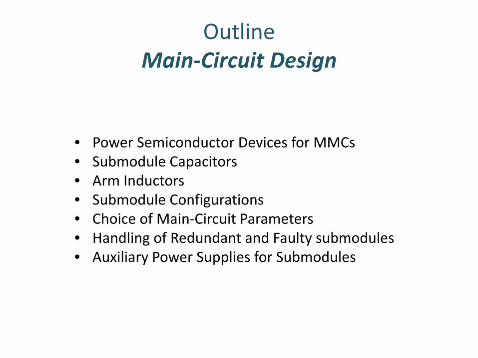
Power Semiconductor Devices for MMCs
• Very low switching frequency (approx. 150 Hz) • Low voltage drop (requirement) • Minimize complexity by using high-voltage submodules
High-voltage device with low conduction losses
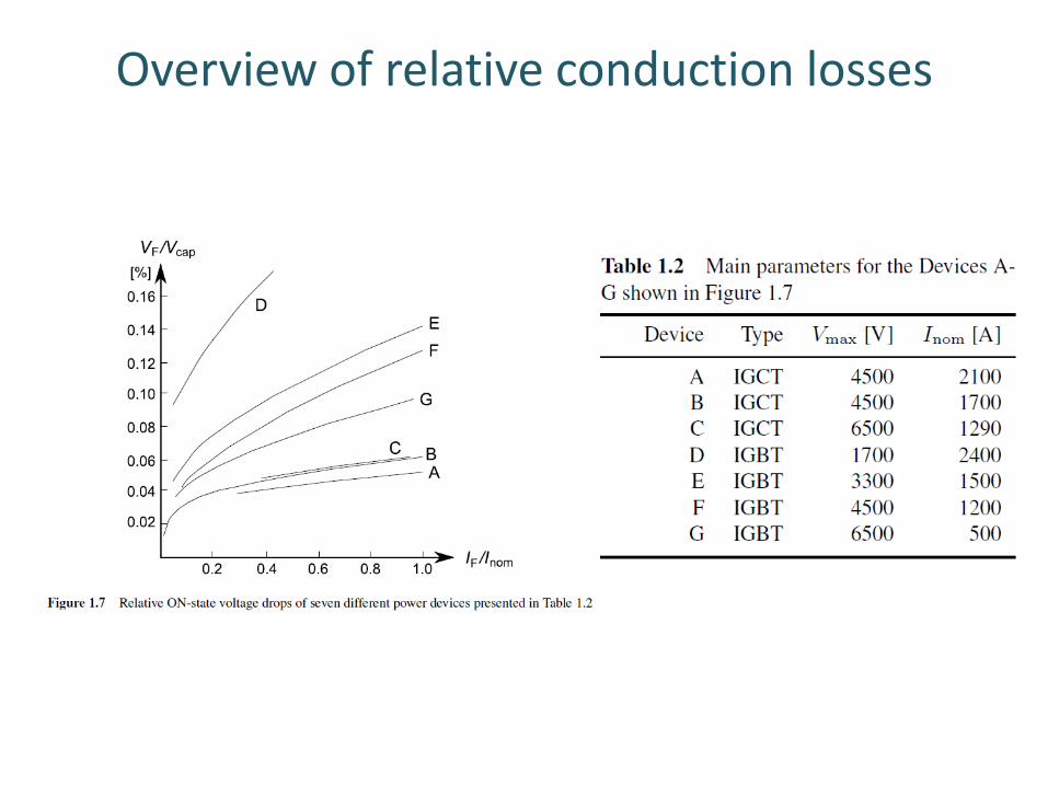
Overview of relative conduction losses
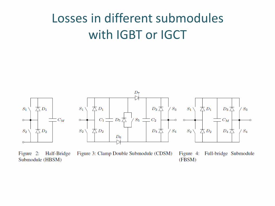
Losses in different submodules with IGBT or IGCT
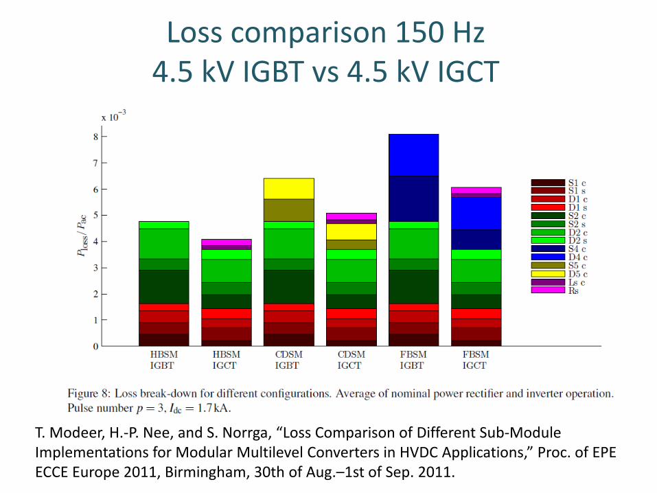
Loss comparison 150 Hz 4.5 kV IGBT vs 4.5 kV IGCT
T. Modeer, H.-P. Nee, and S. Norrga, “Loss Comparison of Different Sub-Module Implementations for Modular Multilevel Converters in HVDC Applications,” Proc. of EPE ECCE Europe 2011, Birmingham, 30th of Aug.–1st of Sep. 2011.
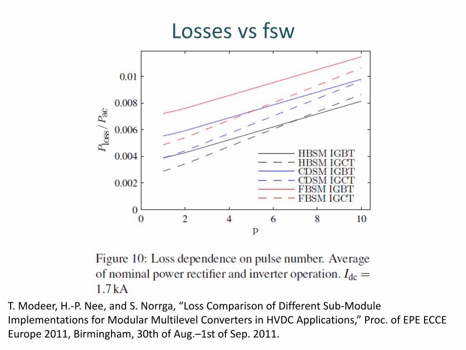
Losses vs fsw
T. Modeer, H.-P. Nee, and S. Norrga, “Loss Comparison of Different Sub-Module Implementations for Modular Multilevel Converters in HVDC Applications,” Proc. of EPE ECCE Europe 2011, Birmingham, 30th of Aug.–1st of Sep. 2011.
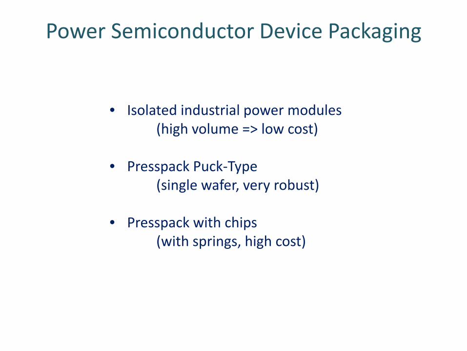
Power Semiconductor Device Packaging
• Isolated industrial power modules (high volume => low cost)
• Presspack Puck-Type (single wafer, very robust)
• Presspack with chips (with springs, high cost)
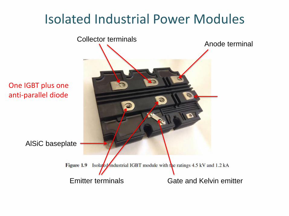
Isolated Industrial Power Modules Collector terminals
Emitter terminals
Anode terminal
Gate and Kelvin emitter
AlSiC baseplate
One IGBT plus one anti-parallel diode
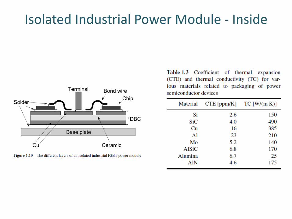
Isolated Industrial Power Module - Inside
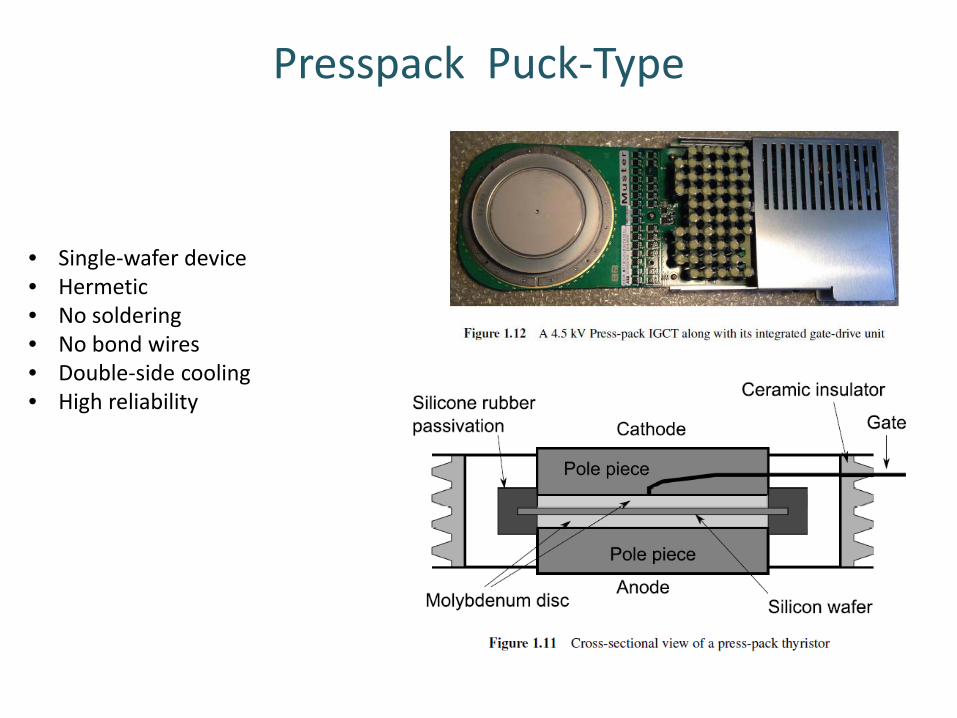
Presspack Puck-Type
• Single-wafer device • Hermetic • No soldering • No bond wires • Double-side cooling • High reliability
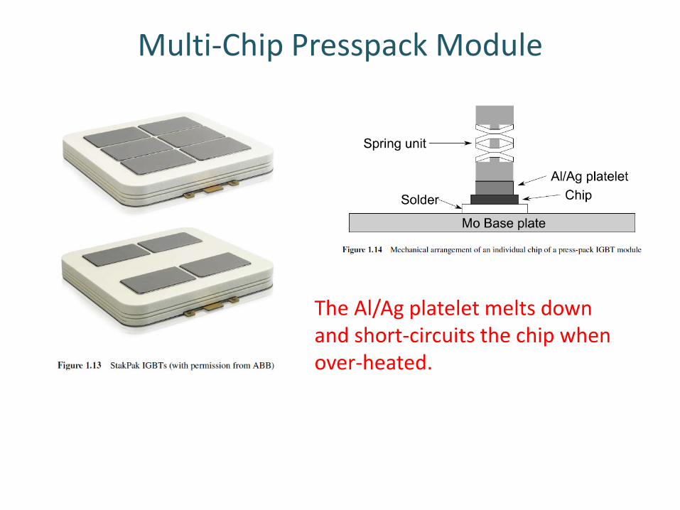
Multi-Chip Presspack Module
The Al/Ag platelet melts down and short-circuits the chip when over-heated.
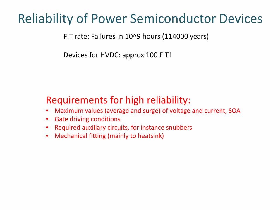
Reliability of Power Semiconductor Devices FIT rate: Failures in 10^9 hours (114000 years) Devices for HVDC: approx 100 FIT!
Requirements for high reliability: • Maximum values (average and surge) of voltage and current, SOA • Gate driving conditions • Required auxiliary circuits, for instance snubbers • Mechanical fitting (mainly to heatsink)
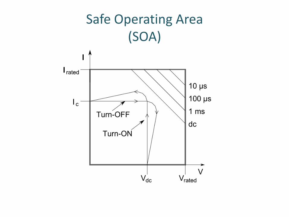
Safe Operating Area (SOA)
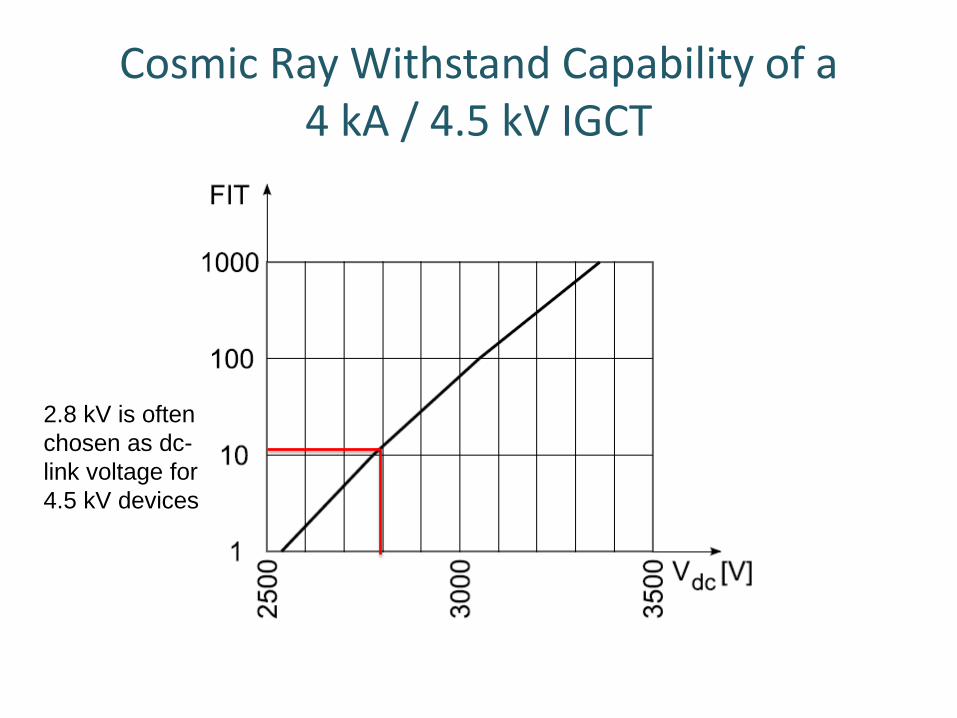
Cosmic Ray Withstand Capability of a 4 kA / 4.5 kV IGCT
2.8 kV is often chosen as dc- link voltage for 4.5 kV devices
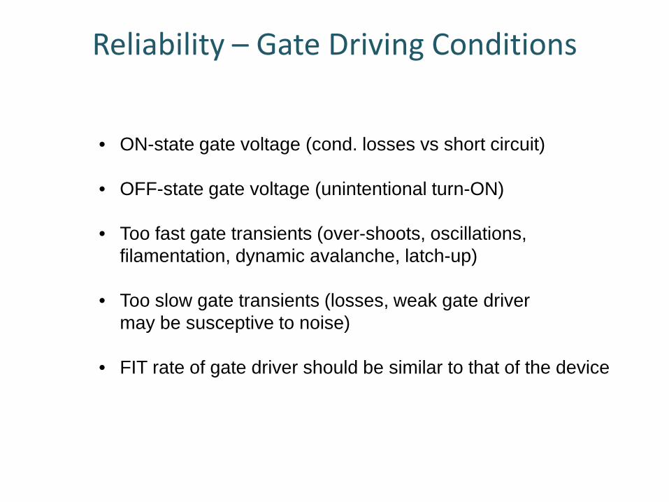
Reliability – Gate Driving Conditions
• ON-state gate voltage (cond. losses vs short circuit)
• OFF-state gate voltage (unintentional turn-ON)
• Too fast gate transients (over-shoots, oscillations, filamentation, dynamic avalanche, latch-up)
• Too slow gate transients (losses, weak gate driver may be susceptive to noise)
• FIT rate of gate driver should be similar to that of the device
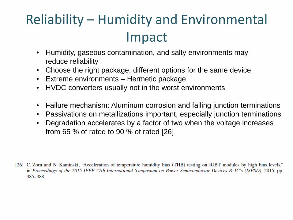
Reliability – Humidity and Environmental Impact
• Humidity, gaseous contamination, and salty environments may reduce reliability
• Choose the right package, different options for the same device • Extreme environments – Hermetic package • HVDC converters usually not in the worst environments
• Failure mechanism: Aluminum corrosion and failing junction terminations • Passivations on metallizations important, especially junction terminations • Degradation accelerates by a factor of two when the voltage increases
from 65 % of rated to 90 % of rated [26]
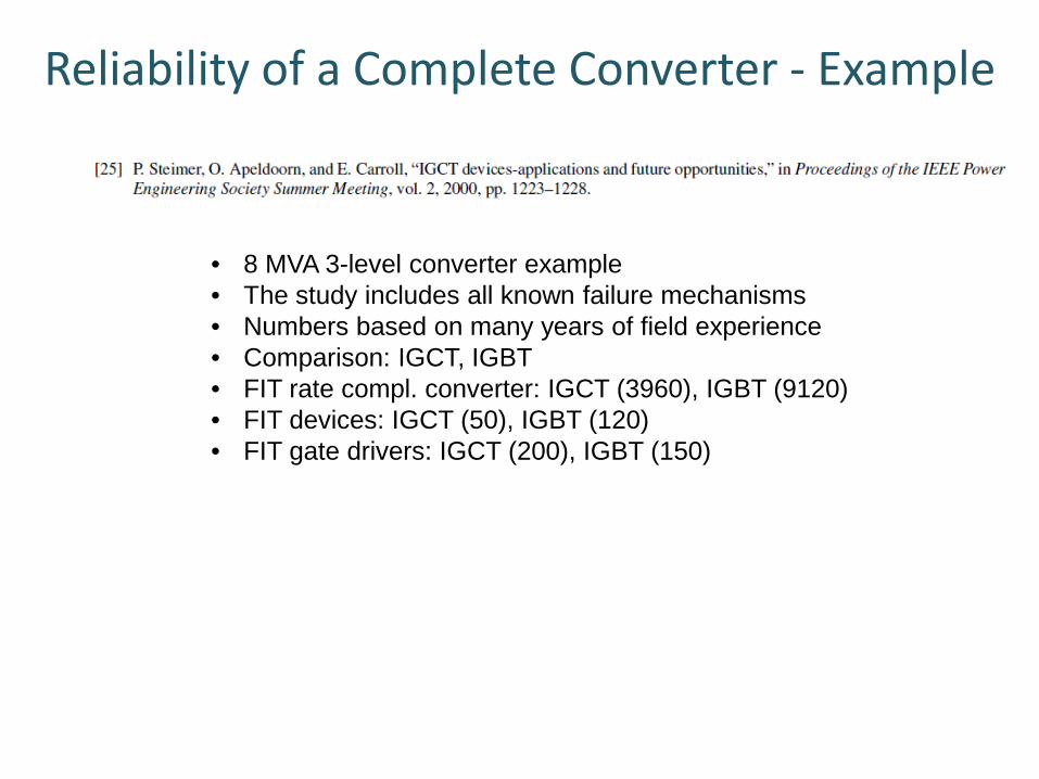
Reliability of a Complete Converter - Example
• 8 MVA 3-level converter example • The study includes all known failure mechanisms • Numbers based on many years of field experience • Comparison: IGCT, IGBT • FIT rate compl. converter: IGCT (3960), IGBT (9120) • FIT devices: IGCT (50), IGBT (120) • FIT gate drivers: IGCT (200), IGBT (150)
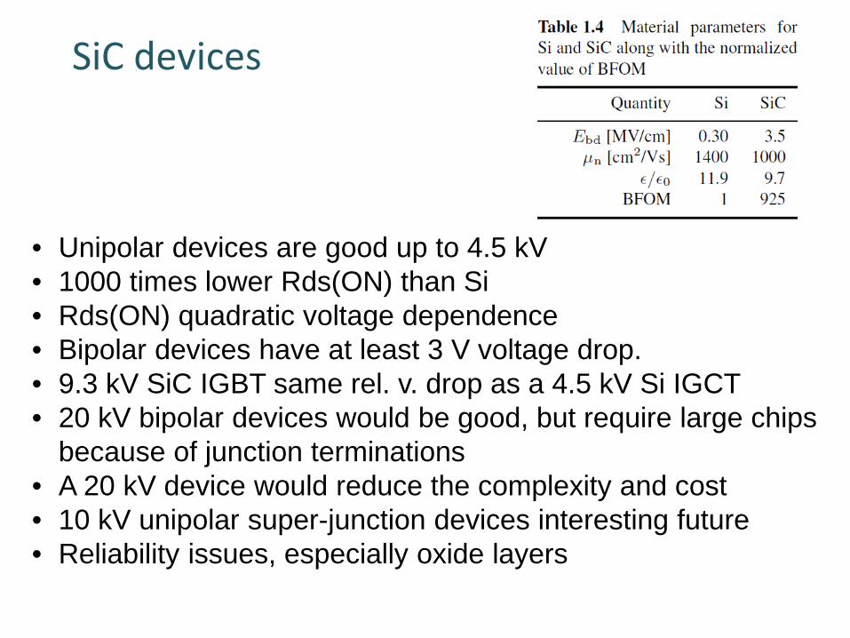
SiC devices
• Unipolar devices are good up to 4.5 kV • 1000 times lower Rds(ON) than Si • Rds(ON) quadratic voltage dependence • Bipolar devices have at least 3 V voltage drop. • 9.3 kV SiC IGBT same rel. v. drop as a 4.5 kV Si IGCT • 20 kV bipolar devices would be good, but require large chips
because of junction terminations • A 20 kV device would reduce the complexity and cost • 10 kV unipolar super-junction devices interesting future • Reliability issues, especially oxide layers
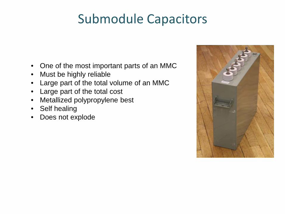
Submodule Capacitors
• One of the most important parts of an MMC • Must be highly reliable • Large part of the total volume of an MMC • Large part of the total cost • Metallized polypropylene best • Self healing • Does not explode

Submodule Capacitors – Design and Fabrication
• Voltages up to 10 kV • Cuboid-shaped housing of aluminum
or non-magnetic stainless steel • Bushings that can withstand voltages
in the kilovolt range • Voids between active parts and housing
filled with polyurethane resin • Two polypropylene films with vacuum-
deposited metal (Al, Zn), 1 micrometer • The thickness of plastic layers –
voltage dependent
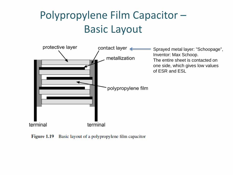
Polypropylene Film Capacitor – Basic Layout
Sprayed metal layer: ”Schoopage”, Inventor: Max Schoop. The entire sheet is contacted on one side, which gives low values of ESR and ESL
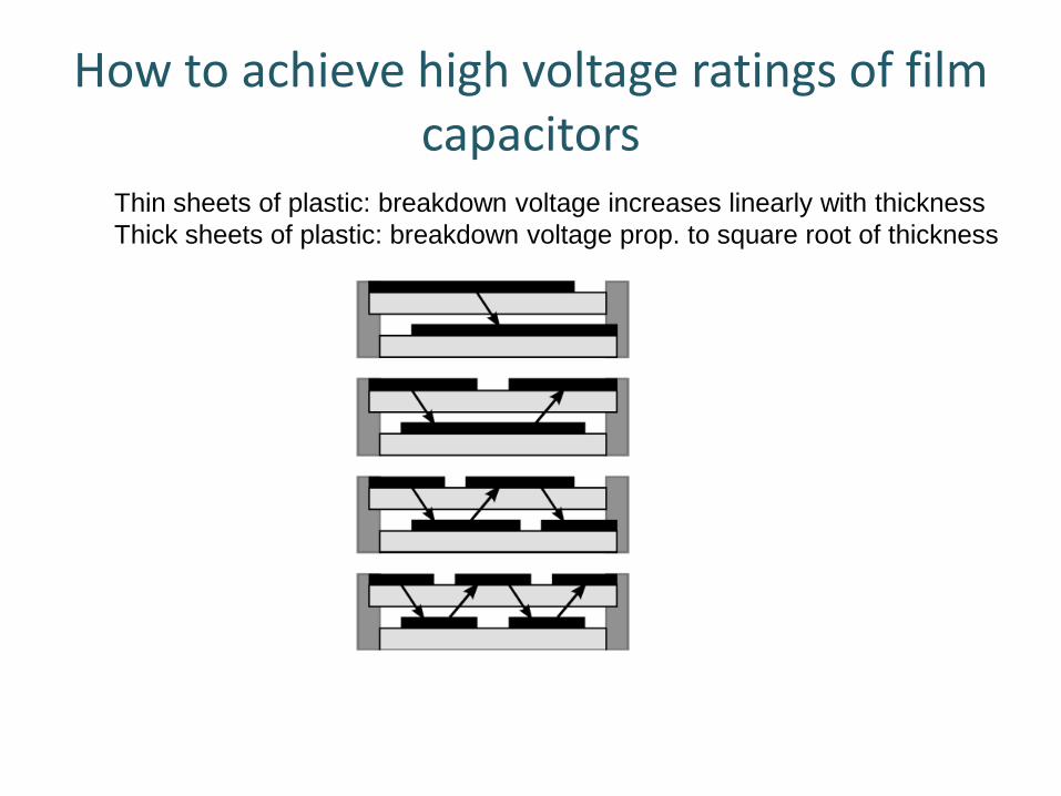
How to achieve high voltage ratings of film capacitors
Thin sheets of plastic: breakdown voltage increases linearly with thickness Thick sheets of plastic: breakdown voltage prop. to square root of thickness
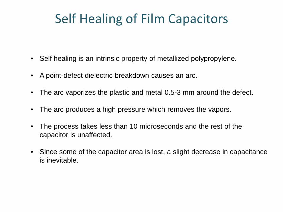
Self Healing of Film Capacitors
• Self healing is an intrinsic property of metallized polypropylene.
• A point-defect dielectric breakdown causes an arc.
• The arc vaporizes the plastic and metal 0.5-3 mm around the defect.
• The arc produces a high pressure which removes the vapors.
• The process takes less than 10 microseconds and the rest of the capacitor is unaffected.
• Since some of the capacitor area is lost, a slight decrease in capacitance is inevitable.
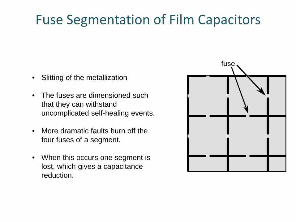
Fuse Segmentation of Film Capacitors
• Slitting of the metallization
• The fuses are dimensioned such that they can withstand uncomplicated self-healing events.
• More dramatic faults burn off the four fuses of a segment.
• When this occurs one segment is lost, which gives a capacitance reduction.
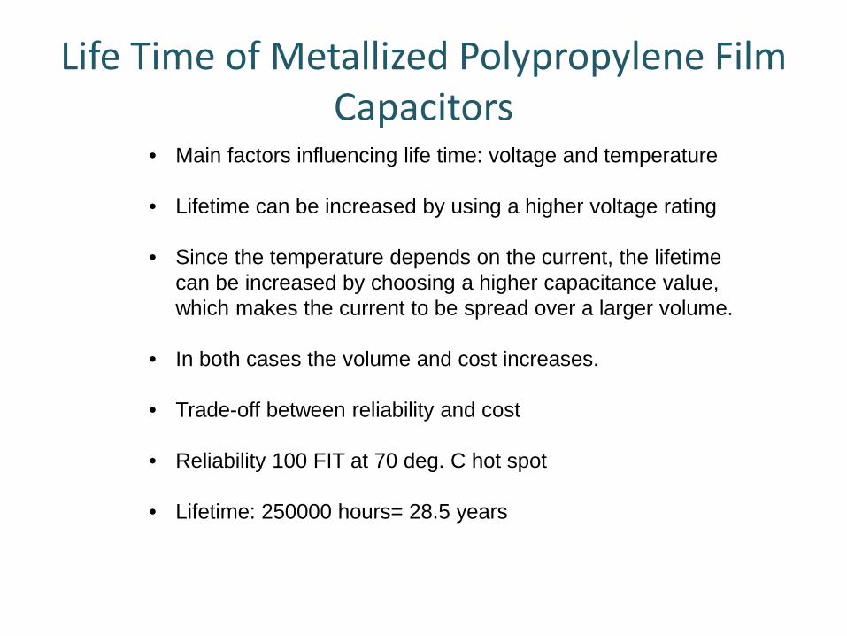
Life Time of Metallized Polypropylene Film Capacitors
• Main factors influencing life time: voltage and temperature
• Lifetime can be increased by using a higher voltage rating
• Since the temperature depends on the current, the lifetime can be increased by choosing a higher capacitance value, which makes the current to be spread over a larger volume.
• In both cases the volume and cost increases.
• Trade-off between reliability and cost
• Reliability 100 FIT at 70 deg. C hot spot
• Lifetime: 250000 hours= 28.5 years
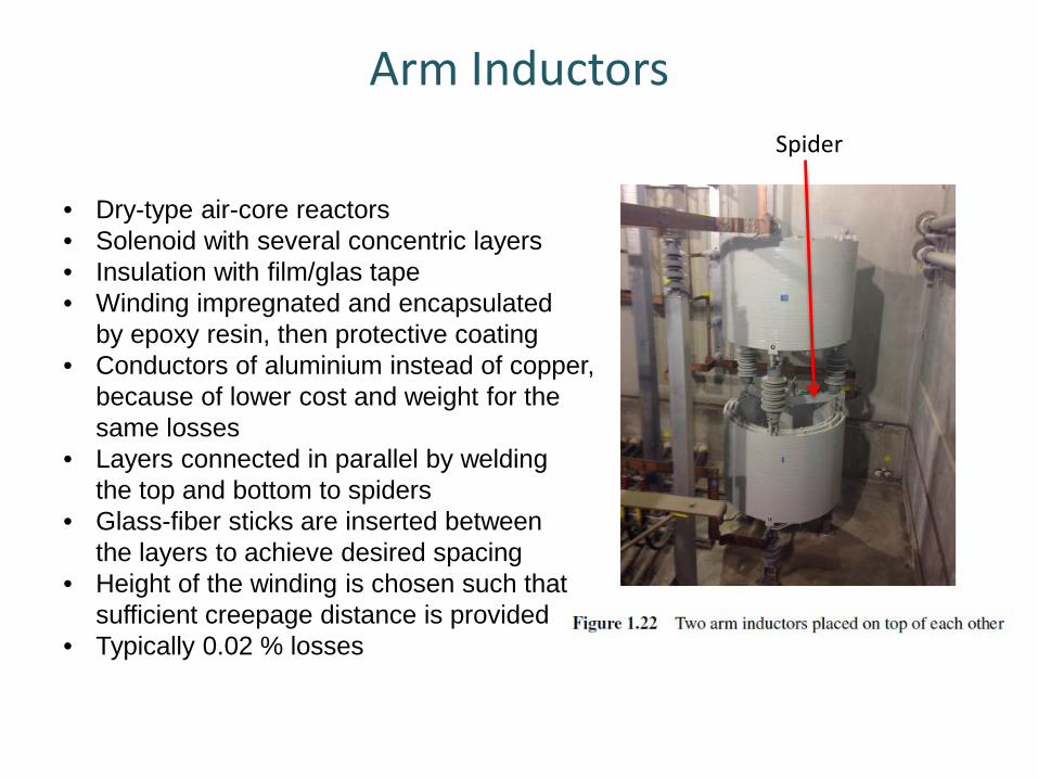
Arm Inductors
• Dry-type air-core reactors • Solenoid with several concentric layers • Insulation with film/glas tape • Winding impregnated and encapsulated
by epoxy resin, then protective coating • Conductors of aluminium instead of copper,
because of lower cost and weight for the same losses
• Layers connected in parallel by welding the top and bottom to spiders
• Glass-fiber sticks are inserted between the layers to achieve desired spacing
• Height of the winding is chosen such that sufficient creepage distance is provided
• Typically 0.02 % losses
Spider
Submodule Configurations
• General remarks • Existing half-bridge realizations • Clamped single-submodule • Clamped double-submodule • Unipolar-voltage full-bridge submodule • Five-level cross-connected submodule • Three-level cross-connected submodule • Double submodule • Semi-full-bridge submodule • Soft-switching submodules
General Remarks Regarding Submodule Configurations
• So far, only half-bridges (HB), lowest losses, lowest costs • Full-bridge (FB) can provide counter voltage in case of dc fault,
control fault current, 2 times semiconductor cost, 80 % higher losses than HB • Hybrid, 50% HB+50% FB, same SC properties as FB • Clamped single and Clamped double-submodules can handle dc faults, but
cannot control the fault current. Both are intermediate to HB and FB with respect to losses and semiconductor costs.
• Five-level and three-level cross-connected submodules can also handle dc faults. • Unipolar full-bridge submodule similar to clamped single-submodule • Double submodule can reduce the capacitor size • Semi-full-bridge submodule extension of the Clamped double-submodule but with
the possibility to reduce the capacitor size • Soft-switching submodules with thyristors can increase the submodule voltage,
reduce the cost, and reduce the losses

Siemens Half-Bridge Realization Source: Siemens
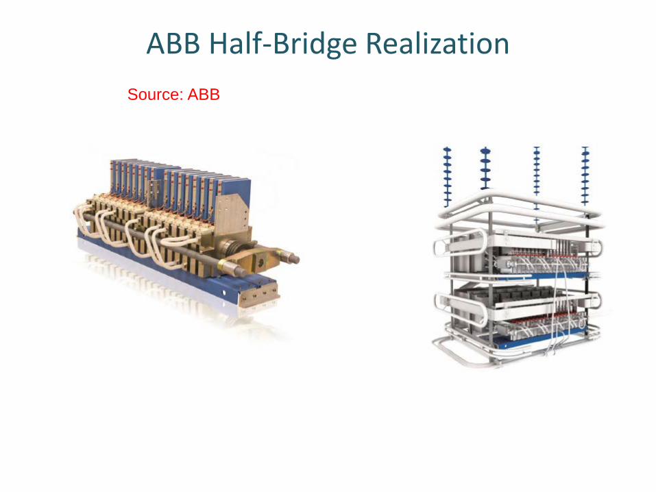
ABB Half-Bridge Realization Source: ABB
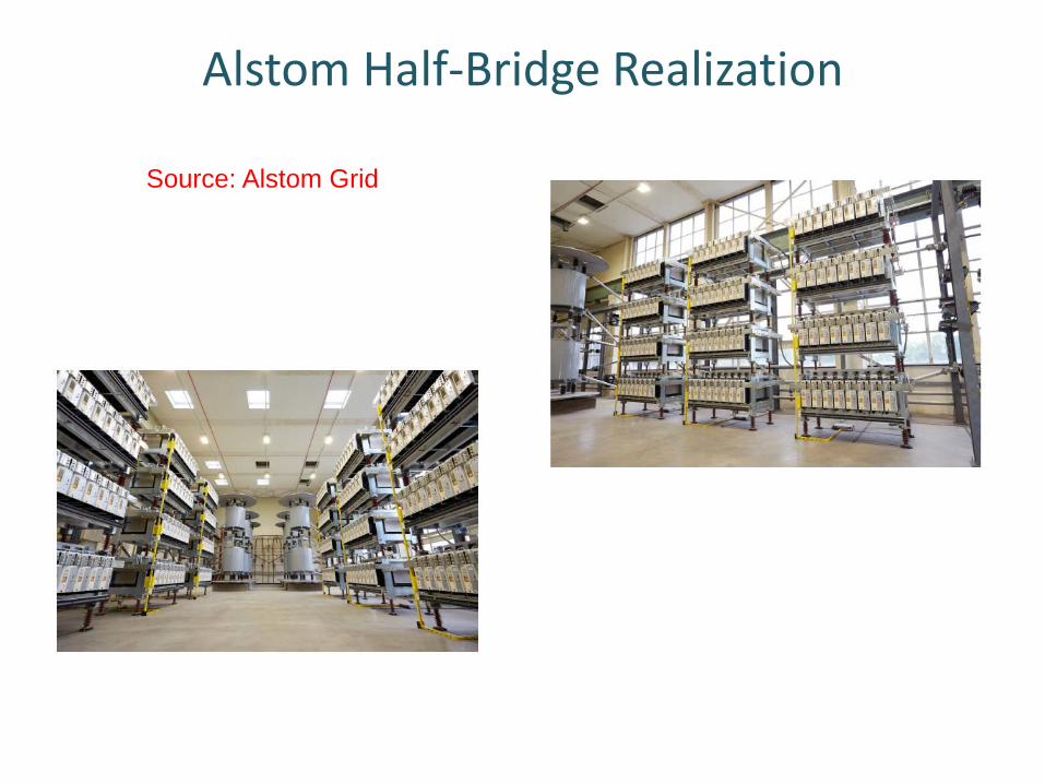
Alstom Half-Bridge Realization
Source: Alstom Grid

Clamped Single-Submodule
• Extension of HB with dc fault blocking • S3, D3, D4 added for dc fault blocking • Normal operation: S1 and S2 switch,
but S3 always ON • S3 => higher losses than HB • S3, D3, D4 only half submodule voltage
lower voltage rating, lower losses • DC fault => S1, S2, S3 OFF and with
pos. curr. D1 and D3 cond, neg. Curr. D2 and D4 cond, different blocking voltage pos. neg
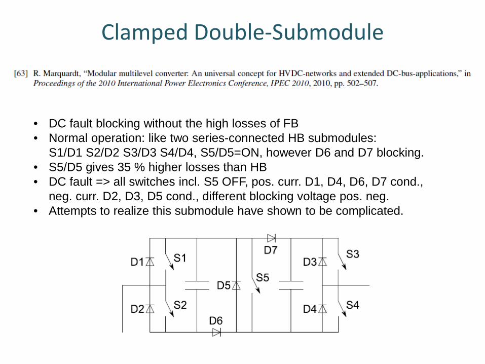
Clamped Double-Submodule
• DC fault blocking without the high losses of FB • Normal operation: like two series-connected HB submodules:
S1/D1 S2/D2 S3/D3 S4/D4, S5/D5=ON, however D6 and D7 blocking. • S5/D5 gives 35 % higher losses than HB • DC fault => all switches incl. S5 OFF, pos. curr. D1, D4, D6, D7 cond.,
neg. curr. D2, D3, D5 cond., different blocking voltage pos. neg. • Attempts to realize this submodule have shown to be complicated.
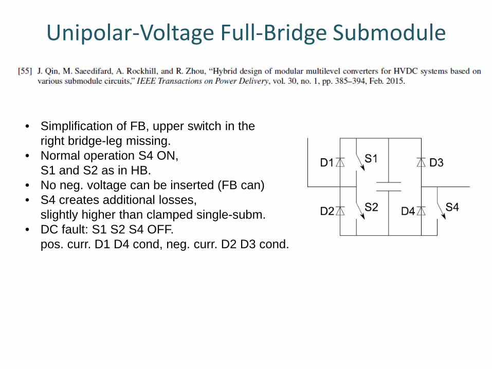
Unipolar-Voltage Full-Bridge Submodule
• Simplification of FB, upper switch in the right bridge-leg missing.
• Normal operation S4 ON, S1 and S2 as in HB.
• No neg. voltage can be inserted (FB can) • S4 creates additional losses,
slightly higher than clamped single-subm. • DC fault: S1 S2 S4 OFF.
pos. curr. D1 D4 cond, neg. curr. D2 D3 cond.
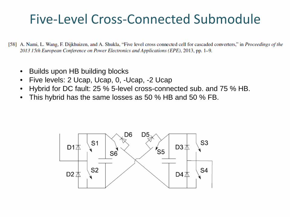
Five-Level Cross-Connected Submodule
• Builds upon HB building blocks • Five levels: 2 Ucap, Ucap, 0, -Ucap, -2 Ucap • Hybrid for DC fault: 25 % 5-level cross-connected sub. and 75 % HB. • This hybrid has the same losses as 50 % HB and 50 % FB.
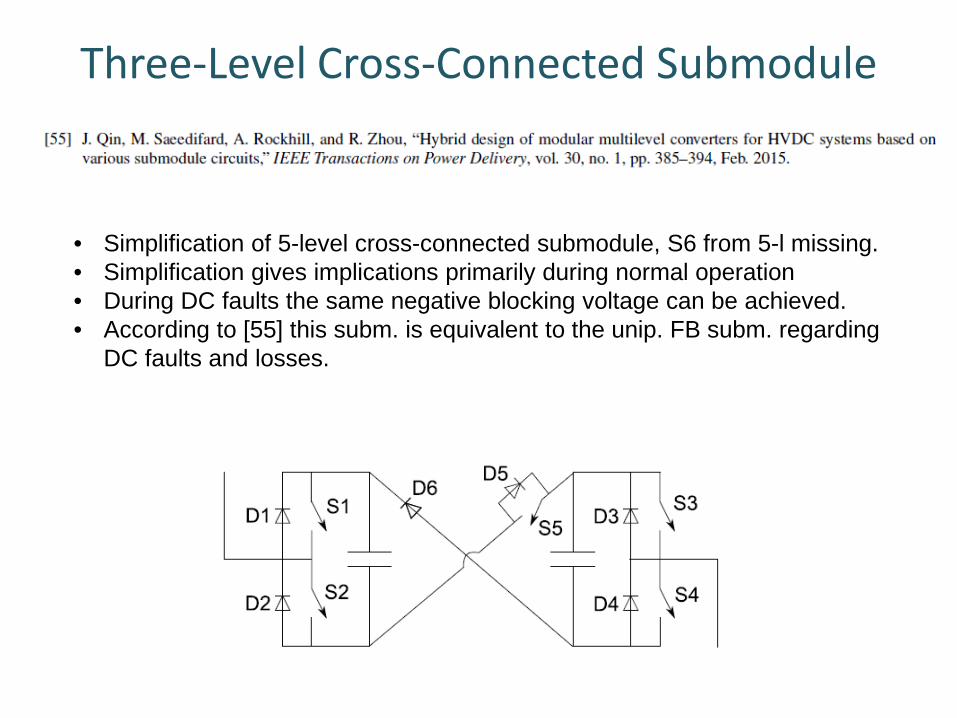
Three-Level Cross-Connected Submodule
• Simplification of 5-level cross-connected submodule, S6 from 5-l missing. • Simplification gives implications primarily during normal operation • During DC faults the same negative blocking voltage can be achieved. • According to [55] this subm. is equivalent to the unip. FB subm. regarding
DC faults and losses.
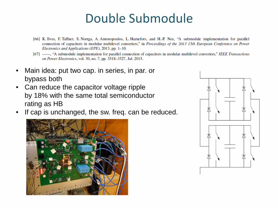
Double Submodule
• Main idea: put two cap. in series, in par. or bypass both
• Can reduce the capacitor voltage ripple by 18% with the same total semiconductor rating as HB
• If cap is unchanged, the sw. freq. can be reduced.
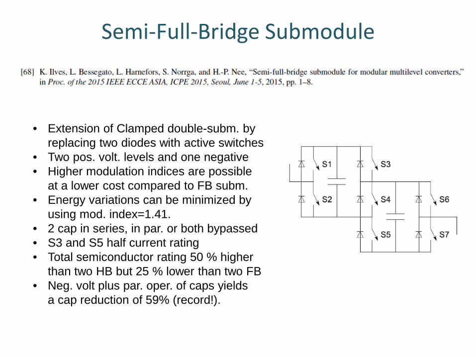
Semi-Full-Bridge Submodule
• Extension of Clamped double-subm. by replacing two diodes with active switches
• Two pos. volt. levels and one negative • Higher modulation indices are possible
at a lower cost compared to FB subm. • Energy variations can be minimized by
using mod. index=1.41. • 2 cap in series, in par. or both bypassed • S3 and S5 half current rating • Total semiconductor rating 50 % higher
than two HB but 25 % lower than two FB • Neg. volt plus par. oper. of caps yields
a cap reduction of 59% (record!).
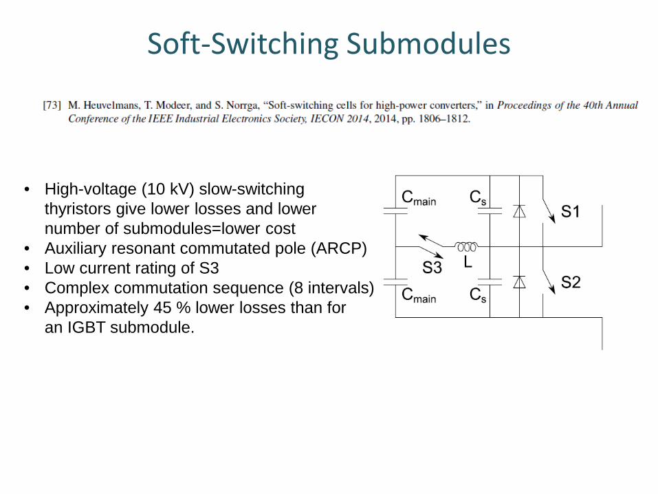
Soft-Switching Submodules
• High-voltage (10 kV) slow-switching thyristors give lower losses and lower number of submodules=lower cost
• Auxiliary resonant commutated pole (ARCP) • Low current rating of S3 • Complex commutation sequence (8 intervals) • Approximately 45 % lower losses than for
an IGBT submodule.

Choice of Main-Circuit Parameters
• Main input data
• Choice of power semiconductor devices
• Choice of the number of submodules
• Choice of the submodule capacitance
• Choice of arm inductance
Main Input Data for Design
• Power transmission need results in choice of XLPE Cable
• Cable voltages: 80, 150, 300 kV, (525 kV)
• Current rating in many steps up to 3 kA, chosen to get sufficient power
• Vd and Id determined from the transmission needs
• AC quantities defined by grid requirements, for instance reactive currents at different voltage levels
• Example grid requirement by ENTSO-E
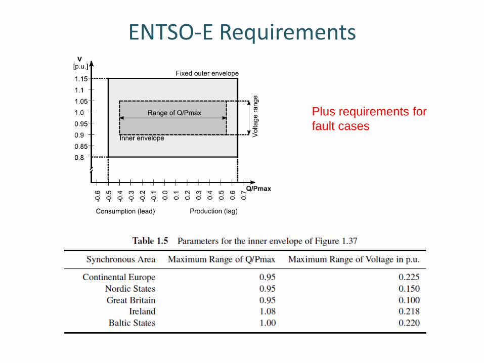
ENTSO-E Requirements
Plus requirements for fault cases
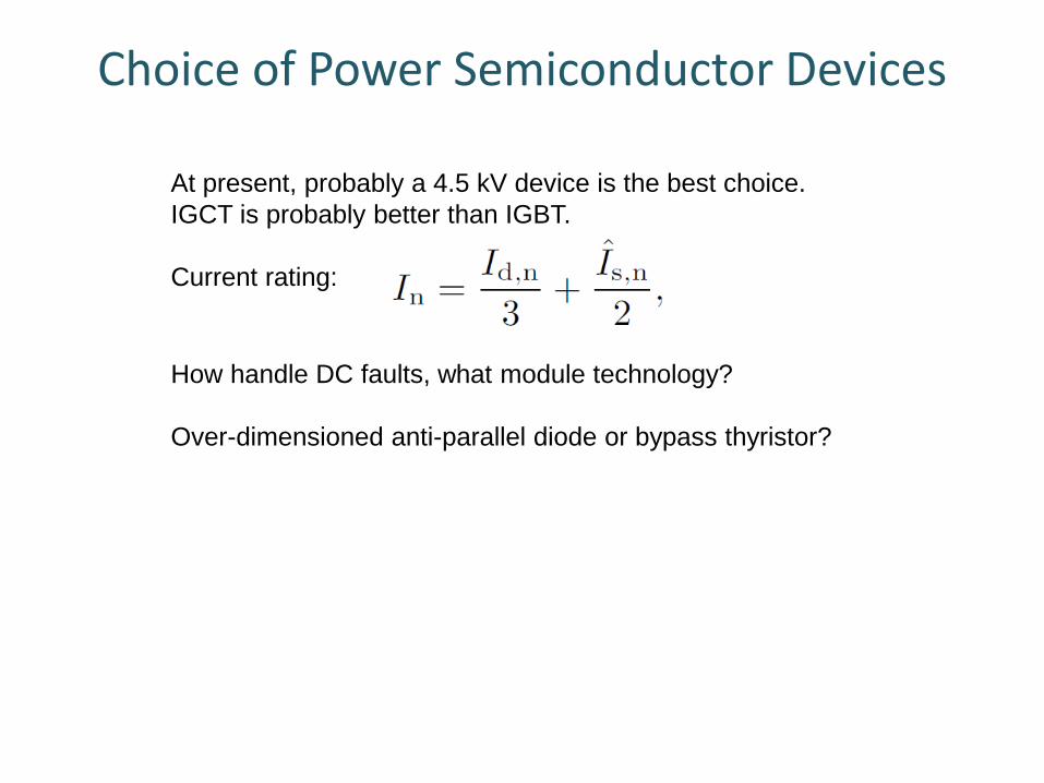
Choice of Power Semiconductor Devices
At present, probably a 4.5 kV device is the best choice. IGCT is probably better than IGBT. Current rating:
How handle DC faults, what module technology? Over-dimensioned anti-parallel diode or bypass thyristor?
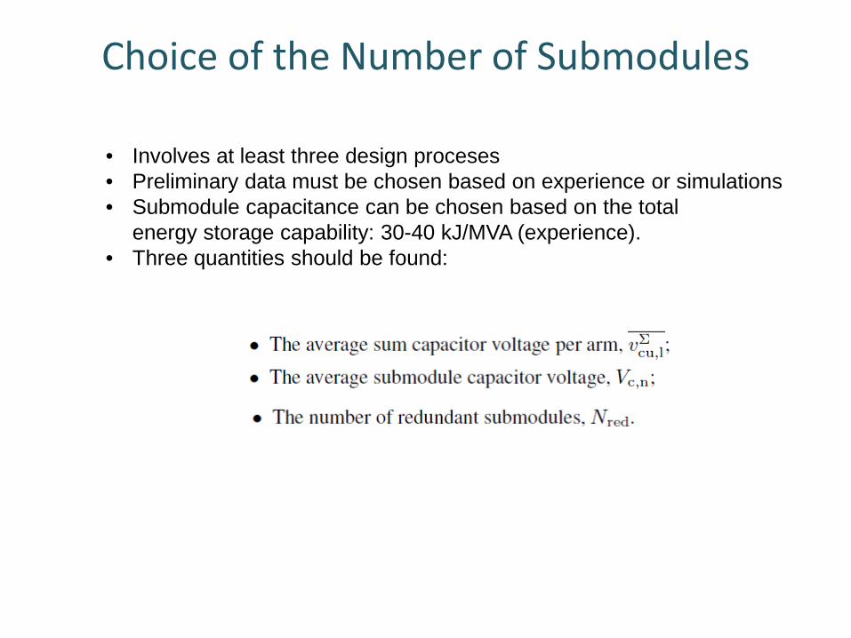
Choice of the Number of Submodules
• Involves at least three design proceses • Preliminary data must be chosen based on experience or simulations • Submodule capacitance can be chosen based on the total
energy storage capability: 30-40 kJ/MVA (experience). • Three quantities should be found:
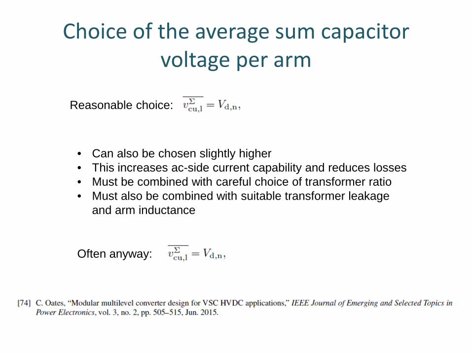
Choice of the average sum capacitor voltage per arm
Reasonable choice:
• Can also be chosen slightly higher • This increases ac-side current capability and reduces losses • Must be combined with careful choice of transformer ratio • Must also be combined with suitable transformer leakage
and arm inductance
Often anyway:
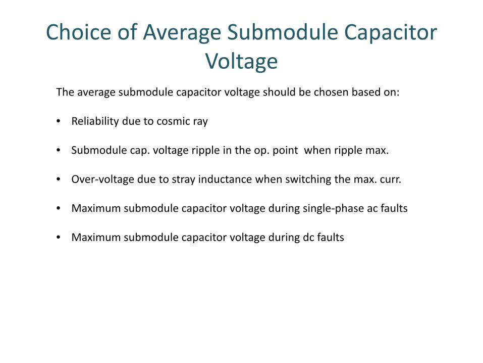
Choice of Average Submodule Capacitor Voltage
The average submodule capacitor voltage should be chosen based on: • Reliability due to cosmic ray
• Submodule cap. voltage ripple in the op. point when ripple max.
• Over-voltage due to stray inductance when switching the max. curr.
• Maximum submodule capacitor voltage during single-phase ac faults
• Maximum submodule capacitor voltage during dc faults
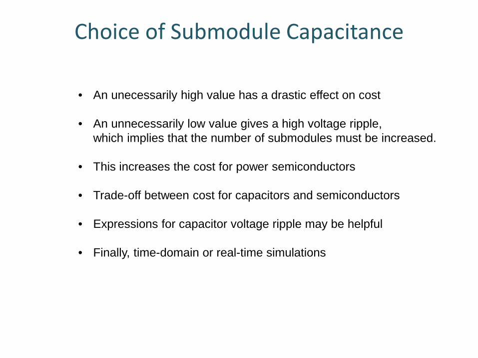
Choice of Submodule Capacitance
• An unecessarily high value has a drastic effect on cost
• An unnecessarily low value gives a high voltage ripple, which implies that the number of submodules must be increased.
• This increases the cost for power semiconductors
• Trade-off between cost for capacitors and semiconductors
• Expressions for capacitor voltage ripple may be helpful
• Finally, time-domain or real-time simulations
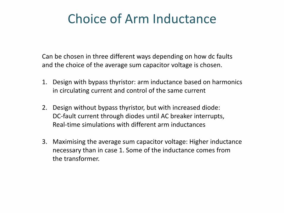
Choice of Arm Inductance
Can be chosen in three different ways depending on how dc faults and the choice of the average sum capacitor voltage is chosen. 1. Design with bypass thyristor: arm inductance based on harmonics
in circulating current and control of the same current
2. Design without bypass thyristor, but with increased diode: DC-fault current through diodes until AC breaker interrupts, Real-time simulations with different arm inductances
3. Maximising the average sum capacitor voltage: Higher inductance necessary than in case 1. Some of the inductance comes from the transformer.

Handling of Redundant and Faulty Submodules
• Several kinds of faults can occur within a submodule • Faulty submodules are bypassed • Bypass: Mechanical vacuum switch (long term) + thyristor for fast
action • When a submodule is bypassed, the remaining submodules get a
higher voltage stress • Number of redundant submodules • Presentation based on:

Two ways of handling redundancy
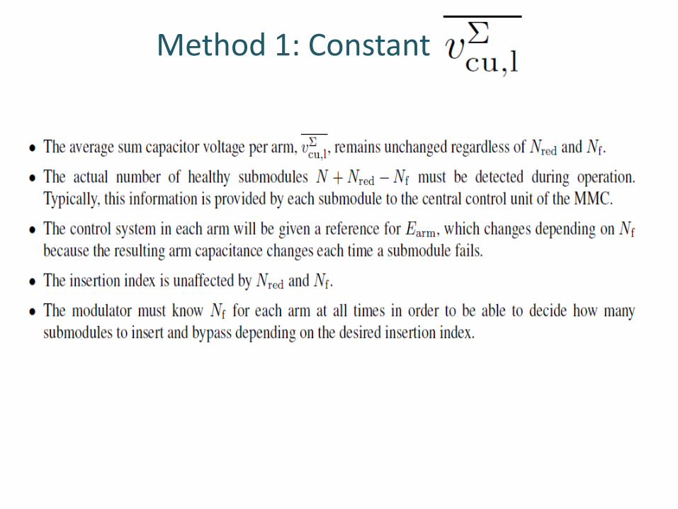
Method 1: Average sum capacitor voltage is kept constant Method 2: The individual average submodule capacitor voltage is kept constant Number of faulty submodules:
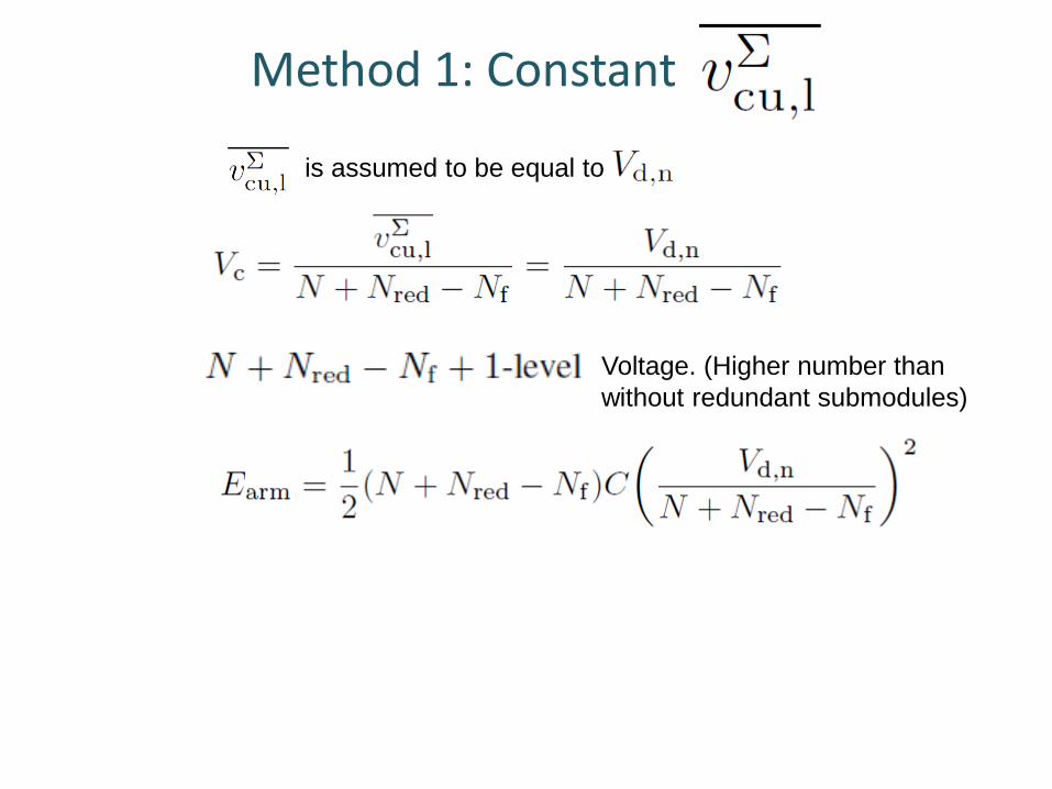
Method 1: Constant
is assumed to be equal to
Voltage. (Higher number than without redundant submodules)
Method 1: Constant
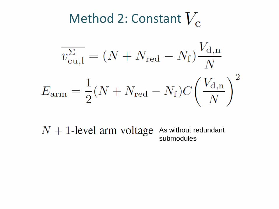
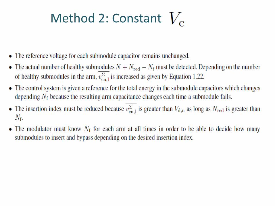
Method 2: Constant
As without redundant submodules
Method 2: Constant
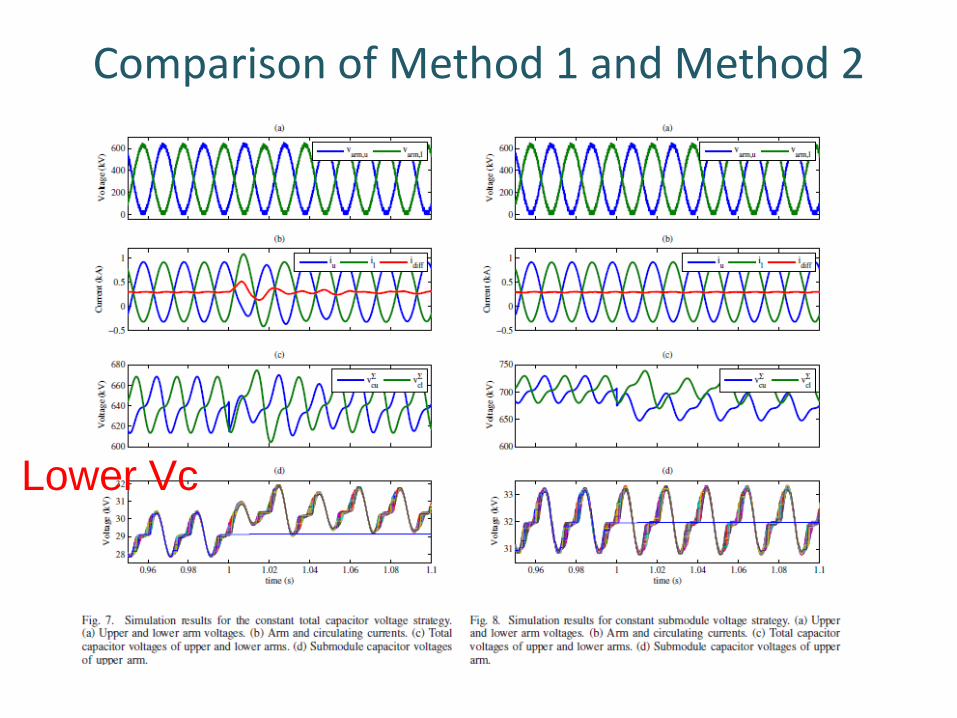
Comparison of Method 1 and Method 2
Lower Vc
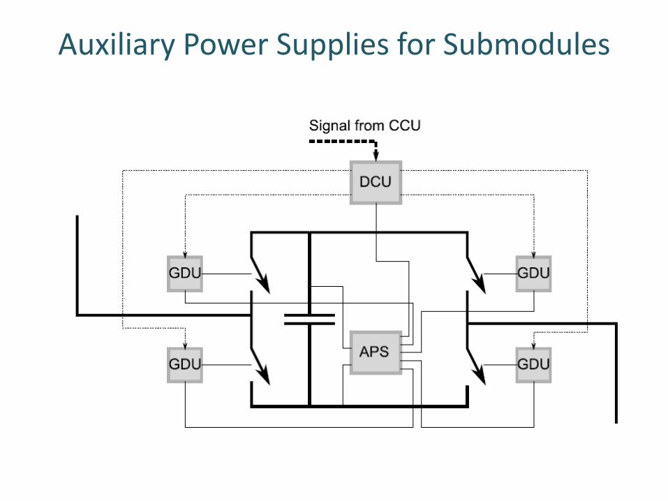
Auxiliary Power Supplies for Submodules
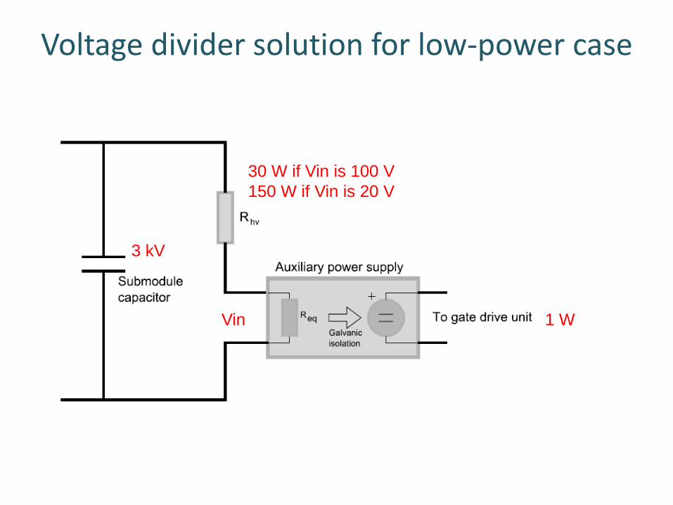
Voltage divider solution for low-power case
30 W if Vin is 100 V 150 W if Vin is 20 V
1 W Vin
3 kV
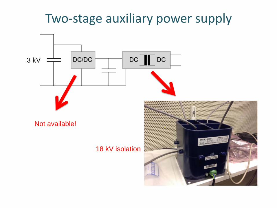
Two-stage auxiliary power supply
18 kV isolation
Not available!
3 kV
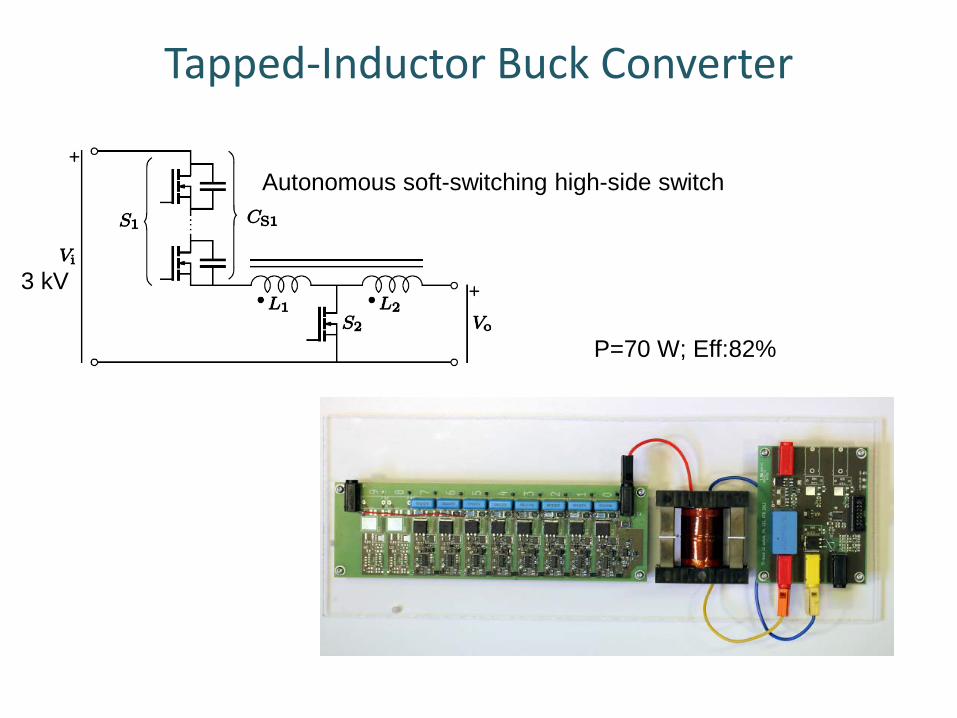
Tapped-Inductor Buck Converter
3 kV
P=70 W; Eff:82%
Autonomous soft-switching high-side switch