Embed Size (px)
Citation preview
DESIGN AND FABRICATION OF A PCB FOR
THE CENTRALIZED CONTROL UNIT OF A
WIRELESS SENSOR NETWORK
B.Tech in Electronics and Communications Engineering
By
PALLABI MISHRA 110EC0173
Under supervision of
Prof. Debiprasad Priyabrata Acharya
Department of Electronics and Communications Engineering
National Institute of Technology, Rourkela

CERTIFICATE
This is to certify that thesis entitled “Design and Fabrication of a PCB for the
Centralized Control Unit of a Wireless Sensor Network” has been completed by
Pallabi Mishra, Roll Number 110EC0173, National Institute of Technology,
Rourkela, India ,during the period July 2013-April 2014 for the Final Year Project
2013-14 under the supervision of Prof. Debiprasad Priyabrata Acharya.
( Prof. Debiprasad Priyabrata Acharya )

ABSTRACT
Wireless Sensor Network stands the advantage of having low power, low cost,
high accuracy and flexible location. In our Project, we aim to design a Printed
Circuit Board which functions as the Centralized Control Unit of a Wireless Sensor
Network that is used to detect flood and transmit the information to the
Registered Mobile Users in the case of a flood. We integrate Audrino Uno and SIM
900 in our PCB. Audrino UNO is the Processor for analyzing data from the
Pressure Sensor Network and predicting the occurrence of a flood. SIM 900
transmits the message of a flood to people in flood-affected region. We use
EAGLE Software to draw the Schematic and Board Diagram of the desired PCB
after removing desired components and adding desired conditions. We use Circuit
CAM to get a Print Out of the PCB.

CONTENTS
1 PREFACE
2 ACKNOWLEDGEMENTS
3 INTRODUCTION
4 FLOOD CONTROL USING ELECTRONICS
5 USE OF PRESSURE SENSORS
6 SCHEMATIC DIAGRAM
7 OUR ALGORITHM
8 DECISION-MAKING
9 PRESSURE SENSOR MPXM2010GS
10 WORKING WITH GSM MODULE

PREFACE
Nowadays Embedded system has captured the field of industry as well
as domestic or practical life of human beings. Glancing at recent
development in the field or electronics and computers, we can just say
that they have captured practically every mode of human’s life and
have given a new way to it. Taking into consideration, the need to save
living beings has inspired us to develop a Disaster Management System
that remotely controls wide range of appliance, in and around the
affected area, with the help of an Embedded System. A Printed Circuit
Board is an extremely compact piece of an Electronic Component that
can simultaneously embed various features and functions. Integrating a
Printed Circuit Board for a Disaster Management system is an excellent
way of ensuring a portable and efficient modeule with desired
functions even in remote areas.
Finally we feel very much satisfied in presenting this project, which
would be of great use to our society.

ACKNOWLEDGEMENTS
We are extremely grateful to our project guide, Prof. D.P. Acharya for his
insightful suggestions on the project work and for guiding us during the project
with her encouragement, support and cooperation. We would like to convey our
sincerest gratitude and indebtedness to all our faculty members and staffs of
Department of Electronics and Communications Engineering, NIT Rourkela, who
showed their great efforts and guidance during required times without which it
would have been very difficult to carry out our project work. Moreover, an
assemblage of this nature could never have been attempted with our reference to
the works of others. We acknowledge our indebtedness to all of them. Finally, we
would also like to extend our heart- felt thanks to our family for their moral
support, love and affection.

INTRODUCTION
The disaster management area is described by: appropriated control;
vulnerability, uncertainty, imprecision and inclination; different stakeholders with
diverse points and destinations; and restricted assets which consistently
fluctuate. A disaster management framework is seen as being made out of self-
sufficient, sensitive and proactive executors that can sense, act and interface so
as to attain singular and aggregate points. These operators need to have the
capacity to make the best utilization of accessible data, be adaptable and
coordinated in their choice making, cognisant of the way that there are different
executors, and versatile to their nature's turf. This obliges a multi-disciplinary
methodology, specifically:
• Filtering and data fusion methods for estimating relevant state variables,
such as the position of rescue vehicles and wounded civilians
• Decision-making and machine learning methods for determining actions in
response to states, such as when and where to route a particular rescue
vehicle
• Multi-agent systems, game theory, and mechanism design methods to
manage the interaction between multiple actors and to model collective
behaviour
• System architecture studies of different agent organisations and information
exchange topologies, for example centralised, hierarchical or decentralised
systems
The test is to coordinate these components so as to create decentralized
information and data frameworks that can work viably in exceedingly unverifiable
and dynamic situations. This is not only an exploration move; it is a key
prerequisite for some mechanical and business associations, exemplified by the
disaster management requisition area.
FLOOD CONTROL USING ELECTRONICS
Two early types of flood detection and warning systems have been established:
A) Non-WSN and B) WSN
A) Non-WSN Systems:
These frameworks have a primitive strategy of surge identification obliging
prepared faculty. It includes generally manual methods and subsequently is
unmanageable. Here, the dependability of the whole component relies on the
expertise and knowledge of the staff utilized and is hence restricted by their
velocity and spryness. Late improvements have prompted mechanized telemetry
frameworks. Indeed these are exorbitant as they require occasional
establishment of repeaters and transmitters. The vast majority of the telemetric
frameworks take after a brought together computational procedure. Likewise
sending of an extensive number of telemetric frameworks to blanket the whole
locale gets unrealistic because of the substantial costs included. Disregarding
having these issues, the non-WSN frameworks are working in numerous nations
on the planet.
B) WSN Systems:
WSNs could be characterized as low power, minimal effort, multi-jumping
frameworks that are free of outer administration suppliers, can structure an
extendable system without viewable pathway scope; however have recovering
toward oneself information ways. WSNs could be sent pretty much
homogeneously in a land locale utilizing a two-layered methodology having
bunches of short separation corresponding hubs together with a few hubs
equipped for correspondence over a more extensive reach. WSN hubs correspond
just with neighboring hubs to decrease the transmission force and misfortunes,
consequently taking out the requirement for unreasonable repeaters and
transmitters utilized as a part of conventional telemetry frameworks. Each hub in
a WSN can go about as an information obtaining gadget, an information switch
and an information aggregator. This construction modeling expands the repetition
and therefore the unwavering quality of the whole blaze- surge checking
framework. The autonomy from outsider suppliers and the nonattendance of
framework prerequisites – as those required in cell based telemetry frameworks

permit a WSN to be conveyed rapidly. They permit on the web, change toward
oneself of the forecast mode
Three types of models may be designed:
A) Centralized, B) Distributed or C) Hybrid
A) Centralized Model: A centralized model is one where calculation happens at the central node just. It
needs less number of segments as terminal hubs needn't bother with the
electronic parts needed for computational purposes. Nonetheless, the entire
framework fizzles if the central node comes up short regardless of the fact that it
is just a solitary purpose of disappointment (accepting a completely joined
reinforcement of the focal hub is truant). There is additionally a need to stay away
from bottlenecks because of transmission of measured information all the while
from all the sensing nodes, which can restrict the information accessible to the
model to use for alignment and expectation therefore constraining the
adaptability of the model.
B) Distributed Model: A distributed model is unified with processings at a few levels rather than stand
out registering hub as in the past model. A large portion of the weaknesses of a
centralized framework are tended to in this model as diverse terminal sensors act
together to give the gathered information to scaffold hubs, distinguish inside
disappointments and to adjust to changes in topology. This model likewise
expands the dependability of a framework by presenting repetition as the same
counts are carried out at diverse hubs and afterward matched. Nonetheless, they
experience the ill effects of the trouble and expense of upkeep of various sensors
with extra functionalities and likewise in guaranteeing fitting correspondence
around these heterogeneous sensors.

C) Hybrid Model: As the name recommends, this model embodies some piece of the centralized
model and some piece of the distributed model. The degree to which a piece of
each one model (centralized or distributive) is incorporated in it is adaptable and
may shift according to framework prerequisites. This model means to halfway
consolidate the points of interest of both the above frameworks and at the same
time, countervail the inconveniences of either framework by joining both. Despite
the fact that the system progression continues as before here as in the past cases,
processing is carried out on numerous hubs not at all like the centralized strategy,
but calculation in just about all hubs is not done as in the distributed technique. In
this manner, it is conceivable to achieve a suitable parity of the expense of
organization and the repetition and unwavering quality of the framework as
required.
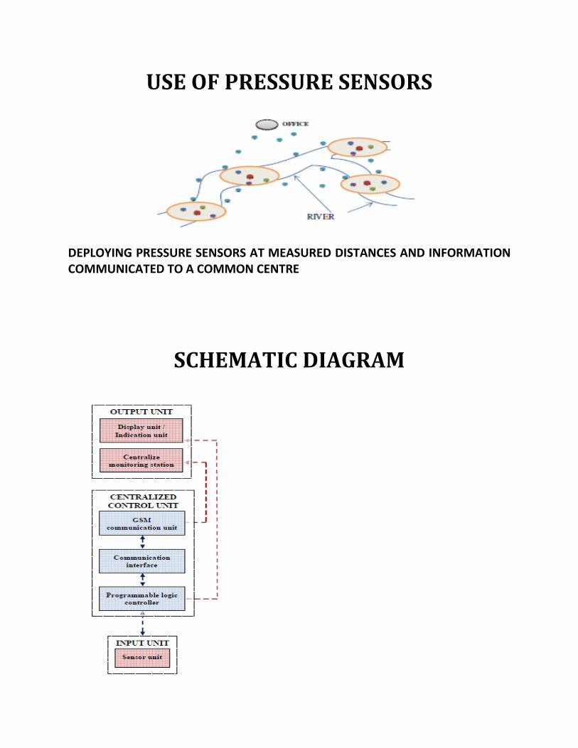
USE OF PRESSURE SENSORS
DEPLOYING PRESSURE SENSORS AT MEASURED DISTANCES AND INFORMATION
COMMUNICATED TO A COMMON CENTRE
SCHEMATIC DIAGRAM

PRESSURE SENSOR MPXM2010GS
The measurement technique uses the air pressure in a closed tube above a
column of water to determine the water level. The following diagram shows the
basic components of the measuring system. As the water level in the column
changes, the air pressure in the closed tube above the column will change
proportionally. By measuring the air pressure, the water level can be determined.

PRINTED CIRCUIT BOARD
A printed circuit board (PCB) mechanically supports and electrically connects
electronic segments utilizing conductive tracks, cushions and different
characteristics carved from copper sheets overlaid onto a non-conductive
substrate. PCBs might be single sided (one copper layer), twofold sided (two
copper layers) or multi-layer. Conductors on distinctive layers are joined with
plated-through gaps called vias. Propelled PCBs may hold segments - capacitors,
resistors or dynamic gadgets - implanted in the substrate.
Printed circuit sheets are utilized as a part of everything except the most
straightforward electronic items. Alternatives to PCBs incorporate wire wrap and
point-to-point development. PCBs require the extra plan exertion to lay out the
circuit yet assembling and get together could be computerized. Assembling
circuits with PCBs is less expensive and speedier than with other wiring strategies
as part are mounted and set up with one single part. Moreover, driver wiring
lapses are wiped out.
At the point when the board has just copper associations and no inserted
segments it is all the more accurately called a printed wiring board (PWB) or
scratched wiring board. Despite the fact that more exact, the term printed wiring
board has fallen into neglect. A PCB populated with electronic segments is known
as a printed circuit get together (PCA), printed circuit board gathering or PCB
gathering (PCBA). The IPC favored term for gathered prepares to leave is circuit
card gathering (CCA), for amassed backplanes it is backplane gatherings. The term
PCB is utilized casually both for exposed and collected sheets.
The world business sector for uncovered PCBs arrived at almost $60 billion in
2012.
DESIGN
Printed circuit board artwork generation was at first a completely manual
procedure done on clear mylar sheets at a scale of normally 2 or 4 times the
coveted size. The schematic chart was initially changed over into a design of

segments pin cushions, then follow were steered to give the obliged
interconnections. Preprinted non-imitating mylar networks supported in format,
and rub-on dry exchanges of basic courses of action of circuit components
(cushions, contact fingers, incorporated circuit profiles, et cetera) helped
institutionalize the design. Follow between gadgets were made with sticky toward
oneself tape. The completed format "artwork" was then photographically
recreated on the oppose layers of the spotless covered copper-clad sheets.
Current practice is less work-serious since machines can consequently perform a
number of the format steps. The general movement for a business printed circuit
board configuration might include:
1. Schematic capture through an electronic configuration automation device.
2. Card measurements and format are chosen focused around obliged
hardware and instance of the PCB. Focus the altered segments and heat sinks if
needed.
3. 1 to 12 layers or all the more relying upon design complexity. Ground plane
and force plane are chosen. Signal planes where indicators are directed are in top
layer and also inside layers.
4. Line impedance determination utilizing dielectric layer thickness, steering
copper thickness and follow-width. Trace separation likewise considered if there
should arise an occurrence of differential indicators. Microstrip, stripline or
double stripline might be utilized to course indicates.
5. Placement of the segments. Thermal considerations and geometry are
considered. Vias and lands are checked.
6. Routing the signal traces. For ideal EMI performance high frequency signals
are steered in interior layers between power or ground planes as power planes
carry on as ground for AC.
7. Gerber file generation for assembling.

In the outline of the PCB craftsmanship, a force plane is the partner to the ground
plane and carries on as an AC sign ground, while giving DC voltage to controlling
circuits mounted on the PCB. In electronic configuration computerization (EDA)
outline devices, force planes (and ground planes) are normally drawn naturally as
a negative layer, with clearances or associations with the plane made
consequently.
MANUFACTURING
PCB assembling comprises of numerous steps.
PCB Cam
Producers never utilize the Gerber or Excellon files straightforwardly on their
supplies, however dependably read them into their CAM framework. PCB's can't
be produced professionally without a CAM framework. The PCB CAM framework
performs the accompanying functions:
1. Information of the Gerber information
2. Confirm the information; alternatively DFM
3. Make up for deviations in the assembling courses of action (e.g. scaling to
make up for twists throughout overlay)
4. Panelize
5. Yield of the computerized instruments (layer pictures, drill files, AOI
information, electrical test files,.)
Panelization
Panelization is a methodology used to handle PCBs which might overall be so little
it is not possible procedure. Various indistinguishable circuits are printed onto a
bigger board (the board) which can then be taken care of in the typical way. The
board is broken separated into unique PCBs when all other preparing is finished.
Dividing the distinct PCBs is much of the time supported by boring or steering
punctures along the limits of the distinctive circuits, much like a sheet of postage
stamps. An alternate technique, which consumes less room, is to cut V-formed
scores over the full measurement of the board. The distinct PCBs can then be
broken separated along this line of weakness.
The procedure of evacuating distinctive PCBs from a bigger board is called
Depaneling. While penetrated/steered punctures and furrows were normal for
various years, today this is regularly done by lasers, which cut the board with no
contact. This diminishes the burdens on the delicate circuits brought on by
torque. This system is regularly totally robotized with full loads up entering the
laser depaneling machine by means of transport, being cut into distinctive pieces
by laser, and leaving the framework through transport, and here and there
stacked, on the other side.
Copper patterning
The pattern in the producer's PCB CAM framework is generally yield on a
photomask (photo-tool, film) by a photoplotter and repeated by means of silk
screen printing or by uncovering on a photograph-delicate photoresist covering.
Immediate imaging methods are at times utilized for high-resolution
prerequisites.
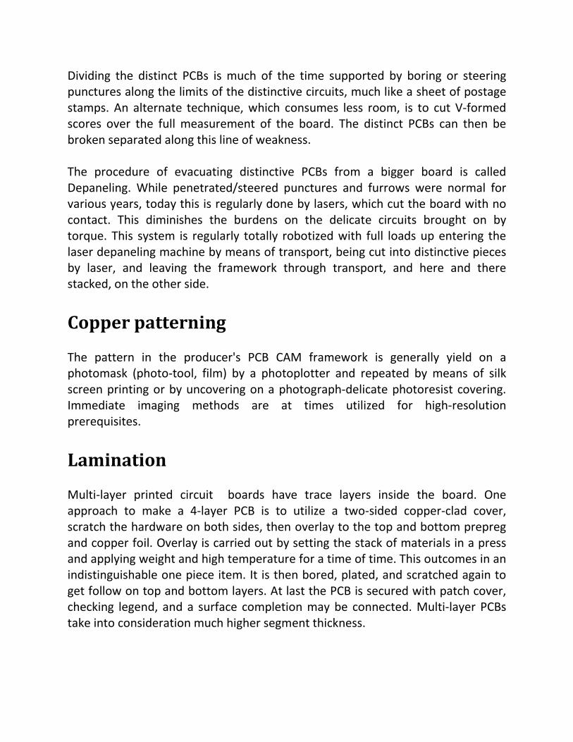
Lamination
Multi-layer printed circuit boards have trace layers inside the board. One
approach to make a 4-layer PCB is to utilize a two-sided copper-clad cover,
scratch the hardware on both sides, then overlay to the top and bottom prepreg
and copper foil. Overlay is carried out by setting the stack of materials in a press
and applying weight and high temperature for a time of time. This outcomes in an
indistinguishable one piece item. It is then bored, plated, and scratched again to
get follow on top and bottom layers. At last the PCB is secured with patch cover,
checking legend, and a surface completion may be connected. Multi-layer PCBs
take into consideration much higher segment thickness.

WHAT OUR PCB CONTAINS
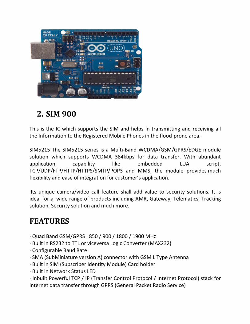
1. ARDUINO UNO
It functions as the processor for aquiring data from the Pressure Sensors,
processing them for predicting floods, storing the desired data and transmitting
the Flood Alarms.
Arduino is a single-board microcontroller, proposed to make the requisition of
intuitive questions or situations more accessible. The hardware comprises of an
open-source hardware board composed around a 8-bit Atmel AVR
microcontroller, or a 32-bit Atmel ARM. Current models offer a USB interface, 6
simple information pins, and 14 computerized I/O pins which permits the client to
join different expansion sheets.
Presented in 2005, it was intended to give understudies a cheap and simple
approach to program intuitive items. It accompanies a straightforward
coordinated the earth (IDE) that runs on customary Pcs and permits to compose
programs for Arduino utilizing C or C++.
An Arduino board comprises of an Atmel 8-bit AVR microcontroller with
correlative segments to encourage programming and joining into different
circuits. A vital part of the Arduino is the standard way that connectors are
uncovered, permitting the CPU board to be associated with a mixture of
compatible extra-modules known as shields. A few shields speak with the Arduino
board straightforwardly over different pins, yet numerous shields are exclusively
addressable by means of an I²c serial transport, permitting numerous shields to
be stacked and utilized within parallel. Official Arduinos have utilized the megaavr
arrangement of chips, particularly the Atmega8, Atmega168, Atmega328,
Atmega1280, and Atmega2560. A handful of different processors have been
utilized by Arduino compatibles. Most sheets incorporate a 5 volt straight
controller and a 16 Mhz precious stone oscillator (or ceramic resonator in a few
variants), in spite of the fact that a few outlines, for example, the Lilypad run at 8
Mhz and forgo the locally available voltage controller because of particular
structure-element limitations. An Arduino's microcontroller is likewise
prearranged with a boot loader that rearranges transferring of projects to the on-

chip streak memory, contrasted and different gadgets that normally require an
outer software engineer. This makes utilizing an Arduino more direct by
permitting the utilization of a normal machine as the software engineer.
The Arduino board uncovered the majority of the microcontroller's I/O pins for
utilization by different circuits. The Diecimila, Duemilanove, and current Uno give
14 computerized I/O sticks, six of which can generate beat-width balanced signs,
and six simple inputs. These pins are on the highest point of the board, by means
of female 0.10-inch (2.5 mm) headers. A few module-requisition shields are
likewise financially accessible.
SCHEMATIC DIAGRAM

IMPORTANT ICS
ATMEGA8
ATMEGA8U2-MU
2. SIM 900
This is the IC which supports the SIM and helps in transmitting and receiving all
the Information to the Registered Mobile Phones in the flood-prone area.
SIM5215 The SIM5215 series is a Multi-Band WCDMA/GSM/GPRS/EDGE module
solution which supports WCDMA 384kbps for data transfer. With abundant
application capability like embedded LUA script,
TCP/UDP/FTP/HTTP/HTTPS/SMTP/POP3 and MMS, the module provides much
flexibility and ease of integration for customer’s application.
Its unique camera/video call feature shall add value to security solutions. It is
ideal for a wide range of products including AMR, Gateway, Telematics, Tracking
solution, Security solution and much more.
FEATURES
· Quad Band GSM/GPRS : 850 / 900 / 1800 / 1900 MHz
· Built in RS232 to TTL or viceversa Logic Converter (MAX232)
· Configurable Baud Rate
· SMA (SubMiniature version A) connector with GSM L Type Antenna
· Built in SIM (Subscriber Identity Module) Card holder
· Built in Network Status LED
· Inbuilt Powerful TCP / IP (Transfer Control Protocol / Internet Protocol) stack for
internet data transfer through GPRS (General Packet Radio Service)
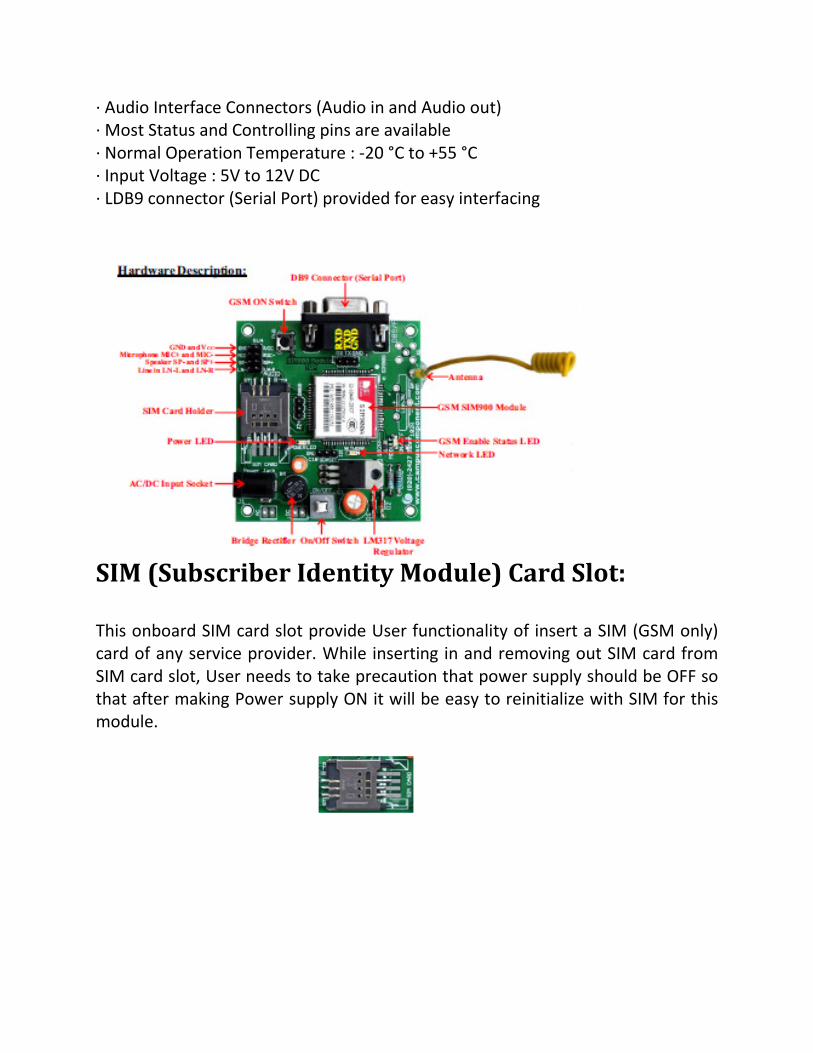
· Audio Interface Connectors (Audio in and Audio out)
· Most Status and Controlling pins are available
· Normal Operation Temperature : -20 °C to +55 °C
· Input Voltage : 5V to 12V DC
· LDB9 connector (Serial Port) provided for easy interfacing
SIM (Subscriber Identity Module) Card Slot:
This onboard SIM card slot provide User functionality of insert a SIM (GSM only)
card of any service provider. While inserting in and removing out SIM card from
SIM card slot, User needs to take precaution that power supply should be OFF so
that after making Power supply ON it will be easy to reinitialize with SIM for this
module.
SCHEMATIC DIAGRAM
REMOVING THE REDUNTANT
COMPONENTS
Now, we move on to remove the reduntant designs in the PCB. There are certain
components which are just for testing the functionality of various parts or
checking the consistency which we are removing here for the puprpose of making
a Compact PCB.
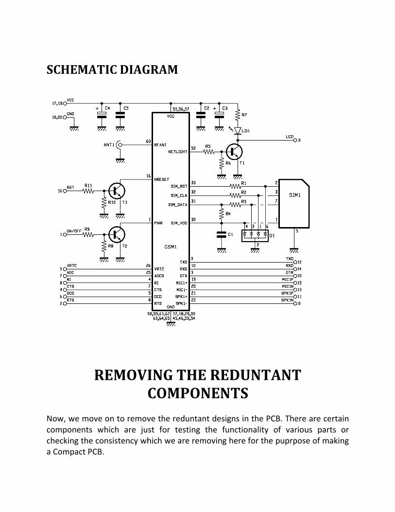
SCHEMATIC DIAGRAM
REMOVING THE REDUNTANT
COMPONENTS
Now, we move on to remove the reduntant designs in the PCB. There are certain
components which are just for testing the functionality of various parts or
checking the consistency which we are removing here for the puprpose of making
REMOVING THE REDUNTANT
Now, we move on to remove the reduntant designs in the PCB. There are certain
components which are just for testing the functionality of various parts or
checking the consistency which we are removing here for the puprpose of making

At this stage, we remove the individual redundant components from each
Component individually. In the net stage, we are going to merge both of them.
ARDUINO UNO
The above diagram shows components or connections which are not used in
Arduino UNO Board.
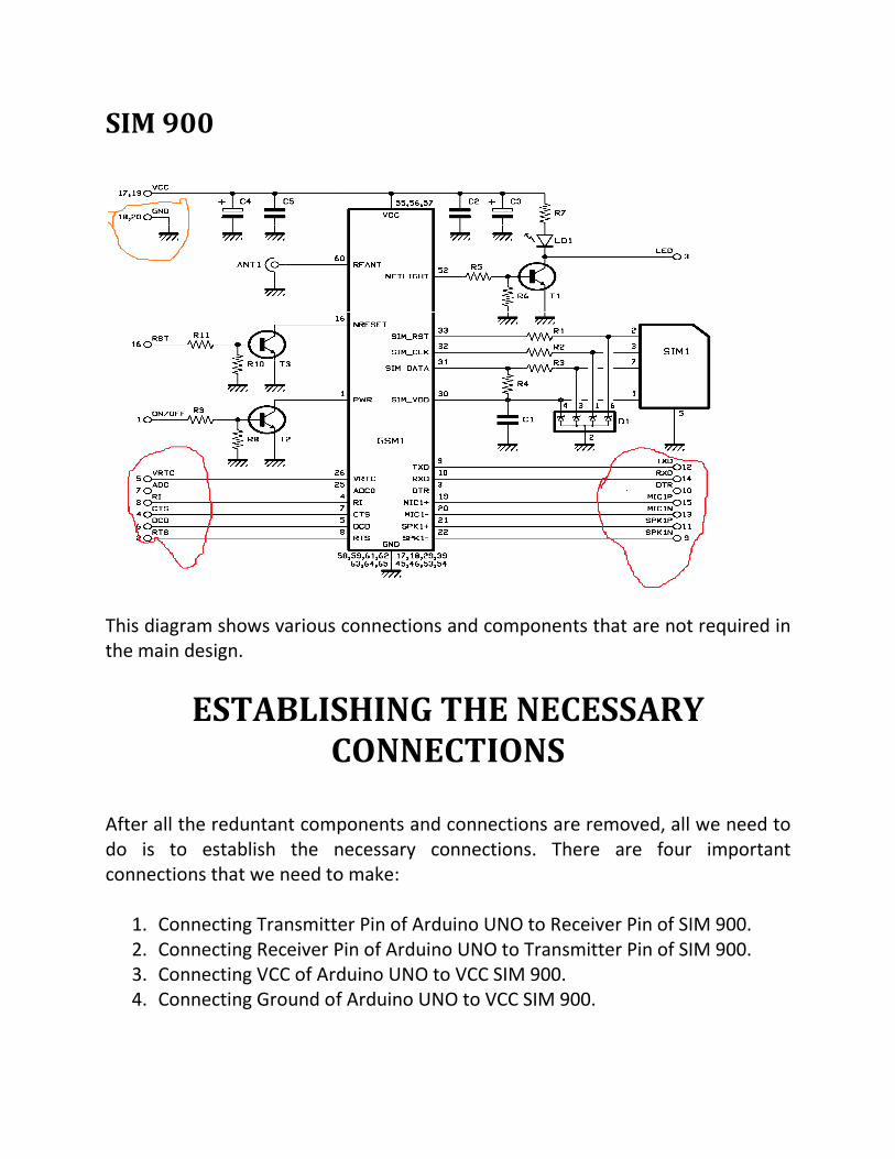
SIM 900
This diagram shows various connections and components that are not required in
the main design.
ESTABLISHING THE NECESSARY
CONNECTIONS
After all the reduntant components and connections are removed, all we need to
do is to establish the necessary connections. There are four important
connections that we need to make:
1. Connecting Transmitter Pin of Arduino UNO to Receiver Pin of S
2. Connecting Receiver Pin of Arduino UNO to
3. Connecting VCC of Arduino UNO to
4. Connecting Ground of Arduino UNO to
This diagram shows various connections and components that are not required in
ESTABLISHING THE NECESSARY
CONNECTIONS
After all the reduntant components and connections are removed, all we need to
do is to establish the necessary connections. There are four important
connections that we need to make:
Connecting Transmitter Pin of Arduino UNO to Receiver Pin of S
Pin of Arduino UNO to Transmitter Pin of S
of Arduino UNO to VCC SIM 900.
of Arduino UNO to VCC SIM 900.
This diagram shows various connections and components that are not required in
ESTABLISHING THE NECESSARY
After all the reduntant components and connections are removed, all we need to
do is to establish the necessary connections. There are four important
Connecting Transmitter Pin of Arduino UNO to Receiver Pin of SIM 900.
Pin of SIM 900.
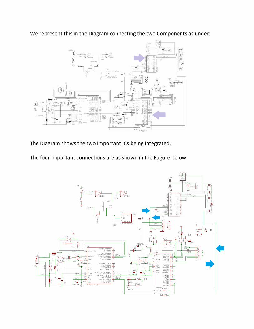
We represent this in the Diagram connecting the two Components as under:
The Diagram shows the two important ICs being integrated.
The four important connections are a
We represent this in the Diagram connecting the two Components as under:
The Diagram shows the two important ICs being integrated.
The four important connections are as shown in the Fugure below:
We represent this in the Diagram connecting the two Components as under:
SOFTWARES USED
1. EAGLE Software
2. Circuit CAM Software
EAGLE IMPLEMENTATION
A BIT ABOUT EAGLE
EAGLE (Easily Applicable Graphical Layout Editor,German: Einfach Anzuwendende
r Grafischer Layout-Editor) by CadSoft Computer is a flexible, expandable and
scriptable EDA application with schematic capture editor, PCB layout editor, auto-
router and CAM and BOM tools developed by CadSoft Computer GmbH, Germany
since 1988.
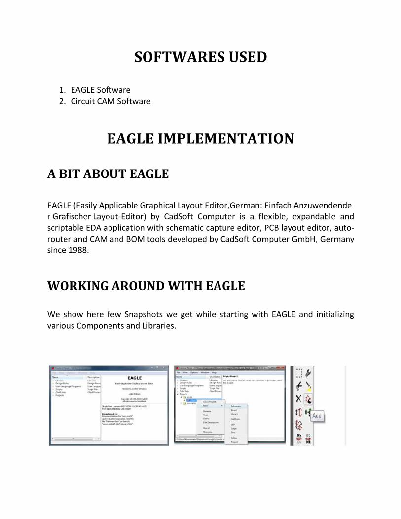
WORKING AROUND WITH EAGLE
We show here few Snapshots we get while starting with EAGLE and initializing
various Components and Libraries.

MOVING ON WITH OUR PROJECT
Shown below is the Final PCB Schematic Diagram that we need to implement in
Hardware:
OVING ON WITH OUR PROJECT
Shown below is the Final PCB Schematic Diagram that we need to implement in
Shown below is the Final PCB Schematic Diagram that we need to implement in
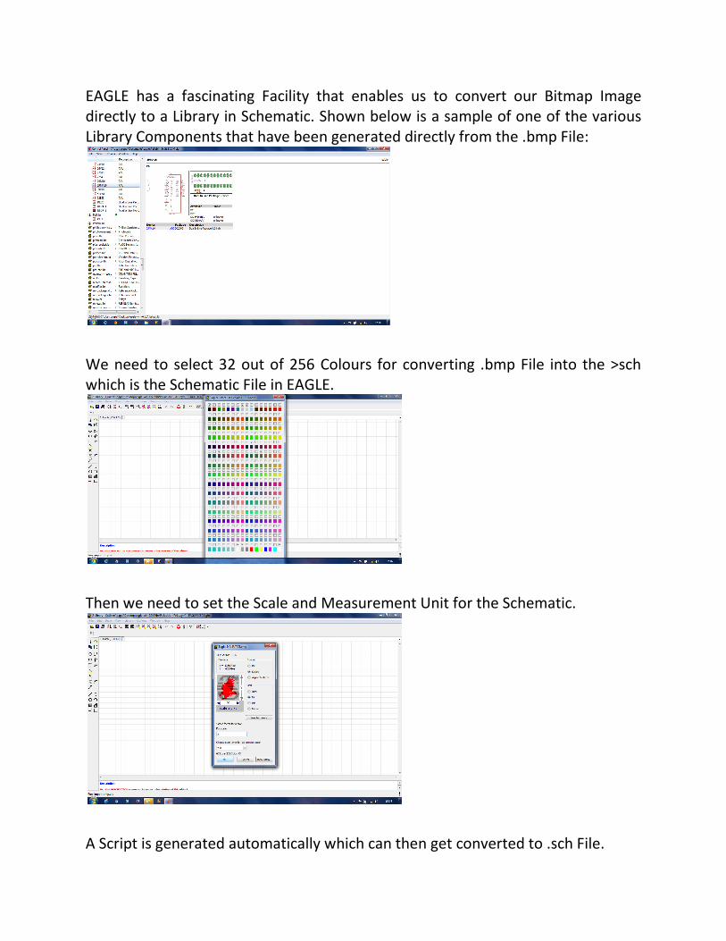
EAGLE has a fascinating Facility that enables us to convert our Bitmap Image
directly to a Library in Schematic. Shown below is a sample of one of the various
Library Components that have been generated directly from the .bmp File:
We need to select 32 out of 256 Colours for converting .bmp File into the >sch
which is the Schematic File in EAGLE.
Then we need to set the Scale and Measurement Unit for the Schematic.
A Script is generated automatically which can then get converted to .sch File.

Shown below is a Snapshot of the screen when the Schematic File is generated
from the Script.
For Conversion into a CAM File for further processing with CAM, similarly we need
to get the Board File of our Project which is a .brd File.
Then, we need to define seven attributes, namely Component, Solder,
Component Silk, Solder Silk, Component End, Solder End and Drill as shown
below:
Finally our CAM File is ready for further processing in the Circuit CAM Software.
CIRCUIT CAM IMPLEMENTATION
A BIT ABOUT CIRCUIT CAM
CircuitCAM is a Computer Aided Manufacturing (CAM) system for Printed Circuit
Boards (PCB) and other related technologies from LKSoft. It is supporting
technologies for both prototyping and line production. The supported
manufacturing processes we are using here are:-
• Data preparation for photo-plotter.
• Conventional milling and drilling (contour routing) including optimization of
tool-paths.
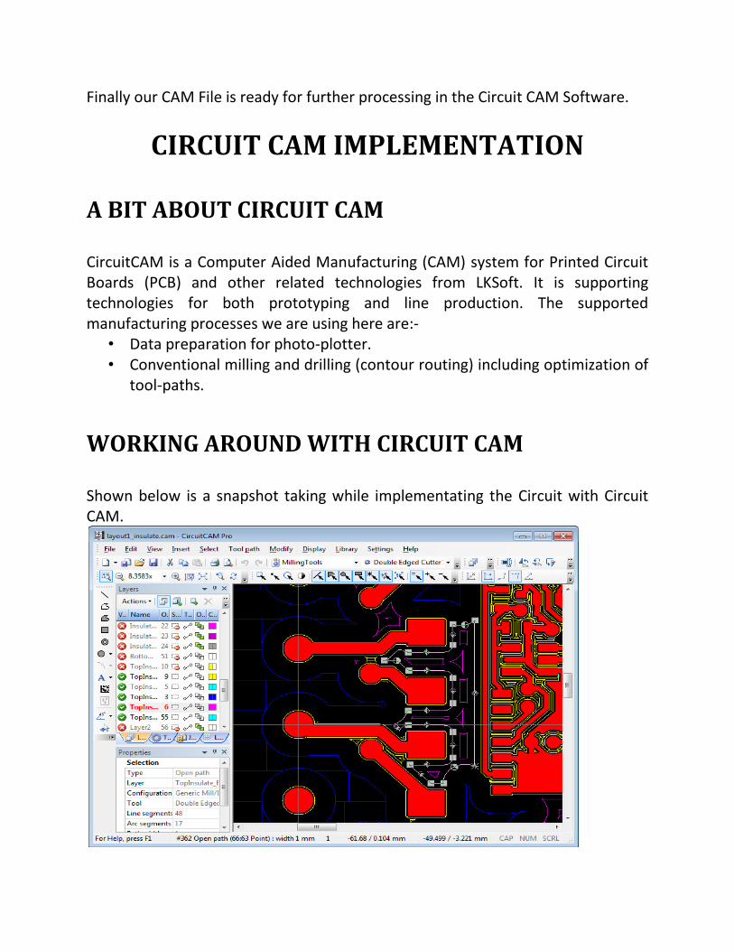
WORKING AROUND WITH CIRCUIT CAM
Shown below is a snapshot taking while implementating the Circuit with Circuit
CAM.

CONCLUSION
After proper implementation in EAGLE Software as well as Circuit CAM Software,
we have a .cam File which can be printed to get our Final Printed Circuit Board
which embeds all our desired characterstics as well as is portable and efficient to
serve as the Centralized Control Unit of a Wireless Sensor Network and can be
used in remote areas for prediction of flood as well as passing on Alert Messages
about the occurrence of a flood to the Registered Mobile Numbers.
Further testing on the Printed Circuit Board using Code and the Pressure Sensor
Network may show us areas where we need to improve and customize so as to
make our PCB better and efficient.

SOURCES AND CITATIONS
1. http://www.airborn.com.au/layout/pcbtut.html
2. http://www.smps.us/layout.html
3. http://www.wikipedia.com
4. http://scholar.google.com