Embed Size (px)
Citation preview
1
DESIGN ANALYSIS OF PLL COMPONENTS
A THESIS SUBMITTED IN PARTIAL FULFILLMENT OF THE
REQUIREMENTS FOR THE DEGREE OF
Bachelor of technology
In
Electronics &Instrumentation Engineering
By
Ranjit Dash Roll no: 10607017
&
Dipankar Ghosh Roll No: 10607015
Under the guidance of
Prof. Debiprasad Priyabrata Acharya
Department of Electronics & Communication Engineering
National Institute of Technology Rourkela, 2010
2
Electronics & Communication Department
National Institute of Technology, Rourkela
CERTIFICATE
This is to certify that the thesis entitled, ―Design Analysis of PLL Components‖ submitted by
Ranjit Dash and Dipankar Ghosh in partial fulfillment of the requirements for the award of
Bachelor of Technology Degree in Electronics & Communication Department at the National
Institute of Technology, Rourkela (Deemed University) is an extensive study carried out by them
under my supervision.
And to the best of my knowledge, the matter embodied in the thesis has not been
submitted by them to any other University/Institute for the award of any Degree or Diploma.
Prof.Debiprasad Priyabrata Acharya
Electronics & Communications Engineering
N.I.T Rourkela National Institute of Technology, Rourkela
Date: India
3
Acknowledgements
My first and foremost regards for Prof. D.P Acharya, without whose constant supervision and
guidance this project would never have been a reality. He has been a guide par excellence whose
academic mentorship and unflinching moral support kept us motivated and driven, even at the
most difficult times when giving up seemed the best choice. The confidence and faith he reposed
on us has indeed been instrumental in improving ourselves at each and every step of the project
and has made it a significant learning experience. We are indebted to Prof. D.P Acharya for all
his invaluable aegis.
Our sincere gratitude to the senior M.Tech and PhD students in the VLSI Lab for the eagerly
extending their help whenever we have been encountered with difficulties and deadlocks.
It wouldn‘t have been ever possible to accomplish a project of this scale without the references
and ideas taken from others. They also deserve due credit and veneration.
We also profoundly thank the Almighty, without whose grace this project would have been a
distant dream, and for making this journey such a wonderful experience.
Ranjit Dash Dipankar Ghosh
Dept. of Electronics & Communication Engineering
National Institute of Technology, Rourkela
4
Abstract
Contemporary digital systems use clocks for sequencing their operations and for synchronizing
between different functional units. Data-transfer rates and clock frequencies have been
constantly increasing with every generation of processing technology .Phase locked-loops
(PLLs) are widely used in order to generate well-timed on-chip clocks to be used in high-
performance digital systems. A PLL is a closed loop system that locks the phase of its output
signal to an input reference signal. PLL‗s are widely used in radio, computer and
telecommunications systems where it is necessary to stabilize a generated signal or to detect
incoming signals.
In this report we design and discuss about different component of PLL (Phase Lock Loop),
mainly on Phase Frequency Detectors and VCO (voltage controlled oscillator).
5
List of Figures
Fig 2.1 Basic PLL Block Diagram[3] …………………………………………………9
Fig.2.2 Phase Frequency Detector Operation[3]……………………………………....11
Fig.2.3 A 5-stage ring oscillator[3]………………………………………………………13
Fig.2.4 A CMOS Inverter in Cadence …………………………………….…………. ..14
Fig.2.5 A CMOS Ring oscillator simulation study in Cadence……………………….....15
Fig.2.6 Phase Noise[5] …………………………………………………………………..18
Fig3.1 Delay Cell circuit[8]……………………………………………………………....22
Fig3.2 Ring oscillator using delay cells[8]……………………………………………. ...22
Fig3.3 Simulation study in Cadence……………………………………………………..23
Fig.3.4 Simulation study in PSPICE……………………………………………. .….. ...24
Fig.3.5 Control Voltage vs Frequency Curves for different supply voltages[8]…………25
Fig.4.1 Phase Frequency Detector[9]…………………………………………………. ..26
Fig.4.2. 3-input NAND gate implemented using CMOS…………………………….......28
Fig. 4.3 3-input NAND gate in Cadence…………………………………………………29
Fig.4.4 NAND gate output……………………………………………………………….30
Fig.4.5 D flip-flop using NAND gates……………………………………………………31
Fig.4.6 D flip-flop output………………………………………………………………...32
Fig.4.7 Phase-Frequency Detector Implementation………………………………………33
Fig. 4.8 Phase-frequency detector in Cadence……………………………………………34
Fig.4.9. Phase Frequency Detector output……………………………………………….35
6
Table of Contents
Abstract……………………………………………………… 4
List of figures…………………………………………………5
1. Introduction………………………………………………7
2. Overview of PLL…………………………………………9
3. Circuit architecture of VCO…………………………. ….21
4. Phase-Frequency Detector………………………………..26
5.Conclusion………………………………………………...36
References…………………………………………………37
7
1.Introduction
1.1 Motivation
Phase locked loop(PLL) is one of the most inevitable necessities in modern day electronic
systems. It finds widespread applications in generation and synchronization of well timed clocks
,recovery of signal from noisy communication channel, FPGA‘s, communication systems,
frequency-synthesiser,trans-receivers. Since a PLL can be incorporated in a single chip, it is
highly preferred. Thus, to study and analyse the PLL and its components assumes much
importance. This project on the design and analysis of various components of PLL is an
endeavor in that direction.
1.2 Basics of PLL
A PLL is essentially as a feedback loop that locks the clock phase of an input clock to the
reference signal. Phase locked loop is a closed loop control system that compares the output
phase with the input phase. PLLs produce properly -timed on-chip clocks for various
applications such as clock-and-data recovery, frequency synthesizer,FM demodulation etc. For
clock generation, since reference frequencies are limited by the maximum frequency decided by
a crystal frequency reference, (mostly in the range of 10 MHz), a PLL receives the reference
clock and multiplies the frequency. The high-frequency clock is then passed to all parts of the
chip.. To receive the high-speed data reliably, a PLL locks the clock phase that compares the
data to the phase of the input data.
.
A phase-locked loop (PLL) [1] is a feedback control system that generates a signal that has a
fixed relation to the phase of a reference signal. It responds to both the frequency and the phase
of the input signals, automatically raising or lowering the frequency of a controlled oscillator
until it is matched to the reference in both frequency and phase. A PLL is an example of a
8
control system using negative feedback which tracks the phase changes that are within the
bandwidth of the PLL. A PLL also multiplies a low-frequency reference clock , to produce a
high-frequency clock. The phase-locking [2] is done after many iterations of comparing the
reference and feedback signals. The goal of the PLL is to match the reference and feedback
signals in phase.The state at which both the frequencies match is known as the locked state. After
this, the PLL continues to compare the two signals but since they are in lock mode, the PLL
output is constant.
.
9
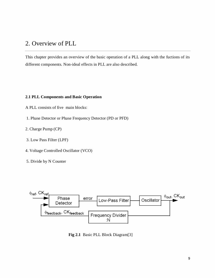
2. Overview of PLL
This chapter provides an overview of the basic operation of a PLL along with the fuctions of its
different components. Non-ideal effects in PLL are also described.
2.1 PLL Components and Basic Operation
A PLL consists of five main blocks:
1. Phase Detector or Phase Frequency Detector (PD or PFD)
2. Charge Pump (CP)
3. Low Pass Filter (LPF)
4. Voltage Controlled Oscillator (VCO)
5. Divide by N Counter
Fig 2.1 Basic PLL Block Diagram[3]
10
The Phase-frequency detector detects any phase differences between the input reference signal
and the feedback signal and thereafter generates an error signal. According to that error signal
the Charge-pump either increases or decreases the amount of charge to the low pass filter. This
charge either speeds up or slows down the voltage-controlled oscillator. The loop continues this
process until the phase difference between the input reference signal and the feedback signal is
zero or constant—that is the locked state. After the loop has achieved a locked state, the loop still
continues in the process but the output of each component stays constant. The output signal has
the same phase and/or frequency as the input reference signal .A frequency divider can be used
in the feedback loop in order to synthesize a frequency that is different from that of the reference
signal.
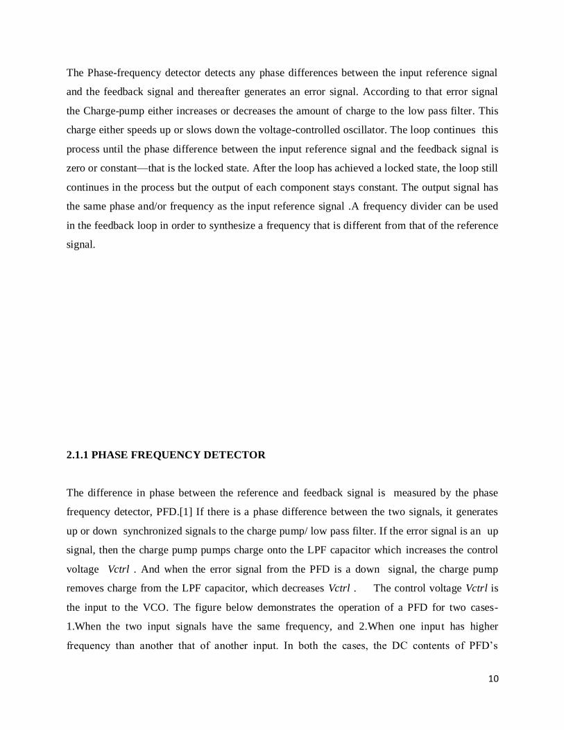
2.1.1 PHASE FREQUENCY DETECTOR
The difference in phase between the reference and feedback signal is measured by the phase
frequency detector, PFD.[1] If there is a phase difference between the two signals, it generates
up or down synchronized signals to the charge pump/ low pass filter. If the error signal is an up
signal, then the charge pump pumps charge onto the LPF capacitor which increases the control
voltage Vctrl . And when the error signal from the PFD is a down signal, the charge pump
removes charge from the LPF capacitor, which decreases Vctrl . The control voltage Vctrl is
the input to the VCO. The figure below demonstrates the operation of a PFD for two cases-
1.When the two input signals have the same frequency, and 2.When one input has higher
frequency than another that of another input. In both the cases, the DC contents of PFD‘s
11
outputs, UP and DN, provide information about phase or frequency difference. Thus, the LPF
serves the dual purpose of allowing only DC signals into the VCO and storing the charge from
the charge pump. The purpose of the VCO is to either increase or lessen the feedback signal
according to the error generated by the PFD.
If the PFD generates an up signal, the VCO speeds up. On the contrary, if a down signal is
generated, the VCO slows down. The output of the VCO is then fed back through the feedback
path to the PFD in order to recalculate the phase difference and the process continues till the
frequency is locked.
Fig.2.2 Phase Frequency Detector Operation[3]
12
2.1.2 CHARGE PUMP
A charge pump is a three position electronic switch which is controlled by the three states of
Phase-frequency detector. When the switch is in the UP or DOWN position, it delivers a pump
voltage to the loop filter. [4]When both UP and DOWN of Phase-frequency detector are off, that
is, N position, the switch is open, thus the loop filter is isolated from the charge pump and phase-
frequency detector.
2.1.3 LOOP FILTER
The loop filter is the heart of PLL.It is inevitable to choose the loop filter values correctly,as
inappropriate values may either lead the loop to oscillate for long without reaching the locked
state or it may so happen that once locked, small variations in the input data may cause the loop
to unlock. The PFD/CP/LPF combination contains a pole at the origin and VCO also contains a
pole at the origin. As the loop gain has two poles at the origin the instability arises. In order to
stabilize the system, we must modify the phase characteristics by adding a resistor in series with
the capacitor. The compensated PLL also suffers from a major shortcoming. Since the charge
pump drives the series combination of the resistor and capacitor, each time a current is injected
into the loop filter, the control voltage experiences a large surge. To overcome this problem
another capacitor is usually added in parallel with the RC network.
13
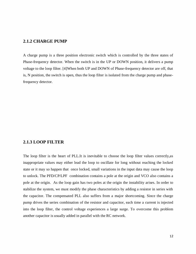
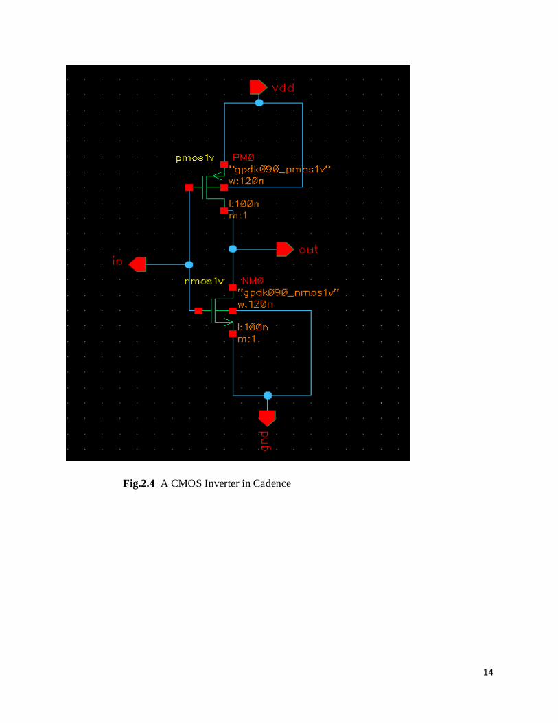
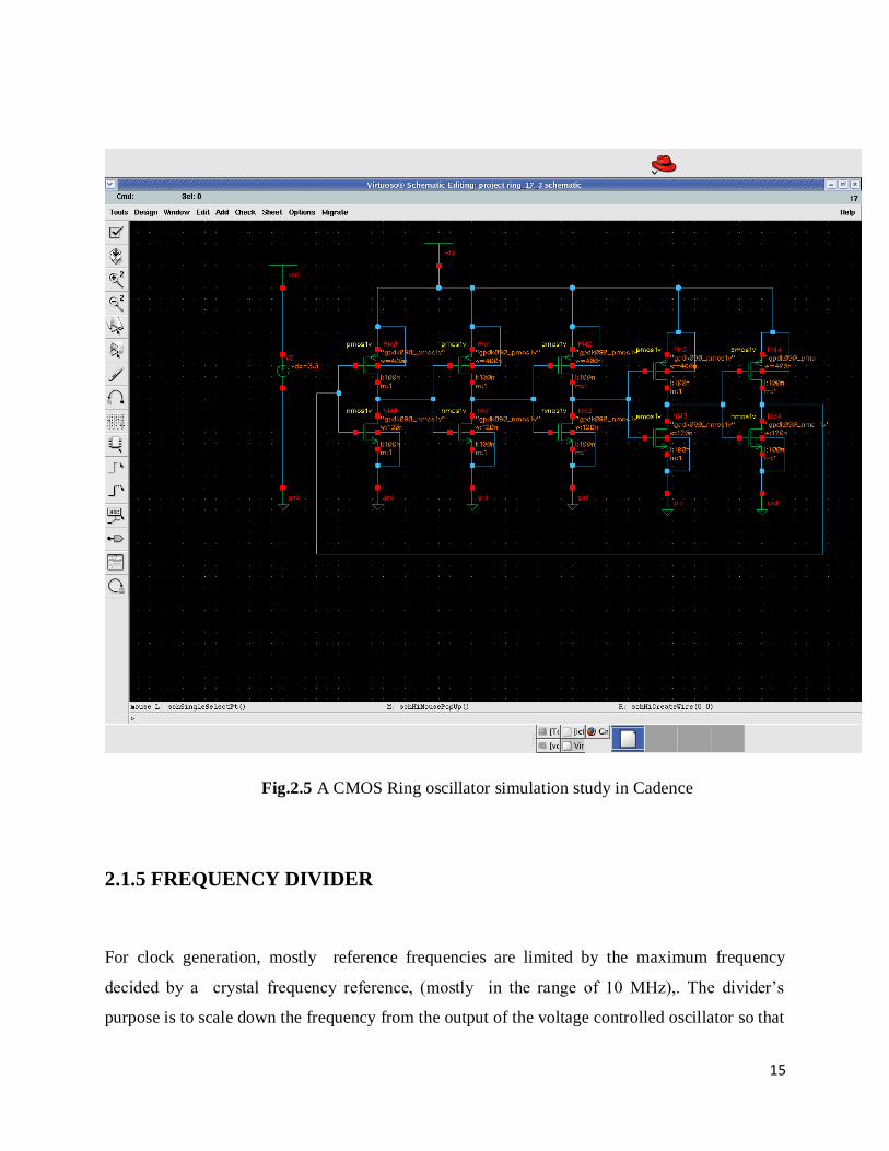
2.1.4 VOLTAGE CONTROLLED OSCILLATOR
An oscillator is an independent system that generates a periodic output without any input signal.
A voltage-controlled oscillator is an electronic oscillator designed such that its oscillation
frequency is controlled by a voltage input. . A CMOS ring oscillator shown is an example of an
oscillator .The frequency of oscillation is controlled by the applied DC voltage, while
modulating signals may also be fed into the VCO to cause frequency modulation or phase
modulation .The frequency of oscillation must be tunable for the phase of a PLL to be
adjustable. In our chosen example of an inverter ring oscillator, the frequency can be adjusted by
controlling the supply (voltage or current) of the inverters. The slope of frequency vs control-
signal curve at the oscillation frequency is called voltage-to-frequency conversion gain. Ideally,
for linear analysis to be applicable over a large range of frequencies, the voltage gain of the
VCO has to be relatively constant.
Fig.2.3 A 5-stage ring oscillator[3]
14
Fig.2.4 A CMOS Inverter in Cadence
15
Fig.2.5 A CMOS Ring oscillator simulation study in Cadence
2.1.5 FREQUENCY DIVIDER
For clock generation, mostly reference frequencies are limited by the maximum frequency
decided by a crystal frequency reference, (mostly in the range of 10 MHz),. The divider‘s
purpose is to scale down the frequency from the output of the voltage controlled oscillator so that
16
the system can operate at a higher frequency than the reference signal Thus the VCO has to be
designed such that the output of VCO is = N times the reference frequency. So the output of the
VCO is passed through a divide by N-counter and feedback to the input.
The D flip flop based divider has been chosen for this particular application because of practical
reasons. Some phase locked loops also include a divider between the oscillator and the feedback
input to the phase detector to produce a frequency synthesizer. A programmable divider is
especially useful in radio and transmitter applications, as a large number of transmit frequencies
can be produced from a stable and accurate quartz crystal–controlled reference oscillator.
2.2 PLL TERMINOLOGY
Lock Range
The range of input signal frequencies over which the loop can maintain the lock is called as Lock
Range or Tracking Range of PLL.
Pull in time
The total time taken by the PLL to capture the signal (or to establish the lock) is called as Pull in
Time of PLL. It is also called as Acquisition Time of PLL.
Capture range
The range of input signal frequencies over which PLL can acquire a lock is called as Capture
Range or Acquisition Range of PLL.
17
Bandwidth of PLL
Bandwidth is the frequency at which the PLL starts losing the lock with reference. The
bandwidth of a PLL is the measure of its ability to track the input clock and jitter.[5]
A high bandwidth PLL provides a fast lock time and tracks jitter on the reference clock source,
passing it through to the PLL output. A low bandwidth PLL filters out reference clock jitter, but
increases lock time.
2.3 NON-IDEAL EFFECTS IN PLL
Lots of imperfections remain in a practical PLL circuit. These lead to fluctuations in the control
voltage even after the locked state is achieved. These ripples change the VCO frequency, which
results in a non-periodic waveform. This section considers these non-ideal effects in PLL.
2.3.1 PHASE NOISE
Frequency stability of an oscillator is a measure of the degree to which it maintains the same
value of frequency over a given time period. The term Phase noise is generally used for
representing short term random frequency variations of a signal.[6] Non linear oscillators
naturally produce high phase noise. The unit used to describe phase noise is dBc/Hz (dB below
the carrier per Hz of bandwidth)
An ideal sine wave can be represented as:
V(t) = VoSin (2Pft)
where,
Vo=natural amplitude of the signal
f =natural frequency of oscillation
18
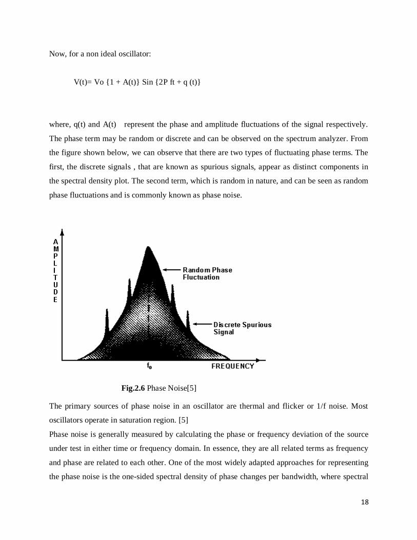
Now, for a non ideal oscillator:
V(t)= Vo {1 + A(t)} Sin {2P ft + q (t)}
where, q(t) and A(t) represent the phase and amplitude fluctuations of the signal respectively.
The phase term may be random or discrete and can be observed on the spectrum analyzer. From
the figure shown below, we can observe that there are two types of fluctuating phase terms. The
first, the discrete signals , that are known as spurious signals, appear as distinct components in
the spectral density plot. The second term, which is random in nature, and can be seen as random
phase fluctuations and is commonly known as phase noise.
Fig.2.6 Phase Noise[5]
The primary sources of phase noise in an oscillator are thermal and flicker or 1/f noise. Most
oscillators operate in saturation region. [5]
Phase noise is generally measured by calculating the phase or frequency deviation of the source
under test in either time or frequency domain. In essence, they are all related terms as frequency
and phase are related to each other. One of the most widely adapted approaches for representing
the phase noise is the one-sided spectral density of phase changes per bandwidth, where spectral
19
density is the energy distribution of the signal, expressed as energy per bandwidth. Measurement
of the noise sidebands on the either side of the spectral density curve gives information about the
phase noise of the signal.
Phase noise can be reduced to a great extent by the process of averaging.
2.3.2 JITTER
In many cases, the signals at the input, output and within a phase locked loop are binary signals,
.The term Jitter is generally used to refer to the time variation of a periodic signal in relation to
the clock.[7] This deviation can be in any form, phase, frequency or amplitude. It is generally
quantified in terms of RMS, peak to peak displacement etc. Generally, the events of interest are
the transitions in a signal.
Jitter Period is defined as the interval between two times of maximum effect (or minimum effect)
of a signal property that varies regularly with time and its inverse is known is Jitter Frequency
MODELLING OF JITTER
The jitter[5] in a signal is generally modeled by starting with a noise-free signal v and displacing
in time with a stochastic process j. The noisy signal becomes
Vn(t)=V(t+j(t))
where,
j is a process with zero mean and has the units of seconds and v is assumed to be a periodic
function.
20
The function j can be interpreted as a noise in time. Alternatively, it can expressed as phase
noise, using
φ(t) = 2πfo j(t),
There are various types of jitter like Random jitter. Deterministic jitter and Total jitter. To
mitigate the effect of jitter, different methods like using anti-jitter circuits, jitter buffers and
dejitterizers are used.
21
3. Circuit architecture of VCO
3.1 LC oscillators vs Ring oscillators
Generally, LC-oscillators[8] have exhibited good phase-noise performance with a low power
consumption. However, there are a few drawbacks. First, the tuning range of an LC-oscillator is
low as compared to ring oscillators. Therefore, frequency of the output may fall out of the
desired range in the presence of process-variation.
Second, the phase-noise performance of the oscillators is greatly dependent on the quality factor
of on-chip spiral inductors. For most digital CMOS processes, it is hard to get an inductor-
quality factor greater than three. As a result, some extra steps may be required for processing.
Finally, spiral inductors occupy a large chip -area, typically around 200 x 200 to 300 x 300
um2, which is undesirable because of cost and yield considerations. Also, ring oscillators can be
easily integrated on-chip without any extra processing steps. Moreover, ring oscillators normally
occupy less chip area, which improves both the yield and the cost. Having even number of delay
cells, the ring oscillators generate both in-phase and quadrature-phase outputs. The chosen VCO
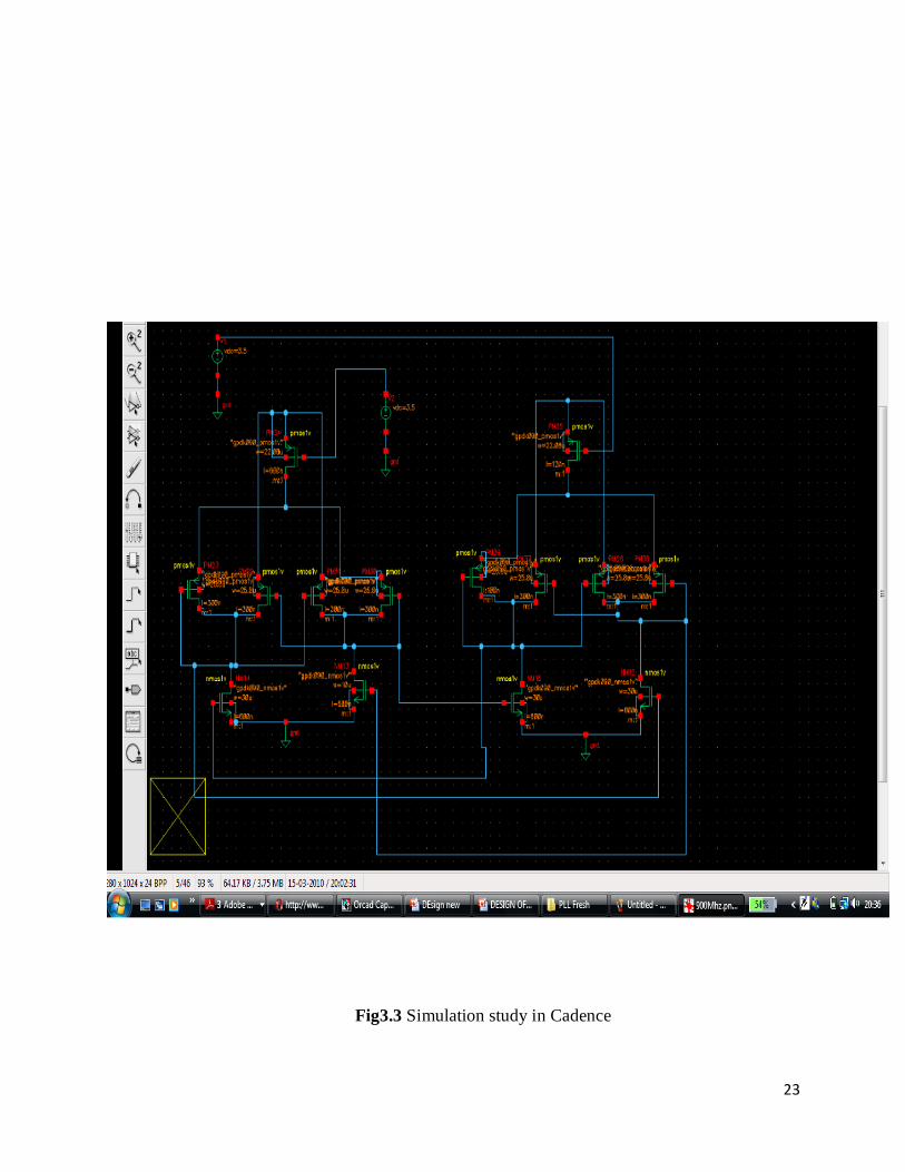
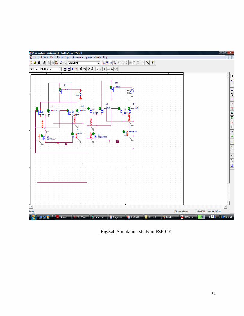
was simulated using Cadence and pSPICE. Screenshots from these schematics are shown.
22
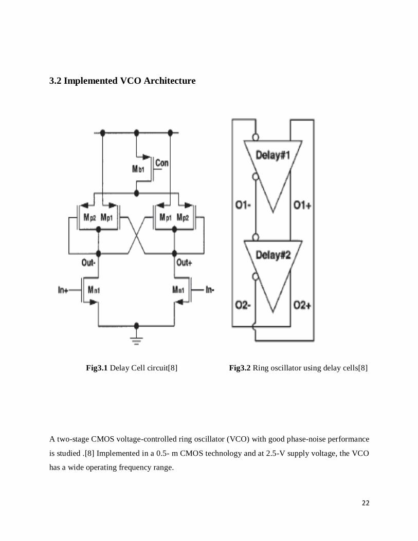
3.2 Implemented VCO Architecture
Fig3.1 Delay Cell circuit[8] Fig3.2 Ring oscillator using delay cells[8]
A two-stage CMOS voltage-controlled ring oscillator (VCO) with good phase-noise performance
is studied .[8] Implemented in a 0.5- m CMOS technology and at 2.5-V supply voltage, the VCO
has a wide operating frequency range.
23
Fig3.3 Simulation study in Cadence
24
Fig.3.4 Simulation study in PSPICE
25
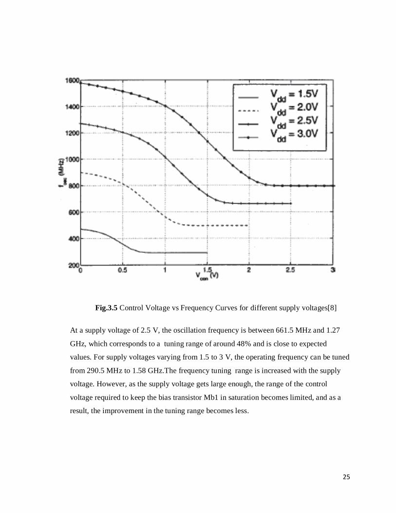
Fig.3.5 Control Voltage vs Frequency Curves for different supply voltages[8]
At a supply voltage of 2.5 V, the oscillation frequency is between 661.5 MHz and 1.27
GHz, which corresponds to a tuning range of around 48% and is close to expected
values. For supply voltages varying from 1.5 to 3 V, the operating frequency can be tuned
from 290.5 MHz to 1.58 GHz.The frequency tuning range is increased with the supply
voltage. However, as the supply voltage gets large enough, the range of the control
voltage required to keep the bias transistor Mb1 in saturation becomes limited, and as a
result, the improvement in the tuning range becomes less.
26
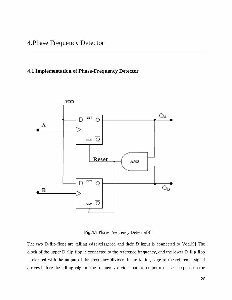
4.Phase Frequency Detector
4.1 Implementation of Phase-Frequency Detector
Fig.4.1 Phase Frequency Detector[9]
The two D-flip-flops are falling edge-triggered and their D input is connected to Vdd.[9] The
clock of the upper D-flip-flop is connected to the reference frequency, and the lower D-flip-flop
is clocked with the output of the frequency divider. If the falling edge of the reference signal
arrives before the falling edge of the frequency divider output, output up is set to speed up the
27
VCO. On the other hand, if the falling edge of the frequency-divider output arrives prior to the
falling edge of the reference signal that means the VCO frequency is faster than the reference
frequency and down is set to slow down the VCO. In either condition the falling edge of the late
signal activates the AND gate and two inverters to reset both up and down. The next cycle starts
with the next falling edge of the reference signal or the frequency divider output.
28
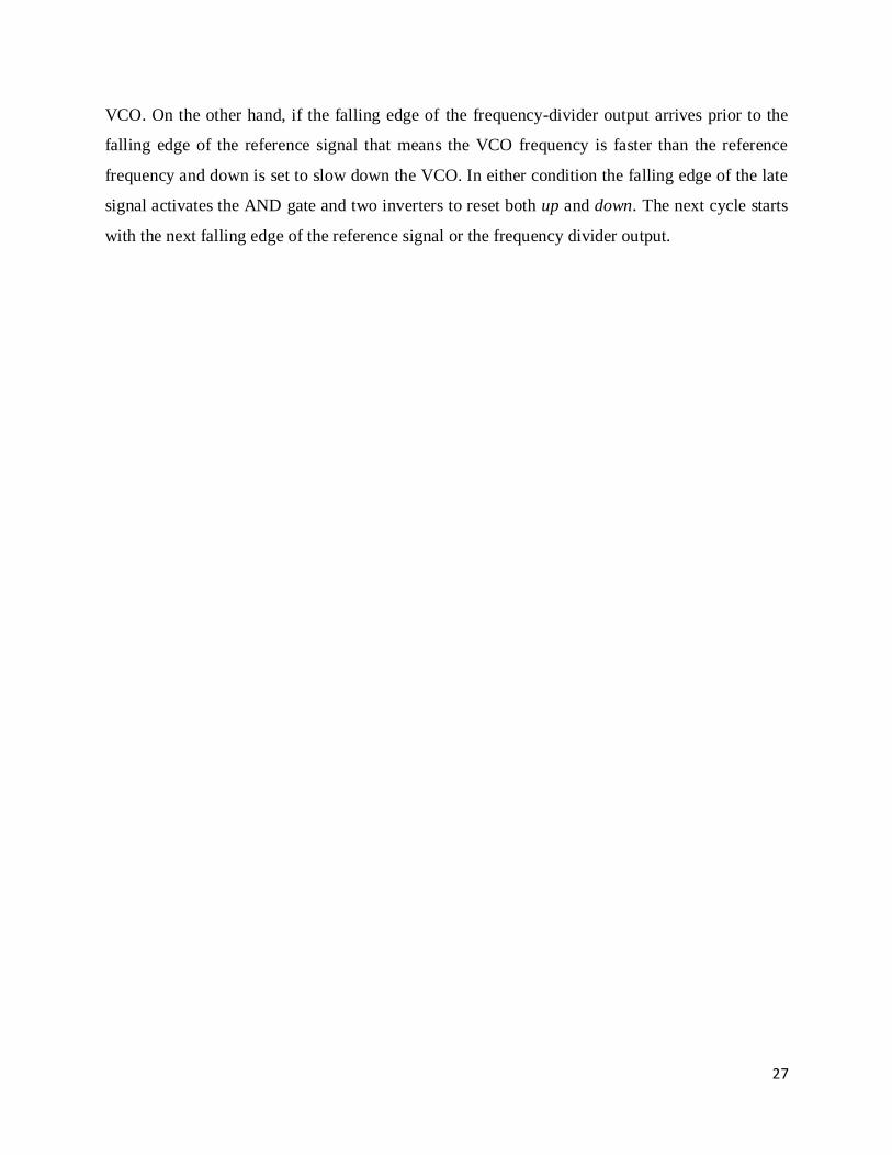
Fig.4.2. 3-input NAND gate implemented using CMOS.
29
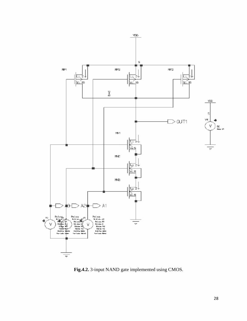
Fig. 4.3 3-input NAND gate in Cadence
30
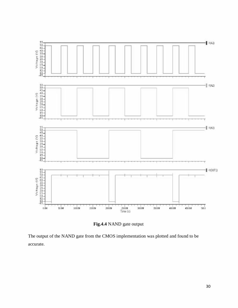
Fig.4.4 NAND gate output
The output of the NAND gate from the CMOS implementation was plotted and found to be
accurate.
31
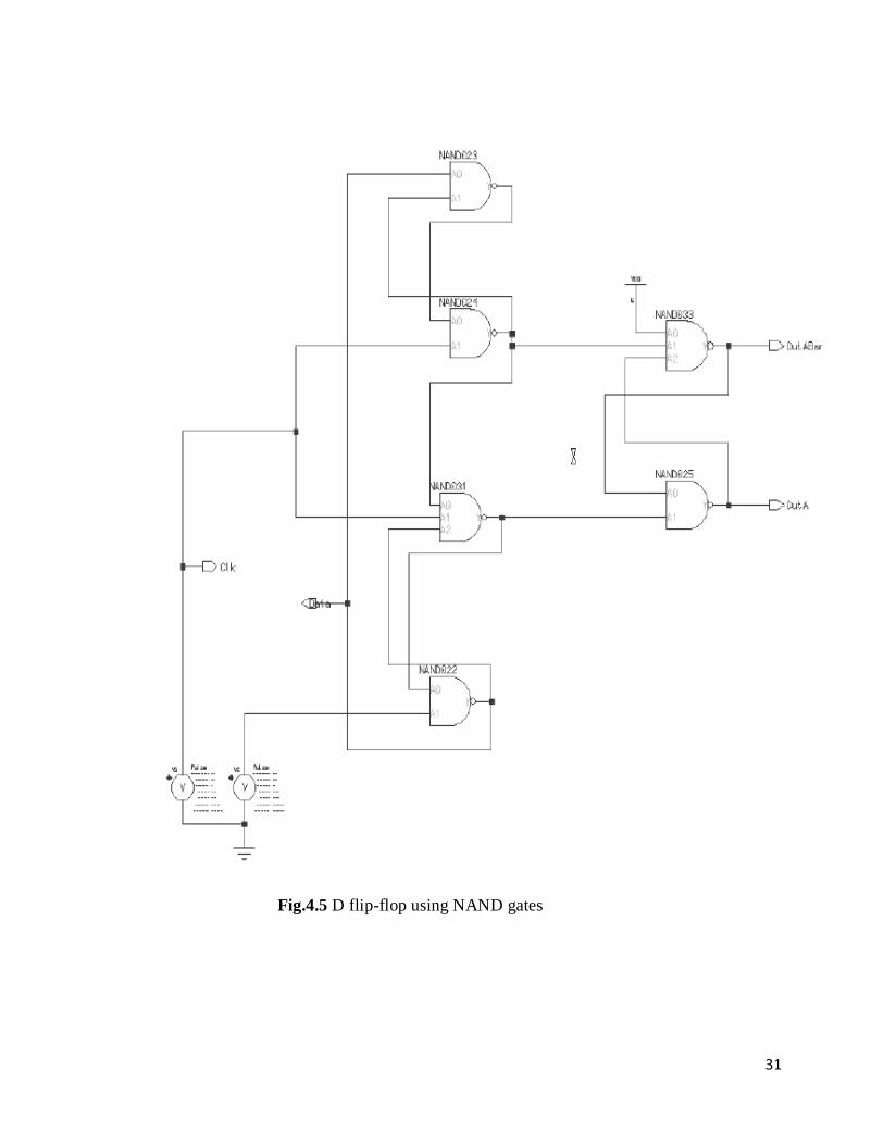
Fig.4.5 D flip-flop using NAND gates
32
.
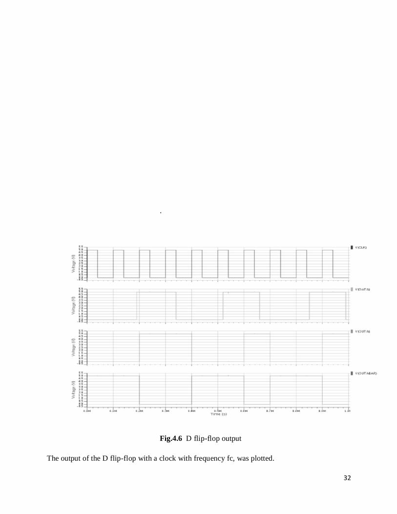
Fig.4.6 D flip-flop output
The output of the D flip-flop with a clock with frequency fc, was plotted.
33
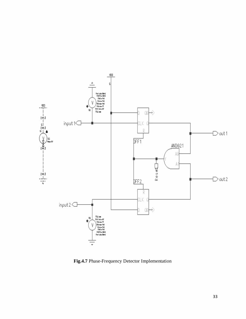
Fig.4.7 Phase-Frequency Detector Implementation
34
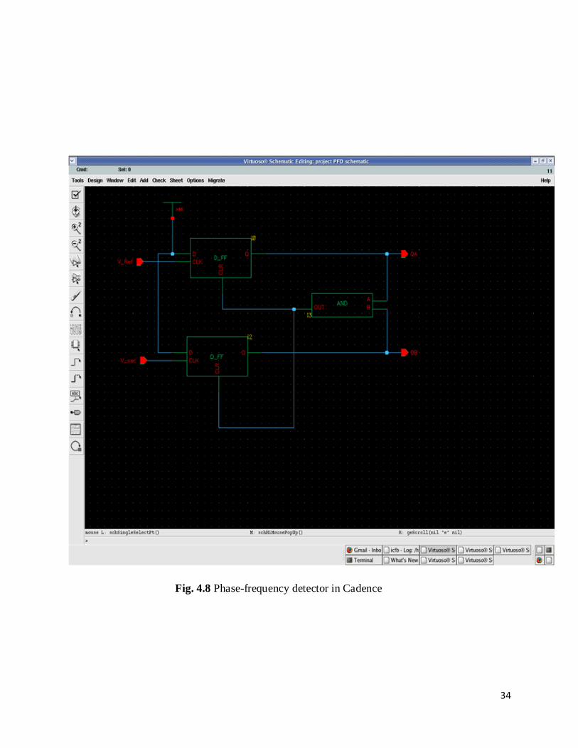
Fig. 4.8 Phase-frequency detector in Cadence
35
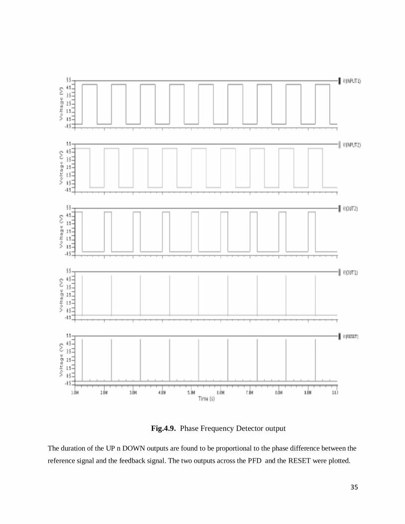
Fig.4.9. Phase Frequency Detector output
The duration of the UP n DOWN outputs are found to be proportional to the phase difference between the
reference signal and the feedback signal. The two outputs across the PFD and the RESET were plotted.
36
5. Conclusion
The present work studies the operation of a phase-locked loop and its different components. The
architectures were mostly studied in Virtuoso Analog Design Environment from Cadence. The
simulation studies reveal the behaviour of the individual components which were found to be as
expected.
37
References
[1] Phase-locked Loop
http://en.wikipedia.org/wiki/Phase-locked_loop
[2] Kristen Elserougi, Ranil Fernando, Luca Wei, ―Phase Locked Loop Design‖, School of
Engineering,Santa Clara University Santa Clara, California,June 20, 2006
[3] Mozhgan Mansuri, ―Low-Power Low-Jitter On-Chip Clock Generation‖, University of California,
Los Angeles 2003
[4] Floyd M. Gardner, ―Charge-Pump Phase-Lock Loops‖, IEEE Transactions On
Communications, Vol. Com-28, No. 11, November 1980
[5]http://www.altera.com
[6]Phase Noise
http://en.wikipedia.org/wiki/Phase_noise
[7]Jitter
http://en.wikipedia.org/wiki/Jitter
[8] William Shing Tak Yan and Howard Cam Luong, ―A 900-MHz CMOS Low-Phase-Noise
Voltage-Controlled Ring Oscillator‖, IEEE transactions on circuits and systems—II: Analog and
digital signal processing, Vol. 48, no. 2, February 2001
[9] Zhongtao Fu, Xiao Wang, Eugene Minh and Alyssa Apsel, ―A Fast Acquisition Phase
Frequency Detector for Phase-Locked Loops‖, Electrical and Computer Engineering, Cornell
University, Ithaca, NY 14853, USA

38


![Fractional/Integer-N Pll BasicsTI]_Fractional... · 2004-02-22 · components and their reaction to various noise sources, we will show that PLL is uniquely suited for generation](https://img.dokumen.tips/doc/110x75/5f24059f822ad3389b4f9fe1/fractionalinteger-n-pll-tifractional-2004-02-22-components-and-their-reaction.jpg)