Embed Size (px)
Citation preview
TKK Dissertations 41Espoo 2006
DESIGN, ANALYSIS, AND OPTIMIZATION OF RADIO FREQUENCY FRONT-ENDS FOR INTEGRATED WIRELESS RECEIVERSDoctoral Dissertation
Helsinki University of TechnologyDepartment of Electrical and Communications EngineeringElectronic Circuit Design Laboratory
Pete Sivonen
TKK Dissertations 41Espoo 2006
DESIGN, ANALYSIS, AND OPTIMIZATION OF RADIO FREQUENCY FRONT-ENDS FOR INTEGRATED WIRELESS RECEIVERSDoctoral Dissertation
Pete Sivonen
Dissertation for the degree of Doctor of Science in Technology to be presented with due permission of the Department of Electrical and Communications Engineering for public examination and debate in Auditorium S5 at Helsinki University of Technology (Espoo, Finland) on the 27th of October, 2006, at 12 noon.
Helsinki University of TechnologyDepartment of Electrical and Communications EngineeringElectronic Circuit Design Laboratory
Teknillinen korkeakouluSähkö- ja tietoliikennetekniikan osastoPiiritekniikan laboratorio

Distribution:Helsinki University of TechnologyDepartment of Electrical and Communications EngineeringElectronic Circuit Design LaboratoryP.O. Box 3000FI - 02015 TKKFINLANDURL: http://www.ecdl.tkk.fiTel. +358-9-451 2271Fax +358-9-451 2269E-mail: [email protected]
© 2006 Pete Sivonen
ISBN 951-22-8366-2ISBN 951-22-8367-0 (PDF)ISSN 1795-2239ISSN 1795-4584 (PDF) URL: http://lib.tkk.fi/Diss/2006/isbn9512283670/
TKK-DISS-2172
Otamedia OyEspoo 2006

AB
HELSINKI UNIVERSITY OF TECHNOLOGYP. O. BOX 1000, FI-02015 TKK
http://www.tkk.fi
ABSTRACT OF DOCTORAL DISSERTATION
Author Pete Sivonen
Name of the dissertation
Date of manuscript 13th of September, 2006 Date of the dissertation 27th of October, 2006
Monograph Article dissertation (summary + original articles)
Department
Laboratory
Field of research
Opponent(s)
Supervisor
(Instructor)
Abstract
Keywords radio frequency, radio receiver, direct conversion, low-noise amplifier, downconversion mixer
ISBN (printed) 951-22-8366-2
ISBN (pdf) 951-22-8367-0
ISBN (others)
ISSN (printed) 1795-2239
ISSN (pdf) 1795-4584
Number of pages 97 p. + app. 51 p.
Publisher Electronic Circuit Design Laboratory
Print distribution Electronic Circuit Design Laboratory
The dissertation can be read at http://lib.tkk.fi/Diss/2006/isbn9512283670/
Design, analysis, and optimization of radio frequency front-ends for integrated wireless receivers
X
Department of Electrical and Communications Engineering
Electronic Circuit Design Laboratory
Electronic Circuit Design
Doctor Jan Crols
Professor Kari Halonen
Doctor in Science (Technology) Aarno Pärssinen
X
This thesis consists of six publications and an overview of the research topic, which is also a summary of the work.The research described in this thesis is focused on the design, analysis, and optimization of RF front-ends for wirelesszero- and low-IF receivers. The main interest of the work is in the 1-4 GHz range and in CMOS and BiCMOStechnologies. Often, the RF front-end limits the performance of the entire direct conversion or low-IF radio receiver.
The emphasis in this work is on the challenges posed by mass production for the design of integrated RF circuits.Thus, the effects of packaging and ESD protection on the LNA performance are analyzed and circuit optimization anddesign methods for the packaged LNAs are examined. This thesis also studies circuit techniques for the stabilizationof the RF front-end performance against process and temperature variations. For this purpose, a gain stabilizationtechnique for tuned LNAs is proposed. By applying the proposed method, the voltage gain variation of the inductivelydegenerated LNA, which is the most popular LNA architecture, is shown to be reduced several decibels. As aconsequence, the radio receiver can more easily meet its specifications in the presence of IC process variations and theproduct yield is thereby improved. To improve the IIP2 of the mixer, a circuit technique for the cancellation of thesecond-order intermodulation distortion in downconversion mixer RF input stages is proposed. The presented methodis shown to improve the yield of the radio receiver by reducing the IIP2 sensitivity to mismatches and offsets.
Low supply voltage and low-frequency flicker noise present in sub-micron CMOS processes pose challenges for thedesign of direct conversion RF front-ends, especially for narrow-band systems such as GSM. However, since thedevelopment of low-voltage CMOS analog and RF circuits is economically advantageous, the design andoptimization of low-voltage CMOS RF front-ends are studied in this work.
The work summarizes the design, analysis, and optimization of several RF front-ends, LNAs, and mixers. One of theimplemented RF front-ends is integrated with an on-chip VCO as a part of larger direct conversion receiver chip. Oneis realized with an on-chip VCO as a standalone RF front-end. Also, a standalone CMOS LNA has been characterized.


AB
TEKNILLINEN KORKEAKOULUPL 1000, 02015 TKK
http://www.tkk.fi
VÄITÖSKIRJAN TIIVISTELMÄ
Tekijä Pete Sivonen
Väitöskirjan nimi
Käsikirjoituksen jättämispäivämäärä 13.9.2006 Väitöstilaisuuden ajankohta 27.10.2006
Monografia Yhdistelmäväitöskirja (yhteenveto + erillisartikkelit)
Osasto
Laboratorio
Tutkimusala
Vastaväittäjä(t)
Työn valvoja
(Työn ohjaaja)
Tiivistelmä
Asiasanat radiotaajuus, radiovastaanotin, suoramuunnos, vähäkohinainen vahvistin, alassekoitin
ISBN (painettu) 951-22-8366-2
ISBN (pdf) 951-22-8367-0
ISBN (muut)
ISSN (painettu) 1795-2239
ISSN (pdf) 1795-4584
Sivumäärä 97 s. + liit. 51 s.
Julkaisija Piiritekniikan laboratorio
Painetun väitöskirjan jakelu Piiritekniikan laboratorio
Luettavissa verkossa osoitteessa http://lib.tkk.fi/Diss/2006/isbn9512283670/
Radiotaajuusetupäiden suunnittelu, analyysi ja optimointi integroiduissa radiovastaanottimissa
X
Sähkö- ja tietoliikennetekniikan osasto
Piiritekniikan laboratorio
Piiritekniikka
Tohtori Jan Crols
Professori Kari Halonen
Tekniikan tohtori Aarno Pärssinen
X
Väitöskirja koostuu kuudesta julkaisusta ja tutkimustyön yleiskatsauksesta. Väitöskirjassa on tutkittu suoramuunnos-ja matalanvälitaajuuden radiovastaanottimien radiotaajuusetupäiden suunnittelua ja optimointia.Radiotaajuusetupäiden ominaisuuksia on myös analysoitu laajasti. Työn pääpaino on taajuusalueessa 1-4 GHz sekäCMOS- ja BiCMOS-integrointiteknologioissa. Käytännössä radiotaajuusetupäät usein rajoittavat suoramuunnos- jamatalanvälitaajuuden radiovastaanottimien suorituskykyjä.
Tutkimustyö keskittyy mikropiirien massatuotannon integroitujen radiotaajuuspiirien suunnittelulle aiheuttamiinhaasteisiin. Paketoinnin ja ESD-suojauksen vaikutuksia matalakohinaisien vahvistimien ominaisuuksiin analysoidaanja paketoitujen vahvistimien suorituskykyjen optimointia käsitellään. Tapoja vähentää radiotaajuusetupäidensuorituskykyjen vaihteluita prosessi- ja lämpötilavaihteluiden seurauksena tutkitaan. Esitetään tekniikka, jollamatalakohinaisien vahvistimien jännitevahvistuksien vaihteluita voidaan huomattavasti pienentää. Tapaalassekoittimien toisen kertaluvun leikkauspisteiden parantamiseksi esitetään. Käyttämällä hyväksi tutkimuksentuloksia radiovastaanottimien saantoja voidaan parantaa, koska vastaanottimet voivat helpommin saavuttaa niilleasetetut vaatimukset prosessi- ja lämpötilavaihteluista huolimatta.
Lyhyen viivanleveyden CMOS-prosessien alhainen käyttöjännite ja matalataajuinen 1/f -kohina ovat ongelmallisiaradiotaajuusetupäiden suunnittelussa, etenkin kapeakaistaisissa radiojärjestelmissä. Koska radiotaajuuspiirienintegrointi digitaali-CMOS-teknologioilla on kuitenkin taloudellisesti kannattavaa, tutkitaan tässä työssä alhaisenkäyttöjännitteen CMOS-radiotaajuusetupäiden optimointeja ja toteutuksia.
Tutkimustyössä on suunniteltu, analysoitu ja toteutettu useita radiotaajuusetupäitä, vähäkohinaisia vahvistimia jaalassekoittimia. Yksi radiotaajuusetupäistä on integroitu jänniteohjatun oskillaattorin kanssa samalle piirillle osanasuoramuunnosvastaanotinta. Yksi radiotaajuusetupää on toteutettu erillisenä integroituna piirinä jänniteohjatunoskillaattorin kanssa. Myös erillinen integroitu vähäkohinainen CMOS-vahvistin on karakterisoitu.


– vii –
Preface
The research for this thesis has been carried out at Nokia between 2002 and 2005. I wantto express my gratitude to all my present and former colleagues for their help and contri-butions to this work.
I would like to thank my supervisor, Prof. Kari Halonen, for giving me the opportu-nity to work on this thesis with a large degree of independence. I also warmly thank Prof.Asad Abidi and Prof. Francesco Svelto for reviewing my thesis and for their valuablecomments and suggestions. I wish to express my gratitude to D.Sc. Aarno Parssinen forinstructing me throughout my post-graduate studies and for his expert advice.
During my thesis work, I was lucky enough to belong to a powerful research team. Iam extremely grateful to my colleague Ari Vilander for his excellent ideas, advice, andcomments in the field of integrated RF circuits. I also wish to thank Seppo Kangasmaa forhis instruction and numerous discussions. In addition, I would like to thank Jussi-PekkaTervaluoto for fruitful discussions and advice, and for letting me benefit from his exper-tise in the design of integrated radio receivers and analog baseband circuits. Finally, Iwould like to express my gratitude to all my present and former superiors, Mikael Svard,Helena Pohjonen, Jarkko Posti, and Ph.D. Petteri Alinikula for their positive attitude to-wards my post-graduate studies and for giving me the opportunity to study for this thesiswhile working full time in industry.
The research for this thesis has been completely carried out while working full time inindustry. Thus, finding the motivation, time, and energy to write the articles and to com-plete the thesis by working during evenings and weekends only has not always been easy.However, now, almost at the end of this work, I have no doubt about its significance tome. I have been able to learn a significant number of new and interesting things, I havelearnt how to conduct academic research, and, most of all, I have learnt a scientific wayof thinking.
Big thanks go to all of my friends for various leisure-time activities. When lacking mo-tivation to write, there was always something else to do. My parents, Raili and Pertti,deserve my gratitude for supporting me throughout my studies.
Pete SivonenHelsinki, September 2006
– viii –
Contents
PREFACE vii
LIST OF SYMBOLS AND ABBREVIATIONS x
LIST OF PUBLICATIONS xv
AUTHOR’S CONTRIBUTION xvi
1 Introduction 11.1 Background . . . . . . . . . . . . . . . . . . . . . . . . . . . . . . . . . 11.2 Objectives of the work . . . . . . . . . . . . . . . . . . . . . . . . . . . 21.3 Contents of the thesis . . . . . . . . . . . . . . . . . . . . . . . . . . . . 2
2 Highly Integrated Radio Architectures for Wireless Receivers 32.1 Direct conversion receiver . . . . . . . . . . . . . . . . . . . . . . . . . 32.2 Low-IF receiver . . . . . . . . . . . . . . . . . . . . . . . . . . . . . . . 42.3 Choice of integration technology . . . . . . . . . . . . . . . . . . . . . . 52.4 Requirements for RF front-end . . . . . . . . . . . . . . . . . . . . . . . 7
3 Low-Noise Amplifier Design 103.1 LNAs for CMOS and BiCMOS technologies . . . . . . . . . . . . . . . . 103.2 Impacts of packaging and ESD protection . . . . . . . . . . . . . . . . . 113.3 Packaged inductively degenerated common-emitter LNA with ESD pro-
tection . . . . . . . . . . . . . . . . . . . . . . . . . . . . . . . . . . . . 133.4 Packaged inductively degenerated common-source LNA with ESD pro-
tection . . . . . . . . . . . . . . . . . . . . . . . . . . . . . . . . . . . . 223.5 LC-tuned load of LNA . . . . . . . . . . . . . . . . . . . . . . . . . . . 333.6 Variable gain in LNAs . . . . . . . . . . . . . . . . . . . . . . . . . . . 373.7 Biasing techniques . . . . . . . . . . . . . . . . . . . . . . . . . . . . . 39
4 Downconversion Mixer Design 424.1 Bipolar and BiCMOS downconversion mixers . . . . . . . . . . . . . . . 444.2 Low-voltage CMOS downconversion mixers . . . . . . . . . . . . . . . . 524.3 Second-order intermodulation distortion in active downconversion mixers 58
4.3.1 IM2 distortion suppression techniques in mixer RF input transcon-ductors . . . . . . . . . . . . . . . . . . . . . . . . . . . . . . . 59
4.3.2 Nonlinearity in switching stage . . . . . . . . . . . . . . . . . . 664.3.3 Calibration techniques . . . . . . . . . . . . . . . . . . . . . . . 67
5 Interface Issues in RF Front-End 685.1 Preselect filter-LNA . . . . . . . . . . . . . . . . . . . . . . . . . . . . . 685.2 LNA-downconversion mixer . . . . . . . . . . . . . . . . . . . . . . . . 685.3 Quadrature generation . . . . . . . . . . . . . . . . . . . . . . . . . . . 705.4 LO circuitry-downconversion mixer . . . . . . . . . . . . . . . . . . . . 72

– ix –
5.5 Downconversion mixer-analog baseband . . . . . . . . . . . . . . . . . . 73
6 Summary and Conclusions 77
References 79
Abstracts of Publications I-V 88

– x –
List of symbols and abbreviations
Symbols
β0 low-frequency current gain of bipolar transistorδ gate induced current noise factor∆A amplitude imbalance∆η mismatch in duty cycle∆gm mismatch between transconductances∆φ phase imbalance∆RL imbalance of load resistancesη bias dependent constantηnom nominal value of duty cycleγ channel current noise factorγN NMOS channel current noise factorγP PMOS channel current noise factorµ electron mobilityτF base transit time in forward directionΘ inversion layer mobility degradation factorω angular frequencyωT unity-current gain angular frequencyA base-emitter areaALO local oscillator amplitudeAv voltage gainc correlation coefficient between gate and drain noiseC capacitorCπ base-emitter capacitanceCb base-charging capacitanceCgs gate-source capacitanceCje base-emitter depletion layer capacitanceCLF leadframe capacitanceCm matching capacitanceCmd differential matching capacitanceCox oxide capacitanceCp equivalent parallel package parasitic capacitanceCpar parasitic capacitanceCps parasitic capacitance at source of cascode transistorD/A digital-to-analogf frequencyF noise factorf0 operation frequencyfT unity-current gain frequency

– xi –
G control voltagegd0 zero bias drain conductancegm transconductanceGm transconductanceI dc currentI in-phaseIB bias currentiC collector currentIC collector bias currenti2b mean-square shot noise in base currenti2c mean-square shot noise in collector currentiDS drain-source currentIDS drain-source bias currenti2d mean-square thermal noise in channel currenti2g mean-square gate-induced current noiseiin input currenti2n mean-square current noisei2on mean-square output current noiseiout output currentIPTAT PTAT bias currentIref reference bias currentISW switching pair bias currentIT tail currentkB Boltzmann’s constant 1.38 · 10−23J/KKf flicker noise coefficientK2gm
second-order nonlinearity coefficientL inductorL channel lengthLb base inductanceLbw parasitic bondwire inductanceLe emitter inductanceLg gate inductanceLm matching inductanceLs source inductanceM mutual inductanceM multiplying factornf number of gate fingersNFDSB double-sideband noise figurens number of sheet resistancesnp number of sheet resistancesq charge of electron 1.6 · 10−19C

– xii –
Q quadrature-phaseQ quality factorQind inductor quality factorR resistorReq equivalent resistorrb base resistanceRcm series resistance of matching capacitanceRE emitter resistancerg gate resistanceRg real part of impedance looking into gateRin input resistanceRL equivalent load resistanceRlb series resistance of base inductanceRlg series resistance of gate inductanceRls series resistance of inductanceroc output resistance of cascode amplifierRp shunt resistanceRpar parallel resistanceRref reference resistorRs source resistanceRser series resistanceRsh sheet resistanceRsub substrate resistanceS slope of LO signalS11 scattering parametert timeT absolute temperatureT impedance transformation ratioT LO periodT0 standard temperature 290 KV DC voltagevπ base-emitter voltageVDD supply voltageVB bias voltagevBE base-emitter voltageVBE base-emitter bias voltagevc control voltageVeff gate-source overdrive bias voltageVGS gate-source bias voltagevIIP2 differential input second-order intercept point voltage amplitudevIIP3 differential input third-order intercept point voltage amplitude

– xiii –
vin input voltagevLO LO voltage amplitudevout output voltagev2on mean-square output voltage noisevRF RF signalvs source voltageVt thermal voltageVT threshold voltageW channel widthZb impedance looking into baseZg impedance looking into gateZin input impedanceZL load impedanceZRs impedance looking into generator
Abbreviations
ADC analog-to-digital converterBiCMOS bipolar complementary metal oxide semiconductorBJT bipolar junction transistorBOM bills of materialCDMA code division multiple accessCMFB common-mode feedbackCMOS complementary metal oxide semiconductordc direct currentDR dynamic rangeDSB double-sidebandDSB-NF double-sideband noise figureDSP digital signal processingECL emitter coupled logicESD electrostatic dischargeFET field effect transistorGBW gain-bandwidth productGPS global positioning systemGSM global system for mobile communicationsIC integrated circuitICP input compression pointIF intermediate frequencyIIP2 input second-order intercept pointIIP3 input third-order intercept pointIM intermodulationIM2 second-order intermodulation

– xiv –
IM3 third-order intermodulationLNA low-noise amplifierLO local oscillatorMOS metal oxide semiconductorMOSFET metal oxide semiconductor field effect transistorNF noise figureNMOS N-channel metal oxide semiconductor transistorPA power amplifierPCB printed circuit boardPLL phase-locked loopPMOS P-channel metal oxide semiconductor transistorPTAT proportional-to-absolute temperatureQFN quad flat non-leaded packageRF radio frequencyRFIC radio frequency integrated circuitSCL source coupled logicSNR signal-to-noise ratioSOC system-on-a-chipSSB-NF single-sideband noise figureSTI shallow trench isolationV CO voltage-controlled oscillatorWCDMA wide-band code division multiple accessWLAN wireless local area network

– xv –
List of Publications
I. P. Sivonen, S. Kangasmaa, and A. Parssinen, ”A SiGe RF front-end with on-chipVCO for a GPS receiver,” in Proceedings of the European Solid-State Circuits Con-ference, pp. 435-438, Florence, Italy, Sep. 2002.
II. P. Sivonen, S. Kangasmaa, and A. Parssinen, ”Analysis of packaging effects and op-timization in inductively degenerated common-emitter low-noise amplifiers,” IEEETransactions on Microwave Theory and Techniques, vol. 51, pp. 1220-1226, Apr.2003.
III. P. Sivonen, A. Vilander, and A. Parssinen, ”A gain stabilization technique for tunedRF low-noise amplifiers,” IEEE Transactions on Circuits and Systems-I:RegularPapers, vol. 51, pp. 1702-1707, Sep. 2004.
IV. P. Sivonen and A. Parssinen, ”Analysis and optimization of packaged inductivelydegenerated common-source low-noise amplifiers with ESD protection,” IEEE Trans-actions on Microwave Theory and Techniques, vol. 53, pp. 1304-1313, Apr. 2005.
V. P. Sivonen, A. Vilander, and A. Parssinen, ”Cancellation of second-order intermod-ulation distortion and enhancement of IIP2 in common-source and common-emitterRF transconductors,” IEEE Transactions on Circuits and Systems-I:Regular Papers,vol. 52, pp. 305-317, Feb. 2005.
VI. P. Sivonen, J. Tervaluoto, N. Mikkola, and A. Parssinen, ”A 1.2-V RF front-endwith on-chip VCO for PCS 1900 direct conversion receiver in 0.13-µm CMOS,”IEEE Journal of Solid-State Circuits, vol. 41, pp. 384-394, Feb. 2006.
Throughout the overview, these papers will be referred to by Roman numerals.

– xvi –
Author’s Contribution
As a general guideline, in each paper of which I was the first author, the main responsi-bility for the manuscript has been mine.
In Paper I, I carried out the circuit design, analysis, simulations, and measurements ofall the circuits in the RF front-end, excluding the VCO, which was completely designedand measured by Seppo Kangasmaa. The system partitioning was done together withSeppo Kangasmaa. I was responsible for the top-level RF simulations. The paper itselfwas completely written by the author and revised by Seppo Kangasmaa and Aarno Parssi-nen.
In Paper II, I had the responsibility for the theoretical analysis, circuit design, and simu-lations. I was also responsible for the LNA and RF front-end measurements. Seppo Kan-gasmaa and Aarno Parssinen were involved in this work as instructors. The manuscriptitself was entirely written by the author and revised by Seppo Kangasmaa and AarnoParssinen.
The gain stabilization technique presented in Paper III was developed in co-operationwith Ari Vilander. I was responsible for all the theoretical work presented in this paper.I derived the design equations for the gain stabilization technique and also presented thenecessary conditions for the technique to operate properly. In addition, I was responsiblefor the LNA and LC-tuned load simulations presented in this paper. The paper was com-pletely written by the author and revised by Aarno Parssinen.
I carried out the theoretical analysis, circuit design, and simulations in Paper IV. I wasalso responsible for the LNA measurements. The paper was entirely written by the authorand revised by Aarno Parssinen.
The IIP2 enhancement circuit proposed in Paper V was invented by myself together withAri Vilander. In the paper, I was responsible for all the theoretical work. In addition,I performed all the simulations and wrote the paper completely. Aarno Parssinen gavevaluable comments for the manuscript and he revised the paper.
In Paper VI, I carried out the circuit design of LNA, I and Q mixers, frequency dividers,and LO buffers. Niko Mikkola designed and measured the VCO, while Jussi Tervaluotodesigned the analog baseband circuitry. I performed the top-level simulations togetherwith Jussi Tervaluoto. We also co-operated in the design of the interface between themixer and analog baseband. The system partitioning work was mainly done by Jussi Ter-valuoto. Jukka Kuivalainen and Tuomas Leinonen provided significant assistance in theRF front-end measurements. Finally, I was responsible for writing the paper, althoughJussi Tervaluoto and Aarno Parssinen gave valuable comments and suggestions for themanuscript.
– 1 –
1 Introduction
1.1 Background
The mobile wireless communications market has been growing very rapidly in recentyears. The rapid growth has been aided by low-power, low-cost, and high-performanceradio frequency integrated circuits (RFICs). Increasing the level of integration has beenthe major target in the design of transceivers for wireless applications. Highly integratedRFIC reduces the printed circuit board (PCB) area and complexity while lowering thecomponent cost.
In recent years, direct conversion and low-intermediate frequency (IF) wireless radio re-ceiver architectures have gained increasing attention [1]- [7], because in these topologiesa very high level of integration can be obtained. Moreover, radio transceivers and com-plete systems-on-a-chip (SOC) realized in pure complementary metal oxide semiconduc-tor (CMOS) technology are rapidly appearing in a wireless market that for years wasdominated by bipolar and BiCMOS implementations [8]. RF CMOS has already becomethe dominant IC technology for non-cellular wireless applications such as Bluetooth [7],Global Positioning System (GPS) [9], and wireless local area network (WLAN) [10].However, most of the commercial transceivers for cellular applications such as globalsystem for mobile communications (GSM) [11], [12], [13], wide-band code division mul-tiple access (WCDMA) [14], [15], and CDMA [16], [17], [18] are currently implementedin BiCMOS technology.
Development work for mass production applications poses challenges for the design ofintegrated RF circuits. Firstly, in order to maximize the product yield, the circuit per-formance must be stabilized against process, temperature, and supply voltage variations.For this purpose, appropriate circuit techniques and biasing methods must be utilized.Secondly, the power consumption, size and cost of the component parts must be mini-mized. In consumer electronics applications, these requirements are met by maximizingthe level of integration while minimizing the number of external components and siliconarea. The power consumption is also minimized by making intelligent decisions at boththe architectural and circuit-design levels, and by careful system and circuit co-design.Next, commercial RFICs must also be mounted in a package to protect the circuits frommechanical stress and to ease the automatic soldering of chips to PCB. In addition, forreliability reasons, off-chip interfaces must be protected by electrostatic discharge (ESD)protection structures. Unfortunately, at RF frequencies, the package and ESD parasiticscannot be neglected and they must be carefully taken into account in the circuit design.Finally, the fact that the supply voltage of integrated RF circuits must scale down withtransistor technology poses additional challenges for the analog and RF circuit design.The challenge is how to achieve a large dynamic range and meet the RF specifications,which do not relax. Low supply voltage limits the upper end of the dynamic range andprevents the stacking of several devices.
– 2 –
1.2 Objectives of the work
The research described in this thesis focuses on the design, analysis, and optimizationof RF front-ends for wireless zero- and low-IF receivers. Both CMOS and BiCMOSimplementations are discussed. Often, the RF front-end limits the performance of theentire direct conversion or low-IF receiver. The emphasis is on the challenges posed bythe mass production to the design of integrated RF circuits. Thus, the effects of packagingand ESD protection on the performance of low-noise amplifiers (LNAs) are analyzed andcircuit optimization methods for the packaged LNAs are studied. Also, circuit techniquesfor the stabilization of the RF front-end performance against process and temperatureare presented. In addition, a biasing circuit technique for the cancellation of the second-order intermodulation distortion in downconversion mixer RF stages is proposed. Thepresented approach is shown to improve the yield of the entire zero- or low-IF radioreceiver by improving the second-order intercept point (IIP2) of the mixer. Finally, thisthesis also concentrates on the design and optimization techniques for 1.2-V low-voltageRF front-ends realized in pure digital CMOS.
1.3 Contents of the thesis
This thesis is divided into two parts. In the first part, an overview of the monolithic RFfront-end design issues for direct conversion or low-IF receivers is given to summarizethe technical work that has been carried out. In the technology aspects, the overviewis focused on CMOS and BiCMOS processing technologies. In Chapter 2, the directconversion and low-IF receiver architectures are discussed and the factors influencing thechoice of the integration technology are emphasized. Next, typical requirements given forthe RF front-end in wireless receivers are discussed. A detailed description of the designof LNAs and active downconversion mixers are given in Chapters 3 and 4, respectively.In Chapter 5, the RF front-end interface issues are considered. The second part of thethesis contains the published papers.
– 3 –
2 Highly Integrated Radio Architectures for WirelessReceivers
Nowadays most of the reported wireless receivers are based either on direct conversion orlow-IF architectures, because these receiver topologies allow a very high level of integra-tion and low cost. Zero- and low-IF receivers also reduce radio complexity by removingthe need for off-chip IF filters and multiple local oscillator (LO) signals. Often, only asingle external filter, which is the RF band-selection filter, is required. The channel se-lection filtering, either in analog or digital domain, can be performed on silicon. Thus,since in zero- or low-IF receivers there is no need to drive impedance-matched off-chipnodes, the needed chip pin count is reduced and the impedance levels between the differ-ent blocks can be optimized for maximal dynamic performance. Finally, direct conversionand low-IF architectures permit efficient integration of multimode receivers. In general,the selection of the radio receiver architecture between the zero- or low-IF topology ismade on the basis of the radio system requirements and on the integration technologyavailable.
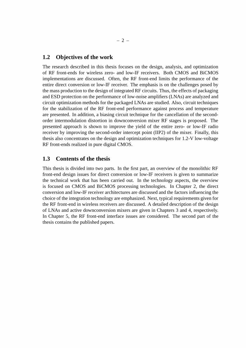
2.1 Direct conversion receiver
A block diagram of the direct conversion receiver is shown in Fig. 1(a). The antennafeeds the received RF signal to a bandpass filter that performs the preselection of the re-ceived RF band. The LNA, which is usually the first integrated block of the receiver,amplifies the RF signal in order to reduce the noise contributions of the following stages.The LNA can be connected directly (or through an external filter) to the downconversionmixers. The mixers drive the analog baseband containing low-pass filters and gain stages.
A direct conversion receiver downconverts the band of interest directly to a zero frequencyand utilizes low-pass filtering to reject nearby interference signals. An analog or digitallow-pass filter can also be employed to select the desired channel and to reject all adjacentchannels. The direct conversion architecture avoids the image suppression problem be-cause the image consists of the channel itself at zero IF [19]. For the same reason, typicalgain mismatches and phase errors in the two I and Q branches cause only a small loss inthe detected signal-to-noise ratio (SNR). Thus, typically it is sufficient to reject the imageby, say, 15-20 dB or so and this is easily obtained with conventional quadrature conver-sion [20]. However, the direct conversion architecture has several well-known problemssuch as dc offset, flicker noise, and even-order distortion, which must be considered inthe design [3], [19], [21]. In wide-band communication systems such as WLAN, CDMA,and WCDMA, the realization of the zero-IF receiver becomes viable, because the large-signal bandwidth makes the system less sensitive to dc offset and 1/f noise. Accordingly,both CMOS and BiCMOS direct conversion receivers for WLAN, CDMA, and WCDMAapplications have been proposed in the recent past [22], [23], [16], [18], [24], [3], [25].On the other hand, since CMOS zero-IF receivers, in general, suffer from much higherflicker noise than their bipolar or BiCMOS counterparts, the direct conversion receiversfor narrow-band systems, such as GSM, can be more easily implemented in BiCMOStechnologies [26]. Nevertheless, GSM zero-IF receivers manufactured in CMOS technol-ogy have also been reported recently [27], [Paper VI].
– 4 –
Figure 1: Block diagram of (a) direct conversion receiver and (b) low-IF re-ceiver, assuming analog image rejection. In the case of digital image rejection,(a) also represents a block diagram of a low-IF receiver.
2.2 Low-IF receiver
In a zero-IF receiver, dc offset and flicker noise cannot be easily eliminated without re-moving valuable spectral energy around the dc in the downconverted spectrum [20]. Onthe contrary, in low-IF receivers, the band of interest is translated to a near-zero-IF fre-quency in such a way that the dc offset can be easily removed and 1/f noise has lessimpact on receiver sensitivity [28]. The intermediate frequency of a low-IF architectureis usually chosen in such a way that the image channel is the adjacent channel, in whichthe maximum allowed signal power is kept much lower than in the other channels. Thissolution keeps the image-rejection requirement within affordable levels. Nevertheless, ingeneral, the requirements for the amplitude (∆A) and phase imbalance (∆φ) between theI and Q paths are more stringent compared to the direct conversion receiver. For instance,in a GSM low-IF receiver, it is necessary that the image-rejection ratio is at least 32 dBor, equivalently, ∆A ≤ 0.3 dB and ∆φ ≤ 2o [4], whereas in a direct conversion receiverit is usually sufficient if ∆A ≤ 1 dB and ∆φ ≤ 5o. Without tuning, the repeatable imagerejection of a simple quadrature mixer is limited to about 40 dB [20]. The image channelmay be rejected by mixing the RF with the quadrature phases of the LO, and filtering theresult with a Hilbert or polyphase filter at the IF, as shown in Fig. 1(b). Unfortunately,compared to the zero-IF architecture, on-chip analog image rejection with a passive [29]or active [9] polyphase filter increases the complexity and power consumption of the re-ceiver. An active low-pass filter (for instance, a channel filter) at zero-IF always obtainsa given dynamic range with lower power than a band-pass filter with the same passband

– 5 –
centered at some nonzero-IF [30]. Finally, although it is possible to reject the image ina digital signal processing (DSP) by digitizing separate I and Q paths after the mixer,the analog-to-digital converter (ADC) must digitize the image as well and therefore musthave higher dynamic range (DR) [4], [31]. As a conclusion, the use of low-IF receiverarchitecture is feasible when the mirror image suppression requirements are moderate,as, for instance, in reported low-IF CMOS receivers for GPS [32], [9], Bluetooth [7], orGSM [4].
2.3 Choice of integration technology
Most of the modern wireless radio receivers are implemented either by using CMOS orBiCMOS technologies. In this section, the benefits, drawbacks and trade-offs of thesetechnology options are discussed.
In designs where time to market is critical, the availability of accurate simulation modelsis essential. Fortunately, at the moment, the existing temperature, high-frequency small-signal and noise models for both bipolar junction transistors (BJTs) and MOS devicesare adequate for predicting accurately the performance of RF circuits. For instance, theRF performance of MOS transistors can be modeled accurately by using MOS Model 11,BSIM3, or BSIM4 with model extrinsic parasitic gate, substrate, drain and source resis-tances. On the other hand, the non-quasi-static RF model, based on the channel segmenta-tion, is capable of predicting both the drain and gate-induced current noise accurately [33].
Generally, to achieve comparable noise factors and transconductances, bipolar topolo-gies require less current than MOS versions due to the better gm/I ratio [34], [35], thusmaking it easier to save power. However, the two types of transistors offer a roughly com-parable dynamic range at a given bias [30], [36]. For instance, when designed for equallinear full scale, a degenerated bipolar differential pair gives the same transconductanceper unit bias current as the corresponding MOSFET transconductor [36]. In general, thedynamic range is limited at the lower end by the noise spectral density integrated acrossthe channel bandwidth, and at the upper end by the large signal swing that distorts gainand defines the intercept point.
The performance of bipolar RF circuits can be easily and effectively stabilized againsttemperature, supply and process variations by employing biasing techniques such asProportional-to-Absolute Temperature (PTAT) or bandgap circuits [37], [38]. On theother hand, although similar biasing techniques, such constant-transconductance (gm)circuit [39], for CMOS circuits exist, the design of robust RF MOS circuits is usuallya more difficult task due to the complicated parameter variations of MOS devices withtemperature and process [40]. As a result, open loop small-signal RF MOS circuits, suchas amplifiers and mixers, experience larger process and temperature variations than theirbipolar counterparts.
In general, BJTs provide better matching and lower flicker noise than CMOS devices.For, these reasons, the realization of a direct conversion receiver with BiCMOS tech-
– 6 –
nology, especially for narrow-band applications such as GSM, is easier than with pureCMOS technology. For instance, the use of BJTs as switches in active mixer and possiblyin some parts of analog baseband (i.e. at the input stage of op-amps) results in lowerlow-frequency noise than with MOS devices only [6], [41]. Moreover, better matchingdue to the use of BJTs in appropriate circuits results in better second-order intermod-ulation (IM2) performance, which is essential in direct conversion and also in low-IFreceivers [28], [42]. The availability of BJTs in BiCMOS technology should not, how-ever, preclude the use of CMOS in those RF applications where CMOS is superior, forexample in voltage controlled oscillators (VCOs) [6], [8].
Although BiCMOS technology provides some benefits over the pure CMOS technol-ogy in circuit design, and, possibly, performance wise, radio on pure CMOS offers apotential for cost reduction, since the mask count in pure CMOS technology is typicallysmaller than in the corresponding BiCMOS technology [43]. Moreover, integration of RFtransceiver functions on standard digital CMOS technology paves the way to the realiza-tion of a single-chip radio modem. A digital baseband and RF transceiver in the sametechnology increases the level of integration and reduces the bills of material (BOM).CMOS technology has also the ability to operate at lower supply voltage (e.g., 1-2 V)than the BiCMOS technology. This is due to the fact, that, typically each BJT has a turn-on voltage of approximately 0.7-0.8 V and thus the absolute minimum supply voltage forBJT circuits is about 1.4-1.6 V (assuming, at maximum, two stacked transistors) [44]. Onthe contrary, the turn-on voltages of MOS devices can be significantly affected by dopingand therefore in modern CMOS processes several different threshold voltages (VT ), suchas high-, standard- and low-VT are available. For instance, transistors with low-VT can beutilized in analog or digital circuits, where speed is important. On the other hand, deviceswith high-VT are useful when the low power consumption of the digital parts due to theleakage currents is critical.
Currently, RF CMOS technology dominates IC technology for non-cellular wireless ap-plications such as Bluetooth and WLAN whereas most of the transceivers for cellularapplications such as GSM and WCDMA are implemented in BiCMOS technology. How-ever, all-CMOS radio transceivers are already making inroads into the cellular wirelessmarket [8]. The challenges of CMOS technology are overcome by careful architecturaldecisions and by appropriate circuit-design techniques. Wherever possible, the avail-ability of high-density logic should be exploited by pushing the design complexity intothe digital domain [45]. Nevertheless, while a higher transistor unity-current gain fre-quency (fT ) and the consequent speed is welcome in fine-line CMOS with gate lengthsof 0.13 µm or below, the lower supply voltage of 1.2 V or below poses additional chal-lenges.
– 7 –
2.4 Requirements for RF front-end
In this section, typical requirements given for the direct conversion or low-IF receiver RFfront-end are discussed. In this thesis, the RF front-end refers to the LNA, I and Q mixers,and LO quadrature generation circuit excluding the VCO and phase-locked loop (PLL).The LNA and mixer together determine the front-end performance. Thus, an optimumperformance can only be obtained by co-designing the front-end circuits. Moreover, inpractice, the RF front-end dominates the linearity and noise performance of the entirezero- or low-IF receiver.
As seen from Fig. 1, the RF front-end architecture in both zero- and low-IF receivertopologies is the same. Actually, if the image rejection is performed in the digital do-main, Fig. 1(a) also represents the block diagram of both receiver topologies. In general,the requirements given for the zero- and low-IF receiver RF front-end for certain applica-tions are also very similar. However, the requirements nevertheless usually differ at leastin terms of I and Q balance, dc offset, low-frequency noise, and second-order nonlinearity.
The RF front-end of a wireless receiver must simultaneously meet several requirements[46]. First, as shown in Fig. 1, an RF front-end is practically always preceded by an off-chip filter. Accordingly, the RF input impedance of the front-end has to be designed tomatch the characteristic impedance, e.g., 50 Ω, of the filter. If the terminating impedancesof the RF preselection filter differ from the specified characteristic impedance, the resultsmay be a large ripple in the passband and a poorer transition band of the filter. Secondly,the input-referred noise, and thus the noise factor (F) of the front-end, must be sufficientlylow to enable detection of weak input signals. In particular, the noise factor for the directconversion presented in Fig. 1(a) is given as [47], [2]
F = F1 +F2 − 1(Av1
2
)2 +F3 − 1(
Av12
×Av2)2 + ... (1)
where Avi represents the voltage gain of the ith block and F1, F2, and F3 are the noisefactors of the LNA, mixer, and low-pass filter, respectively. F2 and F3 are defined asthe input-referred noise voltage of each circuit scaled to the noise in a hypothetical 50-Ωresistor [30]. The first two terms in Eq. (1) represent the noise factor of the RF front-end itself. Moreover, from Eq. (1) it is seen that the front-end gain (Av1 × Av2) mustbe sufficiently high to overcome the noise contributions of the following circuits (i.e. thelow-pass filter shown in Fig. 1(a)), which may otherwise degrade the receiver sensitivity.Typically, the maximum voltage gain of the RF front-end is in the range of 20 dB to 40 dB.However, depending on the mixer-analog baseband interface, the RF front-end can utilizecurrent- instead of voltage-mode signal processing at the mixer output [4], [Paper VI].Thus, in that particular case, the front-end gain is expressed more conveniently in termsof transconductance instead of voltage gain. Finally, to improve the receiver linearity withhigh RF input signal levels, the gain of the RF front-end is often variable.
Flicker noise at zero or low IF can be troublesome, particularly in CMOS receivers. Thenoise factor of CMOS mixers, baseband amplifiers, and filters may be much higher at low

– 8 –
frequencies than those based on estimates of thermal noise alone. Accordingly, besidesthe low level of thermal noise, the 1/f noise corner frequency of the RF front-end mustbe located at a sufficiently low frequency to ensure that the flicker noise does not worsenthe integrated noise factor more than is tolerable [48]. Given the particular integratednoise factor target and level of thermal noise, the RF front-end for a zero-IF receiver mustnaturally provide a lower 1/f corner frequency than for a corresponding low-IF receiver.
Due to the third-order nonlinearity of the RF front-end, two large undesired signals atthe adjacent channels can create a third-order intermodulation (IM3) product at the de-sired channel [49]. If the energy of the IM3 product is sufficiently large, it can overlapand corrupt the weak desired signal. Accordingly, the front-end must have a sufficientlylarge third-order intercept point (IIP3) to withstand this effect. In particular, the IIP3 forthe direct conversion receiver presented in Fig. 1(a) is given as [2]
1
IIP3=
1
IIP31
+A2v1
IIP32
+(Av1 × Av2)
2
IIP33
... (2)
where IIP3i is the IIP3 of the ith block measured in terms of the input signal powerdissipated in a reference 50-Ω resistor. Again, the first two terms in Eq. (2) represent theIIP3 of the RF front-end itself. From Equations (1) and (2) it is seen that, although a highfront-end gain reduces the noise contributions of the downstream stages, the gain can notbe arbitrarily large, because, otherwise, the receiver linearity is degraded.
In addition to IIP3, the RF front-end must have a sufficiently high input compressionpoint (ICP) to tolerate large blocking or interference signals. A strong signal can reducethe front-end small-signal gain when the front-end is receiving a weak desired signal, orit can cause a rise in the noise level [50].
One of the most severe limitations on the use of direct conversion techniques, and alsoan issue in a low-IF receivers, is the need for a very high second-order intercept point(IIP2) [42]. In the RF front-end, the second-order intermodulation introduces undesirablespectral components at the baseband, which degrade the receiver sensitivity. For instance,if two strong interferers at frequencies f1 and f2 close to the channel of interest experienceeven-order distortion, they generate a low-frequency interference signal at the frequencyf1−f2. Again, to withstand this effect, the IIP2 of the RF front-end must be high enough.
In a zero-IF receiver, the downconverted band extends to a zero frequency. Accordingly,extraneous offset voltages can corrupt the signal. Thus, in order to prevent the basebandcircuits or ADC from saturating, the dc offset voltage at the RF front-end output must besufficiently low. Compared to the zero-IF architecture, low-IF topology is less susceptibleto dc offset [4]. In addition to dc offset, the LO leakage to the front-end RF input must notexceed a certain level. The leakage of the LO signal to the antenna can create radiationinterference in the band of other users using the same or nearby channel [21].
Amplitude imbalance (∆A) and phase error (∆φ) between the I and Q paths of the RFfront-end can corrupt the downconverted signal constellation and raise the bit rate [21].

– 9 –
As discussed in Section 2.2, in general, the specifications for the ∆A and ∆φ betweenthe I and Q paths are more stringent in the low-IF architecture compared to the zero-IFtopology.
Product development for consumer electronics applications pose additional requirementsfor the RF front-end circuit design. To maximize the product yield, the above listedfront-end requirements must also be met in the presence of process, temperature, andsupply voltage variations. In addition, the RF front-end power consumption, silicon area,and number of off-chip components must be minimized and the RF front-end off-chipinterfaces, in practice the front-end RF input, must be protected by ESD protection struc-tures. Finally, usually the front-end circuits must be realized with differential topologiesto increase the immunity to common-mode interference from substrate or supply pertur-bations.
As an example, Table 1 lists some typical requirements given for the direct conversionreceiver RF front-end (from the LNA input to the mixer output) for WCDMA applica-tions [51], [52], [53].
Table 1: Typical requirements for the RF front-end of a WCDMA direct con-version receiver.
Parameter Specification UnitReceive band 2110-2170 MHzS11 ≤ -10 dBVoltage gain (max.) 33 dBDSB-NF @ gain max 3 dBIIP3 @ gain max -8 dBmIIP2 @ gain max +42 dBmI/Q gain imbalance 1 dBI/Q phase imbalance 3 degLO at RF input -60 dBm
– 10 –
! "
! "
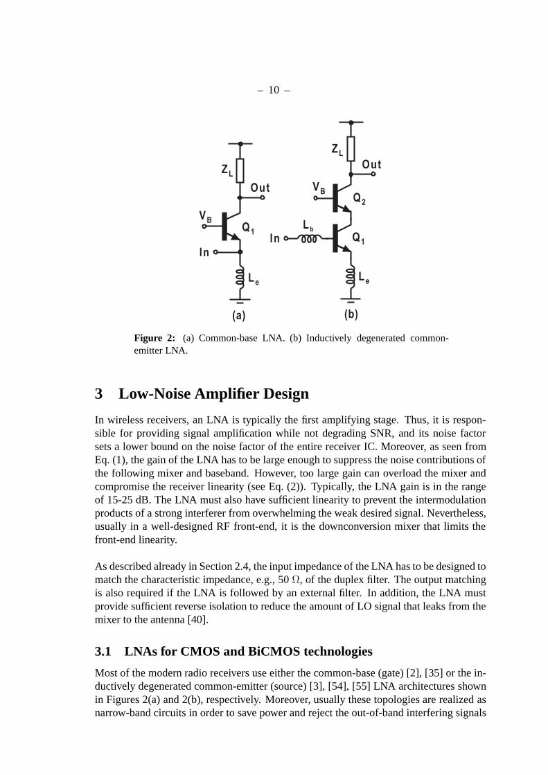
Figure 2: (a) Common-base LNA. (b) Inductively degenerated common-emitter LNA.
3 Low-Noise Amplifier Design
In wireless receivers, an LNA is typically the first amplifying stage. Thus, it is respon-sible for providing signal amplification while not degrading SNR, and its noise factorsets a lower bound on the noise factor of the entire receiver IC. Moreover, as seen fromEq. (1), the gain of the LNA has to be large enough to suppress the noise contributions ofthe following mixer and baseband. However, too large gain can overload the mixer andcompromise the receiver linearity (see Eq. (2)). Typically, the LNA gain is in the rangeof 15-25 dB. The LNA must also have sufficient linearity to prevent the intermodulationproducts of a strong interferer from overwhelming the weak desired signal. Nevertheless,usually in a well-designed RF front-end, it is the downconversion mixer that limits thefront-end linearity.
As described already in Section 2.4, the input impedance of the LNA has to be designed tomatch the characteristic impedance, e.g., 50 Ω, of the duplex filter. The output matchingis also required if the LNA is followed by an external filter. In addition, the LNA mustprovide sufficient reverse isolation to reduce the amount of LO signal that leaks from themixer to the antenna [40].
3.1 LNAs for CMOS and BiCMOS technologies
Most of the modern radio receivers use either the common-base (gate) [2], [35] or the in-ductively degenerated common-emitter (source) [3], [54], [55] LNA architectures shownin Figures 2(a) and 2(b), respectively. Moreover, usually these topologies are realized asnarrow-band circuits in order to save power and reject the out-of-band interfering signals
– 11 –
and noise. Unfortunately, typically the use of common-base and common-gate LNAs islimited only to applications, where the LNA noise figure (NF = 10 log(F )) of 2-3 dB,or above, is tolerable. Nevertheless, a common-base LNA utilizing feedback is capableof achieving NF below 2 dB [56]. Unfortunately, in feedback-type LNAs, the realizationof variable gain (or discrete values of gain) becomes complicated, because the LNA in-put impedance depends on the voltage gain of the amplifier. On the other hand, if thevariable gain is implemented in a mixer instead of an LNA [56], the mixer must havehigher linearity. For these reasons, nowadays, most of the wireless receivers use the in-ductively degenerated common-emitter or common-source LNA architectures. With thesecircuit topologies, excellent input matching and NF below 2 dB can be achieved simul-taneously. For this reason, this thesis concentrates only on the inductively degeneratedcommon-emitter and common-source LNA circuits.
3.2 Impacts of packaging and ESD protection
In consumer electronics applications in which mass production is used, the integratedcircuits are almost always mounted in a package to protect the circuits from being dam-aged. In addition, off-chip interfaces must be protected against ESD. In the circuit designfor RF frequencies, the package and ESD parasitics can have a significant effect on thecircuit performance. Moreover, in general, these parasitics do not scale down with tech-nology [30]. For these reasons, the package and ESD parasitics must be carefully modeledand considered during the circuit design phase, since they are a vital part of the circuit.For the circuit simulations accurate models for the parasitics are preferred, but analyticalmodels are essential to develop guidelines for circuit design and optimization.
Typically, in zero- or low-IF receivers with an on-chip VCO (see Fig. 1), the only RFoff-chip interface is the LNA input. Thus, the package and ESD parasitics have effect onthe RF front-end performance only via the LNA input, as the differential signal processingis considered. Non-ideal ground and supply pins have effect only on the common-modesignals.
Although most of the reported wireless receivers use the common-emitter (source) LNAarchitecture and the optimization of this topology has been extensively examined in theliterature, the effects of the package and ESD parasitics are often for simplicity neglectedin the analysis [54], [55], [57], [58], [59]. However, as the off-chip parasitics are part ofthe LNA, the models for the parasitics are necessary to predict the LNA performance.
In the following, the effects of packaging, parasitics of ESD protection structures, andthe input impedance matching network on the performance of inductively degeneratedcommon-emitter and common-source LNAs are studied and the performance of the pack-aged LNAs are optimized. It is shown that the package and ESD parasitics have effecton the LNA input impedance, input stage transconductance, voltage gain, noise factor,and linearity. The presented equations provide design guidelines and insight for the op-timization principles and fundamental limitations of the packaged common-emitter andcommon-source LNAs.

– 12 –
! "
#
$
% $
&
' # ( )
*
$ +
$
)
, # %
-
. / / / 0 1
2 0 2 /
2 3
Figure 3: (a) Single-ended equivalent circuit of packaged inductively degener-ated common-emitter LNA with ESD protection and (b) its input stage small-signal model.
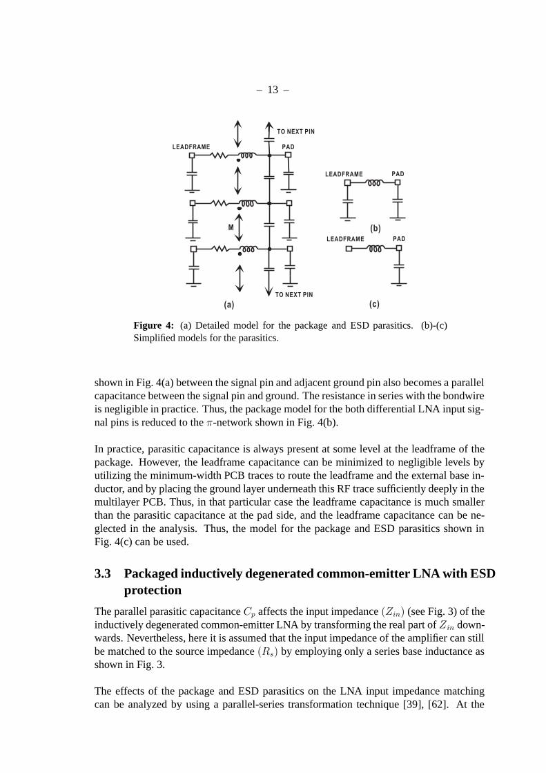
The effects of the package parasitics and ESD protection diodes on the inductively degen-erated common-emitter LNA performance can be analyzed by considering the schematicshown in Fig. 3. Only the single-ended equivalent circuit of the packaged amplifier withESD protection is shown, but the results to be presented apply also to the balanced config-uration. As shown in Fig. 3, the bonding pad, ESD diodes, Miller capacitance of Q1, andparasitic capacitance of bondwire introduce a parallel parasitic capacitance at the base ofthe LNA input device Q1 (see node ’b’ in Fig. 3). The total parasitic capacitance can bemodeled as an equivalent parallel package parasitic capacitance Cp at the base of Q1,as shown in Fig. 3(b) [34], [60], [61], [62], [Paper II], [Paper IV]. In Fig. 3, the effectsof the self inductance of the bondwire and the inductance due to the mutual inductancebetween the adjacent bondwires are modeled by a series inductance Lbw. Since Lbw is inseries with an external matching inductor (Lm), the total series base inductance (Lb) isLm + Lbw. The model for the parasitics shown in Fig. 3 can be made relatively accurateprovided that the adjacent pins of RF signals are grounded or otherwise properly termi-nated, as described in detail below.
Although the model for the package and ESD parasitics shown in Fig. 3 uses only twocircuit elements, it will still give a clear and accurate insight into how the properties of theLNA are modified by the parasitics. Moreover, the model shown is convenient for handcalculation purposes. In simulations, however, a detailed model shown in Fig. 4(a) can beused.
If a balanced LNA topology is employed and the differential input signal pins of theamplifier are selected so that the adjacent pins are ground pins, each coupling capacitance
– 13 –
/ . /
4
/ . /
2
2
2
2
2
2
Figure 4: (a) Detailed model for the package and ESD parasitics. (b)-(c)Simplified models for the parasitics.
shown in Fig. 4(a) between the signal pin and adjacent ground pin also becomes a parallelcapacitance between the signal pin and ground. The resistance in series with the bondwireis negligible in practice. Thus, the package model for the both differential LNA input sig-nal pins is reduced to the π-network shown in Fig. 4(b).
In practice, parasitic capacitance is always present at some level at the leadframe of thepackage. However, the leadframe capacitance can be minimized to negligible levels byutilizing the minimum-width PCB traces to route the leadframe and the external base in-ductor, and by placing the ground layer underneath this RF trace sufficiently deeply in themultilayer PCB. Thus, in that particular case the leadframe capacitance is much smallerthan the parasitic capacitance at the pad side, and the leadframe capacitance can be ne-glected in the analysis. Thus, the model for the package and ESD parasitics shown inFig. 4(c) can be used.
3.3 Packaged inductively degenerated common-emitter LNA with ESDprotection
The parallel parasitic capacitance Cp affects the input impedance (Zin) (see Fig. 3) of theinductively degenerated common-emitter LNA by transforming the real part of Zin down-wards. Nevertheless, here it is assumed that the input impedance of the amplifier can stillbe matched to the source impedance (Rs) by employing only a series base inductance asshown in Fig. 3.
The effects of the package and ESD parasitics on the LNA input impedance matchingcan be analyzed by using a parallel-series transformation technique [39], [62]. At the

– 14 –
operation frequency, the real part of Zin can be approximated by [Paper II]
Re(Zin) = Rin =
(Cπ
Cp + Cπ
)2
· Req = k2 ·Req (3)
where
Req =gmLeCπ
+ rb ≈ ωTLe (4)
and
k =Cπ
Cp + Cπ(5)
Here Req represents the real part of the impedance Zb looking into the base of Q1. More-over, Req is the real part of the LNA input impedance, which is achieved in the absenceof parasitics [32] (i.e. Cp = 0). In addition, the input impedance matching requires thatRin = Rs. Here Le is the emitter inductance, Cπ is the base-emitter capacitance, gm isthe transconductance, rb is the base resistance, and ωT ≈ gm/Cπ is the unity-current gainangular frequency of Q1, respectively. The value of Lb must be selected to tune the inputimpedance to the frequency of interest (f0) [Paper II]
Lb =1
(Cp + Cπ)ω20
(6)
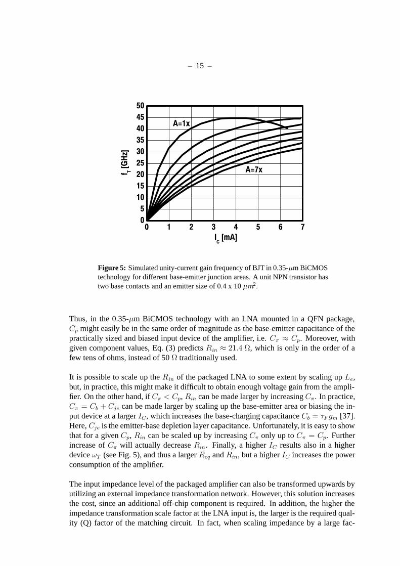
Figure 5 illustrates the simulated fT of a bipolar transistor in a 0.35-µm BiCMOS tech-nology for different base-emitter areas (A = 1, 2, ...7×), and as a function of collectorbias current (IC). The unit NPN transistor has two base contacts and an emitter size of0.4 x 10 µm2. It is seen that, if the base-emitter junction area is increased, for instance, toreduce rb, the BJT has to be biased at a larger IC to obtain a certain fT . The decline infT at high collector currents (clearly seen in Fig. 5 for A = 1) is due to an increase in thebase transit time in the forward direction (τF ) caused by high-level of injection and Kirkeffect at high currents [37].
From Eq. (3) it is concluded that, because of the parasitic capacitance at the transistorbase, the LNA input impedance comes down by a factor of k2 ≤ 1 compared to the un-packaged amplifier with a given ωT and a certain size of Le. Accordingly, in general, toachieve a comparable LNA input impedance level, a packaged amplifier requires a largerLe for a given sized input device (i.e. Cπ) and IC (gm = IC/Vt) than the correspondingunpackaged LNA (i.e. Cp = 0). At 29C, Vt = kBT/q =26mV where q is the electroncharge, kB is the Bolzmann’s constant, and T is absolute temperature, respectively.
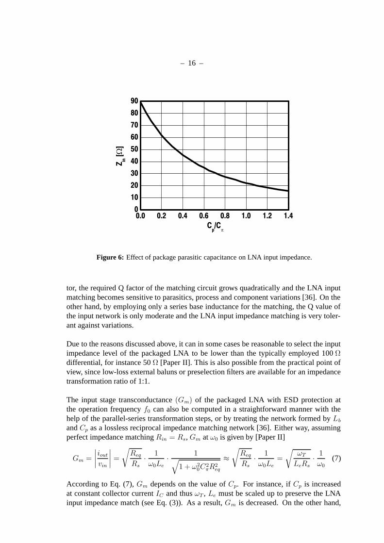
Figure 6 illustrates the effect of Cp on the single-ended LNA input impedance at the reso-nance frequency. In this example, f0=1.575 GHz, Ic = 1.1 mA,Le = 1.1 nH,Cπ = 575 fF,and rb = 5 Ω giving Req ≈ 89 Ω. The values represent rather typical values for the LNAdesigned in a 0.35-µm BiCMOS technology for GPS applications [Paper II]. Moreover,in the 0.35-µm BiCMOS technology utilized in this work, the total parasitic parallel ca-pacitance Cp including the capacitance due to the quad flat nonleaded (QFN) packageparasitics, ESD protection diodes, and bonding pad structure is about 600 fF [Paper II].
– 15 –
Figure 5: Simulated unity-current gain frequency of BJT in 0.35-µm BiCMOStechnology for different base-emitter junction areas. A unit NPN transistor hastwo base contacts and an emitter size of 0.4 x 10 µm2.
Thus, in the 0.35-µm BiCMOS technology with an LNA mounted in a QFN package,Cp might easily be in the same order of magnitude as the base-emitter capacitance of thepractically sized and biased input device of the amplifier, i.e. Cπ ≈ Cp. Moreover, withgiven component values, Eq. (3) predicts Rin ≈ 21.4 Ω, which is only in the order of afew tens of ohms, instead of 50 Ω traditionally used.
It is possible to scale up the Rin of the packaged LNA to some extent by scaling up Le,but, in practice, this might make it difficult to obtain enough voltage gain from the ampli-fier. On the other hand, if Cπ < Cp, Rin can be made larger by increasing Cπ. In practice,Cπ = Cb + Cje can be made larger by scaling up the base-emitter area or biasing the in-put device at a larger IC , which increases the base-charging capacitance Cb = τF gm [37].Here, Cje is the emitter-base depletion layer capacitance. Unfortunately, it is easy to showthat for a given Cp, Rin can be scaled up by increasing Cπ only up to Cπ = Cp. Furtherincrease of Cπ will actually decrease Rin. Finally, a higher IC results also in a higherdevice ωT (see Fig. 5), and thus a larger Req and Rin, but a higher IC increases the powerconsumption of the amplifier.
The input impedance level of the packaged amplifier can also be transformed upwards byutilizing an external impedance transformation network. However, this solution increasesthe cost, since an additional off-chip component is required. In addition, the higher theimpedance transformation scale factor at the LNA input is, the larger is the required qual-ity (Q) factor of the matching circuit. In fact, when scaling impedance by a large fac-
– 16 –
Figure 6: Effect of package parasitic capacitance on LNA input impedance.
tor, the required Q factor of the matching circuit grows quadratically and the LNA inputmatching becomes sensitive to parasitics, process and component variations [36]. On theother hand, by employing only a series base inductance for the matching, the Q value ofthe input network is only moderate and the LNA input impedance matching is very toler-ant against variations.
Due to the reasons discussed above, it can in some cases be reasonable to select the inputimpedance level of the packaged LNA to be lower than the typically employed 100 Ωdifferential, for instance 50 Ω [Paper II]. This is also possible from the practical point ofview, since low-loss external baluns or preselection filters are available for an impedancetransformation ratio of 1:1.
The input stage transconductance (Gm) of the packaged LNA with ESD protection atthe operation frequency f0 can also be computed in a straightforward manner with thehelp of the parallel-series transformation steps, or by treating the network formed by Lband Cp as a lossless reciprocal impedance matching network [36]. Either way, assumingperfect impedance matching Rin = Rs, Gm at ω0 is given by [Paper II]
Gm =
∣∣∣∣ioutvin
∣∣∣∣ =
√ReqRs
· 1
ω0Le· 1√
1 + ω20C
2πR
2eq
≈√ReqRs
· 1
ω0Le=
√ωTLeRs
· 1
ω0
(7)
According to Eq. (7), Gm depends on the value of Cp. For instance, if Cp is increasedat constant collector current IC and thus ωT , Le must be scaled up to preserve the LNAinput impedance match (see Eq. (3)). As a result, Gm is decreased. On the other hand,

– 17 –
in order to preserve both the input impedance and Gm of the amplifier in their originalvalues, both Le and ωT must be scaled up if Cp is increased.
Assuming that the LNA drives I and Q downconversion mixers directly on-chip, as isusual in direct conversion and low-IF receivers, the voltage gain of the packaged ampli-fier can be expressed as [Paper II]
Av = |GmZL(jω0)| ≈√ReqRs
· |ZL(jω0)|ω0Le
(8)
where ZL(jω0) is the LNA load impedance at ω0.
The calculation of the noise factor of the packaged LNA with ESD protection can be sig-nificantly simplified if the impedance ZRs looking into the generator (see Fig. 3) is firsttransformed to the equivalent series impedance at the operation frequency f0. The com-plex conjugate impedance matching requires that ZRs = Z∗
b , where Zb is the impedancelooking into the base of Q1. Accordingly,
ZRs = Z∗b ≈
(ωTLe +
1
jω0Cπ+ jω0Le
)∗≈ ωTLe +
j
ω0Cπ(9)
Thus, by calculating all the noise current contributions at the LNA output current, and byassuming perfect power matching Rin = Rs, it can be shown that the noise factor of thepackaged amplifier at f0 is given by [Paper II]
FLNA=1+Rlbk2Req
+rbReq
+gmReq2β0
+1
2gmReqβ0
(ωTω0
)2+gmReq
2
(ω0
ωT
)2
+4ReqRL
(ω0
ωT
)2(10)
where β0 is the low-frequency current gain of Q1. The first and second terms are thethermal noise due to the series resistance (Rlb) of Lb and rb, respectively. The third andfourth terms account for the shot noise in the base current i2b = 2qIC∆f/β0, the fifth is dueto the shot noise in the collector current i2c = 2qIC∆f , while the last term is the thermalnoise due to the equivalent load resistor (RL). Eq. (10) neglects the noise contribution ofthe cascode transistor to the LNA noise factor. This, however, is a reasonable assumption[Paper II]. Since Req = Rs/k
2, Eq. (10) can also be written as
FLNA = 1 +RlbRs
+rbk
2
Rs+gmRs2β0k2
+k2
2gmRsβ0
(ωTω0
)2+gmRs2k2
(ω0
ωT
)2
+4Rsk2RL
(ω0
ωT
)2
(11)If Eq. (11) is compared with the equation describing the noise factor of the unpackagedLNA [55], it can be seen that, excluding the noise due to Rlb, the equation for the noisefactor of the packaged amplifier is obtained from the unpackaged case by replacing Rs byReq = Rs/k
2. This is also intuitively reasonable, since in packaged LNA, Req representsthe real part of the impedance ZRs looking into the generator at impedance match.
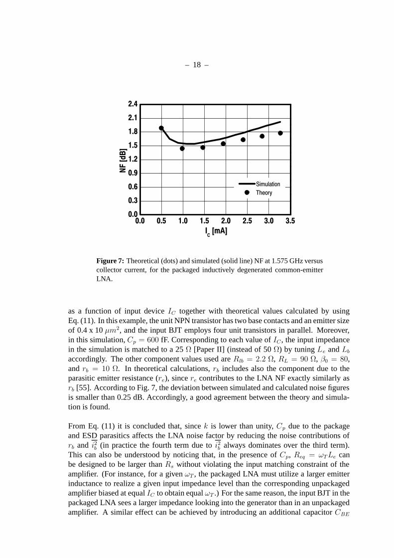
To validate Eq. (11) by means of circuit simulation, Figure 7 plots the simulated NF(10 log(FLNA)) of the packaged LNA in 0.35-µmBiCMOS with ESD protection at 1.575 GHz
– 18 –
Figure 7: Theoretical (dots) and simulated (solid line) NF at 1.575 GHz versuscollector current, for the packaged inductively degenerated common-emitterLNA.
as a function of input device IC together with theoretical values calculated by usingEq. (11). In this example, the unit NPN transistor has two base contacts and an emitter sizeof 0.4 x 10 µm2, and the input BJT employs four unit transistors in parallel. Moreover,in this simulation, Cp = 600 fF. Corresponding to each value of IC , the input impedancein the simulation is matched to a 25 Ω [Paper II] (instead of 50 Ω) by tuning Le and Lbaccordingly. The other component values used are Rlb = 2.2 Ω, RL = 90 Ω, β0 = 80,and rb = 10 Ω. In theoretical calculations, rb includes also the component due to theparasitic emitter resistance (re), since re contributes to the LNA NF exactly similarly asrb [55]. According to Fig. 7, the deviation between simulated and calculated noise figuresis smaller than 0.25 dB. Accordingly, a good agreement between the theory and simula-tion is found.
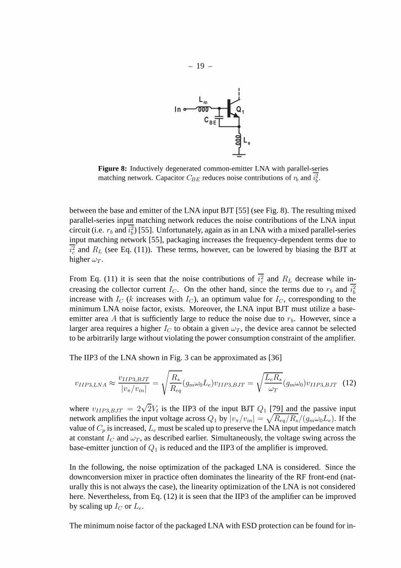
From Eq. (11) it is concluded that, since k is lower than unity, Cp due to the packageand ESD parasitics affects the LNA noise factor by reducing the noise contributions ofrb and i2b (in practice the fourth term due to i2b always dominates over the third term).This can also be understood by noticing that, in the presence of Cp, Req = ωTLe canbe designed to be larger than Rs without violating the input matching constraint of theamplifier. (For instance, for a given ωT , the packaged LNA must utilize a larger emitterinductance to realize a given input impedance level than the corresponding unpackagedamplifier biased at equal IC to obtain equal ωT .) For the same reason, the input BJT in thepackaged LNA sees a larger impedance looking into the generator than in an unpackagedamplifier. A similar effect can be achieved by introducing an additional capacitor CBE
– 19 –
#
"
Figure 8: Inductively degenerated common-emitter LNA with parallel-seriesmatching network. Capacitor CBE reduces noise contributions of rb and i2b .
between the base and emitter of the LNA input BJT [55] (see Fig. 8). The resulting mixedparallel-series input matching network reduces the noise contributions of the LNA inputcircuit (i.e. rb and i2b) [55]. Unfortunately, again as in an LNA with a mixed parallel-seriesinput matching network [55], packaging increases the frequency-dependent terms due toi2c and RL (see Eq. (11)). These terms, however, can be lowered by biasing the BJT athigher ωT .
From Eq. (11) it is seen that the noise contributions of i2c and RL decrease while in-creasing the collector current IC . On the other hand, since the terms due to rb and i2bincrease with IC (k increases with IC), an optimum value for IC , corresponding to theminimum LNA noise factor, exists. Moreover, the LNA input BJT must utilize a base-emitter area A that is sufficiently large to reduce the noise due to rb. However, since alarger area requires a higher IC to obtain a given ωT , the device area cannot be selectedto be arbitrarily large without violating the power consumption constraint of the amplifier.
The IIP3 of the LNA shown in Fig. 3 can be approximated as [36]
vIIP3,LNA ≈ vIIP3,BJT
|vπ/vin| =
√RsReq
(gmω0Le)vIIP3,BJT =
√LeRsωT
(gmω0)vIIP3,BJT (12)
where vIIP3,BJT = 2√
2Vt is the IIP3 of the input BJT Q1 [79] and the passive inputnetwork amplifies the input voltage across Q1 by |vπ/vin| =
√Req/Rs/(gmω0Le). If the
value ofCp is increased, Le must be scaled up to preserve the LNA input impedance matchat constant IC and ωT , as described earlier. Simultaneously, the voltage swing across thebase-emitter junction of Q1 is reduced and the IIP3 of the amplifier is improved.
In the following, the noise optimization of the packaged LNA is considered. Since thedownconversion mixer in practice often dominates the linearity of the RF front-end (nat-urally this is not always the case), the linearity optimization of the LNA is not consideredhere. Nevertheless, from Eq. (12) it is seen that the IIP3 of the amplifier can be improvedby scaling up IC or Le.
The minimum noise factor of the packaged LNA with ESD protection can be found for in-
– 20 –
! "
5 6 !
3
&
& #
2
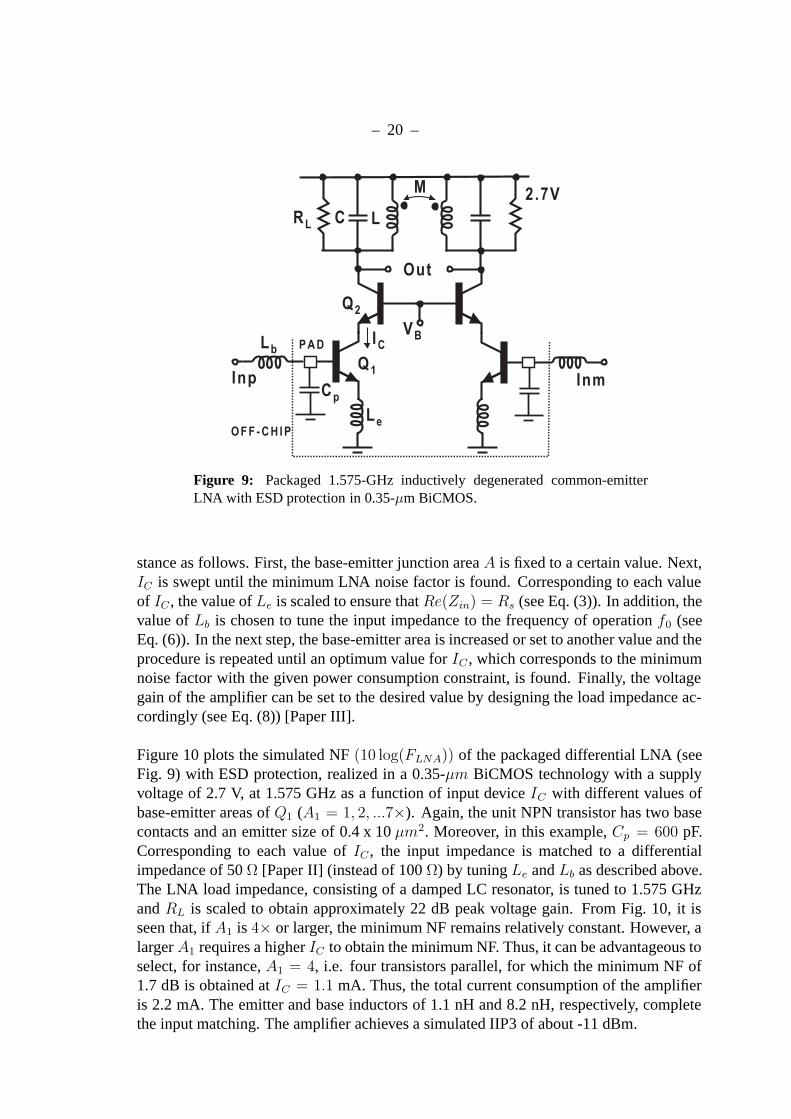
Figure 9: Packaged 1.575-GHz inductively degenerated common-emitterLNA with ESD protection in 0.35-µm BiCMOS.
stance as follows. First, the base-emitter junction area A is fixed to a certain value. Next,IC is swept until the minimum LNA noise factor is found. Corresponding to each valueof IC , the value of Le is scaled to ensure that Re(Zin) = Rs (see Eq. (3)). In addition, thevalue of Lb is chosen to tune the input impedance to the frequency of operation f0 (seeEq. (6)). In the next step, the base-emitter area is increased or set to another value and theprocedure is repeated until an optimum value for IC , which corresponds to the minimumnoise factor with the given power consumption constraint, is found. Finally, the voltagegain of the amplifier can be set to the desired value by designing the load impedance ac-cordingly (see Eq. (8)) [Paper III].
Figure 10 plots the simulated NF (10 log(FLNA)) of the packaged differential LNA (seeFig. 9) with ESD protection, realized in a 0.35-µm BiCMOS technology with a supplyvoltage of 2.7 V, at 1.575 GHz as a function of input device IC with different values ofbase-emitter areas of Q1 (A1 = 1, 2, ...7×). Again, the unit NPN transistor has two basecontacts and an emitter size of 0.4 x 10 µm2. Moreover, in this example, Cp = 600 pF.Corresponding to each value of IC , the input impedance is matched to a differentialimpedance of 50 Ω [Paper II] (instead of 100 Ω) by tuning Le and Lb as described above.The LNA load impedance, consisting of a damped LC resonator, is tuned to 1.575 GHzand RL is scaled to obtain approximately 22 dB peak voltage gain. From Fig. 10, it isseen that, if A1 is 4× or larger, the minimum NF remains relatively constant. However, alarger A1 requires a higher IC to obtain the minimum NF. Thus, it can be advantageous toselect, for instance, A1 = 4, i.e. four transistors parallel, for which the minimum NF of1.7 dB is obtained at IC = 1.1 mA. Thus, the total current consumption of the amplifieris 2.2 mA. The emitter and base inductors of 1.1 nH and 8.2 nH, respectively, completethe input matching. The amplifier achieves a simulated IIP3 of about -11 dBm.

– 21 –
Figure 10: NF of packaged LNA at 1.575 GHz for different input transistorbase-emitter areas.
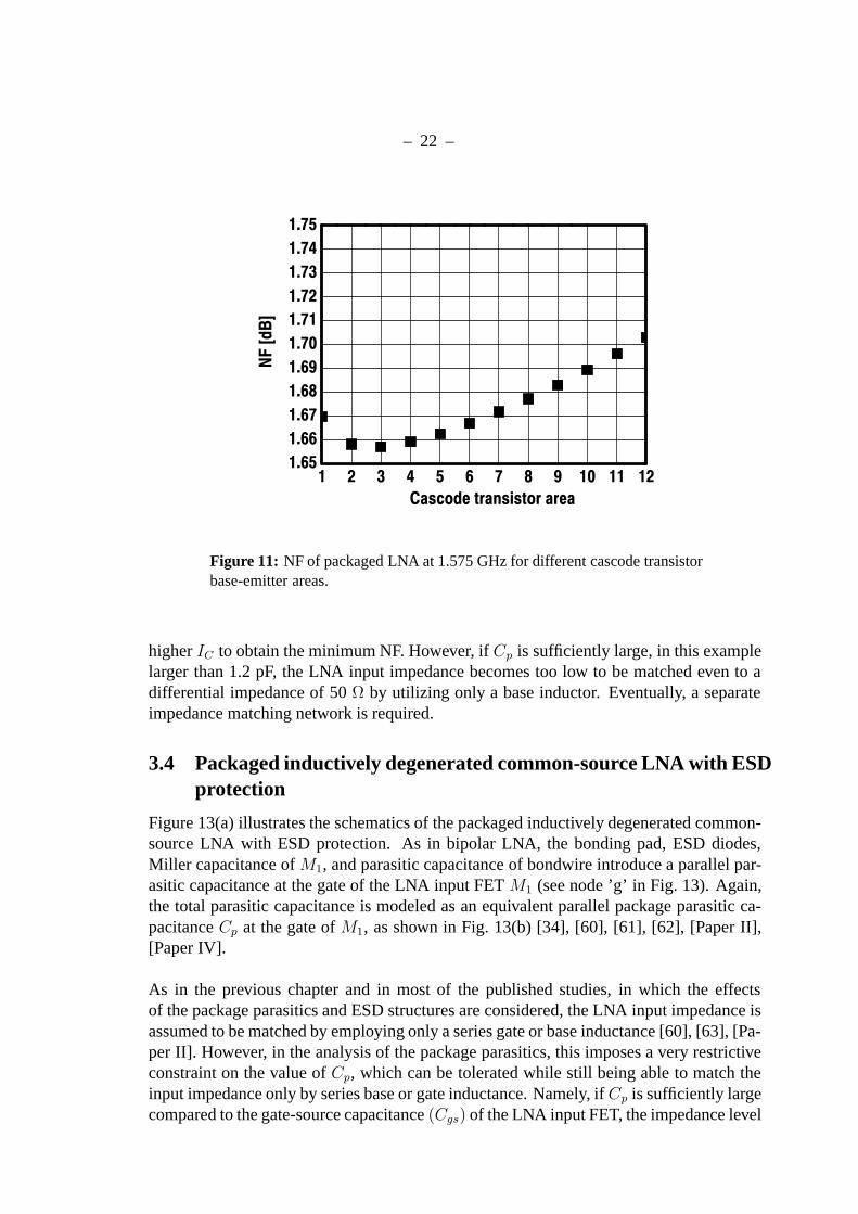
Figure 11 illustrates the simulated NF of the amplifier shown in Fig. 9 at 1.575 GHz as afunction of the cascode transistor area (A2). Here, A1 = 4×, Le = 1.1 nH, Lb = 8.2 nH,and IC = 1.1 mA. It is seen that, in this case, the cascode transistor area has small effecton the LNA NF. In general, however, the noise contribution of the cascode device Q2 isminimized by minimizing the parasitic capacitance at the emitter of Q2.
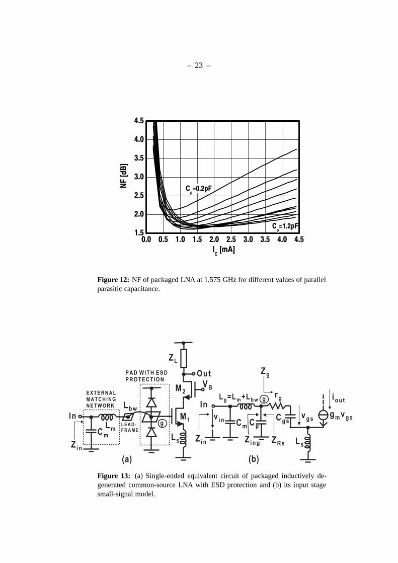
In Fig. 12, the NF of the packaged LNA shown in Fig. 9 is plotted as a function of theinput device IC and with different values of Cp due to the package and ESD structures(Cp = 0.2, 0.3, ...1.2 pF). Again, at each point, the input impedance of the amplifier ismatched to a differential impedance of 50 Ω by tuning Le and Lb accordingly. Moreover,in this example, A1 = 4× and A2 = 1×. From Fig. 12 it is seen that as Cp is increased,the LNA NF is improved first due to the fact that the noise contributions due to rb andi2b are reduced, as also predicted theoretically. Accordingly, Cp reduces the noise due tothe LNA input circuit similarly to a parallel capacitance CBE connected between the baseand emitter of the LNA input BJT [55] (see Fig. 8). In this case, the optimum value of Cpis about 0.7-0.8 pF, which results in NF of 1.6 dB. Nevertheless, if Cp is about 0.5-1.2 pF,the minimum LNA NF remains almost constant (∼1.6-1.7 dB). However, the larger valueof Cp calls for a higher value of IC to obtain the minimum NF. Again, this agrees wellwith theoretical derivations. Since the larger Cp implies a smaller value of k (see Equa-tions (5) and (11)), the larger Cp increases the noise contributions of i2c and RL. However,these noise contributions can be reduced to the original levels by scaling up IC , whichresults in higher values for both k and ωT . As a result, the higher value of Cp requires a
– 22 –
Figure 11: NF of packaged LNA at 1.575 GHz for different cascode transistorbase-emitter areas.
higher IC to obtain the minimum NF. However, if Cp is sufficiently large, in this examplelarger than 1.2 pF, the LNA input impedance becomes too low to be matched even to adifferential impedance of 50 Ω by utilizing only a base inductor. Eventually, a separateimpedance matching network is required.
3.4 Packaged inductively degenerated common-source LNA with ESDprotection
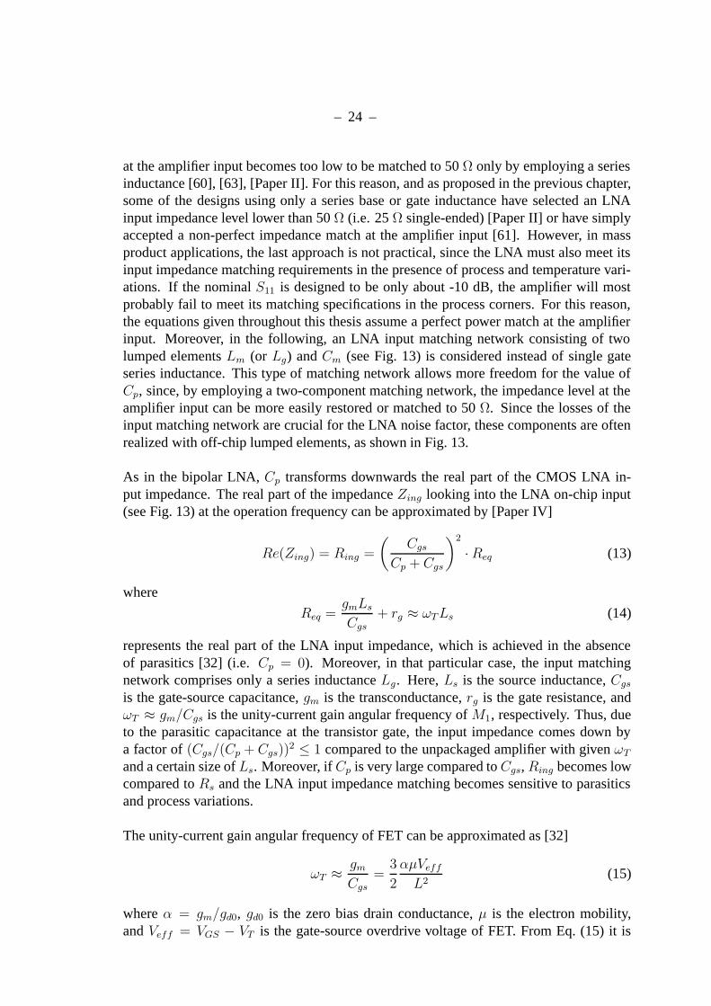
Figure 13(a) illustrates the schematics of the packaged inductively degenerated common-source LNA with ESD protection. As in bipolar LNA, the bonding pad, ESD diodes,Miller capacitance of M1, and parasitic capacitance of bondwire introduce a parallel par-asitic capacitance at the gate of the LNA input FET M1 (see node ’g’ in Fig. 13). Again,the total parasitic capacitance is modeled as an equivalent parallel package parasitic ca-pacitance Cp at the gate of M1, as shown in Fig. 13(b) [34], [60], [61], [62], [Paper II],[Paper IV].
As in the previous chapter and in most of the published studies, in which the effectsof the package parasitics and ESD structures are considered, the LNA input impedance isassumed to be matched by employing only a series gate or base inductance [60], [63], [Pa-per II]. However, in the analysis of the package parasitics, this imposes a very restrictiveconstraint on the value of Cp, which can be tolerated while still being able to match theinput impedance only by series base or gate inductance. Namely, if Cp is sufficiently largecompared to the gate-source capacitance (Cgs) of the LNA input FET, the impedance level
– 23 –
Figure 12: NF of packaged LNA at 1.575 GHz for different values of parallelparasitic capacitance.
! "
$
% $ &
, ' # ( )
-
$ + ,
, # % , -
- $ ,
% , - , -
* ,
#
-
$
,
#
#
)
. / / / 0 1
2 0 2 /
2 3
,
Figure 13: (a) Single-ended equivalent circuit of packaged inductively de-generated common-source LNA with ESD protection and (b) its input stagesmall-signal model.
– 24 –
at the amplifier input becomes too low to be matched to 50 Ω only by employing a seriesinductance [60], [63], [Paper II]. For this reason, and as proposed in the previous chapter,some of the designs using only a series base or gate inductance have selected an LNAinput impedance level lower than 50 Ω (i.e. 25 Ω single-ended) [Paper II] or have simplyaccepted a non-perfect impedance match at the amplifier input [61]. However, in massproduct applications, the last approach is not practical, since the LNA must also meet itsinput impedance matching requirements in the presence of process and temperature vari-ations. If the nominal S11 is designed to be only about -10 dB, the amplifier will mostprobably fail to meet its matching specifications in the process corners. For this reason,the equations given throughout this thesis assume a perfect power match at the amplifierinput. Moreover, in the following, an LNA input matching network consisting of twolumped elements Lm (or Lg) and Cm (see Fig. 13) is considered instead of single gateseries inductance. This type of matching network allows more freedom for the value ofCp, since, by employing a two-component matching network, the impedance level at theamplifier input can be more easily restored or matched to 50 Ω. Since the losses of theinput matching network are crucial for the LNA noise factor, these components are oftenrealized with off-chip lumped elements, as shown in Fig. 13.
As in the bipolar LNA, Cp transforms downwards the real part of the CMOS LNA in-put impedance. The real part of the impedance Zing looking into the LNA on-chip input(see Fig. 13) at the operation frequency can be approximated by [Paper IV]
Re(Zing) = Ring =
(Cgs
Cp + Cgs
)2
·Req (13)
where
Req =gmLsCgs
+ rg ≈ ωTLs (14)
represents the real part of the LNA input impedance, which is achieved in the absenceof parasitics [32] (i.e. Cp = 0). Moreover, in that particular case, the input matchingnetwork comprises only a series inductance Lg. Here, Ls is the source inductance, Cgsis the gate-source capacitance, gm is the transconductance, rg is the gate resistance, andωT ≈ gm/Cgs is the unity-current gain angular frequency of M1, respectively. Thus, dueto the parasitic capacitance at the transistor gate, the input impedance comes down bya factor of (Cgs/(Cp + Cgs))
2 ≤ 1 compared to the unpackaged amplifier with given ωTand a certain size of Ls. Moreover, if Cp is very large compared to Cgs, Ring becomes lowcompared to Rs and the LNA input impedance matching becomes sensitive to parasiticsand process variations.
The unity-current gain angular frequency of FET can be approximated as [32]
ωT ≈ gmCgs
=3
2
αµVeffL2
(15)
where α = gm/gd0, gd0 is the zero bias drain conductance, µ is the electron mobility,and Veff = VGS − VT is the gate-source overdrive voltage of FET. From Eq. (15) it is

– 25 –
Figure 14: Simulated unity-current gain frequency of (W/L) = (60/.13)FET in 0.13-µm CMOS technology.
concluded that the designer can control the fT mainly via VGS and channel length (L).Figure 14 illustrates the simulated fT of FET sized as (W/L) = (60/.13) as a functionof Veff in a 0.13-µm CMOS technology. It is seen that, for the typical overdrive voltagesof 100-200 mV, fT s in the order of 50-70 GHz are available in the 0.13-µm technologyutilized in this thesis. Moreover, since the practical values of Ls are typically in the orderof 1-3 nH, assuming that a 15-25 dB LNA voltage gain is to be implemented (at 2 GHz),the resulting values for Req are in the order of hundreds of ohms (i.e. 300-1300 Ω).
The effect of Cp on Ring is illustrated graphically in Fig. 15. The component valuesused are fT = 65 GHz, Ls = 1.5 nH, and Cgs = 100 fF giving Req = 612 Ω. The valuesrepresent rather typical values for LNA designed in the 0.13-µm CMOS technology forPCS 1900 applications [Paper IV], [Paper VI]. Moreover, in the 0.13-µm CMOS technol-ogy utilized in this work, the total parasitic parallel capacitance including the capacitancedue to the QFN package parasitics, ESD protection diodes, and bonding pad structure isabout 500 fF [Paper II]. (This is almost the same value as Cp = 600 fF in the 0.35-µmBiCMOS technology with a QFN package in the previous chapter. Accordingly, the ESDand package parasitics do not significantly scale down with IC process technology.) Withgiven component values, the resulting Ring is only about 17 Ω. Evidently, if the LNAinput impedance is to be matched to 50 Ω, a matching network is needed to transform theinput impedance of the amplifier upwards.
By applying a series of parallel-series conversions it can be shown that, at the opera-tion frequency f0, the input impedance of the LNA shown in Fig. 13 is given by [Paper
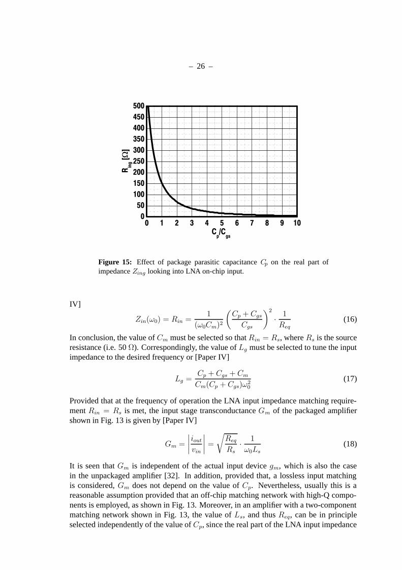
– 26 –
Figure 15: Effect of package parasitic capacitance Cp on the real part ofimpedance Zing looking into LNA on-chip input.
IV]
Zin(ω0) = Rin =1
(ω0Cm)2
(Cp + CgsCgs
)2
· 1
Req(16)
In conclusion, the value of Cm must be selected so that Rin = Rs, where Rs is the sourceresistance (i.e. 50 Ω). Correspondingly, the value of Lg must be selected to tune the inputimpedance to the desired frequency or [Paper IV]
Lg =Cp + Cgs + CmCm(Cp + Cgs)ω
20
(17)
Provided that at the frequency of operation the LNA input impedance matching require-ment Rin = Rs is met, the input stage transconductance Gm of the packaged amplifiershown in Fig. 13 is given by [Paper IV]
Gm =
∣∣∣∣ioutvin
∣∣∣∣ =
√ReqRs
· 1
ω0Ls(18)
It is seen that Gm is independent of the actual input device gm, which is also the casein the unpackaged amplifier [32]. In addition, provided that, a lossless input matchingis considered, Gm does not depend on the value of Cp. Nevertheless, usually this is areasonable assumption provided that an off-chip matching network with high-Q compo-nents is employed, as shown in Fig. 13. Moreover, in an amplifier with a two-componentmatching network shown in Fig. 13, the value of Ls, and thus Req, can be in principleselected independently of the value of Cp, since the real part of the LNA input impedance
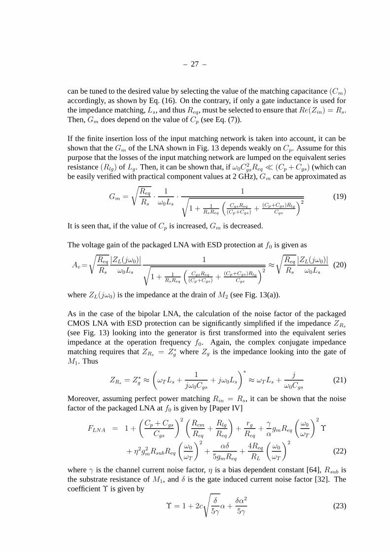
– 27 –
can be tuned to the desired value by selecting the value of the matching capacitance (Cm)accordingly, as shown by Eq. (16). On the contrary, if only a gate inductance is used forthe impedance matching, Ls, and thusReq, must be selected to ensure that Re(Zin) = Rs.Then, Gm does depend on the value of Cp (see Eq. (7)).
If the finite insertion loss of the input matching network is taken into account, it can beshown that the Gm of the LNA shown in Fig. 13 depends weakly on Cp. Assume for thispurpose that the losses of the input matching network are lumped on the equivalent seriesresistance (Rlg) of Lg. Then, it can be shown that, if ω0C
2gsReq (Cp+Cgs) (which can
be easily verified with practical component values at 2 GHz), Gm can be approximated as
Gm =
√ReqRs
· 1
ω0Ls· 1√
1 + 1RsReq
(CgsReq
(Cp+Cgs)+
(Cp+Cgs)Rlg
Cgs
)2(19)
It is seen that, if the value of Cp is increased, Gm is decreased.
The voltage gain of the packaged LNA with ESD protection at f0 is given as
Av=
√ReqRs
|ZL(jω0)|ω0Ls
1√1 + 1
RsReq
(CgsReq
(Cp+Cgs)+
(Cp+Cgs)Rlg
Cgs
)2≈√ReqRs
|ZL(jω0)|ω0Ls
(20)
where ZL(jω0) is the impedance at the drain of M2 (see Fig. 13(a)).
As in the case of the bipolar LNA, the calculation of the noise factor of the packagedCMOS LNA with ESD protection can be significantly simplified if the impedance ZRs
(see Fig. 13) looking into the generator is first transformed into the equivalent seriesimpedance at the operation frequency f0. Again, the complex conjugate impedancematching requires that ZRs = Z∗
g where Zg is the impedance looking into the gate ofM1. Thus
ZRs = Z∗g ≈
(ωTLs +
1
jω0Cgs+ jω0Ls
)∗≈ ωTLs +
j
ω0Cgs(21)
Moreover, assuming perfect power matching Rin = Rs, it can be shown that the noisefactor of the packaged LNA at f0 is given by [Paper IV]
FLNA = 1 +
(Cp + CgsCgs
)2(RcmReq
+RlgReq
)+
rgReq
+γ
αgmReq
(ω0
ωT
)2
Υ
+ η2g2mRsubReq
(ω0
ωT
)2
+αδ
5gmReq+
4ReqRL
(ω0
ωT
)2
(22)
where γ is the channel current noise factor, η is a bias dependent constant [64], Rsub isthe substrate resistance of M1, and δ is the gate induced current noise factor [32]. Thecoefficient Υ is given by
Υ = 1 + 2c
√δ
5γα+
δα2
5γ(23)

– 28 –
where c is the correlation coefficient between the gate and drain noise [32]. In Eq. (22),the first, second, and third terms are the thermal noise produced by the series resistancesRlg and Rcm of the input matching components Lg and Cm, respectively, and rg, respec-tively. The fourth term is due to the channel thermal noise i2d = 4kTγgm∆f , gate-inducedcurrent noise i2g = (4kTδω2
0C2gs∆f)/(5gd0), and correlation between the gate and drain
noise. The fifth and seventh terms are the thermal noise in Rsub and in equivalent loadresistor (RL). Finally, the sixth term is again due to i2g. Eq. (22) neglects the noise contri-bution of the cascode transistor M2 to the LNA noise factor. However, in the following,the noise contribution of M2 is considered separately.
Again, if Eq. (22) is compared to the equation describing the noise factor of the unpack-aged LNA [32], it can be seen that, excluding the noise due to the input matching networkcomponents Rlg and Rcm, the equation for the noise factor of the packaged amplifier isobtained from the unpackaged case by replacing Rs with Req. As in the BJT LNA, this isintuitively reasonable, since in the packaged amplifier, Req represents the real part of theimpedance ZRs looking into the generator at impedance match.
To verify Eq. (22) by means of circuit simulation, Figure 16 plots the simulated NF ofthe packaged LNA in 0.13-µm CMOS with ESD protection at 2 GHz as a function ofinput FET width W together with theoretical values calculated by using Eq. (22). In thissimulation, the input FET employs the channel length of 0.13 µm, the FET is biased atVeff = 200 mV, and the estimated total parasitic capacitance Cp due to the ESD andpackage parasitics is about 500 fF. Corresponding to each value of W , the LNA inputimpedance in the simulation is matched to a 50 Ω by tuning Lm and Cm accordingly.The other component values used are Rcm = 1 Ω, Rlg = 1.5 Ω, Ls = 1.6 nH, andRL = 200 Ω. In addition, parameters γ and δ for a 0.13-µm NMOSFET are estimatedfrom [33] as γ = 1.1 and δ = 4.0, respectively. From Fig. 16 it is concluded that the sim-ulated noise figures fit well with the theoretical ones. At largest, the deviation betweenthe simulated and calculated noise figures is about 0.3 dB.
In the unpackaged LNA (i.e. Cp = 0), the real part of the LNA input impedance isdesigned so that Rin = ωTLs = Rs = 50 Ω. On the other hand, in a packaged amplifierwhere Cp is present, Req is, in practice, designed to be much larger than 50 Ω. Thus, fromEq. (22) it is concluded that, for instance, for given ωT , packaging affects the LNA noisefactor by increasing the noise contributions of the terms proportional to Req, whereasit decreases the noise contributions of terms inversely proportional to Req. Fortunately,very high values of ωT available in sub-micron CMOS processes (i.e. 0.13-µm CMOStechnology utilized in this thesis) suppress the noise contributions proportional toR eq sig-nificantly, since these terms are also inversely proportional to ωT . The noise factor of thepackaged LNA depends directly on Cp only via losses of the input matching network (i.e.Rlg and Rcm). Thus, in practice, in a packaged amplifier the terms proportional to Reqtogether with the losses of the input matching network usually dominate the LNA noisefactor over the rest of the terms inversely proportional to Req.
– 29 –
Figure 16: Theoretical (dots) and simulated (solid line) NF at 2 GHz versusinput FET width, for the packaged inductively degenerated common-sourceLNA.
The IIP3 of the LNA shown in Fig. 13 can be approximated as [36]
vIIP3,LNA ≈ vIIP3,FET
|vgs/vin| =
√RsReq
(gmω0Ls)vIIP3,FET (24)
where vIIP3,FET ≈ 2√
2Veff/(3θ) is the IIP3 of the LNA input FET M1 [Paper V],θ captures how the inversion layer mobility degrades with the gate electric field [2],and the passive matching network amplifies the input voltage across M1 by |vgs/vin| =√Req/Rs/(gmω0Ls).
In the following, the noise optimization of the packaged FET LNA is considered. Again,since the downconversion mixer usually dominates the RF front-end linearity, the linear-ity optimization of the LNA is not considered here. Nevertheless, from Eq. (24) it isseen that the IIP3 of the FET LNA can be scaled up by reducing the voltage gain in thematching network by biasing the FET at larger Veff , scaling up Ls, and by scaling theFET width up. Scaling up the FET channel length also improves the IIP3 of the amplifierby improving the intrinsic FET linearity, since θ is inversely proportional to the channellength.
In modern minimum-sized CMOS devices, the shallow trench isolation (STI) substrateresistance easily dominates over the active area substrate resistance [65] and the substrateresistance is inversely proportional to the device width (W ). On the other hand, the in-put device gm is proportional to W . Thus, from Eq. (22) it is seen that, since the terms
– 30 –
(1 + Cp/Cgs)2 (Rcm +Rlg) /Req and (αδ)/(5gmReq) decrease by increasing W , while
the other terms excluding the noise due toRL increase by increasingW , an optimum inputdevice widthWopt, which minimizes the LNA noise factor, exists, at least in theory. How-ever, the noise due to rg can also be minimized by interdigitating the device [32]. If eachgate finger is contacted at both ends, rg can be approximated as rg = (WRsh)/(12Ln2
f),where nf is the number of gate fingers and Rsh is the sheet resistance of the gate mate-rial [32].
The minimum noise factor of the packaged CMOS LNA with ESD protection can befound, for instance, as follows. First, the minimum, or at least sufficiently low, channellength provided by the given technology is selected to provide high enough ωT given byEq. (15) and to minimize the noise factor given by Eq. (22). Then, the overdrive voltageVeff of the LNA input FET M1 and the value of Ls are set to some arbitrary values. AsVeff and Ls are fixed, Req is also fixed (see Eq. (14)). In the next step, the width Wof M1 is swept until an optimum noise factor is found. Corresponding to each value ofW , the input matching network must be tuned accordingly to ensure that the LNA inputimpedance is matched. Finally, in this phase of the circuit design, it is reasonable to as-sume in the simulations that the cascode FET M2 has the same device width (W2) as M1.
Figure 18 plots the simulated NF (10 log(FLNA)) of the packaged differential LNA withESD protection shown in Fig. 17, realized in the 0.13-µm CMOS technology with a sup-ply voltage of 1.2 V, at 2 GHz with three different values of Veff = 50, 150, 250 mV andas a function of the input FET width (W1). Here L = 0.13 µm, Ls = 1.5 nH, W2 = W1,and at each point the LNA input impedance is matched to a differential impedance of100 Ω. Moreover, in this example, Cp = 500 fF. The LNA load impedance, tuned to2 GHz, is designed to obtain approximately 21 dB peek voltage gain.
From Fig. 18, it is seen that the increase of Veff from 50 mV to 150 mV improves theminimum NF by about 0.2 dB, whereas the increase of Veff from 150 mV to 250 mV doesnot result in NF improvement. Thus, a reasonable choice is Veff = 150 mV. From Fig. 18,it is also concluded that a W1 of 90-150 µm results in the minimum NF correspondingto Veff = 150 mV. However, since the values of 90-150 µm with Veff = 150 mV corre-spond to a relatively high LNA current consumption of 10-14 mA, a slightly lower valueof W1 = 60 µm can be selected instead. This worsens the NF by only 0.2 dB and corre-sponds to the LNA current consumption of 7 mA. In order to minimize the noise contri-butions of rg and Rsub, respectively, the LNA input FET utilizes 10 gate fingers and eachfinger is contacted at both ends. The input matching network consisting of Lg = 7.5 nHand Cmd = 1.5 pF completes the input matching (see Fig. 17). The amplifier achieves anIIP3 of about -5 dBm.
The noise contribution of the LNA cascode FET M2, considering only channel thermalnoise, to the LNA output noise current can be approximated as [Paper V]
i2n,M2=
i2d,M2
1 +(gm2
ω0Cps
)2 ≈(ω0Cpsgm2
)2
4kBTγ
αgm2∆f (25)

– 31 –
! "
-
5 !
3 &
# 7
,
2
Figure 17: Packaged 2-GHz inductively degenerated common-source LNAwith ESD protection in 0.13-µm CMOS.
where gm2 is the transconductance of M2 and Cps is the parasitic capacitance between thedrain of M1 and ground, respectively. Thus, the noise contribution of M2 is minimizedby minimizing the ratio (ω0Cps)/gm2 [66]. To minimize Cps, it is wise to employ theminimum channel length for M2. Moreover, since, in practice, the LNA bias current andthus also the drain-source current of M2 is determined by the optimization of the LNAinput FET M1, the ratio (ω0Cps)/gm2 can be minimized by selecting the width W2 of M2
accordingly. Often, the LNA noise factor is close to the minimum, when M1 and M2
have the same size. Figure 19 illustrates the simulated NF of the LNA shown in Fig. 17at 2 GHz as a function of W2. Here W1 = 60 µm, Ls = 1.5 nH, and Veff = 150 mV.It is seen that for W2 larger than about 30 µm, NF stays relatively constant. Thus, it isreasonable to select, for instance, W2 = W1 = 60 µm.
In the following, the effect of the equivalent parallel package parasitic capacitance Cpon the NF and voltage gain of the LNA shown in Fig. 17 is considered. It is assumed thatthe losses of the input matching network are lumped on the equivalent series resistanceRlg of the series matching inductor Lg (i.e. Rcm = 0 Ω). It is assumed that Rlg = 1.3 Ω.For Lg = 7.5 nH, this corresponds to about Q of 72 at 2 GHz, which represents a rathertypical value for Q of external lumped inductors. Moreover, in the following example,W2 = W1 = 60 µm, Ls = 1.5 nH, and Veff = 150 mV.
Figure 20 illustrates the simulated NF of the packaged LNA, shown in Fig. 17, at 2 GHz,as a function of the value of Cp in two cases. In the first case, an ideal input matchingnetwork with no insertion loss is assumed (i.e. the noise due to R lg is set to zero in thesimulator), while in the second case, the finite insertion loss is considered (i.e. the noisedue to Rlg is considered). Again at each point, the input matching network is tuned ac-
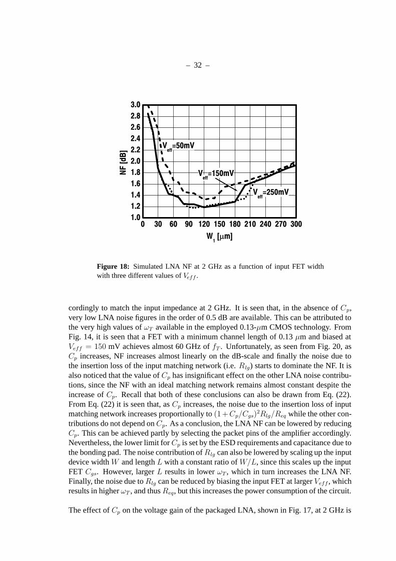
– 32 –
Figure 18: Simulated LNA NF at 2 GHz as a function of input FET widthwith three different values of Veff .
cordingly to match the input impedance at 2 GHz. It is seen that, in the absence of Cp,very low LNA noise figures in the order of 0.5 dB are available. This can be attributed tothe very high values of ωT available in the employed 0.13-µm CMOS technology. FromFig. 14, it is seen that a FET with a minimum channel length of 0.13 µm and biased atVeff = 150 mV achieves almost 60 GHz of fT . Unfortunately, as seen from Fig. 20, asCp increases, NF increases almost linearly on the dB-scale and finally the noise due tothe insertion loss of the input matching network (i.e. Rlg) starts to dominate the NF. It isalso noticed that the value of Cp has insignificant effect on the other LNA noise contribu-tions, since the NF with an ideal matching network remains almost constant despite theincrease of Cp. Recall that both of these conclusions can also be drawn from Eq. (22).From Eq. (22) it is seen that, as Cp increases, the noise due to the insertion loss of inputmatching network increases proportionally to (1+Cp/Cgs)
2Rlg/Req while the other con-tributions do not depend on Cp. As a conclusion, the LNA NF can be lowered by reducingCp. This can be achieved partly by selecting the packet pins of the amplifier accordingly.Nevertheless, the lower limit for Cp is set by the ESD requirements and capacitance due tothe bonding pad. The noise contribution ofRlg can also be lowered by scaling up the inputdevice width W and length L with a constant ratio of W/L, since this scales up the inputFET Cgs. However, larger L results in lower ωT , which in turn increases the LNA NF.Finally, the noise due toRlg can be reduced by biasing the input FET at larger Veff , whichresults in higher ωT , and thusReq, but this increases the power consumption of the circuit.
The effect of Cp on the voltage gain of the packaged LNA, shown in Fig. 17, at 2 GHz is
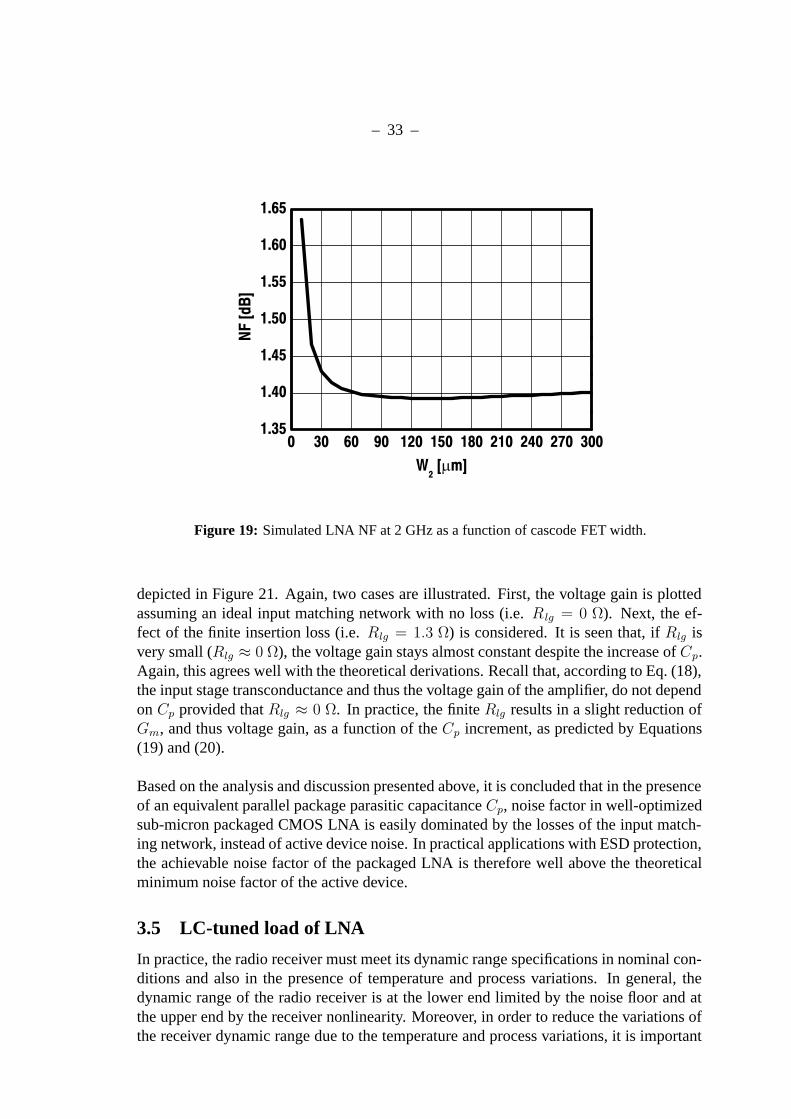
– 33 –
Figure 19: Simulated LNA NF at 2 GHz as a function of cascode FET width.
depicted in Figure 21. Again, two cases are illustrated. First, the voltage gain is plottedassuming an ideal input matching network with no loss (i.e. R lg = 0 Ω). Next, the ef-fect of the finite insertion loss (i.e. Rlg = 1.3 Ω) is considered. It is seen that, if Rlg isvery small (Rlg ≈ 0 Ω), the voltage gain stays almost constant despite the increase of Cp.Again, this agrees well with the theoretical derivations. Recall that, according to Eq. (18),the input stage transconductance and thus the voltage gain of the amplifier, do not dependon Cp provided that Rlg ≈ 0 Ω. In practice, the finite Rlg results in a slight reduction ofGm, and thus voltage gain, as a function of the Cp increment, as predicted by Equations(19) and (20).
Based on the analysis and discussion presented above, it is concluded that in the presenceof an equivalent parallel package parasitic capacitance Cp, noise factor in well-optimizedsub-micron packaged CMOS LNA is easily dominated by the losses of the input match-ing network, instead of active device noise. In practical applications with ESD protection,the achievable noise factor of the packaged LNA is therefore well above the theoreticalminimum noise factor of the active device.
3.5 LC-tuned load of LNA
In practice, the radio receiver must meet its dynamic range specifications in nominal con-ditions and also in the presence of temperature and process variations. In general, thedynamic range of the radio receiver is at the lower end limited by the noise floor and atthe upper end by the receiver nonlinearity. Moreover, in order to reduce the variations ofthe receiver dynamic range due to the temperature and process variations, it is important
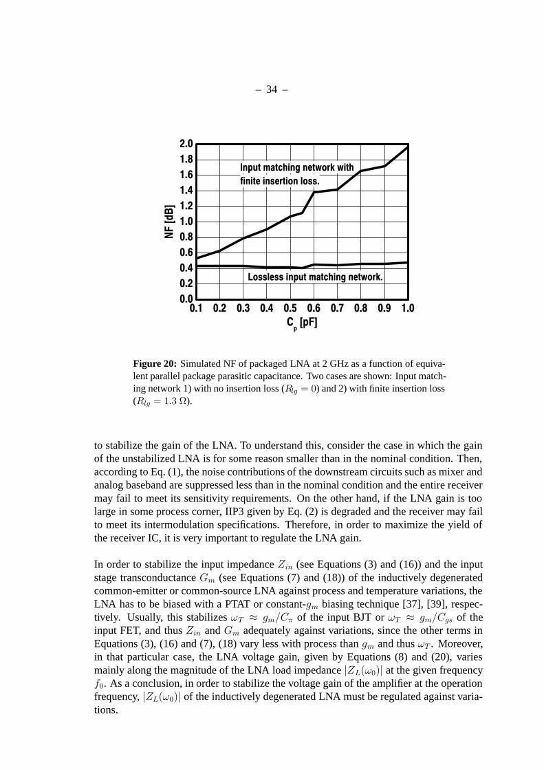
– 34 –
Figure 20: Simulated NF of packaged LNA at 2 GHz as a function of equiva-lent parallel package parasitic capacitance. Two cases are shown: Input match-ing network 1) with no insertion loss (Rlg = 0) and 2) with finite insertion loss(Rlg = 1.3 Ω).
to stabilize the gain of the LNA. To understand this, consider the case in which the gainof the unstabilized LNA is for some reason smaller than in the nominal condition. Then,according to Eq. (1), the noise contributions of the downstream circuits such as mixer andanalog baseband are suppressed less than in the nominal condition and the entire receivermay fail to meet its sensitivity requirements. On the other hand, if the LNA gain is toolarge in some process corner, IIP3 given by Eq. (2) is degraded and the receiver may failto meet its intermodulation specifications. Therefore, in order to maximize the yield ofthe receiver IC, it is very important to regulate the LNA gain.
In order to stabilize the input impedance Zin (see Equations (3) and (16)) and the inputstage transconductance Gm (see Equations (7) and (18)) of the inductively degeneratedcommon-emitter or common-source LNA against process and temperature variations, theLNA has to be biased with a PTAT or constant-gm biasing technique [37], [39], respec-tively. Usually, this stabilizes ωT ≈ gm/Cπ of the input BJT or ωT ≈ gm/Cgs of theinput FET, and thus Zin and Gm adequately against variations, since the other terms inEquations (3), (16) and (7), (18) vary less with process than gm and thus ωT . Moreover,in that particular case, the LNA voltage gain, given by Equations (8) and (20), variesmainly along the magnitude of the LNA load impedance |ZL(ω0)| at the given frequencyf0. As a conclusion, in order to stabilize the voltage gain of the amplifier at the operationfrequency, |ZL(ω0)| of the inductively degenerated LNA must be regulated against varia-tions.

– 35 –
Figure 21: Simulated LNA voltage gain at 2 GHz as a function of equivalentparallel package parasitic capacitance. Two cases are shown: Input matchingnetwork 1) with no insertion loss (Rlg = 0) and 2) with finite insertion loss(Rlg = 1.3 Ω).
Most of the LNAs use an LC-tuned load to peek the gain of the amplifier at the fre-quency of interest and to reject the out-of-band interfering signals. A typical parallel LCcircuit used in narrow-band tuned amplifiers is shown in Fig. 22(a) [3], [Paper I], [PaperII], [Paper VI]. Here C includes also the input capacitances of the I and Q mixers andany other parasitic capacitance presented at the LNA output. The shunt resistor (Rp) low-ers the Q factor of the LC circuit and widens the resonator bandwidth. As a result, themagnitude of the amplifier load impedance varies much less at the operation frequencywith the deviation of C. At the operation frequency f0, L and C are in parallel resonancef0 = 1/(2π
√LC) and ZL is purely real |ZL(ω0)| = RL ≈ (Qindω0L)||roc||Rp ≈ Rp.
Here, Rls is the series resistance of the load inductor L, Qind = (ω0L)/Rls is the Q factorof L, and roc is the output impedance of the cascode amplifier. Unfortunately, as the LNAload impedance at the resonance frequency is mainly determined by Rp, |ZL(ω0)| andalso the LNA voltage gain will deviate similarly as Rp. For instance, with the toleranceof ±20% of integrated polysilicon resistors, the gain variation due to Rp variation only isalmost 20 log 1.2 − 20 log 0.8 =3.5 dB.
A simple technique for regulating the magnitude of an LC-tuned LNA load impedanceat the operation frequency against deviations of both the integrated capacitors and resis-tors is illustrated in Fig. 22(b) [Paper III], [67]. In this circuit, two resistors, Rser andRpar, realized with the same resistance material, are employed to reduce the resonator Q.
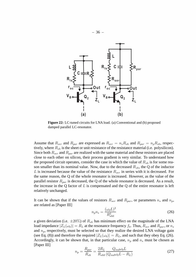
– 36 –
! "
* + 4
8 -
&
! "
* + 4
- *
& *
8 -
Figure 22: LC-tuned circuits for LNA load. (a) Conventional and (b) proposeddamped parallel LC-resonator.
Assume that Rser and Rpar are expressed as Rser = nsRsh and Rpar = npRsh, respec-tively, whereRsh is the sheet or unit resistance of the resistance material (i.e. polysilicon).Since bothRser andRpar are realized with the same material and these resistors are placedclose to each other on silicon, their process gradient is very similar. To understand howthe proposed circuit operates, consider the case in which the value of Rsh is for some rea-son smaller than its nominal value. Now, due to the decreased Rsh, the Q of the inductorL is increased because the value of the resistance Rser in series with it is decreased. Forthe same reason, the Q of the whole resonator is increased. However, as the value of theparallel resistor Rpar is decreased, the Q of the whole resonator is decreased. As a result,the increase in the Q factor of L is compensated and the Q of the entire resonator is leftrelatively unchanged.
It can be shown that if the values of resistors Rser and Rpar, or parameters ns and np,are related as [Paper III]
npns =(ω0L)2
R2sh0
(26)
a given deviation (i.e. ±20%) of Rsh has minimum effect on the magnitude of the LNAload impedance |ZL(ω0)| = RL at the resonance frequency f0. Thus, Rser and Rpar, or nsand np, respectively, must be selected so that they realize the desired LNA voltage gain(see Eq. (8)) and therefore the required |ZL(ω0)| = RL, and such that they obey Eq. (26).Accordingly, it can be shown that, in that particular case, np and ns must be chosen as[Paper III]
np =RparRsh
=2RLRsh0
Qindω0L
(Qindω0L−RL)(27)
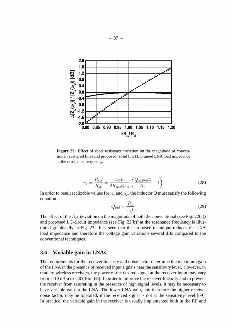
– 37 –
Figure 23: Effect of sheet resistance variation on the magnitude of conven-tional (scattered line) and proposed (solid line) LC-tuned LNA load impedanceat the resonance frequency.
ns =RserRsh
=ω0L
2Rsh0Qind
(Qindω0L
RL− 1
)(28)
In order to result realizable values for ns and np, the inductor Q must satisfy the followingequation
Qind >RLω0L
(29)
The effect of the Rsh deviation on the magnitude of both the conventional (see Fig. 22(a))and proposed LC-circuit impedance (see Fig. 22(b)) at the resonance frequency is illus-trated graphically in Fig. 23. It is seen that the proposed technique reduces the LNAload impedance and therefore the voltage gain variations several dBs compared to theconventional techniques.
3.6 Variable gain in LNAs
The requirements for the receiver linearity and noise factor determine the maximum gainof the LNA in the presence of received input signals near the sensitivity level. However, inmodern wireless receivers, the power of the desired signal at the receiver input may varyfrom -110 dBm to -20 dBm [68]. In order to improve the receiver linearity and to preventthe receiver from saturating in the presence of high signal levels, it may be necessary tohave variable gain in the LNA. The lower LNA gain, and therefore the higher receivernoise factor, may be tolerated, if the received signal is not at the sensitivity level [69].In practice, the variable gain in the receiver is usually implemented both in the RF and
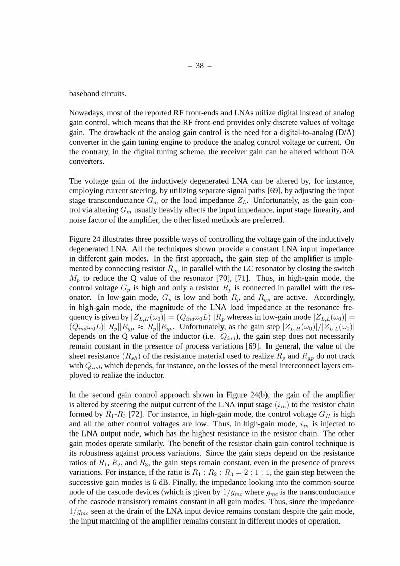
– 38 –
baseband circuits.
Nowadays, most of the reported RF front-ends and LNAs utilize digital instead of analoggain control, which means that the RF front-end provides only discrete values of voltagegain. The drawback of the analog gain control is the need for a digital-to-analog (D/A)converter in the gain tuning engine to produce the analog control voltage or current. Onthe contrary, in the digital tuning scheme, the receiver gain can be altered without D/Aconverters.
The voltage gain of the inductively degenerated LNA can be altered by, for instance,employing current steering, by utilizing separate signal paths [69], by adjusting the inputstage transconductance Gm or the load impedance ZL. Unfortunately, as the gain con-trol via altering Gm usually heavily affects the input impedance, input stage linearity, andnoise factor of the amplifier, the other listed methods are preferred.
Figure 24 illustrates three possible ways of controlling the voltage gain of the inductivelydegenerated LNA. All the techniques shown provide a constant LNA input impedancein different gain modes. In the first approach, the gain step of the amplifier is imple-mented by connecting resistor Rgp in parallel with the LC resonator by closing the switchMp to reduce the Q value of the resonator [70], [71]. Thus, in high-gain mode, thecontrol voltage Gp is high and only a resistor Rp is connected in parallel with the res-onator. In low-gain mode, Gp is low and both Rp and Rgp are active. Accordingly,in high-gain mode, the magnitude of the LNA load impedance at the resonance fre-quency is given by |ZL,H(ω0)| = (Qindω0L)||Rp whereas in low-gain mode |ZL,L(ω0)| =(Qindω0L)||Rp||Rgp ≈ Rp||Rgp. Unfortunately, as the gain step |ZL,H(ω0)|/|ZL,L(ω0)|depends on the Q value of the inductor (i.e. Qind), the gain step does not necessarilyremain constant in the presence of process variations [69]. In general, the value of thesheet resistance (Rsh) of the resistance material used to realize Rp and Rgp do not trackwith Qind, which depends, for instance, on the losses of the metal interconnect layers em-ployed to realize the inductor.
In the second gain control approach shown in Figure 24(b), the gain of the amplifieris altered by steering the output current of the LNA input stage (iin) to the resistor chainformed by R1-R3 [72]. For instance, in high-gain mode, the control voltage GH is highand all the other control voltages are low. Thus, in high-gain mode, iin is injected tothe LNA output node, which has the highest resistance in the resistor chain. The othergain modes operate similarly. The benefit of the resistor-chain gain-control technique isits robustness against process variations. Since the gain steps depend on the resistanceratios of R1, R2, and R3, the gain steps remain constant, even in the presence of processvariations. For instance, if the ratio is R1 : R2 : R3 = 2 : 1 : 1, the gain step between thesuccessive gain modes is 6 dB. Finally, the impedance looking into the common-sourcenode of the cascode devices (which is given by 1/gmc where gmc is the transconductanceof the cascode transistor) remains constant in all gain modes. Thus, since the impedance1/gmc seen at the drain of the LNA input device remains constant despite the gain mode,the input matching of the amplifier remains constant in different modes of operation.
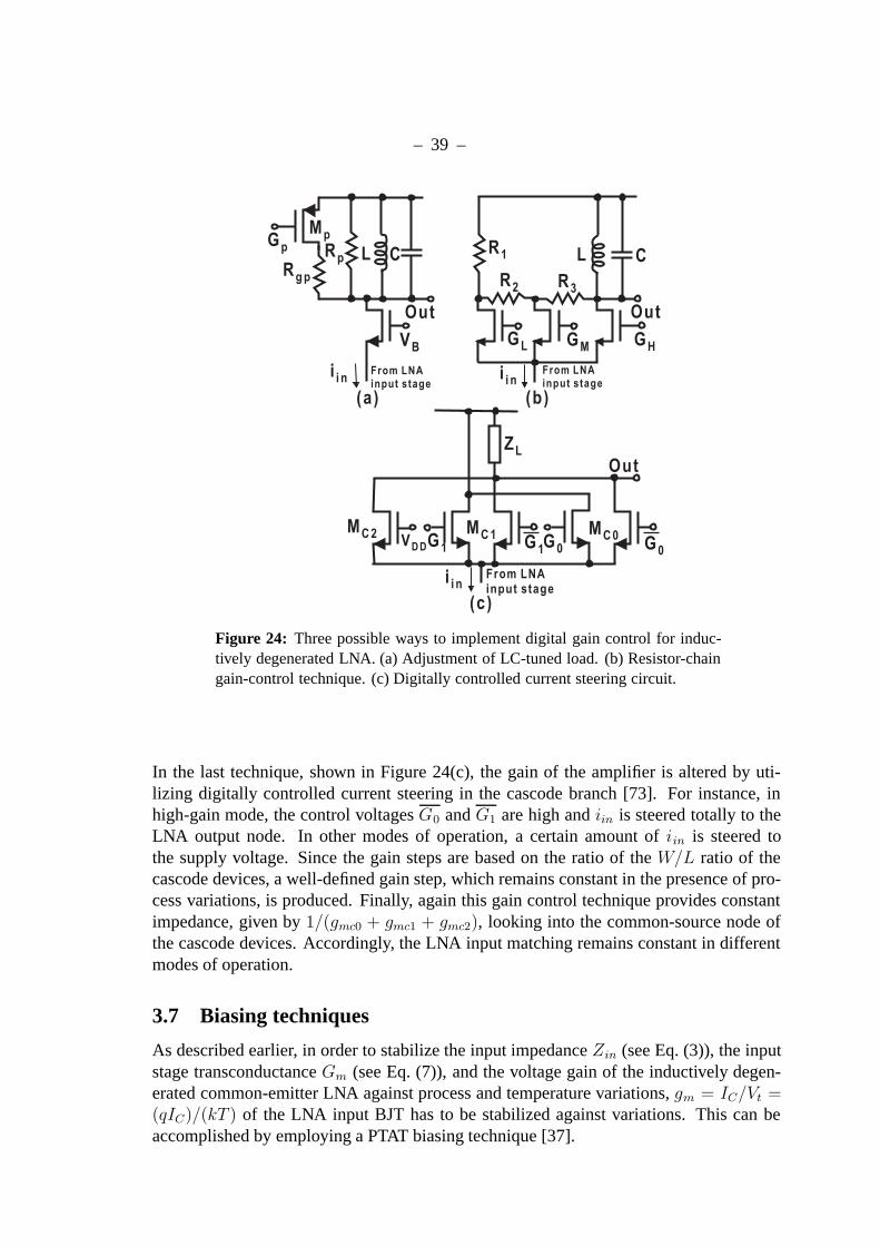
– 39 –
&
&
! "
, &
* + # / $ & - ,
$ $
$ $
4
&
9
$ $ * + # / $ & - ,
* + # / $ & - ,
! 2 2
Figure 24: Three possible ways to implement digital gain control for induc-tively degenerated LNA. (a) Adjustment of LC-tuned load. (b) Resistor-chaingain-control technique. (c) Digitally controlled current steering circuit.
In the last technique, shown in Figure 24(c), the gain of the amplifier is altered by uti-lizing digitally controlled current steering in the cascode branch [73]. For instance, inhigh-gain mode, the control voltages G0 and G1 are high and iin is steered totally to theLNA output node. In other modes of operation, a certain amount of iin is steered tothe supply voltage. Since the gain steps are based on the ratio of the W/L ratio of thecascode devices, a well-defined gain step, which remains constant in the presence of pro-cess variations, is produced. Finally, again this gain control technique provides constantimpedance, given by 1/(gmc0 + gmc1 + gmc2), looking into the common-source node ofthe cascode devices. Accordingly, the LNA input matching remains constant in differentmodes of operation.
3.7 Biasing techniques
As described earlier, in order to stabilize the input impedance Zin (see Eq. (3)), the inputstage transconductance Gm (see Eq. (7)), and the voltage gain of the inductively degen-erated common-emitter LNA against process and temperature variations, gm = IC/Vt =(qIC)/(kT ) of the LNA input BJT has to be stabilized against variations. This can beaccomplished by employing a PTAT biasing technique [37].

– 40 –
" "
*
*
" "
" 9 " :
2 " 2 "
Figure 25: (a) PTAT reference circuit. (b) Constant-gm circuit.
Figure 25(a) illustrates a typical PTAT reference circuit realized in BiCMOS technol-ogy. Although not shown, the bias circuit must use a start-up network to guarantee thatthe circuit ends up in the desired state. The PTAT circuit operates as follows. The NMOSand PMOS current mirrors with current mirror ratios of 1:1 force the collector currentsof QB1 and QB2 to be equal. Therefore, the voltage across the reference resistor (Rref)is the voltage difference between the base-emitter voltages of QB1 and QB2. Thus, thecurrent through Rref is given by
IPTAT =VBE1 − VBE2
Rref=
VtRref
ln
(A2
A1
)=
kT
qRrefln
(A2
A1
)(30)
where A1 and A2 are the base-emitter areas of QB1 and QB2, respectively. Thus, ifthis reference current (IPTAT ) is mirrored by a multiplying factor of M to the collec-tor current of the LNA input device (Q1), gm of Q1 is given by gm = (MIC)/Vt =(M/Rref ) · ln(A2/A1), which is seen to depend only on the geometry and on the value ofRref , as desired.
Similarly, as with a BJT LNA, Zin (see Eq. (16)), Gm (see Eq. (18)), and the voltagegain of the inductively degenerated common-source LNA can be regulated against pro-cess and temperature variations by stabilizing gm of the LNA input FET against variations.In CMOS technology, this can be achieved by utilizing a constant-gm biasing method [39].
One possible way to realize the constant-gm circuit is shown in Figure 25(b) [39]. Again,the start-up network is omitted. If the FET is modeled with its square-law relationship
iDS =µCox
2
W
L(vGS − VT )
2 =K
2
W
L(vGS − VT )
2 (31)

– 41 –
and the sizes of the transistors MB1 − MB4 are chosen as (W/L)B1 = (W/L)B2 =(W/L)B3 = (W/L) and (W/L)B4 = S · (W/L), the drain-source currents of MB1 andMB2 are given as
IDSB1 = IDSB2 =L
KWR2ref
(√S − 1√S
)2
(32)
Accordingly, the transconductance of MB1 and MB2 is
gmB1 = gmB2 =
√2
Rref
(√S − 1√S
)(33)
Thus, for instance, by biasing the LNA input FET by the gate-source voltage of MB1 andMB2, the gm of the LNA input FET can be made to depend only on the geometry and onthe value of Rref .
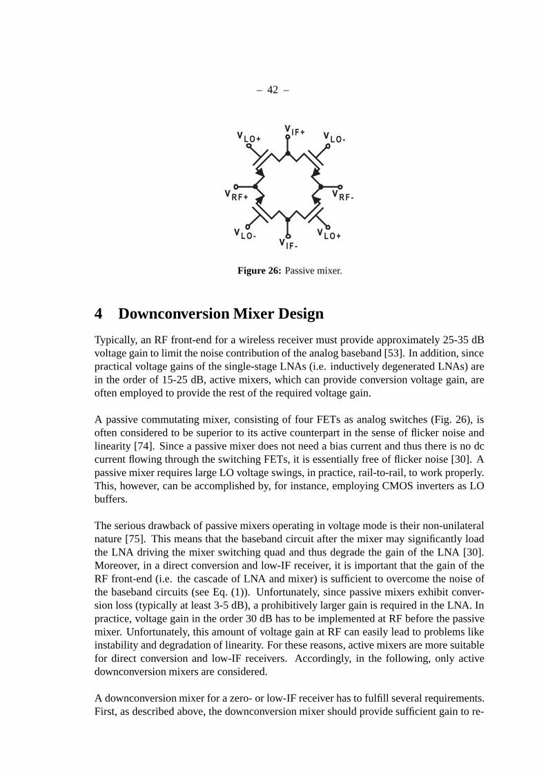
– 42 –
% (
% (
% 3
% 3
% (
% (% 3
% 3
Figure 26: Passive mixer.
4 Downconversion Mixer Design
Typically, an RF front-end for a wireless receiver must provide approximately 25-35 dBvoltage gain to limit the noise contribution of the analog baseband [53]. In addition, sincepractical voltage gains of the single-stage LNAs (i.e. inductively degenerated LNAs) arein the order of 15-25 dB, active mixers, which can provide conversion voltage gain, areoften employed to provide the rest of the required voltage gain.
A passive commutating mixer, consisting of four FETs as analog switches (Fig. 26), isoften considered to be superior to its active counterpart in the sense of flicker noise andlinearity [74]. Since a passive mixer does not need a bias current and thus there is no dccurrent flowing through the switching FETs, it is essentially free of flicker noise [30]. Apassive mixer requires large LO voltage swings, in practice, rail-to-rail, to work properly.This, however, can be accomplished by, for instance, employing CMOS inverters as LObuffers.
The serious drawback of passive mixers operating in voltage mode is their non-unilateralnature [75]. This means that the baseband circuit after the mixer may significantly loadthe LNA driving the mixer switching quad and thus degrade the gain of the LNA [30].Moreover, in a direct conversion and low-IF receiver, it is important that the gain of theRF front-end (i.e. the cascade of LNA and mixer) is sufficient to overcome the noise ofthe baseband circuits (see Eq. (1)). Unfortunately, since passive mixers exhibit conver-sion loss (typically at least 3-5 dB), a prohibitively larger gain is required in the LNA. Inpractice, voltage gain in the order 30 dB has to be implemented at RF before the passivemixer. Unfortunately, this amount of voltage gain at RF can easily lead to problems likeinstability and degradation of linearity. For these reasons, active mixers are more suitablefor direct conversion and low-IF receivers. Accordingly, in the following, only activedownconversion mixers are considered.
A downconversion mixer for a zero- or low-IF receiver has to fulfill several requirements.First, as described above, the downconversion mixer should provide sufficient gain to re-
– 43 –
duce the noise contribution of the analog baseband circuits [76]. Next, a mixer with a lownoise factor is desirable to relax the LNA gain requirement. Notice also that, in general,if the LNA gain can be reduced, the receiver linearity can be improved (see Eq. (2)).
A downconversion mixer aliases both the main and image responses at the output. Ac-cordingly, this must be considered when the mixer noise factor is specified and the noiseis referred to the mixer input. If the mixer output noise is referred to one or both inputsidebands, the single-sideband (SSB) noise factor or double-sideband (DSB) noise factoris considered, respectively. The SSB noise factor is applicable to the superheterodynereceiver, in which only one of the input sidebands (i.e. the RF band) is converted to theIF and the image band is rejected [76]. On the other hand, in a direct conversion receiver,the LO signal is centered in the desired channel. Thus, both the desired signal energyand noise occupy both upper and lower sidebands, and there is no idle sideband to befiltered [2]. Moreover, since the direct conversion receiver keeps the images of signaland noise in separate quadrature channels, the DSB noise factor is applicable to zero-IFarchitecture [46].
Often, in a well-designed RF front-end, the mixer linearity dominates the entire front-endlinearity. In a downconversion mixer, third-order intermodulation (IM3) may cause twolarge adjacent-channel signals to generate IM3 products at spurious frequencies coinci-dent with a weak desired channel. Accordingly, the IIP3 of the mixer has to be sufficientlyhigh to mitigate against this effect. In addition to IIP3, the downconversion mixer for azero- or low-IF receiver has to have adequate ICP to tolerate large blocking or interferencesignals, which may reduce the front-end small-signal gain or increase the noise factor.
If two strong signals at the frequencies of f1 and f2, which are located at the passbandof the preselection filter of the receiver, are exposed to a second-order nonlinearity, un-wanted spurious baseband responses are generated. These are the dc offset componentand the baseband IM2 component at f1 − f2 [77]. In the RF front-end, this may happenboth in the LNA or in the mixer. However, if the LNA and mixer are ac-coupled (which isa common practice), the dc offset and low-frequency beat signal generated in the LNA arefiltered out. Therefore, it is the downconversion mixer that usually determines the achiev-able IIP2 of the entire receiver [28]. Thus, a downconversion mixer with high IIP2 isrequired to protect a zero- or low-IF receiver from unwanted dc offsets and IM2 products,and to minimize the effect of the second-order nonlinearity on the receiver performance.
The mixers utilized in integrated homodyne or low-IF receivers are practically alwaysbased either on single- or double-balanced circuit topologies [42]. If a mixer operates witha differential LO signal and single-ended RF signal, it is called single-balanced. However,if a mixer accommodates both differential RF and LO signals, it is called double-balanced.The double-balanced configurations generate less even-order distortion and provide bet-ter port-to-port isolation than the single-balanced mixers. In addition, the single-balancedtopologies are more susceptible to noise in LO signal [40]. For these reasons, this thesisconcentrates only on double-balanced topologies.
– 44 –
In the following, the design and optimization of bipolar and BiCMOS active downcon-version mixers is discussed first. Next, low-voltage circuit design techniques for CMOSmixers are presented. Then, methods and techniques for suppressing IM2 distortion inmixer RF input stages are discussed and the benefits and drawbacks of different tech-niques are analyzed. It should be noticed that in order to maximize the mixer IIP2 and tominimize the IIP2 sensitivity to mismatches, it is important to minimize the level of thecommon-mode IM2 components in the output current of the mixer RF transconductor.Finally, the characteristics of different RF transconductors are compared both in terms ofIIP2 and IIP3.
The purpose of the following discussion is to provide design guidelines and insight intothe design and optimization principles of active downconversion mixers and the whole RFfront-end. As already mentioned, in practice, the mixer IIP3 often limits the RF front-endlinearity and the mixer IIP2 determines the IIP2 of the entire zero- or low-IF receiver.Finally, since the mixer in practice is preceded only by 15-25 dB voltage gain in the LNA(limited by the receiver linearity requirements), the effect of the mixer noise to the re-ceiver noise is not usually negligible. Thus, besides of the mixer linearity, circuit andoptimization techniques must be utilized to minimize mixer noise.
4.1 Bipolar and BiCMOS downconversion mixers
Most of the active double-balanced mixers utilized in wireless receivers are based on theGilbert mixer topology shown in Fig. 27 [78]. The Gilbert mixer employs a differentialpairQ1-Q2 as its RF input transconductance stage to convert the differential voltage-modeRF signal to a differential current. The current-mode RF signal is then fed through thecurrent-steering cell Q3-Q6 driven by the LO signal. The IF output is also produced asa current-mode and is converted to the voltage at the IF load RL1-RL2. If instantaneousswitching of the switching quad is assumed (i.e. that the current-mode RF signal is mul-tiplied by the square wave toggling at the LO frequency), the mixer voltage conversiongain is given by [30]
Av =2
πgmRL (34)
where gm is the transconductance of Q1 (and Q2). Often, the load of the mixer consists ofa first-order RC low-pass filter (i.e. of a capacitor in parallel with a load resistor), whichimproves the mixer out-of-band blocking characteristics and relaxes the linearity require-ments of the following baseband circuits.
The noise and linearity of the mixer RF input stage are crucial to the mixer performance.Often the linearity of the Gilbert mixer is mainly determined by the RF input stage andis quite poor in the basic Gilbert mixer due to the limitations in the linearity of the BJTdifferential pair [78]. If the bipolar transistor is modeled with its exponential relationship
iC = ISevBE
Vt (35)

– 45 –
% (
9 : ; <
% 3
% (% 3
% (
% 3 % 3 (
Figure 27: Gilbert mixer.
where IS is the collector saturation current and the differential pair is biased by a tailcurrent IT = 2A · IB, the IIP3 of the differential pair can be approximated as [79]
vIIP3 = 4Vt (36)
which represents the differential RF input amplitude. Thus, the IIP3 of the BJT differ-ential pair is fixed approximately to a value of vIIP3 = 4 × 26 mV=104 mV at roomtemperature [79]. The linearity of the RF input stage can be improved by, for example,utilizing an inductive or resistive emitter degeneration [80]. Inductive degeneration resultsin lower noise than resistive degeneration, but, unfortunately, it increases silicon area andcost significantly, because, in I and Q mixers four integrated inductors (or two differen-tial inductors) are required. With resistive degeneration, the IIP3 of the differential pairimproves to [79]
vIIP3 = 4Vt(1 + gmRE)3/2 (37)
where gm = (AIB)/Vt, RE is the emitter degeneration resistance, and gmRE is the loopgain of the negative feedback.
As supply voltage scales down with transistor technology, the stacking of four devices ina standard Gilbert cell becomes difficult or even impossible. For this reason, the Gilbertmixer is often implemented without the tail current source, as shown in Fig. 28. In thiscase, the IIP3 of the mixer can be approximated by assuming that the mixer linearity isdominated by the linearity of the resistively degenerated common-emitter RF input stage,for which the IIP3 can be approximated as [79]
vIIP3 = 4√
2Vt(1 + gmRE)2√|1 − 2gmRE|
(38)
– 46 –
2
% (
9 : ; <
% 3
% (
% 3
% (
% 3 % 3 (
"
0
Figure 28: Resistively degenerated Gilbert mixer without the tail currentsource.
The IIP3 of the degenerated common-emitter RF transconductor is higher by a factor of√2(1 + gmRE)/|1 − 2gmRE| than the corresponding IIP3 of the degenerated differential
pair given by Eq. (37). The drawback of the common-emitter RF input stage is its inabil-ity to reject common-mode interference and its IM2 characteristics, as will be shown inChapter 4.3.1.
In the following, the properties of the downconversion mixer shown in Fig. 28 are ana-lyzed in more detail and the design flow and optimization of the mixer are considered. Inthe mixer shown in Fig. 28, resistorsRCM and RLD determine the mixer output common-mode level and conversion gain, respectively. In addition, current boosting by a currentsource (IB) is employed to relax low-voltage operation [70]. By current boosting, higherconversion voltage gain can be achieved, since larger resistors can be utilized at the out-put, and a lower mixer noise factor is achievable without sacrificing the mixer third-ordernonlinearity.
As the current conversion loss through the switching quad Q3-Q6 is theoretically 2/π,it is easy to show that the voltage conversion gain of the mixer shown in Fig. 28 can beapproximated as
Av =2
π
gm1 + gmRE
RL. (39)
where RL is the equivalent load resistor of the mixer. Moreover, as the conversion gaindepends on gm = IC/VT of Q1, the mixer has to be biased by using the PTAT current [37]
IC =kT
qRreflnA (40)

– 47 –
in order to compensate the temperature variations of the gain. In addition, if RL and REare realized by using the same material as the reference resistance Rref , the mixer gain isin a first-order approximation independent of the process or temperature variations of theresistance material. This type of biasing arrangement stabilizes the gain against supply,temperature, and process variations and therefore guarantees very robust performance.
The DSB noise factor of the downconversion mixer shown in Fig. 28 can be estimatedby considering the noise due to the mixer RF input transconductance stage, load, andswitches. The noise factor is calculated by finding separately all the noise voltage con-tributions at the mixer output. Only white noise is considered, since, in practice, in adownconversion mixer with BJT switches, the flicker noise is not usually an issue, evenin a direct conversion receiver for narrow-band applications, such as GSM.
First, the expressions for the different contributions to the output noise current of theRF input stage are derived. By applying a straightforward circuit analysis, it is easy toshow that the total noise current at the RF differential transconductor output is given by
i2on,gm = 2 × (i2n,Rs+ i2n,rb + i2n,ib + v2
n,ic+ i2n,RE
)
=2 ×
(g2mv
2s + g2
mv2b + g2
m(Rs +RE)2i2b + i2c + g2mR
2Ei
2E
)(1 + gmRE)2 (41)
where the factor of two accounts for the differential operation and i2n,Rs, i2n,rb , i
2n,ib
, i2n,ic ,
and i2n,RErepresent the noise contributions of the source resistance Rs, base resistance rb,
base shot noise ib, collector shot noise ic, and RE , respectively. In addition, here v2s =
4kTRs∆f , v2b = 4kTrb∆f , i2b = 2qIC∆f/β0, i2c = 2qIC∆f , and i2E = 4kT∆f/RE.
If the mixer commutation is assumed square-wave like, the LO frequency and its oddharmonics will downconvert the components of the RF input stage white noise i2on,gm tothe IF frequency. Therefore, the corresponding noise voltage components at the IF aregiven by [41]
v2on,gm = n×
(2
πRL
)2
i2on,gm (42)
where the factor n represents accumulated noise after aliasing. For the harmonic ampli-tudes of the square wave n = π2/4.
The mixer output noise voltage due to the white noise in the four switches Q3-Q6 in adouble-balanced mixer can be approximated as [41]
v2on,sw = 4 × 2kT
R2LISWπALO
∆f (43)
where ALO is the LO amplitude and ISW is the bias current of the switching pair (in amixer with current boosting, ISW is different from the IC of the gm-stage). Eq. (43) isderived by considering only switch collector shot noise.
– 48 –
The output noise voltage due to the equivalent load resistors (RL) is given by
v2on,RL
= 2 × 4kTRL∆f (44)
where the factor of two is due to the two load resistors in the mixer.
The DSB noise factor for a downconversion mixer can be written as
FDSB =v2on
v2on,Rs
=v2on,gm + v2
on,sw + v2on,RL
v2on,Rs
(45)
where v2on is the total mixer output noise and v2
on,Rsis the output noise due to the noise
of the source resistance Rs at the main and image band [81]. The downconverted outputnoise voltage due to the noise of Rs at the main and image band is given by
v2on,Rs
= 2 ×(
2
πRL
)2
2i2n,Rs= 4
(2
πRL
)2g2mv
2s
(1 + gmRE)2 (46)
where the first factor of two is due to the assumption that the mixer conversion gain isequal for both main and image bands. The second factor of two takes into account thenoise in the differential source resistor (2Rs).
By combining the equations derived above, the DSB noise factor can be written as
FDSB=π2
8
(1+
rbRs
+gm(Rs+RE)2
2Rsβ0
+1
2gmRs+RERs
+ISW (1+gmRE)2
g2mRsπALO
+(1+gmRE)2
g2mRLRs
)(47)
From Eq. (47), it is seen that, in order to reduce the noise contributions of the RF in-put transistors Q1-Q2, sufficiently large base-emitter area devices with small rb should beused. Moreover, since all terms involving gm, excluding the term due to the base shotnoise, decrease with IC , the noise factor of the mixer decreases with practical values ofIC . The value of RE should be minimized to maximize the gain of the RF transconductorstage and to minimize the noise contributions of the switching transistors and load. How-ever, since the decrease of RE reduces the loop gain of the negative feedback, the IIP3 ofthe mixer decreases accordingly (see Eq. (38)). Finally, the white noise due to the switch-ing quad Q3-Q6 can be reduced by biasing the switching transistors at lower collectorcurrent ISW and by utilizing LO swing with a sufficiently large amplitude A. However,ISW can not be arbitrary low, because, otherwise, the linearity of the switches is deterio-rated. In addition, a very large LO amplitude results in excessive current being pumpedinto to the common-emitter node of the switching quad through the base-emitter junctioncapacitance (Cje). Thus, additional third-order intermodulation is generated [76].
Figures 29 and 30 plot the simulated IIP3 and DSB-NF (10 log(FDSB)) of the direct con-version downconversion mixer shown in Fig. 28, realized in a 0.35-µm BiCMOS technol-ogy with a supply voltage of 2.7 V, at 2 GHz, as a function of the RF input BJT collector
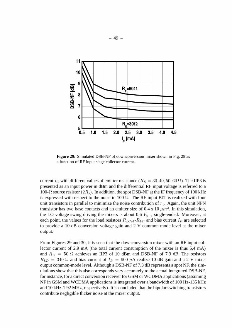
– 49 –
Figure 29: Simulated DSB-NF of downconversion mixer shown in Fig. 28 asa function of RF input stage collector current.
current IC with different values of emitter resistance (RE = 30, 40, 50, 60 Ω). The IIP3 ispresented as an input power in dBm and the differential RF input voltage is referred to a100-Ω source resistor (2Rs). In addition, the spot DSB-NF at the IF frequency of 100 kHzis expressed with respect to the noise in 100 Ω. The RF input BJT is realized with fourunit transistors in parallel to minimize the noise contribution of rb. Again, the unit NPNtransistor has two base contacts and an emitter size of 0.4 x 10 µm2. In this simulation,the LO voltage swing driving the mixers is about 0.6 Vp−p single-ended. Moreover, ateach point, the values for the load resistors RLCM -RLD and bias current IB are selectedto provide a 10-dB conversion voltage gain and 2-V common-mode level at the mixeroutput.
From Figures 29 and 30, it is seen that the downconversion mixer with an RF input col-lector current of 2.9 mA (the total current consumption of the mixer is thus 5.4 mA)and RE = 50 Ω achieves an IIP3 of 10 dBm and DSB-NF of 7.3 dB. The resistorsRLD = 340 Ω and bias current of IB = 900 µA realize 10-dB gain and a 2-V mixeroutput common-mode level. Although a DSB-NF of 7.3 dB represents a spot NF, the sim-ulations show that this also corresponds very accurately to the actual integrated DSB-NF,for instance, for a direct conversion receiver for GSM or WCDMA applications (assumingNF in GSM and WCDMA applications is integrated over a bandwidth of 100 Hz-135 kHzand 10 kHz-1.92 MHz, respectively). It is concluded that the bipolar switching transistorscontribute negligible flicker noise at the mixer output.
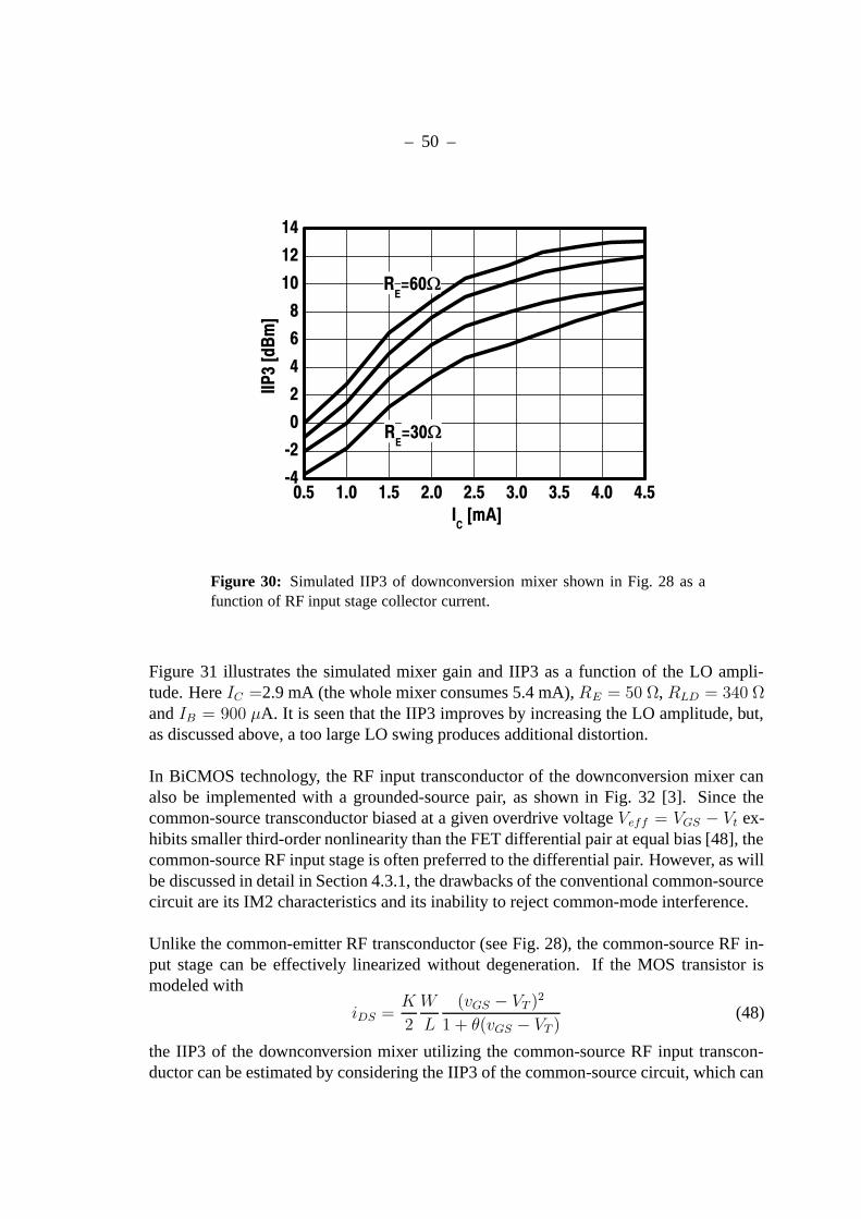
– 50 –
Figure 30: Simulated IIP3 of downconversion mixer shown in Fig. 28 as afunction of RF input stage collector current.
Figure 31 illustrates the simulated mixer gain and IIP3 as a function of the LO ampli-tude. Here IC =2.9 mA (the whole mixer consumes 5.4 mA), RE = 50 Ω, RLD = 340 Ωand IB = 900 µA. It is seen that the IIP3 improves by increasing the LO amplitude, but,as discussed above, a too large LO swing produces additional distortion.
In BiCMOS technology, the RF input transconductor of the downconversion mixer canalso be implemented with a grounded-source pair, as shown in Fig. 32 [3]. Since thecommon-source transconductor biased at a given overdrive voltage Veff = VGS − Vt ex-hibits smaller third-order nonlinearity than the FET differential pair at equal bias [48], thecommon-source RF input stage is often preferred to the differential pair. However, as willbe discussed in detail in Section 4.3.1, the drawbacks of the conventional common-sourcecircuit are its IM2 characteristics and its inability to reject common-mode interference.
Unlike the common-emitter RF transconductor (see Fig. 28), the common-source RF in-put stage can be effectively linearized without degeneration. If the MOS transistor ismodeled with
iDS =K
2
W
L
(vGS − VT )2
1 + θ(vGS − VT )(48)
the IIP3 of the downconversion mixer utilizing the common-source RF input transcon-ductor can be estimated by considering the IIP3 of the common-source circuit, which can
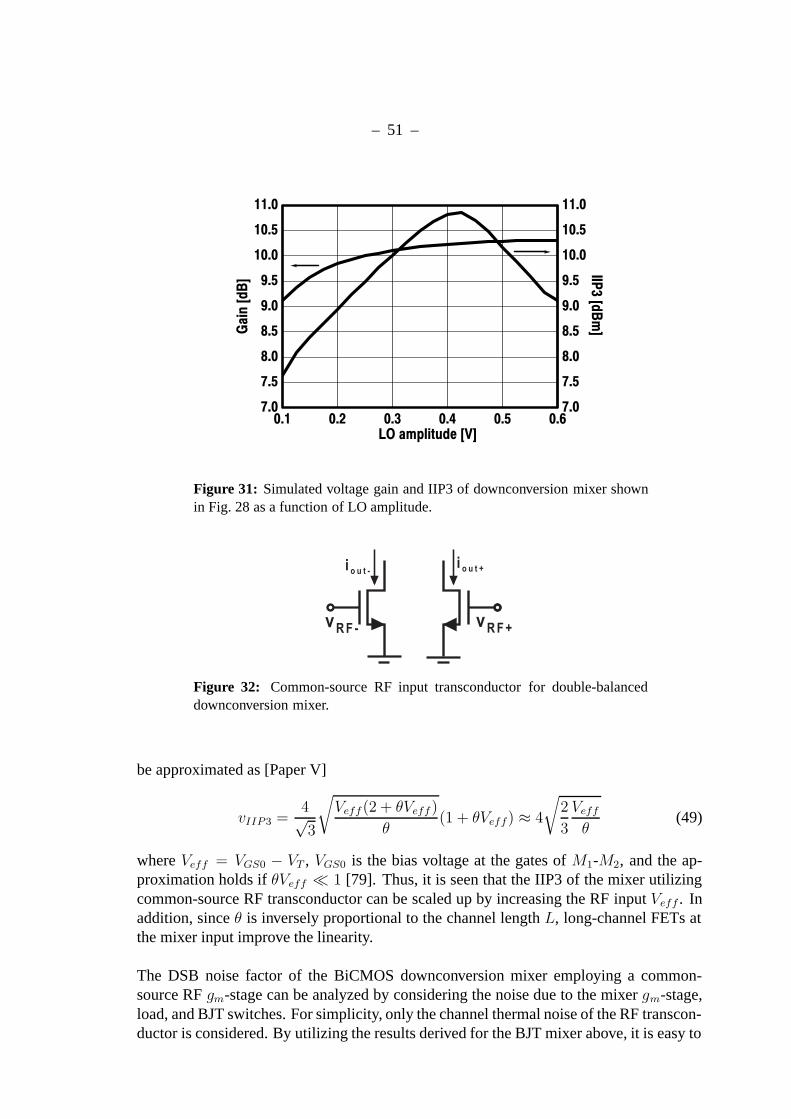
– 51 –
Figure 31: Simulated voltage gain and IIP3 of downconversion mixer shownin Fig. 28 as a function of LO amplitude.
% (
$ + (
% 3
$ + 3
Figure 32: Common-source RF input transconductor for double-balanceddownconversion mixer.
be approximated as [Paper V]
vIIP3 =4√3
√Veff (2 + θVeff )
θ(1 + θVeff) ≈ 4
√2
3
Veffθ
(49)
where Veff = VGS0 − VT , VGS0 is the bias voltage at the gates of M1-M2, and the ap-proximation holds if θVeff 1 [79]. Thus, it is seen that the IIP3 of the mixer utilizingcommon-source RF transconductor can be scaled up by increasing the RF input Veff . Inaddition, since θ is inversely proportional to the channel length L, long-channel FETs atthe mixer input improve the linearity.
The DSB noise factor of the BiCMOS downconversion mixer employing a common-source RF gm-stage can be analyzed by considering the noise due to the mixer gm-stage,load, and BJT switches. For simplicity, only the channel thermal noise of the RF transcon-ductor is considered. By utilizing the results derived for the BJT mixer above, it is easy to
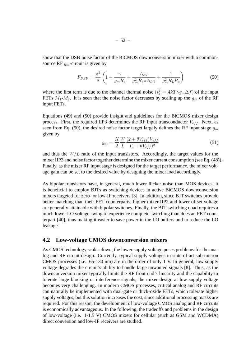
– 52 –
show that the DSB noise factor of the BiCMOS downconversion mixer with a common-source RF gm-circuit is given by
FDSB =π2
8
(1 +
γ
gmRs+
ISWg2mRsπALO
+1
g2mRLRs
)(50)
where the first term is due to the channel thermal noise (i2d = 4kTγgm∆f) of the inputFETs M1-M2. It is seen that the noise factor decreases by scaling up the gm of the RFinput FETs.
Equations (49) and (50) provide insight and guidelines for the BiCMOS mixer designprocess. First, the required IIP3 determines the RF input transconductor Veff . Next, asseen from Eq. (50), the desired noise factor target largely defines the RF input stage gmgiven by
gm =K
2
W
L
(2 + θVeff )Veff(1 + θVeff)2
(51)
and thus the W/L ratio of the input transistors. Accordingly, the target values for themixer IIP3 and noise factor together determine the mixer current consumption (see Eq. (48)).Finally, as the mixer RF input stage is designed for the target performance, the mixer volt-age gain can be set to the desired value by designing the mixer load accordingly.
As bipolar transistors have, in general, much lower flicker noise than MOS devices, itis beneficial to employ BJTs as switching devices in active BiCMOS downconversionmixers targeted for zero- or low-IF receivers [3]. In addition, since BJT switches providebetter matching than their FET counterparts, higher mixer IIP2 and lower offset voltageare generally attainable with bipolar switches. Finally, the BJT switching quad requires amuch lower LO voltage swing to experience complete switching than does an FET coun-terpart [40], thus making it easier to save power in the LO buffers and to reduce the LOleakage.
4.2 Low-voltage CMOS downconversion mixers
As CMOS technology scales down, the lower supply voltage poses problems for the ana-log and RF circuit design. Currently, typical supply voltages in state-of-art sub-micronCMOS processes (i.e. 65-130 nm) are in the order of only 1 V. In general, low supplyvoltage degrades the circuit’s ability to handle large unwanted signals [8]. Thus, as thedownconversion mixer typically limits the RF front-end’s linearity and the capability totolerate large blocking or interference signals, the mixer design at low supply voltagebecomes very challenging. In modern CMOS processes, critical analog and RF circuitscan naturally be implemented with dual-gate or thick-oxide FETs, which tolerate highersupply voltages, but this solution increases the cost, since additional processing masks arerequired. For this reason, the development of low-voltage CMOS analog and RF circuitsis economically advantageous. In the following, the tradeoffs and problems in the designof low-voltage (i.e. 1-1.5 V) CMOS mixers for cellular (such as GSM and WCDMA)direct conversion and low-IF receivers are studied.
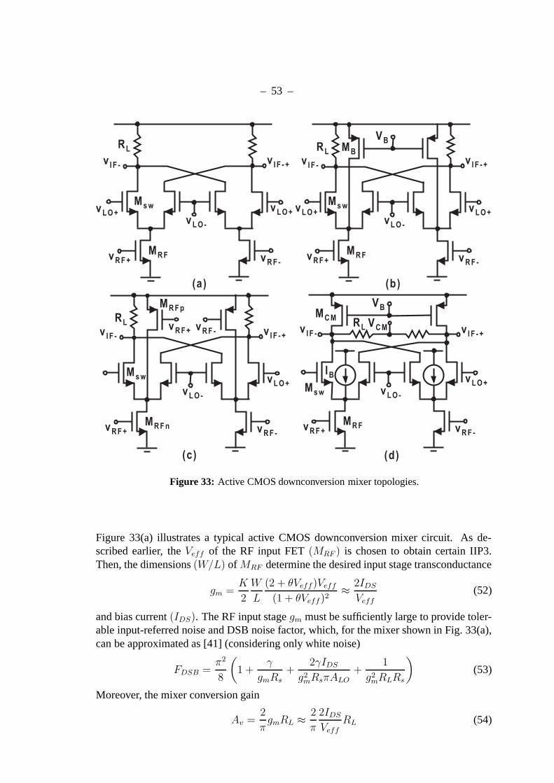
– 53 –
% ( % 3
% (% 3
% (
% 3 % 3 (
- )
% ( % 3
% (% 3
% (
% 3 % 3 (
- )
"
! "
% ( % 3
% (% 3
% 3 % 3 (
- )
% ( % 3
% ( % 3
% (% 3
% 3 % 3 (
- )
! "
!
"
4 7
&
Figure 33: Active CMOS downconversion mixer topologies.
Figure 33(a) illustrates a typical active CMOS downconversion mixer circuit. As de-scribed earlier, the Veff of the RF input FET (MRF ) is chosen to obtain certain IIP3.Then, the dimensions (W/L) of MRF determine the desired input stage transconductance
gm =K
2
W
L
(2 + θVeff)Veff(1 + θVeff)2
≈ 2IDSVeff
(52)
and bias current (IDS). The RF input stage gm must be sufficiently large to provide toler-able input-referred noise and DSB noise factor, which, for the mixer shown in Fig. 33(a),can be approximated as [41] (considering only white noise)
FDSB =π2
8
(1 +
γ
gmRs+
2γIDSg2mRsπALO
+1
g2mRLRs
)(53)
Moreover, the mixer conversion gain
Av =2
πgmRL ≈ 2
π
2IDSVeff
RL (54)
– 54 –
must be high enough to overcome the noise due to the mixer load (RL) and the follow-ing baseband circuits. Unfortunately, as the output common-mode level of the mixer (seeFig. 33(a)) is given by VOCM = VDD−RLIDS, the dc voltage drop (RLIDS) across the re-sistor loads links the maximum obtainable gain to the supply voltage (VDD). Accordingly,at low supply voltage, it is difficult to scale up the gain by increasing RL or IDS withoutVOCM becoming too low for the switch and RF input FETs to remain in saturation. Forthis reason, the realization of a reasonable amount of gain (i.e. 5-15 dB) with sufficientlinearity and tolerable noise performance with the basic mixer shown in Fig. 33(a) at lowvoltage is difficult, at least for cellular applications.
In active current commutating CMOS mixers, flicker noise in the FET switches appears atthe output at baseband without frequency translation [41]. This can significantly raise thenoise factor in a zero- or low-IF receiver particularly in narrow-band applications such asGSM. In a zero- or low-IF receiver, the RF input FETs contribute only white noise at themixer output [83]. Moreover, the mixer load resistors are free of 1/f noise.
In an active mixer, switches contribute flicker noise to the mixer output in two differentways. In direct mechanism, flicker noise modulates the time instants of mixer switchingwhereas in indirect mechanism, it induces current in the tail capacitance, which is com-mutated to the output. At the output of the double-balanced mixer shown in Fig. 33(a),the flicker noise current due to the direct mechanism is given by [41]
io,n = 4ISW × vnS × T
(55)
where ISW is the bias current of each switch pair, vn represents the equivalent flickernoise of the switching quad, S is the slope of the LO signal at the switching instant, andT is the LO period. Thus, the flicker noise due to the direct mechanism can be loweredby reducing ISW , increasing the slope of the LO signal, or by reducing the flicker noisecomponent of the switching FETs (i.e. vn) by increasing the size W × L of the switches.On the other hand, the flicker noise due to the indirect mechanism at the mixer output canbe reduced by reducing the tail capacitance at the common-source of the switches.
In Fig. 33(b), current boosting by a current source (MB) [70] is employed to relax lowvoltage operation, to decouple the conversion gain from the supply voltage, and to reducethe bias current of the switches ISW to lower the flicker noise at the output. Since MBsupplies part of the RF input stage bias current IDS , the larger input stage gm or RL can beutilized with MRF and MSW operating safely in saturation. However, the white noise ofthe current source adds to that of the transconductance stage, increasing the mixer whitenoise factor. In particular, by utilizing the results derived in Section 4.1 and [41], [81],it can be shown that the white-noise DSB noise factor of the mixer employing currentboosting can be approximated as
FDSB =π2
8
(1 +
γngmRs
+γpgmBg2mRs
+2γnISW
g2mRsπALO
+1
g2mRLRs
)(56)
where the third term is due to the channel thermal noise of MB (i2d = 4kTγpgmB∆f), andγn and γp are the channel current noise factors of NMOS and PMOS transistors, respec-
– 55 –
tively. For a given bias current, PMOS sources MB should be biased at large Veff,B ortheir (W/L)B should be small to lower their thermal noise at the mixer output.
The current boosting technique can also be modified to include RF signal amplification inthe bias transistor MB , as shown in Fig. 33(c) [82]. As the total RF input stage transcon-ductance of the mixer with a complementary RF input stage is (gmn + gmp) where gmnand gmp are the transconductances of MRFn and MRFp, respectively, lower RL can beutilized at the mixer output to realize a given voltage gain. This enhances the operation atlow voltage. In addition, since for given current consumption and voltage gain the mixerwith the complementary input stage has higher total transconductance than the mixer withconventional current boosting, the mixer with complementary RF input stage has lowerinput-referred noise. As a matter of fact, it can be shown that the white-noise DSB noisefactor of the mixer shown in Fig. 33(c) can be estimated as
FDSB=π2
8
(1+
γngmn+γpgmp(gmn+gmp)2Rs
+2γnISW
(gmn+gmp)2RsπALO+
1
(gmn+gmp)2RsRL
)(57)
At low supply voltage, the nonlinearity contribution of the mixer switching quad MSW isnot usually negligible. The FETs in the commutating differential pair create nonlinearitydue to the signal-dependent current division [51]. Sharp transitions in the LO waveformlower the distortion and flicker noise due to the mixer switches [31] and thus it is oftenbeneficial to raise the amplitude of the LO signal to sharpen the transition. Unfortunately,at low supply voltage, only a small headroom margin for the mixer switches to remain insaturation can be guaranteed and high LO amplitude reduces this margin further. Thus, atoo-large LO amplitude will force the switch FETs into the triode region and degrade themixer linearity due to the nonlinear mixer output resistance. Mixers employing the cur-rent boosting technique and complementary RF input stage reduce the bias current ISWof the mixer switches in order to enable low-voltage operation and to lower the flickernoise at the output. Unfortunately, reducing the bias current of the switches raises theimpedances seen at their sources, increases the RF voltage swing at the common-sourcenode of the switches, and therefore degrades the mixer linearity and bandwidth [83].Thus, for given switch FET dimensions, mixer switches must be biased at sufficient cur-rent to guarantee that the mixer switching quad do not limit the mixer third-order linearity.Unfortunately, for given voltage gain, increasing the bias current of the switches lowersthe output common-mode level of the mixers shown in Figures 33(a)-(c) and reduces thesaturation margin of the transistors. For these reasons, at low supply voltage the mix-ers shown in Figures 33(a)-(c) are usually too nonlinear for cellular applications, at leastwhen a practical amount of conversion voltage gain (i.e. 5-15 dB) is to be implemented.For instance, simulated in the 0.13-µm CMOS technology, the mixer with a complemen-tary RF input stage shown in Fig. 33(c) achieves a voltage conversion gain of 10 dB, IIP3of +1 dBm, and a white-noise DSB-NF (10 log(FDSB)) of 4 dB with respect to the noisein a 100-Ω differential resistor. Its 1/f corner frequency lies at 470 kHz. Unfortunately,an IIP3 in the order of +1 dBm is not usually sufficient for cellular systems. Moreover, al-though the mixer has a very low white-noise NF, the flicker noise increases the integratedNF significantly. For instance, assuming the DSB-NF in GSM and WCDMA direct con-version receiver is integrated over a bandwidth of 100 Hz-135 kHz and 10 kHz-1.92 MHz,
– 56 –
the integrated DSB-NF for GSM and WCDMA applications is about 18 dB and 7.5 dB,respectively. The mixer draws 4 mA from a 1.2-V supply.
By utilizing a common-mode feedback (CMFB) circuit at the mixer output (Fig. 33(d)),the bias current of the mixer switches can be increased to improve the mixer linearitywithout lowering the common-mode level at the output [30]. In addition, the conversiongain can be increased by scaling up the differential load resistors without altering theoutput dc level. Unfortunately, noise from the two CMFB current source FETs (MCM )appears as differential noise at the mixer output. In this case, the white-noise DSB noisefactor of the mixer can be approximated as
FDSB =π2
8
(1 +
γngmRs
+γpgmBg2mRs
+2γnISW
g2mRsπALO
+1
g2mRLRs
+γpgmCMg2mRs
)(58)
where the last term is due to the channel thermal noise of MCM (i2d = 4kTγpgmCM∆f).To fit into a low supply voltage, CMFB FETs should be biased at small Veff,CM , whichunfortunately increases their gmCM = (2IDS,CM)/Veff,CM and enhances their noise. Inaddition, the flicker noise of the CMFB FETs further increases the mixer noise factor,particularly in narrow-band applications. To reduce the flicker noise due to the CMFBFETs, large-area devices have to be applied. Moreover, although increasing the bias cur-rent of the mixer switches improves the mixer linearity, it increases the flicker noise dueto the switches at the output (see Eq. (55)). For instance, simulated in the 0.13-µmCMOStechnology, the mixer shown in Fig. 33(d) achieves a gain of 10 dB, IIP3 of +6 dBm, anda white-noise DSB-NF of 9 dB. Its 1/f corner frequency is as high as 1.1 MHz. As aresult, its integrated DSB-NF for GSM and WCDMA zero-IF receiver is as high as 27 dBand 16 dB, respectively. The mixer draws 4 mA from a 1.2-V supply. As a conclusion,although the mixer with active loads shown in Fig. 33(d) has higher linearity, it is usuallytoo noisy at least for narrow-band zero- or low-IF receivers.
An input-referred flicker noise in FET can be approximated as [37]
v2n =
KfWLCoxf
∆f (59)
where Kf is the flicker noise coefficient and Cox is the oxide capacitance. Due to theburied channel conduction induced by the threshold adjust implant [41], the flicker noisecoefficient of PMOS devices is lower than the corresponding coefficient of NMOS transis-tors. For this reason, it can be advantageous to employ PMOS instead of NMOS switchesin an active CMOS downconversion mixer, in order to lower the flicker noise at the mixeroutput [84], [85]. In Fig. 34(a), a current-folding downconversion mixer utilizing PMOSswitches is illustrated [4]. Besides utilizing the PMOS switching quad, the flicker noise atthe mixer output can be lowered by scaling up the PMOS switch gate area W ×L and bysharpening the transitions in the LO signal waveform by raising the LO amplitude. Thiscan be accomplish, for instance, by utilizing CMOS inverters as LO buffers, which canprovide almost rail-to-rail LO swing. In addition, as the RF input and switching FETsin the current-folding mixer can be biased at different currents, the bias current of the

– 57 –
% ( % 3
% 3
% (
% 3% 3 (
- ) % (
! "
"
% (
% 3
% (
% 3% 3 (
- ) % (
% 3
Figure 34: Folded CMOS downconversion mixer circuits.
switches can be reduced to lower the flicker noise at the output without altering the RFinput bias. For the same reason, the mixer gain can be independently increased either byincreasing the RF input stage gm or RL. However, as in a mixer with current boosting (seeFig. 33(b)), the white noise of the current source MB adds to that of the RF input stage,increasing the mixer white noise factor significantly [4]. In particular, the white-noiseDSB noise factor of the current-folded mixer shown in Fig. 34(a) can be approximated as
FDSB =π2
8
(1 +
γngmRs
+γpgmBg2mRs
+2γpISW
g2mRsπALO
+1
g2mRLRs
)(60)
where the third term is due to the channel thermal noise of MB (i2d = 4kTγpgmB∆f) .
In order to operate properly at low supply voltage, PMOS current sources MB shownin Fig. 34(a) must be biased at small or moderate Veff,B, which unfortunately increasestheir thermal noise contribution at the mixer output (i2d = 4kTγp∆f(2IB/Veff,B)). Inpractice, the limited Veff,B of MB results in a several-dB increase in the mixer whitenoise figure. In addition, the current sources introduce additional parasitic capacitance
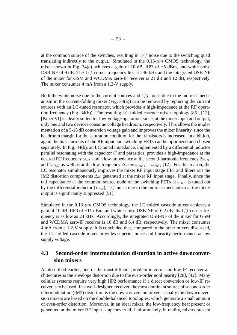
– 58 –
at the common source of the switches, resulting in 1/f noise due to the switching quadtranslating indirectly to the output. Simulated in the 0.13-µm CMOS technology, themixer shown in Fig. 34(a) achieves a gain of 10 dB, IIP3 of +5 dBm, and white-noiseDSB-NF of 9 dB. The 1/f corner frequency lies at 246 kHz and the integrated DSB-NFof the mixer for GSM and WCDMA zero-IF receiver is 21 dB and 12 dB, respectively.The mixer consumes 4 mA from a 1.2-V supply.
Both the white noise due to the current sources and 1/f noise due to the indirect mech-anism in the current-folding mixer (Fig. 34(a)) can be removed by replacing the currentsources with an LC-tuned resonator, which provides a high-impedance at the RF opera-tion frequency (Fig. 34(b)). The resulting LC-folded cascode mixer topology [86], [12],[Paper VI] is ideally suited for low-voltage operation, since, at the mixer input and output,only one and two devices consume voltage headroom, respectively. This allows the imple-mentation of a 5-15 dB conversion voltage gain and improves the mixer linearity, since theheadroom margin for the saturation condition for the transistors is increased. In addition,again the bias currents of the RF input and switching FETs can be optimized and chosenseparately. In Fig. 34(b), an LC-tuned impedance, implemented by a differential inductorparallel resonating with the capacitor C and parasitics, provides a high-impedance at thedesired RF frequency ωRF and a low-impedance at the second-harmonic frequency 2ωRFand 2ωLO as well as at the low-frequency ∆ω = ωRF1 − ωRF2 [12]. For this reason, theLC resonator simultaneously improves the mixer RF input stage IIP3 and filters out theIM2 distortion components ∆ω generated at the mixer RF input stage. Finally, since thetail capacitance at the common-source node of the switching FETs at ωRF is tuned outby the differential inductor (Lmd), 1/f noise due to the indirect mechanism at the mixeroutput is significantly suppressed [51].
Simulated in the 0.13-µm CMOS technology, the LC-folded cascode mixer achieves again of 10 dB, IIP3 of +11 dBm, and white-noise DSB-NF of 6.2 dB. Its 1/f corner fre-quency is as low as 24 kHz. Accordingly, the integrated DSB-NF of the mixer for GSMand WCDMA zero-IF receiver is 10 dB and 6.4 dB, respectively. The mixer consumes4 mA from a 1.2-V supply. It is concluded that, compared to the other mixers discussed,the LC-folded cascode mixer provides superior noise and linearity performance at lowsupply voltage.
4.3 Second-order intermodulation distortion in active downconver-sion mixers
As described earlier, one of the most difficult problem in zero- and low-IF receiver ar-chitectures is the envelope distortion due to the even-order nonlinearity [28], [42]. Manycellular systems require very high IIP2 performance if a direct conversion or low-IF re-ceiver is to be used. In a well-designed receiver, the most dominant source of second-orderintermodulation (IM2) distortion is the downconversion mixer. Usually the downconver-sion mixers are based on the double-balanced topologies, which generate a small amountof even-order distortion. Moreover, in an ideal mixer, the low-frequency beat present orgenerated at the mixer RF input is upconverted. Unfortunately, in reality, mixers present

– 59 –
a finite feedthrough from the RF input to the IF output, which results in a finite IIP2 [40].
As discussed in Section 4.1, most of the active double-balanced mixers utilized in wire-less receivers are realized as Gilbert-type mixers [78]. In general, both the RF inputtransconductor and switching devices contribute to the mixer nonlinearity, and the mixerIIP2 is determined by the mixer second-order nonlinearity, mismatches, and offsets. Asa conclusion, in order to maximize the mixer IIP2, it is essential to develop techniquesfor minimizing the IM2 products generated in the mixer, since the device matching andoffsets cannot be improved beyond certain limits. On the other hand, in order to minimizethe IM2 distortion due to the self-mixing, the RF-to-LO coupling has to be minimizedand a sufficiently large LO amplitude has to applied [28].
4.3.1 IM2 distortion suppression techniques in mixer RF input transconductors
In a perfectly balanced mixer, stimulated and sensed differentially, the IM2 componentsat the mixer output are presented as common-mode signals with equal amplitude and aretherefore cancelled. Unfortunately, in the presence of offsets and mismatches, the cancel-lation is not perfect, which results in finite mixer IIP2. If the second-order nonlinearityof the mixer switching devices is neglected, the IIP2 of a double-balanced mixer can beapproximated as [42]
vIIP2 =
√2 · vIIP2,gm
πηnom· 4
(2∆η(∆gm + ∆ARF ) + ∆R(1 + ∆gm)(1 + ∆ARF ))(61)
where ηnom is the nominal value of the duty cycle in a single-switch, ∆η is the mismatchin the duty cycles, ∆gm is the mismatch between the mixer RF input transconductances,∆ARF is the amplitude imbalance of the RF signal, ∆R is the imbalance of the mixerload resistances, and vIIP2,gm is the single-ended (or common-mode) IIP2 of the mixerRF input transconductor, measured from the single-ended output of the transconductor.
From Eq. (61), it is seen that due to the mismatch, for instance, in mixer load resistors andswitching transistors, the IM2 currents generated by the RF input transconductor are di-rectly transmitted or leaked to the mixer output. The corresponding direct leakage mech-anism can be lowered by employing large-area switching transistors for better matchingand by utilizing a large LO amplitude [28], [52]. On the other hand, the IM2 productsgenerated by the RF input transconductor can also be transferred to the mixer output viaan indirect mechanism that is induced by the parasitic capacitance at the common-emitter(or source) node of the switching stage [28] (see Fig. 35). Fortunately, both of thesemechanisms can be, at least ideally, eliminated by minimizing the level of the common-mode IM2 components in the output current of the RF transconductor. Simultaneously,the matching requirement for the mixer output resistances can be lowered and the needfor mixer IIP2 calibration [6] or trimming [42] can be reduced or even avoided.
The common-mode IM2 products generated in the mixer RF input transconductor canbe eliminated, or at least, in practice, minimized in the presence of offsets [88], [89], by afully differential RF input stage such as a differential pair [28]. Unfortunately, as the IIP3

– 60 –
9 : ; <
% (
% 3
% (
& *
Figure 35: Parasitic capacitance Cpar loading common-emitter node ofswitching pair.
% (
$ + 3
% 3
$ + (
7 , 7 ,
! "
$ + (
% 3
$ + 3
" % (
. 0
Figure 36: Circuit techniques to minimize the level of common-mode IM2products generated at mixer RF input stage.
of the differential pair is worse than the IIP3 of the common-source (emitter) transconduc-tor at a given bias [90] (see, for instance, Equations (37) and (38)), the common-source(emitter) RF input transconductor is usually preferred to the differential pair. Moreover,as supply voltage scales down with transistor technology, the realization of a Gilbert-typemixer with a differential pair RF input stage becomes difficult.
An RF input transconductor featuring a large degeneration resistance at low frequenciesand a low degeneration impedance at RF operation frequency can simultaneously obtaina high IIP3 and a low level of IM2 components at its output current [92]. However, atlow supply voltage, a large resistor cannot usually be used due to the voltage headroomlimitations. Instead, as shown in Fig. 36(a), an FET biased in the triode region (Mdeg) inparallel with a degeneration capacitance (Cdeg) can realize the desired function. Never-theless, Mdeg still consumes some voltage headroom and its nonlinear output resistancemay cause additional distortion.
– 61 –
The common-mode IM2 products generated in the mixer RF input transconductor canalso be eliminated by ac-coupling the RF input stage from the switches [21], as illus-trated in Fig. 36(b). Unfortunately, additional current sources (IB) and load resistors (R)needed in the RF input stage increase the mixer noise factor and introduce additional para-sitic capacitance at the common-node of the switching devices. This parasitic capacitanceincreases the second-order nonlinearity of the switching devices [28] and translates 1/fnoise due to the switching quad indirectly to the mixer output [41].
For the reason that the common-source transconductor biased at a certain Veff exhibitshigher IIP3 than the differential pair at equal bias [90], most of the reported low-voltageCMOS downconversion mixers usually utilize the common-source transconductor as theirRF input stage (see Fig. 37(a)) [2], [3], [4], [5], [90]. Unfortunately, the drawback of thecommon-source circuit is its second-order intermodulation characteristics. Namely, it iseasy to show that if the common-source circuit is excited with two closely spaced RF sig-nals with an equal amplitude vRF (t) = vin cos(ω1t) + vin cos(ω2t), the common-sourcecircuit displays a common-mode IM2 component at the frequency of f1 − f2 at its output[Paper V]. In a perfectly balanced mixer, this common-mode component is cancelled inthe mixer’s differential output. However, in the presence of mismatches, the cancellationis not perfect. In particular, it can be shown that the IIP2 of the common-source RF inputtransconductor, measured at the single-ended transconductor output (i.e. iout+ or iout− inFig. 37(a)), can be approximated as [79], [Paper V]
vIIP2 = 2Veff(1 + θVeff )(2 + θVeff ) ≈ 4Veff (62)
which represents the differential RF input voltage. Both input FETs (M1 and M2) experi-ence half of this voltage. Accordingly, in the sense of the entire mixer IIP2, the presenceof the common-mode IM2 component at the output current is a clear drawback of thecommon-source RF transconductor.
Figure 37(b) illustrates a simple biasing circuit technique, which can be employed tocancel the IM2 distortion in the common-source transconductor [91], [Paper V]. In thiscircuit, the original bias transistor shown in Fig. 37(a) is divided into two equal-sizedFETs half the size W/(2L) of the original transistor. Moreover, the differential RF inputsignal is also applied to the gates of the bias FETs (MB1-MB2). Assuming that both thetransconductors shown in Figures 37(a) and (b) employ equal sized FETs and bias cur-rents, both transconductors provide an equal input stage gm.
The operation principle of the IM2 cancellation technique shown in Fig. 37(b) can beunderstood by considering the IM2 product at the output current of the nonlinear transcon-ductance, such as a single FET or BJT, which in general is given as [94]
iout+,∆ω = iNL2 + gmvc,∆ω = K2gmv2c,ω1
+ gmvc,∆ω =1
2
∂gm∂vc
v2c,ω1
+ gmvc,∆ω (63)
where gm is the transconductance, vc is the voltage (i.e. vGS of FET) that controls thenonlinear transconductance, and K2gm
is the second-order nonlinearity coefficient of the

– 62 –
% (
$ + 3
% 3
$ + (
" "
"
% 3 % (
" "
" " 0
0 0
$ + 3 $ + (
0
Figure 37: (a) Traditional common-source RF transconductor. (b) Biasingtechnique for cancellation of common-mode IM2 distortion in common-sourcecircuit.
nonlinear transconductance. It is seen that iout+,∆ω consists of two different components.The first component is due to K2gm
of the transconductor. This term also depends on thevalue of the control voltage vc,ω1 at the fundamental frequency ω1. On the other hand,the value of the control voltage vc,∆ω at ∆ω also has effect on iout+,∆ω via gm, as seenfrom Eq. (63). Now, if by some means the value of vc,∆ω = −iNL2/gm at ∆ω can begenerated, the IM2 component at the transconductor output can be cancelled. As a matterof fact, by applying a direct calculation of nonlinear responses [94], [Paper V], it can beshown that the bias circuit shown in Fig. 37(b) at ∆ω generates the required control volt-age vc,∆ω = −iNL2/gm , which cancels the common-mode IM2 component at the outputof the common-source transconductor. The fact that the RF input transconductor shownin Fig. 37(b) does not display any common-mode IM2 components at its output is a clearimprovement to the conventional common-source RF transconductor with respect to theIIP2 of the entire mixer.
The proposed IIP2 enhancement circuit has properties similar to the conventional dif-ferential pair in the sense that it ideally displays no IM2 distortion, provided that thetransconductor is excited differentially and all the transistors in the circuit match witheach other. However, as in the conventional differential pair, in the presence of offsets

– 63 –
and mismatches, a small residual IM2 distortion is generated [Paper V]. Nevertheless,on the contrary to the differential pair, the proposed transconductor circuit is very suit-able for operation at low supply voltage, because it has only one device stacked betweenthe transconductor input and output. In the conventional differential pair, two devicesconsume the voltage headroom. It is also easy to show that, for given bias and devicedimensions (and thus for given RF input gm), the proposed RF input transconductor hasa noise performance equivalent to the traditional common-source transconductor [PaperV]. Finally, for given Veff , the IIP3 of the proposed transconductor is slightly higher thanthe IIP3 of the differential pair transconductor. In particular, the IIP3 of the RF input stageshown in Fig. 37(b) can be approximated as [Paper V]
vIIP3 =4Veff(1 + θVeff )(2 + θVeff )√
4 + 3θVeff(2 + θVeff )≈ 4Veff (64)
where the approximation holds for long-channel FETs (i.e. when θVeff 1).
From Eq. (64) it is seen that similarly as the IIP3 of the conventional common-sourceRF input transconductor (Fig. 37(a)), the IIP3 of the proposed transconductor (Fig. 37(b))can be scaled up by biasing the input FET at larger Veff .
Fig. 38 plots the simulated IIP3 of the proposed common-source transconductor (0.35-µm NMOSFET in 0.35-µm BiCMOS) versus the effective gate voltage, together withtheoretical values (θ = 1.5 V −1). The theoretical values are calculated from Eq. (64), asthe corresponding power in dBm dissipated in a 100-Ω differential resistor. In addition,here the comparison between theory and simulation is made only for Veff ≥ 300 mV,because Eq. (48), used to derive Eq. (64), is a reasonable estimate for the drain currentonly in the strong inversion. For weak and moderate inversion, appropriate model forthe drain current has to be applied [95]. Nevertheless, from Fig. 38 it is concluded thatfor Veff ≥ 300 mV in strong inversion, simulated values compare well with theoreticalvalues.
The IIP3 of the proposed transconductor is larger than the IIP3 of the differential pair by afactor of
√3(2 + θVeff(2 + θVeff ))/(4 + 3θVeff(2 + θVeff )) when biased at equal Veff
[Paper V]. At small Veff (θVeff 1), the difference is about√
3/2 i.e. 1.8 dB. However,at large Veff (θVeff 1), the transconductors have approximately equal IIP3s. On theother hand, compared to the conventional common-source transconductor, the proposedRF transconductor has, by a factor of
√(4 + 3θVeff(2 + θVeff ))/(3θVeff(2 + θVeff )) ≈√
2/(3θVeff) smaller IIP3 at a given bias, assuming θVeff 1. Notice that as Veff isincreased, the difference between the IIP3s of the conventional and proposed transcon-ductors is decreased.
Figure 39(a) illustrates a conventional resistively degenerated common-emitter mixer RFinput transconductance circuit. Suppose that the current mirror ratio is A as shown. Thebias BJT (QBb) provides base currents for the main bias BJT (Qb) and RF BJTs (Q1-Q2). As in the conventional common-source circuit, the output current of the degeneratedcommon-emitter RF transconductor displays a common-mode IM2 component, which is a
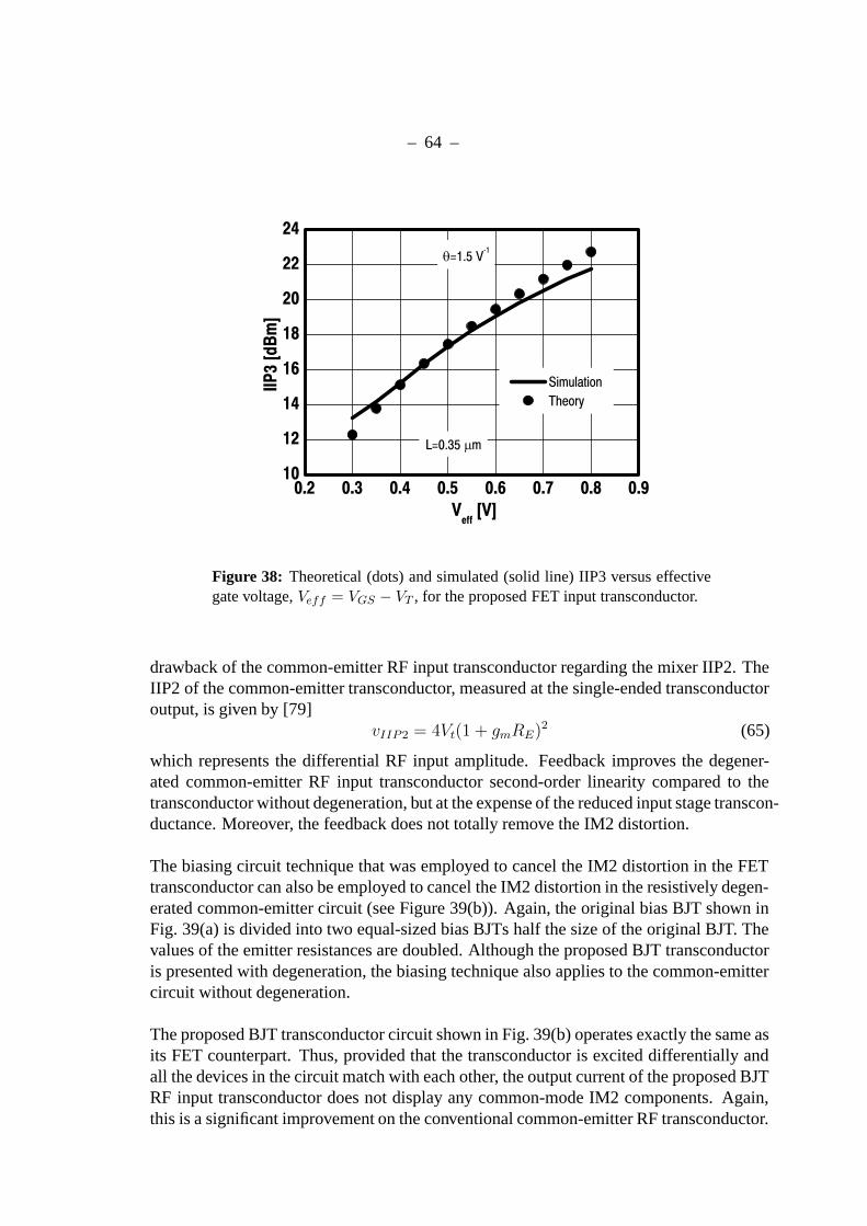
– 64 –
Figure 38: Theoretical (dots) and simulated (solid line) IIP3 versus effectivegate voltage, Veff = VGS − VT , for the proposed FET input transconductor.
drawback of the common-emitter RF input transconductor regarding the mixer IIP2. TheIIP2 of the common-emitter transconductor, measured at the single-ended transconductoroutput, is given by [79]
vIIP2 = 4Vt(1 + gmRE)2 (65)
which represents the differential RF input amplitude. Feedback improves the degener-ated common-emitter RF input transconductor second-order linearity compared to thetransconductor without degeneration, but at the expense of the reduced input stage transcon-ductance. Moreover, the feedback does not totally remove the IM2 distortion.
The biasing circuit technique that was employed to cancel the IM2 distortion in the FETtransconductor can also be employed to cancel the IM2 distortion in the resistively degen-erated common-emitter circuit (see Figure 39(b)). Again, the original bias BJT shown inFig. 39(a) is divided into two equal-sized bias BJTs half the size of the original BJT. Thevalues of the emitter resistances are doubled. Although the proposed BJT transconductoris presented with degeneration, the biasing technique also applies to the common-emittercircuit without degeneration.
The proposed BJT transconductor circuit shown in Fig. 39(b) operates exactly the same asits FET counterpart. Thus, provided that the transconductor is excited differentially andall the devices in the circuit match with each other, the output current of the proposed BJTRF input transconductor does not display any common-mode IM2 components. Again,this is a significant improvement on the conventional common-emitter RF transconductor.

– 65 –
% ( % 3
$ + (
"
"
% (
"
"
$ + 3
5 ;
"
"
$ + (
$ + 3
" "
"
% 3
Figure 39: (a) Traditional resistively degenerated common-emitter RFtransconductor. (b) Biasing technique for cancellation of common-mode IM2distortion in common-emitter circuit.
The IIP3 of the proposed BJT transconductor shown in Fig. 39(b) can be estimated as[Paper V]
vIIP3 = 4√
2Vt(1 + gmRE)2
√1 + 2gmRE
(66)
As the IIP3 of the conventional degenerated common-emitter RF input transconductorshown in Fig. 39(a), the IIP3 of the proposed transconductor (Fig. 39(b)) can be improvedby increasing the loop gain of the negative feedback, i.e. scaling up IC or RE.
Fig. 40 plots the simulated IIP3 of the proposed BJT input transconductor, realized in0.35-µm BiCMOS, versus the collector biasing current, together with theoretical values(RE = 40 Ω). The latter are calculated from Eq. (66), as the corresponding power in
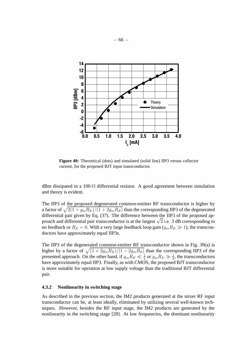
– 66 –
Figure 40: Theoretical (dots) and simulated (solid line) IIP3 versus collectorcurrent, for the proposed BJT input transconductor.
dBm dissipated in a 100-Ω differential resistor. A good agreement between simulationand theory is evident.
The IIP3 of the proposed degenerated common-emitter RF transconductor is higher bya factor of
√2(1 + gmRE)/(1 + 2gmRE) than the corresponding IIP3 of the degenerated
differential pair given by Eq. (37). The difference between the IIP3 of the proposed ap-proach and differential pair transconductor is at the largest
√2 i.e. 3 dB corresponding to
no feedback or RE = 0. With a very large feedback loop gain (gmRE 1), the transcon-ductors have approximately equal IIP3s.
The IIP3 of the degenerated common-emitter RF transconductor shown in Fig. 39(a) ishigher by a factor of
√(1 + 2gmRE)/|1 − 2gmRE| than the corresponding IIP3 of the
presented approach. On the other hand, if gmRE 12
or gmRE 12, the transconductors
have approximately equal IIP3. Finally, as with CMOS, the proposed BJT transconductoris more suitable for operation at low supply voltage than the traditional BJT differentialpair.
4.3.2 Nonlinearity in switching stage
As described in the previous section, the IM2 products generated at the mixer RF inputtransconductor can be, at least ideally, eliminated by utilizing several well-known tech-niques. However, besides the RF input stage, the IM2 products are generated by thenonlinearity in the switching stage [28]. At low frequencies, the dominant nonlinearity
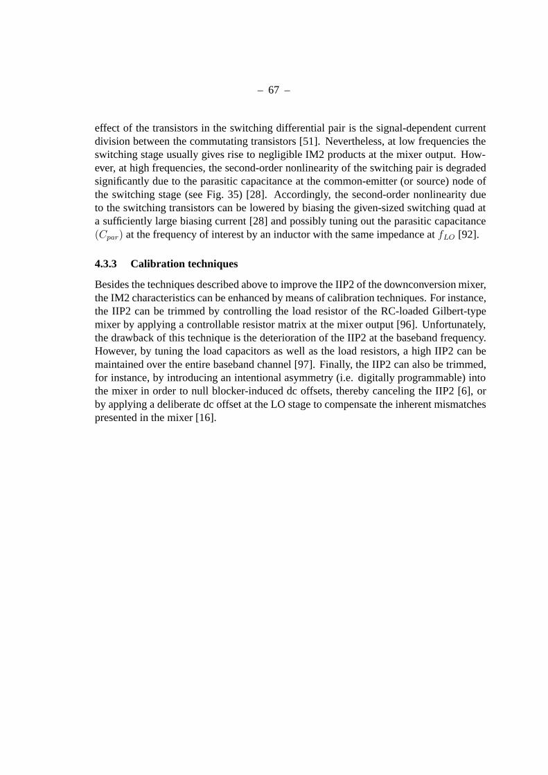
– 67 –
effect of the transistors in the switching differential pair is the signal-dependent currentdivision between the commutating transistors [51]. Nevertheless, at low frequencies theswitching stage usually gives rise to negligible IM2 products at the mixer output. How-ever, at high frequencies, the second-order nonlinearity of the switching pair is degradedsignificantly due to the parasitic capacitance at the common-emitter (or source) node ofthe switching stage (see Fig. 35) [28]. Accordingly, the second-order nonlinearity dueto the switching transistors can be lowered by biasing the given-sized switching quad ata sufficiently large biasing current [28] and possibly tuning out the parasitic capacitance(Cpar) at the frequency of interest by an inductor with the same impedance at fLO [92].
4.3.3 Calibration techniques
Besides the techniques described above to improve the IIP2 of the downconversion mixer,the IM2 characteristics can be enhanced by means of calibration techniques. For instance,the IIP2 can be trimmed by controlling the load resistor of the RC-loaded Gilbert-typemixer by applying a controllable resistor matrix at the mixer output [96]. Unfortunately,the drawback of this technique is the deterioration of the IIP2 at the baseband frequency.However, by tuning the load capacitors as well as the load resistors, a high IIP2 can bemaintained over the entire baseband channel [97]. Finally, the IIP2 can also be trimmed,for instance, by introducing an intentional asymmetry (i.e. digitally programmable) intothe mixer in order to null blocker-induced dc offsets, thereby canceling the IIP2 [6], orby applying a deliberate dc offset at the LO stage to compensate the inherent mismatchespresented in the mixer [16].

– 68 –
5 Interface Issues in RF Front-End
In RFIC design, interface issues are very important. Accordingly, since in the RF front-end different blocks have a strong effect on each other, these circuits have to be designedand simulated together. In addition, the interfaces to the circuits preceding and followingthe RF front-end have to be modeled and simulated properly. Only in this way, can anoptimum performance be achieved in practice.
5.1 Preselect filter-LNA
As described earlier, the input impedance of the LNA has to be designed to match thecharacteristic impedance, e.g., 50 Ω, of the external preselect or duplex filter (see Fig. 1).Moreover, as the parallel capacitance Cp due to the package and ESD parasitics drasti-cally lowers the input impedance level of the inductively degenerated common-emitter(source) LNA, an impedance transformation network, in general, is needed to transformthe LNA input impedance upwards. Moreover, if the real part of the impedance lookinginto the base or gate of the LNA input transistor (see for instance Ring in Fig. 13) is verylow compared to the source impedance Rs, an impedance transformation network with alarge scaling factor is required accordingly. Unfortunately, when scaling the impedanceby a large factor, the required Q factor of the matching circuit grows quadratically andthe LNA input matching becomes sensitive to parasitics, process and component varia-tions [36]. This will also result in narrow-band input matching (i.e. in a bandwidth forwhich S11 < −10 dB). Thus, for this reason, it is important to provide sufficiently largereal part of the impedance looking into the base or gate of the LNA input transistor by anappropriate circuit design.
Figure 41 illustrates two possible ways to implement the input impedance matching net-work of the inductively degenerated common-source LNA. It is assumed that, due to thepackage and ESD parasitics, the LNA input impedance needs to be transformed upwards.Moreover, usually the requirement for the LNA noise factor dictates that the matchingcomponents need to be realized as external high-Q elements. In Fig. 41(a), the match-ing network is implemented with series inductors and a parallel capacitor, whereas, inFig. 41(b), a parallel inductor and series capacitors realize the input matching, respec-tively. Since off-chip lumped capacitors are usually cheaper than the corresponding in-ductors, the matching network shown in Fig. 41(b) results in lower cost. Moreover, thematching network shown in Fig. 41(b) automatically ac-couples the LNA input from thepreceding balun or filter. If the ac-coupling is required, the matching network illustratedin Fig. 41(a) needs additional series capacitors for this purpose.
5.2 LNA-downconversion mixer
In zero- and low-IF receivers, LNA typically drives I and Q mixers directly on-chip. How-ever, if for some reason an external bandpass filter must be utilized between the LNA andmixer [16], both the LNA output and mixer input need to be matched to the characteristicimpedance of the filter. Nevertheless, in the case of direct on-chip connection between
– 69 –
3
3
Figure 41: LNA input matching networks.
the LNA and mixer, the LNA-mixer interface usually operates in the voltage domain, i.e.both the LNA output and the mixer input employ voltage-mode signal processing. More-over, in most cases, it is beneficial to utilize ac-coupling at the interface. This way thelow-frequency IM2 distortion generated in the LNA can be filtered out and the dc-levelsat the LNA output and at the mixer input can be set independently.
The input stage of the inductively degenerated common-source LNA provides its out-put signal in current domain. Moreover, since the switching quad of a Gilbert-type mixeralso commutes current, translating it in frequency, these circuits can be cascaded in cur-rent [51]. Eliminating the voltage-to-current conversion at the mixer RF input stage alsoremoves the associated source of nonlinearity. Accordingly, the resulted current-modecascade LNA and mixer, or simply a low-noise mixer, can possibly achieve higher linear-ity than a conventional LNA and mixer cascaded in the voltage domain.
In a zero- or low-IF receiver, the LNA must drive two mixers to produce quadrature out-puts. With the LNA and mixer cascaded in the current domain, this can be realized bycoupling the differential LNA into the tails of two commutating differential pairs in paral-lel, which together comprise two double-balanced mixers [51] (see Fig. 42). The voltageconversion gain of the low-noise mixer shown in Fig. 42 can be approximated as
Av =1
2· 2
π·Gm,LNARL =
Gm,LNARLπ
(67)
where Gm,LNA is the input stage transconductance of the LNA and the factor of (1/2)results from the fact that the LNA drives two mixers in parallel. The voltage gain ofthe conventional RF front-end utilizing the voltage-mode interface between the LNA andmixers is given by
Av = Gm,LNARL,LNA · 2
π·Gm,mixerRL,mixer (68)
where RL,LNA is the LNA load impedance at the RF frequency, Gm,mixer is the mixer RFinput stage transconductance, and RL,mixer is the mixer load resistance. Eq. (68) assumesthat I and Q mixers have their own RF input stage. By comparing Equations (67) and (68),
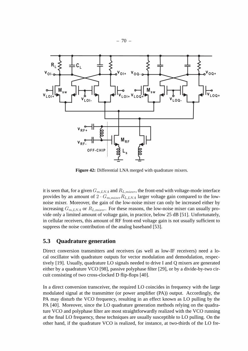
– 70 –
% (
% 3
% (% 3
% (
% 3 % (
- ) % (% 3
% (
% 3% (
- )
3
-
Figure 42: Differential LNA merged with quadrature mixers.
it is seen that, for a givenGm,LNA andRL,mixer, the front-end with voltage-mode interfaceprovides by an amount of 2 · Gm,mixerRL,LNA larger voltage gain compared to the low-noise mixer. Moreover, the gain of the low-noise mixer can only be increased either byincreasing Gm,LNA or RL,mixer. For these reasons, the low-noise mixer can usually pro-vide only a limited amount of voltage gain, in practice, below 25 dB [51]. Unfortunately,in cellular receivers, this amount of RF front-end voltage gain is not usually sufficient tosuppress the noise contribution of the analog baseband [53].
5.3 Quadrature generation
Direct conversion transmitters and receivers (as well as low-IF receivers) need a lo-cal oscillator with quadrature outputs for vector modulation and demodulation, respec-tively [19]. Usually, quadrature LO signals needed to drive I and Q mixers are generatedeither by a quadrature VCO [98], passive polyphase filter [29], or by a divide-by-two cir-cuit consisting of two cross-clocked D flip-flops [40].
In a direct conversion transceiver, the required LO coincides in frequency with the largemodulated signal at the transmitter (or power amplifier (PA)) output. Accordingly, thePA may disturb the VCO frequency, resulting in an effect known as LO pulling by thePA [40]. Moreover, since the LO quadrature generation methods relying on the quadra-ture VCO and polyphase filter are most straightforwardly realized with the VCO runningat the final LO frequency, these techniques are usually susceptible to LO pulling. On theother hand, if the quadrature VCO is realized, for instance, at two-thirds of the LO fre-

– 71 –
2
2
Figure 43: Block diagram of divide-by-two circuit.
quency to prevent the PA from pulling the VCO, an additional divide-by-two circuit andmixers required to produce quadrature signals at the final LO frequency increase the com-plexity, silicon area, current consumption, and cost [99]. Moreover, a quadrature VCOrequires twice as many inductors than a differential single-phase VCO.
Balanced quadrature LO signals can also be generated by utilizing a differential oscil-lator running at the final LO frequency in combination with a differential-to-quadratureconverting polyphase filter [4]. Often, at least a second-order polyphase filter has to beapplied to provide sufficient I/Q accuracy over a bandwidth of interest and to guaranteesafety margin against process and temperature variations. Unfortunately, higher-orderfilters have large attenuation and they consume a larger amount of power in buffers atthe VCO-polyphase interface [100]. Moreover, since the amplitudes of the I and Q LOsignals are equal only at the pole frequency, limiting LO buffers are also needed at thepolyphase-mixer interface. Finally, since polyphase structure is frequency-selective andevery separate band therefore needs its own filter, the use of polyphase filters in multi-mode or multi-band receivers is difficult or impractical [50] and die-area consuming.
Figure 43 illustrates a simple approach for generating quadrature LO signals for I andQ mixers [40]. Here, a pair of source-coupled D flip-flops in a ring clocked by thedouble-frequency VCO realizes divide-by-two and produces the desired LO frequencywith quadrature phases. Provided that the differential input signal has a 50% duty cy-cle, the differential output signals are 900 out of phase. Moreover, since this architectureutilizes VCO running at two times the LO frequency, the pulling effect is avoided. Inaddition, since one divide-by-two circuit can be employed for generating quadrature LOsignals for several frequency bands, a frequency divider-based quadrature generator isideally suited for multi-mode or multi-band receivers [50]. As shown in Fig. 44, latchesin the divide-by-two circuit can be realized, for instance, by utilizing source-coupled FETlogic (SCL) (or, equivalently, emitter-coupled BJT logic (ECL)). An SCL-based divide-by-two circuit can be realized even at low voltage (i.e. in 0.13-µm CMOS technologywith 1.2-V supply voltage), because, in an SCL latch, it is acceptable to force a CMOSswitch into the triode region [36].

– 72 –
/
2 / 2
1 1 /
! "
Figure 44: Circuit of single latch.
5.4 LO circuitry-downconversion mixer
A switching quad in a double-balanced downconversion mixer should be driven by asufficiently large LO amplitude signal to minimize its white noise contribution (see forinstance Eq. (47)). Moreover, since sharp transitions in the LO waveform lower the dis-tortion and flicker noise due to the mixer switches [31], it is also, in this sense, beneficialto raise the amplitude of the LO signal to sharpen the transition. Finally, a large LO ampli-tude also lowers the direct leakage mechanism of the IM2 products, generated at the mixerRF input stage, to the mixer output [28], [52]. Nevertheless, the LO amplitude should notbe arbitrary large. First, in a mixer with BJT switches, a very large LO amplitude mayresult in excessive current being pumped into to the common-emitter node of the switch-ing quad, producing additional third-order intermodulation [76]. On the other hand, in alow-voltage CMOS mixer, a too large LO amplitude will force the switch FETs into thetriode region and degrade the mixer linearity due to the nonlinear mixer output resistance.Finally, although the BJT switching quad in general requires a much lower LO voltageswing to experience complete switching than does an FET counterpart [40], mixers inboth technologies practically always require an LO buffer to guarantee an appropriate LOsignal to drive the capacitive load of the switching devices. Moreover, although LC-tunedLO buffers can be employed to tune out the capacitive load seen at the mixer LO input,and therefore to save power in the LO buffers, integrated inductors consume silicon areaand should therefore be avoided, if possible.
Figure 45 illustrates a so-called totem-pole circuit [101], which can be employed as an LObuffer to drive the capacitive load of a BJT switching quad. The totem-pole circuit com-bines the advantages of emitter-follower and common-emitter circuits. It is a well-known
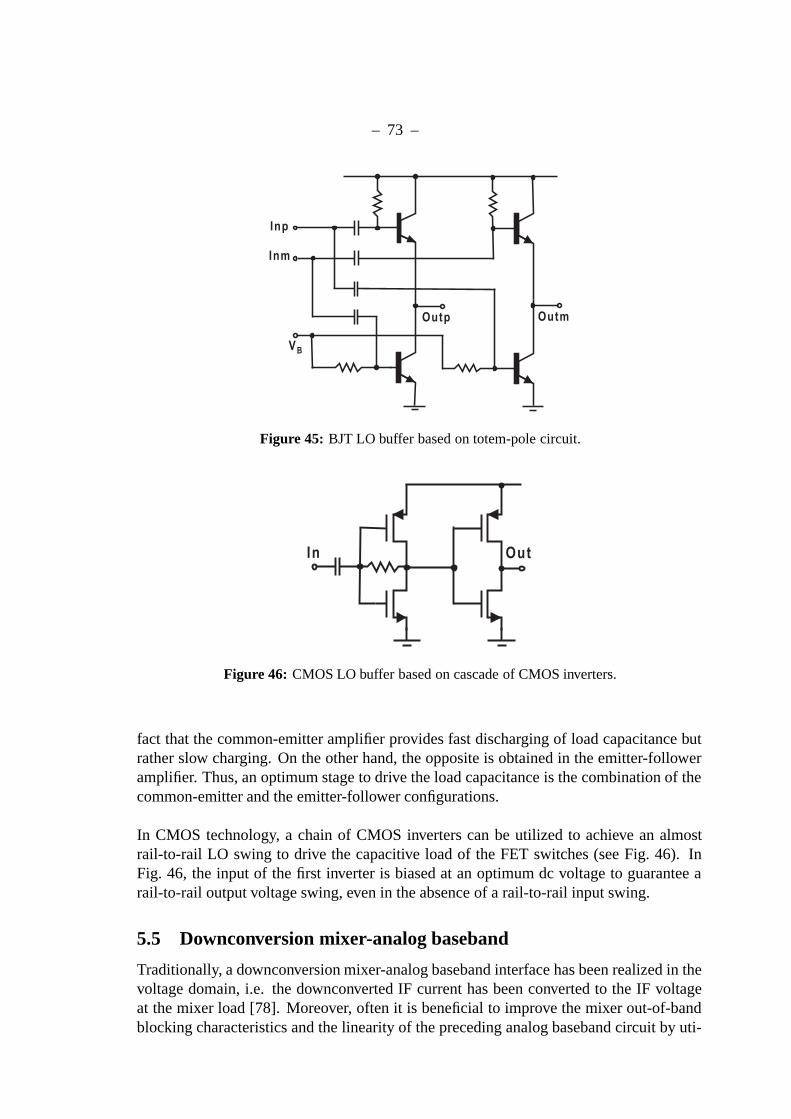
– 73 –
! "
&
#
& #
Figure 45: BJT LO buffer based on totem-pole circuit.
Figure 46: CMOS LO buffer based on cascade of CMOS inverters.
fact that the common-emitter amplifier provides fast discharging of load capacitance butrather slow charging. On the other hand, the opposite is obtained in the emitter-followeramplifier. Thus, an optimum stage to drive the load capacitance is the combination of thecommon-emitter and the emitter-follower configurations.
In CMOS technology, a chain of CMOS inverters can be utilized to achieve an almostrail-to-rail LO swing to drive the capacitive load of the FET switches (see Fig. 46). InFig. 46, the input of the first inverter is biased at an optimum dc voltage to guarantee arail-to-rail output voltage swing, even in the absence of a rail-to-rail input swing.
5.5 Downconversion mixer-analog baseband
Traditionally, a downconversion mixer-analog baseband interface has been realized in thevoltage domain, i.e. the downconverted IF current has been converted to the IF voltageat the mixer load [78]. Moreover, often it is beneficial to improve the mixer out-of-bandblocking characteristics and the linearity of the preceding analog baseband circuit by uti-
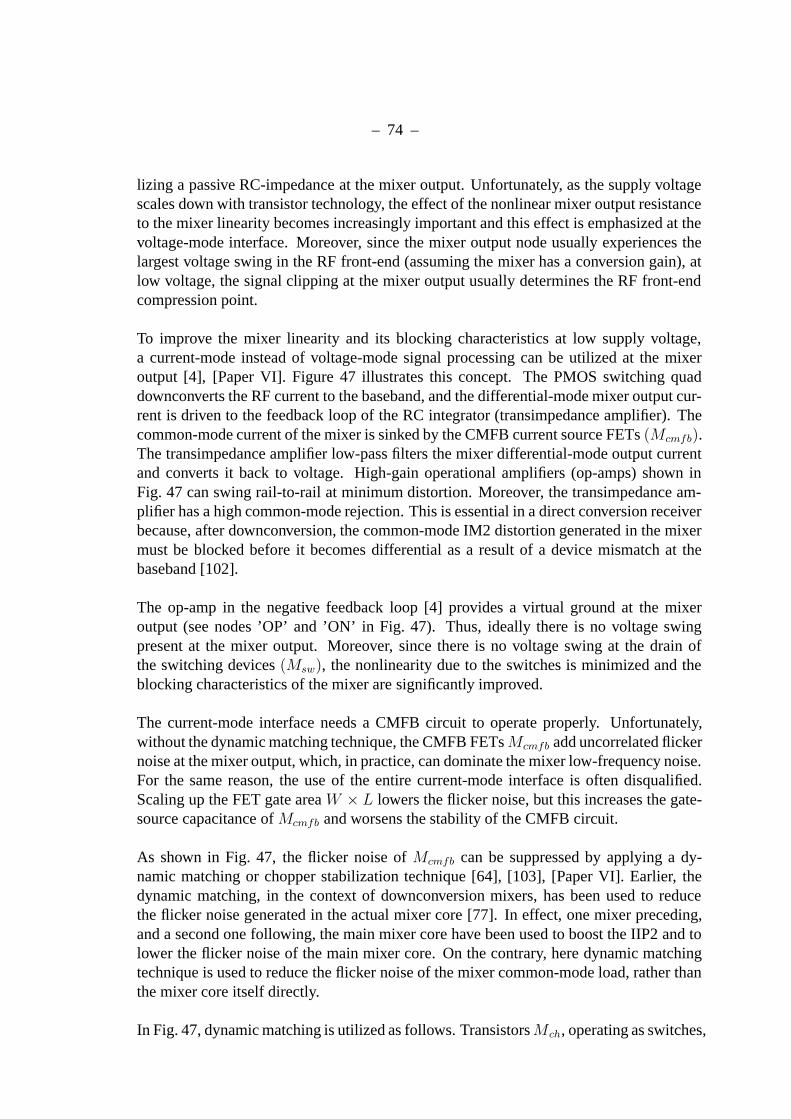
– 74 –
lizing a passive RC-impedance at the mixer output. Unfortunately, as the supply voltagescales down with transistor technology, the effect of the nonlinear mixer output resistanceto the mixer linearity becomes increasingly important and this effect is emphasized at thevoltage-mode interface. Moreover, since the mixer output node usually experiences thelargest voltage swing in the RF front-end (assuming the mixer has a conversion gain), atlow voltage, the signal clipping at the mixer output usually determines the RF front-endcompression point.
To improve the mixer linearity and its blocking characteristics at low supply voltage,a current-mode instead of voltage-mode signal processing can be utilized at the mixeroutput [4], [Paper VI]. Figure 47 illustrates this concept. The PMOS switching quaddownconverts the RF current to the baseband, and the differential-mode mixer output cur-rent is driven to the feedback loop of the RC integrator (transimpedance amplifier). Thecommon-mode current of the mixer is sinked by the CMFB current source FETs (Mcmfb).The transimpedance amplifier low-pass filters the mixer differential-mode output currentand converts it back to voltage. High-gain operational amplifiers (op-amps) shown inFig. 47 can swing rail-to-rail at minimum distortion. Moreover, the transimpedance am-plifier has a high common-mode rejection. This is essential in a direct conversion receiverbecause, after downconversion, the common-mode IM2 distortion generated in the mixermust be blocked before it becomes differential as a result of a device mismatch at thebaseband [102].
The op-amp in the negative feedback loop [4] provides a virtual ground at the mixeroutput (see nodes ’OP’ and ’ON’ in Fig. 47). Thus, ideally there is no voltage swingpresent at the mixer output. Moreover, since there is no voltage swing at the drain ofthe switching devices (Msw), the nonlinearity due to the switches is minimized and theblocking characteristics of the mixer are significantly improved.
The current-mode interface needs a CMFB circuit to operate properly. Unfortunately,without the dynamic matching technique, the CMFB FETsMcmfb add uncorrelated flickernoise at the mixer output, which, in practice, can dominate the mixer low-frequency noise.For the same reason, the use of the entire current-mode interface is often disqualified.Scaling up the FET gate area W × L lowers the flicker noise, but this increases the gate-source capacitance of Mcmfb and worsens the stability of the CMFB circuit.
As shown in Fig. 47, the flicker noise of Mcmfb can be suppressed by applying a dy-namic matching or chopper stabilization technique [64], [103], [Paper VI]. Earlier, thedynamic matching, in the context of downconversion mixers, has been used to reducethe flicker noise generated in the actual mixer core [77]. In effect, one mixer preceding,and a second one following, the main mixer core have been used to boost the IIP2 and tolower the flicker noise of the main mixer core. On the contrary, here dynamic matchingtechnique is used to reduce the flicker noise of the mixer common-mode load, rather thanthe mixer core itself directly.
In Fig. 47, dynamic matching is utilized as follows. TransistorsMch, operating as switches,
– 75 –
- )
4 =
4 #
/
&
&
!
/ 3 2 2 " 1
2 / /
. 3 / >
% ( % (% 3
% ( % (% 3
$ ($ 3
Figure 47: Current-mode downconversion mixer-analog baseband interface.
are driven by rail-to-rail signals vCH+ and vCH− in antiphase at the chopper frequency.Signals vCH+ and vCH− can be generated from the LO signal by a frequency division,and a reasonable choice might be, for instance, fCH = fLO/16 [Paper VI]. Thus, FETsMch essentially form an upconversion mixer, which upconverts the flicker noise of CMFBFETs Mcmfb to the chopper frequency, and therefore outside the signal band of interest.Moreover, since the differential-mode interference signals at the mixer output do not flowthrough the CMFB circuit, the switching quad (Mch) does not downconvert the interfer-ence signals to the signal band of interest. In addition, by driving the switches Mch by alarge amplitude square wave at the relatively low-frequency to a deep triode region, theirvoltage headroom consumption and noise contribution can be made insignificant. Finally,without the dynamic matching, the mismatch in FETs Mcmfb would directly effect theRF front-end IIP2 and dc offset. However, by applying the chopper stabilization, both ofthese effects due to the mismatch in Mcmfb are suppressed. It can also be shown that thedynamic matching has no effect on the white noise contribution of Mcmfb to the mixeroutput noise [Paper VI].
An active filter very often contributes the largest noise of all the building blocks in anintegrated direct conversion receiver [2]. However, the noise contribution of the filter canbe minimized by utilizing a current-mode interface between the downconversion mixerand filter, or by employing a filter with a current-mode input stage (i.e. a transimpedanceamplifier). For instance, if the input-referred noise voltage of the op-amp in the tran-simpedance amplifier shown in Fig. 47 is vn,in, its output noise voltage at the filter pass-band is given as vn,out = (1 +Rp1/Rout,m) × vn,in where Rout,m is the parallel outputimpedance of the mixer and CMFB circuit. If Rp1 << Rout,m then vn,out ≈ vn,in. Thus,

– 76 –
the input-referred noise voltage of the op-amp experiences no voltage gain from the op-amp input to the op-amp output. On the contrary, in a filter with a voltage-mode inputstage, the corresponding noise voltage gain can be significant.
The current-mode interface between the mixer output and analog baseband input is alsovery beneficial regarding to the offset voltage of the op-amp in the transimpedance am-plifier. Similarly, as the input-referred noise voltage, the input-referred offset voltage ofthe op-amp in the transimpedance amplifier experiences no voltage gain to the op-ampoutput. Again, in a filter with a voltage-mode input stage, the corresponding gain can besignificant.
As described above, the differential-mode mixer output current is injected to the feedbackloop of the first RC integrator. Ideally, the differential-mode input impedance (Zin,ta) ofthe transimpedance amplifier should be as small as possible to ensure a maximum transferof current from the mixer output to the transimpedance amplifier output. However, Zin,tais small only in the frequency range where the open loop gain of the op-amp shown inFig. 47 is high [104]. The op-amp must therefore be designed for high-frequency opera-tion. The blocker signals at the frequencies beyond the op-amp gain-bandwidth product(GBW) can be attenuated by the capacitors C1 and C2 at the mixer output. In addition,they prevent the op-amp from slewing due to the high-frequency mixer output signals.Finally, capacitors C2 determine the dominant pole of the CMFB circuit.
As a conclusion, compared to the traditional voltage-mode interface between the down-conversion mixer output and analog baseband input, the current-mode interface improvesthe receiver performance in several ways. Firstly, since there is no voltage swing at themixer output, the nonlinearity due to the mixer switching devices is minimized and themixer blocking performance is improved. The current-mode interface also minimizes thenoise contribution of the analog baseband in such a way that it requires only a moderatevoltage gain (or transconductance) in the LNA and mixer. Both of these issues are veryessential when operating at low supply voltage. Nevertheless, to operate properly, thecurrent-mode interface requires a CMFB circuit. A drawback of a conventional CMFBcircuit is its large flicker noise, which, in practice, can dominate the entire mixer low-frequency noise and prevent the use of the current-mode interface. However, by utilizingthe dynamic matching technique at the interface, the flicker noise of the CMFB circuitcan be suppressed and the use of the entire current-mode interface can be enabled.
– 77 –
6 Summary and Conclusions
In this thesis, the design, analysis, and optimization of RF front-ends for wireless re-ceivers with CMOS and BiCMOS technologies are studied. The research concentrates ondirect conversion and low-IF radio receiver architectures, because typically these receivertopologies allow the highest level of integration. Usually, the RF front-end, especiallythe LNA and mixer, limits the performance of the entire zero- and low-IF receiver. Inthis work, the emphasis is on the challenges posed by mass production to the design ofintegrated RF circuits.
In order to protect the circuits from mechanical stress and to ease the automatic solderingof chips to PCB, commercial RFICs must be mounted in a package and for reliabilityreasons, off-chip interfaces must be protected by ESD protection structures. In the circuitdesign for RF frequencies, the package and ESD parasitics have a significant effect on thecircuit performance and in general, these parasitics do not scale down with technology.In this work, it is shown that the equivalent parallel parasitic capacitance Cp due to theESD and package parasitics drastically lowers the achievable input impedance Zin levelof the inductively degenerated common-emitter (source) LNA, which is the most popu-lar LNA architecture. In order to transform Zin upwards to the source impedance Rs, apassive impedance matching network can be utilized at the amplifier input. However, animpedance matching network with a high impedance scaling factor can make the LNA in-put matching sensitive to process and component variations. The matching network alsoamplifies the incident voltage and lowers the noise contribution due to the active device atthe LNA input. In fact, in an LNA with a sufficiently high device fT and voltage gain inthe matching network, the LNA noise factor can be dominated by the losses of the inputmatching network instead of active device noise. However, very high insertion gain in thematching circuit lowers the IIP3 of the amplifier and may not actually even lead to theminimum achievable noise factor. Instead, the minimum noise factor of the inductivelydegenerated common-source sub-micron LNA can be found when both the matching cir-cuit and the active device at the LNA input contribute an equal amount of noise to theamplifier output.
In order to maximize the yield of receiver RFIC, the circuit performance must be sta-bilized against process, temperature, and supply voltage variations. For this purpose,appropriate circuit techniques and biasing methods must be utilized. Moreover, in orderto reduce the variations of the receiver dynamic range due to the temperature and processvariations, it is shown that it is very important to stabilize the gain of the LNA. In particu-lar, to regulate the voltage gain of the inductively degenerated LNA against variations, themagnitude of the LNA load impedance (|ZL(ω0)|) must be stabilized against variations.To achieve this, a gain stabilization technique for tuned integrated LNAs is proposed inthis thesis. The proposed method is shown to regulate the LC-tuned load impedance ofthe amplifier at the operation frequency against variations of passive devices in the ICprocess. The impedance stabilization technique is based on the excellent relative accu-racy of integrated resistors. By applying the proposed method, the voltage gain variationof the inductively degenerated LNA is shown to be reduced several decibels. As a conse-

– 78 –
quence, the entire radio receiver can more easily meet its specifications in the presence ofIC process variations and the product yield is improved.
One of the most limiting problem in zero- and low-IF receivers is the envelope distor-tion due to the even-order nonlinearity. Usually, in a zero- or low-IF receiver, the mostdominant source of IM2 distortion is the downconversion mixer. Moreover, in generalboth the RF input transconductor and switching devices contribute to the mixer nonlin-earity, and the mixer IIP2 is determined by the mixer second-order nonlinearity, mis-matches, and offsets. As a conclusion, in order to maximize the mixer IIP2, it is essentialto develop techniques for minimizing the IM2 products generated in the mixer, since thedevice matching and offsets cannot be improved beyond certain limits. To enhance theIIP2 of the mixer, a new biasing technique for cancelling the IM2 distortion generated inthe common-source or common-emitter mixer RF input stages is proposed in this thesis.The proposed circuit can be utilized as an RF input transconductor in double-balanceddownconversion mixers. It is shown that the proposed approach increases the yield of theentire radio receiver by enhancing the mixer IIP2. The presented circuit displays ideallyno IM2 distortion, provided that the transconductor is excited differentially and all thetransistors in the circuit match with each other. Moreover, in this circuit, no extra noisesources in practical cases of interest are added in the mixer and no integrated inductorsare required, which results in a small die area. Finally, the presented circuit is also moresuitable for operation at low supply voltage than for instance a conventional differentialpair, because it has only one device stacked between the transconductor input and output.The IIP3 of the proposed circuit is slightly higher than the IIP3 of the differential pair atgiven bias.
Down-scaling of supply voltage with transistor technology poses challenges for the ana-log and RF circuit design. The challenge is how to achieve a large dynamic range andcomply with circuit specifications, which do not relax as the process scales down. Inpractice, low supply voltage limits the upper end of the dynamic range determined by thecircuit’s linearity and prevents stacking of several devices. In addition to low supply volt-age, 1/f noise present in sub-micron CMOS processes is very problematic in the designof direct conversion RF front-ends, especially for narrow-band systems such as GSM.The approach adopted in this study alleviates these problems by utilizing an appropriatedownconversion mixer architecture, i.e. the LC-folded cascode mixer, which providessuperior 1/f noise and linearity performance compared to the other active low-voltagemixers. In addition, compared to the traditional voltage-mode interface, a current-modeinterface between the downconversion mixer output and analog baseband input improvesthe receiver performance in several ways. Firstly, since there is no voltage swing at themixer output, the nonlinearity due to the mixer switching devices is minimized and themixer blocking performance is improved. The current-mode interface also minimizes thenoise contribution of the analog baseband in such a way that it requires only a moder-ate voltage gain (or transconductance) in the LNA and mixer. Both of these issues arevery essential when operating at low supply voltage. Nevertheless, to operate properly,the current-mode interface requires a CMFB circuit. The dynamic matching technique isused to suppress the flicker noise of the CMFB circuit, which otherwise would dominatethe mixer low-frequency noise, and thereby enable the entire current-mode concept.
– 79 –
References
[1] B. Razavi, ”A 900 MHz CMOS direct conversion receiver,” in Symposium on VLSICircuits Digest of Technical Papers, pp. 113-114, 1997.
[2] A. Rofougaran, G. Chang, J. J. Rael, J. Y. C. Chang, M. Rofougaran, P. J. Chang, M.Djafari, J. Min, E. W. Roth, A. A. Abidi, and H. Samueli, ”A single-chip 900-MHzspread-spectrum wireless transceiver in 1-µm CMOS-part II: receiver design,” IEEEJ. Solid-State Circuits, vol. 33, pp. 535-547, Apr. 1998.
[3] A. Parssinen, J. Jussila, J. Ryynanen, L. Sumanen, and K. A. I. Halonen, ”A 2 GHzwide-band direct conversion receiver for WCDMA applications,” IEEE J. Solid-State Circuits, vol. 34, pp. 1893-1903, Dec. 1999.
[4] M. S. J. Steyaert, J. Janssens, B. De Muer, M. Borremans, and N. Itoh, ”A 2-V CMOS cellular transceiver front-end,” IEEE J. Solid-State Circuits, vol. 35,pp. 1895-1907, Dec. 2000.
[5] T. P. Liu and E. Westerwick, ”5-GHz CMOS radio transceiver front-end chipset,”IEEE J. Solid-State Circuits, vol. 35, pp. 1927-1933, Dec. 2000.
[6] R. Magoon, A. Molnar, J. Zachan, G. Hatcher, and W. Rhee, ”A single-chip quad-band (850/900/1800/1900 MHz) direct conversion GSM/GPRS RF transceiver withintegrated VCOs and fractional-N synthesizer,” IEEE J. Solid-State Circuits, vol. 37,pp. 1710-1720, Dec. 2002.
[7] P. van Zeijl, J.-W. T. Eikenbroek, P.-P. Vervoort, S. Setty, J. Tangenberg, G. Shipton,E. Kooistra, I. C. Keestra, D. Belot, K. Visser, E. Bosma, and S. C. Blaakmeer, ”Abluetooth radio in 0.18-µm CMOS,” IEEE J. Solid-State Circuits, vol. 37, pp. 1679-1687, Dec. 2002.
[8] A. A. Abidi, ”RF CMOS comes of age,” IEEE J. Solid-State Circuits, vol. 39,pp. 549-561, April 2004.
[9] F. Behbahani, H. Firouzkouhi, R. Chokkalingam, S. Delshadpour, A. Kheirkhahi,M. Nariman, M. Conta, and S. Bhatia, ”A fully integrated low-IF CMOS GPS radiowith on-chip analog image rejection,” IEEE J. Solid-State Circuits, vol. 37, pp. 1721-1727, Dec. 2002.
[10] L. Perraud, M. Recouly, C. Pinatel, N. Sornin, J.-L. Bonnot, F. Benoist, M. Massei,and O. Gibrat, ”A direct-conversion CMOS transceiver for the 802.11a/b/g WLANstandard utilizing a Cartesian feedback transmitter,” IEEE J. Solid-State Circuits,vol. 39, pp. 2226-2238, Dec. 2004.
[11] E. Duvivier, G. Puccio, S. Cipriani, L. Carpineto, P. Cusinato, B. Bisanti, F. Galant,F. Chalet, F. Coppola, S. Cercelaru, N. Vallespin, J.-C. Jiguet, and G. Sirna, ”Afully integrated zero-IF transceiver for GSM-GPRS quad-band application,” IEEEJ. Solid-State Circuits, vol. 38, pp. 2249-2257, Dec. 2003.
– 80 –
[12] Y.-J. Kim, Y.-S. Son, V. N. Parkhomenko, I.-C. Hwang, J.-K. Cho, K.-S. Nah, andB.-H. Park, ” A GSM/EGSM/DCS/PCS direct conversion receiver with integratedsynthesizer,” IEEE Trans. Microwave Theory Tech., vol. 53, pp. 606-613, Feb. 2005.
[13] E. Duvivier, G. Puccio, S. Cipriani, L. Carpineto, P. Cusinato, B. Bisanti, F. Galant,F. Chalet, F. Coppola, S. Cercelaru, N. Vallespin, J.-C. Jiguet, and G. Sirna, ”Highlyintegrated direct conversion receiver for GSM/GPRS/EDGE with on-chip 84-dBdynamic range continuous-time Σ∆ ADC,” IEEE J. Solid-State Circuits, vol. 40,pp. 403-411, Feb. 2005.
[14] R. Gharpurey, N. Yanduru, F. Dantoni, P. Litmanen, G. Sirna, T. Mayhugh, C. Lin,I. Deng, P. Fontaine, and F. Lin, ”A direct-conversion receiver for the 3G WCDMAstandard,” IEEE J. Solid-State Circuits, vol. 38, pp. 556-560, Mar. 2003.
[15] S. K. Reynolds, B. A. Floyd, T. Beukema, T. Zwick, U. Pfeiffer, and H. Ainspan,”A direct-conversion receiver IC for WCDMA mobile systems,” IEEE J. Solid-StateCircuits, vol. 38, pp. 1555-1560, Sept. 2003.
[16] M. Hafizi, S. Feng, T. Fu, K. Schulze, R. Ruth, R. Schwab, P. Karlsen, D. Simmonds,and G. Qizheng, ”RF front-end of direct conversion receiver RFIC for CDMA-2000,” IEEE J. Solid-State Circuits, vol. 39, pp. 1622-1632, Oct. 2004.
[17] J. Cho, P. Good, M. Kamat, E. McCarthy, K. Rampmeier, W. Cops, A. El Moznine,H. Truong, Y. He, D. Yates, G. Taskov, C.-H. Lee, D. Koh, and S. Lloyd, ”A dual-band tri-mode CDMA IF receiver with programmable channel-match filter,” in Proc.of IEEE RFIC Symposium, Philadelphia, PA, 2003, pp. 391-394.
[18] H. Waite, P. Ta, J. Chen, H. Li, M. Gao, C. S. Chang, Y. S. Chang, W. Redman-White, O. Charlon, Y. Fan, R. Perkins, D. Brunel, E. Soudee, N. Lecacheur, and S.Clamagirand, ”A CDMA2000 zero-IF receiver with low-leakage integrated front-end,” IEEE J. Solid-State Circuits, vol. 39, pp. 1175-1179, Oct. 2004.
[19] A. A. Abidi, ”Direct-conversion radio transceivers for digital communications,”IEEE J. Solid-State Circuits, vol. 30, pp. 1399-1410, Dec. 1995.
[20] F. Behbahani, Y. Kishigami, J. Leete, and A. A. Abidi, ”CMOS mixers andpolyphase filters for large image rejection,” IEEE J. Solid-State Circuits, vol. 36,pp. 873-887, June 2001.
[21] B. Razavi, ”Design considerations for direct-conversion receivers,” IEEE Trans. Cir-cuits Syst. II, vol. 44, pp. 428-435, June 1997.
[22] P. M. Stroet, R. Mohindra, S. Hahn, A. Schuur, and E. Riou, ”A zero-IF single-chiptransceiver for up to 22 Mb/s QPSK 802.11b wireless LAN,” in IEEE ISSCC Dig.Tech. Papers, San Francisco, CA, 2001, pp. 204-205.
[23] W. Kluge, L. Dathe, R. Jaehne, S. Ehrenreich, and D. Eggert, ”A 2.4GHz CMOStransceiver for 802.11b wireless LANs,” in IEEE ISSCC Dig. Tech. Papers, SanFrancisco, CA, 2003, pp. 360-361.
– 81 –
[24] V. Aparin, N. Kim, G. Brown, Y. Wu, A. Cicalini, S. Kwok, and C. Persico, ”A fully-integrated highly linear zero-IF CMOS cellular CDMA receiver,” in IEEE ISSCCDig. Tech. Papers, San Francisco, CA, 2005, pp. 324-326.
[25] J. Rogin, I. Kouchev, G. Brenna, D. Tschopp, and Q. Huang, ”A 1.5-V 45-mWdirect-conversion WCDMA receiver IC 0.13-µm CMOS,” IEEE J. Solid-State Cir-cuits, vol. 38, pp. 2239-2248, Dec. 2003.
[26] S. Dow, B. Ballweber, L.-M. Chou, D. Eickbusch, J. Irwin, G. Kurtzman, P. Man-apragada, D. Moeller, J. Paramesh, G. Black, R. Wollscheid, and K. Johnson,”A dual-band direct-conversion/VLIF transceiver for 50GSM/GSM/DCS/PCS,” inIEEE ISSCC Dig. Tech. Papers, San Francisco, CA, 2002, pp. 230-231.
[27] E. Gotz, H. Krobel, G. Marzinger, B. Memmler, C. Munker, B. Neurauter, D. Romer,J. Rubach, W. Schelmbauer, M. Scholz, M. Simon, U. Steinacker, and C. Stoger, ”Aquad-band low power single chip direct conversion CMOS transceiver with Σ∆-modulation loop for GSM,” in Proc. of the European Solid-State Circuits Confer-ence, Estoril, Portugal, 2003, pp. 217-220.
[28] D. Manstretta, M. Brandolini, and F. Svelto, ”Second-order distortion mechanismsin CMOS downconverters,” IEEE J. Solid-State Circuits, vol. 38, pp. 394-406, Mar.2003.
[29] J. Crols and M. S. J. Steyaert, ”A single-chip 900 MHz CMOS receiver front-endwith a high performance low-IF topology,” IEEE J. Solid-State Circuits, vol. 30,pp. 1483-1492, Dec. 1995.
[30] S. Mahdavi and A. A. Abidi, ”Fully integrated 2.2-mW CMOS front end for a 900-MHz wireless receiver,” IEEE J. Solid-State Circuits, vol. 37, pp. 662-669, May2002.
[31] F. Behbahani, J. C. Leete, Y. Kishigami, A. Roithmeier, K. Hoshino, and A.A. Abidi, ”A 2.4-GHz low-IF receiver for wideband WLAN in 0.6-µm CMOS-architecture and front-end,” IEEE J. Solid-State Circuits, vol. 35, pp. 1908-1916,Dec. 2000.
[32] D. K. Shaeffer, A. R. Shahani, S. S. Mohan, H. Samavati, H. R. Rategh, M. del MarHershenson, M. Xu, C. P. Yue, D. J. Eddleman, and T. H. Lee, ”A 115-mW, 0.5-µmCMOS GPS receiver with wide dynamic-range active filters,” IEEE J. Solid-StateCircuits, vol. 33, pp. 2219-2231, Dec. 1998.
[33] A. J. Scholten, L. F. Tiemeijer, R. van Langevelde, R. J. Havens, A. T. A. Zegers-vanDuijnhoven, and V. C Venezia, ”Noise modeling for RF CMOS circuit simulation,”IEEE Trans. Electron Devices, vol. 50, pp. 618-632, Mar. 2003.
[34] G. Gramegna, M. Paparo, P. G. Erratico, and P. De Vita, ”A sub-1-dB ±2.3-kV ESD-protected 900-MHz CMOS LNA,” IEEE J. Solid-State Circuits, vol. 36, pp. 1010-1017, July 2001.
– 82 –
[35] H. Darabi and A. A. Abidi, ”A 4.5-mW 900-MHz CMOS receiver for wireless pag-ing,” IEEE J. Solid-State Circuits, vol. 35, pp. 1085-1096, Aug. 2000.
[36] A. A. Abidi, G. J. Pottie, and W. J. Kaiser, ”Power-conscious design of wirelesscircuits and systems,” in Proc. of IEEE, vol. 88, pp. 1528-1545, Oct. 2000.
[37] P. R. Gray and R. G. Meyer, Analysis and Design of Analog Integrated Circuits,John Wiley and Sons, 1993.
[38] R. G. Meyer and W. D. Mack, ”A 1-GHz BiCMOS RF-front-end integrated circuit,”IEEE J. Solid-State Circuits, vol. 29, pp. 350-355, Mar. 1994.
[39] T. H. Lee, The Design of CMOS Radio-Frequency Integrated Circuits, CambridgeUniversity Press, 1998.
[40] B. Razavi, RF Microelectronics, Prentice Hall PTR, 1998.
[41] H. Darabi and A. A. Abidi, ”Noise in RF-CMOS mixers: A simple physical model,”IEEE J. Solid-State Circuits, vol. 35, pp. 15-25, Jan. 2000.
[42] K. Kivekas, A. Parssinen, and K. A. I. Halonen, ”Characterization of IIP2 and DC-offsets in transconductance mixers,” IEEE Trans. Circuits Syst. II, vol. 48, pp. 1028-1038, Nov. 2001.
[43] A. Matsuzawa, ”RF-SoC-Expectations and required conditions,” IEEE Trans. Mi-crowave Theory Tech., vol. 50, pp. 245-253, Jan. 2002.
[44] T. Manku, G. Beck, and E. J. Shin, ”A low-voltage design technique for RF inte-grated circuits,” IEEE Trans. Circuits Syst. II, vol. 45, pp. 1408-1413, Oct. 1998.
[45] O. E. Erdogan, R. Gupta, D. G. Yee, J. C. Rudell, J. S. Ko, R. Brockenbrough, S. O.Lee, E. Lei, J. L. Tham, H. Wu, C. Conroy, and B. Kim, ”A single-chip quad-bandGSM/GPRS transceiver in 0.18µm standard CMOS,” in IEEE ISSCC Dig. Tech.Papers, San Francisco, CA, 2005, pp. 318-319.
[46] A. Rofougaran, J. Y. C. Chang, M. Rofougaran, and A. A. Abidi, ”A 1 GHz CMOSRF front-end IC for a direct-conversion wireless receiver,” IEEE J. Solid-State Cir-cuits, vol. 31, pp. 880-889, July 1996.
[47] H. T. Fris, ”Noise figures of radio receivers,” in Proc. of IRE, vol. 32, pp. 419-422,July 1944.
[48] B. Razavi, ”A 2.4-GHz CMOS receiver for IEEE 802.11 wireless LAN’s,” IEEE J.Solid-State Circuits, vol. 34, pp. 1382-1385, Oct. 1999.
[49] K. L. Fong, C. D. Hull, and R. G. Meyer, ”A class AB monolithic mixer for 900-MHz applications,” IEEE J. Solid-State Circuits, vol. 32, pp. 1166-1172, Aug. 1997.
[50] K. Kivekas, ”Design and characterization of downconversion mixers and the on-chip calibration techniques for monolithic direct conversion radio receivers,” Ph.D.Dissertation, Helsinki University of Technology, Espoo, Finland, 2002.

– 83 –
[51] H. Sjoland, A. Kamiri-Sanjaani, and A. A. Abidi, ”A merged CMOS LNA and mixerfor a WCDMA receiver,” IEEE J. Solid-State Circuits, vol. 38, pp. 1045-1050, June2003.
[52] F. Gatta, D. Manstretta, P. Rossi, and F. Svelto, ”A fully integrated 0.18-µm CMOSdirect conversion receiver front-end with on-chip LO for UMTS,” IEEE J. Solid-State Circuits, vol. 38, pp. 15-23, Jan. 2004.
[53] M. Brandolini, P. Rossi, D. Manstretta, and F. Svelto, ”Toward multistandard mobileterminals-fully integrated receivers requirements and architectures,” IEEE Trans.Microwave Theory Tech., vol. 53, pp. 1026-1038, Mar. 2005.
[54] D. K. Shaeffer and T. H. Lee, ”A 1.5-V, 1.5-GHz CMOS Low Noise Amplifier,”IEEE J. Solid-State Circuits, vol. 32, pp. 745-759, May 1997.
[55] G. Girlando and G. Palmisano, ”Noise figure and impedance matching in RF cas-code amplifiers,” IEEE Trans. Circuits Syst. II, vol. 46, pp. 1388-1396, Nov. 1999.
[56] P. Rossi, A. Liscidini, M. Brandolini, and F. Svelto, ”A variable gain RF front-end,based on a voltage-voltage feedback LNA, for multistandard applications,” IEEE J.Solid-State Circuits, vol. 40, pp. 690-697, Mar. 2005.
[57] B. A. Floyd, J. Mehta, C. Camero, and K. K. O, ”A 900-MHz, 0.8µm CMOS lownoise amplifier with 1.2-dB noise figure,” in Proc. Custom Integrated Circuits Conf.,1999, pp. 661-664.
[58] P. Andreani and H. Sjoland, ”Noise optimization of an inductively degeneratedCMOS low noise amplifier,” IEEE Trans. Circuits Syst. II, vol. 48, pp. 835-841,Sept. 2001.
[59] T. K. Nguyen, C. H. Kim, G. J. Ihm, M. S. Yang, and S. G. Lee, ”CMOS low-noiseamplifier design optimization techniques,” IEEE Trans. Microwave Theory Tech.,vol. 52, pp. 1433-1442, May 2004.
[60] P. Leroux and M. Steyaert, ”High-performance 5.2GHz LNA with on-chip inductorto provide ESD protection,” Electron. Lett., vol. 37, pp. 467-469, Mar. 2001.
[61] P. Leroux, J. Janssens, and M. Steyaert, ”A 0.8-dB NF ESD-protected 9-mW CMOSLNA operating at 1.23 GHz,” IEEE J. Solid-State Circuits, vol. 37, pp. 760-765, June2002.
[62] J. Chang, “An integrated 900 MHz spread-spectrum wireless receiver in 1-µmCMOS and a suspended inductor technique”, Ph.D. Thesis, UCLA, Mar. 1998.
[63] V. Chandrasekhar and K. Mayaram, ”Analysis of CMOS RF LNAs with ESD pro-tection,” in IEEE Int. Circuits and Systems Symp., 2002, pp. 779-802.
[64] P. E. Allen and D. R. Holberg, CMOS Analog Circuit Design, Saunders CollegePublishing, 1987.
– 84 –
[65] R. T. Chang, M. T. Yang, P. P. C. Ho, Y. J. Wang, Y. T. Chia, B. K. Liew, C. P. Yue,and S. S. Wong, ”Modeling and optimization of substrate resistance for RF-CMOS,”IEEE Trans. Electron Devices, vol. 51, pp. 421-426, Mar. 2004.
[66] W. Guo and D. Huang, ”Noise and linearity analysis for a 1.9GHz CMOS LNA,” inProc. Asia-Pacific Circuits and Systems Conf., 2002, pp. 409-414.
[67] A. Vilander and P. Sivonen, ”Gain stabilization technique for narrow band integratedlow noise amplifiers,” U.S. Patent no. 6963247, Nov. 2005.
[68] J. Ryynanen, K. Kivekas, J. Jussila, A. Parssinen, and K. Halonen, ”RF gain controlin direct conversion receivers,” in IEEE Int. Circuits and Systems Symp., Scottsdale,Arizona, 2002, pp. 117-120.
[69] J. Ryynanen, ”Low-noise amplifiers for integrated multi-mode direct-conversion re-ceivers,” Ph.D. Dissertation, Helsinki University of Technology, Espoo, Finland,2004.
[70] J. Ryynanen, K. Kivekas, J. Jussila, A. Parssinen, and K. A. I. Halonen, ”A dual-band RF front-end for a WCDMA and GSM applications,” IEEE J. Solid-State Cir-cuits, vol. 36, pp. 1198-1204, Aug. 2001.
[71] S. Tadjpour, E. Cijvat, E. Hegazi, and A. A. Abidi, ”A 900-MHz dual-conversionlow-IF GSM receiver in 0.35-µm CMOS,” IEEE J. Solid-State Circuits, vol. 36,pp. 1992-2002, Dec. 2001.
[72] K. L. Fong, ”Dual-band high-linearity variable-gain low-noise amplifiers for wire-less applications,” in IEEE ISSCC Dig. Tech. Papers, San Francisco, CA, 1999,pp. 224-225.
[73] H. Darabi, S. Khorram, Z. Zhou, T. Li, B. Marholev, J. Chiu, J. Castaneda, E. Chien,S. Anand, S. Wu, M. Pan, R. Rofougaran, H. Kim, P. Lettieri, B. Ibrahim, J. Rael,L. Tran, E. Geronaga, H. Yeh, T. Frost, J. Trachewsky, and A. Rofougaran, ”A fullyintegrated SoC for 802.11b in 0.18µm CMOS,” in IEEE ISSCC Dig. Tech. Papers,San Francisco, CA, 2005, pp. 96-97.
[74] A. Zolfaghari and B. Razavi, ”A low-power 2.4-GHz transmitter/receiver CMOSIC,” IEEE J. Solid-State Circuits, vol. 38, pp. 176-183, Feb. 2003.
[75] F. Behbahani, Y. Kishigami, J. Leete, and A. A. Abidi, ”CMOS mixers andpolyphase filters for large image rejection,” IEEE J. Solid-State Circuits, vol. 36,pp. 873-886, June 2001.
[76] K. L. Fong and R. G. Meyer, ”Monolithic RF active mixer design,” IEEE J. Solid-State Circuits, vol. 46, pp. 231-239, Mar. 1999.
[77] E. E. Bautista, B. Bastani, and J. Heck, ”A high IIP2 downconversion mixer usingdynamic matching,” IEEE J. Solid-State Circuits, vol. 35, pp. 1934-1941, Dec. 2000.
– 85 –
[78] B. Gilbert, ”The MICROMIXER: A highly linear variant of the Gilbert mixer usinga bisymmetric class-AB input stage,” IEEE J. Solid-State Circuits, vol. 32, pp. 1412-1423, Sep. 1997.
[79] W. Sansen, ”Distortion in elementary transistor circuits,” IEEE Trans. Circuits Syst.II, vol. 46, pp. 315-325, Mar. 1999.
[80] K. L. Fong and R. G. Meyer, ”High-frequency nonlinearity analysis of common-emitter and differential-pair transconductance stages,” IEEE J. Solid-State Circuits,vol. 33, pp. 548-555, Apr. 1998.
[81] M. T. Terrovitis and R. G. Meyer, ”Noise in current-commutitating CMOS mixers,”IEEE J. Solid-State Circuits, vol. 34, pp. 772-783, June 1999.
[82] V. Vidojkovic, J. van der Tang, A. Leeuwenburg, and A. H. M. van Roermund,”A low-voltage folded-switching mixer in 0.18-µm CMOS,” IEEE J. Solid-StateCircuits, vol. 40, pp. 1259-1264, June 2005.
[83] H. Darabi and J. Chiu, ”A noise cancellation technique in active RF-CMOS mixers,”in IEEE ISSCC Dig. Tech. Papers, San Francisco, CA, 2005, pp. 544-545.
[84] D. Manstretta, R. Castello, and F. Svelto, ”Low 1/f noise CMOS active mixers fordirect conversion,” IEEE Trans. Circuits Syst. II, vol. 48, pp. 846-850, Sep. 2001.
[85] Z. Xu, S. Jiang, Y. Wu, H. Jian, G. Chu, K. Ku, P. Wang, N. Tran, Q. Gu, M.Lai, C. Chien, M. Chang, and P. Chow, ”A compact dual-band direct-conversionCMOS transceiver for 802.11a/b/g WLAN,” in IEEE ISSCC Dig. Tech. Papers, SanFrancisco, CA, 2005, pp. 98-99.
[86] E. Abou-Allam, J. J. Nisbet, and M. C. Maliepaard, ”Low-voltage 1.9-GHz front-end receiver in 0.5-µm CMOS technology,” IEEE J. Solid-State Circuits, vol. 36,pp. 1434-1442, Oct. 2001.
[87] T. W. Kim, B. Kim, and K. Lee, ”Highly linear receiver front-end adopting MOSFETtransconductance linearization by multiple gated transistors,” IEEE J. Solid-StateCircuits, vol. 39, pp. 223-229, Jan. 2004.
[88] D. Coffing and E. Main, ”Effects of offsets on bipolar integrated circuit even-orderdistortion terms,” IEEE Trans. Microwave Theory Tech., vol. 49, pp. 23-30, Jan.2001.
[89] A. A. Abidi, ”General relations between IP2, IP3, and offsets in differential cir-cuits and the effects of feedback,” IEEE Trans. Microwave Theory Tech., vol. 51,pp. 1610-1612, May 2003.
[90] S. Wu and B. Razavi, ”A 900-MHz/1.8-GHz CMOS receiver for dual-band applica-tions,” IEEE J. Solid-State Circuits, vol. 33, pp. 2178-2185, Dec. 1998.
– 86 –
[91] A. Vilander and P. Sivonen, ”Method and apparatus providing cancellation of sec-ond order intermodulation distortion and enhancement of second order interceptpoint (IIP2) in common source and common emitter transconductance circuits,” U.S.Patent no. 6992519, Jan. 2006.
[92] M. Brandolini, P. Rossi, D. Sanzogni, and F. Svelto, ”A CMOS direct down-converter with +78dBm minimum IIP2 for 3G cell-phones,” in IEEE ISSCC Dig.Tech. Papers, San Francisco, CA, 2005, pp. 320-321.
[93] T. H. Lee, The Design of CMOS Radio-Frequency Integrated Circuits, CambridgeUniversity Press, 1998.
[94] P. Wambacq and W. Sansen, Distortion Analysis of Analog Integrated Circuits,Kluwer Academic Publishers, 1998.
[95] C. C. Enz and E. A. Vittoz, ”CMOS low-power analog circuit design,” DesigningLow Power Digital Systems, Emerging Technologies (1996), 1996, pp. 79-133.
[96] K. Kivekas, A. Parssinen, J. Ryynanen, J. Jussila, and K. Halonen, ”Calibrationtechniques of active BiCMOS mixers,” IEEE J. Solid-State Circuits, vol. 37, pp. 766-769, June 2002.
[97] M. Hotti, J. Ryynanen, K. Kivekas, and K. Halonen, ”An IIP2 calibration techniquefor direct conversion receivers,” in Proc. of ISCAS Symposium, Vancouver, Canada,2004, pp. 257-260.
[98] A. Rofougaran, G. Chang, J. J. Rael, J. Y. C. Chang, M. Rofougaran, P. J. Chang,M. Djafari, M. K. Ku, E. W. Roth, A. A. Abidi, and H. Samueli, ”A single-chip 900-MHz spread-spectrum wireless transceiver in 1-µm CMOS-part I: Architecture andtransmitter design,” IEEE J. Solid-State Circuits, vol. 33, pp. 515-534, Apr. 1998.
[99] H. Darabi, S. Khorram, H.-M. Chien, M. Pan, S. Wu, S. Moloudi, J. C. Leete, J. J.Rael, M. Syed, R. Lee, B. Ibrahim, M. Rofougaran, and A. Rofougaran, ”A 2.4-GHzCMOS transceiver for bluetooth,” IEEE J. Solid-State Circuits, vol. 36, pp. 2016-2024, Dec. 2001.
[100] E. Song, Y. Koo, Y.-J. Jung, D.-H. Lee, S. Chu, and S.-I. Chae, ”A 0.25-µm CMOSquad-band GSM RF transceiver using an efficient LO frequency plan,” IEEE J.Solid-State Circuits, vol. 40, pp. 1094-1106, May 2005.
[101] A. S. Sedra and K. C. Smith, Microelectronic Circuits, Saunders College Publish-ing, 1991.
[102] J. Ryynanen, K. Kivekas, J. Jussila, L. Sumanen, A. Parssinen, and K. A. I. Halo-nen, ”A single-chip multimode receiver for GSM900, DCS1800, PCS1900, andWCDMA,” IEEE J. Solid-State Circuits, vol. 38, pp. 594-602, Apr. 2003.
[103] J-P. Tervaluoto, A. Ruha, and T. Ruotsalainen, ”Mixer circuit,” U.S. patent appli-cation, January 2004.

– 87 –
[104] E. Sacchi, I. Bietti, S. Erba, L. Tee, P. Vilmercati, and R. Castello, ”A 15 mW,70 kHz 1/f corner direct conversion CMOS receiver,” in Proc. Custom IntegratedCircuits Conf., San Jose, CA, 2003, pp. 459-462.

– 88 –
Abstracts of Publications I-VI
I. This paper presents an RF front-end with on-chip VCO fabricated in 0.35-µm SiGeBiCMOS technology for a direct conversion GPS receiver. The circuit design ofpackaged inductively degenerated common-emitter LNA with ESD protection isdescribed, and theoretically calculated LNA performance is compared with simu-lations. The DSB-NF and IIP3 of the resistively degenerated Gilbert-type down-conversion mixer are analyzed, and theoretically estimated mixer performance iscompared with simulations. The approximative equations describing the entire RFfront-end DSB-NF and IIP3 are also given. By applying the derived formulas, thefront-end performance can be readily estimated and optimized. The implementedRF front-end achieves low noise (DSB-NF of 2.7 dB @ 1.575 GHz) at low powerconsumption (15.3 mA from a 2.7 V supply).
II. In this paper, the effects of packaging and ESD protection on the performance ofinductively degenerated common-emitter LNA are examined and the equations de-scribing the input impedance, transconductance, voltage gain, and NF of the pack-aged amplifier are derived. From the equations several guidelines for the LNAdesign are obtained and a systematic approach for the LNA design can be derived.Furthermore, by applying the formulas, the performance of the amplifier can bereadily estimated and optimized in the very early stage of the circuit design, imme-diately as the process data is available. It is concluded that the equivalent parallelparasitic capacitance (Cp) due to the package and ESD parasitics limits the achiev-able impedance level at the LNA input and it lowers the noise contributions of theLNA input circuit (i.e. base resistance and base shot noise) to the LNA NF. Themeasurement results of the implemented 0.35-µm SiGe RF front-end with induc-tively degenerated common-emitter LNA are found to agree well with theoreticalcalculations and simulations.
III. A gain stabilization technique for tuned integrated LNAs is presented in this pa-per. The proposed method is shown to regulate the magnitude of the LC-tuned loadimpedance of the amplifier at the operation frequency against variations of passivedevices in the IC process. The impedance stabilization technique is based on the ex-cellent relative accuracy of integrated resistors. Although the absolute deviation ofthe integrated resistors can be as large as ±20%, the relative deviation can be madesmaller than ±1% provided that resistors are placed close to each other. In the pa-per, the design equations for the gain stabilization technique are derived and thenecessary conditions for the method to operate properly are presented. By applyingthe proposed method, the voltage gain variation of the inductively degenerated LNAis shown to be reduced several decibels. As a consequence, the entire radio receivercan more easily meet its specifications in the presence of IC process variations andthe product yield is improved. Finally, besides of the LNAs, the presented stabi-lization technique can also be utilized in other tuned amplifiers, filters or oscillatorsemploying damped LC-tuned loads.
– 89 –
IV. In this paper, the effects of packaging in inductively degenerated common-sourceLNAs with ESD protection are studied and the performance of the packaged LNAis optimized. Equations describing the input impedance, transconductance, voltagegain, and NF of the packaged amplifier are derived and the effects of the LNA inputmatching network, package, and ESD parasitics on these amplifier quantities arehighlighted. From the equations, several design guidelines for the packaged LNAare obtained and a systematic approach for the ESD-protected LNA optimizationis deduced. It is also shown that in the presence of an equivalent parallel packageparasitic capacitance (Cp), the NF in a well-optimized LNA is easily dominated bythe losses of the input matching network, instead of active device noise. Based onthe theoretical results, a packaged inductively degenerated common-source LNAwith ESD protection is designed in the 0.13 µm CMOS process. The amplifierachieves a low NF of 1.6 dB at 2 GHz while consuming 8.4 mW from a 1.2 Vsupply.
V. In this paper, a biasing technique for cancelling second-order intermodulation (IM2)distortion and enhancing IIP2 in common-source and common-emitter RF transcon-ductors is presented. The proposed circuit can be utilized as an RF input transcon-ductor in double-balanced downconversion mixers. It is shown that the proposedapproach increases the yield of the entire radio receiver by enhancing the mixerIIP2. The presented circuit displays ideally no IM2 distortion provided that thetransconductor is excited differentially and all the transistors in the circuit matchwith each other. Moreover, in this circuit, no extra noise sources in practical casesof interest are added in the mixer and no integrated inductors are required, whichresults in a small die area. Finally, the presented transconductor is also suitable foroperation at low supply voltages, because it has only one device stacked betweenthe transconductor input and output. The IIP3 of the proposed transconductor isslightly higher than the IIP3 of the differential pair transconductor at given bias.In the paper, the operation principle of the proposed transconductor is explainedand analyzed by direct calculation of the nonlinear responses and the nonidealitiesof the transconductor are discussed. The theoretical analysis is also verified withexperimental circuit simulations and the proposed transconductor is simulated as apart of the complete downconversion mixer.
VI. In this paper, a 1.2-V RF front-end realized for a PCS direct conversion receiver ispresented. The RF front-end comprises an LNA, quadrature mixers, and active RClow-pass filters with gain control. Quadrature LO signals are generated on chip bya double-frequency VCO and frequency divider. A current-mode interface betweenthe downconversion mixer output and analog baseband input, together with a dy-namic matching technique, is shown to simultaneously improve the mixer linearity,lower the flicker noise due to the mixer switches, and minimize the noise contribu-tion of the analog baseband. The dynamic matching technique is employed to sup-press the flicker noise of the CMFB circuit utilized at the mixer output, which oth-erwise would dominate the low-frequency noise of the mixer. Various low-voltagecircuit techniques are employed to enhance both the mixer second- and third-orderlinearity, and to lower the flicker noise. The RF front-end is fabricated in a 0.13-µmCMOS process utilizing only standard process options.

ISBN 951-22-8366-2ISBN 951-22-8367-0 (PDF)ISSN 1795-2239ISSN 1795-4584 (PDF)