Embed Size (px)
Citation preview

Depth resolved investigation of ion beam induced
pattern formation on silicon using X-ray methods
DISSERTATION
zur Erlangung des Grades eines Doktors
der Naturwissenschaften
vorgelegt von
M. Sc. Behnam Khanbabaee Patekhour
eingereicht bei der Naturwissenschaftlich-Technischen Fakultät
der Universität Siegen
Siegen 2014

Gutachter: Prof. Dr. Dr. h.c. Ullrich Pietsch
Prof. Dr. Dr. h.c. Bernd Rauschenbach
Prüfer: Prof. Dr. Hans Dieter Dahmen
Prof. Dr. Christian Gutt
Tag der mündlichen Prüfung: 30.04.2014

i
Abstract
In the present work, ion beam induced pattern formation on silicon surfaces is investigated,
which was induced by off-normal irradiation of Fe ions. It is observed that the self-organized
surface patterning takes place when the ion fluence exceeds a certain limit. The influence of the
ion parameters on the patterning mechanism was investigated via monitoring of the near surface
area where incorporated Fe ions play a dominant role.
In a first step, ion beam induced surface density variation was studied as a function of ion
parameters. Conventional X-ray reflectivity revealed the formation of a nm sub-surface layer
with incorporated Fe atoms. Using X-ray reflectivity, no major dependence of the surface density
on the ion fluence could be obtained. Thus, a new powerful technique with higher surface
sensitivity was applied based on extremely asymmetrical X-ray diffraction methods. The density
information was extracted from the shift of the diffraction peak caused by refraction of the X-ray
beam at the air-sample interface. Simulations based on the dynamical theory of X-ray diffraction
revealed a decrease of the density for increasing ion fluence in a region close to the surface. It
shows that there is a threshold value for ion fluence leading to reduction of surface density. The
obtained results reveal that the change of local density contributes to the development of the
pattern on the surface.
In a second step, Fe-silicide formation in various stoichiometries was investigated in the
amorphized surface region of crystalline Si(100) after irradiation with Fe ions. A depth resolved
analysis of chemical states of Si and Fe atoms in the near surface region was performed by
combining X-ray photoelectron spectroscopy and X-ray absorption spectroscopy using
synchrotron radiation. The formation of silicide bonds of different stoichiometric composition
changing from an Fe-rich silicide (Fe3Si) close to the surface into a Si-rich silicide (FeSi2)
towards to the inner interfaces was observed. This observation shows that the presence of
chemically bonded iron close to the surface is an important prerequisite of pattern formation.
In a third step, the recrystallization of the pre-formed Fe-silicides of various stoichiometries
was investigated below the amorphized surface of crystalline Si(100). A thermal annealing
process was applied in the range between room temperature and 800°C. Depth profiling by
grazing incidence X-ray diffraction confirmed that a ε-FeSi phase was formed close to the surface
changing to a -FeSi2 phase with lower Fe content at larger depths. Both phases are distributed

ii
with different ratios within the Fe-Si layer at smooth and patterned surfaces, corresponding to
low and high ion fluences, respectively.
In the last step, the obtained results were examined for pattern formation on Si(001) surfaces
under normal incident Kr ion bombardment with simultaneous incorporation of Fe atoms. It was
verified that the surface patterning takes place only when the incorporated Fe concentration again
exceeds a certain limit. For a high Fe concentration the ripple formation is accompanied by the
enrichment of Fe atoms at the top part of ripples, whereas no such Fe enhancement is found for a
low Fe concentration at samples with smooth surfaces. Modeling of the measured X-ray
photoelectron spectroscopy and X-ray absorption spectroscopy spectra reveals the appearance of
different silicide phases with a decreasing Fe content from top towards the volume.
Abstract

iii
Zusammenfassung
In der vorliegenden Arbeit wird die Musterbildung auf Siliziumoberflächen durch den Beschuss
mit Eisenionen unter schrägem Einfallswinkeln untersucht. Experimentell wird beobachtet, dass
es zu selbstorganisierter Strukturbildung an der Oberfläche kommt, wenn die Ionendosis (Fluenz)
einen bestimmten Schwellenwert überschreitet. In dieser Arbeit wird der Einfluss der
Ionenstrahl-Parameter auf die Musterbildung untersucht. Insbesondere wird die Region nahe der
Oberfläche, in welcher die Fe-Ionen eine entscheidende Rolle bei der Musterbildung spielen,
mittels Oberflächensensitiver Röntgenstreuung untersucht.
In einem ersten Schritt wird das Dichteprofil nahe der Oberfläche als Funktion von
Ionenenergie und Fluenz untersucht. Röntgenreflektometrie zeigt dabei die Ausbildung eine mit
Eisen angereicherten Schicht in den ersten Nanometern unterhalb der Oberfläche, jedoch wird
keine ausgeprägte Abhängigkeit von der Ionenfluenz festgestellt.
Um die Oberflächensensitivität weiter zu erhöhen, wird eine neue Methode basierend auf der
extrem asymmetrischen Röntgenbeugung eingesetzt. Diese erlaubt die Ermittelung kleinster
Dichtevariationen infolge des Nachweises kleinster Winkelverschiebungen des gebeugten
Röntgenstrahls auf Grund der Brechung des Röntgenstrahls an der Oberfläche. Durch
Simulationen mit Hilfe der dynamischen Theorie der Röntgenbeugung wird eine mit steigender
Fluenz zunehmende Verringerung der Dichte nahe der Oberfläche nachgewiesen. Daraus wird
gefolgert, dass die Massendichte an der Oberfläche unter Einfluss der Musterbildung abnimmt.
In einem zweiten Schritt wird die Ausbildung von Eisen-Siliziden verschiedener
Stöchiometrie in der amorphisierten Region nahe der Oberfläche untersucht. Die Kombination
von Röntgen-Photoemissions-Spektroskopie und Röntgenabsorptionsspektroskopie mittels
Synchrotronstrahlung erlaubt eine tiefenaufgelöste Bestimmung der chemischen
Bindungszustände von Si und Fe atomen nahe der Oberfläche. Es wird gezeigt, dass sich nahe
der Oberfläche Eisenreiches Silizid (Fe3Si), in größerer Tiefe nahe der Grenzsschicht zu noch
kristallinem Silizium jedoch vermehrt Siliziumreiches FeSi2 Silizid bilded. Dieser Nachweis
belegt, dass chemisch gebundenes Eisen eine Vorbedingung zur Musterbildung darstellt. Die
gebildeten Phasen mit unterschiedlichem Fe-Si Verhältnis auf glatten und strukturierten
Oberflächen entsprechen niedrigen und hohen Ionen Flüssen.

iv
In einem dritten Schritt wird die Rekristallisation dieser Eisensilizide während thermischem
Ausheizens bei Temperaturen bis 800°C untersucht. Tiefenaufgelöste Messungen mittels
Röntgenbeugung unter streifendem Einfall (GID) belegen, dass sich nahe der Oberfläche ε-FeSi
bildet, in größerer Tiefe jedoch -FeSi2 mit geringerem Fe-Gehalt. Verschiedene gebildeten
Phasen mit unterschiedlichen Verhältnis im Fe-Si Schicht auf glatten und strukturierten
Oberflächen entsprach niedrige und hohe Ionen Flüssen.
Zuletzt wird die Musterbildung auf Si(001) Oberflächen nach Krypton-Sputtering bei
gleichzeitigem Eisen-Eintrag untersucht. Es zeigt sich, dass es auch in diesem Fall nur zu
Musterbildung kommt, wenn die Konzentration von Eisenatomen an der Oberfläche einen
Schwellenwert überschreitet. Für hohe Eisenkonzentrationen kommt es zur Ausbildung
periodischer Ripple-Muster mit einer Anreicherung von Eisen nahe der „Gipfel“ der Ripples.
Photoelektronen-Spektroskopie und Röntgenabsorptionsspektroskopie zeigen auch hier die
Ausbildung von Silizidphasen mit abnehmendem Eisengehalt von der Oberfläche in Richtung auf
das Volumen.
Zusammenfassung

v
Contents
1 Introduction .................................................................................................................. 1
2 Ion beam induced pattern formation ........................................................................... 5
2.1 Ion-solid interaction process.................................................................................................. 5
2.2 Theoretical approaches in surface morphology modulation .................................................. 7
2.3 Bradley and Harper linear instability model........................................................................ 10
2.4 Patterning by ion bombardment with co-deposition of impurities ...................................... 11
3 Surface and interface characterization methods ......................................................13
3.1 Refraction and reflection of X-rays from interfaces ............................................................ 13
3.2 X-ray diffraction theories .................................................................................................... 17
3.2.1 Kinematical theory .......................................................................................................... 17
3.2.2 Dynamical theory ............................................................................................................ 23
3.3 Experimental realization ...................................................................................................... 31
3.3.1 Surface sensitive extremely asymmetrical X-ray diffraction ......................................... 35
3.4 X-ray absorption methods ................................................................................................... 40
3.4.1 X-ray Photoelectron spectroscopy .................................................................................. 42
3.4.2 X-ray absorption spectroscopy ....................................................................................... 45
3.5 Experimental procedure....................................................................................................... 51
4 Pattern formation on direct off-normal Fe ion irradiated Si(100) surfaces ..............59
4.1 Sample preparation .............................................................................................................. 59

vi
4.2 Surface and interface morphology analysis ......................................................................... 60
4.3 Depth density profiling of Si(100) after irradiation with Fe ions ........................................ 69
4.3.1 X-ray reflectivity ............................................................................................................. 69
4.3.2 Extremely asymmetric diffraction with changing scattering geometry ........................... 72
4.3.3 Extremely asymmetric diffraction with changing the wavelength .................................. 79
5 Near surface silicide formation after Fe ion irradiation of Si(100) surfaces ............85
5.1 X-ray photoelectron spectroscopy analysis ......................................................................... 85
5.2 X-ray absorption spectroscopy analysis .............................................................................. 94
6 Recrystallization of Fe ion irradiated Si(100) .......................................................... 101
6.1 Effect of ion fluence on the phase composition ................................................................ 105
6.1.1 Structural evolution in high-fluence ion irradiated Si upon thermal annealing ............. 105
6.1.2 Structural evolution in low-fluence ion irradiated Si upon thermal annealing .............. 109
6.2 Strain analysis .................................................................................................................... 111
7 Ion beam induced patterning with incorporation of metal atom impurities .......... 115
7.1 Surface patterning using a broad-beam ion source ............................................................ 116
7.2 Surface patterning using a focused-beam ion source ........................................................ 122
8 Summary and conclusions ....................................................................................... 129
Acknowledgements .......................................................................................................... 131
Bibliography ..................................................................................................................... 133
Contents

vii
Glossary
The some of the acronyms used herein are presented:
GI-XRD grazing incidence X-ray diffraction
XRR X-ray reflectivity
EAD extremely asymmetric diffraction
RLP reciprocal lattice point
XPS X-ray photoelectron spectroscopy
IMFP inelastic mean free path
BE binding energy
VB valence band
FWHM full width at half maximum
XAS X-ray absorption spectroscopy
XANES X-ray absorption near edge spectroscopy
EXAFS extended X-ray absorption fine structure
AFM atomic force microscopy
RMS root mean square
FFT fast Fourier transform
TEM transmission electron microscopy
RT room temperature
STM scanning tunneling microscopy
RBS Rutherford back scattering spectroscopy
SIMS secondary ion mass spectrometry

viii

1
1 Introduction
The bombardment of solid surfaces with energetic ions can induce a wide variety of surface
morphology evolutions that have been the subject of extensive theoretical and experimental
studies over the last few decades [1-4]. The experimental studies show that a remarkable variety
of self-assembled nanoscale patterns, i.e. periodic height modulations or “ripples”, dots and relief
pattern can be fabricated in a wide variety of materials, e.g. in elemental and compound
semiconductors by varying the experimental parameters such as ion energy, fluence, ion
incidence angle and the use of different ion species, e.g. Ar+, Kr
+, Xe
+ [2].
There is substantial scientific and technological motivation to increase the understanding of
the mechanism of surface patterning [5, 6]. This conception becomes difficult due to many active
parameters involved in the surface patterning mechanism. The variation of these parameters
causes a variation of properties of irradiated materials, e.g. by sputtering yield, surface binding
energy, and surface density that can be considered as active factors in the surface patterning
process.
Most of the theoretical models describe the pattern formation mechanism as a result of the
complex interplay between the processes leading to roughening and smoothing [3-8]. However,
identification of these processes is a challenge for theoreticians.
In practice, pattern formation is commonly observed after irradiation of semiconductor
surfaces by noble gas ions [7-9]. However, a number of experimental works have shown that the
simultaneous co-deposition of foreign atoms, in particular metal atoms like Fe, during noble gas
bombardment has tremendous influence on self-organized nanopattern formation and offers a
new degree of freedom for pattern control. Besides the experimental evidence for the crucial role
of metal atom impurities during the patterning process, theoretical models were developed
recently to describe the effect of incorporated impurities on pattern formation [10-14].
The focus of this work is the observation of surface patterning after a direct off-normal
irradiation of low energy Fe ions on Si(100) without the assistance of noble gas ions. For
adequate modeling of ion-beam induced surface patterning, identification of relevant active
parameters are a prerequisite. The aim of this work is to find out and distinguish these parameters
affecting the patterning mechanism via monitoring of the near surface area where Fe ions play a

2
role. For this, ion beam induced surface density variation, and depth resolved tracing of the
chemical environment and crystalline structure of distributed Fe within the Si matrix are
investigated. Afterward, the obtained results are examined for co-deposited Fe atoms during
normal bombardment of Kr ions on Si(001) to study the effect of incorporated Fe atoms on the
patterning mechanism.
This work is organized as follows:
In chapter 2, a short review is given on essential theoretical approaches governing the surface
evolutions as well as the sputtering phenomena due to the ion-solid interaction process.
Additionally, the Bradley-Harper model for ion-beam induced patterning on isotropic surfaces is
briefly explained.
In chapter 3, the used X-ray diffraction and absorption techniques are introduced, along with
their realization with enhanced surface sensitivity.
In chapter 4, nanopatterning on Si(100) surfaces under an off-normal irradiation process with
energetic Fe ions is presented. To find out the ion beam induced variation of surface density, X-
ray reflectivity (XRR) and extremely asymmetric diffraction (EAD) methods were carried out.
In chapter 5, Fe-silicides formation in various stoichiometries below the amorphized surface of
crystalline Si(100) after irradiation with Fe ions is presented. For this, X-ray photoelectron
spectroscopy (XPS) and X-ray absorption spectroscopy (XAS) based on synchrotron radiation
were applied.
In chapter 6, the structural transition of formed Fe-silicides from amorphous to crystalline phase
during a thermal annealing process is described. The formed phases and their spatial distribution
in the Fe-Si layer were observed by grazing incidence X-ray diffraction (GI-XRD)
measurements.
In chapter 7, pattern formation on Si(001) surface under normal incident Kr ion bombardment
with simultaneous incorporation of metal atoms is reported. The effect of incorporated Fe atoms
on patterning processes was investigated using XRR, XPS and XAS methods.
Chapter 8 contains a short summary and conclusion.
1 Introduction

3
List of publications in association with this work:
Most of the results presented in this thesis have been already published or are under review. The
following publications and conferences list are in related to this thesis.
B. Khanbabaee, B. Arezki, A. Biermanns, M. Cornejo, D. Hirsch, D. Lützenkirchen-Hecht, F. Frost, and
U. Pietsch, Depth profile investigation of the incorporated iron atoms during Kr+ ion beam sputtering on
Si (001). Thin Solid Films 527, 349-353 (2013)
B. Khanbabaee, A. Biermanns, S. Facsko, J. Grenzer, and U. Pietsch, Depth profiling of Fe-implanted Si
(100) by means of X-ray reflectivity and extremely asymmetric X-ray diffraction. Journal of applied
crystallography 46, 505 (2013)
B. Khanbabaee, D. Lützenkirchen-Hecht, S. Facsko, J. Grenzer, and U. Pietsch, Near surface silicide
formation after off-normal Fe-implantation of Si (001). Journal of applied physics (under review)
B. Khanbabaee, J. Grenzer, S. Facsko, C. Baehtz and U. Pietsch, Recrystallization of Fe-silicides in the
top part of silicon [001]surfaces after oblique irradiation by 20 keV Fe-ions, Journal of applied physics
letters (under submission)
B. Khanbabaee, J. Grenzer, S. Facsko, and U. Pietsch, Near-surface density profiling of Fe ion irradiated
Si (100) using extremely asymmetric diffraction by variation of the wavelength, Journal of applied physics
letters (under submission)
List of attended conferences:
B. Khanbabaee, B. Arezki, A. Biermanns, M. Cornejo, F. Frost, and U. Pietsch, Depth resolved damage
profile created by iron co-sputtering in silicon during ion beam induced pattern formation. 10th Biennial
Conference on High Resolution X-Ray Diffraction and Imaging, (XTOP), 20th-23
rd September 2010,
University of Warwick (UK)
B. Khanbabaee, A. Biermanns, M. Cornejo, F. Frost, and U. Pietsch, Investigation of the depth profile of
ion beam induced nanopatterns on Si with simultaneous metal incorporation. 75th Annual Meeting of the
DPG and DPG Spring Meeting, 13th -18
th of March 2011, Dresden, Germany
B. Khanbabaee, A. Biermanns, S. Fasco, J. Grenzer, and U. Pietsch, Density and strain profile of Fe
implanted Silicon (001) after normal and oblique incidence. International Symposium on ‘NANOSCALE
PATTERN FORMATION AT SURFACEES’ 18th-22
th of September 2011, El Escorial (Madrid), Spain
B. Khanbabaee, B. Arezki, A. Biermanns, M. Cornejo, F. Frost, and U. Pietsch, X-ray investigation of the
depth profile of ion beam induced nanopatterned Si surface after co-sputtering of Kr+ and metal ions.
International Symposium on ‘NANOSCALE PATTERN FORMATION AT SURFACEES’ 18th-22
th of
September 2011, El Escorial (Madrid), Spain
1 Introduction

4
B. Khanbabaee, S. Fascko, J. Grenzer, and U. Pietsch, Structure and strain analysis of iron ion implanted
Si surface by using Depth dependence X-ray diffraction methods. 8th Autumn School on X-ray Scattering
from Surfaces and Thin Layers, 4th-7
th of October 2011, Smolenice Castle, Slovakia
B. Khanbabaee, A. Biermanns, M. Cornejo, F. Frost D. Lützenkirchen-Hecht and U. Pietsch, Depth
profile investigation of the incorporated Fe atoms during Kr ion beam sputtering on Si(001). 7th DELTA
User-Meeting, 30th of November 2011, Dortmund, Germany
B. Khanbabaee , A. Biermanns, M. Cornejo, D. Hirsch, F. Frost, and U. Pietsch, Investigation of the Fe
incorporation in ion-beam induced patterning on Si (100). 76th Annual Meeting of the DPG and DPG
Spring Meeting, 25th – 30
th of March 2012, Berlin, Germany
B. Khanbabaee, A. Biermanns, S. Facsko, J. Grenzer, and U. Pietsch, Depth profiling of iron implanted Si
(100) using extremely asymmetrical diffraction. The 11th Biennial Conference on High Resolution X-Ray
Diffraction and Imaging (XTOP), 15th-20
th of September 2012, Saint-Petersburg, Russia
B. Khanbabaee, S. Facsko, S. Doyle and U. Pietsch, Depth profile of Fe implanted Si (100) by means of
extremely asymmetric X-ray diffraction (EAD). Fourth ANKA and KNMF User Meeting, 10th-11
th of
October 2012, Karlsruhe, Germany
B. Khanbabaee, S. Facsko, D. Lützenkirchen-Hecht, and U. Pietsch, Depth profiling of Fe implanted Si
(100) by means of Extended X-ray absorption fine structure and X-ray photoelectron spectroscopy. 8th
DELTA User-Meeting, 28th of November 2012, Dortmund, Germany
B. Khanbabaee, S. Facsko, and U. Pietsch, Depth-resolved X-ray photoelectron and X-ray absorption
spectroscopic study of Fe-implanted Si. 77th Annual Meeting of the DPG and DPG Spring Meeting, 10th –
15th of March 2013, Regensburg, Germany
B. Khanbabaee, A.Biermanns, S.Facsko, J. Grenzer, and U. Pietsch, Depth profile investigation of Fe
implanted Si (100) by means of extremely asymmetric X-ray diffraction. International Symposium on
Nanoscale Pattern Formation at Surfaces, 26th-30
th of May 2013, Copenhagen, Denmark
B. Khanbabaee, S. Facsko, J. Grenzer, and U. Pietsch, Near- surface density profiling in Fe implanted Si
(100) by using extremely asymmetric X-ray diffraction. 9th Autumn School on X-ray Scattering From
Surfaces and Thin Layers , 52th-52
th of Spebpetpe 2013, Smolenice Castle, Slovakia
B.Khanbabaee, J. Grenzer, S. Facsko, and U. Pietsch, Structural evolution upon thermal annealing for Fe
ion irradiated Si(100). 78th Annual Meeting of the DPG and DPG Spring Meeting, From 30th of March to
5th of April 2014, Dresden, Germany
1 Introduction
1 Introduction
5
2 Ion beam induced pattern formation
It has been established that the sputtering process can modify the surface morphology [15-17].
Systematic studies of sputtered topology started in the early 1950s, and gave evidence that even
with an uniform and collimated ion beam, the removal of the atoms from the surface is not
uniform but depends on the local topology, composition, crystal structure, and existing defects
such as dislocations and impurities. A review of the observed morphologies was published by
Carter et al. [18]. In section 2.1 of this chapter the sputtering phenomenon caused by the ion-solid
interaction process is introduced. In section 2.2, a short review is given concerning essential
theoretical approaches governing the surface evolution. In section 2.3, the Bradley-Harper model
for ion-beam induced patterning on isotropic surfaces is briefly explained. In the last section 2.4,
the effects of co-deposited metal atoms and noble gas atoms during ion bombardment on surfaces
evolution are described, recently published by Bradley’s advanced theory.
2.1 Ion-solid interaction process
Ion bombardment of a solid surface is the injection of energetic particles in the form of ionized
atoms beneath the surface of a material [19]. Upon penetrating the solid, the ion initiates a
“collision cascade,” a succession of encounters with host atoms, involving atomic ionization and
bond-breaking, or nuclear collision in which the ion is scattered elastically and the struck atom
recoils. If the recoiling atom receives sufficient energy, it escapes from its local lattice site and
migrates, producing its own “cascade,” while the original ion continues its own random path.
After losing energy to the host via multiple collisions, the ion and the recoil particles eventually
come to rest beneath the surface in typically less than 10-12
sec [19]. They may occupy pre-
existing lattice vacancies, create their own vacancies, or they may lodge interstitially. Since the
final result is the deposition of all the energy of the primary ion into the host, this energy will
mainly appear as lattice phonons, or heat, in the host.
Sputtering
Surface sputtering loss may appear when occasional recoil atoms in the cascade return to the free
surface with enough energy to escape from the host (Fig. 5.1a). In this process, surface atoms are

6
removed by collisions between the incoming particles and the atoms in the near surface layers of
a solid. Whereas most of the sputtered atoms are located at the surface, the scattering events that
might lead to sputtering take place within a certain layer of average depth , which is the average
energy deposition depth (usually it is of the order of the incident ion penetration depth) [20].
The yield of the sputtered atoms (the number of sputtered atoms per incident ion) typically
falls in the range of 0.5-20, depending on parameters of incident ion beam, experimental
geometry and composition of target material. The sputtering yield, , for particles incident
normal to the surface is expressed by Sigmund as [21]
, (2.1)
where is called a material factor containing all material properties, such as surface binding
energies. It is a description of the number of recoil atoms that can escape from the solid. In
Sigmund’s description [21]:
(2.2)
where is the atomic density in ( , and is the surface binding energy in . can be
estimated from the cohesive energy and has typical values between 2 and 4 [22]. Values of
cohesive energy are given in Kittel [23]. For Si it has a value of 4.6 .
is the energy deposited per unit length due to the nuclear process at the surface.
According to Sigmund’s theory, the ion is traveling along the axis and is deposited at a point
inside the bulk of material. Its kinetic energy spreads according to Gaussian
distribution which is given by:
[
] (2.3)
where, represent a point in the target, is the average depth of the deposited energy,
and are the widths of the distribution in directions parallel and perpendicular to the incoming
beam, respectively, and is the height at zero time (see Fig. 2.1b). Deviation of the energy
2 Ion beam-induced pattern formation

7
distribution occurs mainly when , where is the mass of the projectile and is the
mass of the target atom [24].
(a)
(b)
Figure 2.1: (a) schematic of ion-solid interaction and sputtering process. Blue circles: incident ion; blue arrows:
random path of incoming ions; black arrows: cascade collision of recoiling atoms; black circle: sputtered atom. (b)
Sigmund’s theory: The ion penetrates the bulk material and stops at point P, where all its kinetic energy is released
and spread out to the neighboring sites following a Gaussian (dashed ellipsoid lines) form with widths and .
Schematic illustration of the physical origin of the BH instability during erosion nonplanar surfaces. A surface
element with positive curvature (up) is eroded faster than that with a negative curvature (down), due to the smaller
distance (blue lines) that the energy has to travel from the impact point to the surface (A and A´ points).
2.2 Theoretical approaches in surface morphology modulation
During sputtering, the following individual mechanism leading to roughening and smoothing of
the surface may contribute to the evolution of the surface. They depend on processing condition
or the type of the surface, different mechanism may be more or less active.
2.2 Theoretical approaches in surface morphology modulation

8
Roughening process:
Morphology dependent sputter yield-BH (Bradley-Harper) instability
Bradley and Harper introduced a theoretical approach providing a function that describes the
sputtering yield as a function of distance from the point of entry of the primary ion and its angle
of incidence. The yield variation with the local surface curvature induces an instability, which
leads to the formation of periodically modulated structures. The sputter-induced surface evolution
equation can be simplified into a linear partial differential equation [25]:
, (2.4)
where the parameter is the average erosion rate of the surface and depends on , the angle of
ion incidence with respect to surface normal. and are the effective surface tensions
generated by the erosion process, dependent on the angle of incidence of the ions, . The results
obtained by BH (i.e., that the local sputter yield is proportional at the surface curvature) means
that more energy is deposited on the surface with a positive curvature (bottom of valleys) than at
a surface with a negative curvature (top of hills). This makes the former erode faster than the
latter one and leads to an unstable behavior; i.e., the lower points on the surface sputter faster
than the higher points on the surface [3] (See Fig. 2.1b).
Smoothing processes:
Diffusion on isotropic surface
While sputtering and ion-induced defects cause surface roughness, diffusion of defects on the
surface reduces the surface roughness. On an isotropic surface, such as amorphous material, the
relaxation is driven by the reduction in total surface area and the minimization of the surface
chemical potential which is approximately proportional to the surface curvature
. The
gradients in chemical potential generate a flux of mobile species that decrease the surface
2 Ion beam-induced pattern formation

9
roughness. Under these conditions, Herring and Mullins [26, 27] demonstrated that the rate of
surface height variation is proportional to the divergence of the curvature,
with
(2.5)
where is the surface energy, is the surface diffusion constant, is the average concentration
of mobile defects on the surface (number per unit area), and is the number of atoms per unit
volume. Eq. 2.5 predicts that perturbation at wave vector decays with a rate that is proportional
to .
Radiation induced viscous flow
In addition to surface diffusion, the roughness of the amorphous surface can be reduced by
viscous flow. In this case, surface roughness leads to a gradient of local stress inducing a
cooperative rearrangement of atoms in the near-surface area. This process can lead to the
relaxation of surface corrugation with a relaxation rate that depends on the wave vector of the
feature and the viscosity . The relaxation rate in momentum space can be expressed as [28]:
, (2.6)
where, is the depth of the ion-enhanced viscous layer that equals approximately with the depth
of ion. This equation shows the same wave vector dependence as Eq. 2.5, which means that both
the surface diffusion and the surface-confined viscous flow produce similar relaxation kinetics.
Ballistic diffusion: Carter Vishnyakov (CV) effect
When an ion enters the bulk, it displaces the target atoms through a series of collision. These ion-
induced displacements can be considered as an effective diffusion process, causing a random
mixing of target atoms. This radiation-induced diffusivity is commonly used to explain the
mixing of different species in the bulk during ion bombardment. Applying these ideas to the
surface, Carter and Vishnyakov [15] and Carter et al. [29] proposed that some of the surface
2.2 Theoretical approaches in surface morphology modulation

10
atoms can gain enough energy to be displaced transversely along the surface but do not have
enough energy to overcome the surface binding energy to be sputtered away. The number of
these atomic recoils on the surface can be written as a function of incident angle and surface
slope, which results in a curvature-dependent smoothing term [15]. Carter et al. showed that the
smoothing term induced by ballistic diffusion can counteract the roughening indicted by the
curvature-dependent sputter yield (the BH mechanism), especially at normal or near normal ion
incidence.
2.3 Bradley and Harper linear instability model
(curvature dependent sputtering and smoothing via thermal diffusion)
Sigmund’s theory of description of the ion bombardment is not able to provide direct information
about the morphology of ion-sputtered surfaces.
A rather successful eedpm was developed by Bradley and Harper [30]. They combined the
curvature dependent erosion velocity with the surface smoothing mechanism due to surface
diffusion by Herring/Mullins approach (see above) [31, 32] and derived a linear partial
differential equation for surface morphology evolution:
(2.7)
Eq. 2.7 is unstable, with a Fourier mode of because its amplitude grows exponentially and
dominates all the others terms. This mode is observed as the periodic ripple structure. Using
linear stability analysis, BH derived the ripple wavelength from Eq. 2.7:
√
| |
, (2.8)
where is the activation energy for surface diffusion, is temperature and is the largest value
of the two negative surface tension coefficients, and and is the ion flux.
The importance of the BH model is that the orientation of the pattern depends on the ion
beam azimuthal direction and angle of incidence: for small the ripples are parallel to the ion
2 Ion beam-induced pattern formation

11
direction, while for large they are perpendicular to it. The model also describes how the
patterning depends on temperature and flux.
The BH equation is linear, predicting exponential growth of the ripple amplitude. Thus it cannot
describe the stabilization of the ripples and kinetic roughening, as observed in experiments.
Furthermore, the BH model cannot account for low temperature ripple formation since the only
smoothing mechanism is of thermal origin. At low temperature the ion energy and flux
dependence of the ripple wavelength also disagree with the BH predictions.
Higher order derivatives in the linear instability model
A modification of the BH model was achieved by Makeev and Barabasi [33] by considering
series expansion of Eq. 2.7 to include higher order derivatives. The dominate effect on the
periodicity of the pattern is due to the replacement of the smoothing term in Eq. 2.7 by the form
(2.9)
The coefficients have an effect on the surface evolution similar to the relaxation by thermal
diffusion in Eq. 2.7; for this reason these terms were named ion-induced effective surface
diffusion coefficients. However, the coefficients are completely independent of temperature and
only describe the interaction of the ion with the surface to reduce the surface height. This affect is
called a athermal smoothing.
2.4 Patterning by ion bombardment with co-deposition of impurities
The BH theory [34] predicts that a flat solid surface is unstable for all angles of incidence. Off-
normal incidence ion bombardment of silicon, however, does not result in the formation of
ripples for values of less than a nonzero critical value that is roughly equal to 45°, contrary
to the prediction of the BH theory [35]. This has been attributed to the Carte-Vishnykov effect
[35, 36]: momentum transfer from the incident ions to atoms near the surface of the solid
produces a surface atomic current [15, 37]. This current has a smoothing effect on the surface of
the solid for , but tends to destabilize the surface for larger angles of incidence, according
2.4 Patterning by ion bombardment with co-deposition of impurities

12
to a simple theory of the phenomenon. Surprisingly, ripples are found to develop during oblique-
incidence ion bombardment of silicon for values of as small as 5° or 10° in other experimental
work [38, 39]. It is now believed that this is the result of the inadvertent deposition of impurities
(metal atoms) during ion bombardment, but how the presence of the impurities led to ripple
formation is unclear. Furthermore, a number of experimental results over the past few years show
that a solid surface can be destabilized by the deposition of impurities during ion bombardment
[40-46]. When a silicon surface is subjected to normal-incidence ion bombardment no pattern
formation happens and the surface develops only low-amplitude, long-wavelength height
variation characteristic of kinetic roughening. In contrast, if the surface is seeded with
molybdenum atoms during bombardment, a disordered array of nanodots emerges [40, 47].
Bradley introduced a theory that accounts for these observations. In his theory, the silicon surface
remains flat if it is bombarded in the absence of impurities. When a sufficient flux of metal atoms
is incident on the surface, on the other hand, the theory predicts that the surface becomes
unstable. In this theory, it is assumed that nearly all of the metal atoms on the surface are
immobilized [48].
2 Ion beam-induced pattern formation

13
3 Surface and interface characterization methods
In the case of low energy ion beam bombardment, the penetration depth of the implanted ions and
hence the ion induced damage in the host lattice are limited to a depth of a few nanometers.
Therefore, surface sensitive methods are needed for the investigation of the surface and the near
surface region. The used characterization techniques and their realization with enhanced surface
sensitivity are presented in this chapter as follows: in section 3.1 the basic theory of X-ray
reflectivity method; in section 3.2 kinematical and dynamical theories of X-ray diffraction in
crystalline material; in section 3.3 the realization of X-ray scattering methods for this work; in
section 3.4 the theory and realization of absorption methods as chemical characterization
techniques, and finally in section 3.5 experimental setups of applied techniques are presented.
3.1 Refraction and reflection of X-rays from interfaces
In this section, X-ray reflectivity is described in terms of wave optics. It is shown that a light
reflects from surface according to the Fresnel formula and the reflectivity of a surface with
arbitrary density profiles may be calculated using the slicing method via the Parratt formalism.
This approach is also applicable for X-rays.
Basic principles
The specular reflection of X-rays is accurately described by Fresnel’s equation in conjunction
with the proper refractive index, which is given for hard X-rays and away from absorption edges
by [49]:
with
and
(3.1)
where denotes the classical electron radius; is the X-ray wavelength;
is the electron density of the material and is the linear absorption coefficient. The mass density
is given by ( is the mass number and is Avogadro’s constant and is the
atomic number). The values of for X-rays, i.e. the real part of the refractive index are
slightly smaller than unity. The absorption is usually one or two order of magnitude smaller.

14
For single vacuum/medium interface the Snell´s law of refraction by neglecting the absorption
term is given by:
(3.2)
where and are the incidence and refracted angles with respect to the surface (Fig. 3.1a).
This implies that below a certain incident grazing angle, X-rays undergo total external reflection
in air. This angle is called critical angle, , and is given by [49] :
√ √ (3.3)
Reflectivity parameters of silicon at ( radiation) are listed in table 3.1
Table 3.1. Electron density, , mass density, , dispersion, , linear absorption coefficient, , critical angle, ,
critical wavevector, , of silicon for X-rays at [22, 50, 51].
Atomic
number
Atomic
weight
Atomic
density
Mass
density
Electron
density
Lattice
constant
(
)
)
Reflectivity in single surface
If a plane electromagnetic wave with wavevector , hits a flat surface of a
medium at grazing angle , the reflected and transmitted field may be described by
and with reflected wavevector and transmitted wavevector
, respectively (see Fig. 3.1a). From the boundary condition one obtains the well-known Fresnel
formula to determine the reflection and transmission coefficients
and
[52]. The
intensity | | of the reflected X-ray wave is given by (Fresnel reflectivity):
3 Surface and interface characterization methods

15
, (3.4)
where for small angles the real and imaginary part of the transmission angle can
be approximated by,
{√
} (3.5)
For , an expansion of Eq. (3.4) shows that the Fresnel reflectivity may be well
approximated by .
If , is larger and the transmitted wave propagates parallel to the interface and is
called as evanescent wave and its amplitude decays exponentially into the material. The
penetration depth of this wave is given as [50]:
√ {√
}
⁄
(3.6)
If the penetration depth tends to
√ independently from wavelength.
For most of the materials this penetration depth is around few nanometers, showing that in the
region of very small incident angles the scattering mainly is generated from the near-surface
region. This fact is extensively used in the so-called extremely asymmetrical diffraction
technique (section 3.3.1), where the Bragg diffraction is combined with the surface sensitivity in
the region of critical angle [53-55]. For the penetration depth rapidly increases
towards a maximum value of
for most materials [50].
Reflectivity in multiple interfaces
For practical application the case of stratified media is much more important than of a single
surface. In most cases, layer system is applied where the scattering from all interfaces has to be
taken into account. Fig. 3.1b schematically shows a multilayer stack consisting of interfaces at
the positions .
3.1 Refraction and reflection of X-rays from interfaces

16
(a)
(b)
Figure 3.1: (a) A plane electromagnetic wave with wavevector hitting the surface at a grazing angle and splits
into a reflected wave with wavevector at angle of and a refracted wave with wavevector transmitted at the
angle . (b) Sketch of a system consisting of layer with interfaces. The vacuums counts as “layer 1” with
the first interface at and the last interface located at with the underlying semi-infinite substrate counts as
“layer ”. The incident wave with normalized amplitude to unity, , hits the surface at the grazing angle
. No wave is reflected from the substrate. i.e. . The refractive index of each layer, with thickness
, is denoted by . and are the wavevector and the amplitude of the transmitted
wave and and are the corresponding value for the reflected wave inside layer .
The dynamical calculation of reflected intensity was given by Abeles [56], who introduced a
transfer matrix for each layer, which connects the fields at interface with those at interface
, thus yielding the reflected amplitude after matrix multiplications [56, 57].
Equivalent to this formalism it is a recursive approach first described by Parratt [58]. If
denoted the ratio of and in layer j+1, then for the layer above may be calculated
via:
( )
(3.7)
where
(3.8)
3 Surface and interface characterization methods

17
is the Fresnel coefficient of interface with
being the component
of the wavevector in layer . In general substrate is much thicker than the penetration depth of X-
ray; consequently there is no reflection from the substrate. i.e. one can set as
the start of the recursion. The specularly reflected intensity is obtained from Eq. (3.7) after
iterations:
| | | |
(3.9)
In practice, surface and interface are always rough and interface roughness has to be included
in the calculation of the reflectivity of a layer system. The roughness ( damps the specularly
reflected intensity. Later, Nevot and Corce [59] show that roughness damps the specularly
reflectivity by a factor ) where and are the component of wavevector
inside the vacuum and medium, respectively.
3.2 X-ray diffraction theories
The X-ray diffraction theory is described by two approaches, the so-called kinematical and
dynamical theories. The kinematical approach is valid in the so-called ”weak-scattering” i.e.
when the cross section for the scattered radiation is small, and hence multiple-scattering effects
can be neglected. A very thin crystal is an example of weak scattering. Kinematical
approximation breaks down in the region of the critical angle of total external reflection (
where “multiple-scattering” is pronounced. It is valid for incident angles , since the
reflected intensity rapidly decreases for . When the scattering is strong, for example for
the diffracted intensities and rocking curve widths of near-perfect crystals, dynamical theory is
used for characterization research.
3.2.1 Kinematical theory
The structure factor
When a plane wave strikes a three-dimensional atomic lattice, each scattering point (electron or
nuclear particle) acts as a source of spherical waves. The addition of the amplitudes of all these
3.2 X-ray diffraction theories
3.2 X-ray diffraction theories

18
waves results in almost zero intensity in most directions but strong beams in some directions
when the wavelength of the wave is comparable with the spacing of the scattering centers. This is
the phenomenon of diffraction. The most useful description of crystal diffraction was obtained by
Bragg [60]:
(3.10)
where is an integer representing the order of diffraction, is the wavelength, the interplanar
spacing of reflecting plane and the angle of incidence and of diffraction of the radiation relative
to the reflecting plane (Fig. 3.2a). The diffraction for a given plane does not take place over the
zero angular range defined by the Bragg law, but over a small finite range. This range, called the
rocking curve width, varies tremendously and it governs the strain sensitivity of the technique.
The intensity of the diffracted beam depends on upon the strength of the scattering that the
material constrains upon the radiation. The basic scattering unit of a crystal is its unit cell, and we
may calculate the scattering at any angle by multiplying
The scattering strength of an electron or nucleus
The scattering strength of an atom
The scattering strength of unit cell
The scattering strength of the total number of unit cells,
all with regard to the direction of scattering and the relative phase of the scattered waves.
Electron, and atomic scattering factors are tabulated for X-rays [61]. The angular dependence
of the intensity is represented by calculating the scattering strength of the unit cell for a particular
lattice plane reflection, , wavelength and crystal structure. This fundamental quantity is called
structure factor , and calculated as follows:
Waves of vector scattered from two separated points in the unit cell by a vector (Fig.
3.2b), will have a phase difference of:
3 Surface and interface characterization methods

19
{ } { } (3.11)
for reflection, where are the fractional coordinates of the vector . The structure
factor is obtained by adding up of scattered waves from each atom with regard to the atomic
scattering factor of each atom and the phase of the wave from each atom over the unit cell:
∑ { } (3.12)
where are the atomic scattering factors of the atoms of type . These depends upon both and
. The phases may cause the waves to add (for example Si 004) or cancel (for example Si 002).
3.2 X-ray diffraction theories

20
(a)
(b)
(c)
Figure 3.2: (a) Diffraction of a plane wave from crystal
planes. Strong diffraction happens when the angles of
incidence and diffraction, , are equal and the path
difference between the two beams is equal to ,
an integral number of wavelength. Hence the Bragg
law, . (b) The addition of waves scattered
by an angle from an atom at the origin and one at a
vector from the origin. The wavevectors and are
in the directions of the incident and diffracted beams,
respectively, and | | | | . (c) The Ewald
sphere construction in reciprocal space. The vector
relationship between the incident beam vector , the
scattered beam vector , and the scattering vector .
Atomic scattering factor
The atomic scattering factor are calculated in terms of the scattering of an individual free
electron which is considered as a classical oscillator (the assumption is that the electron is a free
charged particle). This is termed elastic or Thomson scattering in which forced oscillator by the
radiation field of an incident X-ray re-radiates in all direction at the same frequency as the
incident wave frequency. For an X-ray beam, the intensity scattered by one electron through an
angle relative to the incident intensity
3 Surface and interface characterization methods

21
(3.13)
where is the distance of observation from the particle and is classical electron radius. The
polarization factor if the electric vector of the X-ray wave is perpendicular to the
dispersion plane; this is known as polarization. For polarization, in which the electric vector
is parallel to the dispersion plane, . For an individual electron, the angular variation of
the scattering only arises through this polarization term. The atomic scattering factor is obtained
by adding the scattering of electrons with regard to phase in similar equation for the structure
factor, but since the distribution of electrons is continues we express it as an integral rather than a
summation.
∫
(3.14)
The scattering vector , where is incident beam vector and the scattered
beam vector (Fig. 3.2c). is given by
(3.15)
is the probability that an electron lies in a volume element of the atom at a radial
distance from the nucleus. is the electron probability density and is a meaningful and
measurable quantity. The scattered amplitude is therefore the Fourier transform of the electron
density. The wavelength and angular dependence of atomic scattering factor is given via .
The strengths of X-ray reflections
Based on kinematical theory the scattering intensity increases monotonically with the structure
factor [62]. The structure factors of reflections in different cubic structure are shown in table 3.2.
The intensity formula always contain the modulus of the structure factor | | √
√ (or its equivalent in susceptibility, e.g. √ ), and also 1/ , where is the volume of
3.2 X-ray diffraction theories

22
the unit cell. The modulus formulas are given for Si in table 3.2. A number of values are zero,
referring as forbidden reflections.
Table 3.2. Values of | | for a number of reflections in cubic structures, with examples of | | in electron
units per for Si [62].
Reflection 001 002 004 111 222 333 011 022 044 112 224 113 115
fcc 0 4f 4f 4f 4f 4f 0 4f 4f 0 4f 4f 4f
Diamond
cubic 0 0 8f 5.66f 0 5.66f 0 8f 8f 0 8f 5.66f 5.66f
Si 0 0 0.39 0.38 0 0.24 0 0.45 0.31 0 0.35 0.30 0.24
To obtain the scattered intensity, we add up the scattering from each unit cell in the same way
that we added up the scattering from each atom to obtain the structure factor, or the scattering
power of the unit cell. The phase difference between scattered from unit cells located at
different from the origin, results in an interference function , describing the interference of
waves scattered from all the unit cells in the crystal, where
∑ (3.16)
The summation is taken over all unit cells in the crystal. The overall scattering amplitude is
given by and the intensity by the square of the amplitude
(3.17)
Reciprocal space geometry
Since we have elastic scattering, it is always true that the magnification of and are both
. A sphere of radius can therefore define all the possible incident and scattered beam
vectors. The incident beam vector runs from the center of this Ewald sphere to the origin, the
scattered beam vector runs from the center to any point on the surface of the sphere, and the
3 Surface and interface characterization methods

23
scattering vectors runs from the origin to the end of scattered beam vector. Fig. 3.2c shows a two
dimensional section of this three-dimensional construction. In this figure the scattering vector
has been made to coincide with a vector (where | | , is the spacing of a plane
with Miller indices , and the direction of is perpendicular to the plans) that satisfies
the Bragg’s law and we expect strong diffraction. Many reflections are possible from a regular
lattice, and if the set of vectors such as is represented then we can graphically visualize all the
reflecting planes and consequent reflected directions in the crystal. The general formula for the
reciprocal lattice space axes, ,
and in terms of the real-space axes , , are [62]:
,
,
(3.18)
3.2.2 Dynamical theory
Limitation of the kinematical theory
Darwin was the first to point out that the kinematical theory violated the conservation of energy.
According to this theory, the integrated intensity diffracted by a small crystal is proportional to its
volume. The reason is that it was assumed that the amplitude of the wave received by every
diffracting center in the crystal is the same, thus neglecting interaction of the wave with matter
and the fact that part of its energy has already been reflected away by the layer it has crossed
before. This theory works quite well for the diffracted intensities from thin crystals because the
interaction of X-ray with matters is very weak but it will be seriously awry for strong scattering.
In addition, kinematic theory does not include refraction of X-ray at air-sample surface.
Ewald’s dynamic theory
Ewald considers the interaction of X-ray with a crystal as that of electromagnetic field with a
three-dimensional array of dipole. Under influence of the incoming field, each dipole radiates a
spherical wave which propagates with the velocity of light [63].
This excitation of the dipoles propagates from one dipole to the other as a progressive wave of
3.2 X-ray diffraction theories
24
phase velocity . It is the optical field. The optical field which propagates through the
crystal and excites the dipoles is a sum of plane waves whose wavevectors can be deduced from
one another by translation in reciprocal space.
The aim of theory is to find the possible wavevectors and the possible values of the index of
refraction of the waves propagating in the crystal, as well as theirs amplitudes. Ewald introduce
the boundaries and determined the wavefields generated by incident beam. The incident beam
generates two wavefields for each direction of polarization (double refraction). These wavefields
propagate inside the crystal along two different directions of propagation which are respectively
parallel to the normal to the surface of dispersion at the two corresponding tiepoints. Their
tiepoint are situated on different branch of the dispersion surface in transmit ion geometry (Laue)
and on the same branch in the reflection geometry (Bragg).
Laue’s dynamical theory
Laue’s theory is based on the assumption that the distribution of the dielectric susceptibility, or
polarization, of the medium for X-ray can be considered as continuous throughout the whole
volume of the crystal and proportional to the electron density. In effect, it is the whole unit cell
which contributes to the diffracted intensities through its Fourier coefficients and not singular
points. When an electromagnetic wave propagates in a material, the medium is
polarized under the influence of the electric field , where varies with the
space coordinates. In order to find out the generated waves inside and outside a crystal, H and B
are eliminating in Maxwell’s equations:
and
(3.19)
where is the electric field, the magnetic induction, the electric flux density, the
magnetic field and c the velocity of light in vacuum. A sufficient model for X-ray scattering from
a crystal is Fourier sum of either the electron density or the electric susceptibility over all the
reciprocal lattice vector . Thus the crystal is represented as [62]:
∑ (3.20)
3 Surface and interface characterization methods

25
The coefficient of Fourier expansion of reflection, , is related to the structure factor by
(3.21)
where is the volume of the unit cell over which the structure factors is calculated (For Si,
at radiation). By substituting in the Maxwell equation and
eliminating the magnetic component, the equation of propagation of an electromagnetic wave in
the crystalline medium is obtained:
(3.22)
The solution should be a plane wave, or sum of the plane waves. The capital and are
used as wavevectors inside the crystal to distinguish them from and outside the crystal.
Inside the crystal the allowed wavevectors should satisfy conservation of momentum, that is:
(3.23)
This Laue condition is a little less restrictive than the Bragg law, in that we no longer have the
condition of | | | | . Ewald proposed and Bloch showed that waves that exist in a
crystal must have the periodicity of the lattice, that is, the solutions look like
∑ (3.24)
Considering the case that two beams are much stronger than others where these two beams
are the diffracted and forward-diffracted beam (the incident beam is not a transmitting unchanged
through the crystal, anymore), the solution of the Maxwell equations inside the crystal can be
expressed in terms of amplitudes and of these two beams [64]. In order to express the
solution simply, two deviation parameters and are introduced. These express the deviation
of the incident and diffracted wavevectors from kinematical assumption where | |=| |=1/ ,
and are defined as
3.2 X-ray diffraction theories

26
(3.25)
(3.26)
The deviation parameter defines the local refractive index of the crystal. The solution may
now be expressed in terms of the relationship between the deviation parameters as [62]:
(3.27)
where is the coefficient of Fourier expansion of reflection. This equation defines the
geometry of diffraction. The amplitude ratio may also be expressed in terms of the deviation
parameters as:
(
)
(3.28)
These are fundamental equations of two-beam dynamical theory, which allow us to predict
the wavefields and their intensities inside and outside the crystal. These equations can be
interpreted visually using dispersion space diagram.
Introduction of dispersion surface
The wave satisfying the Eq. 3.27 may exist inside the crystal for a given incident beam
wavelength, . Since this equation relates wavevectors to the local refractive index, it is a
dispersion relationship. The diagram of all allowed wavevectors is therefore called a dispersion
surface [63]. For an infinite and perfectly periodic crystal, the locus of wavevectors (the
reflection domain) would be represented in reciprocal space by a single point locating in the
center of the Ewald sphere and is called Laue point ( . It is situated on the intersection of the
two spheres centered at the reciprocal lattice nodes and and with radii (dashed
circles in Fig. 3.3a). The wavevector inside the crystal can be corrected by multiplying by the
mean refractive index,
. As is negative (see Eq. 3.21), the wavevector inside the
crystal is shorter than in vacuum. Thus, the point representing the reflection domain in reciprocal
3 Surface and interface characterization methods
27
space sits on the intersection of two spheres with the same centers, but with (
) as radius
(solid circles in Fig. 3.3a). This point is called Lorentz point ( .
According to Eq. 3.27, the deviation parameters, which are measured perpendicularly from
tangents of two spheres centered on and , can only be zero when the susceptibility be zero. In
real cases, there must be deviation and its form is a hyperbola (red curves in Fig 3.3b). When
diffraction occurs a point lying on circles centered on and do not represent the solutions of
Maxwell’s equation because there will be one wave propagating in the crystal. Once it lies on the
connecting surface ( in Fig 3.3b), there are two waves and both wavevectors differ slightly
from . This surface is called dispersion surface [63].
The dispersion surface has two branches. Waves from the two branches are in antiphase
relation. This affects their absorption causing to asymmetry in shape of rocking curves. Any point
on either branch of the dispersion surface is an equally good solution of the Maxwell equations.
Which of the allowed points are selected depends on the incident angle and the boundary
conditions.
According to Eq. 3.28, the diffracted beam intensity will be a maximum when , at the
center of the dispersion surface. The angular width of the reflection domain is represented in
reciprocal space by the size of this connecting surface between the two spheres. The diameter of
the dispersion surface is approximately , and thus increases with the structure factor, which is
directly proportional to the width of the rocking curve of the crystal (see Eq. 3.31). Therefore, the
larger structure factor, the stronger is the interaction and the larger is the reflection domain. For
an infinitely weak reflection, the dispersion surface would be concentrated at the Lorenz point;
this would correspond to an ‘empty’ crystal. The distance of the Lorentz point to the dispersion
surface, | |√ , is shorter than the distance of the Lorenz point to the Laue point,
| | .
3.2 X-ray diffraction theories

28
(a)
(b)
(c)
(d)
Figure 3.3: (a) Influence of the index refraction. Lo: Lorenz point;
, where is the index of
refraction; :Laue point; and : Lorenz points associated with the reciprocal lattice vector and
, respectively. (b) Intersection of the refracted (OP) and reflected (HP) waves. Solid red curve: dispersion
surface; P: tiepoint. (C) Deviation from Bragg’s angle of the middle of the reflection domain in reflection geometry:
is the excitation point of the wave corresponding to the middle of the reflection domain; it differs from the position
given by the kinematical theory, , by
;
, :tangents to the sphere of centers and and of radius ;
and : the distance from to and ; The distance between and (and between and
) is .
(d) Reflection geometry in direct space.
: Incident wavevector;
: specularly reflected off the crystal surface;
: diffracted wavevector; : normal to the crystal surface oriented towards the inside of the crystal; : parallel to
the lattice plane; , : angles between and the incident direction and reflected direction.
3 Surface and interface characterization methods

29
Advanced dynamical theory
Deviation from Bragg’s incidence of the middle of the reflection domain,
The angular position of the center of the reflection domain differs from that given by Bragg’s
law. This is due to the fact that the effect of refraction is neglected in the kinematic theory. The
angle between corresponding directions is called the deviation from Bragg’s angle of the middle
of the reflection domain and is related to the index of refraction. Making approximation that the
spheres of centers and and with radii can be approximated by their tangents and
and with radii
can be approximated by their tangents and (Fig. 3.3c), the
deviation from Bragg’s angle can be determined as:
(3.29)
where
is the asymmetry ration with and in which
and are the angles between surface normal oriented towers inside the crystal and incident
direction and reflected direction, respectively. Incidence angle is the angle
between the incident direction and crystal surface. In the Bragg geometry, is negative and there
is always a deviation from Bragg’s angle, even for a symmetric reflection. The reflection
geometry in real space is shown in Fig. 3.3d. The reflected wave is directed towards the outside
of the crystal. The normal to the crystal surface ( intersects one branch of the dispersion
surface at a time.
Dynamical approach in highly asymmetric coplanar and non-coplanar geometries
In extremely asymmetry diffraction condition, it is possible to reduce drastically the penetration
depth, in particular for angles of incidence close to the critical angle for specular reflection ( .
There are two geometries for reducing the penetration depth: non-coplanar and coplanar. In both
geometries, the spheres of centers and cannot approximated by their tangential planes
because deviation from Bragg’s angle according to Eq. 3.29 tends towards infinity when the
3.2 X-ray diffraction theories
3.2 X-ray diffraction theories

30
glancing angle tends towards zero, which is physically impossible. The curvatures of the spheres
can be taken into account by using a parabolic approximation instead of a linear one for spheres.
The calculated deviation from Bragg’s incidence using this approach is given by [65]:
√
√
√
(3.30)
This shows a finite limit equal to critical angle of total external reflection, , for deviation
from Bragg’s angle when the incidence angle tends towards zero. Furthermore, the value of
deviation depends on mass density of the material via . This implies that one can deduce the
surface density variation of a crystal via monitoring the different deviation value for an identical
glancing angle . Fig. 3.4a shows the variation of Bragg shift with incidence angle, calculated
for typical three values of for Si (331) reflection at radiation.
Variation of the Darwin width for a grazing incidence
The angular width of the total reflection domain, or Darwin width, is determined by the angle
between the normals of the crystal surface which are tangent to the two branches of the
dispersion surface, respectively. This remark was used by Rustichelli [66] to calculate this width
when the two spheres of centres and and with radii cannot be approximated by their
tangential planes.
√| |
√ (3.31)
where √
is the Darwin width for symmetrical reflecion. It can be seen that the widths
of the rocking curves is tends toward zero as incidence angle tends toward Zero. It passes through
a maximum equal to √| | √ for incidence angle equal to critical angle [63]. Fig 3.4b
shows the variation of Darwin width with incidence angle, calculated for Si (331) reflection at
radiation.
3 Surface and interface characterization methods

31
(a)
(b)
Figure 3.4: (a) The calculated dynamical Bragg peak shifts ( versus for the Si at Si (331) reflection at non-
coplanar scattering geometry for =15.5 10-6
(black), =13.5 10-6
(red), and =11.5 10-6
(blue). Decreasing
in results in less deviation from Bragg’s angle. (b) The calculated Darwin width (DW) variation with incidence
angle ( ) for RCs of Si (331) reflection at non-coplanar geometry using : = 15.5 10
-6 and
= 0.5162
10-5 . The vertical dashed lines show the position of the critical angle.
Shape of the rocking curve
Shape of the rocking curve is asymmetric and was studied by Bucksch et al. [67]. The asymmetry
is due to the anomalous absorption effect: on the small-angle side, the reflected intensity is
associated with wavefield belonging to branch 1 of the dispersion surface which undergoes an
absorption smaller than normal, while on the high-angle side it is associated with wavefield
belonging to branch 2 with an absorption higher than normal. The amount of asymmetry depends
on the asymmetry ratio (see Fig. 3.7c) and on the values of the Fourier coefficient of the
imaginary part of the plarizability, and .
3.3 Experimental realization
All scattering experiment can be interpreted as the measurement of intensities along certain paths,
or surfaces, in reciprocal space. The resulting accessible range of RS is shown in Fig. 3.5a. In any
3.3 Experimental realization

32
scattering measurement, the momentum transfer is limited to | | , as indicated
by the outer half-sphere. Due to the smaller absorption length of X-ray, , and
consequently , therefore only the upper half-sphere is accessible. Furthermore, the
small two half-spheres on the left and right contain points that cannot be accessed in reflection
because the incident beam would enter from below the crystal surface for the former case and the
diffracted beam exits through the crystal in the later case. These two regions so-called Laue zones
are accessible in transmission. Only the region between these Laue zones and the outer half
sphere is accessible to the scattering experiments. The most general scattering geometry is
illustrated in Fig. 3.5a, where the incident wave hits the sample under an incidence angle ,
and the scattered radiation is measured in the direction , under an exit angle with respect to
the surface, and an in-plane scattering angle . The momentum transfer is defined by theses
angles and is shown in parallel and vertical parts ( ) and ,
respectively.
Fig. 3.5b shows the accessible range of RS included with the reciprocal space map showing
the position of the a few measured Bragg peaks in Si (001) using . The figure is drawn with
the crystallographic [001] direction along the z-axis and for a sample azimuth with the [110]
crystallographic direction along the incident beam ( .
In general, the possible scattering geometries can be divided into five parts:
(I) If only vicinity of the origin of reciprocal space (000) is investigated, the coplanar X-ray
reflectivity (XRR) is measured; (II) If this is not case, the geometry is called grazing incidence
small angle X-ray scattering (GISAXS); (III) Measurements around Bragg reflection ( other
than (000) are usually named as X-ray diffraction (XRD) in coplanar geometry, or (IV) grazing
incidence diffraction (GID) for Bragg reflection ( with ; (V) The remained geometry is
non-coplanar XRD.
The scattering in the geometries of GISAXS and GID ( II and IV) have be already reported in
our group [68]. In this work we applied XRR and XRD in coplanar and non-coplanar geometries
(I, III and V).
3 Surface and interface characterization methods

33
XRR in Reciprocal space
Due to the coplanar geometry, only two coordinates of Q are considered. The incidence angle
is commonly referred to as and the exit angle is . The accessible in-plane
wavevector transfer | | is limited by the laue zones. The reciprocal space coordinates are
determined as:
(3.32)
(3.33)
As the scattered intensity usually drops quite fast as a function of , the range of lateral
momentum transfer is limited.
3.3 Experimental realization
34
(a)
(b)
Figure 3.5: (a) Sketch of the reciprocal space (RS) regions that are accessible in coplanar scattering geometry.
Because of limitation of momentum transfer by | | , the space beyond the large half-sphere cannot be accessed.
Since the incident and scattered beams cannot penetrate through the investigated samples, the so-called Laue zones
(inside the smaller two half-spheres) are inaccessible as well. (b) Location of some Bragg peaks of Si(001) in RS.
For radiation while Si 004 and 224 reflections are accessible, Si 133 reflection remains in Laue zones.
3 Surface and interface characterization methods

35
Coplanar high angle X-ray diffraction (XRD)
The XRD setup is from the geometry point of view equivalent to the XRR setup. The vicinity of
a certain reciprocal lattice point (RLP) of (hkl) with l ≠ 0 is probed. In coplanar geometry ,
and surface normal lie in same plane. Si 004 and 224 Bragg reflections using radiation
(see Fig. 3.5b) are measured in this setup. The XRD setup is sensitive to in-plane and vertical
component of the crystal lattice. A disadvantage of this geometry is that the incidence and exit
angles cannot be chosen independently of the scattering angles. Usually these angles are much
larger than the critical angle for total external reflection, and thus the radiation usually penetrates
deep into the substrate, giving an unfavorable ratio of scattering intensity from surface layers and
crystal bulk.
3.3.1 Surface-sensitive extremely asymmetrical X-ray diffraction (EAD)
EAD is very sensitive to small variations of the mass density as well as to strain components
close to the surface. This technique combine some advantages of grazing incidence diffraction
(GID) and XRD, namely sensitivity to the near-surface due to the small incidence angle, and the
finite vertical momentum transfer , making the geometry sensitive for vertical strain
components. There is two approaches for realization, the first is based on variation of the
diffraction geometry which can be achieved with conventional laboratory X-ray sources, and the
second is based on synchrotron radiation with the possibility to change the wavelength at fixed
diffraction geometry.
Non-coplanar EAD with changing the scattering geometry
The non-coplanar geometry adds an additional degree of freedom for choosing the incidence and
exit angles of X-rays with respect to the sample surface [69]. In this geometry the diffraction
plane , i.e., the plane scanned by and , is inclined by angle with respect to the
surface and can be rotated around its reciprocal lattice vector (Fig. 3.6a). In coplanar
diffraction an asymmetric lattice plane is accessible by rotation of the sample by φ providing
incidence angle ( ) and exit angle ), for example. In contrast to this, in EAD
geometry one can access any angle of incidence/exit by rotation of the sample by angle ψ, where
3.3 Experimental realization

36
both incidence and exit angle describe a cone around the lattice vector , (See Fig. 3.6a).
The diffraction condition for will be fulfilled for each azimuth-angle (rotation angle
around ) leading to a variation of incident and exit angles, and of the X-ray beam with
respect to the surface given by:
(3.34)
(3.35)
The right hand side of Eqs. 3.34-35 define the incidence and exit angle in the coordinate
system of a four circle diffractometer (assuming the SPEC notation: , , , and ) defining
if the diffraction plane perpendicular to the sample surface and if the diffraction
plane parallel to the sample surface. The reciprocal space coordinates can be derived from the
goniometric angles as (Fig. 3.6b):
(3.36)
(3.37)
(3.38)
In fact, these coordinates are general coordinates that can be applied for all 5 possible
scattering geometries (see subsection 3.3) by choosing the appropriate value for rotations angles.
For instance, for XRR condition by using , and for grazing incidence diffraction
(GID) condition via and , the corresponding reciprocal space coordinates are
reproduced.
3 Surface and interface characterization methods

37
(a)
(b)
Figure 3.6: (a) The non-coplanar EAD geometry. The shaded planes are parallel to the lattice planes; φ is their angle
with the crystal surface. The incident angle is chosen independent of the diffraction vector by
rotating the diffraction plane (spanned by incident scattered wav vector ki and ) around . The cone with vertex
angle of φ generated by an equivalent rotation of surface normal n0 around illustrates the different azimuthal
orientation for an asymmetric reflection ( cone). (b) EAD geometric angles to extract the reciprocal space
coordinate. The lattice planes lying oblique to the surface at the φ angle.
3.3 Experimental realization

38
For below or close the critical angle, the scattering geometry becomes surface sensitive. It is
also obvious that a very small can not be selected for an arbitrary RLP, there is a minimum
value of which is exactly the value for coplanar, steep exit geometry. Consequently , the RLPs
allowing to tune to angles below the critical angle are those which lie within the laue zones
and are inaccessible in coplanar geometry, as e.g., the (202), (331), (531) RLPs for Si(001) and
radiation.
According to Eqs. 3.34-35, By variation of for a Si(001) wafer ([001] || n0), to obtain the Si
(331) reflection using radiation both and can be varied from -8.33° (condition of
grazing incidence in coplanar scattering geometry at ) via 25.17° (this is the pseudo
symmetric case at = 90° or 270°) to 84.69° (grazing exit condition at = 180°). As negative
values of incidence and exit angles cannot be accessed, the useful variation of is limited to a
range between 41.75° and 138.24° or 221.75 and 318.24° with respect to the [010] direction,
corresponding to a variation of from 0° to 58.3° or 58.3° to 0°, respectively (Fig. 3.7a).
Since the penetration depth of X-ray depends on , it can be controlled by the appropriate
choice of . Fig. 3.7b (black curve) shows the variation of the penetration depth versus and
calculated for the Si (331) reflection in non-coplanar EAD geometry using Eq. 3.6. It can be seen
that by reducing from 1° to 0° the penetration depth decreases from several microns down to
around 6 nm.
Coplanar EAD with changing the wavelength,
The alternative method for reducing a penetration depth of X-ray on surface accompanied by
simultaneously full filled Bragg condition is variation of wavelength at fixed scattering geometry
[70]. This method is based on coupling between wavelengths with the incidence and scattered
angels induced by crystal [62]. In fact, the wavelength and angles diffracted by the crystal must
obviously satisfy Bragg’s law, and duMond realized that a plot of wavelength versus incidence
angle would show the diffraction geometry of the crystal reflection. This is shown in Fig. 3.7d
and is obviously part of a sin curve. Instead of changing the scattering geometry, it is possible to
record the scattering profile by changing the wavelength at constant incidence angle and
consequently fixed penetration depth.
3 Surface and interface characterization methods

39
(a)
(b)
(c)
(d)
Figure 3.7: (a) Azimuthal angle dependence of incidence angle (blue) and exit angle (red). When varies from 0° to
360°, incidence angle, , and exit angle, , vary in the ranges from -8.33° to 84.69°. Dashed rectangles show the
accessible areas for satisfying the Bragg conditions. (b) Calculated penetration depth of X-rays (λ = 1.54 ) into
silicon as a function of angle of incidence (black curve) and measured reflectivity of X-rays (blue curve). (c) the
variation of calculated asymmetry ration ( as function of incidence angle for Si 331 reflection at non-coplanar
geometry. Dashed line shows the position of quasi-symmetric condition at = 25.17° for that . (d) duMond
diagram showing the wavelength-angle coupling imposed by the Bragg law.
3.3 Experimental realization

40
3.4 X-ray absorption methods
Physical principle
When a beam of X-ray photons passes through a material, the incident intensity, , decreases by
an amount that is determined by the absorption characteristics of the material being irradiated.
For the path length of the radiation through the material the decrease is given by [51]:
(3.39)
with the liner absorption coefficient a function of photon energy. Integration over the total
thickness yields Lambert’s law,
(3.40)
At most X-ray energies, the absorption coefficient is a smooth function of energy, with
a value that depends on the sample density , the atomic number , atomic mass , and the X-ray
energy roughly as [71]
(3.41)
Photoelectric absorption
When the incoming photons have energy equal to that of binding energy of a core-level electron
cause to excite an electron to a vacant excited state or to the continuum with kinematic energy
given by [71]:
– (3.42)
where is the energy of the photon, is the binding energy of the orbital from which the
electron originated, and is the spectrometer work function. This process is called photoelectric
3 Surface and interface characterization methods
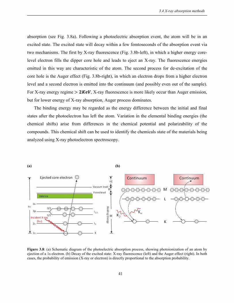
41
absorption (see Fig. 3.8a). Following a photoelectric absorption event, the atom will be in an
excited state. The excited state will decay within a few femtoseconds of the absorption event via
two mechanisms. The first by X-ray fluorescence (Fig. 3.8b-left), in which a higher energy core-
level electron fills the dipper core hole and leads to eject an X-ray. The fluorescence energies
emitted in this way are characteristic of the atom. The second process for de-excitation of the
core hole is the Auger effect (Fig. 3.8b-right), in which an electron drops from a higher electron
level and a second electron is emitted into the continuum (and possibly even out of the sample).
For X-ray energy regime , X-ray fluorescence is more likely occur than Auger emission,
but for lower energy of X-ray absorption, Auger process dominates.
The binding energy may be regarded as the energy difference between the initial and final
states after the photoelectron has left the atom. Variation in the elemental binding energies (the
chemical shifts) arise from differences in the chemical potential and polarizability of the
compounds. This chemical shift can be used to identify the chemicals state of the materials being
analyzed using X-ray photoelectron spectroscopy.
(a)
(b)
Figure 3.8: (a) Schematic diagram of the photoelectric absorption process, showing photoionization of an atom by
ejection of a 1s electron. (b) Decay of the excited state: X-ray fluorescence (left) and the Auger effect (right). In both
cases, the probability of emission (X-ray or electron) is directly proportional to the absorption probability.
3.4 X-ray absorption methods

42
3.4.1 X-ray Photoelectron Spectroscopy (XPS)
Surface analysis by XPS is accomplished by irradiation a sample with mono-energetic X-rays
(1253.6 eV) or (1486.6 eV), as usual. Theses photons have limited penetrating
power in a solid on the order of 1-10 micrometers. They interact with the atoms in the surface
region; causing electrons to be emitted by the photoelectron effect (see Fig. 3.9a). While
ionization occurs to a depth of a few micrometers, only those electrons that originate within tens
of angstroms below the solid surface can leave the surface without energy loss. These electrons
produce the peaks in the spectra and the electrons that undergo inelastic loss processes before
emerging form the background. The intensity of electron ( ) emitted from all depths greater than
in a direction normal to the surface is given by the Beer-Lambert relationship [71]:
(3.43)
were is the initial intensity, is analysis depth, is attenuation depth and is angle of
emission measured with respect to the surface normal. A appropriate analysis of the above
equation shows that for , some 65% of the signal in electron spectroscopy will originate
from depth of less than 1λ, 85% from a depth of , and 95% from a depth of , as
illustrated in Fig. 3.9b. The values of the attenuation depth is of the order of a few nanometres,
thus the depth from which information can be derived is a few nanometers. The Beer-Lambert
equation can be manipulated in a variety of ways to provide information about over-layer
thickness and to provide a non-destructive depth profile.
3.4 X-ray absorption methods
3 Surface and interface characterization methods

43
(a)
(b)
Figure 3.9: (a) Schematic of X-ray photoelectron spectroscopy, the horizontal dashed line indicates a distance from
the surface of the attenuation length, λ. (b) The variation of electron intensity with analysis depth.
The depth of analysis in electron spectroscopy
The depth of analysis in XPS varies with the kinetic energy of the electron under consideration. It
is determined by a quantity known as the attenuation length (λ) of electrons, which is related to
the inelastic mean free path length (IMFP). In general, the attenuation length is about 10 percent
less than the IMFP. A relationships which relate λ to electron energy and material properties was
proposed by Seah and Dench [72] as:
(3.44)
where is the energy of the electron in , is the volume of the atom in
and is in .
The calculated attenuation length of electrons vs. electron energy for Silicon is illustrated in Fig.
3.10a showing an increasing attenuation length of electron with electron energy for energy of
above 50 eV.
3 Surface and interface characterization methods

44
Non-destructive depth profiling methods
XPS can provide compositional information as a function of depth. This can be achieved by
manipulating the Beer-Lambert equation either to increase or to decrease the integral depth of
analysis non-destructively by changing the geometry of the experiment. As the depth of analysis
depends on the angle of emission via (see Eq. 3.43), at high value of a spectrum is
recorded with extremely surface sensitivity. As normal electron emission is approached ( ),
the analysis depth move towards the limiting value of ~ 3λ. The variation of sampling depths at
different emission angles are illustrated schematically in Fig. 3.10b.
An alternative method for depth profiling is the variation of analysis depth via tuning energy
of the emitted electron. This method can be carried out using synchrotron radiation providing
variable X-ray photon energies. The variation of attenuation depth with kinetic energy, giving a
possibility to obtain a degree of depth selectivity, is shown in Fig. 3.10c.
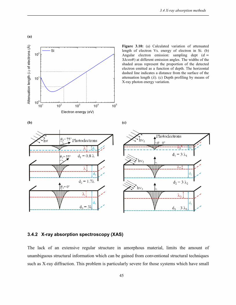
45
(a)
Figure 3.10: (a) Calculated variation of attenuated
length of electron Vs. energy of electron in Si. (b)
Angular electron emission: sampling dept ( ) at different emission angles. The widths of the
shaded areas represent the proportion of the detected
electron emitted as a function of depth. The horizontal
dashed line indicates a distance from the surface of the
attenuation length ( ). (c) Depth profiling by means of
X-ray photon energy variation.
(b)
(c)
3.4.2 X-ray absorption spectroscopy (XAS)
The lack of an extensive regular structure in amorphous material, limits the amount of
unambiguous structural information which can be gained from conventional structural techniques
such as X-ray diffraction. This problem is particularly severe for those systems which have small
3.4 X-ray absorption methods

46
percentages of impurity atoms. XAS is a technique which can probe the structure of atoms
surrounding each species of atom in the material simply by tuning the X-ray energy to the
absorption edge of that element [73]. Importantly, crystallinity is not required for XAS
measurements, making it one of the few structural probes available for non-crystalline and highly
disordered materials. The X-ray absorption spectrum is typically divided into two regimes: X-ray
absorption near edge spectroscopy (XANES) and extended X-ray absorption fine-structure
spectroscopy (EXAFS). XANES is strongly sensitive to formal oxidation state and coordination
chemistry of the absorbing atom, while the EXAFS is used to determine the distance, coordinate
number, and species of neighbours of the absorbing atom.
EXAFS and near-edge structure
The photoelectric absorption process leads to a sharp rise in the absorption intensity. This sharp
rise is denoted as absorption edge (E0). For EXAFS, we are concerned with the intensity of as a
function of energy, near and at energies just above the of a known core level of a known
atomic species defined by [74]:
(3.45)
EXAFS can be measured either in transmission or fluorescence geometries. The energy
dependence of the absorption coefficient is measured either in transmission as
(3.46)
Or in X-ray fluorescence as
(3.47)
where, is the monitored intensity of a fluorescence line associated with the absorption process.
EXAFS is best understood in terms of the wave behaviour of the photon-electron created in the
absorption process. It is common to convert the X-ray energy to , the wavevector of the
photoelectron,
3 Surface and interface characterization methods

47
√
(3.48)
with the wavevector, the electron mass and Plank’s constant ( . The primary
quantity for EXAFS is then , the oscillation as a function of photoelectron wave vector and
decay quickly with . To emphasize the oscillations, is often multiplied by a power of
typically or .
The different frequency apparent in the oscillations in corresponded to different near-
neighbor coordination shells which can be described and modelled according to the EXAFS
equation.
Theoretical outline
EXAFS is best understood in terms of the wave behaviour of the photoelectron created in the
absorption process. Quantum mechanically the outgoing photoelectron can be represent as a
spherical wave with wavelength define as , (Fig. 3.11a) that scatters at
neighbouring atoms (e.g., electron density), producing a backscattered wave (Fig. 3.11b). The
outgoing and backscattered waves interfere, causing an interference pattern varying between total
construction and total destruction. Since the path lengths of both waves define their final phases,
it can be seen that the distance to the neighbouring atoms determine the interference pattern. The
absorption coefficient exhibits a fine structure because the final wave state function is modulated
due to the interference pattern.
Fig. 3.11c shows a photoelectric effect, in which an X-ray is absorbed by a core-level with
BE, and a photoelectron with wave number is created and propagates away from the atom.
When a neighbouring atom is included in the Fig. 3.11d, the photoelectron can scatter from the
electrons of this neighbouring atom, and the scattered photo-electron can return to the absorbing
atom. Since the absorption coefficient depends on whether there is an available electronic state
(that is whether there is an electron at the location of the atom and at the appropriate energy and
momentum), the presence of the photoelectron scattered back from the neighbouring atom will
alter the absorption coefficient. This is the origin of XAFS.
3.4 X-ray absorption methods
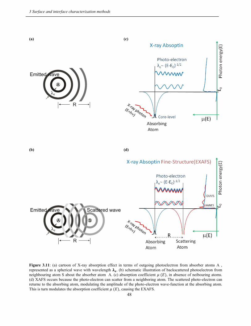
48
(a)
(c)
(b)
(d)
Figure 3.11: (a) cartoon of X-ray absorption effect in terms of outgoing photoelectron from absorber atoms A ,
represented as a spherical wave with wavelength . (b) schematic illustration of backscattered photoelectron from
neighbouring atom S about the absorber atom A. (c) absorption coefficient , in absence of neibouring atoms.
(d) XAFS occurs because the photo-electron can scatter from a neighboring atom. The scattered photo-electron can
returne to the absorbing atom, modulating the amplitude of the photo-electron wave-function at the absorbing atom.
This is turn modulates the absorption coefficient , causing the EXAFS.
3 Surface and interface characterization methods
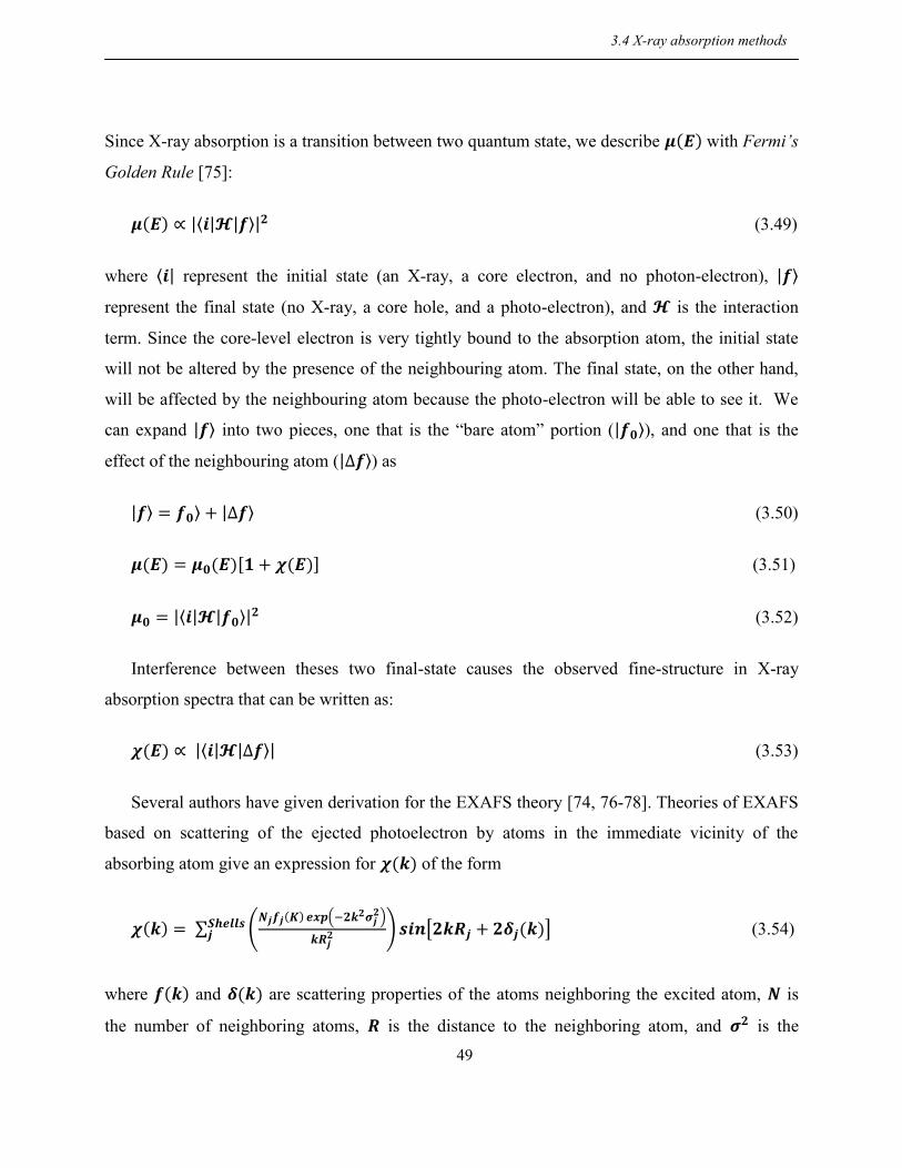
49
Since X-ray absorption is a transition between two quantum state, we describe with Fermi’s
Golden Rule [75]:
|⟨ | | ⟩| (3.49)
where ⟨ | represent the initial state (an X-ray, a core electron, and no photon-electron), | ⟩
represent the final state (no X-ray, a core hole, and a photo-electron), and is the interaction
term. Since the core-level electron is very tightly bound to the absorption atom, the initial state
will not be altered by the presence of the neighbouring atom. The final state, on the other hand,
will be affected by the neighbouring atom because the photo-electron will be able to see it. We
can expand | ⟩ into two pieces, one that is the “bare atom” portion (| ⟩), and one that is the
effect of the neighbouring atom (| ⟩) as
| ⟩ ⟩ | ⟩ (3.50)
(3.51)
|⟨ | | ⟩| (3.52)
Interference between theses two final-state causes the observed fine-structure in X-ray
absorption spectra that can be written as:
|⟨ | | ⟩| (3.53)
Several authors have given derivation for the EXAFS theory [74, 76-78]. Theories of EXAFS
based on scattering of the ejected photoelectron by atoms in the immediate vicinity of the
absorbing atom give an expression for of the form
∑ ( (
)
)
[ ] (3.54)
where and are scattering properties of the atoms neighboring the excited atom, is
the number of neighboring atoms, is the distance to the neighboring atom, and is the
3.4 X-ray absorption methods

50
disorder in the neighbour distance. The EXAFS equation allows us to determine , , and
knowing the scattering amplitude and phase-shift . Furthermore, since theses scattering
factors depend on the Z of the neighbouring atom, EXAFS is also sensitive to the atomic species
of the neighbouring atom [79, 80].
3 Surface and interface characterization methods

51
3.5 Experimental procedure
Synchrotron radiation sources
In a conventional tube, X-ray are generated if energetic electrons are stopped by impact with a
metal target. The brightness of X-ray in this process is limited by thermal properties of solids.
When electrons are confined to a circular orbit in a storage ring by a magnetic field,
electromagnetic radiation is emitted due to the acceleration towards the center of the circle. At
relativistic velocities, the emission becom strong in the forward direction and tangentional to the
electron orbit. In a storage ring designed for production of synchrotron radiation, the orbit is not
circular but consists of dipole bending magnets separated by straight sections. Beamlines are
constructed to extract the beam from tangent points of the bending magnets or from insertion
devices within the straight sections. In the latter, the electron beam is deflected in a small radius
of curvature by a succession of dipole magnets of alternating sense: wigglers, in which the
amplitude of oscillation is larger with respect to that of emitted radiation, and undulator in which
it is small. General properties on synchrotron facilities are introduced in [81].
Figure 3.12: Schematic diagram of an electron storage ring and optics of synchrotron radiation: X-rays are created in
the synchrotron storage ring and extracted into beamline. A Si (111) monochromator is used to select a certain
wavelength out of the spectrum of source and mirrors guide and focus the beam further to the sample position. The
energy of the beam is changed by changing the angle between the monochromator craytal and the incident beam.
3.5 Experimental procedure

52
Fig. 3.12 depicts schematically an experimental setup of measurements. Synchrotron radiation
from the storage ring is monochromatized with either double crystal or a curved mirror
monochromator.
Experimental setup
Most of the experiments at this work were done using synchrotron radiation at:
DELTA (1.5 GeV synchrotron radiation facility at TU-Dortmund)
Surface sensitive GI-XAS experiments were performed at beamline BL8 [82] at the
superconducting asymmetric wiggler at DELTA [83] in the fluorescence mode. The emitted
fluorescence radiation was recorded by a Si pin-diode detector placed at 90° with respect to the
incident beam. For the XAS measurements, the excitation energy was varied in steps of 0.5 eV
from -50 to 1000 eV across the Fe K-edge located at 7.112 keV using a Si(111) double crystal
monochromator. The incident beam intensity was monitored by a N2-gas filled ionization
chamber, and the fluorescence data were recorded using a multi-channel analyzer and a digital
processor. The energy scale of the monochromator was calibrated simultaneously for each sample
by measuring an iron foil which was equipped between the second and a third ionization chamber
in transmission mode. Due to the grazing incidence condition, the footprint of the incident beam
with size of 50 m 5 mm (vertical horizontal) was about 8 mm along the beam pass,
matching the whole length of the samples. The experimental setup is shown in Fig. 3.13a. The
measured absorption spectra have been analyzed with the software ATHENA which is included
in the IFEFFIT program package for X-ray absorption spectroscopy analysis [84]. This includes
normalization of all spectra and calibration with respect to the Fe K-edge.
The XPS experiments were carried out at the soft X-ray undulator beamline BL-11 of the
DELTA storage ring [85] using a hemispherical electron energy analyzer. A variation of the
excitation energies were used for compositional depth profiling. The Si 2p and Fe 3p core levels
as well as the valence band (VB) distributions were used to evaluate the formed silicides in
different stoichiometries using the energy of the C 1s peak (284.8 eV) as reference for the
3.6 Experimental procedure
3 Surface and interface characterization methods

53
binding energy (BE) scale. Each spectrum was fitted by a Shirley type background and Gaussian
peak functions using the Fityk software [86]. Experimental setup is shown in Fig. 3.13b.
Figure 3.13: (a) The setup for a fluorescence grazing
incidence X-ray absorption spectroscopy (GI-XAS)
experiment at BL8 at DELTA. The incident beam intensity
( and the reflected beam intensity ( are measured by the
ionization chambers. The emitted fluorescence radiation (
was recorded by a Si pin-diode detector placed at 90° with
respect to the incident beam. (b) A picture of the whole
experimental X-ray photoelectron spectroscopy (XPS) setup
at beamline 11 at DELTA.
3.5 Experimental procedure

54
ANKA (Synchrotron radiation facility at Karlsruhe institute of technology)
Surface sensitive EAD experiments with tuning wavelength were performed at beamline PDIFF
at ANKA using 4-circle geometry Kappa-diffractometer equipped with Vantec-1 PSD Detector.
The beam from 1.5T bending magnet source focuses on sample position using horizontally &
vertically focusing mirror system (cut-off energy 21 keV). Depth profiling was carried out by
energy tuning from 8500 eV to 8900 eV using a Si(111) double crystal monochromator. A sketch
of the experimental set up is shown in Fig. 3.14
Figure 3.14: Experimental setup at BL-PDIF at ANKA: The 4-circle Kappa-goniometer equipped with a Vantec-1
PSD behind an evacuated tube. The photon energy was changed in the range of 8750 and 8900 eV to achieve Si(311)
reflection in coplanar extremely asymmetry geometry. The incidence and diffracted beam direction were shown by
yellow arrows. The sample state so that the surface normal [001] be perpendicular to incoming beam direction.
3 Surface and interface characterization methods
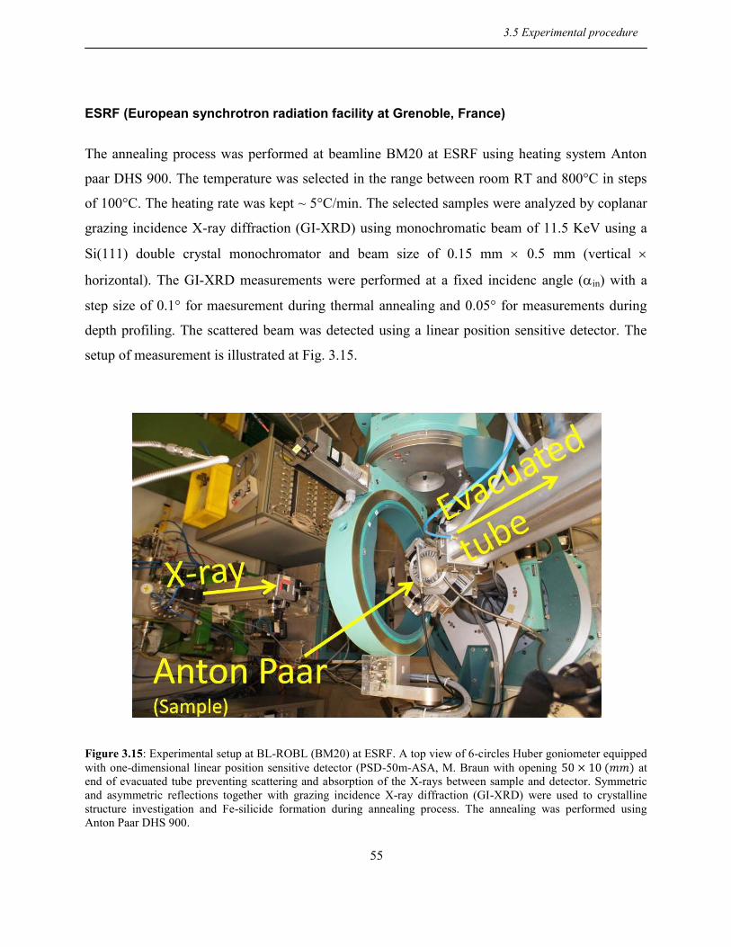
55
ESRF (European synchrotron radiation facility at Grenoble, France)
The annealing process was performed at beamline BM20 at ESRF using heating system Anton
paar DHS 900. The temperature was selected in the range between room RT and 800°C in steps
of 100°C. The heating rate was kept ~ 5°C/min. The selected samples were analyzed by coplanar
grazing incidence X-ray diffraction (GI-XRD) using monochromatic beam of 11.5 KeV using a
Si(111) double crystal monochromator and beam size of 0.15 mm 0.5 mm (vertical
horizontal). The GI-XRD measurements were performed at a fixed incidenc angle (in) with a
step size of 0.1° for maesurement during thermal annealing and 0.05° for measurements during
depth profiling. The scattered beam was detected using a linear position sensitive detector. The
setup of measurement is illustrated at Fig. 3.15.
Figure 3.15: Experimental setup at BL-ROBL (BM20) at ESRF. A top view of 6-circles Huber goniometer equipped
with one-dimensional linear position sensitive detector (PSD-50m-ASA, M. Braun with opening at
end of evacuated tube preventing scattering and absorption of the X-rays between sample and detector. Symmetric
and asymmetric reflections together with grazing incidence X-ray diffraction (GI-XRD) were used to crystalline
structure investigation and Fe-silicide formation during annealing process. The annealing was performed using
Anton Paar DHS 900.
3.5 Experimental procedure

56
Home-lab setup
The XRR measurements have been performed with a high-resolution diffractometer GE HR-
XRD 3003 with radiation by laboratory setup. Some of XRR was measured using a 2D
focussing Goebel mirror and sufficient small detector slits. The experimental XRR curves were
simulated using the software RC_REF_SIM_win [17] which is based on the dynamical theory of
X-ray reflection using the matrix approach [18] and roughness is considered following the Névot-
Croce algorithm [19].
To achieve higher sensitivity and to evaluate the effect of implantation on the density of the
damaged surface region, EAD in non-coplanar geometry was applied using the same instrument.
A Bartels type monochromator was used to obtain radiation.
Figure 3.16: Experimental setup at hom-lab. A high-resolution diffractometer (GE HR-XRD 3003) with
radiation and a 4-circle goniometer equipped with a PSD, analyzer and monochromator was used for X-ray
reflectivity measurement and Si(331) reflection at extremely asymmetry non-coplanar geometry.
3 Surface and interface characterization methods
57
The measurements have been performed using a beam size of 1.5 1.5 mm² and an open detector
without the use of an analyzer crystal. Rocking curves (RCs) of the Si (331) reflection were
recorded at different fixed incidence angles in the range from 0° up to 1° using the HKL mode of
SPEC [20]. For data evaluation, RCs of the Si (331) reflection were calculated using the GID-Sl
code from Sergey Stepanov X-ray server base on dynamical diffraction theory
(http://sergey.gmca.aps.anl.gov/). The setup of measurement is illustrated at Fig. 3.16.
The surface morphologies were analyzed ex-situ using a multimode atomic force microscope
(Veeco) in tapping mode at HZDR and a Dimension 3000 system with Nanoscope IIIa controller
from VEECO (former DIGITAL INSTRUMENTS) operating in Tapping Mode at IOM-leipzig.
The AFM images presented in this report have a resolution of 512 × 512 pixels or higher and
were performed using Si probes with (nominal) tip radii smaller than 7 nm. The roughness is
extracted from the spatial height distribution. For the AFM processing WSxM was used [87].
In order to analyze locally the microstructure and the surface morphology of the Fe-irradiated
Si samples as function of depth, cross-sectional transmission electron microscopy (TEM)
investigations were performed using an image-corrected Titan 80-300 microscope (FEI) in
HZDR. Employing a Gatan Imaging Filter 863, energy-filtered TEM (EFTEM) was used to study
the chemical composition of the near-surface region of the samples. In particular, the Three-
Window-Method was applied to extract the Fe and Si distributions. Classical cross-sectional
TEM specimens were prepared by sawing, grinding, dimpling, and final Ar ion milling. Prior to
each TEM analysis, the specimen mounted at a double tilt analytical holder was placed into a
Model 1020 Plasma Cleaner (Fischione) for 45 s to remove organic contamination.
In addition, some of samples have been investigated by Rutherford backscattering
spectrometry (RBS) and secondary ion mass spectrometry (SIMS) in HZDR and IOM-Leipzig. In
particular, depth profiles of the atomic composition were obtained using dual beam time-of-flight
secondary ion mass spectrometry (TOF-SIMS). 0.5 keV O2+ was used for erosion and
15 keV Ga+ for analysis. The analysis area was 40 × 40 µm
2. According to the etching times and
the final depths of the etched regions (determined by white light interferometry) depth profiles
were obtained. The RBS measurements were performed at the nanoprobe LIPSION (the ion beam
facility of the University of Leipzig) with a 2.0 MeV He+ beam. The backscattered ions were
3.5 Experimental procedure

58
detected at an angle of 170° with a CANBERRA Annular (passivated implanted planar silicon)
PIPS detector. For the data analysis the RUMP-code was applied [88].
3 Surface and interface characterization methods

59
4 Pattern formation on direct off-normal Fe ion irradiated Si(100)
surfaces
In this chapter, we report on nanopattering on Si(100) surfaces under an off-normal irradiation
process with energetic Fe ions. Depth resolved investigations using nondestructive X-ray methods
were carried out to find out the effective parameters influencing the pattern formation
mechanism. In section 4.1, the experimental parameters of the prepared sample are given. In
section 4.2, the morphologies of the surfaces and interfaces under different irradiation parameters
(ion energy and ion fluence), revealed by atomic force microscopy (AFM) and transition electron
microscopy (TEM), are reported. In section 4.3, the ion beam induced variations in surface
density using X-ray reflectivity (XRR) and extremely asymmetric diffraction (EAD) methods are
represented.
4.1 Sample preparation
For this work, series of the samples have been prepared using the Danfysik 1050 low energy ion
implanter at Helmholtz-Zentrum Dresden-Rossendorf. Two sides polished Si(100) wafers
(nominally without miscut) with a size of (10 10 mm2) and thickness of 500 μm were irradiated
homogeneously with a scanned Fe+ beam of 5 mm diameter. The irradiation parameters are
summarized in table 4.1.
Table. 4.1 The parameters of ion energy, , ion fluence, , ion incidence angle, , at Fe ion irradiation
process on Si(100) surfaces.
Samples (KeV) Samples (KeV) (ions cm-2
) (°)
1A 5 1B 20 11016
65
2A 5 2B 20 51016
65
3A 5 3B 20 11017
65
4A 5 4B 20 51017
65

60
4.2 Surface and interface morphology analysis
AFM analysis
The AFM analysis demonstrates the formation of variety of topographies on Si surfaces under Fe
ion irradiation process. Figs. 4.1(a-d) show the AFM images of oblique bombarded Si surfaces
with 5 KeV Fe ions (series A samples) with fluence of 11016
ions cm-2
(sample 1A), 51016
ions
cm-2
(sample 2A), 11017
ions cm-2
(sample 3A), and 51017
ions cm-2
(sample 4A), respectively.
While the surface remains smooth for the lower fluence (1A), the morphologies of the other
samples changes from oriented chains (2A) over irregularly oriented ripples (3A) to short-
distance ripples (4A). The extracted height histograms from AFM images of patterned samples
are illustrated in Fig 4.1e from left to right hand side corresponding to samples 2A, 3A and 4A,
respectively. The average height increases from 0.64 nm for the sample 1A to 4.41, 7.12 and
21.09 nm for the samples 2A, 3A, and 4A, respectively (Fig. 4.1e). For the height variation
analysis of the resulted surface topographies, a statistically root mean square (RMS) parameter
can be calculated from the height profiles from the AFM images by [89]:
⟨ ⟩ {
∑ ⟨ ⟩
}
(4.1)
where ⟨ ⟩ is the average surface height, and N is the number of measured points.
It can be assumed that there is a correlation between the RMS roughness and the amplitude of
the topographical features in surface topography with one dimensional length scale. The extracted
RMS roughnesses from the AFM images are calculated to be σ1A = 0.2 nm, σ2A = 0.98 nm, σ3A =
2.4 nm and σ4A = 4.65 nm for the sample 1A, 2A, 3A, and 4A, respectively.
4 Pattern formation on direct off-normal Fe ion irradiated Si(100) surfaceswerden soll.

61
Figure 4.1: AFM images of Si surfaces irradiated with 5 keV Fe ions at 65° incidence angle with respect to the
surface normal at different fluencies: (a) Sample 1A (zmax = 5.09 nm, = 0.2 nm) at 1 1016
ions cm-2
. (b)
Sample 2A (zmax = 14.65 nm, = 0.98 nm) at 5 1016
ions cm-2
. (c) Sample 3A (zmax = 17.7 nm, = 2.4 nm)
at 1 1017
ions cm-2
. (d) Sample 4A (zmax = 41.39 nm, = 4.65 nm) at 5 1017
ions cm-2
. The z is the height
difference corresponding to the colour scale range. The images size is 3 × 3 µm2. (e) Corresponding height
histograms extracted from AFM images, ordered from left to right hand side for the samples 2A, 3A, and 4A.
86420
2e4
1.5e4
1e4
5e3
0
Height (nm)
Nu
mb
er o
f ev
ents
(a.
u.)
151050
6e3
5e3
4e3
3e3
2e3
1e3
0
Height (nm)
Nu
mb
er o
f ev
ents
(a.
u.)
3020100
7e3
6e3
5e3
4e3
3e3
2e3
1e3
0
Height (nm)
Nu
mb
er o
f ev
ents
(a.
u.)
(a) (b)
(c) (d)
(e)
4.2 Surface and interface morphology analysis

62
The surface morphologies of the series B samples bombarded with 20 KeV Fe ions with fluences
similar as series A samples are shown in Figs. 4.2(a-d). While for sample 1B the surface remains
smooth, increasing the ion fluence for other samples causes modulation of surface morphologies
in different way as shown in samples A, so that the surface morphologies change from random
ripple like for the sample 2B over short range oriented ripples for the sample 3B to columnar like
oriented nanodots for the sample 4B. The extracted RMS roughnesses from height profile of
AFM images are σ1B = 0.2 nm for the sample 1B, σ2B = 2.3 nm for the sample 2B, σ3B = 7.39 nm
for the sample 3B, and σ4B = 17.28 nm for the sample 4b.
Figure 4.2: AFM images of Si surfaces irradiated with 20 keV Fe ions at 65° incident angle with respect to the
surface normal at different fluencies: (a) Sample 1B (zmax = 2.5 nm, = 0.2 nm) at 1 1016
ions cm-2
. (b)
Sample 2B (zmax = 17.35 nm, = 2.3 nm) at 5 1016
ions cm-2
. (c) Sample 3B (zmax = 53.52 nm, = 7.39
nm) at 1 1017
ions cm-2
. (d) Sample 4B (zmax = 131.4 nm, = 17.28 nm) at 5 1017
ions cm-2
. The z is the
height difference corresponding to the colour scale range. The imagines size is 3 × 3 µm2.
(a) (b)
(d) (c)
4 Pattern formation on direct off-normal Fe ion irradiated Si(100) surfaceswerden soll.

63
Fig. 4.3a shows the comparison between extracted RMS roughness as a function of ion fluence
for the samples A (blue curve) and B (red curve). While for both series of the samples an onset of
ion fluence for pattern formation is above the 1 1016
ions cm-2
, by increasing ion fluence the
pattern amplitude increases exponentially for both series of the samples till ion fluence of 1
1017
ions cm-2
and after that the amplitude increases linearly with trend to saturation at higher ion
fluences. This saturation can be attributed to dominant nonlinear effects at higher ion fluence and
can not be predicted by BH model (see subsection 2.3). Furthermore, for the higher ion energy
the pattern amplitude becomes larger at all ion fluences.
Fig. 4.3b shows the variation of average height with ion energy for ion fluences of 5 1016
ions cm-2
(black triangle line), 1 1017
ions cm-2
(red circle line), and 5 1017
ions cm-2
(blue
rectangular line). It can be seen that the variation of the average height of the patterns at higher
ion fluence strongly depends on ion energy. Therefore, the surface patterning process depends on
ion fluence and ion energy as well.
(a)
(b)
Figure 4.3: Root mean square (RMS) roughness as a function of ion fluence for the samples series A (blue) and
series B (red). (b) Fluctuation of average height with ion energy at ion fluence 5 1016
ions cm-2
(black triangle
line), 1 1017
ions cm-2
(red circle line), and 5 1017
ions cm-2
(blue square line).
4.2 Surface and interface morphology analysis

64
As the RMS roughness is a first order statistical quantity which only reflects the properties of the
individual points which give no information on lateral dimension of the patterns. For this, the
second order statistical quantity as called the power spectral density (PSD), is used to characterize
the relationship of two points or frequency properties of the topography on the surface. The PSD
function is obtained by performing two Dimensional Fast Fourier Transform (2D-FFt) of the
height profile from the AFM image. For instance, the FFT diagram corresponding to AFM image
of sample 2B is illustrated in Fig 4.4a. The appeared rings indicate the existence of periodic
component in the topography. From the position of first lighter rings at FFT image, characteristic
frequency of periodic elements (the inverse of the separation of the features in the real space) can
be obtained. The separation will be considered to be wavelength in the case of ripple and the
mean size in the case of dots pattern. The width of the spots is related to the homogeneity and
spatial correlation of features. To facilitate the quantification of the information presented in the
FFT diagram, the calculated PSD function from the FFT image is shown in Fig. 4.4b. The
position of the peak indicates the characteristic spatial frequency of the ripples in the real space
(1/wavelength of the ripples) and provides quantitative information about height and lateral
distributions.
Fig. 4.4c shows the calculated wavelength of surface pattern as a function of ion fluence for
the series A (red) and B (blue) samples. It can be seen that the wavelength increases from 83 nm
to 195 nm for the samples A and from 45 nm to 65 nm for the samples B when ion fluence
increases from 5 1016
ions cm-2
to 5 1017
ions cm-2
.
Fig. 4.4d shows the variation of pattern wavelength versus ion energy for ion fluences of 5
1016
ions cm-2
(black triangle line), 1 1017
ions cm-2
(red circle line), and 5 1017
ions cm-2
(blue
rectangular line). It seen that variation of pattern wavelength is more pronounced at 20 KeV ion
energy compared to 5 KeV. The dependence of the lateral size of the ripples and dots pattern on
ion energy and fluence represents a capability of pattern size controlling by means these ion
parameters.
4 Pattern formation on direct off-normal Fe ion irradiated Si(100) surfaceswerden soll.

65
(a)
(b)
(c)
(d)
Figure 4.4 (a) Fast fourier transform (FFT) image corresponding to the sample 2B. (b) Power spectral density (PSD)
diagram corresponded to FFT image of sample 2B. K is spetial frequency. (c) The variation of wavelength with ion
fluence for ion energy of 5 KeV (samples series A-red) and 20 KeV KeV (samples series B-blue). (d) The variation
of wavelength with ion energy at fluence of 5 1016
ions cm-2
(black), 1 1017
ions cm-2
(red), and 5 1017
ions cm-2
(blue).
-1-1.5-2-2.5-3-3.5
4
3
2
1
-0
-1
-2
log(k[{1/nm}])
log
(PS
D[n
m4])
4.2 Surface and interface morphology analysis

66
TEM analysis
TEM analysis was applied to investigation of interface morphologies and evaluation of cross
section of pattern geometries. Fig. 4.5 shows TEM images intersection of the sample series A
ordering from top to down as increasing ion fluence from sample 1A to 4A, respectively. It can
be seen while the surface remains smooth for the sample 1A irradiated with lower ion fluence,
ripples form on surface for increasing ion fluence accompanied by increasing ripple wavelength,
as shown by dashed vertical lines, from 45 nm for the sample 2A to 65 nm for the sample 4A
over 55 nm for the sample 3A. It can be seen that the wavelength and amplitude of the ripples
increase by increasing the ion fluence as were shown from AFM analysis.
Figure 4.5: The cross-sectional TEM images of the Si
surfaces after irradiation with 5 keV Fe ions at incidence
angle of 65° with respect to the surface normal with a
fluence of 1 1016
ions cm-2
(sample 1A), 5 1016
ions
cm-2
(sample 2A), 1 1017
ions cm-2
(sample 3A), and 5
1017
ions cm-2
(sample 4A), from top to down,
respectively. The dashed vertical lines show the
variation of ripple wavelength with ion fluences. The
blue array shows the direction of incoming Fe ions.
4 Pattern formation on direct off-normal Fe ion irradiated Si(100) surfaces
werden soll.

67
Fig. 4.6a shows a zero-loss filtered image of sample 1A. Directly below the glue, which is used
for TEM sample preparation, an approximately 2 nm thick Si oxide surface layer (marked by two
white dashed lines) is visible followed by a dark layer of 2 nm thickness which is marked by two
dashed yellow lines. This is an Fe-rich film as confirmed by the Fe elemental map shown in Fig.
4.6b. Below this Fe-rich layer, the Fe concentration is decreasing towards the bulk. The structure
of this 5 nm thick layer is still amorphous. Fig. 4.6c shows the Si element map of the sample 1A
from same field of view as Fig. 4.6a. It can be seen that for low ion fluence the Si surface remains
flat.
Figure 4.6: (a) The cross-sectional
zero-loss filtered TEM images of the
Si surface after irradiation with 5 keV
Fe ions at incidence angle of 65° with
respect to the surface normal with a
fluence of 1 1016
ions cm-2
(sample
1A). Corresponding element map of
(b) Fe and (c) Si from the same field
of view. The inset shows the obtained
depth density profile from X-ray
reflectivity (see Fig. 4.8b).
(a)
(b)
(c)
4.2 Surface and interface morphology analysis

68
Fig. 4.7a shows the cross-sectional zero-loss filtered image of sample 4A confirming the
formation of ripples with an amplitude of ~ 10 nm on the Si(100) surface. Covered by glue from
TEM sample preparation, the layer with bright contrast, which is marked by two white lines in
Fig. 4.7a, corresponds to amorphous Si oxide. The dark ellipsoidal shaped areas at the front
slopes of the ripples can be attributed to Fe-rich amorphous Fe-Si which is accompanied by few
nanometer amorphous buried areas with decreasing Fe concentration towards the crystalline bulk
Si (Figs. 4.7b-c). Derived from Fig. 4.7a, the ripple cross section shows an asymmetrical triangle
with side angles of about 32° and 10° at the front slope, facing the incoming beam, and at the rear
slope, respectively.
Figure 4.7: (a) The cross-sectional
zero-loss filtered TEM images of the Si
surface after irradiation with 5 keV Fe
ions at incidence angle of 65° with
respect to the surface normal with a
fluence of 5 1017
ions cm-2
(sample
4A). Corresponding element map of (b)
Fe and (c) Si from the same field of
view.
(a)
(b)
(c)
4 Pattern formation on direct off-normal Fe ion irradiated Si(100) surfaceswerden soll.

69
The ion incident angle with respect to normal of the flat surface (n2 in Fig 4.7a) is = 65°.
From the ripple geometry, the local ion incidence angles with respect to the the normal of the
front slope (n1 in Fig. 4.7a) and rear slope (n3 in Fig. 4.7a) are = - 32° =33° and =
+ 10° = 75°, respectively. The ion beam hitting the local surface at the front slope under 33° will
penetrate deeper in the bulk than ions hitting the rear slope under 75°. Consequently, the Fe
concentration is much higher at the thicker front slope compared to the thinner rear slope. By
increasing the ion fluence, Fe atoms are accumulated in the crest of the ripples.
4.3 Depth density profiling of Si(100) after irradiation with Fe ions
4.3.1 X-ray reflectivity
The density profiles perpendicular to Fe ions irradiated Si surfaces were investigated using XRR.
Fig. 4.8a shows the measured XRR curves of the samples 1A (black curve), 2A (red curve), 3A
(blue curve), 4A (olive curve), and the non-irradiated Si (gray curve). For angles =
0.23° (critical angle of Si at radiation), the reflectivity of the sample 1A decreases with
oscillations superimposed indicating a layering close to the surface. This layering is still visible
for sample 2A but hard to see for the samples 3A and 4A. The mean density profile of the sample
1A in the direction of the surface normal was analyzed quantitatively by XRR. Fig. 4.8b shows
the simulation of XRR curve of the sample 1A providing the relative density profile as a function
of depth. To this end, the near surface region was divided into a number of thin lamellae with
constant electron density. Both thickness and density of each lamella were varied until a
coincidence between measured and simulated curves was reached.
The inset of Fig. 4.8b shows the fitted mean density profile as a function of depth. Close to
the surface the mean density is found to be increased with respect to the non-irradiated silicon
(2.33 g/cm³), showing the incorporation of Fe ions close to the surface. The density reaches its
maximum in a depth of 2 nm below the surface, while the total thickness of the layer with
enhanced Fe atoms reaches 6 nm. The mean density of the irradiated region amounts to about 2.7
g/cm³. The evaluated density profile is in qualitative agreement with TRIDYN calculations [90].
For an irradiation fluence that is larger than 1 1016
ions cm-2
, TRIDYN reveals a 3 nm sub-
surface layer with an Fe concentration of 10 at % followed by a slow drop reaching zero value at
4.3 Depth density profiling of Si(100) after irradiation with Fe ions
70
a depth of 10 nm. TRIDYN shows that above a certain fluence ( > 51015
ions/cm2) the Fe
concentration saturates and is reaching a stable value. The onset of pattern formation should be
above this threshold. However, TRIDYN does not take into account a surface roughening or
pattering, while only the sputtering effect itself is taken into account. Note that this small ion
penetration depth of a few nanometres only is comparable to the amplitude of surface
corrugations induced by the ion beam processes at larger fluences found for samples 2-4A.
Fig. 4.8c shows the measured XRR curves of samples 1B (black curve), 2B (red curve), 3B
(blue curve), 4B (olive curve), and the non-irradiated Si (gray curve). The reflectivity of sample
1B contains oscillations with less number and lower amplitude compared to the sample 1A
consequently thinner layering close to surface with less density variation. Fig. 4.8d shows the
simulated XRR curve of sample 1B providing the relative density profile as a function of depth.
The inset of Fig. 4.8d shows the fitted density profile as a function of depth. The density reaches
its maximum in a depth of 1 nm below the surface, while the total thickness of the layer with
enhanced Fe atoms reaches 4 nm. The mean density of the irradiated region is calculated amounts
to about 2.36 g/cm³ that is in the range of the non-irradiated Si. An obtained smaller mean density
for sample 1B compared to sample 1A can be attributed to the larger sputtering yield at sample
1B compared to sample 1A. The calculated sputtering yield using SRIM 2008 (www.SRIM.org)
shows that the sputtering yield increases from 9.2 at 5 KeV ion energy (sample 1A) to 13.54 at 20
KeV ion energy (sample 1B). This 48% increasing at total sputtering yield can be related to
smaller mean density at sample 1B.
For the XRR experiment, the larger surface roughness of the patterned samples series A and
B leads to a strong reduction of the reflected intensity making a precise determination of the
compositional profile and layer thickness impossible. In addition, the lateral height modulation
counterweights the local increase in density due to the Fe incorporation, and no significant
changes in (laterally averaged) surface mass density are observed. This is shown by the inset in
Fig. 4.8a, showing the region around the critical angle in linear scale for samples A. Except for
some small absorption effects and considering the experimental resolution of 0.005° there is no
pronounced variation of the critical angle at different ion fluences. The same results at the
vicinity of critical angles are observed for samples B, too. It shows that the densities averaged
4 Pattern formation on direct off-normal Fe ion irradiated Si(100) surfaceswerden soll.

71
over a depth of 34 nm (penetration depth of X-rays at ) for the patterned surfaces are almost
constant.
(a)
(b)
(c)
(d)
Figure 4.8: (a) The measured specular X-ray reflectivity (λ = 1.54 ) of the samples 1A (black), 2A (red), 3A (blue),
4A (olive), and non-irradiated Si (gray). For clarity, a magnification of the region i 0.4° on the linear scale
considered by footprint correction is shown in the inset, where the critical angles of the samples are visible. (b) The
measured (open circles) and calculated (solid line) specular X-ray reflectivity of the sample 1A. The insert shows the
density profile (box model) as a function of depth; the blue dotted curve shows this profile taking into account the
interface/surface roughness (horizontal blue lines). (c) The measured specular X-ray reflectivity of the samples 1B
(black), 2B (red), 3B (blue), 4B (olive), and non-irradiated Si (gray). (d) The measured (open circles) and calculated
(solid line) specular X-ray reflectivity of the sample 1B. The insert shows the density profile as a function of depth.
4.3 Depth density profiling of Si(100) after irradiation with Fe ions

72
Obviously, the density variations caused by the ion beam irradiation are limited to a very thin
surface layer which thickness is much smaller than the minimum penetration depth of XRR. In
the next section we will show that the EAD method (see 3.3.3) can be applied to achieve a higher
sensitivity to clarification of different critical angles and evaluation of variation in surface
densities.
4.3.2 Extremely asymmetric diffraction with changing scattering geometry
The method (see subsection 3.3.3) is demonstrated at the samples 1A and 1B with smooth
surfaces, and the sample 4A and 4B with pattern surfaces and for a non-irradiated Si as a
reference. Rocking curve (RC) measurements have been performed at the asymmetric Si (331)
reflection in non-coplanar scattering geometry with varying between 0° and 1°. Due to the
small incidence angles, the X-ray beam simultaneously illuminates the surface of the sample as
well as the sample’s edge, leading to splitting of the RC in a reflection signal originating from the
edge, and a separate signal from the surface of the sample, which is affected by refraction effects
according to Eq. 3.30.
Fig. 4.9a shows the RCs for the sample 1A at 0.46 ° (olive), 0.2° (blue), = 0.06°
(red) and 0.02° (black). Each RC shows two peaks: the intense sharp peak at the left side
which corresponds to a Si (331) reflection where the X-ray beam penetrates through the edge of
the sample and a broader peak at the right side which corresponds to the reflection from the
surface. The increasing peak separation with decreasing is due to the increase of dynamical
Bragg peak shift. Since the refraction effects for the “edge peak” are small and constant, this peak
stays fixed and can be used as a reference for the evaluation of the measured shift of the surface
peak. It can be seen that simultaneously with the deviation of the Bragg peak from the
kinematical position, the intensity of the surface peaks drops exponentially by reducing due to
an exponentially reduction of the penetration depth and hence the probed volume (see Fig. 3.7b).
As discussed in subsection 3.2.2, the deviation from the kinematic Bragg angle position tends
towards when the incidence angle approaches zero. This can be seen in Fig. 4.9b, showing the
map of corresponding RCs versus and Bragg shifts ( ) for sample 1A.
4 Pattern formation on direct off-normal Fe ion irradiated Si(100) surfaces werden soll.

73
(a)
(b)
(c)
(d)
Figure 4.9: Deviation from Bragg’s angle of Si (331) reflection in non-coplanar scattering geometry using :
(a) The measured Rocking curves (RCs) of Si (331) reflection versus Bragg peak shift for the sample 1A at
different incidence angles of i = 0.46° (olive), i = 0.2° (blue), i = 0.06° (red) and i = 0.02° (black). (b) The
corresponding map of the measured RCs versus i and Δ B. (c) The calculated RCs of Si (331) reflection versus
Bragg peak shift for pure Si at different incidence angles ranging from 0° to 0.46°. (d) The projection of the
map of the calculated RCs versus i and Δ B. The dashed horizontal line shows the position of critical angle of total
external reflection for Si ( 0.22°). The RCs were calculated using Sergey Stepanov X-ray server.
The intense sharp straight peak fixed at the zero position of Bragg shift corresponds to the edge
reflections and the broader line with increasing peak separation corresponds to the reflections
4.3 Depth density profiling of Si(100) after irradiation with Fe ions

74
from the surface. It can be seen that by reducing from 1° towards 0°, Bragg shift is increasing
accordingly and tends to 0.22°
Fig. 4.9.c shows the calculated RCs of Si (331) reflection at λ = 1.54 for pure Si(100) using
Sergey Stepanov X-ray server base on dynamical theory of X-ray diffraction. The calculated RCs
0.46 ° (olive), 0.2° (blue), 0.06° (red) and 0.02° (black) are in good
agreement with measured ones (Fig. 4.9.a). A vertical dashed line at zero position of Bragg shift
is corresponded to the position of calculated quasi-symmetric Si (331) reflection indicating the
“edge peak”. Corresponding RCs map in Fig 4.9d shows a variation of Bragg peak position with
respect to the fixed edge peak as a function of incidence angle. When 0°, then .
Qualitatively, all the samples show the same behaviour, but the amount of peak separation
differs as a function of irradiation parameters. Particularly in the case of low ion energy, these
differences become measurable if becomes smaller than . Fig. 4.10a shows a comparison
between the RCs for the sample 1A (red), 4A (blue) and non-irradiated Si (black) at incidence
angle of 0.02°. It can be seen that the deviation from the Bragg peak position decreases from
the non-irradiated Si over sample 1A to sample 4A. Following Eq. (3.30), this different shift can
be attributed to a reduction of the density (represented by ) caused by the increasing irradiation
fluence. These findings are supported by our calculations in terms of advanced dynamical theory
(see Fig. 3.4a). For a quantitative analysis of the density variations we fitted the measured Bragg
peak shifts according to Eq. (3.30).
Fig. 4.10b shows the measured (open circle) and calculated (solid lines) dynamical Bragg
peak shifts ( ) versus for samples 1A (red), 4A (blue) and non-irradiated Si (black). Note
that the data differ only significantly for < and hence for very small penetration depths. The
fitting of the Bragg peak shifts for incidence angles below the critical angle reveals the
polarizabilities of = 13.5 10
-6 and
= 11.5 10-6
for the samples 1A and 4A, respectively.
These values correspond to a surface density of = 2.11 g/cm3
and = 1.79 g/cm3, which are
13% and 26% smaller than the measured value for non-irradiated Si with = 15.5 10
-6
and = 2.32 g/cm3.
4 Pattern formation on direct off-normal Fe ion irradiated Si(100) surfaces werden soll.

75
Fig. 4.13c shows the variation of the full width of half maximum (FWHM) of RCs as a function
of i for the samples 1A (red), 4A (blue) and the non-implanted Si (black). According to the
advanced dynamical theory, in EAD geometry, Darwin width (DW) increases with decreasing
incidence angle and passes through a maximum when (see Eq. 3.31). The different
positions of the peak maximum can be attributed to different surface densities caused by the ion
irradiation. The maximum of the FWHM shifts by about 0.02 (10%) degree for sample 1A and
0.04 (20%) degree for sample 4A compared to = 0.22° for the non-implanted Si. These values
are in good agreement with the observed dynamical Bragg peak shifts.
Both approaches demonstrate that in all samples density modifications are present very close
to the surface. This modified surface density is only accessible for incidence angles <
(bulk silicon). Only at these small incidence angles a variation of the Bragg peak shift as a
function of the ion-fluence was found. For > all samples behave in similar way, i.e. there
is no variation of the Bragg peaks shift.
The access to very small incidence angles makes the EAD method extremely surface
sensitive. This is in contrast to XRR where the average electron density value can be directly
extracted from the angular position of . However this value is averaged over the penetration
depth that is not well defined at (see Fig.3.7b). In an experiment, the correct determination of
is quite complicated. Considering the relation √ , 10% inaccuracy in the determination
of leads to a roughly 20% inaccuracy in the value of the material density. Diffraction, on the
other hand, takes place also at very shallow angles providing sensitivity for tiny changes in the
refractive index even at very low penetration depths. Here, the electron density value follows
directly from the Bragg peak shift measured as a difference with respect to the angular
position of the quasi non-shifted “edge peak” providing a much higher accuracy of density
determination compared to XRR on an absolute scale.
4.3 Depth density profiling of Si(100) after irradiation with Fe ions
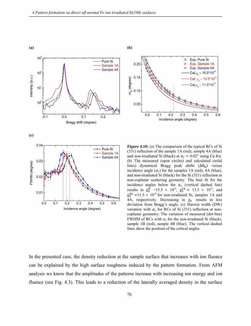
76
(a)
(b)
(c)
Figure 4.10: (a) The comparison of the typical RCs of Si
(331) reflection of the sample 1A (red), sample 4A (blue)
and non-irradiated Si (black) at 0.02° using .
(b) The measured (open circles) and calculated (solid
lines) dynamical Bragg peak shifts ( versus
incidence angle ( ) for the samples 1A (red), 4A (blue),
and non-irradiated Si (black) for the Si (331) reflection at
non-coplanar scattering geometry. The best fit for the
incidence angles below the (vertical dashed line)
results in =15.5 10
-6,
13.5 10-6
, and
11.5 10
-6 for non-irradiated Si, samples 1A and
4A, respectively. Decreasing in results in less
deviation from Bragg’s angle. (c) Darwin width (DW)
variation with for RCs of Si (331) reflection at non-
coplanar geometry: The variation of measured (dot-line)
FWHM of RCs with i for the non-irradiated Si (black),
sample 1B (red), sample 4B (blue). The vertical dashed
lines show the position of the critical angles.
In the presented case, the density reduction at the sample surface that increases with ion fluence
can be explained by the high surface roughness induced by the pattern formation. From AFM
analysis we know that the amplitudes of the patterns increase with increasing ion energy and ion
fluence (see Fig. 4.3). This leads to a reduction of the laterally averaged density in the surface
4 Pattern formation on direct off-normal Fe ion irradiated Si(100) surfaceswerden soll.

77
layer, although a considerable amount of Fe is incorporated. The observed net reduction of the
surface density of sample 1A leads to the conclusion that the process of pattern formation could
be already started at a Fe fluence of ~ 1016
ions cm-2
. At this early stage of pattern formation
surface roughening and the amorphization of silicon, that is also known to reduce the density
further by about 2% [91], are the main effects.
The net reduction of the surface density was examined for the samples irradiated with low ion
energy of 2 KeV with low ion fluences of 5 1014
ions cm-2
(less than 1ML) and 5 10
16 ions
cm-2
, named as samples 1C and 4C.
Fig. 4.11(a-b) shows the AFM images of the samples 1C and 4C, respectively. The RMS
roughness varies from 0.2 nm for the sample1C to 0.96 nm for the samples 4C.
Fig. 4.11c shows a comparison between the RCs of Si(331) reflection for the samples 1C (red
curves) and 4C (blue curves) at typical incidence angles of 0.45° (square-line), 0.2° (triangle-line)
and 0.02° (circle-line). It can be seen that by decreasing incidence angle the deviation from the
Bragg peak position decreases from the sample 1C to sample 4C.
Fig. 4.11d shows the variation of the measured Bragg shift as a function of incidence angle
for the sample 4C (open blue circles) and samples 1C (open red circles) and non-irradiated Si
(open black circles). For the sample 1C with smooth surface, variation of the Bragg shift with
incidence angle is almost the same as non-irradiated Si. This implies that there is a threshold
value of ion fluence for surface density modulation. For the sample 4C, the amount of Bragg shift
is smaller than non-irradiated Si when the incidence angles falls below the critical angle. The fit
of the calculated solid curve (blue curve) for angles below the critical angles give raise to =
12.47 10-6
for the sample 4C which is correspond to a surface density of = 1.95 g/cm3
(16 %
smaller than non- irradiated Si with = 2.32 g/cm3).
4.3 Depth density profiling of Si(100) after irradiation with Fe ions

78
(a)
(b)
(c)
(d)
Figure 4.11: AFM images of Si surfaces irradiated with 2 keV Fe ions at 65° incident angle with respect to the
surface normal at different fluences: (a) Sample 1C (zmax = 4.0 nm, = 0.28 nm) at 5 1014
ions cm-2
. (b) Sample
4C (zmax = 8.2 nm, = 0.96 nm) at 5 1016
ions cm-2
. The z is the height difference corresponding to the color
scale range. The imagines size is 3 × 3 µm2. (c) The comparison of the typical RCs of Si (331) reflection of the
sample 1C (red), sample 4C (blue) at 0.45° (cubic-line), 0.2° (triangle-line), and 0.02° (circle-line)
using . (d) The measured (open circles) and calculated (solid lines) dynamical Bragg peak shifts ( versus
for the samples 1C (red), 4C (blue), and non-irradiated Si (black) for the Si (331) reflection at non-coplanar
scattering geometry. The best fit for the incidence angles below the (vertical dashed line) results in =
=15.5 10
-6, and
12.47 10-6
for non-irradiated Si, samples 1C and 4C, respectively. Decreasing in results in less deviation from Bragg’s angle.
4 Pattern formation on direct off-normal Fe ion irradiated Si(100) surfaceswerden soll.

79
4.3.3 Extremely asymmetric diffraction with changing the wavelength
The alternative method to achieve EAD is tuning the photon energies at fixed coplanar scattering
geometry (see subsection 3.3) [92]. This method also was applied for the samples 1A, 4A and
non-irradiated Si as a reference. In order to get Si (311) reflection in EAD geometry, the photon
energies have been chosen in the range of 8550 eV up to 8875 eV providing the incidence angle
of X-ray on the surface between 1° and 0°. Due to the small incidence angles, the X-ray beam
simultaneously illuminates the surface of the sample as well as the sample’s edge. Fig. 4.12a
shows the RCs for the sample 4A at = 8715 eV (black), = 8810 eV (magenta), = 8840
eV (olive), = 8860 eV (red) and = 8875 eV (blue). Each RC consist of an intense sharp
peak at zero position of Bragg shift axis which corresponds to a Si (311) reflection where the
edge of the sample is illuminated and a broader peak at the right side which corresponds to the
reflection from the surface. With increasing photon energy consequently decreasing (see Fig.
3.7d), the surface peak starts to shift from kinematical Bragg angle and tends towards at higher
energies due to the increase of dynamical Bragg peak shift (Eq. 3.30). The “edge peak” is used as
a reference for the evaluation of the measured shifts of the surface peaks. Concurrent with the
deviation from Bragg’s angle, the intensity of the surface peaks drops exponentially by increasing
photon energy due to an exponentially reduction of the penetration depth (Fig. 3.7b).
Fig. 4.12b shows the map of corresponding measured RCs versus wavelength and the shift in
component of scattering vector ( for sample 1A. The intense sharp straight peak fixed at
the zero position of corresponds to the “edge peak” and the broader line with increasing peak
separation corresponds to the reflections from the surface. It can be seen that by decreasing
wavelength from λ = 1.45 nm ( = 8550 eV) to λ = 1.397 nm ( = 8875 eV resulting in a
decrease in incidence angle from 1° to 0°, increases accordingly. When the wavelength
becomes smaller than λ = 1.408 nm ( = 8805 eV), incidence angle becomes below the critical
angle ( 0.22°), as shown by vertical dashed line, and becomes measurable. Fig. 4.12c shows
the calculated RCs of Si (331) reflection at λ = 1.4238 nm ( = 8715 eV) to λ = 1.407 nm ( =
8810 eV , λ = 1.4027 nm ( = 8840 eV), λ = 1.3995 nm ( = 8860 eV), for pure Si(100) using
Sergey Stepanov X-ray server base on dynamical theory of X-ray diffraction with black, magenta,
olive, red, and blue curves, respectively.
4.3 Depth density profiling of Si(100) after irradiation with Fe ions

80
(a)
(b)
(c)
(d)
Figure 4.12: Deviation from Bragg’s angle of Si (311) reflection in coplanar scattering geometry by changing X-ray
wavelength: (a) The measured rocking curves (RCs) of Si (311) reflection versus Bragg peak shift for sample
1A at different photon energies of 8715 eV (black), 8810 eV (magenta), 8840 eV (olive),
8860 eV (red), and 8875 eV (blue). (b) The corresponding map of the measured RCs versus
wavelength/incidence angle and component of scattering vector ( . (c) The calculated RCs of Si (311) reflection
versus Bragg peak shift for Si at different photon energies ranging from 8715 eV to 8875 eV as inset using
Sergey Stepanov X-ray server base on dynamical diffraction theory. (d) The corresponding map of the calculated
RCs versus wavelength/incidence angle and component of scattering vector ( .
4 Pattern formation on direct off-normal Fe ion irradiated Si(100) surfaceswerden soll.

81
A vertical dashed line at the left side is corresponded to position of edge reflection. It can be seen
that there is a good agreement between calculated curves and measured ones (Fig. 4.12.a).
The Fig. 4.12d shows the map of corresponding calculated RCs versus wavelength and the
shift in component of scattering vector ( for pure Si at 311 reflections. The dashed line
fixed at the zero position of corresponds to the “edge peak” position and the broader line
with increasing peak separation corresponds to the reflections from the surface. By decreasing
wavelength (reducing ), increases and when the wavelength becomes closer to value
correspond to critical angle (λ = 1.408 ) becomes pronounced.
Fig. 4.13a shows a comparison between the measured RCs for the samples 1A (red), 4A
(blue) and non-irradiated Si (black) at =8840 eV ( = 0.08°). It can be seen that the deviation
from the Bragg peak position decreases from the non-irradiated Si over sample 1A to sample 4A
caused from reduction of the surface density. Quantitatively, these density variations can be
determined by fitting the measured Bragg peak shifts according to Eq. (3.30). Fig. 4.13b shows
the measured (open circle) and calculated (solid lines) dynamical Bragg-peak shifts ( ) versus
X-ray wavelength/incidence angle for the samples 1A (red), 4A (blue) and non-irradiated Si
(black). After calibrated to radiation, the fitting of the peak shifts reveals the
polarizabilities of = 13.49 10
-6 and
= 11.48 10-6
for the samples 1A and 4A,
respectively. These values are in good agreement with obtained results for the samples using
EAD at non-coplanar scattering geometry for Si (331) reflection (see subsection 4.3.2).
Fig. 4.13c shows a comparison between the measured RCs for the samples 1C (red) and 4C
(blue) and non-irradiated Si (black) at =8875 eV ( = 0.02°). While there is no pronounced
change in Bragg shift deviation of sample 1C compared to non-irradiated Si, this deviation
becomes considerable for the sample 4C because of a surface density reduction. Fig. 4.12d shows
the measured (open circle) and calculated (solid lines) dynamical Bragg-peak shifts ( ) versus
X-ray wavelength/incidence angle for the samples 1C (red), 4C (blue) and non-irradiated Si
(black). The fitting of the peak reveals a polarizability of = 12.47 10
-6 for the samples 4C.
This value is in good agreement with obtained results for the samples using EAD at non-coplanar
scattering geometry for Si (331) reflection (see subsection 4.3.2).
4.3 Depth density profiling of Si(100) after irradiation with Fe ions

82
(a)
(b)
(c)
(d)
Figure 4.13: (a) The comparison of rocking curves (RCs) of Si (311) reflection for the samples 1A (red), 4A (blue),
and non-irradiated Si (black) at = 8840 eV ( = 0.08°). (b) The measured (open circles) and calculated (solid
lines) dynamical Bragg peak shifts ( versus wavelength/incidence angle for the samples 1A (red), 4A (blue) and
non-irradiated Si (black). (c) The comparison of rocking curves (RCs) for the samples 1C (red), 4C (blue), and non-
irradiated Si (black) at = 8875 eV ( = 0.02°). (d) The measured (open circles) and calculated (solid lines) Bragg
peak shifts ( versus wavelength/incidence angle for the samples 1C (red), 4C (blue) and non-irradiated Si
(black). The best fit for incidence angles below the (vertical dashed line) results in = 15.48 10
-6,
= 13.49
10-6
, = 11.48 10
-6 ,
= 15.48 10-6
, and
= 12.48 10-6
for the non-irradiated Si, samples 1A and 4A,
1C, and 4C at = 1.54 , respectively.
4 Pattern formation on direct off-normal Fe ion irradiated Si(100) surfaceswerden soll.

83
Summary and discussion
In this chapter we reported on the pattern formation on Si surfaces under direct Fe ion
bombardment at 5 and 20 keV ion energies and at a 65° incidence angle with respect to the
surface normal with ion fluences ranging from 1 1016
to 5 1017
ions cm-2
. The morphologies
of the surfaces were investigated by AFM and TEM measurements showing that the ripple
formation occurs if the ion fluences exceeds 1 1016
ions cm-2
and the specific properties of the
formed ripples (wavelength and amplitude) on the surfaces vary by variation of ion beam
parameters (ion fluence and ion energy). In order to understand the mechanism of the pattern
formation, nondestructive X-ray methods were applied to identify the active material parameters
affecting the pattering mechanism. The surface density variation as a function of ion beam
parameters was investigated.
To this aim the conventional X-ray reflectivity (XRR) method was used. It showed the
formation of a few nm sub-surface layers with incorporated Fe ions in the case of smooth
surfaces. For the patterned surfaces the strong decay in the reflected intensity makes a detailed
evaluation impossible and with no pronounced variation at the critical angle and hence surface
density is observed, due to the competing effects from surface roughness and metal incorporation.
In order to improve the surface sensitivity, the extremely asymmetric X-ray diffraction (EAD)
method was applied. The access to very small incidence angles of X-ray ( even below the
critical angle makes the EAD method extremely surface sensitive. Depth profiling was achieved
by measuring X-ray rocking curves as a function of the decreasing incidence angles down to zero
degrees in non-coplanar scattering geometry using radiation, and in coplanar geometry
scattering by varying wavelengths using synchrotron radiation. The density information was
extracted from the variation of the dynamical Bragg peak shift with , and different critical
angles were extracted from the variation of the peak widths with . In contrary to the XRR, the
EAD revealed a net reduction of the surface density as a function of ion fluence and ion energy.
The density reduction at the patterned surfaces increases with ion fluence, which can be
explained by the high surface roughness, induced by the pattern formation. This leads to a
reduction of the laterally averaged density in the topmost layer, although a considerable amount
of Fe is incorporated. The observed net reduction of the surface densities at the smooth surfaces
4 Summary and discussion

84
leads to the conclusion that the process of pattern formation could be already started at Fe fluence
of ~1016
ion cm-2
. This conclusion was tested for a lower ion fluence (51014
ion cm-2
)
confirming that there is a threshold for ion fluences leading to surface density modulation. Thus,
it can be concluded that systematical variation of surface density with irradiation parameters can
be considered as the important parameter related to the patterning mechanism.
4 Fehler! Verwenden Sie die Registerkarte 'Start', um Heading 1 dem Text zuzuweisen, der hier angezeigt
werden soll.
4 Pattern formation on direct off-normal Fe ion irradiated Si(100) surfaces
werden soll.
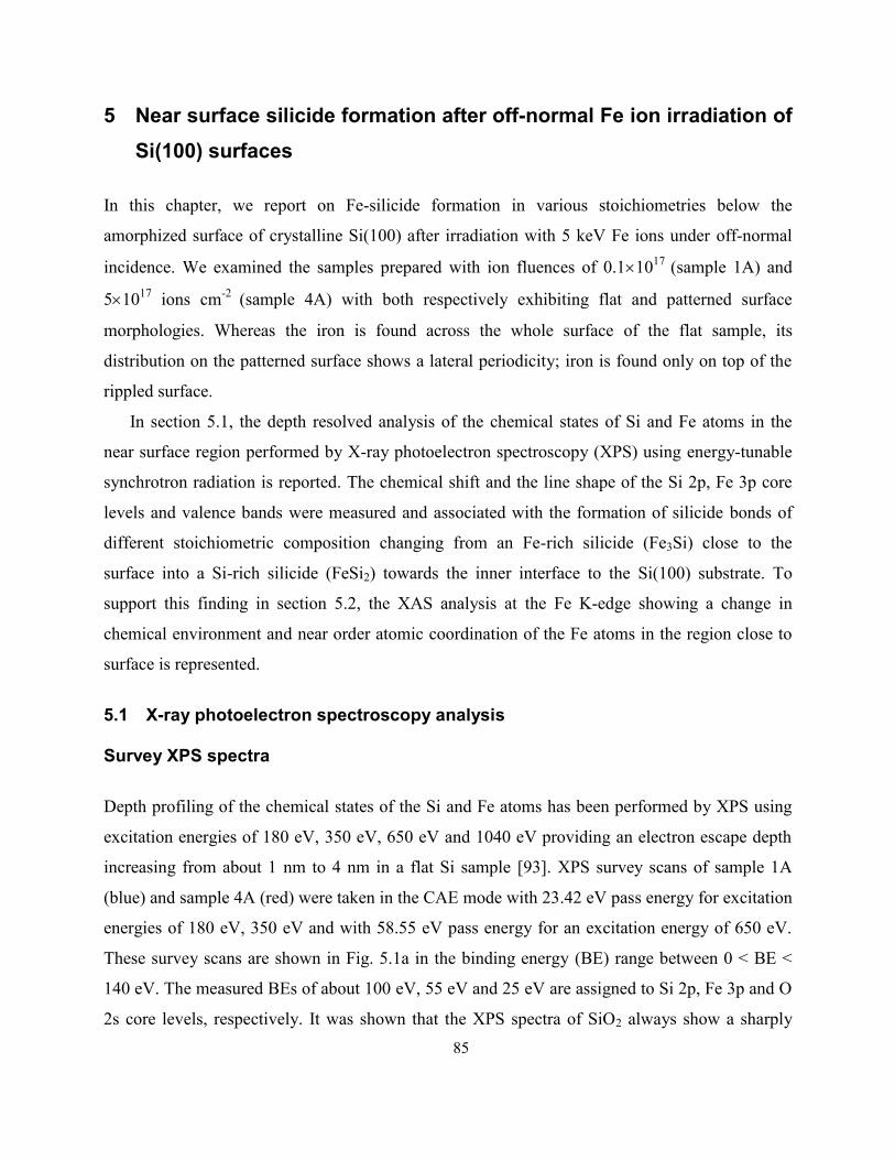
85
5 Near surface silicide formation after off-normal Fe ion irradiation of
Si(100) surfaces
In this chapter, we report on Fe-silicide formation in various stoichiometries below the
amorphized surface of crystalline Si(100) after irradiation with 5 keV Fe ions under off-normal
incidence. We examined the samples prepared with ion fluences of 0.11017
(sample 1A) and
51017
ions cm-2
(sample 4A) with both respectively exhibiting flat and patterned surface
morphologies. Whereas the iron is found across the whole surface of the flat sample, its
distribution on the patterned surface shows a lateral periodicity; iron is found only on top of the
rippled surface.
In section 5.1, the depth resolved analysis of the chemical states of Si and Fe atoms in the
near surface region performed by X-ray photoelectron spectroscopy (XPS) using energy-tunable
synchrotron radiation is reported. The chemical shift and the line shape of the Si 2p, Fe 3p core
levels and valence bands were measured and associated with the formation of silicide bonds of
different stoichiometric composition changing from an Fe-rich silicide (Fe3Si) close to the
surface into a Si-rich silicide (FeSi2) towards the inner interface to the Si(100) substrate. To
support this finding in section 5.2, the XAS analysis at the Fe K-edge showing a change in
chemical environment and near order atomic coordination of the Fe atoms in the region close to
surface is represented.
5.1 X-ray photoelectron spectroscopy analysis
Survey XPS spectra
Depth profiling of the chemical states of the Si and Fe atoms has been performed by XPS using
excitation energies of 180 eV, 350 eV, 650 eV and 1040 eV providing an electron escape depth
increasing from about 1 nm to 4 nm in a flat Si sample [93]. XPS survey scans of sample 1A
(blue) and sample 4A (red) were taken in the CAE mode with 23.42 eV pass energy for excitation
energies of 180 eV, 350 eV and with 58.55 eV pass energy for an excitation energy of 650 eV.
These survey scans are shown in Fig. 5.1a in the binding energy (BE) range between 0 < BE <
140 eV. The measured BEs of about 100 eV, 55 eV and 25 eV are assigned to Si 2p, Fe 3p and O
2s core levels, respectively. It was shown that the XPS spectra of SiO2 always show a sharply

86
pronounced O 2s peak [94, 95], which also appears in our survey spectra for all excitation
energies demonstrating the formation of a thin SiO2 layer on the surface.
Valence band (VB) spectra
The three peaks between 0-20 eV located at BE of about 1.5 eV, 7 and 11.5 eV named A, B, and
C, respectively, correspond to the VB distribution (see Fig. 5.1a). Fig. 5.1b shows the high
resolution VB spectra of samples 1A (blue) and 4A (red) for an excitation energy of 180 eV. The
formation of oxidation states causes the increase in the intensity of peaks B and C [94, 95]. Peak
B can be attributed to the 2p band of oxygen chemically adsorbed at the Si surface to form SiO2
[94, 96-98], and is more pronounced for sample 4A, indicating a higher degree of oxidation due
to the larger surface area. Furthermore, peak A which is absent in pure Si (not shown) can be
attributed to a modified Fe 3d density of states caused by silicide formation [99]. This broad
peak covering a BE interval between 0.6 and 2 eV can be used as a fingerprint of Fe-rich silicide
bonds formed close to the surface area [100-104]. Consequently, the amount of Fe-rich silicide
bonds at the top part of the surface is larger for sample 2 compared to sample 1, indicating a
higher amount of iron silicide in the surface of sample 4A. It was shown that Fe3Si starts to form
only after a critical dose of the deposited Fe exceeds a thickness of 0.43 nm [100, 102]. Thus,
the thickness of Fe rich layers in samples 1A and 4A (see Figs. 4.6-7) are already higher than this
threshold value. Furthermore, although the two presented valence band spectra in Fig. 5.1b are
overall quite similar, the higher intensity of peak A for sample 4A suggests a larger amount of
Fe-silicide formation for this sample, which agrees qualitatively with the results of the RBS
measurements.
5 Near surface silicide formation after off-normal Fe ion irradiation of Si(100) surfaces
werden soll.

87
(a)
(b)
Figure. 5.1:(a) Wide-scan X-ray photoemission spectra of Si(100) irradiated with 5 keV Fe ions incident at 65° with
respect to the surface normal at different fluences of 1 1016
ions cm-2
, sample 1A (blue), and 5 1017
ions cm-2
,
sample 4A (red), for excitation energies of 180 eV, 350 eV and 650 eV from top to bottom, respectively. The pass
energy for survey scan is 23.42 eV with spectrometer resolution ca. 0.5 eV. (b) XPS valence band spectra of the
sample 1A (blue) and sample 4A (red) at h = 180 eV. The pass energy is 2.33 eV with spectrometer resolution less
than 0.1 eV. See text for explanation of peaks A, B and C.
Si 2p XPS spectra
It is known that the Si 2p core levels in Fe-silicides are shifted towards higher binding energies
with respect to pure silicon for increasing Fe concentration [105]. This functional behavior was
applied to evaluate high resolution XPS measurements taken in the vicinity of the Si 2p core level
for samples 1A and 4A using different excitation energies.
Figs. 5.2a-d show the Si 2p core level spectra of sample 1A (full points) and sample 4A (open
circles) for excitation energies of 180 eV, 350 eV, 650 eV and 1040 eV, respectively. Each
spectrum was fitted by a Shirley type background and Gaussian peak functions of different
energy and FWHM. In particular the FWHM of the Si 2p3/2 and Si 2p1/2 core levels are estimated
to be about 0.6 eV, 0.7 eV, 1.2 eV and 1.6 eV for excitation energies of 180 eV, 350 eV, 650 eV
and 1040 eV, respectively.
5.1 X-ray photoelectron spectroscopy analysis

88
The measured profiles can be fitted by four peaks (red and blue curves in Fig. 5.2). The two
peaks at about 103.8 eV and 102.5 eV are assigned to SiO2 and a silicon suboxide SiO2-x,
respectively [106]. Those compounds will always form due to the air exposure of the samples
after removal from the irradiation chamber. The other two peaks close to 100 eV can be ascribed
to the spin-orbit splitted levels of Si 2p3/2 and Si 2p1/2. In the case of silicide bond formation these
two peaks experience a peak shift with respect to pure Si expected at 99.4 eV and 100.1 eV,
respectively. For both samples, the intensity of the peaks assigned to SiO2 increases with
decreasing excitation energy, while that attributed to Si 2p decreases, indicating the formation of
SiO2 on top of the surfaces. While the position of the SiO2 peak is independent from the
excitation energy, the peak intensity is higher for sample 4A compared to sample 1A indicating a
higher degreee of oxidation due to the rippled surface of sample 4A. This is in agreement with
the valence band peak B of both samples (see Fig. 5.1b).
The measured Si 2p3/2 and Si 2p1/2 core levels peaks are originating from photoelectrons of
pure silicon and various silicides. In order to quantify the contribution of silicides, both peaks
were fitted by Gaussians. Compared to pure silicon the peak maxima of the fitted Gaussians
always show a shift towards higher BE with a larger amount for sample 1A (fitted red curves)
compared to sample 4A (fitted blue curves) at excitation energies of 180 eV, 350 eV and 650 eV.
The inset of Fig. 5.2a shows the magnification of Si 2p3/2 and Si 2p1/2 core levels for sample 1A
(red curves) and sample 4A (blue curves) for an excitation energy of 180 eV. It highlights a
smaller peak shift of sample 4A compared to sample 1A which is accompanied by a larger
intensity of the Si 2p3/2 and Si 2p1/2 core level peaks due to the higher amount of Fe-silicide as
revealed from valence band spectra (see Fig. 5.1b). Qualitatively similar shifts are observed for
excitation energies of 350 eV and 650 eV but with decreasing magnitude. The peaks of both
samples nearly coincide for an excitation energy of 1040 eV. Comparing the four excitation
energies, the determined BEs of Si 2P3/2 core levels are 99.65 eV, 99.83 eV, 99.89 eV and 99.63
eV for sample 1A and 99.49 eV, 99.63 eV, 99.71 eV and 99.60 eV for sample 4A using
excitation energies of 180 eV, 350 eV, 650 eV and 1040 eV, respectively, measured from the
peak maxima of the fitted Gaussians.
5 Near surface silicide formation after off-normal Fe ion irradiation of Si(100) surfaceswerden soll.

89
(a)
(b)
(c)
(d)
Figure. 5.2. Comparison of Si 2p core level spectra of Si(100) irradiated with 5 keV Fe ions incident at 65°
with respect to the surface normal at different fluences of 1 1016
ions cm-2
, sample 1A, with measured data
(open circles) fitted by a Shirley type background (continuous red curves), and 5 1017
ions cm-2
, sample 4A,
with measured data (full circles) fitted by a Shirley type background (continuous blue curves): at h = 180 eV
(a), h = 350 eV (b), h = 650 eV (c), and h = 1040 eV (d). The inset in (a) shows the magnification of the Si
2p core level spectra in the vicinity of silicide bond for both samples.
Fig. 5.3 shows the variation of the BE of Si 2p3/2 core levels of sample 1A (red) and sample 4A
(blue) as a function of excitation energies and the respective electron escape depth. For
comparison the BE of various silicides and pure silicon are shown as well (horizontal dashed
lines). The top axis indicates the photo electron escape depth as estimated for pure silicon in case
5.1 X-ray photoelectron spectroscopy analysis

90
of a flat surface. The measured peak shift is maximum for excitation energies between 350 eV
and 650 eV.
Considering the increase of the electron escape depth for increasing excitation energies (see
subsection 3.4.2), the measured shifts for sample 1A follows qualitatively the decreasing Fe
content from top towards the bulk. This becomes understandable assuming nearly uniform
distribution of Fe along the flat surface. The situation is much different for sample 4A where the
silicides are accumulated at the top of the ripples. Although the integral Fe content is higher
compared to sample 1A (higher peak intensities), the measured peak shift is always smaller (by
about 0.15eV). The striking argument for the reduction of BE in sample 4A is an inhomogeneous
distribution of Fe across the surface seen in Fig. 4.7a. So, the measured photoelectrons are
originating simultaneously from the Fe-rich silicon ridges and almost pure silicon in the side-
walls and valleys. As the BE of Si 2p core levels in pure Si is lower than those of most of the Fe-
silicides [105], the contribution of Si atoms from side-walls and valleys leads to a systematic
reduction in BE of sample 4A with respect to sample 1A for excitation energies up to 650 eV.
Therefore qualitatively the blue curve in Fig 5 can be interpreted in similarly to sample 1A, i.e. in
the silicide regions the Fe content decreases from surface towards the bulk. For the highest
excitation energy (1040 eV) the contribution of underlying bulk Si dominates for both samples
independently from the surface pattern but is still influenced by the iron which is in good
agreement with results of Sánchez-García et al. reporting a similar chemical state for Si 2p3/2
using a X-ray source (1253.6 eV) [107].
5 Near surface silicide formation after off-normal Fe ion irradiation of Si(100) surfaces
werden soll.

91
Figure. 5.3. Binding energies of Si 2p3/2 core level as a function of excitation energies and electron escape depth
(upper x-axis assuming a pure Si surface) in Si(100) irradiated with 5 keV Fe ions incident at 65° with respect to the
surface normal at different fluences of 1 1016
ions cm-2
, sample 1A (red), and 5 1017
ions cm-2
, sample 4A (blue).
Olive dashed horizontal lines indicate the reported BE of Si 2p3/2 core levels for Fe3Si (99.6 eV), FeSi (99.7 eV),
FeSi2 (99.8 eV) and Si (99.4 eV) [105].
Fe 3p XPS spectra
The kind of chemical bonding between Si and Fe atoms can also be deduced from both the line
shape and the shift of the Fe 3p core levels [105, 108]. It was shown that the modulation in the
VB due to the formation of different stoichiometric composition of Fe-silicides has a direct
influence on the shape and energetic position of the Fe 3p peaks [109, 110].
The BE of the Fe 3p core levels were measured at different excitation energies. Because of
the formed SiO2 layer on top of the surface the intensity of the Fe 3p photoelectron peak at 180
eV is very low (see Fig. 5.1a). Thus high resolution Fe 3p core levels spectra of samples 1A and
4A are measured at excitation energies of 350 eV and 650 eV and are compared in Figs. 5.4a-d.
All spectra look asymmetric with a wider slope towards higher BEs. This is attributed to the
contribution of silicides with different Fe content that are enhanced close to the surface.
Following this assumption, the Fe 3p core level spectra were decomposed into two contributions
of Fe-Si bonds. The fitted peaks located at BE = 53.75 eV (red curves) can be attributed to
5.1 X-ray photoelectron spectroscopy analysis

92
silicides with high Fe contents such as Fe3Si [109, 111]. The Gaussian width ( 1.7 eV) of this
peak was kept fixed and the remaining part of the experimental curves were fitted by a second
Gaussian (green curves), approximating the BE of the other stoichiometry, such as FeSi and
FeSi2.
It turns out that the photoelectron intensity taken from sample 4A is higher compared to
sample 1A which refers to the higher content of implanted Fe. In addition, the relative
contribution of Fe3Si to the photoelectron peak is larger in sample 4A. This means that in the
ridges of the rippled surface a higher part of Fe atoms is bond in this Fe rich stoichiometry which
could be easily explained by the lateral periodicity of the iron concentration. On the other hand,
the asymmetry of the photoelectron peak towards higher BE is always larger for 650 eV
excitation energy compared to 350 eV which reflects the silicide distribution with decreasing Fe
amount towards the depth.
5 Near surface silicide formation after off-normal Fe ion irradiation of Si(100) surfaces werden soll.

93
(a)
(b)
(c)
(d)
Figure. 5.4. The measured Fe 3p core level spectra of Si(100) irradiated with 5 keV Fe ions incident at 65° with
respect to the surface normal at different fluences of 1 1016
ions cm-2
(sample 1A) and 5 1017
ions cm-2
(sample
4A) at different excitation energies: (a) sample 1A (dot-line) at h = 350 eV , (b) sample 1A (dot-line) at h = 650
eV, (c) sample 4A (triangle-line) at h = 350 eV , and (d) samples 4A (triangle-line) at h = 650 eV. After
substraction of a Shirley type background, the measured data were fitted by two Gaussians (blue sum curves). The
obtained red curves correspond to the Fe3Si and the green curves correspond to the other Fe-silicides.
5.1 X-ray photoelectron spectroscopy analysis

94
5.2 X-ray absorption spectroscopy (XAS) analysis
For a depth resolved characterization of the chemical state and the atomic near order of the Fe
atoms XAS measurements have been performed in the vicinity of the Fe K-edge at 7112 eV. The
penetration depth was tailored by varying the incidence angle of X-ray beam (in) from 0.01° <
c = 0.22° to 0.5° c (critical angle of total external reflection of Si) with respect to the sample
surface. Magnified views of the X-ray absorption near edge structure (XANES) of the samples
1A and 4A are presented in Figs. 5.5a-b. For comparison, XANES reference spectra of Fe3Si,
FeSi, FeSi2, are shown in Fig. 5.5c. As characteristic feature, they display a shift of the absorption
maximum towards lower photon energy for increasing Fe concentration in the silicide, i.e. from
Fe3Si over FeSi to FeSi2. Qualitatively, similar shifts are observed for sample 1A and 4A where
the feature of Fe3Si is more pronounced at sample 4A compared to sample 1A. The measured
spectrum taken at in = 0.01° (black curves in Figs. 5.5a-b) shows its maximum at a lower photon
energy compared to the spectrum taken at in = 0.5° (blue curve). Because a lower in
corresponds to a lower average X-ray penetration depth, this observation is an additional proof
for the appearance of Fe-rich silicides in the near surface region, and the dominance of a Si-rich
silicide for larger depth. More details of the data evaluation of XANES are presented elsewhere
[112].
5 Near surface silicide formation after off-normal Fe ion irradiation of Si(100) surfaces
werden soll.

95
(a)
(b)
(c)
Figure. 5.5: Comparison of normalized Fe K-edge XANES spectra at different X-ray incidence angles of 0.01°
(black) , 0.05° (red ) and 0.5° (blue) in Si(100) irradiated with 5 keV Fe ions incident at 65° with respect to the
surface normal at different fluences of (a) 1 1016
ions cm-2
(sample 1A), and (b) 5 1017
ions cm-2
(sample 4A).
(c) Comparison of the normalized XANES spectra at Fe K-edge of reference powder samples; Fe3Si (black), FeSi
(red) and FeSi2 (blue).
5.2 X-ray absorption spectroscopy analysis

96
Fig. 5.6a shows a comparison of normalized extended X-ray absorption fine structure (EXAFS)
spectra of sample 1A at in = 0.01° (black curve) and in = 0.5° (blue curve) with spectra of
sample 4A, (olive and gray curves), respectively. Reference spectra of Fe3Si, FeSi and FeSi2 are
shown in Fig. 5.6b. The peak maxima of both spectra located at 7.140 keV, 7.190 keV and 7.255
keV coincide well with those of the FeSi2 reference spectrum (blue curve in Fig. 5.6b). In other
words, the FeSi2 formation is dominant for larger depths for both samples independently of their
surface morphologies. By reducing the incidence angle to 0.01° the EXAFS spectrum of sample
1A fits closer to the Fe3Si reference spectrum (black curve in Fig. 5.6b) accompanied by a
pronounced shift towards lower photon energy in the edge region for sample 4A. This can be
attributed to an enhanced tendency to form Fe3Si silicide close to the surface at sample 4A.
For simulating the EXAFS spectra we assumed that the investigated samples consist of a
mixture of three reference compounds. Therefore we fitted the measured spectra by a linear
combination of Fe3Si, FeSi and FeSi2 reference spectra. The phase fractions were varied until
best agreement between the experimental and calculated spectra was achieved. Fig. 5.7(a-c)
shows selected fit results for sample 1A (red) and 4A (blue) for incidence angles of in = 0.05°,
in = 0.2° and in = 0.5°, respectively. For the fits, the energy scale of the EXAFS spectra were
transformed to a wave number (k) scale of the emitted photoelectrons by k = 2m(E-E0) / ħ
where E is the actual photon energy, E0 the edge energy, m the electron mass, and ħ=h
/2 Planck’s constant. The X-ray absorption fine structure (k) was extracted from the
experimental data by subtracting a smooth background function above the edge, and the data
were weighted by k2 in order to compensate the k-dependent fast decay of(k).
5 Near surface silicide formation after off-normal Fe ion irradiation of Si(100) surfaceswerden soll.
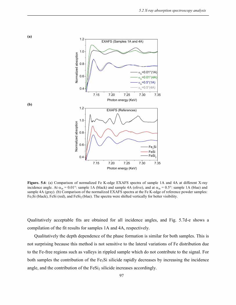
97
(a)
(b)
Figure. 5.6: (a) Comparison of normalized Fe K-edge EXAFS spectra of sample 1A and 4A at different X-ray
incidence angle. At in = 0.01°: sample 1A (black) and sample 4A (olive), and at in = 0.5°: sample 1A (blue) and
sample 4A (gray). (b) Comparison of the normalized EXAFS spectra at the Fe K-edge of reference powder samples:
Fe3Si (black), FeSi (red), and FeSi2 (blue). The spectra were shifted vertically for better visibility.
Qualitatively acceptable fits are obtained for all incidence angles, and Fig. 5.7d-e shows a
compilation of the fit results for samples 1A and 4A, respectively.
Qualitatively the depth dependence of the phase formation is similar for both samples. This is
not surprising because this method is not sensitive to the lateral variations of Fe distribution due
to the Fe-free regions such as valleys in rippled sample which do not contribute to the signal. For
both samples the contribution of the Fe3Si silicide rapidly decreases by increasing the incidence
angle, and the contribution of the FeSi2 silicide increases accordingly.
5.2 X-ray absorption spectroscopy analysis

98
(a)
(d)
(b)
(e)
(c)
Figure. 5.7: Exemplary results of the linear
combination (LC) fitting procedure of the X-ray
absorption fine structure spectra obtained for Si(100)
irradiated with 5 keV Fe ions incident at 65° with
respect to the surface normal at different fluencies of
1 1016
ions cm-2
(sample 1A), and 5 1017
ions cm-2
(sample 4A): measured spectra of sample 1A (dashed
red line) and sample 4A (dashed blue line) were fitted
(solid lines) for three different incidence angles of
0.05° (a), 0.2 (b) and 0.5° (c). Results of LC fitting of
sample 1A (d), and sample 4A (e) with different
amounts of Fe3Si, FeSi and FeSi2 as a function of
incidence angle.
5 Near surface silicide formation after off-normal Fe ion irradiation of Si(100) surfaces
werden soll.

99
In addition, it becomes possible to identify the amount and nature of Fe-Si bonds to the spectra.
This bond is present in larger amount in sample 4A which is in agreement with the Fe 3p XPS
spectra (see Fig. 5.4) showing a larger FWHM of Gaussians for the sample 4A in comparison to
sample 1A. Here it should be mentioned that neither in the Fe K-edge XANES and EXAFS
spectra (Figs. 5.5 and 5.6) nor in the Fe 2p (not shown) and Fe 3p photoemission spectra (Fig.
5.4) any effect of metal oxidation is observed. Therefore the formation of iron oxide is neglected
in our model. Furthermore, the fit quality generally decreases for smaller incidence angle. This is
mainly related to the fact that the footprint of the X-ray beam exceeds the actual sample size of
10 mm for incidence angles smaller than about i = 0.28°, reaching values of e.g. 28 mm for i =
0.1°, and even 57 mm for i = 0.05°. Thus the intensity of all measured signals decrease with
incidence angle, and the R factors of the fit (R=exp.(k)*k2) / fit.(k)*k
2) increase from about
0.08 – 0.09 for i = 0.2° and i = 0.5° to about 0.3 - 0.45 for i = 0.05°. Keeping in mind that the
photon statistics are substantially worse for the small incidence angles, however, this fit quality
appears reasonable.
Summary and discussion
Using XPS and XAS analyses, the chemical state and atomic coordination of Fe-silicides were
investigated in the nearly amorphized surface layer of crystalline Si(100), after irradiation with 5
keV Fe ions at oblique incidence angle. Two samples were prepared and studied with ion
fluences of 0.11017
, just below the threshold for pattern formation (sample 1A), and 51017
ions
cm-2
, just above this threshold (sample 4A). The Fe distribution in sample 1A is laterally uniform,
whereas it becomes laterally inhomogeneous in sample 4A in which the iron is concentrated in
the top region of the ripples at the sides facing the incident ion beam, as seen by TEM. Although
no crystalline silicide could be detected by X-ray diffraction [113], XPS and XAS revealed that
Fe is chemically bonded in a Si framework within a thin surface layer. Using both methods, it
was shown that the Fe concentration of these silicides changes with depth. The atomic
coordination is similar to a Fe-rich silicide at the outer surface, while a Si-rich silicide with a
structure similar to that of FeSi2 is found at inner interfaces towards the Si crystal.
5 Summary and discussion

100
The chemical depth profiles were deduced from the shift of the Si 2p3/2 core levels. Considering
a functional relationship between the core level shift and the chemical state of Si in different
silicide stoichiometry as taken from Ref. [105] (see olive dashed lines in Fig. 5.3), the Fe starts to
form silicides where the Si is coordinated by at least three Fe atoms close below the surface
(Fe3Si) and reaches FeSi2 stoichiometry at a larger depth. This depth dependence of the Fe
concentration is verified by XAS (Fig.5.7). At the surface, a dominant atomic coordination was
found similar to a Fe-rich silicide (Fe3Si), and the concentration of the lower stoichiometric
phases of Fe silicides (mainly FeSi2) is increasing towards the bulk penetration depths. For the
flat sample 1A, the Si-rich silicide (FeSi2) appears at a depth of about 3 nm, which is consistent
with TEM analysis (Figs 4.6-7) and reflectivity measurements [114] where a layer of high Fe
concentration of about 2.5 nm is visible.
The influence of the morphology on the obtained depth dependency can be directly deduced
from the results of the XAS measurements for sample 1A and 4A (Fig. 5.5) in comparison with
the TEM data (Fig. 4.6-7). A high concentration of Fe is present in one half of the ripple period
only. This Fe is accumulated on the side facets facing the ion beam with a thickness that is more
than a factor of 2 larger compared to the flat sample (~7 nm). Therefore the XAS spectra of both
samples (Fig. 5.7a-b) should show a different depths dependence due to the “laterally averaged”
information. However, taking these results into account it can be concluded that the pattern
formation is strongly influenced by the formation of Fe-silicides near the surface. Since the
different stoichiometry of Fe-silicides have different cohesive energies [115], they have different
surface binding energies and thus different sputter yields. In this context, the different sputtering
yields of silicon and iron and the inhomogeneous lateral distribution of iron has to be taken into
account. Therefore different areas along the surface will exhibit different sputter yields that
influence the process of ion beam erosion and may even lead to an enhancement of the processes
that are responsible for the ripple formation. This conclusion is in agreement with the predictions
of Bradley’s theory, in which a chemical reaction between impurity atoms and target atoms are
supposed to destabilize the surface as a precondition for ion induced pattern formation.
5 Near surface silicide formation after off-normal Fe ion irradiation of Si(100) surfaces
werden soll.

101
6 Recrystallization of Fe ion irradiated Si(100)
In the previous chapter, it was demonstrated that the irradiation of the Si(100) surfaces with Fe
ions at room temperature causes the formation of buried amorphous silicides with different
stoichiometries changing from a Fe-rich silicide (Fe3Si) at the topmost layer to a Si-rich silicide
(FeSi2) towards the bulk Si. Considering the fact that the near surface region is amorphous,
crystalline silicides were not observed using X-ray diffraction methods [113]. Therefore, a
thermal annealing process was applied to observe the recrystallization process of various
silicides.
In this chapter, the structural transition from amorphous to crystalline phase during annealing
process is described. To obtain information regarding the formed silicide phases and their spatial
distribution in the Fe-Si layer, grazing incidence X-ray diffraction (GI-XRD) measurements were
applied. We examined samples, prepared under off-normal irradiation with 20 KeV Fe ions at
different fluences of 0.11017
ions cm-2
(sample 1B) and 51017
ions cm-2
(sample 4B) exhibiting
a smooth and patterned surface morphology, respectively.
After a short review of the equilibrium phase diagram and preliminary crystallographic
properties of the Fe-Si binary system, the experimental procedure of the annealing process is
presented. In section 6.1, the effect of ion fluence on the formation of different silicide phases
during crystallization of an amorphous Fe-Si layer is investigated. In section 6.2, ion beam-
induced strain profiles before and after annealing are presented.
Preliminary crystallographic data
Fig. 6.1a shows the equilibrium phase diagram of the Fe-Si binary system [116]. Various iron
silicides with different physical properties are formed as a function of composition and
temperature. Some of iron silicide phases (Fe3Si, FeSi, and FeSi2) are reviewed.
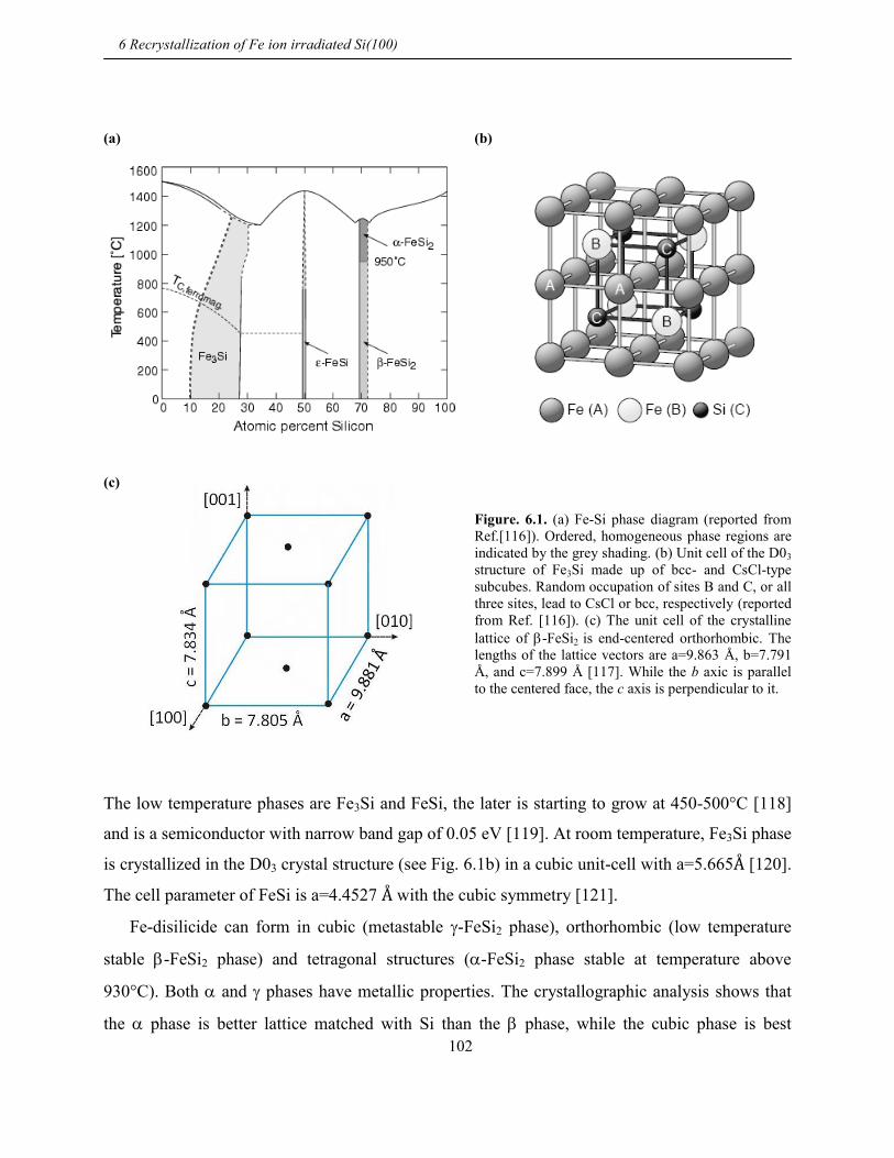
102
(a)
(b)
(c)
Figure. 6.1. (a) Fe-Si phase diagram (reported from
Ref.[116]). Ordered, homogeneous phase regions are
indicated by the grey shading. (b) Unit cell of the D03
structure of Fe3Si made up of bcc- and CsCl-type
subcubes. Random occupation of sites B and C, or all
three sites, lead to CsCl or bcc, respectively (reported
from Ref. [116]). (c) The unit cell of the crystalline
lattice of -FeSi2 is end-centered orthorhombic. The
lengths of the lattice vectors are a=9.863 Å, b=7.791
Å, and c=7.899 Å [117]. While the b axic is parallel
to the centered face, the c axis is perpendicular to it.
The low temperature phases are Fe3Si and FeSi, the later is starting to grow at 450-500°C [118]
and is a semiconductor with narrow band gap of 0.05 eV [119]. At room temperature, Fe3Si phase
is crystallized in the D03 crystal structure (see Fig. 6.1b) in a cubic unit-cell with a=5.665 [120].
The cell parameter of FeSi is a=4.4527 with the cubic symmetry [121].
Fe-disilicide can form in cubic (metastable -FeSi2 phase), orthorhombic (low temperature
stable -FeSi2 phase) and tetragonal structures (-FeSi2 phase stable at temperature above
930°C). Both and phases have metallic properties. The crystallographic analysis shows that
the phase is better lattice matched with Si than the phase, while the cubic phase is best
6 Recrystallization of Fe ion irradiated Si(100) werden soll.

103
matched with Si among the three FeSi2 phases, because of ac ≃ aSi=5.431 . In the case of -FeSi2
(a=b=2.695 and c=5.14 ), since 2a=5.390 , the lattice mismatch between -FeSi2 and Si
or cubic FeSi2 is only 0.7% along the a or b axis, as compared to a mismatch of ~ 2% for -FeSi2,
grown epitaxially on a Si(100) substrate [122].
The metastable FeSi2 phase transforms into the -FeSi2 phase upon annealing. The transition
temperature was found to decrease with increasing the thickness of the epilayer [123].
The semiconductor -FeSi2 phase is a narrow band gap (0.85 eV) semiconductor, and starts
to nucleate from FeSi at about 550°C, but a much higher temperature is needed for complete
crystallization of a -FeSi2 layer. The -FeSi2 phase is in equilibrium with Si at low temperature
[124]. Indeed the -FeSi2 phase is a rather peculiar semiconductor as its electronic structure is not
based on the SP3 hybridization, as it is the case for other common semiconductors (Si, Ge,
GaAs,…), but on a solid-state Jahn-Teller effect [125]. The unit cell of the end-centered
crystalline lattice of the -FeSi2 phase is shown in Fig. 6.1c [117].
Growth of thin iron silicide on silicon substrate
With very thin films, one observes usually the growth of strained and /or pseudomorphic phases,
adopting the substrate structure. Furthermore, in ultra thin films different crystalline phases are
observed in the entire composition range [116], which cannot be analyzed in terms of the bulk
phase diagram [126]. Their structures and physiochemical properties can be quite different from
those expected in the bulk phase diagram. For instance, the tetragonal -FeSi2 phase has been
reported to grow at a temperature (550°C) much lower than predicted value by the bulk phase
diagram (at 940°C). In addition, the formation of -FeSi2 in epitaxy with Si matrix with two type
of orientations (fully aligned and twinned with a same type of epitaxial relationship) at the Fe ion
implantation in Si(100) during crystallization at 320°C was observed [122, 127]. However, all of
them evolved towards the equilibrium phases with increasing thickness and temperature,
following equilibrium thermodynamic predictions.
Experimental procedure
Fehler! Verwenden Sie die Registerkarte 'Start', um Heading 1 dem Text zuzuweisen, der hier angezeigt
werden soll.
Growth of thin iron silicide on silicon substrate

104
Annealing of selected samples was performed in a vacuum chamber with pressure of 10-6
mbar.
The temperature was selected in the range between RT and 800°C in steps of 100°C. All the
samples were analyzed by X-ray diffraction (XRD) at grazing incidence angle (GI) geometry at
beamline ROBL at ESRF equipped with a six-circle goniometer and a linear detector. The GI-
XRD measurements were performed at a fixed incidence angle (in) in a step-scanning mode with
a step size of 0.1° for thermal annealing and 0.05° for depth profiling, using X-ray wavelength of
λ=1.078 Å. The annealing was carried out using DHS 900 Domed Hot Stage Anton Paar GmbH
attached to the goniometer equipped with TCU 150 temperature control unit. The heating rate
was kept ~ 5°C/min.
AFM analysis
Figs. 6.2(a-b) show the surface morphologies of the samples 1B and 4B after annealing. The
morphologies of the surfaces are similar with those before annealing (see Figs. 4.2a, d), except a
small variation in RMS roughness. While the surface of sample 1B remains smooth (Fig. 6.2a), it
changes to column like morphology for sample 4B (Fig. 6.2b).
Figure. 6.2. AFM images of Si surfaces irradiated with 20 keV Fe ions at 65° incident angle with respect to the
surface normal at different fluences: (a) Sample 1B (zmax = 4.83 nm, = 0.37 nm) at 1 1016
ions cm-2
. (b)
Sample 4B (zmax = 112.8 nm, = 14.52 nm) at 5 1017
ions cm-2
. The z is the height difference corresponding to
the colour scale range. The imagines size is 3 × 3 µm2.
(b) (a)
6 Recrystallization of Fe ion irradiated Si(100) werden soll.

105
6.1 Effect of ion fluence on the phase composition
6.1.1 Structural evolution in high-fluence Fe ion irradiated Si upon thermal
annealing
Fig. 6.3a shows the measured GI-XRD spectra of sample 4B, irradiated at fluence of 51017
ions
cm-2
, for different annealing temperatures starting at RT (gray), 400°C (black), 500°C (orange),
600°C (red), 700°C (olive), and 800°C (blue). While upto 400°C no diffraction peaks are
observed, at 500°C a small but sharp peak is appeared at 2 = 20.16° indicating the onset of
recrystallization of amorphous Fe-silicides. By increasing the annealing temperature up to 700°C
two additional broad peaks are appeared at 2 ~ 31.7° and 2 ~ 33.7° accompanied by increasing
intensity and width of the observed peak. These three peaks correspond to the diffraction peaks of
(220)/(202), (040) and (422) of the orthorhombic -FeSi2 phase [117, 121, 128]. The asymmetry
of the last two peaks indicates a trace of overlapping between the signals of FeSi2 and formed
FeSi phase as reported in Ref. [118]. As no reflection from non-reacted iron is detected, all
elemental iron is consumed by the growth of silicides, in agreement with X-ray absorption
analysis [112]. By increasing the annealing temperature to 800°C, a new small peak at 2 =
19.45° shows up. This peak is assigned to (110) reflection of -FeSi phase [118, 121]. The
formation of -FeSi and -FeSi2 phases in Fe ion impalanted Si has already reported in Refs.
[127, 129-131]. Katsumata et al. [132] reported also on formation of polycrystalline -FeSi and
-FeSi2 during annealing of Fe ion implanted Si(001) with differnet energies and fluences.
Fig. 6.3b shows the extracted FWHM of the (220) main reflection of -FeSi2 as a function of
annealing temperature1. It can be seen that by increasing the annealing temperature, the FWHM
decreases indicating of increasing in crystalline size. The particle size, t, was calculated using
Scherrer equation [133]:
t = 0.9λ / B cos B (6.1)
1 The FWHM of other reflections did not take into account because of difficulty in distinguish between the two
phases in these spectra.
6 Fehler! Verwenden Sie die Registerkarte 'Start', um Heading 1 dem Text zuzuweisen, der hier angezeigt
werden soll.
6.1 Effect of ion fluence on the phase composition

106
where λ is the wavelength of the used X-rays, B is usually measured, in radians, at an intensity
equal to half the maximum intensity and θB is the angle of diffraction. The inset of Fig. 6.3b
shows the variation of calculated particle size of the -FeSi2 phase along the (220) direction. It
can be seen that the average crystalline size increases from ~ 16 nm to ~ 28 nm by increasing
annealing temperature from 500°C to 800°C.
(a)
(b)
Figure. 6.3: (a) The measured GI-XRD spectra of the sample 4B (irradiated in off-normal with 20 KeV Fe ions at
fluence of 51017
ions cm-2
) at 800°C (blue), 700°C (olive), 600°C (red), 500°C (orange), 400°C (black), and room
temperature-RT (gray), taken at incidence angle of in=1° using λ=1.078 Å, and 2 =0.1°. (b) The variation of
FWHM of the -FeSi2 (220) reflection with annealing temperature. The insert shows the variation of crystallite size
with annealing temperature, calculated for -FeSi2 (220) reflection using Scherrer formula.
To obtain more information regarding the crystalline phases and their spatial distribution within
the formed silicide layer, the GI-XRD profiles were recorded at fixed temperature (T=800°C) as
a function of incidence angle varying in steps of 2 = 0.05°. The measured spectra at i = 0.2°, i
= 0.5° and i = 1° are shown in Fig. 6.4a from top to bottom, respectively. At all incidence angles
four pronounced peaks are appeared. The two peaks in lower angles with the symmetric shapes
6 Recrystallization of Fe ion irradiated Si(100)werden soll.
107
are assigned to -FeSi (110), and -FeSi2 (220)/(202), reflections [129]. The other two peaks in
higher angles are asymmetric in shape due to the overlapping between different reflections from
these two formed phases [128]. Using Gaussian fits (red and green curves in Fig 6.4a), it was able
to decompose these two asymmetric peaks into two main components. The green Gaussians at 2
= 31.7° and 33.89° are assigned to (210) and (211) reflections of the -FeSi phase, respectively
[118]. The red Gaussians at 2 = 31.84° and 33.78° are assigned to (040) and (422) reflections of
the -FeSi2 phase, respectively [118]. It is clear from Fig. 6.4a that the annealed sample consists
of both polycrystalline -FeSi and -FeSi2 phases, in which -FeSi2 is always dominant phase.
The larger the angle of incidence, the deeper the probed region of the sample. Therefore, the
fact that the peak intensities decrease with an increase of the angle of incidence is proof for the
silicide formation in the surface region. The observation of the more intense peaks at angular
positions of three main peaks of the and phases suggests that a kind of epitaxy growth
adjacent to the sample surface most likely was achieved.
Fig. 6.4b shows the variation of total integrated peak intensities associated with ε (green
columns) and (red columns) phases with incidence angle. While the integrated intensities of
both and phases increase by decreasing the incidence angle, the intensity ratio (I/ I) of both
peaks, as shown by dashed blue curve in Fig. 6.4b, increases from 18% at in=1° to 37.5% at
in=0.2° over 33.5% at in=0.5°. This implies that the -FeSi2 phase lies between -FeSi layer
and Si substrate. The formation of a periodic structure in Fe implanted Si(001) was also reported
previously [131]. This finding is in agreement with Ishimaru et al.[129], who reported on the
formation of the -FeSi2 layer between the topmost -FeSi layer and Si substrate. In other words,
the -FeSi2 phase is grown close to the inner region of bulk Si(001) which is in agreement with
the results of XPS and XANES analyses, showing the formation of Fe-silicides with higher Fe-
component on upper part of the ripples (see subsections 5.1 and 5.2).
The -FeSi2 lattice parameters were determined from the GI-XRD spectra for different
incidence angles. In table 6.1, these parameters are compared with the calculated values for the
bulk unstrained -FeSi2 [134] as reference. The strain εa, εb, and εc along the crystal axes are
calculated (εa = (a-a0) / a0, εb = (b-b0) / b0, εc = (c-c0) / c0) and given in table 6.1.
6.1 Effect of ion fluence on the phase composition 6.1 Effect of ion fluence on the phase composition

108
(a)
(b)
Figure. 6.4: (a) The measured GI-XRD spectra of the sample 4B (irradiated in off-normal with 20 KeV Fe ions at
fluence of 51017
ions cm-2
) at annealing temperature of 800 °C at X-ray incidence angle of 0.2° (up), 0.5° (middle),
and 1° (down) using λ=1.078 Å, and 2 =0.05°. (b) The variation of the total integrated intensities with incidence
angles, calculated for -FeSi2 (red) and -FeSi (green). The dashed blue curve is a fit curve over open circles,
indicating the variation of ratio of integrated intensity of -FeSi to -FeSi2 phases with incidence angles.
Table 6.1 Lattice parameters of -FeSi2 phase for the sample 4B at annealing temperature of 800°C, compared with
calculated values for bulk -FeSi2 lattice parameters. The strain: εa, εb and εc along the crystal axes are calculated
(εa=(a-a0)/a0, εb=(b-b0)/b0, εa=(c-c0)/c0) using the calculated values for bulk -FeSi2 lattice parameters from Ref. [134]
, as reference.
Phases a ( ) b ( ) c ( ) εa (%) b(%) c (%)
-FeSi/Exp 4.511 4.511 4.511 1.302
-FeSi/calculated (bulk) 4.453 4.453 4.453
-FeSi2/0.2° (Exp) 9.941 7.846 7.937 0.609 0.533 1.316
-FeSi2/0.5° (Exp) 9.963 7.851 7.913 0.834 0.601 1.00
-FeSi2/1° (Exp) 9.967 7.859 7.857 0.871 0.692 0.296
-FeSi2/calculated (bulk) 9.881 7.805 7.834
6 Recrystallization of Fe ion irradiated Si(100) werden soll.

109
It is seen that for all incidence angles, all lattice parameters are larger than the unstrained bulk
values. By decreasing the incidence angle, the strain in direction of c axic increases while in
directions of a and b axes decreases. A compression of c is expected due to the Poisson effect
when a expansion of a and b occures in an attempt to match the substrate lattice parameters [69,
135].
the calculated lattice parameter for the -FeSi pahse for (110) reflection is a = 4.511 for all
incidence angles that shows a strain of = 1.3 % in compare to bulk value 4.453 .
6.1.2 Structural evolution in low-fluence Fe ion irradiated Si upon thermal
annealing
Fig. 6.5a shows the GI-XRD spectra of sample 1B, irradiated at fluence of 11016
ions cm-2
, for
different annealing temperatures starting at RT (gray), 400°C (black), 500°C (orange), 600°C
(red), 700°C (olive), and at 800°C (blue). While upto 500°C no diffraction peaks are observed,
reaching 600°C the broadened diffraction peaks at the 2 ~ 31.7° and ~ 33.7° are appeared as a
onset of recrystallization of amorphous Fe-silicides. By increasing the annealing temperature to
700°C and 800°C, these peaks become larger in intensity. In order to increase the surface
sensitivity, the X-ray incidence angle was decreased close to the critical angle of total external
reflection of Si (c = 0.155° at λ = 1.078 ).
Fig. 6.5b shows the XRD spectra of this sample at 800°C at different incidence angles of 0.2°,
0.5°, 1° and 5° from top to bottom, respectively, measured with a step of 2 = 0.05°. At 5°
incidence angle, only one peak is appeared at 2 = 24.43°. This peak is assigned to ε-FeSi (111)
reflection. By decreasing the incidence angle to 1°, six peaks are appeared in the diffraction
spectra at the 2 = 20.45°, 24.35°, 26.55°, 29.08°, 31.80°, and 33.85° which are assigned to
β(220), ε(111), (111), β(023), β(040), and (211)/ β(422), respectively [118, 121]. At incidence
angle of 0.5°, all peaks increase in intensity accompanied by unusual broadening of β(023) peak.
This means that a particular orientation of β phase is dominance at the interface. By decreasing
the incidence angle to 0.2°, almost all peaks increase in intensity, indicating the formation of
crystalline silicides close to surface. The phase variation as a function of depth can be associated
with a change of the Fe concentration profile [127].
6.1 Effect of ion fluence on the phase composition
110
The appearance of ε-FeSi(111) reflection at sample 1B shows that different ion fluence or layer
thickness causes a critical variation of preferred orientation for ε-FeSi phase growth. A variation
in growth orientation by varying implanted Fe concentration was reported for cubic FeSi2 in Refs.
[122, 127].
_ENREF_27The peak at 2 = 26.543° (d = 2.348 ) is attributed to (111) reflection of -FeSi2
phase [128] which is absent in the sample 4B. The formation of -FeSi2 in our case can be
compared with results of Tan et al. [136]. He reported that Fe implantation with a fluence in (1-
3)1017
cm-2
range results in formation of the -FeSi2 phase, but the -FeSi2 phase is formed
only at a fluence about 51017
cm-2
. Upon annealing, the semiconducting -FeSi2 phase was
formed in Fe-implanted samples independent from the ion fluence [136].
One important difference between -FeSi2 and -FeSi2 phases is that the first one has a much
simpler crystal structure. Our observation suggests that the formation of -FeSi2 phase with a
simple structure is more favored than the thermodynamically stable -FeSi2 phase with an
orthorhombic structure when the ion fluence is low. Since the -FeSi2 can be considered as -
FeSi2 having disordered atomic positions [136], by increasing ion fluence -FeSi2 formation
dominants (no -FeSi2 peaks found at rough surfaces-see Fig. 6.4a).
6 Recrystallization of Fe ion irradiated Si(100) werden soll.

111
(a)
(b)
Figure. 6.5: (a) The measured GI-XRD spectra of the sample 1B (irradiated in off-normal with 20 KeV Fe ions at
fluence of 11016
ions cm-2
) at 800 °C (blue), 700 °C (olive), 600 °C (red), 500°C (orange), 400°C (black), and room
temperature-RT (gray) taken at incidence angle of in=1° with λ=1.078 Å, and 2 =0.1°. (b) GI-XRD spectra of the
sample 1B at annealing temperature of 800°C at incidence angle of 0.2°, 0.5°, 1°, and 5°, from top to bottom,
respectively, and 2 =0.05°.
6.2 Strain analysis
X-ray rocking curve analysis is a non-destructive technique for characterization of lattice strain.
By comparing with theoretical rocking curves, profiles of lattice strain can be evaluated. Fig. 6.6a
shows the rocking curves of Si(400) reflection of sample 1B at RT before (red curve) and after
(blue curve) annealing at T=800°C. Prior to annealing, the signal of the implanted layer shows a
shoulder on the low angle side of the substrate peak (but no fringes), indicating lattice expansion
of the irradiated region in a direction perpendicular to the surface. Lattice expansion may be
caused by interstitial and substitutional atoms as known from other X-ray studies of ion
implanted Si [137, 138].
Fig. 6.6b shows the simulated reflection pattern (solid black surve) in comparison to
measured (red open circles) one at room temperature. To simulate the strain as a function of
6.2 Strain analysis

112
depth the implanted region is divided into a number of thin lamellae in which the strain is kept
constant. The disordered parts of an ion implanted crystal may containe atoms which are
randomly displaced from their ideal lattice sites causing a reduction of the reflectivity. This
decrease of the X-ray reflectivity was taken into account considering a static Deby-Waller factor.
The simulated strain profile is illustrated as inset of Fig. 6.6b. It can be seen that the ion beam
induced strain reaches its maximum at the depth of around 5 nm below the surface and within a
thickness of 5 nm. This thickness is comparable with the penetration depth of Fe ions obtained
from X-ray reflectivity at room temperature (see inset of Fig. 4.8d ).
After annealing at 800°C, several fringes appear at the left and right sides of the Si (400)
reflection peak (see Fig. 6.6a). These fringes are caused by interference of X-rays reflected from
the surface and from a buried amorphous-crystalline interface [139]. The thickness of the strained
layer, t, may be determined from the angular distance of the interference fringes using the
equation [140]:
t = λ sin(2 B- ) / sin2 B (6.2)
where λ is the wavelength (1.078 ), the angle at which the period is measured and the
fringe period. A thickness of about 28 nm is calculated using the given formula. This reveals that
a thin film is formed during the annealing process.
The amount of average strain (neglecting the detailed depth dependence) can be determined
from the angular separation between the position of the lowest angle oscillation and the position
of the Si Bragg peak, using the equation [140]:
a/a = - / tan B (6.3)
where is the angle between the substrate peak and the peak of the strained layer, and B is the
Bragg angle (23.40° for the Si (400) reflection).
Fig. 6.6c shows the simulated reflection pattern (solid black curve) in comparison to
measured (blue open circles) one at room temperature after annealing at 800°C. The simulated
strain profile is illustrated as inset of Fig. 6.6c.
6 Recrystallization of Fe ion irradiated Si(100) werden soll.

113
(a)
(b)
Figure. 6.6: (a) Comparison of Si (400) reflection at
room temperature (RT) prior the annealing (red curve),
and after the annealing at 800°C (blue curve) for the
sample 1B (implanted with 20 KeV Fe ion under 65°
incidence angle with 11016
ions cm-2
). (b) The Si (400)
reflection of sample 1B at RT (open red circles) and
simulated curve (black solid curve). The insert shows the
extracted strain profile. (c) The Si (400) reflection of
sample 1B at RT after annealing at 800°C (open blue
circles) and simulated curve (black solid curve). The
insert shows the extracted strain profile.
(c)
It seems that the recrystallization of amorphous Si between silicides and bulk Si substrate can be
leads to such a modulation on reflection pattern. This interpretation can be confirmed by TEM
analysis (see Fig. 4.6a ) showing an amorphous bilayer consisting of amorphous Fe-Si and
amorphous Si layers, formed on bulk Si. Furthermore, the recrystallization of amorphous Si in
the case of high Fluence Fe implanted Si after annealing at 600°C has already been reported by
Naito et al. [141], showing the formation of a periodic structure of recrystallized buried Si and
silicide with different structure compared to the structure of a topmost layer.
6.2 Strain analysis

114
Summary and discussion
In summary, the crystallization process of the amorphous Fe-Si layers, formed by a low and high
fluence Fe ion irradiation on Si(100) substrates, was examined. The crystallization process was
carried out by thermal annealing in which the samples were annealed in the range of RT and
800°C and characterized by GI-XRD during annealing.
Comparing the XRD spectra of a smooth surfac (low ion fluence) and a patterned surface
(high ion fluence) shows that in the former case, the crystallization starts at a higher annealing
temperature compared to the later one starting at 500°C. This can be related to the different
thicknesses of a formed Fe-Si layer on the samples.
The depth profile of the recrystallized Fe-silicides was probed by grazing incidence X-ray
diffraction. It revealed that the silicide with higher Fe content (ε-FeSi) is formed close to the
surface, and changes to a lower Fe content phase (-FeSi2) at larger depths. While the
polycrystalline -FeSi2 phase dominates at the irradiated sample with higher ion fluence, a nearly
equal ratio between ε-FeSi and -FeSi2 phases is found at irradiated sample with lower ion
fluence. The formation of two equilibrium FeSi and FeSi2 phases was reported by Desimoni at al.
[131], and their formation temperatures are slightly dependent on the layer thicknesses.
These findings for crystallized silicides are in agreement with the findings by XPS and XAS
analyses on amorphous silicides formed on the as-irradiated samples (see chapter 5), showing a
formation of Fe-rich silicide (Fe3Si) on the topmost layer changing to Si-rich silicide (FeSi2)
towards buried layers. Here it should be mentioned that the Fe3Si phase is stable at low
temperatures and can not survive at high annealing temperatures.
These findings confirm that small silicides moieties are already formed during the irradiation
process. Furthermore, various formed phases are distributed with different ratios within a Fe-Si
layer at low and high fluence Fe ion irradiated Si. This suggests that the resulting density
inhomogeneity along the surface can be considered as the relevant factor in the process of pattern
formation.
6 Recrystallization of Fe ion irradiated Si(100) werden soll.

115
7 Ion beam induced pattern formation on Si(001) with incorporation
of metal atom impurities
In this chapter it is shown that for a normal and near normal Kr ion incidence, a pattern formation
can be developed on Si(001) surfaces due to incorporation of metal impurities like Fe and Cr
atoms with a certain amount, offering a new degree of freedom for pattern control. However, to
understand the mechanisms being responsible for pattern formation in the presence of metallic
atoms, the depth profiling and the chemical state of the metal atoms is required.
In section 7.1, the pattern formation on Si(001) surface using a Kaufman type broad-beam ion
source is reported. The Si substrate is bombarded at room temperature with Kr ions in the
presence of co-sputtering metal atoms stemming from the ion source itself. X-ray reflectivity
(XRR) is used for quantitative determination of depth profiles of the incorporated metal atoms in
the irradiated samples. X-ray absorption near edge spectroscopy (XANES) under a grazing
incidence angle was used to probe the chemical states of incorporated iron atoms. In section 7.2,
the pattern formation on Si(001) wafers using a focused beam ion source is presented. The Si
surface is bombarded with Kr ions with simultaneous incorporation of co-evaporated Fe atoms by
an e-beam evaporator. X-ray photoelectron spectroscopy (XPS) and X-ray absorption
spectroscopy (XAS) under grazing incidence angles were used to probe the chemical states of
incorporated iron atoms.
116
7.1 Ion beam-induced pattern formation in presence of metal atom impurities
using a broad-beam ion source
Samples
Two Si(001) substrates were bombarded at room temperature with Kr ions using a Kaufman-type
broad-beam ion source. During the ion bombardment, impurity atoms stemming from ion source
itself are incorporated in ion sputtering process. The Fe and Cr atoms are sputtered from a
stainless steel lining between the extraction system and the sample holder, where Fe is the main
component. The co-sputtering Fe/Cr concentration is determined by the divergence of the beam
which is controlled by the acceleration voltage Uacc of the ion source. While at an acceleration
voltage of Uacc = -1000 V a large divergence (7°) of the ion beam leads to co-sputtering of
material from the lining and hence the deposition of Fe atoms on the sample, a smaller
acceleration voltage of Uacc = -200 V results in a significantly smaller Fe flux on the sample. The
samples were not rotated during the irradiation (for more details see Refs. [46, 142]). Table 7.1
summarizes the sputtering parameters used for the different samples.
Table 7.1 Sputtering parameters of irradiated Si(001) wafers using Kaufman-type broad-beam ion source. The
incidence angle of ion beam with respect to the surface normal (ion) and ion beam energy (Eion) are identical for two
samples.
Sample
number
Kr+
ion-Fluence
[ions cm-2
]
ion Eion
[KeV]
Uacc
[V]
Areal density
[1015
cm-2
]
Fe Cr
1L 3.4 1018
15° 2 -1000 1.92 0.44
2L 3.41018
15° 2 -200 0.55 0.22
7 Ion beam induced pattern formation on Si(001) with incorporation of metal atom impurities

117
Results and discussion
AFM analysis
Prior to X-ray analysis the surface morphology of the samples have been analysed by using
AFM. In Fig. 7.1a, the AFM image of sample 1L shows a surface pattern with discontinuous
ripples oriented perpendicular to the ion beam and root mean square (RMS) roughness of 1.05
nm, whereas the Fig. 7.1b shows the AFM image of sample 2L with a smooth surface and RMS
roughness of 0.22 nm. The lateral correlations of self-organized structures were evaluated by
using two-dimensional fast Fourier transformation (2D FFT). The position of the first order
maximum with respect to the origin in the FFT is inversely proportional to the wavelength. The
FFT image (inset of Fig. 7.1a) shows a lateral ordering for the sample 1L with ripple wavelength
of around 65 nm. In contrast to sample 1L there is no ordering for sample 2L (inset of Fig. 7.1b).
Both samples were prepared with the same sputtering parameters with the exception of
acceleration voltage Uacc which controls the stationary Fe areal density in the surface. RBS
analysis shows the areal densities of 1.92 1015
cm-2
for sample 1L and 0.55 1015
cm-2
for
sample 2L, respectively. Thus, it is assumed that the pattern formation on sample 1L is attributed
to the enhanced incorporation of metal atoms.
(a)
(b)
Figure. 7.1 AFM images (2 m 2m) and corresponding Fourier images of Si(001) surface of sample 1L (a) with
Fe areal density of 1.92 1015
cm-2
(z = 6 nm) and sample 2L (b) with Fe areal density of 0.55 1015
cm-2
(z = 6
nm). The value z is the height difference corresponding to the image contrast between the white and black.
7.1 Ion beam-induced pattern formation in presence of metal impurities using a broad-beam ion source

118
XRR and SIMS analysis
The depth density profile of metal atoms was analyzed quantitatively by XRR. Fig. 7.2a shows
the measured (open circles) and simulated (solid lines) X-ray reflectivity curves of samples 1L
(red curve) and 2L (blue curve). For angles i > c (critical angle or total external reflection),
XRR curve of the sample 2L shows thickness oscillations indicating a layering of metal atoms
close to the surface. This layering is hard to see for sample 1L. The simulation of XRR curves
provides the concentration of co-sputtered metals as a function of depth. To do this, the near
surface region is divided into a number of thin lamellae with constant electron density. Both
thickness and density of each lamella were varied until a coincidence between measured and
simulated curves is reached. The corresponding electron density profiles were interpreted by an
artificial solid solution Si(1-x) Mex where Me stands for Fe and Cr, because both metals have very
similar electron densities which are indistinguishable by simulation.
The inset of Fig. 7.2a shows Me concentration x as a function of depth obtained from XRR
simulation. It can be seen that the metal concentration appears largest in the center of the metallic
layer. The maximum metal concentration is found at a depth of around 3.5 nm and 1.6 nm for
samples 1L and 2L respectively. Comparing the evaluated density profiles of both samples seen
in the inset of Fig. 7.2a, it can be concluded that maximum metal concentration is not on top but
slightly below the surface, in the upper part of ripples. The total thickness of the metal layer is 8
nm but 4 nm for sample 1L and 2L, respectively. The drop of intensity for increasing incidence
angle is attributed to the surface roughness (σ). It is σ = 1.07 nm for the sample 1L and σ =
0.23 nm for the sample 2L. The larger thickness of the metal layer and the higher surface
roughness correlates with the appearance of patterning in sample 1L, whereas lower roughness
and smaller metal depth is found for the sample without surface pattering. The XRR results are
well confirmed by SIMS profile measurements (Fig. 7.2b). In agreement with XRR we obtain a
distribution with 1/e thickness of 8 nm and a maximum of the distribution curve at 3.5 nm for
sample 1L (Fig. 7.2c) and 3.5 nm with maximum of the distribution curve at 1.6 nm for sample
2L (Fig. 7.2d). From SIMS it is seen that the amount of Cr is about 20 – 30 % of the Fe content.
So Cr is only a minor contribution.
7 Ion beam induced pattern formation on Si(001) with incorporation of metal atom impurities

119
(a)
(b)
(c)
(d)
Figure. 7.2 (a) Specular X-ray reflectivity measurements (open circles), calculated (solid line) and depth profiles
(inserts) of Me atoms for samples 1L (red) and 2L (blue). (b) SIMS profiles of samples 1L (red curve) and 2L (blue
curve). (c) Comparison of XRR (red) and SIMS (black) for sample 1L. (d) Comparison of XRR (blue) and SIMS
(black) for sample 2L.
7.1 Ion beam-induced pattern formation in presence of metal impurities using a broad-beam ion source

120
XANES analysis
The XANES spectra of sample 1L with ripple like surface and for sample 2L with smooth surface
are presented in Figs. 7.3a-b, respectively, taken in vicinity of the Fe-K edge at 7112 eV under
grazing incidence angle of X-ray varying from 0.1° to 0.35°. All spectra show nearly uniform
shape except for sample 1L in the region i < c. For the latter case, the XANES spectrum (black
curve in Fig. 7.3a) shows a shift toward lower photon energy compared to spectra taken at higher
incidence angles. Comparing with XANES spectra of reference samples (see Fig. 5.5c), it can be
concluded that a Fe-rich silicide is appeared in the near surface region but the dominance of Si-
rich silicide for larger depth. For the sample 2L with smooth surface, XANES spectra are
identical for all penetration depth and are dominated by the Si-rich silicide. In other words,
pattern formation is accompanied with an enhancement of the iron concentration near the surface
For further analysis the XANES data are fitted with a linear combination of different
standard phases. The fitting reveals that for all incidence angles the contribution of the FeSi2
phase dominates. In addition we found a content of 25% of Fe3Si in the subsurface region of
sample 1L but only 12% in sample 2L. In sample 1L the concentration of the Fe-rich phases
decreases drastically for larger incidence angles and the related increase of the penetration depth.
This variation is not obvious for sample 2L because the spectra do not vary with different
incidence angles. The fitting result indicate that the XANES spectrum of the sample 2L always is
dominated by FeSi2 and the Fe3Si is only a minority phase (9% in i = 0.22°). Since the only
different parameter of samples 1L and 2L is the concentration of metal atoms, pattern formation
at the surface can be related to the appearance of the Fe3Si phases in the irradiated region.
7 Ion beam induced pattern formation on Si(001) with incorporation of metal atom impurities

121
(a)
(b)
Figure. 7.3 Comparison of normalized Fe K-edge XANES spectra at different X-ray incidence angles of 0.1°
(black) , 0.2° (red) and 0.35° (blue) for sample 1L at Fe K edge. (b) comparison of normalized Fe K-edge XANES
spectra at different X-ray incidence angles of 0.15° (black) , 0.22° (red), 0.35°(blue), for sample 2L.
7.1 Ion beam-induced pattern formation in presence of metal impurities using a broad-beam ion source
122
7.2 Ion beam induced pattern formation in presence of co-evaporation of Fe using a focused-beam ion source
In this section, ion beam induced pattern formation under co-evaporation of Fe atoms during Kr
ion exposure on the Si(001) surface using focused beam ion source is investigated. The sketch of
deposition geometry is illustrated in Fig. 7.4a. The 2 KeV Kr ions with a full-width at half-
maximum of 1 mm was scanned over the sample with fluence of 61017
ions cm-2
at normal
incidence and Fe atom was co-evaporated from an e-beam evaporator at an incidence angle of
60° with respect to the surface normal during ion exposure. The amount of co-evaporated
material is characterized by the atom-to-ion ratio Fe / Kr = 0.090.01 (nFe = (4.670.14)1015
cm-2
). For more details see Ref. [143]. After preparation, the sample which is named 1D was
imaged by scanning tunneling microscopy (STM).
Results and discussion
STM analysis
Fig. 7.4b shows STM observation of Si(001) taken after co-evaporation during Kr ion beam
exposure. Ripple like features are formed on the surface with roughness of = 3.1 nm. The
height difference spanned by the image contrast between white and black is z = 16 nm. The
black arrow visualize the projected direction of incoming Fe atoms.
7 Ion beam induced pattern formation on Si(001) with incorporation of metal atom impurities

123
(a)
(b)
Figure. 7.4 (a). Sketch of deposition geometry for co-evaporation experiment. (b) STM image of Si(001) after Fe
co-evaporation during a exposure of 2 KeV Kr ions at fluence of 6 1017
ions cm-2
under normal incidence. The
atom-to-ion flux ratio is Fe/ Kr = 0.09 0.01 and nFe = (4.67 ± 0.14) × 1015
cm-2
. The image size is 1 m 1 m.
X-ray photoelectron spectroscopy (XPS)
XPS survey scan of sample 1D was taken with 23.42 eV pass energy at excitation energy of 180
eV. This survey scan is shown in Fig. 7.5a (blue curve) in the range of 0 BE 120 eV and
compared with survey scan of sample 4A (black curve), the patterned surface sample which was
prepared by irradiation of direct off-normal Fe ions (see table 4.1). The two survey scans are
overally quite similar. This means, the electronic structure of two patterned surface samples are
similar. The detailed explanation of observed A, B ,C peaks on the spectra of Fig. 7.5a were
already given in subsection 5.1. A small relative intensity of peak A for sample 1D suggests that
a smaller amount of Fe-silicide is forms on this sample compared to sample 4A. This is in
agreement qualitatively with the results of the RBS measurement that give a higher total Fe
concentration of 11016
cm-2
for sample 4A compared with 4.67×10¹⁵
cm-2
for sample 1D.
Furthermore, relatively higher intensity of peak B for sample 1D shows the formation of thicker
oxidation layer on sample 1D compared to sample 4A. The lower amount of Fe atoms and higher
degree of oxidation layer on sample 1D causes the suppress of Fe 3p peak on survey spectrum of
this sample.
Fe
7.2 Ion beam-induced pattern formation in presence of metal impurities using a focused-beam ion source

124
For confirmation of the chemical reaction between Fe and Si atoms at sample 1D, a high
resolution XPS measurement of Si 2p core levele was taken into account. Considering a few
monolayer (ML) deposited Fe atoms on the surface, excitaion energy of 180 eV with pass energy
of 2.33 eV providing energy resolution less than 0.1 eV was chosen for higher surface senstivity.
Fig. 7.5b shows the Si 2p core level spectra of sample 1D which can be fitted by four
Gaussian peaks (red crves in Fig. 7.5b) with a Shirley type background. The two peaks at about
103.8 eV and 102.2 eV are assigned to SiO2 and a silicon suboxide SiO2-x, respectively [106].
Those compounds will always form due to the air exposure of the samples after removal from the
irradiation chamber. The other two peaks at 99.55 eV and 100.25 eV are ascribed to the spin-orbit
splitted levels of Si 2p3/2 and Si 2p1/2. In particular the FWHM of the Si 2p3/2 and Si 2p1/2 core
levels are estimated to be about 0.6 eV. In comparison with reported value of Si 2p3/2 core levels
for different phase of Fe-silicides by Egert and Panzner [105], the found value for the sample 1D
coinside with Fe-rich silicide (Fe3Si). This results also are in agreement with the obtained value
for the sample 4A (see Fig 5.2a).
(a)
(b)
Figure. 7.5. (a) Comparision between survey scan X-ray photoemission spectra of two patterned Si(001) surfaces
which were prepared by two different methods. Black curve: correspond to an irradiated surface with direct off-
normal Fe ions, sample 4A. Blue curve: correspond to a sputter co-evaporated surface, sample 1D. See text for
explanation of peaks A, B, C. (b) Si 2p core level spectra of sample 1D with measured data (full circles). After
subtraction of a Shirley type background, the measured data were fitted by four Gaussians (blue sum curve). The
excitation energy is h = 180 eV.
7 Ion beam induced pattern formation on Si(001) with incorporation of metal atom impurities

125
Therfore, the sample 1D can be interpreted qualitatively in similar way as sample 4A, i.e. the
formed Fe-rich silicide on topmost layer changed to Si-rich silicide towards the depth. For
monitoring the chemical state of Fe atoms at intefeces, XAS analysis was performed in the vicinity
of the Fe K-edge for sample 1D.
XAS analysis
Fig. 7.6a shows the comparison of normalized extended X-ray absorption (EXAFS) spectra of
sample 1D (red curve) with sample 4A (black curve) at in=0.5° c=0.22° (critical angle of Si).
Except a small difference at intensity value due to the smaller amount of Fe atoms on sample 1D,
the peak maxima of both spectra located at 7.140 keV, 7.190 keV and 7.255 keV coincide very
well to each other and with those of the FeSi2 reference spectrum (blue curve in Fig. 5.6b). In
other words, the FeSi2 formation is dominant for larger depths for the sample 1D as well.
Magnified views of the X-ray absorption near edge structure (XANES) of the samples 1D (red
curve) and 4A (black curve) are presented at insert of Fig. 7.6a. The similar spectra indicate a
similar chemical state of Fe atoms in both samples.
Fig. 7.6b shows EXAFS spectra of sample 1D at in=0.5° (red curve) and in=0.1° c (blue
curve). By reducing the incidence angle to 0.1° the EXAFS spectrum is modulated so that
appearance of a peak at 7.220 KeV is coincide with a peak position at EXAFS spectrum of Fe3Si
reference (see Fig.5.6b). A trend of modulation of EXAFS spectra towards Fe-rich silicides by
reducing incidence angle is in agreement with our finding from XPS results showing a formation
of Fe-rich silicide at the outer surface. The comparison between XANES spectra of sample 1D at
these two incidence angle of 0.1° and 0.5° is illustrated as insert of Fig. 7.5b. No pronounced
shift at peak position can be attributed to less surface sensitivity at the in=0.1° by reminding that
the thickness of Fe atoms is limited to a few ML.
7.2 Ion beam-induced pattern formation in presence of metal impurities using a focused-beam ion source

126
(a)
(b)
Figure. 7.6 (a) Comparison of normalized Fe K-edge EXAFS and XANES (insert) spectra of two patterned Si(001)
surfaces which were prepared by two different methods. Black curves: EXAFS (XANES) spectra correspond to an
irradiated surface with direct off-normal Fe ions, sample 4A. Red curves: EXAFS (XANES) spectra correspond to a
sputter co-evaporated surface, sample 1D. (b) comparison of normalized EXAFS and XANES (insert) spectra at
different X-ray incidence angles of 0.1° (blue) , and 0.5° (red ) for sample 1D at Fe K-edge.
Summary and discussion
The role of the incorporation of the metal atom impurities during ion beam-induced pattern
formation on Si(001) surfaces was investigated. Si wafers were bombarded with 2 KeV Kr ions
using a broad beam and focused beam ion sources. While no pattern is formed on Si surfaces for
a normal or near normal ion incidence, incorporation of Fe atoms at a certain amount during the
ion irradiation process leads to the formation of patterns (ripples) on the surface.
In the case of a broad ion beam source, It was observed that for a near-normal ion incidence,
pattern formation on the surface occurs when the stationary Fe areal density of the surface
exceeds a certain threshold. Whereas for a lower concentration of metal atoms, the surface
remains smooth, ripples appear for higher metal concentrations. The XRR showed that for the
smooth surface, metal atoms are distributed at a lower depth compare to a patterned surface.
Grazing-incidence XANES measurements showed that for metal concentrations smaller than a
certain threshold Si-rich silicides are formed at the smooth surface, while for higher metal
7 Ion beam induced pattern formation on Si(001) with incorporation of metal atom impurities

127
concentrations the pattern formation on the surface is accompanied by the formation of Fe-rich
silicides.
In the case of sputter co-evaporation of Fe on Si(001), while XPS analysis shows the
formation of Fe-rich silicides at an outer surface, XAS analysis indicates a dominance of Si-rich
silicide with a structure similar to that of FeSi2 at an inner interface towards the Si crystal.
7 Summary and discussion

128

129
8 Summary and conclusions
In the present work, the self-organized pattern formation on Si(100) surfaces under direct Fe ion
bombardment, at ion energies of 20 KeV and 5 KeV was investigated. The ripple formation
occurs if the ion fluences exceeds a value of about 1 1016
ions cm-2
, and the specific properties
of the formed ripples (wavelength and amplitude) on the surfaces vary by variation of ion beam
parameters (ion energy and fluence). For adequate modeling of surface patterning, identification
of relevant active parameters is a prerequisite. It is the aim of our investigation to separate and
distinguish these relevant factors. Depth resolved investigations using nondestructive X-ray
methods were applied to identify the active factors affecting the pattering mechanism.
X-ray reflectivity (XRR) revealed the formation of a few nm thick sub-surface layers
containing the incorporated Fe ions. The newly applied method of extremely asymmetric
diffraction (EAD) revealed a net reduction of the surface density scaling with the ion parameters.
Ion beam induced net reduction of the surface densities at the patterned surfaces can be explained
by the high surface roughness induced by the pattern formation, while at the smooth surfaces this
leads to the conclusion that the process of pattern formation could already be started at an Fe
fluence lower than ~1016
ion cm-2
. Obtained results for 2 KeV ion energy and lower ion fluence
(51014
ion cm-2
) confirm that there is a threshold of ion fluence leading to surface density
modulation. Thus, it can be concluded that the systematical variation of surface density with
irradiation parameters can be considered as the important parameter related to the patterning
mechanism.
The X-ray photoelectron (XPS) and absorption spectroscopy (XAS) analyses revealed that Fe
is chemically bonded in a Si framework within a thin surface layer and the Fe concentration of
silicides changes with depth. The atomic coordination is similar to an Fe-rich silicide at the outer
surface, while a Si-rich silicide with a structure similar to that of FeSi2 is found at the inner
interface towards the Si(001) crystal. It is concluded that pattern formation is strongly influenced
by the formation of Fe-silicides near the surface. Since the different stoichiometries of Fe-
silicides have different cohesive energies [115], they have different surface binding energies
resulting in different sputtering yields. Therefore, different areas along the surface will exhibit
different sputter yields that influence the process of ion beam erosion and may even lead to an
enhancement of processes that are responsible for the ripple formation.

130
The recrystallization process of the pre-formed amorphous Fe-Si layer was carried out by thermal
treatment in which the samples were annealed in the range of room temperature to about 800°C.
The samples were characterized by grazing incidence X-ray diffraction (GI-XRD) during
annealing. Depth profiling by GI-XRD for the patterned surfaces confirmed that the silicides with
a higher Fe content (ε-FeSi) are formed on the topmost layer changing to the silicides with a
lower Fe content (-FeSi2) towards further depths. This finding for crystallized silicides is in
agreement with results of XPS and XAS analyses taken at amorphous silicides, formed in the as-
irradiated samples. The formed phases are distributed with different ratios within a Fe-Si layer
depending to ion fluence. The phase distribution is related to the Fe concentration profile and can
be considered as the relevant factor in the process of pattern formation.
The role of incorporated metal impurities acting as a second component during normal ion
beam-induced pattern formation on Si(001) surfaces was investigated. Pattern formation on the
surface occurs when the stationary Fe areal density in the surface exceeds a certain threshold. The
XRR shows that for smooth surfaces the metal atoms are distributed in a lower depth in
comparison to patterned surfaces. While XPS analysis shows the formation of a Fe-rich silicide at
an outer surface, XAS analysis indicates a dominance of Si-rich silicide with a structure similar
to that of FeSi2 at an inner interface towards the Si crystal.
These findings imply that the incorporated Fe atoms during ion beam irradiation of Si(001)
surfaces have a similar electronic modulation to Fe ions when directly irradiated on Si surfaces.
Considering that the curvature-dependent sputtering and the stress-induced instability are not
relevant for surface instability in the case of sputter co-evaporation of Fe on Si(001) [143], it can
be concluded that chemical reaction between Fe and Si atoms acts as a relevance active factor for
ion beam-induced pattern formation during co-deposition. These results can be compared to the
prediction of Bradley and Shipman’s theory, in which the surface of an ion-bombarded solid is
destabilized by the concurrent deposition of immobile impurities, provided that the impurity flux
exceeds a critical value [144].
8 Summary and conclusions

131
Acknowledgements
Many people collaborated on this work in order for it to be accomplished successfully.
Foremost, I would like to express my sincere gratitude to my advisor Prof. Dr. Dr. h.c. Ullrich
Pietsch for the continuous support of my PhD study and research, for his patience, motivation,
enthusiasm, and immense knowledge. His guidance helped me all the time during the research
and writing of this thesis.
Besides my advisor, I would like to thank Prof. Dr. Dr. h.c. Bernd Rauschenbach, Prof. Dr.
Hans D. Dahmen, and Prof. Dr. Christian Gutt, for being members of my PhD committee, and
providing me with a thorough evaluation of my thesis.
I would like to express my gratitude to Dr. Andreas Biermanns-Föth for his assistance and
helpful discussion during some phases of this work and Dr. Bahia Arezki, former member of our
group, who invested some of her time helping me during the first step.
I would like to give thanks to the colleagues at IOM, in particular Dr. Frank Frost and Dr.
Marina Cornejo (former member) for their sample preparation, AFM, RBS, and SIMS
measurements and helpful discussions.
I would like to thank the colleagues at HZDR in particular Dr. Stefan Facsko and Dr. Jörg
Grenzer for their insightful discussions and samples preparation and some AFM and RBS
measurements, and also Dr. René Hübner for the TEM measurements.
I would like to thank Dr. Sven Macko, and Martin Engler from the department of physics,
Faculty of Mathematics and Natural Sciences, at the University of Cologne for the sample
preparation and STM analysis.
I would like to express my appreciation to Dr. Dirk Lützenkirchen-Hecht, from the faculty of
physics at the University of Wuppertal, for his excellent support at the home lab facilities for
XPS analysis and XAS measurements at BL-8 at DELTA, accompanied by meaningful advice
and stimulating discussion.
I would like to thank beamline scientists Ralph Wagner at BL-8, Dr. Ulf Berges, Dominique
Handschak and Frank Schönbohm, at BL-11 at DELTA, Dr. Stephen Doyle at PDIF beamline at
ANKA and Dr. Carsten Baehtz at BM-20 at ESRF for the excellent support of the synchrotron
experiments.

132
In addition, I would like to express my sincere thanks to the former and present colleagues who
have helped me during the exhausting beamtimes while losing a lot of sleep in the process.
I would like to thank all the former and present members of the Solid State Physics group at
University of Siegen for the valuable discussion and for providing a friendly environment in the
group.
Finally, I would like to thank my parents for supporting me spiritually throughout my life.
This work has been supported by the Deutsche Forschungsgemeinschaft through FOR 845.
Acknowledgements

133
Bibliography
1. Oechsner, H., R. Behrisch, G. Betz, G. Carter, B. Navinsek, J. Roth, BMU Scherzer, PD
Townsend, GK Wehner, JL Whitton: Sputtering by Particle Bombardment II, Springer‐Verlag
Berlin, Heidelberg, New York, Tokyo 1983. 391 Seiten, Preis:DM 109,Berichte der
Bunsengesellschaft für physikalische Chemie, 1984. 88(8): p. 779-779.
2. Carter, G., Proposals for producing novel periodic structures by ion bombardment sputtering.
Vacuum, 2004. 77(1): p. 97-100.
3. Makeev, M.A., R. Cuerno, and A.-L. Barabási, Morphology of ion-sputtered surfaces. Nuclear
Instruments and Methods in Physics Research Section B: Beam Interactions with Materials and
Atoms, 2002. 197(3): p. 185-227.
4. Cahill, D.G., Morphological instabilities in thin-film growth and etching. Journal of Vacuum
Science & Technology A: Vacuum, Surfaces, and Films, 2003. 21(5): p. S110-S116.
5. Teichert, C., Self-organized semiconductor surfaces as templates for nanostructured magnetic
thin films. Applied Physics A: Materials Science & Processing, 2003. 76(5): p. 653-664.
6. Teichert, C., J. de Miguel, and T. Bobek, Ion beam sputtered nanostructured semiconductor
surfaces as templates for nanomagnet arrays. Journal of Physics: Condensed Matter, 2009.
21(22): p. 224025.
7. Ziberi, B., et al., Importance of ion beam parameters on self-organized pattern formation on
semiconductor surfaces by ion beam erosion. Thin Solid Films, 2004. 459(1): p. 106-110.
8. Facsko, S., et al., Formation of ordered nanoscale semiconductor dots by ion sputtering. Science,
1999. 285(5433): p. 1551-1553.
9. Frost, F., et al., Surface engineering with ion beams: from self-organized nanostructures to ultra-
smooth surfaces. Applied Physics A: Materials Science & Processing, 2008. 91(4): p. 551-559.
10. Kree, R., T. Yasseri, and A. Hartmann, Surfactant Sputtering: Theory of a new method of surface
nanostructuring by ion beams. Nuclear Instruments and Methods in Physics Research Section B:
Beam Interactions with Materials and Atoms, 2009. 267(8): p. 1403-1406.
11. Zhou, J. and M. Lu, Mechanism of Fe impurity motivated ion-nanopatterning of Si (100) surfaces.
Physical Review B, 2010. 82(12): p. 125404.
12. Bradley, R.M. and P.D. Shipman, A surface layer of altered composition can play a key role in
nanoscale pattern formation induced by ion bombardment. Applied Surface Science, 2012. 258:
P. 4161-4170.

134
13. Bradley, R.M., Producing ripple topographies by ion bombardment with codeposition of
impurities: A curvature-dependent sputter yield is not required. Physical Review B, 2012. 85(11):
p. 115419.
14. Bradley, R.M., Nanoscale patterns produced by ion erosion of a solid with codeposition of
impurities: The crucial effect of compound formation. Physical Review B, 2013. 87(20): p.
205408.
15. Carter, G. and V. Vishnyakov, Roughening and ripple instabilities on ion-bombarded Si. Physical
Review B, 1996. 54(24): p. 17647.
16. Chason, E., et al., Roughening instability and evolution of the Ge (001) surface during ion
sputtering. Physical review letters, 1994. 72(19): p. 3040.
17. Rusponi, S., et al., Ripple wave vector rotation in anisotropic crystal sputtering. Physical review
letters, 1998. 81(13): p. 2735.
18. Carter, G., et al., Sputtering by particle bombardment II. Topics in Applied Physics, 1983. 52: p.
231.
19. Knystautas, E., Engineering thin films and nanostructures with ion beams, 2005: CRC Press.
20. Nastasi, M.A. and J.W. Mayer, Ion implantation and synthesis of materials. Vol. 80. 2006:
Springer Verlag.
21. Sigmund, P., Sputtering by ion bombardment theoretical concepts1981: Springer.
22. Nastasi, M. and J.W. Mayer, Ion implantation and synthesis of materials 2006: Springer.
23. Charles, K., Introduction to solid state physics1987: Wiley Eastern Limited.
24. Chason, E., T. Mayer, and B. Kellerman. Sputter roughening instability on the Ge (001) surface:
Energy and flux dependence. in MRS Proceedings. 1995. Cambridge Univ Press.
25. Chan, W.L. and E. Chason, Making waves: kinetic processes controlling surface evolution during
low energy ion sputtering. Journal of Applied Physics, 2007. 101: p. 121301.
26. Herring, C., Effect of change of scale on sintering phenomena. Journal of Applied Physics, 1950.
21(4): p. 301-303.
27. Mullins, W.W., Solid surface morphologies governed by capillarity. Metal Surfaces: Structure,
energetics and kinetics, 1963: p. 17-66.
28. Orchard, S., On surface levelling in viscous liquids and gels. Applied Scientific Research, Section
A, 1963. 11(4-6): p. 451-464.
Bibliography
135
29. Carter, G., M. Nobes, and I. Katardjiev, The production of repetitive surface features by oblique
incidence ion bombardment. Philosophical Magazine B, 1993. 68(2): p. 231-236.
30. Bradley, R.M. and J.M. Harper, Theory of ripple topography induced by ion bombardment.
Journal of Vacuum Science & Technology A: Vacuum, Surfaces, and Films, 1988. 6(4): p. 2390-
2395.
31. Herring, C., Diffusional viscosity of a polycrystalline solid. Journal of Applied Physics, 1950. 21:
p. 437.
32. Mullins, W.W., Theory of thermal grooving. Journal of Applied Physics, 1957. 28(3): p. 333-339.
33. Makeev, M.A. and A.-L. Barabási, Ion-induced effective surface diffusion in ion sputtering.
Applied physics letters, 1997. 71(19): p. 2800-2802.
34. Bradley, R.M. and J.M.E. Harper, Theory of ripple topography induced by ion bombardment.
Journal of Vacuum Science & Technology A: Vacuum, Surfaces, and Films, 1988. 6(4): p. 2390-
2395.
35. Madi, C.S., et al., Mass redistribution causes the structural richness of ion-irradiated surfaces.
Physical review letters, 2011. 106(6): p. 066101.
36. Norris, S.A., et al., Molecular dynamics of single-particle impacts predicts phase diagrams for
large scale pattern formation. Nature communications, 2011. 2: p. 276.
37. Davidovitch, B., M.J. Aziz, and M.P. Brenner, On the stabilization of ion sputtered surfaces.
Physical Review B, 2007. 76(20): p. 205420.
38. Ziberi, B., et al., Ripple pattern formation on silicon surfaces by low-energy ion-beam erosion:
Experiment and theory. Physical Review B, 2005. 72(23): p. 235310.
39. Ziberi, B., et al., Highly ordered nanopatterns on Ge and Si surfaces by ion beam sputtering.
Journal of Physics: Condensed Matter, 2009. 21(22): p. 224003.
40. Ozaydin, G., et al., Real-time x-ray studies of Mo-seeded Si nanodot formation during ion
bombardment. Applied physics letters, 2005. 87(16): p. 163104-163104-3.
41. Hofsäss, H. and K. Zhang, Surfactant sputtering. Applied Physics A, 2008. 92(3): p. 517-524.
42. Sánchez-García, J., et al., Tuning the surface morphology in self-organized ion beam
nanopatterning of Si (001) via metal incorporation: from holes to dots. Nanotechnology, 2008.
19: p. 355306.
43. Macko, S., et al., Is keV ion-induced pattern formation on Si (001) caused by metal impurities?
Nanotechnology, 2010. 21: p. 085301.
Bibliography

136
44. Zhou, J., et al., Nanopatterning of Si surfaces by normal incident ion erosion: Influence of iron
incorporation on surface morphology evolution. Journal of Applied Physics, 2011. 109(10): p.
104315-104315-6.
45. El-Atwani, O., et al., Formation of silicon nanodots via ion beam sputtering of ultrathin gold thin
film coatings on Si. Nanoscale research letters, 2011. 6(1): p. 1-5.
46. Cornejo, M., et al., Self-organized patterning on Si (001) by ion sputtering with simultaneous
metal incorporation. Applied Physics A: Materials Science & Processing, 2011. 102(3): p. 593-
599.
47. Ozaydin-Ince, G. and K. Ludwig Jr, In situ X-ray studies of native and Mo-seeded surface
nanostructuring during ion bombardment of Si (100). Journal of Physics: Condensed Matter,
2009. 21: p. 224008.
48. Bradley, R.M., Theory of nanodot and sputter cone arrays produced by ion sputtering with
concurrent deposition of impurities. Physical Review B, 2011. 83(19): p. 195410.
49. Pietsch, U., V. Holý, and T. Baumbach, High-resolution X-ray scattering from thin films to lateral
nanostructures2004: Springer Verlag.
50. Tolan, M., X-ray scattering from soft-matter thin films1999: Springer Berlin.
51. Als-Nielsen, J. and D. McMorrow, Elements of modern X-ray physics2011: John Wiley & Sons.
52. Born, M. and E. Wolf, Principles of optics: electromagnetic theory of propagation, interference
and diffraction of light1999: CUP Archive.
53. Gerhard, T., W. Faschinger, and G. Landwehr, Depth-sensitive X-ray diffraction using extremely
asymmetrical reflections by variation of the wavelength. Semiconductor science and technology,
1998. 13(6): p. 583.
54. Ress, H., W. Faschinger, and G. Landwehr, Depth-dependent x-ray diffraction using extremely
asymmetric reflections. Journal of Physics D: Applied Physics, 1998. 31(22): p. 3272.
55. Möller, M., et al., New methods for depth profiling of heterostructures by X-ray diffraction. Il
Nuovo Cimento D, 1997. 19(2-4): p. 321-328.
56. Abeles, F., Investigations on the propagation of sinusoidal electromagnetic waves in stratified
media. Application to thin films. Ann. Phys.(Paris), 1950. 5: p. 596-640.
57. Berreman, D., Dynamical theory of x-ray diffraction in flat, focusing, and distorted crystals by
Abelés's matrix method. Physical Review B, 1976. 14(10): p. 4313.
58. Parratt, L.G., Surface studies of solids by total reflection of X-rays. Physical Review, 1954. 95(2):
p. 359.
Bibliography

137
59. Nevot, L. and P. Croce, Caractérisation des surfaces par réflexion rasante de rayons X.
Application à l'étude du polissage de quelques verres silicates. Revue de Physique appliquée,
1980. 15(3): p. 761-779.
60. Bragg, W., The structure of some crystals as indicated by their diffraction of X-rays. Proceedings
of the Royal Society of London. Series A, 1913. 89(610): p. 248-277.
61. Berman, L.E. and M. Hart, Preserving the high finesse of X-ray undulator beams from perfect
water-jet-cooled diamond monochromators. Nuclear Instruments and Methods in Physics
Research Section A: Accelerators, Spectrometers, Detectors and Associated Equipment, 1993.
334(2): p. 617-620.
62. Bowen, D.K. and B.K. Tanner, High resolution X-ray diffractometry and topography 1998: CRC
Press.
63. Authier, A., Dynamical theory of X‐ray diffraction2001: Wiley Online Library.
64. Battermann, B. and H. Cole, See for instance Rev. Mod. Phys, 1964. 36: p. 681.
65. Pietsch, U. and W. Borchard, Lattice-parameter-difference measurement of heteroepitaxial
structures by means of extremely asymmetrical Bragg diffraction. Journal of applied
crystallography, 1987. 20(1): p. 8-10.
66. Rustichelli, F., On the deviation from the Bragg law and the widths of diffraction patterns in
perfect crystals. Philosophical Magazine, 1975. 31(1): p. 1-12.
67. Bucksch, R., J. Otto, and M. Renninger, DieDiffraction Pattern'des Idealkristalls fur
Rontgenstrahlinterferenzen im Bragg-Fall. Acta Crystallographica, 1967. 23(4): p. 507-511.
68. Biermanns, A., et al., X-ray scattering and diffraction from ion beam induced ripples in
crystalline silicon. Journal of Applied Physics, 2008. 104(4): p. 044312-044312-5.
69. Pietsch, U., V. Holy, and T. Baumbach, High-resolution X-ray scattering: from thin films to
lateral nanostructures 2004: Springer.
70. Bruhl, H.-G., et al., Extreme asymmetric X-ray Bragg reflection of semiconductor
heterostructures near the edge of total external reflection. Journal of applied crystallography,
1990. 23(4): p. 228-233.
71. Watts, J.F. and J. Wolstenholme, An introduction to surface analysis by XPS and AES. An
Introduction to Surface Analysis by XPS and AES, by John F. Watts, John Wolstenholme, pp.
224. ISBN 0-470-84713-1. Wiley-VCH, May 2003., 2003. 1.
72. Seah, M. and W. Dench, Quantitative electron spectroscopy of surfaces: a standard data base for
electron inelastic mean free paths in solids. Surface and interface analysis, 1979. 1(1): p. 2-11.
Bibliography

138
73. Stern, E., D. Sayers, and F. Lytle, Extended x-ray-absorption fine-structure technique. III.
Determination of physical parameters. Physical Review B, 1975. 11(12): p. 4836.
74. Lee, P.A. and J.B. Pendry, Theory of the extended x-ray absorption fine structure. Physical
Review B, 1975. 11(8): p. 2795-2811.
75. Müller, J.E. and J.W. Wilkins, Band-structure approach to the x-ray spectra of metals. Physical
Review B, 1984. 29(8): p. 4331-4348.
76. Gurman, S. and R. Pettifer, EXAFS study of the structure of amorphous and crystalline arsenic
oxide. Philosophical Magazine B, 1979. 40(5): p. 345-359.
77. Sayers, D.E., E.A. Stern, and F.W. Lytle, New technique for investigating noncrystalline
structures: Fourier analysis of the Extended X-Ray absorption Fine Structure. Physical review
letters, 1971. 27(18): p. 1204-1207.
78. Teo, B.K., EXAFS: basic principles and data analysis. Vol. 9. 1986: Springer-Verlag Berlin.
79. Lee, P., B.-K. Teo, and A. Simons, EXAFS: A new parameterization of phase shifts. Journal of the
American Chemical Society, 1977. 99(11): p. 3856-3859.
80. Teo, B.-K. and P. Lee, Ab initio calculations of amplitude and phase functions for extended X-ray
absorption fine structure spectroscopy. Journal of the American Chemical Society, 1979. 101(11):
p. 2815-2832.
81. Mills, D.M., Third-generation hard X-ray synchrotron radiation sources: source properties,
optics, and experimental techniques. Third-Generation Hard X-Ray Synchrotron Radiation
Sources: Source Properties, Optics, and Experimental Techniques, by Dennis M. Mills (Editor),
pp. 406. ISBN 0-471-31433-1. Wiley-VCH, March 2002., 2002. 1.
82. Lutzenkirchen-Hecht, D., et al., The materials science X-ray beamline BL8 at the DELTA storage
ring. Journal of Synchrotron Radiation, 2009. 16(2): p. 264-272.
83. Tolan, M., et al., DELTA: Synchrotron light in nordrhein‐westfalen. 2003.
84. Ravel, B. and M. Newville, ATHENA, ARTEMIS, HEPHAESTUS: data analysis for X-ray
absorption spectroscopy using IFEFFIT. Journal of Synchrotron Radiation, 2005. 12(4): p. 537-
541.
85. Berges, U., S. Döring, and C. Westphal. PGM‐Beamline at the Undulator U55 at DELTA. in AIP
Conference Proceedings. 2007.
86. Wojdyr, M., Fityk: a general-purpose peak fitting program. Journal of applied crystallography,
2010. 43(5): p. 1126-1128.
87. Horcas, I., et al., WSXM: a software for scanning probe microscopy and a tool for
nanotechnology. Review of Scientific Instruments, 2007. 78: p. 013705.
Bibliography

139
88. Doolittle, L.R., Algorithms for the rapid simulation of Rutherford backscattering spectra. Nuclear
Instruments and Methods in Physics Research Section B: Beam Interactions with Materials and
Atoms, 1985. 9(3): p. 344-351.
89. Zhao, Y., et al., Characterization of Amorphous and Crystalline Rough Surface-Principles and
Applications. Vol. 37. 2000: Access Online via Elsevier.
90. Möller, W. and W. Eckstein, Tridyn-a TRIM simulation code including dynamic composition
changes. Nuclear Instruments and Methods in Physics Research Section B: Beam Interactions
with Materials and Atoms, 1984. 2(1): p. 814-818.
91. Custer, J., et al., Density of amorphous Si. Applied physics letters, 1994. 64(4): p. 437-439.
92. Bruhl, H.-G., U. Pietsch, and B. Lengeler, Investigation of (Ga, In)(As,P)/InP single
heterostructures by means of extremely asymmetrical Bragg diffraction using synchrotron
radiation. Journal of applied crystallography, 1988. 21(3): p. 240-244.
93. Klasson, M., et al., Electron escape depth in silicon. Journal of Electron Spectroscopy and Related
Phenomena, 1974. 3(6): p. 427-434.
94. Nakazawa, M., S. Kawase, and H. Sekiyama, Investigations of the SiO2/Si interface. I. Oxidation
of a clean Si (100) surface using photoemission spectroscopy with synchrotron radiation. Journal
of Applied Physics, 1989. 65(10): p. 4014-4018.
95. Nakazawa, M., et al., Investigation of the SiO 2/Si interface. II. Oxidation of an HF‐cleaned Si
(100) surface using photoemission spectroscopy with synchrotron radiation. Journal of Applied
Physics, 1989. 65(10): p. 4019-4023.
96. Chen, M., I.P. Batra, and C. Brundle, Theoretical and experimental investigations of the
electronic structure of oxygen on silicon. Journal of Vacuum Science and Technology, 1979.
16(5): p. 1216-1220.
97. Ciraci, S., S. Ellialtioğlu, and S. Erkoc, Interpretation of the spectra obtained from oxygen-
adsorbed and oxidized silicon surfaces. Physical Review B, 1982. 26(10): p. 5716.
98. Hollinger, G. and F. Himpsel, Multiple-bonding configurations for oxygen on silicon surfaces.
Physical Review B, 1983. 28: p. 3651-3653.
99. Shabanova, I., et al., Dependence of saturation magnetization of nickel aerosol powders on the
state of surface particles studied by photoelectron spectroscopy. Fiz. Metal. Metalloved, 1974. 38:
p. 314-322.
100. Pronin, I., et al., Magnetic-dichroism study of iron silicides formed at the Fe/Si (100) interface.
Applied Physics A, 2009. 94(3): p. 467-471.
101. Bertoncini, P., et al., Epitaxial growth of Fe (001) on CoSi2(001)/Si (001) surfaces: Structural and
electronic properties. Physical Review B, 1999. 60(15): p. 11123.
Bibliography

140
102. Gomoyunova, M., et al., Interaction of iron atoms with the Si (100)-2×1 surface. Technical
physics, 2005. 50(9): p. 1212-1216.
103. Pronin, I., et al., Magnetic linear dichroism in photoemission from an ultrathin iron silicide film.
Physics of the Solid State, 2008. 50(3): p. 553-556.
104. Kläsges, R., et al., Formation of a ferromagnetic silicide at the Fe/Si(100) interface. Physical
Review B, 1997. 56(17): p. 10801-10804.
105. Egert, B. and G. Panzner, Bonding state of silicon segregated to α-iron surfaces and on iron
silicide surfaces studied by electron spectroscopy. Physical Review B, 1984. 29(4): p. 2091.
106. Grunthaner, F., et al., Local atomic and electronic structure of oxide/GaAs and SiO 2/Si interfaces
using high‐resolution XPS. Journal of Vacuum Science and Technology, 1979. 16(5): p. 1443-
1453.
107. Sánchez-García, J., et al., Production of nanohole/nanodot patterns on Si (001) by ion beam
sputtering with simultaneous metal incorporation. Journal of Physics: Condensed Matter, 2009.
21: p. 224009.
108. Sirotti, F., M. De Santis, and G. Rossi, Synchrotron-radiation photoemission and x-ray absorption
of Fe silicides. Physical Review B, 1993. 48(11): p. 8299.
109. Gomoyunova, M., et al., Initial stages of iron silicide formation on the Si (100) 2×1 surface.
Surface Science, 2007. 601(21): p. 5069-5076.
110. Gomoyunova, M., et al., Initial stages of silicon-iron interface formation. Technical Physics
Letters, 2013. 39(4): p. 360-363.
111. Nikolaeva, M., et al., Iron silicide formed in a-Si: Fe thin films by magnetron co-sputtering and
ion implantation. Vacuum, 2002. 69(1): p. 221-225.
112. Khanbabaee, B., et al., Depth profile investigation of the incorporated iron atoms during Kr+
ion
beam sputtering on Si (001). Thin Solid Films, 2013. 527: p. 349-353.
113. Carbone, D., et al., Ion-induced nanopatterns on semiconductor surfaces investigated by grazing
incidence x-ray scattering techniques. Journal of Physics: Condensed Matter, 2009. 21: p. 224007.
114. Khanbabaee, B., et al., Depth profiling of Fe-implanted Si (100) by means of X-ray reflectivity and
extremely asymmetric X-ray diffraction. Journal of applied crystallography, 2013. 46(2): p. 505-
511.
115. Moroni, E., et al., Cohesive, structural, and electronic properties of Fe-Si compounds. Physical
Review B, 1999. 59(20): p. 12860.
116. Starke, U., et al., Structural and compositional reversible phase transitions on low-index Fe3Si
surfaces. EPL (Europhysics Letters), 2001. 56(6): p. 822.
Bibliography

141
117. Dusausoy, Y., et al., Structure cristalline du disiliciure de fer, FeSi2. Acta Crystallographica
Section B: Structural Crystallography and Crystal Chemistry, 1971. 27(6): p. 1209-1218.
118. Milosavljevic, M., et al., Growth of β-FeSi2 films via noble-gas ion-beam mixing of Fe/Si bilayers.
Journal of Applied Physics, 2001. 90(9): p. 4474-4484.
119. Nakanishi, O., A. Yanase, and A. Hasegawa, Electronic energy band structure of MnSi. Journal of
Magnetism and Magnetic Materials, 1980. 15: p. 879-880.
120. Dahal, N. and V. Chikan, Phase-Controlled Synthesis of Iron Silicide (Fe3Si and FeSi2)
Nanoparticles in Solution. Chemistry of Materials, 2010. 22(9): p. 2892-2897.
121. Li, G., et al., X-ray diffraction investigation of native Si-Fe alloy minerals from Luobusha, Tibet.
Frontiers of Earth Science in China, 2007. 1(1): p. 21-25.
122. Lin, X., et al., Low‐temperature ion‐induced epitaxial growth of α‐FeSi2 and cubic FeSi2 in Si.
Applied physics letters, 1993. 63(1): p. 105-107.
123. Onda, N., et al., Epitaxy of fluorite-structure silicides: metastable cubic FeSi2 on Si (111). Applied
Surface Science, 1992. 56: p. 421-426.
124. Derrien, J., et al., Semiconducting silicide-silicon heterostructures: growth, properties and
applications. Applied Surface Science, 1992. 56: p. 382-393.
125. Birkholz, U. and J. Schelm, Mechanism of Electrical Conduction in β‐FeSi2. physica status solidi
(b), 1968. 27(1): p. 413-425.
126. Chevrier, J. and J. Derrien, Epitaxial growth of Fe-Si compounds on the silicon (111) face.
Physical Review B, 1992. 46(24): p. 15946.
127. Desimoni, J., et al., Ion-beam-induced simultaneous epitaxial growth of α-and cubic FeSi2 in Si
(100) at 320° C. Nuclear Instruments and Methods in Physics Research Section B: Beam
Interactions with Materials and Atoms, 1993. 80: p. 755-758.
128. Rix, W., Über Eisensilicide: Züchtung von ß-FeSi2-Einkristallen durch chemischen Transport,
strukturelle und physikalische Charakterisierung, 2001, Universitätsbibliothek Freiburg.
129. Ishimaru, M., et al., Formation process of β-FeSi2/Si heterostructure in high-dose Fe ion
implanted Si. Journal of Applied Physics, 2006. 99(11): p. 113527-113527-7.
130. Gumarov, G., et al., Effect of ion current density on the phase composition of ion beam
synthesized iron silicides in Si (100). Nuclear Instruments and Methods in Physics Research
Section B: Beam Interactions with Materials and Atoms, 1997. 127: p. 321-323.
131. Desimoni, J., et al., Ion beam synthesis of cubic FeSi2. Applied physics letters, 1993. 62(3): p.
306-308.
Bibliography

142
132. Katsumata, H., et al., Fabrication of heterostructure p-β-Fe0.95 Mn0.05Si2/n-Si diodes by Fe+ and
Mn+ co-implantation in Si (100) substrates. Thin Solid Films, 2001. 381(2): p. 244-250.
133. Cullity, B.D. and S.R. Stock, Elements of X-ray Diffraction. Vol. 3. 2001: Prentice hall Upper
Saddle River, NJ.
134. Darakchieva, V., et al., Effect of rapid thermal annealing on the structure of ion beam synthesized
β-FeSi2. Vacuum, 2002. 69(1): p. 449-454.
135. Fewster, P.F., Reciprocal space mapping. Critical Reviews in Solid State and Material Sciences,
1997. 22(2): p. 69-110.
136. Tan, Z., et al., Silicide formation and structural evolution in Fe-, Co-, and Ni-implanted silicon.
Physical Review B, 1992. 46(7): p. 4077.
137. Pesek, A., et al., Distribution of strain in Ge ion implanted silicon measured by high resolution X-
ray diffraction. Nuclear Instruments and Methods in Physics Research Section B: Beam
Interactions with Materials and Atoms, 1993. 80: p. 569-572.
138. Tsai, C., et al., Self‐consistent determination of the perpendicular strain profile of implanted Si by
analysis of x‐ray rocking curves. Journal of Applied Physics, 1991. 69(4): p. 2076-2079.
139. Hart, L. and J. Matsui, X-ray characterization of ion-implanted and rapid thermal annealed
silicon. Semiconductor science and technology, 1992. 7(3): p. 291.
140. van Berlo, W. and T. Pihl, X-ray diffraction studies of radiation damage in gallium arsenide.
Nuclear Instruments and Methods in Physics Research Section B: Beam Interactions with
Materials and Atoms, 1991. 55(1): p. 785-788.
141. Naito, M., et al., Solid phase crystallization of amorphous Fe–Si layers synthesized by ion
implantation. Applied physics letters, 2006. 88(25): p. 251904-251904-3.
142. Ziberi, B., et al., Highly ordered nanopatterns on Ge and Si surfaces by ion beam sputtering.
Journal of Physics: Condensed Matter, 2009. 21: p. 224003.
143. Macko, S., et al., Phenomenology of iron-assisted ion beam pattern formation on Si (001). New
Journal of Physics, 2011. 13(7): p. 073017.
144. Bradley, R.M. and P.D. Shipman, A surface layer of altered composition can play a key role in
nanoscale pattern formation induced by ion bombardment. Applied Surface Science, 2012.
258(9): p. 4161-4170.
Bibliography