Embed Size (px)
Citation preview

Defensive Routing: a Preventive Layout-Level Defense AgainstUntrusted Foundries
Timothy Trippel∗Kang G. Shin
{trippel,kgshin}@umich.eduUniversity of MichiganAnn Arbor, Michigan
Kevin B. [email protected] Lincoln LaboratoryLexington, Massachusetts
Matthew Hicks∗†[email protected] Tech
Blacksburg, Virginia
ABSTRACTSince the inception of the integrated circuit (IC), the size of thetransistors used to construct them continually shrink. While thisadvancement significantly improves computing capability, the as-sociated massive complexity forces IC designers to outsource fab-rication. Outsourcing presents a security threat: comprehensivepost-fabrication inspection is infeasible given the size of modernICs, thus it is nearly impossible to know if the foundry has al-tered your design during fabrication (i.e., inserted a hardware Tro-jan). Defending against a foundry-side adversary is challengingbecause—with as little as two gates—hardware Trojans can com-pletely undermine software security. Prior work attempts to bothdetect [2, 24, 40, 44, 51, 54] and prevent [4, 5, 60] such foundry-sideattacks, but all existing defenses are ineffective against the mostadvanced hardware Trojans [61].
We present Defensive Routing (DR), a preventive layout-leveldefense against untrusted foundries, capable of thwarting the in-sertion of even the stealthiest hardware Trojans. DR is directed androuting-centric: it prevents foundry-side attackers from connectingrogue wires to security-critical wires by shielding them with guardwires. Unlike shield wires commonly deployed for cross-talk reduc-tion, DR guard wires present an additional technical challenge: theymust be tamper-evident in both the digital and analog domains. Toaddress this challenge, we present two different categories of guardwires: natural and synthetic. Natural guard wires are comprised ofpre-existing wires that we route adjacent to security-critical wires,while synthetic guard wires are added to the design specificallyto protect security-critical wires. Natural guard wires require noadditional hardware and are digitally tamper-evident. Syntheticguard wires require additional hardware, but are tamper-evident inboth the digital and analog domains.
We implement automated tools for deploying both types of guardwires in IC layouts of commercial complexity. We evaluate the pro-tections provided by both natural and synthetic guard wires acrossthee different IC designs: a processor and AES and DSP accelerators.We then compare the efficacy of DR to existing placement-centriclayout-level defenses. DR is shown to successfully defend againsteven the stealthiest hardware Trojans, across several designs, withless than 1% power, performance, and area overheads.
KEYWORDSHardware Security; Fabrication-time Attacks and Defenses; VLSI
∗Work done at MIT Lincoln Laboratory.†Corresponding faculty author
Figure 1: DR is a preventive layout-level defense against fabrication-timeattacks. It shields security-critical wires in an IC with tamper-evident guardwires. This prevents attackers from attaching their rouge wires to security-critical wires in the victim design. Note: same-layer guard wire end-caps notshown for clarity.
1 INTRODUCTIONIntegrated circuits (ICs) are the foundation of computing systems.Security vulnerabilities in silicon are devastating as they subverteven formally verified software. For almost 50 years, the transistorswithin ICs have continued to shrink, enhancing performance whilereducing power and area usage. However, these advances that pushthe laws of physics come with a financial cost: the price to build a3nm fabrication facility capable of producing ICs at a commercialscale is estimated to be $15–20B [30]. Even when entities can af-ford to make such an investment, they must continually run theIC fabrication line (approximately 40,000 wafers/month)as manyfabrication process cannot be readily stopped and restarted.
This extreme cost forces most semi-conductor companies, andeven nation states, to become “fabless”, i.e., they outsource fab-rication. As of late August 2018, only 3 companies in the world(Intel, Samsung, and TSMC) have capabilities to fabricate ICs at the10/7nm process nodes [31]. This presents a security threat: fablesssemiconductor companies and nation states must trust these threemanufacturers (and their partners) not to alter their designs at anypoint throughout the fabrication process (i.e., implant an attack).
The most stealthy and controllable fabrication-time attacks in-volve inserting additional1 circuit components designed to mali-ciously subvert the functionality of the chip (i.e., an additive hard-ware Trojan). Until recently, fabrication-time attacks were only con-trived and demonstrated in literature. In October 2018, Bloomberg
1Additive hardware Trojans are a class of Trojan designs which require additionalhardware to be added to a circuit design. The only non-additive Trojans that havebeen conceived are the dopant-level Trojans [9, 28], which have limited controllabilityand are detectable [51].
1
arX
iv:1
906.
0884
2v1
[cs
.CR
] 2
0 Ju
n 20
19

Under Publication Review, June 20, 2019 Timothy Trippel, Kang G. Shin, Kevin B. Bush, and Matthew Hicks
Businessweek published an article detailing a fabrication-time at-tack discovered in the wild [45]. This attack was carried out atthe printed circuit board (PCB) level and involved adding a rogueIC to server motherboards designed by Supermicro. The rogue ICwas placed on the motherboard such that it could tamper withmemory writes. While fabrication-time attacks at the PCB levelare non-trivial to detect, fabrication-time attacks carried out at theIC level are even stealthier. Circuit components at the IC level areorders-of-magnitude more numerous and smaller than PCB levelcomponents, i.e., billions vs. tens and nms vs.mms.
To date, there are two ways of defending against fabrication-timeattacks: post-fabrication detection and pre-fabrication prevention.The former tries to detect the presence of hardware Trojan com-ponents through various means after the chip has been fabricated,while the latter attempts to alter an IC’s physical layout, at designtime, in a way that makes it challenging for a foundry-side attackerto modify.
Detection is more commonly studied than prevention and con-sists primarily of two techniques [54]: 1) side-channel analysisand 2) functional testing. Side-channel analysis attempts to detectnoticeable deviations in power usage, electromagnetic (EM) emana-tions, performance (timing), etc. [2, 24, 40, 44]. It often requires a“golden” reference chip to be effective, and can only detect the side-channel signature deviations greater than those caused by processvariation (i.e., the hardware Trojan must have a large physical foot-print). Alternatively, functional testing attempts to inadvertentlytrigger the Trojan by activating as many logic paths through thecircuit as possible. Functional testing does not require any “golden”reference chip, but it requires the Trojan’s trigger to be activatedby the IC’s common mode operation, as exhaustive testing of evena moderately complex integrate circuit is infeasible.
As the limitations of existing detection-based approaches be-come clear [61], prevention-based defenses against hardware Tro-jans have recently emerged. To the best of our knowledge, onlythree preventive hardware Trojan defense mechanisms have beenexplored [4, 5, 60]. All three are placement-centric, attempting to in-crease the device layer (core) density by filling open spaces with in-terconnected functional logic gates. Thus, making it challenging foran attacker to find open space in the design to insert his/her Trojanlogic gates. However, there are several problems with placement-centric defenses. As Ba et al. [5] point out, the BISA cell approachproposed by Xiao et al. [60] is infeasible as it requires 100% place-ment density. Contrast this with the sub-70% density of current IClayouts that ensures routability. If 100% density were feasible, everyIC design would be manufactured that way to save cost. Alterna-tively, Ba et al. [4, 5] suggest targeted filling: only filling placementsites that are located closest to “security-critical” logic with tamper-evident logic. However, as shown in our evaluation, this defensecan prevents the insertion of large Trojans, or Trojans with tighttiming constraints.
Unfortunately, no single technique is effective at detecting, and/orpreventing, the insertion of the stealthiest known additive hardwareTrojan [61]. To fill this gap in current defenses, we proposeDefensiveRouting (DR), a routing-centric defense that aims to prevent foundry-side attackers from attaching attack logic to security-critical wires.We define DR as any routing method that protects security-criticalwires from fabrication-time alterations. Specifically, we leverage
concepts from the signal-integrity domain [20, 21] and apply themto a security domain (addressing several technical challenges alongthe way): we route “guard wires” around security-critical wiresthat make it infeasible for an attacker to tap any security-criticalwire without detection (i.e., tamper evident), something character-istic of additive Trojans (Fig. 1). Extending signal-integrity domaintechniques to the security domain entails two technical challenges::
(1) completely cover the surface area of security-critical wires,(2) and be tamper-evident.
Additionally, contrary to placement-centric defenses, which focuson preventing attack implementation, DR focuses on preventingattack integration, thus it does not require filling all the emptyspace in an IC design to be effective.
We make the following main contributions:• The first routing-centric, preventative, defense to IC fabrication-time attacks. It routes tamper-evident guard wires along-side security-critical wires, making fabrication-time mod-ifications to such wires infeasible and/or detectable post-fabrication.
• Introduction and use of natural and synthetic guard wires.Natural guard wires are inherent to the functionality of thedesign that are routed nearby security-critical wires. Syn-thetic guard wires are not inherent to the design, but areadded during the place-and-route phase of the IC designprocess. Using synthetic guard wires, we demonstrate thepossibility of completely guarding all security-critical wiresin a design.
• Design and evaluation of tamper-detection mechanisms thatexpose guard wire modifications.
• Automated tool-chain for inserting synthetic and naturalguard wires that integrates with existing commercial andopen-source VLSI CAD tools.
• Evaluation of the levels of defense provided by both syntheticand natural guard wires across three security-critical IClayouts: 1) a processor, 2) AES and 3) DSP accelerators. Weshow that DR is more effective than existing placement-centric defenses [4, 5, 60], and is capable of thwarting eventhe stealthiest hardware Trojans, including A2 [61].
2 BACKGROUND2.1 IC Design ProcessCreating an Integrated Circuit (IC) consisting of a billion tran-sistors is a complex process that requires its decomposition intosub-processes and extensive use of automation via Computer AidedDesign (CAD) tools. The IC design process consists of five mainphases, as illustrated in Fig. 2. First, during HDL design, high-leveldescriptions of the IC are written in Hardware Description Lan-guages (HDL) like Verilog or VHDL. Next, during synthesis, theHDL code is “compiled” into a gate-level netlist. The gate-levelnetlist is then placed-and-routed (PaR) and a physical geometricblueprint of the chip is encoded in a Graphics Database System II(GDSII) file. Lastly, the IC is fabricated, and then packaged into adevice for mounting on a printed circuit board. In line with priorfoundry-level attack studies [4, 5, 9, 28, 60, 61], and economic forces,we assume all design phases—except fabrication—are trusted.
2

Defensive Routing: a Preventive Layout-Level Defense Against Untrusted Foundries Under Publication Review, June 20, 2019
Figure 2: The IC design process consists of five main phases. We assumefabrication (4) is the only untrusted phase, as this is often outsourced dueto economic forces. DR is deployed at the physical (layout) level, i.e., duringplace-&-route.
Defensive routing is deployed at the physical (layout) level, orduring the place-and-route (PaR) design phase. During PaR, thegate-level netlist is physically arranged onto a 3-dimensional grid,shown in Fig. 3. The 3D grid consists of a device layer, where circuitcomponents (e.g., digital logic gates) are placed, and several routinglayers vertically stacked above, where wires are routed to connectthe circuit components on the device layers. Each layer is separatedby an insulating dielectric, and vias are used to connect wires onadjacent layers.
2.2 Hardware TrojansA hardware Trojan is a malicious modification to a circuit designedto alter its operative functionality [8]. It consists of two main build-ing blocks: a trigger and payload [13, 24, 59]. Prior work provideshardware Trojan taxonomies based on the type of trigger and pay-load designs they employ [13, 24, 59]. We adopt this taxonomy;depicted in Fig. 4.
2.2.1 Trigger. The trigger is circuitry that initiates the deliveryof the payload when it encounters a specific state. The goal ofthe trigger is to control payload deployment such that it is hiddenfrom test cases (stealthy), but readily deployable by the attacker(controllable). Triggers are created by adding, removing, and/ormanipulating existing circuit components [28, 47, 54, 61], and canbe digital or analog [26, 46, 61]. The ideal trigger achieves stealthand controllability while being small (i.e., requiring few additionalcircuit components).
2.2.2 Payload. The payload is circuitry that, upon being signaledby the trigger, alters the functionality of the victim (host) circuit.
Figure 3: Typical 3D physical IC layout designed during the place-and-route IC design phase (Fig. 2). On the bottom is a device layer, and stackedabove are several routing layers.
Like the trigger, the payload can be analog or digital, and has a va-riety of possible malicious effects. Prior work demonstrates Trojanpayloads that leak information [34], alter the state of the IC [61], andrender the IC inoperable [47]. One attribute all documented stealthyand controllable hardware Trojans have in common is that they mustroute a rogue wire to, or directly adjacent to, a security-critical wirewithin the victim IC.
2.2.3 Fabrication-Time Attacks. Inserting a hardware Trojan atfabrication time is different from inserting a Trojan during the front-end design. Unlike behavioral or structural-level attackers thatmaliciously modify the HDL or gate-level netlist, respectively [3,23, 58], the fabrication-time attacker only has access to the physicallevel representation of the IC design (i.e., output of phase 3 inFig. 2). Specifically, they must edit the geometric representation ofthe circuit layout. While this is more challenging than editing thedesign at the behavioral- (HDL) or structural-level (netlist), wheredesign specific semantics are more readily interpretable, it is evenmore difficult to defend. The post-fabrication defender receives aliteral black box from the foundry. Comprehensively inspectingeach fabricated die to verify the absence of malicious perturbationsis infeasible for the most advanced hardware Trojans [61].
Inserting a hardware Trojan into a target IC design at fabrication-time involves two steps: Trojan placement and Trojan rout-ing [61]. The former is the process of finding empty space on theIC’s device layer to add additional circuit components, e.g., logicgates, to construct the Trojan trigger and payload components. Tro-jan routing involves both routing the trigger and payload circuitcomponents together and routing the trigger/payload circuitry to atarget security-critical wire(s). Prior work increases the difficulty ofTrojan placement by filling empty spaces on the IC’s device layerwith functional logic gates [4, 5, 60]. While effective for Trojanswith large footprints, filling all placement sites is infeasible [5],leaving the IC still vulnerable to Trojans with small footprints [61].Orthogonally, DR aims to increase the difficulty of Trojan routing byprotecting security-critical wires.
2.3 Interconnect ModelsThe are two main ways to model IC wires (interconnect): lumpedand transmission-line models [6]. Lumped interconnect models ap-proximate interconnects using networks of resistors and capacitors.
3

Under Publication Review, June 20, 2019 Timothy Trippel, Kang G. Shin, Kevin B. Bush, and Matthew Hicks
Figure 4: A hardware Trojan is an undesired alteration to an IC design forthe purpose of modifying its functionality. Hardware Trojans can be classi-fied based on the construction of their two main components: trigger andpayload [13, 24, 59].
Transmission-line models approximate interconnects as transmis-sion lines with a characteristic impedance and propagation delay.
The choice of interconnect model is a function of maximumfrequency component to wire length [52]. A common rule of thumbfor IC interconnects is: a wire is considered a transmission line ifits length is greater than ≈10% of the wavelength of the maximumfrequency component it transmits [52]. In digital electronics, it iscommon to think of signals in terms rise and fall times, ratherthan maximum frequency component. Thus, one can modify theprior rule of thumb to: a wire is considered a transmission line ifthe transmitted signal rise time, Tr ise , is less than twice the wire’spropagation delay, Tpd [52]. Eq. (1) captures this rule of thumb.
Model =
{Transmission Line, Tr ise < 2TpdLumped RC, otherwise
(1)
Choosing the right model is vital to understanding operationallimitations and ensuring signal integrity within an IC design. Forexample, an interconnect that carries high-speed signal transitionswill observe signal reflections from impedance discontinuities thatare destructive to the signal integrity of the overall system. Mod-eling such interconnects using a lumped RC model can hide thesedestructive effects, while a transmission-line model would not.
2.4 Time-Domain Reflectometry (TDR)Time-domain reflectometry (TDR) is a transmission line analysistechnique that involves injecting a single rising pulse down a trans-mission line and analyzing its reflection(s). TDR enables us to de-duce many characteristics about the device under test (DUT)—thetransmission line—such as impedance discontinuities, propagationdelays, dielectric constant, and so on [17, 22]. By Eq. 1, the faster therising edge of TDR’s incident pulse, the finer-grain of propagationdelay changes are detectable. TDR was first developed as a fault-analysis technique for long transmission lines, such as telephoneor optical communication lines [43, 49]. As commercial TDR sys-tems became more advanced, TDR became a standard IC packagingfault analysis tool [14, 41, 48]. Researchers have now demonstratedterahertz level TDR systems capable of locating faults in IC inter-connects to nanometer scale accuracies [12, 39, 53, 55]. With such
fine-grain resolution, TDR is an ideal tamper-analysis techniquefor ensuring the integrity of the guard wires used in DR.
3 THREAT MODELWe adopt a threat model in which all phases of the IC design pro-cess are trusted except fabrication (Fig. 2). The untrusted foundrythreat model stems from the extreme ramp-up costs associatedwith fabricating leading-edge silicon [30, 31] that make outsourc-ing IC fabrication a necessity—even for nation states. In line withsimilar threat models [46, 54, 61], we assume that any fabrication-time modification(s) are carried out by a malicious actor withinthe foundry (or any foundry partners) that has access only to thephysical representation of the IC in the form of a GDSII file. Theadversary can see and modify the entire IC layout.
While there are many types of hardware Trojans [46] (§ 2.2), wefocus on additive Trojans, rather than subtractive or substitutionTrojans. Additive Trojans require adding additional circuit compo-nents and wiring to the IC design. We focus on additive Trojanssince the only non-additive hardware Trojans conceived are thedopant-level Trojans [28, 47], but both have limited controllabilityand are detectable with optical microscopy [51].
To successfully implement an additive hardware Trojan, the ad-versary must complete both Trojan placement and Trojan rout-ing, without being exposed. Namely, they must 1) find empty spaceon the device layer to insert the Trojan’s trigger and payload com-ponents, e.g., logic gates, and 2) locate an unblocked segment on asecurity-critical wire to attach the Trojan components to. They arerestricted from modifying the dimensions of the chip and/or vio-lating manufacturing design rules that would risk exposure. Theyare allowed to move components and/or existing wiring around,but are constrained by available resources (e.g., time) and correct-ness from making mass perturbations to the layout. As processtechnologies scale, manufacturing design rules become increas-ingly complex [50]. Thus, rearranging components and/or existingwiring comes at a substantial cost. The time to complete any layoutmodifications, and verify such modifications have not violated de-sign correctness, cannot disrupt the fabrication turn-around timeexpected by their customers.2 Additionally, the attacker avoidsany modifications that are detectable using existing test case- orside-channel-based defenses. While it is trivial for an attacker withinfinite time and resources to reverse engineer the physical layoutinto HDL, add a Trojan, and re-run the design through the entireIC design process (Fig 2)—generating an entirely new layout—weassume such an attack is infeasible in the hard time limits of fabri-cation contracts, thus outside the scope of our threat model.
4 DEFENSIVE ROUTING (DR)The two steps of inserting a hardware Trojan at fabrication-timeare Trojan placement and Trojan routing (§ 2.2.3). Thus, thetwo logical approaches for defending against fabrication-time at-tacks are centered around making Trojan placement and/or Trojanrouting challenging for an adversary. Specifically, DR takes a di-rected approach to make Trojan routing intractable by eliminatingany potential interface points between a hardware Trojan and thevictim IC. We leverage the common observation that only a subset2Typically, fabrication turn-around times are approximately 3 months [29, 57].
4
Defensive Routing: a Preventive Layout-Level Defense Against Untrusted Foundries Under Publication Review, June 20, 2019
Figure 5: There are three different ways an attacker could bypass guardwires to connect a rogue Trojan wire to a security-critical wire: A) delete theguard wire(s), B) cut the guard wire(s), C) re-route (move) the guard wires outof the way.
of an IC is security-critical [19, 56], hence the target of a hardwareTrojan. This observation enables the practicality of DR.
DR protects security-critical wires by surrounding them in guardwires (Fig. 1). Guard wires shield the surfaces of security-criticalwires, thus creating an additional obstacle for adversaries to over-come. To complete Trojan routing (§ 2.2.3), attackers must bypassthe guard wires by exposing a surface of a security-critical wire(s)before attaching a rogue Trojan wire. There are three ways anattacker can bypass guard wires (Fig. 5): A) delete, B) cut, or C) re-route. In a deletion attack, an entire guard wire is simply removedfrom the layout. In a cutting attack, only part of the guard wiretrace is removed. In a re-route attack, the guard wire is left intact,but part of it is moved out of the way. The easiest (minimal-edit)re-route attack would be to jog either a top or bottom guard wireto attach a rogue Trojan wire to a security-critical wire using a via(layer jumping connection), as shown in Fig. 5c. Such an attackboth 1) lengthens the guard wire and 2) introduces bends in theguard wire.3
Therefore, our challenge is to design guard wires that are tamper-evident. Deletion and cutting attacks are trivial to detect with a conti-nuity test. Re-route attacks, however, are more challenging to detect.Detecting a re-route attack requires the ability to measure physicalcharacteristics (e.g., length) about a guard wire post-fabrication.While re-route attacks are difficult to detect, they are also moredifficult to implement. Any edits an adversary makes to the lay-out must not violate manufacturing design rules (§ 3). When thedesign-density is high, re-route attacks are difficult for an attackerto implement as leading-edge process technologies have thousandsof manufacturing design constraints [50].
Based on these attack considerations, we design two types ofguard wires with varying tamper-evident properties and deploy-ment costs: natural and synthetic guard wires. We summarizeeach guard wire type in Fig. 6, and their tamper-evident-properties/deployment-costs in Fig. 7.
3Note, moving guard wire(s) without modifying their shapes or lengths is infeasibleeven for moderately dense designs. As an added assurance, the final IC layout isanalyzed to ensure such a move is not possible without invoking additional layoutmodifications (§ 3).
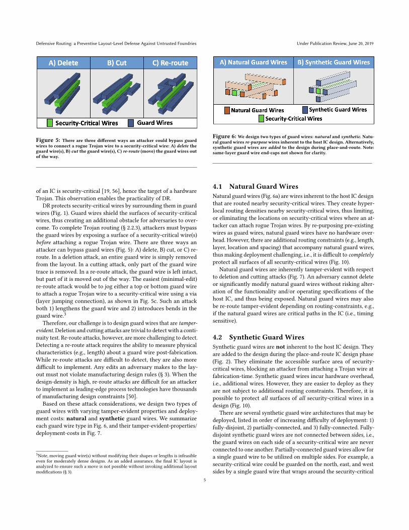
Figure 6: We design two types of guard wires: natural and synthetic. Natu-ral guard wires re-purpose wires inherent to the host IC design. Alternatively,synthetic guard wires are added to the design during place-and-route. Note:same-layer guard wire end-caps not shown for clarity.
4.1 Natural Guard WiresNatural guard wires (Fig. 6a) are wires inherent to the host IC designthat are routed nearby security-critical wires. They create hyper-local routing densities nearby security-critical wires, thus limiting,or eliminating the locations on security-critical wires where an at-tacker can attach rogue Trojan wires. By re-purposing pre-existingwires as guard wires, natural guard wires have no hardware over-head. However, there are additional routing constraints (e.g., length,layer, location and spacing) that accompany natural guard wires,thus making deployment challenging, i.e., it is difficult to completelyprotect all surfaces of all security-critical wires (Fig. 10).
Natural guard wires are inherently tamper-evident with respectto deletion and cutting attacks (Fig. 7). An adversary cannot deleteor significantly modify natural guard wires without risking alter-ation of the functionality and/or operating specifications of thehost IC, and thus being exposed. Natural guard wires may alsobe re-route tamper-evident depending on routing-constraints, e.g.,if the natural guard wires are critical paths in the IC (i.e., timingsensitive).
4.2 Synthetic Guard WiresSynthetic guard wires are not inherent to the host IC design. Theyare added to the design during the place-and-route IC design phase(Fig. 2). They eliminate the accessible surface area of security-critical wires, blocking an attacker from attaching a Trojan wire atfabrication-time. Synthetic guard wires incur hardware overhead,i.e., additional wires. However, they are easier to deploy as theyare not subject to additional routing constraints. Therefore, it ispossible to protect all surfaces of all security-critical wires in adesign (Fig. 10).
There are several synthetic guard wire architectures that may bedeployed, listed in order of increasing difficulty of deployment: 1)fully-disjoint, 2) partially-connected, and 3) fully-connected. Fully-disjoint synthetic guard wires are not connected between sides, i.e.,the guard wires on each side of a security-critical wire are neverconnected to one another. Partially-connected guard wires allow fora single guard wire to be utilized on multiple sides. For example, asecurity-critical wire could be guarded on the north, east, and westsides by a single guard wire that wraps around the security-critical
5

Under Publication Review, June 20, 2019 Timothy Trippel, Kang G. Shin, Kevin B. Bush, and Matthew Hicks
Figure 7: Natural guard wires require no hardware overhead, but have ad-ditional routing constraints governing their deployment. They are tamper-evident with respect to deletion and cutting attacks (Fig. 5). Synthetic guardwires require additional wires, but no additional routing constraints. Syn-thetic guard wires are tamper-evident with respect to all guard wires attacks(Fig. 5) using post-fabrication fault analysis techniques like continuity testsand TDR [12, 39, 53, 55].
wire. Lastly, fully-connected guard wires are formed when a singleguard wire is routed around all sides of all security-critical wires.
Unlike natural guard wires, synthetic guard wires are not inher-ently tamper-evident. To enable post-fabrication tamper analysis(§ 2.4 and 6.4), the analog characteristics of guard wire segmentsmust be observable. This can be implemented either on-chip, e.g.,with internal sensors [25] or ring oscillators [63], or off-chip, e.g.,with an I/O pin and a one-time programmable fabric [35].
5 IMPLEMENTATIONWe develop an automated tool-chain for deploying DR in modernIC designs. Our toolchain integrates with existing IC design flows(Fig. 2) that utilize commercial VLSI CAD tools. Specifically, weimplement the DR toolchain around the Cadence Innovus Imple-mentation System [11], a commercial place-and-route (PaR) CADtool. The tool-chain is invoked by modifying a place-and-route TCLscript,4 as shown in Fig. 8.
5.1 Place-&-Route ProcessThe PaR design phase (Fig. 2) is typically automated by a CAD tool,programmatically driven by TCL script(s). There are several steps toPaR that are performed in the following order: 1) floorplanning, 2)placement, 3) clock tree synthesis, 4) routing, and 5) filling. To ensurethat all guard-wires are routed optimally, we modify the order of thesePaR steps. Specifically, after floorplanning (1), we use our automatedtoolchain to place security critical components and route security-critical- and guard- wires. Our toolchain then permanently fixesthe locations of these components and wires to prevent the PaRCAD tool from modifying their positions and/or shapes throughoutthe remainder of the PaR process. Lastly, we utilize the PaR CADtool to place non-security-critical components (2), synthesize theclock tree (3), route non-security-critical (4) and fill the design withfiller (cap) cells.
5.2 Automated ToolchainThe DR toolchain automates the insertion of either natural or syn-thetic guard wires around security-critical wires. The toolchainconsists of three main phases (Fig. 8). The first phase (A) identifiessecurity-critical nets. The second phase (B) identifies the unblocked
4Tool Command Language (TCL) scripts are the standard programmatic interface tocommercial VLSI CAD tools. IC designers often develop a set of scripts for driving theCAD tools that automate most of the IC design process (Fig. 2).
Figure 8: DR is an automated toolchain consisting of three phases. Ourtoolchain first identifies which wires are security-critical, determines poten-tial (unblocked) attachment points, and routes guard wires to block all attach-ment points. Security-critical components & wires are placed & routed beforephase (A) of our toolchain is invoked. Before continuing with the traditionalPaR flow, the security-critical nets and their guard wires are locked in-placeto ensure they are untouched throughout the remainder of the layout process.
surfaces of all security-critical interconnect within a GDSII-encodedlayout. The last phase (C) guards the security-critical interconnectsby routing guard wires nearby. We provide additional implementa-tion details on all three stages of the DR toolchain below.
5.2.1 Identifying Security-Critical Nets. The first phase of DRrequires identifying those nets that are security-critical (i.e., wiresto guard). Like prior work [23, 35], we assume the designer hasannotated the HDL to flag nets that are to be treated as “security-critical” by appending a unique prefix to such signal names. 5 Fromhere, we perform a circuit-level dataflow analysis to generate signalfan-in graphs from the hand-annotated HDL. Specifically, our tooltakes as input a Verilog netlist and the (root signal) annotations,and returns a graph detailing the signal(s) that comprise the fan-into those root signals, to a configurable depth.
Given the interconnected nature of signals within an IC de-sign, an adversary may elect to target a wire that influences a rootsecurity-critical wire, rather than the root wire itself. To addressthis indirection, our tool widens the set of signals deemed “security-critical” beyond the scope of those (hand-annotated) root security-critical signals. Since the netlist is often modified by the PaR CADtool to meet various design constraints (e.g., power, performance,and area), we invoke our dataflow analysis after all security-criticalwires have first been routed (§ 5). Note: while CAD tools can op-timize (i.e., modify) the design netlist through the IC design flow,they leave signal name prefixes intact.
5.2.2 IdentifyingUnblockedWire Surfaces. The second phaseof DR identifying the unblocked surfaces of security-critical inter-connect in a physical IC layout, i.e. potential Trojanwire attachmentlocations. To do so, we use GDS2Score [37], an open-source frame-work for computing security metrics over an IC layout. GDS2Score
5Prior work [23, 35] makes the same assumption as security-critical signals are bestidentified at the HDL level, where there are additional design semantics. Additionalwork has also demonstrated ways of making such classifications at the HDL levelsemi-autonomously [19, 23, 62].
6

Defensive Routing: a Preventive Layout-Level Defense Against Untrusted Foundries Under Publication Review, June 20, 2019
Figure 9: Defensively routed OR1200 processor SoC with natural (A) andsynthetic (B) guard wires deployed around the privilege-bit signal wire (red).DR prevents an attacker from attaching a rouge wire to modify this signal.
takes as input a GSDII file (encoding an IC layout) and a security-critical signal graph (dataflow analysis output), and computes secu-rity metrics detailing the IC layout’s fabrication-time attack surface.GDS2Score provides three metrics: 1) net blockage, 2) trigger space,and 3) route distance. Specifically, the GDS2Score net blockagemetric reports the location of all security-critical wires within thelayout, and the surfaces of each security-critical wire that are un-blocked. By computing the net blockage metric immediately afterall security-critical wires are routed, GDS2Score provides exactlocations of where to route guard wires.
5.2.3 Guard Unblocked Wire Surfaces. The last stage of theDR toolchain (Fig. 8) is a custom guard wire routing tool. We im-plement this tool in Python. It takes as input exact locations ofsecurity-critical wires and their unblocked sides (output from theGDS2Score net blockage metric) and generates a TCL script thatintegrates with the Cadence Innovus Digital Implementation plat-form [11] to automatically route the guard wires. This TCL scriptis executed immediately after the security-critical wires have beenrouted, but before placing the remaining non-security critical com-ponents. Depending on the type of guard wires being deployed,natural, synthetic, or both, different guard wire TCL scripts aregenerated as described below.
Natural GuardWires. There are numerous ways natural guardwires can be implemented. Since commercial PaR CAD tools donot offer an interface to enable fine-grain constraints betweentwo unrelated signal wires, we develop an indirect method forimplementing natural guard wires. We implement natural guardwires by constraining placement and routing resources nearby
security-critical wires. First, we identify all circuit components (i.e.,logic gates) connected to all security-critical wires, i.e., security-critical components. Next, we draw a bounding box around thesecomponents and extend this boundary vertically by 10% of theoverall box height, and horizontally by 10% of the overall box width.Then, we set placement and routing density screens in the portionof the IC layout that lies outside the security-critical bounding box.These constraints limit the placement and routing resources outsidethe bounding box, thus forcing more components and wiring withinthe bounding box. With increased routing density nearby security-critical wires, they are less accessible by Trojan payload deliverywires. The density screen configuration settings are optimized tomaximize the net blockage metric computed by the GDS2Scoremetric. Fig. 9a depicts natural guard wires deployed around thesecurity-critical privilege bit signal of the OR1200 processor ICdesign.
SyntheticGuardWires. Synthetic guardwires aremore straight-forward to implement. The automated guard wire deploymenttoolchain locates all unblocked surfaces (north, south, east, west,top, and bottom) of all security-critical wires and routes guard wiresin these regions. After all guard wire segments are routed, theyare connected according to the architecture chosen (§ 4.2). Fig. 9bdepicts synthetic guard wires deployed around the security-criticalprivilege bit signal of the OR1200 processor IC design.
6 EVALUATIONWe evaluate DR in three areas. First, we explore the effectiveness ofDR at closing the fabrication-time attack surface of three security-critical IC designs of commercial complexity, comparing the capa-bilities of DR with state-of-the-art layout-level defenses [4, 5, 60].Next, we demonstrate the practicality of DR, analyzing its power,performance, and area overheads. Finally, we perform a threat as-sessment, demonstrating how guard wires are tamper-evident.
6.1 Experimental Setup6.1.1 IC Designs. We utilize three IC designs for our evaluation:OR1200 processor SoC, AES accelerator, and DSP accelerator. TheOR1200 processor SoC is an open-source design [42] used in previ-ous fabrication-time attack studies [61]. The AES and DSP accel-erator designs are open-sourced under the Common EvaluationPlatform (CEP) benchmark suite [36]. The OR1200 processor SoCconsists of a 5-stage pipelined OR1200 CPU that implements the 32-bit OR1K instruction set and Wishbone bus interface. It runs Linuxand busybox. The AES accelerator supports 128-bit key sizes. TheDSP accelerator implements a Fast Fourier Transform algorithm.
All designs target a 45nm Silicon-On-Insulator (SOI) processtechnology. They are synthesized with Cadence Genus (v16.23)and placed-and-routed using Cadence Innovus (v17.1). All designstarget a 100MHz clock frequency and a core density of 60–70%.All ICs are synthesized and placed-and-routed on a server with2.5GHz Intel Xeon E5-2640 CPU and 64 GB of memory runningRed Hat Enterprise Linux (v6.9).
6.1.2 Root Security-Critical Signals. Signals (nets) are classi-fied as security-critical if they are apart of the fan-in to a set ofroot security critical signals that are hand annotated by the HDLdesigner (§ 5.2.1). For the OR1200 processor design, we select the
7

Under Publication Review, June 20, 2019 Timothy Trippel, Kang G. Shin, Kevin B. Bush, and Matthew Hicks
supervisor signal (supv) as security critical, because altering this sig-nal enables an attacker to escalate the privilege mode of the entireprocessor, as shown in previous work [18, 26, 61]. For the AES accel-erator, we mark the 32-bit key-loading register as security-critical.Attacking the key-loading register of the AES accelerator enablesthe attacker to leak encryption keys. Lastly, for the DSP accelera-tor, we mark the the next_out signal as security-critical. The DSPaccelerator’s next_out signal indicates to external hardware whenan FFT computation is ready at the output registers. Tamperingwith the next_out signal allows the attacker to hide specific outputsof the chip. Fig. 12 (far right) shows the number of interconnectwires our automated toolchain classifies as security-critical, withthe aforementioned root signals marked as security-critical, foreach IC layout.
6.2 EffectivenessWe first evaluate the effectiveness of DR in thwarting the insertionof hardware Trojans at fabrication-time. We compare the degree ofprotection provided by DR with that provided by deploying anotherlayout-level defense suggested by Ba et al. [4, 5]. This placement-based defense involves filling as many empty component placementsites as possible (they show that filling 100% of placement sites isinfeasible), prioritizing empty sites nearest security-critical nets.Weuse our automated toolchain (§ 5.2) to deploy both types of guardwires (natural and synthetic). We simulate Ba et al.’s placementdefense [4, 5] using a custom GDS2Score extension.
6.2.1 GDS2Score. We use the open-source GDS2Score frame-work [37] to quantify the effectiveness of each defense. GDS2Scoreanalyzes the physical layout of an IC (encoded in a GSDII file) com-putes security metrics detailing the IC layout’s fabrication-timeattack surface.
GDS2Score provides three metrics: 1) net blockage, 2) triggerspace, and 3) route distance. Thenet blockagemetric computes thepercentage of surface area of security-critical nets that are blockedby other circuit components or wiring. The trigger space metriccomputes the amount of unused placement sites on the devicelayer that may be utilized by an adversary to place a Trojan triggeror payload circuit(s). Lastly, the route distance metric computesthe minimal distance between unblocked security-critical nets andunused placement sites that an adversary would have to route arogue Trojan wire to “connect” the hardware Trojan to the hostIC. The trigger space metric details the difficulty of performingTrojan placement, while the net blockage and route distance metricsdetail the difficulty of performing Trojan routing. Specifically, weuse GDS2Score’s net blockage and route distance security metricsto compare both types of DR guard wires and placement-centricdefenses across the three test IC designs.
6.2.2 Net Blockage Results. Both types of guard wires, natu-ral and synthetic, attempt to block security-critical interconnectwires to prevent attackers from attaching rogue wires to them,thus, minimizing/eliminating possible Trojan configurations, i.e.,(security-critical-wire, trigger-space6) pairs. We use GDS2Score’s
6“Trigger-spaces” are a GDS2Score term for contiguous open placement sites on thedevice layer.
AES DSP OR1200IC Design
0
20
40
60
80
100
Net
Blo
ckag
e (%
)
nonenaturalsynthetic
Figure 10: Plot of the GDS2Score net blockage metric computed acrossthree different IC layouts, with and without guard wires.
net blockage metric to compute the surface-area-coverage differ-ences between natural and synthetic guard wires. Fig. 10 comparesthe net blockage computed across 9 total IC layouts: three circuitdesigns with no guard wires, natural guard wires, and syntheticguard wires.
Across all three designs, synthetic guard wire provide moreprotection than natural guard wires. Specifically, for all 3 designs,synthentic guard wires achieve 100% net blockage. This means thatthere is no place on any security-critical net in these designs wherean attacker can attach a rogue wire. Natural guard wires are unableto achieve 100% coverage due mainly to having to meet their ownrouting constraints which prevents our tool from creating enoughnets to block an entire security-critical wire.
6.2.3 Route Distance Results. Since DR only limits the routingresources needed to insert a Trojan at fabrication time, it is vitalto understand how DR reduces the overall fabrication-time attacksurface, i.e., both Trojan routing and placement resources (triggerspaces). We use GDS2Score’s route distance metric to enumerate allpossible (security-critical-wire, trigger-space) pairs, i.e., all availableTrojan placement and routing resources an attacker can utilize toinsert a Trojan at fabrication time. Namely, we use GDS2Score’sroute distance metric to illustrate the attack surface of a given IClayout.
Fig. 11 shows the route distance metric as computed across threedifferent IC designs, with and without layout-level defenses includ-ing: 1) DR (both natural and synthetic guard wires) and 2) defensiveplacement. Each heatmap is intended to be analyzed column-wise,where each column is a histogram of the distances between un-blocked security-critical wires and trigger-spaces within a sizerange. Namely, each heatmap illustrates the fabrication-time attacksurface of each IC layout. If a circuit has no attack configurations,i.e., all security-critical wires are blocked or there are no trigger-spaces, the route distance heatmap is completely dark (columnratios of 0). If it is impossible to eradicate all attack configurations,the most secure layout for such a circuit would have maximumdistances between unblocked security-critical wires and trigger-spaces, i.e., a heatmap with the top row the lightest color (top rowratios of 1). This is because larger distances increase the signal delay
8

Defensive Routing: a Preventive Layout-Level Defense Against Untrusted Foundries Under Publication Review, June 20, 2019
Figure 11: Plot of the GDS2Score route distance metric computed across three different IC layouts, with and without guard wires and Ba et al.’s defensiveplacement [4, 5]. Each heatmap illustrates the percentage of (security-critical-wire, trigger-space) pairs (possible attack configurations) of varying distances apart.The heatmaps are intended to be analyzed by column, as each column encodes a histogram of possible attack configurations with trigger-spaces of a given sizerange (X-axis). Route distances (Y-axis) are displayed in terms of standard deviations frommeannet length in each respective design.Heatmaps that are completelydark indicate no possible attack configurations exist, i.e. no placement/routing resources to insert a Trojan.
for the hardware Trojan; increasing the challenge of the attackerto meet timing constraints for their attack.
Synthetic guardwires outperformnatural guardwires and placement-centric defenses. For all three IC designs, synthetic guard wireswere able to close the fabrication-time attack-surface by completelyblocking all security-critical wires (Fig. 10). Thus, DR demonstratesan effective layout-level defense.
6.3 PracticalityDR is effective, but is it practical? We evaluate the cost of deploy-ing DR across the three IC layouts. Specifically, we analyze thepower, route density, and performance (timing) overheads incurred
by deploying both natural and synthetic guard wires. While it iscommon to analyze power, performance, and area, of an IC layout,we instead analyze power, performance and route density. Areameasurements of a layout refer to the device-layer area, i.e., widthand length, since the height (number of routing layers) is fixed fora given process technology. Since DR does not require additionallogic gates, we do not increase the width and height (area) of thecore area, rather DR alters the total wire length in the design. Thus,measuring routing density overhead is more meaningful. We usethe built-in features of Cadence tools to compute these overheads.
Fig. 12 details our results. Power and timing overheads were bothless than 1%. In some cases, the timing was better for the guard wire
9

Under Publication Review, June 20, 2019 Timothy Trippel, Kang G. Shin, Kevin B. Bush, and Matthew Hicks
OR1200 DSP AESIC Design
05
101520253035
Pow
er (
mW
)
PowerNoneNaturalSynthetic
OR1200 DSP AESIC Design
0
20
40
60
80
100
Rout
e D
ensi
ty (
%)
Route DensityNoneNaturalSynthetic
OR1200 DSP AESIC Design
0.0
0.5
1.0
1.5
2.0
Tim
ing
Slac
k (n
s)
TimingNoneNaturalSynthetic
OR1200 DSP AESIC Design
100
101
102
103
# o
f Sec
urit
y-Cr
itic
al W
ires
53
5
1342
# of Security-Critical Wires
Figure 12: DR hardware overheads. The far right plot highlights the number of wires deemed security-critical in each design for context.
designs. This is expected as DR does not require any additional logicgates, nor lengthen existing wires. Rather, the guard wires increaserouting constraints that can push the PaR CAD tool to producemore optimal routing solutions. The route density overheadwas lessthan 1% for all natural guard wires, and similar for synthetic guardwires when the number of security-critical wires to guard is small,namely the OR1200 and DSP layout. Intuitively, the more guardwires inserted, the higher the routing density increase. Keepingroute density low is important to ensure automated CAD tools canroute each design. However, even though all layouts targeted aplacement density (density of logic gates on the device layer) of 60–70%, route density was relatively low even with guard wires. Thiswas due to the characteristics of the designs and process technology(i.e., back-end-of-line metal stack option).
6.4 Threat AnalysisLastly, we provide a threat analysis of DR. Recall (Fig. 5), thereare three ways an attacker could bypass guard wires to carry outa fabrication-time attack: A) delete a guard wire, B) cut a guardwire, or C) re-route a guard wire. The first two attacks, deletionand cutting, are trivial to detect (§ 4). The third attack, guard wirere-route, is the most sophisticated (Fig. 5c). Only synthetic guardwires can reliably detect such an attack using TDR (Fig. 7).
6.4.1 Smallest Re-route Attack. The minimum (re-route) attackedit an adversary canmake to a guard wire is to jog a top (or bottom)guard wire to an adjacent routing track, and attach to the security-critical wire from above (or below) with a via, as illustrated inFigure 5c. This edit is minimal because the the minimal metal pitch(MMP), or (horizontal) distance between the centers of adjacentrouting tracks on the same routing layer, is much smaller than the(vertical) distance between overlapping routing tracks on adjacentrouting layers. Specifically, the smallest (re-route) attack edit wouldincrease a guard wire’s length by: Lattack = 2 ∗ MMPr , whereMMPr is the MMP on layer, r , which is defined in the design rulesof a given process technology. Table 1 summarizes the minimal-length-edits to a synthetic guard wire an attacker must make tobypass DR, according to the 45nm process technology we target inthis study.
6.4.2 Tamper Detection with TDR. When IC interconnects areinjected with a pulsed waveform with a rise time less than twice thepropagation delay of the interconnect, they behave like transmis-sion lines (Eq. (1)). Hence, time-domain reflectometry (TDR) can beused to measure several characteristics of synthetic guard wires toensure they have not been tampered with (§ 2.4). Specifically, thelengths of each guard wire can be analyzed with TDR to detect ifthey have been altered. Once measured, the lengths can be com-pared with that predicted by a 3D electromagnetic field solver [33].While modeling all interconnects within a large complex IC usinga field solver is computationally impractical, it is practical to ana-lyze only a small subset of interconnects, e.g., the guard wires andsurrounding circuit structures [39].
Prior work demonstrates terahertz TDR systems [12, 39, 53, 55]capable of measuring the propagation delay of an interconnect toan accuracy of ±2.6 femptoseconds (f s). Such systems utilize laser-driven optoelectronic measurement techniques to achieve such highresolutions. According to the ideal transmission line model [52], thepropagation delay, Tpd , is a function of the dielectric constant, Dk ,speed of light, C , and length of the transmission line (guardwire), Lдw , as shown in Eq. (2).
Tpd = Lдw ∗√DkC
(2)
Table 1:Minimumguardwire re-route attack (Fig. 5) edit–distances for eachrouting layer in our target (IBM 45nm SOI) process technology.
Routing Min Wire Min Metal Min Attack TDR
Layer Spacing (um) Pitch (um) Edit (um) Detectable?
1 0.07 0.14 0.28 ✓
2 0.07 0.14 0.28 ✓
3 0.07 0.14 0.28 ✓
4 0.09 0.19 0.38 ✓
5 0.09 0.19 0.38 ✓
6 0.14 0.28 0.56 ✓
7 0.14 0.28 0.56 ✓
8 0.80 1.60 3.20 ✓
9 0.80 1.60 3.20 ✓
10 2.00 4.00 8.00 ✓
10

Defensive Routing: a Preventive Layout-Level Defense Against Untrusted Foundries Under Publication Review, June 20, 2019
106
107
108 Guard WiresUnmodifiedAttacked
1 2 3 4 5 6 7 8 9 10Routing Layer
100
101
G
uard
Wir
e Le
ngth
(um
)
Figure 13: Worst-case manufacturing process variation (error bars) effecton unmodified and minimal re-route attacks on 100-micron guard-wires.
6.4.3 Process Variation& TDRAccuracy. TDR is the ideal tam-per detection tool as process variation has no impact on its accuracy.Recall that knowing the inter-layer dielectric constant of the in-sulating material surrounding synthetic guard wires is all that isrequired to compute their lengths using TDR ( Eq. (2)). The dielec-tric constant of the inter-layer dielectric is not dependent on itsgeometric properties, thus the dielectric constant is usually verywell controlled [10].
6.4.4 Process Variation &GuardWire Lengths. Detecting theminimal guard-wire re-route attack requires detecting the smallestincrease to a guard wire’s length required to move it out of the way(§ 6.4.1). This distance is larger than the worst-case manufac-turing process variation in a guard wire’s length. Namely, withLattack as the minimum length guard wire (re-route) attack edit,Ldesiдn as the designed length of the guard wire, and Lwc_error ,as the worst-case manufacturing error in the actual guard wire’slength (+ or -):
Ldesiдn − Lwc_error + Lattack > Ldesiдn + Lwc_error (3)
For a guard wire on routing layer r , theworst-casemanufacturingerror, Lwc_error , can be deduced from the manufacturing designrules as:
Lwc_error = 2 ∗ min_spacinдr2
=min_spacinдr(4)
, wheremin_spacinдr is theminimum required spacing surroundinga wire routed on metal layer, r .
We illustrate this in Figure 13, where we plot theminimum lengthdifferences between unmodified (un-attacked) andminimally-rerouted(attacked) guard wires, overlaid with error bars indicating the worst-case range of variation in a guard wires fabricated length caused byprocess variation. Even in the worst case, across all routing layers,unmodified vs attacked guard wires are discernible.
6.4.5 TDR Simulation. Using the TDR propagation delay modeldescribed in Eq. 2, and the previously studied capabilities of opto-electrical terahertz TDR [12, 39, 53, 55], we simulate the differencein reflection times for single pulse TDR waveforms applied to syn-thetic guard wires of various lengths. Specifically we compare the
1 2 3 4 5 6 7 8 9 10Metal (Routing) Layer
0
5
10
15
20
25
# M
easu
rem
ents
Confidence Level95%99%
Figure 14: Number of TDR wire length measurements required to detectminimal re-route attacks (Tab. 1) with 95% and 99% confidence, per layer.
reflection time of an (unmodified) 100 micron long guard wire andcompare it to the reflection time observed from a similar guardwire that has been lengthened by the minimal attack edit distancefor each routing layer (Tab. 1). We assume a dielectric constant of3.9, the nominal dielectric constant of silicon dioxide [27]. Takinginto account a (Gaussian) standard error (across reflection timemeasurements) of ± 2.6 f s , as reported by [39], we compute theminimum number of TDR measurements required to discriminatean unmodified guard wire from an attacked guard wire with confi-dence levels of 95% and 99%. We plot these results in Figure 14. Ourresults demonstrate that existing terahertz TDR systems are capableof detecting the minimum re-route attacks across all routing layers(Tab. 1) in our target 45nm process, requiring at most 14 and 24TDR measurements to achieve confidence levels of 95% and 99%,respectively.
7 DISCUSSIONDR targets the prevention of fabrication-time attacks. Experimentswith IC layouts of three designs show that it is effective, deployable,and tamper-resistant. Provided below is additional discussion onits signal integrity impact, flexibility, scalability, and extensibility.
Signal Integrity Impact.Routing longwires parallel to security-critical wires increases coupling capacitance, thus creating cross-talk between the guard and security-critical wires. However, syn-thetic guard wires are not actively driven (and can be grounded)during normal chip operation. Thus, cross-talk is not an issue—infact, synthetic guard wires decrease cross-talk by acting as sheildsbetween security-critical signals and the rest of the circuit. Naturalguard wires, on the other hand, have the potential to cause signalintegrity and timing issues. These issues can be avoided by onlyusing wires with low switching rates as natural guard wires.
Defense-in-Depth. While DR alone is capable of thwartingeven the stealthiest fabrication-time attacks, its low deploymentcosts enable defense-in-depth. Layering DR with other preventivemeasures, such as Ba et al.’s defensive placement [4, 5], providesan additional layer of protection.
Scalability.Although Moore’s law is near at its limit, transistorscontinue to shrink. Only three companies are capable of manufac-turing 7–10nm transistors [31]. It is, therefore, vital for DR to scalewith process technology. With respect to deletion or cutting attacks
11

Under Publication Review, June 20, 2019 Timothy Trippel, Kang G. Shin, Kevin B. Bush, and Matthew Hicks
(Fig. 5), both natural and synthetic guard wires scale with processtechnology advancements as continuity checks are the only testsnecessary to detect tampering. With respect to re-route attacks,synthetic guard wires will scale, provided TDR capabilities con-tinue to scale. This is likely as advancements in microelectronicfeature sizes translate to advancements in the technologies builtupon them.
Extensibility of CAD Tools. Our DR deployment framework(§ 5) is built on top of a commercial IC CAD tool [11] and open-source VLSI analysis tools [37, 38]. Extending this framework towork across other commercial IC layout CAD tools involves incor-porating support for each vendor’s CAD tool APIs. We foresee DRdeployed as a deeply integrated component of commercial VLSICAD tools as they focus more on IC security.
8 RELATEDWORKFabrication-time attacks and defenses have been extensively studied.While most attacks have only been contrived in literature [9, 26, 28,34, 47, 61], a recent Bloomberg business week article [45] claims tohave discovered the first fabrication-time attack in the wild. Whilethis attack was done at the PCB level, prior studies primarily focuson the IC level, where components are much smaller and henceeasier to conceal. With respect to defenses, there have been manyproposed techniques [1, 2, 4, 5, 7, 15, 16, 24, 32, 40, 60, 64], butbesides DR, have all failed against the A2 Trojan [61].
Fabrication-time Attacks. Attacks have spanned the trade-space of footprint size, stealth, and controllability. Specifically,some attacks have demonstrated stealth and controllability, at thecost of large footprints [9, 26, 34], while others have demonstratedsmall (or non-existent) footprints, at the cost of controllability andstealth [28, 47]. The most formidable attack in particular—the A2attack [61] —has demonstrated all three: small footprint, stealth,and controllability.
The first fabrication-time insertion of a hardware Trojan wasdeveloped by Lin et al. [34] who proposed a Trojan designed to leakinformation over a deliberately created side channel. Specifically,they designed and implemented a hardware Trojan, with a footprintof approximately 100 logic gates, to create an artificial power sidechannel for leaking cryptographic keys. Albeit unique at the time,today such a large footprint makes the attack detectable via sidechannel defenses [2, 7, 16].
Dopant level [9, 47] Trojans explore how altering the IC fabri-cation process in a targeted way can produce ICs with transistorsthat wear out quickly, causing the circuit to fail early. These Tro-jans demonstrate a fabrication-time attack where no additionalcircuit components need to be added, thus being extremely stealthy.However, dopant-level Trojans have several drawbacks. First, theyhave limited capabilities as they can only be constructed out ofcomponents already in the target IC design. Second, dopant levelalterations are detectable with optical microscopy [51].
The most lethal fabrication-time attack is the A2 Trojan, devel-oped by Yang et al. [61]. The A2 Trojan utilizes analog componentsto build a counter-based trigger circuit with a footprint of less thanthe size of one flip-flop. Its complex triggering mechanism makes itstealthy, i.e., unlikely to accidentally deploy during post-fabrication
functional testing or under normal chip operation, yet is control-lable from user-level software. Its unique design makes it the onlyTrojan to evade all detection schemes, except DR.
Fabrication-time Defenses. There are two fabrication-timeattack defense strategies: detective or preventive. Most prior workhas focused on detective strategies, while few works have focusedon preventive strategies. Detective strategies involve side-channelanalysis [2, 7, 24, 40], imaging [1, 64], and on-chip sensors [16, 32].Until DR, preventive measures been placement-focused [4, 5, 60].We highlight both detective and preventive defenses below.
The first side-channel detection schemewas proposed byAgrawalet al. [2]. They used power, temperature, and electromagnetic (EM)side-channel measurements to record a fingerprint of a “golden”IC during normal, and compared this fingerprint to one acquiredfrom an untrusted IC. Similarly, Jin et al. [24] create a timing-basedfingerprint obtained by measuring the output delays resulting fromapplying various input combinations to a given IC. While side-channel detection schemes are effective against hardware Trojanswith large footprints, they fail at detecting Trojans like A2 [61],whose side-channel signatures are well below operational noisemargins.
Like side-channel detection, imaging is another detective defense.Specifically, backside imaging is a non-destructive technique thatcan resolve device-layer components (Fig. 3) as this layer isn’tblocked by any wires. Zhou et al. [64] propose filling the placementgrid with highly reflective fill cells, as opposed to the standardfill cells used, to encode a watermark that can be captured usingbackside imaging. Thus, if thewatermark has been perturbed duringfabrication, an attack has occurred. Unfortunately, this techniquerequires hours to image a single IC, provides no visibility in metallayers, and its resolution seems capped at 45 nm processes.
9 CONCLUSIONDR is the first routing-centric preventive defense against fabrication-time attacks. It makes attaching Trojan logic to security-criticallogic in the victim IC infeasible by routing guard wires on all sixsides of security-critical wires, eliminating locations where an ad-versary can attach rogue Trojan wires. DR guard wires are tamperevident, indicating if a foundry-level attacker modified them toinsert a hardware Trojan. We design and implement two guardwire variants: natural and synthetic. The former consists of wiresinherent to the host IC layout, that are vital to the functionalityof the design, but not security-critical. The latter are not inherentto the functionality of the design, and are added during the place-and-route IC design phase. Both guard wire variants are capable ofdetecting deletion and cutting attacks. Using terahertz time-domainreflectometry (TDR), synthetic guard wires can also detect re-routeattacks (Fig. 5) across all routing layers of our 45nm process.
We develope an automated framework for deploying both naturaland synthetic guard wires. We evaluate the effectiveness, deploya-bility, and tamper-resistance of DR across three different IC designsincluding a processor SoC, AES and DSP accelerators. The exper-imental results show that DR thwarts the insertion of even thestealthiest known additive hardware Trojans, across all 3 layouts,with power, timing, and area overheads of less than 1%.
12

Defensive Routing: a Preventive Layout-Level Defense Against Untrusted Foundries Under Publication Review, June 20, 2019
ACKNOWLEDGMENTSWe thank Brian Tyrrell, Matt Guyton, and other members of theMIT Lincoln Laboratory community for their thoughtful feedbackthat enhanced the quality of our work.
DISTRIBUTION STATEMENT A. Approved for public release.Distribution is unlimited. This material is based upon work sup-ported under Air Force Contract No. FA8702-15-D-0001. Any opin-ions, findings, conclusions or recommendations expressed in thismaterial are those of the author(s) and do not necessarily reflectthe views of the U.S. Air Force.
This material is based upon work supported by the NationalScience Foundation Graduate Research Fellowship Program underGrant No. DGE 1256260. Any opinions, findings, and conclusionsor recommendations expressed in this material are those of theauthor(s) and do not necessarily reflect the views of the NationalScience Foundation.
REFERENCES[1] Ronen Adato, Aydan Uyar, Mahmoud Zangeneh, Boyou Zhou, Ajay Joshi, Bennett
Goldberg, and M Selim Unlu. 2016. Rapid mapping of digital integrated circuitlogic gates via multi-spectral backside imaging. arXiv:1605.09306 (2016).
[2] Dakshi Agrawal, Selcuk Baktir, Deniz Karakoyunlu, Pankaj Rohatgi, and BerkSunar. 2007. Trojan Detection using IC fingerprinting. In IEEE Symposium onSecurity and Privacy (SP).
[3] Yousra Alkabani and Farinaz Koushanfar. 2008. DesignerâĂŹs hardware Trojanhorse. In IEEE International Workshop on Hardware-Oriented Security and Trust(HOST).
[4] Papa-Sidy Ba, Sophie Dupuis, Manikandan Palanichamy, Giorgio Di Natale, BrunoRouzeyre, et al. 2016. Hardware Trust through Layout Filling: a Hardware TrojanPrevention Technique. In IEEE Computer Society Annual Symposium on VLSI(ISVLSI).
[5] Papa-Sidy Ba, Manikandan Palanichamy, Sophie Dupuis, Marie-Lise Flottes,Giorgio Di Natale, and Bruno Rouzeyre. 2015. Hardware Trojan preventionusing layout-level design approach. In European Conference on Circuit Theoryand Design (ECCTD).
[6] Halil B Bakoglu. 1990. Circuits, Interconnections, and Packaging for VLSI. (1990).[7] Josep Balasch, Benedikt Gierlichs, and Ingrid Verbauwhede. 2015. Electromag-
netic circuit fingerprints for hardware trojan detection. In IEEE InternationalSymposium on Electromagnetic Compatibility (EMC).
[8] Mark Beaumont, Bradley Hopkins, and Tristan Newby. 2011. Hardware trojans-prevention, detection, countermeasures (a literature review). Technical Report.Defence Science and Technology Organization Edinburgh (Australia).
[9] Georg T Becker, Francesco Regazzoni, Christof Paar, and Wayne P Burleson.2013. Stealthy dopant-level hardware trojans. In International Workshop onCryptographic Hardware and Embedded Systems (CHES).
[10] Duane Boning and Sani Nassif. 2000. Models of process variations in device andinterconnect. Design of high performance microprocessor circuits (2000).
[11] Cadence Design Systems. [n. d.]. Innovus Implementation System. ([n. d.]).https://www.cadence.com/content/cadence-www/global/en_US/home.html.
[12] Yongming Cai, Zhiyong Wang, Rajen Dias, and Deepak Goyal. 2010. ElectroOptical Terahertz Pulse ReflectometryâĂŤan innovative fault isolation tool. InElectronic Components and Technology Conference (ECTC), 2010 Proceedings 60th.
[13] Rajat Subhra Chakraborty, Seetharam Narasimhan, and Swarup Bhunia. 2009.Hardware Trojan: Threats and emerging solutions. In IEEE International HighLevel Design Validation and Test Workshop (HLDVT). IEEE.
[14] Ming-Kun Chen, Cheng-Chi Tai, and Yu-Jung Huang. 2006. Nondestructiveanalysis of interconnection in two-die BGA using TDR. IEEE Transactions onInstrumentation and Measurement (2006).
[15] Ronald P Cocchi, James P Baukus, Lap Wai Chow, and Bryan J Wang. 2014.Circuit camouflage integration for hardware IP protection. In Proceedings of the51st Annual Design Automation Conference. ACM, 1–5.
[16] Domenic Forte, Chongxi Bao, and Ankur Srivastava. 2013. Temperature tracking:An innovative run-time approach for hardware Trojan detection. In IEEE/ACMInternational Conference on Computer-Aided Design (ICCAD).
[17] Leonard A Hayden and Vijai K Tripathi. 1994. Characterization and model-ing of multiple line interconnections from time domain measurements. IEEETransactions on Microwave Theory and Techniques (1994).
[18] Matthew Hicks, Murph Finnicum, Samuel T. King, Milo M. K. Martin, andJonathan M. Smith. 2010. Overcoming an Untrusted Computing Base: Detectingand Removing Malicious Hardware Automatically. In Proceedings of the IEEE
Symposium on Security and Privacy (SP).[19] Matthew Hicks, Cynthia Sturton, Samuel T. King, and Jonathan M. Smith. 2015.
SPECS: A Lightweight RuntimeMechanism for Protecting Software from Security-Critical Processor Bugs. In International Conference on Architectural Support forProgramming Languages and Operating Systems (ASPLOS).
[20] Simon Hollis and SimonWMoore. 2006. RasP: an area-efficient, on-chip network.In 2006 International Conference on Computer Design. IEEE, 63–69.
[21] Simon J Hollis. 2009. Pulse generation for on-chip data transmission. In 200912th Euromicro Conference on Digital System Design, Architectures, Methods andTools. IEEE, 303–310.
[22] Ching-Wen Hsue and Te-Wen Pan. 1997. Reconstruction of nonuniform trans-mission lines from time-domain reflectometry. IEEE Transactions on MicrowaveTheory and Techniques (1997).
[23] Yier Jin, Nathan Kupp, and Yiorgos Makris. 2010. DFTT: Design for Trojan test.In IEEE International Conference on Electronics, Circuits, and Systems (ICECS).
[24] Yier Jin and Yiorgos Makris. 2008. Hardware Trojan detection using path delayfingerprint. In IEEE International Workshop on Hardware-Oriented Security andTrust (HOST).
[25] Shane Kelly, Xuehui Zhang, Mohammed Tehranipoor, and Andrew Ferraiuolo.2015. Detecting hardware trojans using on-chip sensors in an ASIC design.Journal of Electronic Testing 31, 1 (2015), 11–26.
[26] Samuel T. King, Joseph Tucek, Anthony Cozzie, Chris Grier, Weihang Jiang, andYuanyuan Zhou. 2008. Designing and Implementing Malicious Hardware. InProceedings of the Usenix Workshop on Large-Scale Exploits and Emergent Threats(LEET).
[27] Angus I Kingon, Jon-Paul Maria, and SK Streiffer. 2000. Alternative dielectrics tosilicon dioxide for memory and logic devices. Nature (2000).
[28] Raghavan Kumar, Philipp Jovanovic, Wayne Burleson, and Ilia Polian. 2014.Parametric trojans for fault-injection attacks on cryptographic hardware. InWorkshop on Fault Diagnosis and Tolerance in Cryptography (FDTC).
[29] Mark Lapedus. 2017. Battling Fab Cycle Times. (February 2017). https://semiengineering.com/battling-fab-cycle-times/.
[30] Mark Lapedus. 2018. Big Trouble At 3nm. (June 2018). https://semiengineering.com/big-trouble-at-3nm/.
[31] Mark Lapedus. 2018. GF Puts 7nm On Hold. (August 2018). https://semiengineering.com/gf-puts-7nm-on-hold/.
[32] Jie Li and John Lach. 2008. At-speed delay characterization for IC authenticationand Trojan horse detection. In IEEE International Workshop on Hardware-OrientedSecurity and Trust (HOST).
[33] Jun Jun Lim, Nor Adila Johari, Subhash C Rustagi, and Narain D Arora. 2014.Characterization of Interconnect Process Variation in CMOS Using ElectricalMeasurements and Field Solver. IEEE Transactions on Electron Devices (2014).
[34] Lang Lin, Markus Kasper, Tim Güneysu, Christof Paar, andWayne Burleson. 2009.Trojan Side-Channels: Lightweight Hardware Trojans through Side-Channel En-gineering.. In International Workshop on Cryptographic Hardware and EmbeddedSystems (CHES).
[35] Timothy Linscott, Pete Ehrett, Valeria Bertacco, and Todd Austin. 2018. SWAN:mitigating hardware trojans with design ambiguity. In 2018 IEEE/ACM Interna-tional Conference on Computer-Aided Design (ICCAD). IEEE, 1–7.
[36] MIT Lincoln Laboratory. [n. d.]. Common Evaluation Platform. ([n. d.]). https://github.com/mit-ll/CEP.
[37] MIT Lincoln Laboratory. [n. d.]. GDS2-Score. ([n. d.]). https://github.com/mit-ll/gds2-score.
[38] MIT Lincoln Laboratory. [n. d.]. Nemo. ([n. d.]). https://github.com/mit-ll/nemo.[39] Michael Nagel, Alexander Michalski, and Heinrich Kurz. 2011. Contact-free fault
location and imaging with on-chip terahertz time-domain reflectometry. OpticsExpress (2011).
[40] Seetharam Narasimhan, Xinmu Wang, Dongdong Du, Rajat Subhra Chakraborty,and Swarup Bhunia. 2011. TeSR: A robust temporal self-referencing approachfor hardware Trojan detection. In IEEE International Symposium on Hardware-Oriented Security and Trust (HOST).
[41] C Odegard and C Lambert. 1999. Comparative TDR analysis as a packaging FAtool. In ISTFA 1999: 25 th International Symposium for Testing and Failure Analysis.
[42] OpenCores.org. [n. d.]. OpenRISC OR1200 Processor. ([n. d.]). https://github.com/openrisc/or1200.
[43] Dan L Philen, Ian AWhite, Jane F Kuhl, and Stephen CMettler. 1982. Single-modefiber OTDR: Experiment and theory. IEEE Transactions on Microwave Theory andTechniques (1982).
[44] Miodrag Potkonjak, Ani Nahapetian, Michael Nelson, and Tammara Massey.2009. Hardware Trojan horse detection using gate-level characterization. InProceedings of ACM/IEEE Design Automation Conference (DAC).
[45] Jordan Robertson and Michael Riley. 2018. The Big Hack: HowChina Used a Tiny Chip to Infiltrate U.S. Companies. (Oct 2018).https://www.bloomberg.com/news/features/2018-10-04/the-big-hack-how-china-used-a-tiny-chip-to-infiltrate-america-s-top-companies.
[46] Masoud Rostami, Farinaz Koushanfar, Jeyavijayan Rajendran, and Ramesh Karri.2013. Hardware Security: Threat Models and Metrics. In Proceedings of theInternational Conference on Computer-Aided Design (ICCD).
13

Under Publication Review, June 20, 2019 Timothy Trippel, Kang G. Shin, Kevin B. Bush, and Matthew Hicks
[47] Yuriy Shiyanovskii, F Wolff, Aravind Rajendran, C Papachristou, D Weyer, andW Clay. 2010. Process reliability based trojans through NBTI and HCI effects. InNASA/ESA Conference on Adaptive Hardware and Systems (AHS).
[48] D Smolyansky. 2004. Electronic Package Fault Isolation Using TDR. ASM Inter-national (2004).
[49] PI Somlo and DL Hollway. 1969. Microwave Locating Reflectometer. ElectronicsLetters (1969).
[50] Ed Sperling. 2018. Design Rule Complexity Rising. (April 2018). https://semiengineering.com/design-rule-complexity-rising/.
[51] Takeshi Sugawara, Daisuke Suzuki, Ryoichi Fujii, Shigeaki Tawa, Ryohei Hori,Mitsuru Shiozaki, and Takeshi Fujino. 2014. Reversing stealthy dopant-levelcircuits. In International Workshop on Cryptographic Hardware and EmbeddedSystems (CHES).
[52] James Sutherland. 1999. As Edge speeds increase, wires become transmissionlines. EDN (1999).
[53] MY Tay, L Cao, M Venkata, L Tran, W Donna, W Qiu, J Alton, PF Taday, andM Lin. 2012. Advanced fault isolation technique using electro-optical terahertzpulse reflectometry. In Physical and Failure Analysis of Integrated Circuits (IPFA),2012 19th IEEE International Symposium on the.
[54] Mohammad Tehranipoor and Farinaz Koushanfar. 2010. A survey of hardwaretrojan taxonomy and detection. IEEE Design & Test of Computers 27, 1 (2010).
[55] TeraView. [n. d.]. Electro Optical Terahertz Pulse Reflectometry: The worldâĂŹsfastest and most accurate fault isolation system.
[56] Mohit Tiwari, Hassan M.G. Wassel, Bita Mazloom, Shashidhar Mysore, Frederic T.Chong, and Timothy Sherwood. 2009. Complete Information Flow Tracking fromthe Gates Up. In International Conference on Architectural Support for ProgrammingLanguages and Operating Systems (ASPLOS). 109–120.
[57] TSMC. 2019. TSMC Fabrication Schedule âĂŤ 2019. (April 2019). https://www.mosis.com/db/pubf/fsched?ORG=TSMC.
[58] Adam Waksman, Matthew Suozzo, and Simha Sethumadhavan. 2013. FANCI:identification of stealthy malicious logic using boolean functional analysis. InProceedings of the ACM SIGSAC Conference on Computer & CommunicationsSecurity (CCS).
[59] Francis Wolff, Chris Papachristou, Swarup Bhunia, and Rajat S Chakraborty.2008. Towards Trojan-free trusted ICs: Problem analysis and detection scheme.In Proceedings of the ACM Conference on Design, Automation and Test in Europe(DATE).
[60] Kan Xiao and Mohammed Tehranipoor. 2013. BISA: Built-in self-authenticationfor preventing hardware Trojan insertion. In IEEE International Symposium onHardware-Oriented Security and Trust (HOST).
[61] Kaiyuan Yang, Matthew Hicks, Qing Dong, Todd Austin, and Dennis Sylvester.2016. A2: Analog malicious hardware. In IEEE Symposium on Security and Privacy(SP).
[62] Rui Zhang, Natalie Stanley, Christopher Griggs, AndrewChi, and Cynthia Sturton.2017. Identifying Security Critical Properties for the Dynamic Verification of aProcessor. In International Conference on Architectural Support for ProgrammingLanguages and Operating Systems (ASPLOS).
[63] Xuehui Zhang and Mohammad Tehranipoor. 2011. RON: An on-chip ring oscilla-tor network for hardware Trojan detection. In 2011 Design, Automation & Test inEurope. IEEE, 1–6.
[64] Boyou Zhou, Ronen Adato, Mahmoud Zangeneh, Tianyu Yang, Aydan Uyar,Bennett Goldberg, Selim Unlu, and Ajay Joshi. 2015. Detecting hardware tro-jans using backside optical imaging of embedded watermarks. In Proceedings ofACM/EDAC/IEEE Design Automation Conference (DAC).
14