Embed Size (px)
Citation preview

LUND UNIVERSITY
PO Box 117221 00 Lund+46 46-222 00 00
DC Distributed Power Systems - Analysis, Design and Control for a Renewable EnergySystem
Karlsson, Per
2002
Link to publication
Citation for published version (APA):Karlsson, P. (2002). DC Distributed Power Systems - Analysis, Design and Control for a Renewable EnergySystem. IEA-LTH, Box 118, SE-221 00 LUND, SWEDEN,.
Total number of authors:1
General rightsUnless other specific re-use rights are stated the following general rights apply:Copyright and moral rights for the publications made accessible in the public portal are retained by the authorsand/or other copyright owners and it is a condition of accessing publications that users recognise and abide by thelegal requirements associated with these rights. • Users may download and print one copy of any publication from the public portal for the purpose of private studyor research. • You may not further distribute the material or use it for any profit-making activity or commercial gain • You may freely distribute the URL identifying the publication in the public portal
Read more about Creative commons licenses: https://creativecommons.org/licenses/Take down policyIf you believe that this document breaches copyright please contact us providing details, and we will removeaccess to the work immediately and investigate your claim.

DC Distributed Power Systems
Analysis, Design and Control for a
Renewable Energy System
Per Karlsson
Doctoral Dissertation in Industrial Electrical Engineering
Department of Industrial Electrical Engineering and Automation

ii
Department of Industrial Electrical Engineering and Automation Lund University Box 118 SE-221 00 LUND SWEDEN
ISBN 91-88934-25-X CODEN:LUTEDX/(TEIE-1033)/1-200/(2002)
© 2002 Per Karlsson Printed in Sweden by Media-Tryck, Lund University Lund 2002

iii
Abstract
Renewable energy systems are likely to become wide spread in the future due to environmental demands. As a consequence of the dispersed nature of renewable energy systems, this implies that there will be a distributed generation of electric power. Since most of the distributed electrical energy sources do not provide their electric power at line frequency and voltage, a DC bus is a useful common connection for several such sources. Due to the differences in output voltage among the sources, depending on both the type of source and their actual operating point, the sources are connected to the DC power system via power electronic converters. The intention behind the presented work is not to replace the existing AC power system, but to include local DC power systems. The AC and DC power systems are connected at some points in the network. The renewable energy sources are weak compared to the present hydro power and nuclear power plants, resulting in a need of power conditioning before the renewable energy is fed to the transmission lines. The benefit of such an approach is that power conditioning is applied on a central level, i.e. at the interface between the AC and DC power systems.
The thesis starts with an overview of related work. Present DC transmission systems are discussed and investigated in simulations. Then, different methods for load sharing and voltage control are discussed. Especially, the voltage droop control scheme is examined thoroughly. Since the droop control method does not require any high-speed communication between sources and loads, this is considered the most suitable for DC distributed power systems. The voltage feed back design of the controller also results in a specification of the DC bus capacitors (equivalents to DC link capacitors of single converters) needed for filtering. If the converters in the DC distribution system are equipped with capacitors selected from this design criterion and if the DC bus impedance is neglected, the source converters share the total load equally in per unit.

iv
The same DC distribution bus configuration is studied in a wind power application. Especially the dynamic properties of load-source interactions are highlighted. They are interesting since the sources are considered weak for a distributed power system. This is illustrated with simulations where the power is fed from wind turbines only and constant power loads are controlled at the same time as the DC bus voltage level. The wind power generators are modeled as permanent-magnet synchronous machines. The controller needed for the machines, including position estimation and field weakening, is discussed. To control the DC bus voltage, the available wind power must be higher than the power consumed by the loads and the excess power removed by pitch angle control. Pitch angle control is a comparably slow process and, therefore, the DC bus voltage controller must handle the transient power distribution.
Personal safety and prevention of property damage are important factors of conventional AC power systems. For the investigated DC power system this is maybe even more important due to the fact that the star point of the sources and loads is left ungrounded or grounded through high impedance. The difficulty of detecting ground faults arises from the fact that the AC sources and loads are ungrounded or have high impedance to ground in order to effectively block zero-sequence currents flowing between the AC systems. A grounding scheme for the DC distribution system together with algorithms for detection of ground faults, are presented. The proposed method detects ground faults on both the AC and DC sides and is extended to cover short circuit faults with a minor work effort.
Two schemes for high voltage interconnection of DC systems are studied. One of them provides galvanic isolation, which is an advantage since elevated voltage might appear in the DC systems otherwise, in the case of a ground fault in the high voltage interconnection.
Experimental verifications follow the theoretical investigations introduced above. First, dynamic properties are studied and the behaviour predicted from theoretical analysis and simulations is verified. Then, load sharing is investigated. Also in this investigation, the experimental results agree with the simulated.

v
Acknowledgements
First, I would like to thank my colleague and friend Jörgen Svensson who I have worked with the last three years. I would also like to express my sincere gratitude to my friend and former colleague Martin Bojrup, who I worked with during 1996-1999.
I am very grateful to my two mentors, Professor Lars Gertmar and Professor Sture Lindahl. Both Lars and Sture have time to discuss all kinds of topics, not only technical.
I would also like to thank my supervisors, Professor Mats Alaküla and Professor Gustaf Olsson. Professor Alaküla, who has been my main supervisor, has shown much enthusiasm for power electronics, not strictly focusing on the research project. Even if his schedule is tight, Mats has always time to give a helping hand. Mats has also encouraged me to participate in courses and meetings, which is greatly acknowledged. Gustaf is also head of the department. As such, he strives hard to provide a friendly atmosphere at the department, which has been very successful.
The steering committee, including the four professors above, and Dr Magnus Akke, Dr Olof Samuelsson and Dr Jan Svensson has contributed with valuable comments and discussions. This has enhanced my work and is greatly acknowledged.
I would also like to thank Anders Lasson, ABB Utilities AB, and Ulf Thorén, Sydkraft AB from the steering committee of the former research project I was involved in together with Martin Bojrup.
Professor Frede Blaabjerg and Dr Stig Munk Nielsen, both at Aalborg University in Denmark, have also meant a lot to me. In 1996 they assisted me when I evaluated the SABER simulation software. Professor Blaabjerg also evaluated my Licentiate’s thesis on Quasi Resonant DC Link Converters.

vi
I would like to express my gratitude to the staff at IEA. Even if all the people at the department are helpful and friendly there are those that I owe a special thank. Dr Christian Rosen is a very good friend and a person you can discuss anything with. He has also proof read several of my articles, which is greatly acknowledged. Also at IEA, Getachew Darge and Bengt Simonsson have provided practical help for electronic designs. I think that Bengt has at least one catalogue or data book for every apparatus and component. I must thank Dr Ulf Jeppsson who used to maintain the UNIX-system with softwares like SABER and ACE, and nowadays takes care of the economical issues of the department. Thanks to the former Associate Professor at IEA, Stig Lindquist, for always being nice.
I am very thankful to Magnus, Mats, Lars, Christian, Jan and Jörgen for proof reading my thesis.
I have also had the privilege to work together with Annika Nilsson, Department of Building and Environmental Technology, Lund University. Annika does not hesitate to teach environmental issues in an advanced course on power electronics or present the same material on a conference on power electronics.
I also thank the staff at ABB University in Ludvika, especially Ewa Wikström and Elly Hartings, for encouraging me to participate in their courses on HVDC and HVDC Light.
I do not know how to thank my family enough. My parents, Siv and Axel, have always encouraged me to study without putting any requirements on the result. They have also helped me with all kinds of practical issues and financial support for my undergraduate studies. I cannot imagine that this would have been possible without your help – thanks again. My dear and beloved Anna has enhanced my life to a large extent. Though I spend too much time at the department, Anna does not complain. I hope that I sometime can return this patience when she needs it.
The Control of Renewable Energy Sources (CORE) project is financially supported by DESS (Delegationen för Energiförsörjning i SydSverige, The Board for Energy Supply in Southern Sweden). This support is gratefully acknowledged.
Per Karlsson

vii
Contents
CHAPTER 1 INTRODUCTION ...........................................................1
1.1 Objectives .......................................................................................... 2
1.2 Contributions .................................................................................... 3
1.3 Outline of the thesis........................................................................... 4
1.4 Publications ....................................................................................... 5
1.5 Previous work .................................................................................... 7
1.6 Specification of a distributed power system...................................... 20
CHAPTER 2 EXISTING DC POWER SYSTEMS................................21
2.1 HVDC ............................................................................................ 22
2.2 VSC based HVDC .......................................................................... 26
CHAPTER 3 DC BUS VOLTAGE CONTROL....................................31
3.1 Investigated system .......................................................................... 32
3.2 DC bus model ................................................................................. 33
3.3 Controller structure ......................................................................... 34
3.4 Cable impedance ............................................................................. 44
3.5 Load sharing .................................................................................... 56
3.6 Concluding remarks ........................................................................ 61
CHAPTER 4 WIND POWERED DC BUS ..........................................63
4.1 Pitch angle control........................................................................... 64
4.2 Droop offset control ........................................................................ 66
4.3 Speed estimation.............................................................................. 67
4.4 Field weakening ............................................................................... 68
4.5 Simulations...................................................................................... 70

viii
CHAPTER 5 FAULT DETECTION AND CLEARANCE ....................79
5.1 Grounding and fusing...................................................................... 79
5.2 Fault situations ................................................................................ 80
5.3 Detection and selectivity .................................................................. 88
5.4 Simulations...................................................................................... 94
CHAPTER 6 DC TRANSMISSION...................................................105
6.1 The back-to-back structure ............................................................ 105
6.2 The DAB structure ........................................................................ 109
6.3 Proposed interconnection structure ............................................... 114
CHAPTER 7 MEASUREMENTS .......................................................119
7.1 Experimental set-up ....................................................................... 119
7.2 Dynamic properties ....................................................................... 121
7.3 Load sharing .................................................................................. 130
CHAPTER 8 CONCLUSIONS ..........................................................135
8.1 Summary of results ........................................................................ 135
8.2 Future work ................................................................................... 138
REFERENCES ....................................................................................139
APPENDIX A MODULATION .........................................................149
A.1 Modulation methods ..................................................................... 149
A.2 Vector representation..................................................................... 155
APPENDIX B VECTOR CONTROL.................................................167
APPENDIX C CONVERTER LOSSES...............................................171
APPENDIX D NORMALISATION ...................................................177
D.1 Base system for a single converter................................................... 177
D.2 Converter data expressed in per unit .............................................. 178
APPENDIX E NOMENCLATURE ....................................................183

1
Chapter 1
Introduction
In this chapter DC distributed power systems (DPS) are introduced together with a review of the DC DPS state of the art technology. Renewable energy systems are likely to become wide spread in the future, due to environmental demands, for example, regarding pollution. This implies that there will be a distributed generation of electric power. Since several of the distributed electrical energy sources provide DC voltage, several such sources might be connected. Due to the differences in output voltage among the sources, depending on both the type of source and their actual operating point, the sources are connected to the DC power system via power electronic converters.
It should be clear that the intention is not to replace the existing AC power system, but to include local DC systems [14]. These AC and DC systems are connected at some points in the network. The benefit of such an approach arises from the fact that renewable energy sources are weak compared to present fossil fuel, hydro power and nuclear power plants, resulting in a need of power conditioning before being fed to the transmission lines. With a DC distributed system, conditioning can be applied at a central level of the AC distribution system, close to the DC system connection points. Also, several consumer loads operate on DC (rectified AC). Therefore, DC distribution could be used to omit the need for transformers and rectifiers in every single load.
The DC distributed power system has various kinds of energy storage added, which means that it can support nearby customers during AC power system failure or emergency situations. Also, sensitive equipment likely to be installed in future intelligent buildings also needs energy backup, i.e. uninterruptable

2 Chapter 1. Introduction
power supply (UPS) properties. This is already in use, for example, in telecommunication sub-stations where backup batteries are usually installed. Another example is given in [63] where a battery powered DC system is supplying the AC system circuit breaker control system. Of course, reliable operation of such systems is necessary.
A larger part of the power transmission network is likely to use high voltage direct current (HVDC) transmission technology in the future [14]. Also, the recently introduced medium voltage DC (MVDC) technology is likely to be used in DC distributed power systems [14]. This implies that future electric power systems constitute a mixture between AC and DC technology.
A distributed power system with as much as several hundred power electronic converters, call for new methods and technologies, both on the operator and system level. Not only an increased control effort is required, but also the complexity of protection systems will increase in the case of dispersed generation [31]. This is true especially if autonomous operation of the distributed power system is intended.
This work addresses control and stability issues of DC distributed power systems together with their connections to surrounding AC power systems, sources and loads. Also grounding and issues on fault detection and clearance are considered.
1.1 Objectives
The main objective of this work is to study the consequences of large-scale incorporation of power electronic converters in DC distributed power systems. The main objective is split into several sub-objectives, all imperative for a large-scale system. The first issue to treat is selection of a suitable system voltage, at least at the consumer level. Stability and dynamic properties of DC voltage control are of great concern. Requirements on hardware and software should be stated so that the system could grow, i.e. additional converters installed in an existing system, without system degradation. Voltage control in the case of weak sources should also be investigated, since several of the renewable energy sources possess low inertia. Suitable grounding and fault detection schemes should be investigated. Connection of several DC systems should be investigated. One important objective is that the need of communication should be studied.

1.2 Contributions 3
1.2 Contributions
The contributions of this work are given in Chapters 3 to 7 and concluded in Chapter 8. The main results are summarised here. Suitable voltage levels are not explicitly discussed in the thesis. Instead, a DC bus voltage level suitable for 400 V AC sources and loads is adopted. This is due to the fact that by doing so, the proposed system voltage covers existing consumer loads. Future apparatus might require a different load voltage level. To compensate this shortcoming, a large portion of the investigation is made on a per unit (p.u.) basis. Therefore, the results can be used for any DC bus voltage level.
The converters are first specified with focus on interaction between the AC and DC sides. Then a DC bus voltage droop controller is adopted. The demands on interaction together with droop requirements give a specification of the relation between rated power and converter DC side filter, i.e. DC bus capacitance, for each converter. The dynamic properties are investigated, both by means of stability analysis, in terms of root-locus, and large-signal simulations. It is found that for reasonable DC bus cable parameters, stability is of minor concern, for the selected DC side filter. In other words, the requirements on interaction between input and output of the converters is stronger than the stability requirement. Voltage droop control provides autonomous load sharing, implying that communication is not needed. The selected implementation of the droop algorithm and the controller parameters allow an arbitrary number of converters in the DC system. Furthermore, the already inserted units are not altered if additional units are incorporated.
A wind powered DC system is adopted to investigate voltage control and load sharing in the case of renewable energy sources. In this case a speed droop algorithm is developed. The dynamic properties of speed and voltage droop control are investigated. It is concluded that low-speed communication is beneficial for non-dispatchable sources. A fault detection algorithm is developed. The algorithm is studied for different levels of communication, ranging from none to point-to-point communication. An existing converter topology is adopted for interconnection of DC systems. The same converter topology is also used for power transmission. Voltage droop control is adopted also here. Thus, high-speed communication is not necessary. However, when low-bandwidth communication is utilised, the system operator has the ability to control power flow. A laboratory set-up is designed to verify voltage control, load sharing and fault detection.
4 Chapter 1. Introduction
1.3 Outline of the thesis
This chapter contains a brief introduction to the thesis and the academic work presented. A survey of previous work is also given. Chapter 2 reviews classical HVDC and Voltage Source Converter (VSC) based HVDC transmission systems. The study includes simulations, where especially the harmonic content of the currents is compared.
In Chapter 3, voltage and power control methods for the investigated distributed power system are developed. This analysis also results in a method for selection of DC bus filter capacitors. The steady state and dynamic properties of the selected control scheme are investigated for varying cable parameters. Load sharing is investigated for different voltage control methods.
In Chapter 4, the same system but with weak sources is investigated. Here, the DC power system is fed only with wind power and still constant power loads can be supplied and the DC bus voltage controlled. Personal safety and protection of equipment are important issues for any power system and Chapter 5 is devoted to these topics. The chapter starts with a presentation of the grounding scheme and typical fault conditions. Then the methods of fault detection and localisation are presented and verified in simulations.
In Chapter 6, connection of DC distributed systems is considered. The proposed scheme contains a transformer, providing galvanic separation between different DC systems. In Chapter 7, measurement results verifying dynamic properties, load sharing and fault detection are presented. The work is concluded in Chapter 8.
MATLABTM Power System Blockset is utilised for the time-domain simulations of Chapter 2 where thyristor based converters are considered. DYMOLATM is utilised for the time-domain simulations including transistor based converters, i.e. for the simulation of VSC based HVDC transmission in Chapter 2 and all time-domain simulations in Chapters 3 to 7. Large-signal converter models are used for simulations investigating two-converter systems and DC transmission systems. Average converter models are utilised for simulations where load sharing or fault detection is investigated. Discrete-time controllers are utilised for both the large-signal and the average converter models. MATLABTM is used in Chapter 3 for investigation of stability for different cable parameters in terms of root-locus of the poles. The simulations in the appendixes are all carried out in MATLABTM-SIMULINKTM.

1.4 Publications 5
1.4 Publications
The results presented in this thesis regard DC bus voltage control and fault detection and clearance, found in Chapters 3, 4, 5 and 7. The main results of these chapters are also presented in
P. Karlsson and J. Svensson, "DC Bus Voltage Control for Renewable Energy Distributed Power Systems", IASTED Power and Energy Systems Conference, PES 2002 Conf. Proc., Marina del Rey, CA, USA, May 13-15, 2002, pp. 333-338.
P. Karlsson and J. Svensson, "Fault Detection and Clearance in DC Distributed Power Systems", IEEE Nordic Workshop on Power and Industrial Electronics, NORPIE 2002 workshop proc., Stockholm, Sweden, Aug. 12-14, 2002, CD-ROM pages 6.
P. Karlsson and J. Svensson, "DC Bus Voltage Control for a Distributed Power System", provisionally accepted for publication in IEEE transactions on power electronics, paper no. 2001-834-LP.
P. Karlsson and J. Svensson, "Voltage Control and Load Sharing in DC Distribution Systems", submitted to European Conference on Power Electronics and Applications, EPE 2003, Toulouse, France, Sept. 2-4, 2003.
The thesis author has also authored the publication
J. Svensson and P. Karlsson, "Wind Farm Control Software Structure", International Workshop on Transmission Networks for Offshore Wind Farms, workshop proc., Stockholm, Sweden, Apr. 11-12, 2002, proceeding pages 15.
in the same research project. The contribution made by the thesis author in the last paper is minor.
The previous work on off-board battery chargers for electric vehicles, also part of the research work, is reported in
P. Karlsson, M. Bojrup, M. Alaküla and L. Gertmar, "Efficiency of Off-Board, High Power, Electric Vehicle Battery Chargers with Active Power Line Conditioning Capabilities", European Conference on Power Electronics and Applications, EPE ‘97 Conf. Rec., Trondheim, Norway, Sept. 8-10, 1997, vol. 4, pp. 4688-4692.

6 Chapter 1. Introduction
M. Bojrup, P. Karlsson, B. Simonsson and M. Alaküla, "A Dual Purpose Battery Charger for Electric Vehicles", IEEE Power Electronics Specialists Conference, PESC ‘98 Conf. Rec., Fukuoka, Japan, May 17-22, 1998, vol. 1, pp. 565-570.
M. Bojrup, P. Karlsson, M. Alaküla and L. Gertmar, "A Multiple Rotating Integrator Controller for Active Filters", European Conference on Power Electronics and Applications, EPE ‘99 Conf. Rec., Lausanne, Switzerland, Sept. 7-9, 1999, CD-ROM pages 9.
P. Karlsson, M. Bojrup, M. Alaküla and L. Gertmar, "Zero Voltage Switching Converters", IEEE Nordic Workshop on Power and Industrial Electronics, NORPIE 2000 workshop proc., Aalborg, Denmark, Jun. 13-16, 2000, pp. 84-88.
P. Karlsson, M. Bojrup, M. Alaküla and L. Gertmar, "Design and Implementation of a Quasi-Resonant DC Link Converter", European Conference on Power Electronics and Applications, EPE 2001 Conf. Rec., Graz, Austria, Aug. 27-29, 2001, CD-ROM pages 10.
Only minor parts of the work reported in the second and third publications above are attributed the author of this thesis. The work on resonant converters reported in the other publications above is also the basis of the Licentiate’s thesis
P. Karlsson, "Quasi Resonant DC Link Converters - Analysis and Design for a Battery Charger Application", Licentiate thesis, Department of Industrial Electrical Engineering and Automation, Lund Institute of Technology, Lund, Sweden, November 1999.
This work was evaluated by Professor Frede Blaabjerg at the Department of Energy Technology, Aalborg University, Denmark.
Besides the publications within the research projects, another publication related to power electronics education has been presented
A. Nilsson, P. Karlsson and L. Gertmar, "Environmental Engineering in the Power Electronics Education", European Conference on Power Electronics and Applications, EPE 2001 Conf. Rec., Graz, Austria, Aug. 27-29, 2001, CD-ROM pages 10.
Less than half of the work of this paper is attributed the thesis author.

1.5 Previous work 7
1.5 Previous work
This section provides a literature survey of previous work on renewable energy sources and distributed power systems in which the most relevant previous work is discussed. A classification of the papers is made based on the nature of the references even though several of them cover more than one topic. However, the references are sorted under the topic, which the thesis author find most interesting in the context of the rest of the thesis.
Distributed energy systems
Several arguments for distributed power systems are listed in [31]. Among these, transmission capability saturation of centralised power systems and related stability problems seem most important. The additional intelligence needed to control, protect and maintain distributed power systems is focused in [31]. The future market of (DC) distributed power systems is discussed in [33], where it is concluded that the growing market includes computer, military/aerospace and communication applications. It is also stated that distributed power systems are more costly than centralised. Note that in [31], the distributed system is part of a nation wide power transmission/distribution system including dispersed generation. In [33], the distributed system intended is restricted to supply power to electronic equipment like inside a single computer.
Power electronics for use in renewable energy applications are discussed in [14]. Also some benefits and drawbacks associated with renewable energy sources are discussed. Photovoltaic, fuel cell and wind energy systems are reviewed briefly. Small-scale hydro pump stations or battery banks for electric energy storage are, however, not discussed in [14]. Still, they are included in the principal scheme of a distributed power system, together with flywheel and superconducting magnetic energy storages.
DC distributed power systems
Some of the literature studied does not fit into the study, though interesting. For example, [39][40][41][42][66] investigate a high current, low voltage DC mesh with thyristor based converters. In [39][40][42], a superconducting power system is considered, whereas an industrial power distribution system with inherent UPS properties is considered in [41][66]. The intended system

8 Chapter 1. Introduction
might contain several hundred thyristor based sources (rectifiers) and loads (inverters), but the simulated systems are of considerably lower complexity. In [39], a DC power system formed by one rectifier and three inverters is studied. In [40][41][42][66], three rectifiers are used as sources. Since three sources are present, load sharing has to be considered. In all these cases, DC voltage droop control is used to give appropriate load sharing. This means that a voltage droop characteristic is assigned to each source. In [40][66], the LVDC mesh is simplified to a ring bus and in [42] a superconducting energy storage (SMES) is added to the system. The paper [41] focuses on investigation of the droop scheme. It is stated that this works well for superconducting networks. However, the performance of a non-superconducting network is questioned.
In the literature the term power electronic building block (PEBB) is sometimes used as a term for generic building blocks for power conversion, control and distribution with control intelligence and autonomy. The work presented in [11] proposes a distributed digital controller for PEBBs. The main requirements and desired features of such a controller is discussed in [11]. The proposed controller is based on components presently available and used in other applications.
A 600 W front-end source converter module and a 300 W load converter module are designed in [36]. The source converter is designed for zero voltage transition (ZVT) technique and the load converter utilises zero voltage switching (ZVS) technique. The source converter is formed by a single-phase rectifier, equipped with a power factor corrector (PFC), i.e. followed by a boost converter. The DC system voltage equals 48 V. Experimental results are included in [36]. In [46], converter topologies suitable for DC distributed power systems are evaluated. Especially, source side front-end boost rectifier candidates are investigated but also load side converter modules.
Voltage control and load sharing
There are basically two different methods to achieve load sharing. One of the methods is referred to as the droop concept and the other as the master/slave concept.
For the droop concept, a finite loop gain for the DC voltage controller is adopted. A droop characteristic is obtained from the transfer function slope in the P-V plane at the desired DC bus voltage. Since this droop characteristic appears as a negative slope in the P-V plane, load sharing is obtained. The

1.5 Previous work 9
quality of load sharing is determined by the negative slope of the droop characteristic, i.e. for a steep slope, load sharing is good but voltage regulation is poor. On the other hand, for a shallow slope, load sharing is poor but voltage regulation is good. Therefore, a trade-off between voltage regulation and load sharing has to be made for the droop concept.
In the master/slave concept, only one of the source converters is controlling the DC bus voltage. The other source converters are current controlled. This results in a stiff DC bus voltage regulation and a fully controllable load sharing.
The papers [38][52][58] give an overview of these paralleling methods. According to [52], five different droop schemes exist. The first is based on the use of converters with inherent droop feature. The second scheme is based on voltage droop due to series resistors. The third scheme is called voltage droop via output current feedback. The fourth scheme is referred to as current mode with low DC gain. The fifth is scheduling control via a non-linear gain. The benefits of the droop schemes are the ease of implementation and expansion and that no communication between the converters (i.e. supervisory control) is needed. This gives high modularity and reliability. The main disadvantages are that the voltage regulation is degraded to achieve the droop characteristic and that the current sharing is poor due to open loop control of the entire system.
The next large group identified in [52] is referred to as active current sharing schemes. Common to these schemes, is that an additional control loop is used to provide current sharing. According to [52], three different active current sharing control structures are used for parallel converter systems. The first control structure is called inner loop regulation (ILR). The second control structure is referred to as outer loop regulation (OLR). The third structure relies on an external controller (EC). EC implies a large number of interconnections between the converters. This means that both the modularity and reliability might be degraded. It is, however, stated in [52] that the rapid development of distributed power systems implies that this technique should be examined in a new light. The high level supervisory controller can be redundant, and the converter cells are only responsible for gating and fault indication. This method is likely to yield the highest performance because of its possibility of interleaving [52].
Also six current programming (CP) methods for active current sharing schemes are reviewed in [52]. Of these six, three are average and three are

10 Chapter 1. Introduction
master/slave current programming methods. Seven methods to operate multiple DC-DC converters in parallel are given in [38]. In [58], four methods to achieve load sharing in parallel converter systems are given.
In [29], load sharing properties are studied by examining the output plane (output current versus voltage). A small-signal model is developed for the investigation. Simulations and experiments verify the theoretical results. The output plane is derived from equations for current programmed converters in [13]. The output plane is verified in large-signal simulations and experiments. Droop load sharing is evaluated in [37]. One of the important conclusions made in [37] is that the droop method requires precise control of the initial output voltage. It is also stated that the main advantages of the droop control method compared to other converter paralleling schemes, are the ease of implementation and that communication by means of control-wire connection is not required.
A droop function with a programmed droop resistance equal to the equivalent series resistance (ESR) of the output capacitor is proposed in [16]. Load sharing with the selected droop function is investigated by means of simulations and experiments.
A paralleling scheme called central-limit control, closely related to master/slave control, is presented in [64] and reviewed in [58]. The main difference between master/slave and central-limit control is that for the latter all the sources regulate the load converter DC bus voltage.
Autonomous master/slave current sharing is used in [62] for two source converters connected in parallel. A small-signal model for the two source converters together with their controllers is derived. A current sharing algorithm is also presented. Current sharing control is necessary since otherwise small differences in the source converter parameters would cause severe load imbalance. Also, the voltage loop is investigated. Design of the compensators is discussed but only a few actual results are concluded.
In a situation where several converters connected to the DC distribution bus that all control the voltage precisely to the reference at their respective connection point, load sharing among sources is not controlled. Instead, load sharing is entirely determined by the distribution bus impedance [75].
In [76], it is stated that distributed power systems have better performance than centralised. Moreover, it is stated that the sources connected in parallel to the DC bus (front-end boost rectifiers), should share the load to ensure proper

1.5 Previous work 11
operation. In [76], the droop method is used together with gain scheduling, which is said to give a robust design in terms of source-load interaction, i.e. good load sharing and good voltage regulation for a modular design approach.
According to [76], the main problems of master/slave load sharing are that fast communication is required and that a single point failure can disable the entire system. Also, all modules are control dependent. Six important issues are addressed in [76]. The first is stability, for example, in terms of interactions between parallel converters (especially in the case of three-phase sources due to the appearance of zero-sequence currents). The second important issue is load sharing when several sources are connected in parallel to the DC distribution bus. The third issue is modularity, i.e. the ability to manufacture and maintain the DC system. The fourth issue is autonomous control enhancing modularity and providing increased system reliability and redundancy. The fifth issue is DC bus voltage control, which is imperative. The sixth and last issue identified in [76], is the source output impedance which indeed affect several of the other issues, for example, the interaction between converters connected to the DC system.
The gain-scheduling method utilised in [76] is based on a modified droop method where the voltage loop gain is increased for increasing output power in such a way that the voltage error decreases compared to the case with a constant gain droop function. According to [76], both DC bus voltage control and load sharing show better performance compared to master/slave control. An interesting option not discussed in [76] is to use an adaptive controller for the DC bus voltage control.
In [44], a droop load sharing scheme is investigated where the DC bus voltage reference is adaptively controlled for each converter, in order to improve voltage regulation and load sharing.
Small-signal stability based on impedance specification
A system with an arbitrary number of DC-DC source converters paralleled using master/slave control, is investigated in [61]. Small-signal stability and dynamic performance are investigated. Also, a current sharing compensator is developed. The compensator is designed in the frequency-domain and verified through time-domain simulations.
A small-signal model for a parallel rectifier system is derived in [12]. Dynamic properties in the case of long inductive and resistive cables are investigated. It

12 Chapter 1. Introduction
is found that the cable parameters do not affect the dynamic properties extensively. Load sharing is investigated for both droop and master/slave methods. It is found that a system with parallel rectifiers is stable provided that each individual rectifier is stable when the droop method is applied. This is not true in the case of master/slave control, which should be designed carefully.
Small-signal stability criteria for DC-DC converter systems often end up in an impedance specification, where the relation between source converter output impedance Zo and total load converter input impedance Zi is given by
( )∑=<<k
kiio ZZZ ,11 (1.1)
where Zi,k is the input impedance for converter k. This impedance criterion was first established in the paper “Input Filter Considerations in Design and Application of Switching Regulators” written by Middlebrook in 1976 [55].
Some of the more recent impedance specifications for stable operation of DC distribution systems instead specify a “forbidden” region in the complex frequency plane [20][21][28][70]. In [70], a forbidden region for the total loop gain is specified so that a minimum phase margin is ensured. This is further developed in [20][21] where the individual load converter impedance is specified so that the forbidden region is avoided by applying
source
kload
ki
o
P
P
Z
Z ,
, 2
1Re ⋅−<
(1.2)
and
( ) kkiok ZZ Φ+°<∠−∠<Φ−°− 9090 , (1.3)
where
source
kload
o
kik P
P
Z
Z ,,
2
1arcsin ⋅⋅=Φ (1.4)
The results obtained in [20][21] are applied for the power supply of a Pentium processor in [71]. The power system of the investigated PC provides the voltage levels 3.3 V, 5 V and 12 V. The interactions between source and

1.5 Previous work 13
load are found to be strong but no instability occurs. However, it is found that conditional stability problems might occur. It is stated that conditional stability problems cannot be solved by the application of the impedance criterion. According to [71], there are two possible solutions to check for conditional stability. The first is to derive the system transfer function with different loads, which is generally very complicated. The second is to include gain information in the impedance criterion, giving a set of impedance curves for the source converter output impedance. There are also two methods reducing the risk for occurrence of conditional stability. The first is to increase the source converter DC side capacitance. The second is to apply a current feedback loop. The work in [20][21] together with the stability margin monitoring method presented in [22][23][24][50] is concluded in [25].
In the paper [65], the relationship between stability and DC bus capacitance is studied. Also fault propagation is investigated. The main objective of the investigation is to minimise the DC bus capacitance.
In [28], large DC power systems for space applications are investigated. Here, equation (1.1) is used for small-signal stability analysis. It is also pointed out that large-signal or transient stability issues are of great concern. The methods suggested for large-signal analysis are computer analysis involving Bode plots, Nyquist curves and transient responses. Also, hardware testing, both for validation and model development, are used in the stability analysis.
Input filter design is discussed in [27]. Here, all the DC-DC converters are equipped with an input filter. Initially, the effect of the input filter on the DC-DC converter transfer function is investigated. Then, the extra element theorem [56] is used to investigate the effect caused by the impedance seen from the filter input terminals. This impedance is divided into two parts: the source (series) impedance and the cumulative (shunt) impedance, i.e. the collective regulator input impedance resulting from the input filters of the other power modules. If
ds
ns
ZZ
ZZ
<<
<< (1.5)
hold, where Zs is the filter output impedance, Zn and Zd are the DC-DC converter input impedances with the output nulled and shorted, respectively, then the DC-DC converter transfer function is in principle unaltered by the input filter [27]. Furthermore, this means that the negative impedance

14 Chapter 1. Introduction
resulting from a constant power load is decoupled from the DC distribution bus. It is found that if several DC-DC converters, equipped with filters designed from this rule are connected to a common DC distribution bus, then the cumulative impedance is positive and decrease as the number of power modules increase. This means that the stability margin increases as the number of connected power modules increases.
In [51], power buffering is utilised to enhance stability of a DC distributed power system during transients. This is achieved by reducing the loop gain, and consequently, the negative incremental input impedance of the converters so that the sum of the source output impedance and the negative incremental input impedance is positive. This yields a stable system. Another possibility is also discussed in [51], where the power buffer is controlled to a certain input impedance during the transients.
Large-signal stability
Large-signal stability is treated in [2], where the distributed power system is formed by one single DC source with several load converters connected. Each load converter is equipped with an input LC-filter. The LC-filters are modeled as ideal except for a resistor R connected in series with the inductor. The large-signal stability constraints are expressed as boundaries on R. The upper limit for R is formed by application of the equilibrium point condition, i.e. by investigation of the maximum R yielding an intersection between the source and the load characteristics. According to [2], this gives
o
dc
P
VR
2
4
1 ⋅< (1.6)
where Vdc is the DC source voltage and Po is the load converter output power. The lower limit for R is found from the mixed potential criterion. In [2], lower limits on R are established for the cases with one, two and n load converters connected to a single DC source. However, computational problems appear for larger systems. Therefore, approximations are used in the case of multiple constant power loads. In the case of n constant power loads it is also assumed that these are equal in terms of filter component values and output power. For this case, an approximate lower bound is given by [2]
nnC
LR −> 22 (1.7)

1.5 Previous work 15
For high n, the resistance R has to be high, which implies high power dissipation. In [2], it is found that the approximation of the lower bound for R gives an error between the approximated maximum singular value and the exact approaching 11% as n increases.
Robustness against parameter uncertainty
In [47], DC power system stability is investigated with focus on robustness against parameter uncertainty. Robust control theories are applied to DC power systems. According to [47], this is done to cope with the sensitivity to parameter and load variation resulting in DC power systems prone to instability. The stability robustness is investigated by computing the multivariable stability margin, km, and the structured singular value, µ. Calculating these quantities exactly is cumbersome. Therefore, different approximation methods are investigated in [47].
The inherent instability of DC distribution systems originates from the fact that constant power loads appear as negative resistances to the regulators (source converters). The equivalent resistance seen from the regulator is [47]
P
v
i
vR bus
eq
2
−=∂∂= (1.8)
In [47], Middlebrook’s Criterion [55] is regarded as the normal way to handle this problem, i.e. to use an isolation concept. Two problems arise from using Middlebrook’s Criterion according to [47]. Firstly, parameter variations are not covered by the criterion and, secondly, it is intended for a two-port system. For the multiloop case considered in [47], a multiple input multiple output (MIMO) system should instead be investigated, which is not covered by Middlebrook’s Criterion. In [47], expressing the electrical system as a MIMO system and then use the convex hull algorithm to calculate the stability margin is instead emphasised. This method is compared to other.
Converter modeling and control
Modeling and control issues for front-end three-phase boost rectifiers are discussed in [34]. An average model is developed and the stability with different loads connected across the DC side is investigated. Since an average model is used, a constant power load is modeled as a resistor with negative resistance. A non-linear controller, e.g. with feed forward of the load current, gives the best performance.

16 Chapter 1. Introduction
Modeling of a four-leg inverter, i.e. a neutral connected inverter, used in a PEBB based DC distributed power system, is investigated in [67]. The four-leg converter is presented in [78]. As in [34], the converter model in [67] is averaged. The converter input filter is of LC-type but with an RC-circuit connected across the capacitor to increase the shunt impedance at high frequencies. The impedance overlap between the filter input and output impedances is investigated, to fulfil equation (1.1). As expected, the interaction between input and output decreases as the damper resistance increases, i.e. the phase margin increases. In [67], a single source converter formed by a transistor front-end rectifier is considered. The DC side filter of the transistor rectifier is formed by a capacitor. Interaction between the rectifier output filter and the inverter input filter is also investigated. As in the previous case, the phase margin increases with increasing damper resistance. The same result is achieved by increasing the rectifier DC side capacitance. A more interesting solution exists according to [67]: if the controller bandwidth is reduced, the phase margin is increased. The interesting characteristic about this feature is that it can be tuned online, whereas the system has to be shut down for the other two methods.
In [75], two source converters connected to the same DC distribution bus are modeled simultaneously to investigate their interaction. Here, master/slave control is used and it is claimed that the same control strategy as in the single source case applies. However, it is stated that for long distribution distances with several sources and loads, other control strategies are probably required.
A switch model for large-signal modeling of distributed power systems is studied in [10]. It is found that the simulation with the proposed model shows good agreement with device level simulations. It is also found that the simulation time is reduced significantly.
The zero-sequence current in distributed power systems
The fact that grid connected converters might give rise to high common mode currents is well known. This causes problems like bearing currents and insulation problems in electrical machines [48]. The common mode current results from the variations in voltage potential of the DC side supply rails, depending on the actual switch state. Consequently, the fundamental of the common mode current appears at switching frequency. The capacitive coupling between the supply rails and ground provides a path for the common mode current. Due to the capacitive nature of the current path, the common mode current magnitude increases with increasing switching frequency.

1.5 Previous work 17
In [72], the supply rail voltage shift is analysed. First, the neutral to ground voltage variation for a diode rectifier/three-phase converter combination is investigated. The neutral is in this case the star-point of the load at the converter output, which for example could be the star-point of an electrical machine. It is shown that the neutral to ground voltage varies as the negative supply rail to neutral voltage for the rectifier with the converter switching superimposed. Both simulations and measurements are shown. Second, the same investigation is made for a controlled rectifier/converter combination, connected back-to-back. In this case the situation is even worse, at least in terms of high frequency content, since the negative supply rail to ground voltage variation is determined by the switching frequency of the rectifier. According to [72], one way to partly reduce the problem is to synchronise the modulation carriers of the rectifier and converter. Note that synchronisation should be avoided if modularity and autonomous control is desired. Also a third case is investigated, where two generators feed the same DC distribution bus via transistor rectifiers. In this case it is complicated to synchronise the switching patterns since it is likely that the generators operate at different load conditions. Furthermore, there might be extremely high zero-sequence currents if both generators are grounded to the same physical ground potential. Three methods are proposed to reduce the problems related with common mode currents. First the alleviation method, which includes installing electromagnetic interference (EMI) suppressing chokes, filtering and the use of soft-switching techniques. The second method is referred to as a tolerant method, where EMI currents are allowed but shielding is used in the motor to reduce the bearing currents and insulation stress. The third method addresses new converter topologies, where the four-leg VSC [67][78] is mentioned as an example. In [1], high impedance grounding is investigated to manage problems associated with neutral voltage shift.
In [74], two transistor rectifiers are connected to the same generator (or equivalently AC power system) and the rectifiers feed the same DC distribution bus. It is found that in the average simulation model, in dq-coordinates (Appendix B), the zero-sequence current does not appear. Instead, a dq0 simulation model has to be adopted. In this simulation model, a high zero-sequence current appears. This problem is especially obvious when one of the rectifiers has the switch state 000 and the other 111 (Appendix A), which means that the DC distribution bus voltage is applied across the sum of the generator stator inductances for each phase. In [74], this is solved by adopting a modulation strategy where the zero voltage vectors, 000 and 111, are not utilised for the source rectifiers. In [77], a non-isolated system of one front–

18 Chapter 1. Introduction
end boost rectifier and one inverter is studied, from a converter modulation point of view. It is found that the proposed modulation scheme (interleaving) reduces the common mode current. In [75], ground loop interactions between two generators with a common ground, is also discussed.
An active filter for the DC bus is discussed in [73]. The active filter is formed by a transistor half-bridge and a DC link capacitor. The DC distribution bus side filter is purely inductive. The active filter is required to reduce AC current components injected from three-phase voltage source converters. These AC components result from negative-sequence or harmonic currents on the AC side of the three-phase converters. In [73], the switching frequency of the active filter is selected considerably higher than the one of the other converters of the DC distribution bus. The high switching frequency implies that interactions between the other converters can be suppressed, resulting in a stabilising effect. Consequently, the DC distribution bus impedance is tuned for best performance, thus, enhancing the stability. Note that the DC link capacitor voltage must be higher than the DC bus voltage, for the active filter.
Electromagnetic interference
In the paper [8], EMI problems related to switch mode power supplies connected to a DC distribution bus of long length are investigated. The load converter switching appears as a variable load, which generates reflections. The high rise and fall times generate high frequency signals radiated by the long power system conductors.
In [15], high frequency interaction in terms of disturbance propagation from DC distribution bus voltage to load converter output voltage is addressed. The problem is investigated from an analytical point of view and with simulations and experiments. The key result is that the switching frequencies of the converters should be as equal as possible to reduce load converter output oscillations.
Load flow and short circuit calculations
DC power system analysis in terms of load flow and short circuit calculations is investigated in [26]. Numerous source models (i.e. battery charger, rectifier and generator models) are given. Also connector models for load flow and short circuit calculations are investigated. Loads and branches are modeled. According to [26], the present standards (in the year 1996) are not complete and need further work.

1.5 Previous work 19
In [3], the methods of the IEC draft standard “Calculation of short circuit-currents in dc auxiliary installations in power plants and substations” are investigated. The calculations are intended to determine appropriate fusing for the system. Four different loads are investigated in [3]. These are the (thyristor) converter in 50 or 60 Hz AC systems, stationary lead-acid batteries, smoothing capacitors and DC motors. The straightforward methods given in the standard are compared with EMTP simulations. The standard gives conservative estimates of the short circuit currents (25% overestimated). Also, the time constants estimated according to the standard are longer than the simulated. The standard was not applicable (in the year 1996) to large DC systems, such as railway traction systems, HVDC transmission systems and photovoltaic systems. According to [3], the reason is that the models developed for the standard do not cover the set of electrical parameters appearing for these systems.
A detailed model of an RL-fed bridge converter for use in a Newton-Raphson power flow program for industrial AC/DC power systems is derived in [68]. This is done since bridge models in simulation packages are generally only valid in, for example, HVDC applications where the commutation resistance is negligible. Two systems are simulated to demonstrate the accuracy, a coal mine electrical power system and a railway power system. It is found that the developed model yields a considerably higher accuracy for systems with high commutation resistance.
Due to the differences between load-flow studies of AC and DC power systems, a new algorithm and a DC simulation package are developed in [79]. The load flow algorithm is based on the Newton–Raphson method. DC load flow simulation models are developed for constant DC voltage power sources, batteries, AC/DC rectifiers, constant power load, constant current load, constant resistance load and time-varying load. Several case studies are simulated, and their voltage profiles are shown.
Grounding
According to [72], the best ground point is the mid-potential between the positive and negative conductors of the DC distribution bus. This means that the voltage shift is localised to each sub-system. In [17], grounding issues for drive systems in general are discussed. A thorough analysis is presented and it is found that high impedance grounding is expected to be used in the future as fault detection systems become more accurate and reliable.

20 Chapter 1. Introduction
1.6 Specification of a distributed power system
This section contains the main requirements put on a future DC distributed power system. The requirements are based on the previously addressed objectives of this work.
• The power system should be well adapted to operate with present sources and loads, in terms of voltage and frequency. It should also provide a high degree of load and source power controllability.
• The system should be expandable, i.e. new load and source units should be possible to add, without altering units already connected.
• Communication between individual converters should be avoided since adding new units will be more complicated. Also, the system could suffer from reliability problems. On the other hand, communication at a low bandwidth is considered necessary for supervisory control. Therefore, single converters are allowed to rely on low bandwidth communication but should be able to operate as stand-alone units.
• The degree of personal safety should be equal to or better than in the present power system.
The basic requirements above lead to other, more technical, requirements. For example, high bandwidth source and load side current controllers should be adopted to provide load and source power controllability. Also, the high bandwidth of the current controllers together with the desire to not rely on (high-speed) communication result in a demand of long equivalent time constants of the DC bus voltage control. This also makes the DC bus robust against disturbances on converter load and source sides, for example, negative-sequence disturbances.

21
Chapter 2
Existing DC power systems
There are few systems utilising DC to transmit or distribute electrical power by means of DC today. Most power is transmitted and distributed by means of AC. The AC grid frequency is thereby the most essential control parameter and after that generation and distribution of reactive power to keep the voltage within specified limits. The stability of an AC power system is strongly dependent on its electro-magnetic characteristics and to a minor extent on power electronics because power systems expanded over wide areas during half a century when DC based high-voltage transmission was non-competitive. During the latter half of the last century, HVDC transmission became cost effective, especially as a way to connect asynchronous grids.
For the last decades, the feasibility of low-voltage self-commutated inverters connected to a common DC bus has increased, resulting in LVDC distribution systems feeding industrial adjustable-speed drives. Converters similar to the ones utilised in VSC based HVDC and in industrial drives are also used on-board electrical railway vehicles equipped with a common low-voltage, LV, or medium-voltage, MV, DC bus. The main aspect of those, so-called, traction drives is that the converters connected to the propulsion drives are normally handling the same power levels but split into parallel drives due to redundancy and/or rating reasons. There is usually also an auxiliary power converter connected to the common DC bus.
In this chapter, HVDC transmission systems are discussed since these are judged to have relevance as a background to the DC distributed power systems to be studied. First, the classical HVDC link is investigated. Second, the recently introduced VSC based HVDC concept, utilising insulated gate bipolar transistor (IGBT) technology, is discussed.
22 Chapter 2. Existing DC power systems
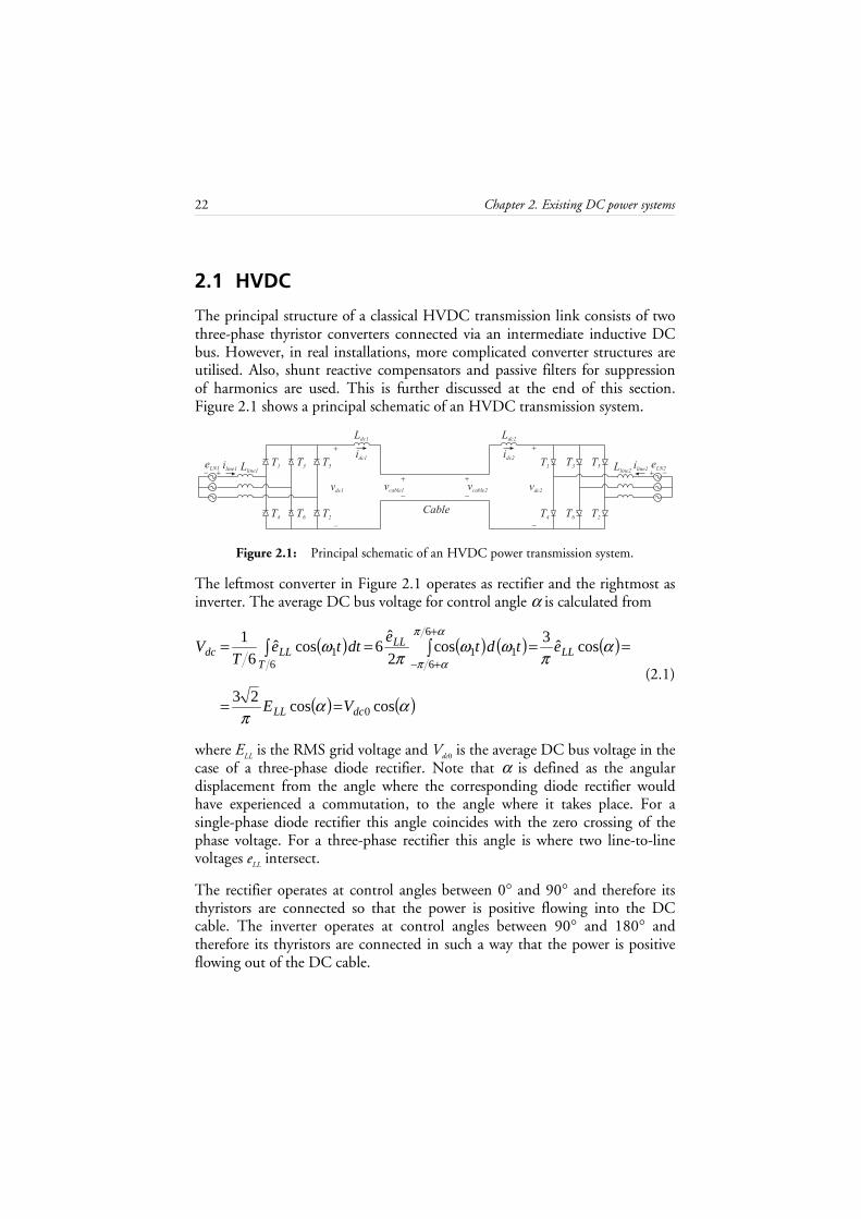
2.1 HVDC
The principal structure of a classical HVDC transmission link consists of two three-phase thyristor converters connected via an intermediate inductive DC bus. However, in real installations, more complicated converter structures are utilised. Also, shunt reactive compensators and passive filters for suppression of harmonics are used. This is further discussed at the end of this section. Figure 2.1 shows a principal schematic of an HVDC transmission system.
idc2
Ldc2
vdc2
Lline2iline2
eLN2T1
T4
T3 T5
T6 T2
Lline1iline1
eLN1
vdc1
T1
T4
T3 T5
T6 T2
idc1
Ldc1
vcable1
vcable2
Cable
Figure 2.1: Principal schematic of an HVDC power transmission system.
The leftmost converter in Figure 2.1 operates as rectifier and the rightmost as inverter. The average DC bus voltage for control angle α is calculated from
( ) ( ) ( ) ( )
( ) ( )ααπ
απ
ωωπ
ωαπ
απ
coscos23
cosˆ3
cos2
ˆ6cosˆ
6
1
0
1
6
61
61
dcLL
LLLL
TLLdc
VE
etdte
dtteT
V
==
==== ∫∫+
+− (2.1)
where ELL is the RMS grid voltage and Vdc0 is the average DC bus voltage in the case of a three-phase diode rectifier. Note that α is defined as the angular displacement from the angle where the corresponding diode rectifier would have experienced a commutation, to the angle where it takes place. For a single-phase diode rectifier this angle coincides with the zero crossing of the phase voltage. For a three-phase rectifier this angle is where two line-to-line voltages eLL intersect.
The rectifier operates at control angles between 0° and 90° and therefore its thyristors are connected so that the power is positive flowing into the DC cable. The inverter operates at control angles between 90° and 180° and therefore its thyristors are connected in such a way that the power is positive flowing out of the DC cable.

2.1 HVDC 23
Figure 2.2 shows the line-to-line voltages, DC side voltage and control angle for the rectifier and inverter, respectively.
0 5 10 15 20−600
−400
−200
0
200
400
600
t [ms]
v dc1 [
kV]
0 5 10 15 20−600
−400
−200
0
200
400
600
t [ms]v dc
2 [kV
] α eST
eRS
eTR
α
eST
eRS
eTR
Figure 2.2: Line-to-line voltages, DC side voltage and control angles for the rectifier (left)
and inverter (right) of an HVDC transmission system.
In Figure 2.3 and Figure 2.4, the R-phase line current and its spectrum are shown for the rectifier and inverter, respectively.
0 5 10 15 20−3
−2
−1
0
1
2
3
t [ms]
i line1
[kA
]
0 300 600 900 1200 1500 1800 21000
0.5
1
1.5
2
2.5
f [Hz]
i line1
,pk [
kA]
Figure 2.3: R-phase line current (left) and its spectrum (right) for the rectifier of an
HVDC transmission system.
0 5 10 15 20−3
−2
−1
0
1
2
3
t [ms]
i line2
[kA
]
0 300 600 900 1200 1500 1800 21000
0.5
1
1.5
2
2.5
f [Hz]
i line2
,pk [
kA]
Figure 2.4: R-phase line current (left) and its spectrum (right) for the inverter of an
HVDC transmission system.

24 Chapter 2. Existing DC power systems
The only major difference between the line currents in Figure 2.3 and Figure 2.4 is the phase lag of slightly less than 180° for currents flowing out from the AC grids. Consequently, the spectrums for rectifier and inverter operation are similar. The center of the line current pulse is displaced, by an angle equal to the control angle, relative to the line voltage. This means that the line current exhibits a phase lag ϕ =α. Therefore, the active P and reactive power Q are
( )( )
=
=
α
α
sin3
cos3
1,
1,
lineLL
lineLL
IEQ
IEP (2.2)
where ELL and Iline,1 are the RMS grid voltage and fundamental line current, respectively. Assuming a constant DC side current Idc, the average DC power is given by
( )απ
cos23
dcLLdcdc IEIVP == (2.3)
If the losses are neglected this implies that
( ) ( ) dclinedcLLlineLL IIIEIEPπ
απ
α 6cos
23cos3 1,1, =⇔== (2.4)
The line currents are in principle square for a high DC inductance, Ldc1+Ldc2. For a square line current (60° conduction interval), the harmonics are
=
3sin
22,
ππ
kI
kI dckline (2.5)
for k =1,5,7,11,13, etc. This is an important feature of three-phase diode and thyristor rectifiers with inductive DC links.
Classical HVDC utilises an inductive DC bus, as shown in Figure 2.1. Since the overhead lines are also inductive, the commutations take a finite time. This time is termed commutation overlap. Note that the commutation overlap affects the spectrum of a thyristor based current source converter (CSC), since the edges are slightly smoother due to the finite current derivatives. However, the reduction in harmonic content is negligible, at least for low order harmonics. Therefore, it is still a good approximation to assume that the amplitude of the harmonics fall of as 1/k where k is the harmonic order.

2.1 HVDC 25
Practical HVDC installations
Several modifications are made for practical HVDC installations, Figure 2.5, compared to the principal discussed previously.
Ldc
vcable
vdc
T1
T4
T3 T5
T6 T2
Y Y
T1
T4
T3 T5
T6 T2
Y D
Ldc
CVAr
LfAC
CfAC
LfDC
CfDC
LfDC
CfDC
Figure 2.5: Realistic schematic of an HVDC power station.
The main reasons for these modifications are related to the shape of the line currents, shown in Figure 2.3 and Figure 2.4. First, the centers of the current pulses are displaced compared to the centers of the sinusoidal pulses of the line voltages. This corresponds to a phase lag ϕ =α and yields that reactive power is consumed. To circumvent this, switched shunt capacitor banks are installed on the AC line sides of the HVDC transmission. A switched capacitor bank is formed by several capacitors connected to the line through circuit breakers in such a way that the reactive power delivered can be varied in steps. This is required since the reactive power consumed by a thyristor rectifier is
( )αsin3 1,lineLL IEQ = (2.6)
which means that the reactive power consumed is dependent both on the RMS value of the line current fundamental and the control angle. The second issue regarding the AC line currents relates to their harmonic content. Two methods are used to reduce the harmonics. First, twelve pulse thyristor converter structures are used instead of the basic six-pulse thyristor converter discussed here. A twelve-pulse converter consists of two six-pulse bridges with the DC sides connected in series. The six-pulse bridges are connected to the same AC grid via a three-winding three-phase transformer. One of the thyristor converters is connected to a delta (∆) winding and the other to a wye (Y) winding. This means that there is a 30° phase shift between the AC voltages feeding the two converters. This implies that there is a 30° phase shift between the currents fed to the converters also. Since the transformer

26 Chapter 2. Existing DC power systems
connected to the converters has a common primary side for both secondary windings, the line current on the primary side will exhibit its lowest harmonic around the 12th harmonic, i.e. the 11th and 13th order harmonics are the lowest appearing. The next pair of current harmonics appearing, are of the 23rd and 25th order. Passive shunt filters tuned to these specific harmonics are also included to further reduce the harmonic content of the AC line currents.
Traditional line-commutated, thyristor based HVDC transmission systems are difficult to build and operate cost-effectively with larger complexity than those two-terminal ones discussed above. The recently introduced VSC based HVDC transmission systems are more feasible to use as multi-terminal systems. By adopting VSCs, the problems associated with reactive power consumption and harmonics production are circumvented to a large extent.
2.2 VSC based HVDC
HVDC Light (trademark of ABB) [19] and HVDC Plus (trademark of Siemens) are basically extensions of the IGBT back-to-back converter, operating at higher power and voltage levels and with an intermediate cable between the converters. Even though this might seem as small step from a development point of view it has resulted in numerous new patents. The main reason is that the development of VSC based HVDC has forced the limits of power electronic converter technology. For example, IGBT valves withstanding more than 100 kV (through series connection) have been developed, light triggered gate or drive circuits have been developed, new cable technologies have emerged and so on. Of course, this introduction cannot provide all the details but instead focuses on the basic operation. Figure 2.6 shows a principal scheme of a VSC based HVDC transmission system.
Lline1Rline1eLN1
Cdc1 vdc1
Lline2 Rline2eLN2
Cdc2vdc2
vcable1
vcable2
Cable
Figure 2.6: Basic VSC HVDC power transmission interconnection.
From Figure 2.6 it is clear that transistor based VSCs are used for this new type of HVDC transmission system. Three-phase VSCs inherently provide the possibility of bidirectional power flow. Both the sending and receiving end converters are current controlled on the AC side, since these sides are

2.2 VSC based HVDC 27
inductive. The current controllers operate in the dq-frame as described in Appendix B. The sending end converter is responsible for controlling the DC bus voltage. To enhance the dynamic performance of DC bus voltage control, information on the output power of the receiving end converter should be fed forward to the DC bus voltage controller. The DC bus voltage controller for the converter operated as rectifier is shown in Figure 2.7.
PI+
Vdc,ref+
++
iCdc,ref+ -
vdc
iq,dc,ref
vdc
eq
iq,inv,ref
1eqpinverter
iq,ref
Figure 2.7: DC bus voltage controller for VSC based HVDC.
Figure 2.8 shows a more realistic VSC based HVDC scheme where additional AC side filters are included. This is required due to the fact that both sides of each converter are grounded and still third order injection modulation (Appendix A) is used, resulting in a zero-sequence voltage. To attenuate the current harmonics, shunt filters tuned to switching frequency are inserted between the converter AC side interface and the transformer. Figure 2.8 also shows high frequency filters (100 kHz and above) inserted at the DC side of the converter. These are required to avoid disturbances transmitted from the cable, which could interfere with broadcasting and other radio frequency equipment. Following the high frequency DC side filter, a common mode choke is inserted.
Lline
CdcvdcD Y
Cf2
Cf3vcable
Lf2
Lf3
Lf1
Cf1
Figure 2.8: Realistic VSC based HVDC converter station.
A VSC based HVDC transmission system consisting of two converters according to Figure 2.8 and a T-model of an HVDC cable (similar to the π-link shown in Figure 3.3) is investigated in simulations. The converters have a rated power of 330 MVA each and the nominal DC cable voltage is 300 kV

28 Chapter 2. Existing DC power systems
(±150 kV). The reactance of the inductive line filters equal 0.14 p.u. and the equivalent time constant of each converter including DC link capacitor is 2 ms. The rated power is the same as the one given in [19] and the other data are typical for an HVDC Light system. For the simulations, the rated line-to-line voltage is set to 150 kV. The shunt filter is tuned to switching frequency (1950 Hz) so that the fundamental current component equals 0.01 p.u., which yields appropriate values for both Lf1 and Cf1. The high frequency filter on the DC side is based on a characteristic frequency of 100 kHz and Cf2=Cf1/10. If the capacitance of Cf2 is higher, it will affect the characteristic frequency of the shunt harmonic filter. The mutual inductance of the common mode choke is set to the same value as Lf2 and the magnetic coupling factor is set to 0.99. The capacitance of Cf3 is set to Cf3=2⋅Cf2. These component values most likely defer from the ones intended for the real installation. Also the DC bus voltage controller and the converter current controllers are not equal to the ones used in the real installation. Probably the current controllers used here have higher gain than the ones in the real installation.
Figure 2.9 and Figure 2.10 show the converter power and DC bus voltage, respectively, for a time-domain simulation starting at no-load. The inverter receives an output power command equal to 165 MW (half rated power) at time t =20.0 ms. The current controller becomes aware of the increased power reference at time 20.25 ms, and calculates the desired AC side voltage reference which is applied one sample later, at time 20.5 ms. The current immediately starts to increase, but this is not noticed by the current controller before the next sample instant, at 20.75 ms. At this time, the current controller of the inverter sends a power reference to the converter acting as a rectifier, which increases its power demand. Due to the time required to establish a rectifier input power corresponding to the inverter output power, the DC bus voltage is somewhat reduced, see Figure 2.10.
20 20.5 21 21.5 22−200
−100
0
100
200
t [ms]
p i, pr [
MW
]
Figure 2.9: Inverter AC side power (black) and rectifier AC side power (grey).

2.2 VSC based HVDC 29
0 10 20 30 40 50 60260
280
300
320
340
t [ms]
v dc [
kV]
Figure 2.10: Rectifier DC side voltage.
Figure 2.11 shows the line and converter currents for both the rectifier and inverter. It is seen that the currents contain a rather high ripple, originating from switching. Especially, the converter currents exhibit a high ripple at the power increase. These ripple currents are mainly zero-sequence switching frequency components. The ripple is not so pronounced in the line currents, due to the shunt harmonic filter. The high gain of the current controllers makes this problem worse. Figure 2.12 shows the stationary line and converter currents for the inverter, together with the corresponding harmonic spectrums in the vicinity of switching frequency. The shunt filter tuned to switching frequency attenuates this component effectively.
−1500
−1000
−500
0
500
1000
1500
i line, i
conv
[A
]
0 10 20 30 40 50 60−1500
−1000
−500
0
500
1000
1500
t [ms]
i line, i
conv
[A
]
Figure 2.11: Line current (black) and converter current (grey) for the rectifier (top) and
inverter (bottom) for a load power increase. The currents are positive flowing into the AC grids.

30 Chapter 2. Existing DC power systems
0 5 10 15 20−1.5
−1
−0.5
0
0.5
1
1.5
t [ms]
i line, i
conv
[kA
]
1650 1750 1850 1950 2050 2150 22500
10
20
30
40
50
60
f [Hz]
i line,
pk, i
conv
,pk [
A]
Figure 2.12: Line current (black) and converter current (grey) for the inverter (left) and
line current spectrum (black) and converter current spectrum (grey) for the inverter at frequencies close to switching frequency (right).
In practical HVDC Light installations, resistors are connected in parallel to the inductors of the shunt filter. As a consequence, harmonics in a broader frequency spectrum are attenuated. Therefore, the harmonics around switching frequency in Figure 2.12 are attenuated more effectively in a real installation.
Feed forward of the output power of the inverter for DC bus voltage control is not used in real installations. Due to the low equivalent time constant of the converters, only low rate of change of the inverter output power is allowed.
The HVDC Light installations of comparably low rating, approximately 50 MW, are based on two-level converter technology (Figure 2.8). To achieve higher power ratings (300 MW), three-level VSCs are utilised [19].
Self-commutated two-level converters of the same type as used in the study of VSC based HVDC form, thus, a basis for the investigated multi-terminal DC distribution system. Some experience could also be found from industry and traction as mentioned in the introduction to this chapter.

31
Chapter 3
DC bus voltage control
Two different DC bus voltage control schemes are investigated. One of the methods, referred to as the communication or master/slave method, strongly relies on fast communication between the source and load converters. The output power, with sign, is calculated for each of the converters. Information on total output power is fed forward to the converters. One of the converters, the master, is responsible for controlling the DC bus voltage. Feed forward of the total output power allows for high bandwidth DC bus voltage control. The DC bus voltage controller is, however, still required during transients and to compensate for losses in the DC power system. Due to the resistive voltage drop, a proportional-integral (PI) controller is adopted in order to avoid stationary DC bus voltage error.
The other method is referred to as voltage droop control. Droop control does not require any communication at all between the converters. Instead, the DC bus voltage is measured at the source converter terminals. All the source converters contribute to balance the total power consumed by the loads and the losses of the DC power system. In common voltage droop control, the DC bus voltage decreases linearly as the output power for the converter increases, in order to give stable operation. This, of course, yields a stationary error in the DC bus voltage. Therefore, a restoration process to reduce the stationary DC bus voltage error is also discussed.
The chapter begins with an overview of the investigated system. Then the DC bus model used for the analysis is introduced. The controller structures are investigated and appropriate controller parameters are derived. The dynamic properties in the case of droop control are investigated. Last, the investigated DC bus voltage control schemes are compared in terms of load sharing.

32 Chapter 3. DC bus voltage control
3.1 Investigated system
The investigated DC distribution network model consists of five converters: three are operated as sources and two are feeding power to loads. The converters are connected to galvanically separated AC power sources or loads. The sources and loads are modeled as three-phase grids. The grids are galvanically separated, i.e. without common reference, to avoid a low-impedance path for the zero-sequence and third order harmonic currents [72].
To investigate the transient response of the DC bus voltage controllers, the power references for the power fed to the loads are changed in steps. Therefore, the dynamics of the generators, wind turbines, etc. might interfere with the dynamics of the voltage control. This is further discussed in Chapter 4, where a distributed system operated only with wind power is investigated. Figure 3.1 shows a five-converter DC power system configuration, representative for the power systems considered in the analysis.
v2
p2
v1
+
-
p1
v3
+
-
p3
v5
+
-
p5
v4
+
-
p4
+
-
Figure 3.1: The investigated DC power system configuration.
Each converter has a front interface with an inductive connection to the source. Therefore, the end interface connected to the DC bus is capacitive. Consequently, the front side of the converter is current controlled and the end side is voltage controlled. In Figure 3.2, the i th converter sub-system of the five included in the DC network is shown.
From Figure 3.2 it is clear that the considered converters are self-commutated, three-phase full-bridges. The DC bus capacitor is used to partly decouple the AC and DC systems so that a disturbance on one side is not reflected on the other side of the converter. A similar system is investigated in [66] but instead of transistor equipped VSCs, thyristor based CSCs are considered.

3.1 Investigated system 33
Lline,i Rline,ieLN,i
Cdc,ivdc,i
Figure 3.2: The converter forming the interface between the DC bus and the i th three-phase AC network, source or load.
3.2 DC bus model
There are two DC bus models discussed in this chapter. The DC bus voltage controllers are designed based on the assumption that the DC bus is purely capacitive. Therefore, a purely capacitive DC bus, with capacitance equal to the total converter DC bus capacitance, is analysed first. Then, a more accurate DC bus network with the cable segments modeled as resistive, inductive and capacitive π-links, according to Figure 3.3, is analysed.
Cs Cr
Lcable Rcable
vs
vr
is iricable
Figure 3.3: The two-converter DC bus π-link model.
In the investigation of dynamic properties, Cs and Cr in Figure 3.3 denote the total bus capacitance, i.e. cable and converter DC bus capacitance, for the sending and receiving ends, respectively. The cable capacitance is split in two equal parts, which are then added to the DC bus capacitances to give the total sending and receiving end capacitances. In the investigation on load sharing, the cable and DC bus capacitances are modeled separately.
Large-signal stability in the case of distributed converters supplying constant power loads is investigated in [2]. The result is an input LC-filter specification for the load converters, based on the maximum output power for the load converters and the total source converter output resistance. An equilibrium point criterion is used to formulate an upper limit for the source converter output resistance, which results in an intuitively understandable criterion stating that: The equivalent load resistance must be higher than the source converter output resistance. Mathematically, this is expressed as [2]

34 Chapter 3. DC bus voltage control
r
rcable P
vR
4
2
< (3.1)
with notations according to Figure 3.3. The load or receiving end power is denoted Pr. A lower bound for the source output resistance is also given in [2]. For a single output converter with a constant power load, the lower bound in the case of an ideal source is given by
r
cablecable C
LR > (3.2)
Modifications made to the latter expression to include the case with several constant power load converters are shown in [2]. However, the derived expressions are based on the assumption that the resistance Rcable is common for all the paralleled converters. In a distributed power system this is not likely. The resistance is instead distributed along the cables. Furthermore, the inductance is also a property of the cables and not inserted on purpose for filtering action. Here, only capacitors are inserted as voltage stabilisers and filters, close to both source and load converters. The stability problem therefore merely becomes a problem of selecting converter DC bus capacitors.
3.3 Controller structure
Several different DC bus voltage control schemes exist [52], of which especially two seem commonly used: master/slave and droop control. In master/slave control, active load sharing is performed and the master controller distributes power references to the other converter controllers operated as sources, e.g. the slave converters. In droop control, each source converter delivers power to the DC bus determined by the actual DC bus voltage error at the converter. Therefore, droop control does not require any communication.
Even though master/slave and droop DC bus voltage controllers operate in a different manner, the controller structures are essentially equal, which is apparent from [49]. The main difference is that in master/slave DC bus control the actual output power of the slave and load converters is also fed forward to the master, which in turn generates power references for the slave converters acting as sources. Since communication is used for the master/slave scheme, the bandwidth of the DC bus voltage control can be increased if the

3.3 Controller structure 35
communication bandwidth is sufficiently high. Thus, less energy needs to be stored in the DC bus, which implies that the DC bus capacitance can be decreased [49]. However, the system becomes more prone to interactions between the two sides of the converters when the energy storage is reduced [6]. In [73], grid interactions are handled by an active power line conditioner connected to the DC bus. This means that the DC bus capacitance can be kept low and, still, undesired interaction between the converter sides is attenuated.
DC bus voltage droop control
In common voltage droop control, the bus voltage decreases linearly as the output current, or in some cases power, for the converter increases, in order to give stable operation (Figure 3.4). This, of course, results in a stationary error in the voltage level.
Vdc
Vdc,ref0
Idc
Figure 3.4: Steady state droop characteristic.
The controller structure for DC bus voltage control is shown in Figure 3.5. A proportional (P) controller is used for the droop scheme, similar to the PI-controller derived in [6] for back-to-back converter DC link voltage control. This controller structure is implemented in all converters, intended for power flow into the DC bus. The reason for this is to be able to distribute the total load between the sources when droop control is used. Note that several converters are used to support the power flow, which is not evident from Figure 3.5.
To simplify the investigation, a simple system with only one source and one load converter is considered. This is extended to cover the case with several source and load converters. The measured DC bus voltage is low-pass filtered (Figure 3.5) to attenuate interactions between the negative-sequence current of the AC side and the DC bus voltage control discussed in [67], and to facilitate controller pole-placement design [6].

36 Chapter 3. DC bus voltage control
G (s)P
KV (s)sV (s)dc,ref
G (s)conv
I (s)s,ref
P (s)ref,ext
I (s)ref,ext
I (s)s
1/sCs
1/ +1/Z Zcable r
G (s)lp
I (s)cable
V (s)s,lp
&&lp
lps+
1V (s)s
Figure 3.5: Structure of the DC bus voltage droop controller. The source converter current is denoted Is and the cable current Icable.
The DC bus voltage controller for the droop scheme is written
( )lpsrefdcrefs vVKi ,,, −= (3.3)
In the case of a purely capacitive DC distribution system, i.e. when Lcable=0 H, Rcable=0 Ω and Cdc=Cr+Cs (Figure 3.3), the closed loop transfer function from DC bus voltage reference to actual voltage is written
( )( )
( )dclplp
lpdccl
CKss
sCKsG
ωωω
++
+=
2)( (3.4)
The effects of non-zero cable impedance are shown in the next section, where dynamic properties are examined. In the case of a purely capacitive DC distribution system, the current at the receiving end is expressed as
Cdcsr iii −= (3.5)
which in the case of a single source gives a droop function according to
( ) ( )( )( )
( ) ( )( )( )
( )sICKss
sCsV
CKss
sCKsV r
dclplp
lpdcrefdc
dclplp
lpdcs ωω
ωωω
ω++
+−
++
+=
2,2
1 (3.6)
The steady state droop impedance or resistance is, thus, written
K
Rdroop1= (3.7)

3.3 Controller structure 37
The characteristic polynomial of the closed loop transfer function is given by
( ) ( )dclplp CKsssp ωω ++= 2 (3.8)
The desired characteristic polynomial can be expressed as
( ) 22 2 nnn sssp ωωζ ++= (3.9)
and is fulfilled for
( ) dclp
n
CK ωζ 22
1= (3.10)
The closed loop bandwidth is given by
lpn
n ωζ
ω2
1= (3.11)
It is apparent that a high damping of the poles of the closed loop transfer function requires a high DC distribution bus capacitance. Here, the poles are chosen to obtain a performance corresponding to the one of a Butterworth filter, which means that the damping is selected as
2
1=nζ (3.12)
This choice of damping requires a rather moderate DC distribution bus capacitance without making the system oscillatory. The last point is important since the DC distribution bus is not purely capacitive. This implies that it is not advisory to make the simplified system oscillatory and then introduce non-idealities into the system.
From the equations above, the gain is expressed as
dclpCK ω2
1= (3.13)
Assume that each converter corresponds to a virtual resistance, with a base value equal to

38 Chapter 3. DC bus voltage control
n
refdcn P
VR
2,= (3.14)
In the case of droop control, the DC current at rated load for rectifier operation increases due to the decreased DC bus voltage caused by the droop characteristic
( ) ( )n
ndc
nrefdc
nndc
I
V
PI
δδ −=
−=′
11,
,, (3.15)
where δn is the relative converter output voltage droop at rated power. Since the voltage droop corresponds to the gain, it is found that
( )
( )
( ) nnn
n
ndc
nrefdc
dclp
ndroop R
I
V
CKR δδ
δ
δω
ζ −=
−
=== 1
1
21
,
,2
(3.16)
This is rewritten to
( ) ( ) ( )systemnlp
n
dcnlp
nnn CR ,
22 12121
τωζ
ωζδδ ⋅=⋅=− (3.17)
where τn,system is the time constant of the system. Now, it is assumed that only half the DC bus capacitance required is located at the source converter. The other half is located at the receiver or load converter. This means that
2,dc
converterdcrsC
CCC === (3.18)
and the converter time constant is
22
,,,
systemndcnconverterdcnconvertern
CRCR
ττ === (3.19)
This gives the following specification for each converter, both source and load
( ) nnlp
nconvertern δδω
ζτ−
⋅=1
12 2
, (3.20)

3.3 Controller structure 39
This implies that all converters connected to the DC distribution system should be equipped with DC bus capacitors selected according to
( ) nnlp
n
refdc
nconverterdc
V
PC
δδωζ
−⋅⋅=
1
12 2
2,
, (3.21)
Note that for a multi-converter system all the source converters should have the same stationary characteristic to obtain proper, i.e. democratic, load sharing. If the DC side capacitor of each converter is selected according to the expression above, this is fulfilled. Furthermore, for an ideal cable, i.e. without any impedance other than the DC side capacitors, the system transfer function is the same as for the two-converter system when the total rated power of the sources equal the one of the loads. For converters with the following data
==
≈==
05.0
21
rad/s 188rad/s 302
V 750,
n
n
lp
refdcV
δζω
(3.22)
it is found that each converter, source and load, should have a DC side capacitance to rated power ratio given by
F/kW 199,
, =convertern
converterdc
P
C (3.23)
Note that the rated power is given for inverter operation at a DC link voltage equal to Vdc,ref . According to [4], the converter losses decrease for rectifier operation compared to inverter operation (Appendix C). This implies that the maximum allowable rectifier power is higher than the maximum inverter power based on the assumption that the converter losses are equal in the two cases. It is shown in a later section that for the IGBT module Semikron SKM300GB123D, the rectifier power resulting in the same amount of converter losses as inverter operation at rated load, is around 17% higher for droop control than the rated power for inverter operation. The higher rated power at rectifier operation is used to compensate for DC bus losses.
The DC bus capacitance required for each converter by applying this method is higher compared to what has been reported in other work on the same topic [67]. Therefore, the converter proposed here is more bulky. However, the DC

40 Chapter 3. DC bus voltage control
link capacitance for each converter is lower than twice the one of a regular three-phase converter, e.g. for motor drive applications. Furthermore, the magnitude of the DC bus voltage oscillations observed for an unbalanced AC load [67] is inversely proportional to the DC bus capacitance [6]. The oscillation appears at twice the fundamental frequency of the unbalanced AC network [6][67], which means that introducing a low-pass filter with break-over frequency lower than the oscillation frequency effectively attenuates the problem. For the 75 kW DUAL battery charger [5], a DC bus variation of 5% of the rated DC link voltage of 750 V is allowed in the specification. This requires a DC link capacitance of 2.45 mF, according to Appendix D. The sinusoidal 100 Hz component has an amplitude of 58 A (41 A RMS). Furthermore, two 450 V capacitors has to be connected in series, which implies that DC link capacitors of 4.7 mF should be sufficient. However, the RIFA PEH 4.7 mF capacitors only sustain between 13.5 and 15.9 A RMS at 100 Hz. Therefore, at least three such branches are required to avoid thermal overloading of the capacitors, which corresponds to 7.05 mF. In the implemented DUAL battery chargers, five such branches are used to provide margin to the absolute maximum temperature, which yields a total DC link capacitance of 11.75 mF. This should be compared to the 15 mF required for a 75 kW DC distribution converter according to the selection method proposed here.
DC bus voltage control with droop error restoration
There have been attempts to include error restoration in droop control [7]. This could be done by, for example, using DC bus voltage PI-control instead of the P-controller shown in Figure 3.5. If a PI-controller is adopted in the scheme in Figure 3.5, the closed loop transfer function from DC bus voltage reference to actual voltage for each converter operated as a source, i.e. supporting the DC bus voltage, is written
( )( )( )
dci
lp
dc
lplp
lpidci
cl
CT
Ks
C
Kss
ssTCT
K
sG ωωω
ω
+++
++=
23
1
(3.24)
where Ti is the time constant of the integral part. The controller parameters are selected in a similar way as for the regular droop scheme to compare the controller action. Therefore, the closed loop transfer function should have a characteristic polynomial given by

3.3 Controller structure 41
( ) ( )( )nnnndci
lp
dc
lplp sss
CT
Ks
C
Ksssp ωωωζ
ωωω +++=+++= 2223 2 (3.25)
This gives the following controller parameters
( )
+=
+=
+=
lp
ni
lpdcn
lpn
n
T
CK
ωζ
ωζ
ωζ
ω
221
21
1
211
(3.26)
For poles located according to a corresponding third order Butterworth filter, a relative damping
21=nζ (3.27)
is required. This gives the following controller parameters
=
=
=
lpi
lpdc
lpn
T
CK
ω
ω
ωω
42
12
1
(3.28)
Note that the gain is the same as for the P-controller used for regular droop control. Thus, the same controller can be used in both cases and the only difference is whether the integral part should be added or not. For PI-control, the source converter output voltage is written
( ) ( )( ) ( )( )( ) ( ) ( )
( ) ( )( ) ( ) ( )sI
TCKsCKss
ssC
sVTCKsCKss
TssCKsV
r
idclplpdclp
lpdc
refdc
idclplpdclp
ilpdcs
⋅+++
+−
−⋅+++
++=
ωωω
ω
ωωω
ω
23
,23
1
1
(3.29)

42 Chapter 3. DC bus voltage control
Note that the steady state source impedance is equal to zero, which is the main advantage gained by the use of PI-control. One major drawback exists with decentralised PI DC bus voltage control, resulting from the fact that several sources equipped with integral parts control the same quantity, the DC bus voltage. In automatic control terms this results in that both observability and controllability are lost [80]. This implies that any non-ideal feature of the DC distribution network, for example the bus resistance, will force the sources to exhibit poor load sharing.
One way of partly circumvent this problem is to inhibit updating of the controller integral part when the DC bus voltage at the particular source is inside a specified dead-band [7]. The dead-band ought to be proportional to the voltage drop along the DC bus between the source converter in question and a predetermined point in the DC network common to all source converters. Also the transient behaviour is affected by the DC bus impedance and since an integrator corresponds to a dynamical state, the imbalance during the transients remains in stationary conditions. This is partly solved by applying a load dependent integral time constant, so that a converter connected to a source with high relative loading will have a weak integral part. Consequently, it is only updated to a limited extent for a new load situation. This has been successfully utilised for wind power farms operating directly on the three-phase AC grid [7]. Simulations of a DC distributed power system with source converters with integral parts given by
−=
nlpi P
PT
21
4
ω (3.30)
are shown in the section on load sharing. Note that the power is considered as positive flowing out of the converter AC side. Therefore, the time constant above increases the more power the source delivers to the DC system.
Master/slave DC bus voltage control
In the master/slave DC bus voltage control scheme investigated here, only the master is responsible for voltage control. The voltage controller for the master converter is shown in Figure 3.6. Information on actual power for all the other converters is fed forward to the master, where appropriate power references for the slaves, i.e. the other converters operated as sources, are calculated. Even if not used here, the voltage controller output could be included in the slave power references.

3.3 Controller structure 43
G (s)PI
K, Ti
V (s)dcV (s)dc,ref
G (s)conv
P (s)load
I (s)dc
1/sCdc
G (s)lp
V (s)dc,lp
&&lp
lps+
1V (s)dc
I (s)Cdc,ref
Figure 3.6: Structure of the master/slave DC bus voltage controller. The source converter current is denoted Idc.
In Figure 3.6, a PI-controller is adopted for master/slave DC bus voltage control. The closed loop transfer function from DC bus voltage reference to actual voltage is equal to the one for droop control with voltage error restoration, i.e.
( )( )( )
dci
lp
dc
lplp
lpidci
cl
CT
Ks
C
Kss
ssTCT
K
sG ωωω
ω
+++
++=
23
1
(3.31)
Note that for this master/slave scheme, only one converter serves to control the DC bus voltage. Still, several converters are used to support the power flow but their power reference is provided by the over-lying controller structure. The load power fed forward in Figure 3.6 is, thus, the sum of the output power of all the other converters in the DC system.
Also for master/slave DC bus voltage control, the closed loop transfer function has poles located as a corresponding third order Butterworth filter, to obtain similar dynamic properties. Consequently, the controller parameters are given by (3.28) for the master/slave scheme. However, note that the gain is based on the total DC bus capacitance in the case of master/slave control. For droop control, the gain is calculated based on Cdc=2⋅Cdc,converter for each source converter. For master/slave control, the source converter output voltage is written

44 Chapter 3. DC bus voltage control
( ) ( )( ) ( )( )( ) ( )( ) ( )( )
( )sVsss
sssV refdc
lplplp
lplplpdc ,
22 222
42⋅
+++
++=
ωωω
ωωω (3.32)
if the power fed forward is accurate and the DC bus is purely capacitive.
3.4 Cable impedance
In this section the effect of cable impedance on voltage droop control is studied. The investigation focuses on regular droop control, i.e. without voltage error restoration.
Steady state characteristics
For simplicity, assume a network consisting of only one source and one load, operating in steady state. The latter assumption implies that the network can be regarded as purely resistive and that only the steady state droop characteristic has to be considered, see Figure 3.7.
Rr
Rdroop Rcable
Vdc,ref
Vr
Ir
Figure 3.7: The simplified Thevenin equivalent for steady state analysis.
The current supplied to the load, with reference to Figure 3.7, is written
r
r
cabledroop
rrefdcr V
P
RR
VVI =
+−
= , (3.33)
This is rewritten to form a second order algebraic equation
( ) 0,2 =++− rcabledrooprrefdcr PRRVVV (3.34)
If this is expressed in one common p.u. system, e.g. the one of the source, it is found that
( ) ( ) ( )( ) 0111 2 =+−+−−− rcablennrr prδδδδ (3.35)

3.4 Cable impedance 45
where (1-δr) and pr are the p.u. receiving end voltage and power, respectively. The p.u. cable resistance is denoted rcable. The p.u. base is given in Appendix D. The stable solution to this equation is written
( )( ) rcablennr pr+−−−= δδδ 14
1
2
1 (3.36)
Since the resistors form a voltage-dividing network, the source voltage is
( )rrefdccabledroop
drooprefdcs VV
RR
RVV −⋅
+−= ,, (3.37)
The relative voltage reduction at the sending end is thus
( )( )
( )( ) ( )( )
+−−−⋅
+−−=
=+−
−=
rcablenncablenn
nn
rcablenn
nns
prr
r
δδδδ
δδ
δδδ
δδδ
141
21
1
1
1
1
(3.38)
The risk of encountering converter over-modulation due to a too low DC bus voltage is the main reason for investigating the DC bus voltages at different points in the network. The minimum DC link voltage is determined from the required load voltage at the converter output terminals, including the voltage drop across the output filter. For a three-phase AC load expressed in rotating reference dq-coordinates (Appendix A, Appendix B), the stationary converter output voltage is written
++=++=
−=+−=
lineq
lineqdlineqlineq
qline
qlinedqlinedlined
ee
QL
e
PReiLiRu
e
PL
e
QReiLiRu
11
11
ωω
ωω (3.39)
In the expression above, P and Q denote active and reactive power, positive flowing from the converter into the AC system. The AC grid angular frequency is denoted ω1=2πf1 and the voltage vector qd
dq jeee +=. According
to Appendix A, 0=de . The AC line filter inductance and resistance are denoted Lline and Rline (Figure 3.2). The output voltage and current of the

46 Chapter 3. DC bus voltage control
converter are denoted, qddq juuu +=
and qddq jiii +=
, respectively. Neglecting the resistive voltage drop gives
+=+≈
−=−≈
lineqdlineq
qlineqlined
ee
QLeiLu
e
PLiLu
11
11
ωω
ωω (3.40)
The converter output voltage magnitude is given by
2
1
2
122
++
≈+= q
qline
qlineqd e
e
QL
e
PLjuuu ωω
(3.41)
If this is expressed in line-to-neutral RMS voltages, it is found that
2
1
2
12 33
++
≈ LN
LNline
LNline E
E
QL
E
PLU ωω (3.42)
The maximum allowable RMS line-to-neutral voltage to avoid over-modulation in stationary operation is given by
6
dcmax
VU = (3.43)
for symmetrical voltage references, i.e. when space vector pulse width modulation (SVPWM) [35] is used, see Appendix A. If it is assumed that the reactive power Q equals zero, the limiting case is written
22
1
2 3
6 LNLN
linedc E
E
PL
V +
= ω (3.44)
which is valid when the converter is operating as inverter as well as for rectifier operation. Thus, for the receiving end converter (index r) of the DC network the limiting case is
2,
2
,,,1
2 3
6 rLNrLN
rrliner
r EE
PL
V +
= ω (3.45)

3.4 Cable impedance 47
Consequently, the receiving end DC bus voltage in p.u. is given by
( ) 2,
2
,
,21 rLLrrLL
rliner ep
e
x+
⋅≥−δ (3.46)
where eLL,r and xline,r are p.u. values of the line-to-line voltage and line reactance of the receiving end, respectively. The p.u. base is given in Appendix D. Rearranging the terms yields
2,
2
,
,21 rLLrrLL
rliner ep
e
x+
⋅−≤δ (3.47)
Rearranging (3.36) gives the cable resistance
( ) nnrr
cable pr δδδ −−
−−= 1
2
1
4
112
(3.48)
The maximum cable resistance allowed, is found from combining the last two expressions
( ) nnrLLrrLL
rline
rcable ep
e
x
pr δδ−−
−+
⋅−≤ 1
2
12
4
112
2,
2
,
, (3.49)
The p.u. line reactance used in [6] is approximately equal to
0838.0=linex (3.50)
which is required to fulfil the standard IEC 1000-3-2, if ELN =230 V and Vdc,ref =750 V at a switching frequency of 4.95 kHz. Assuming operation at rated power, i.e. pr=1, gives
214.0≤rδ (3.51)
and the maximum allowable cable resistance in p.u.
120.0≤cabler (3.52)

48 Chapter 3. DC bus voltage control
Furthermore, this corresponds to a source voltage given by the droop
( )
( ) 06.01
1 =+−
−= rcablenn
nns r
δδδ
δδδ (3.53)
This means that the p.u. power supplied from the source equals
( )( ) 196.11
1 =−−=
nn
sssp
δδδδ
(3.54)
which implies that the 17% higher rated power possible at rectifier operation for the same amount of losses as for rated inverter operation is not sufficient. On the other hand, a DC network design without margins to avoid over-modulation, is not likely. Also, cable losses approximately equal to 0.2 p.u. seems high. The p.u. droop characteristic for a three-phase converter based on Semikron SKM300GB123D modules, including over-modulation and loss limits, is shown as a function of current in Figure 3.8 and of power in Figure 3.9.
−2 −1.5 −1 −0.5 0 0.5 1 1.5 20.7
0.750.8
0.850.9
0.951
1.051.1
idc
v dc
Figure 3.8: Per unit iv droop characteristic, including over-modulation and loss limits.
−1.5 −1 −0.5 0 0.5 1 1.50.7
0.750.8
0.850.9
0.951
1.051.1
pdc
v dc
Figure 3.9: Per unit pv droop characteristic, including over-modulation and loss limits.

3.4 Cable impedance 49
Figure 3.8 and Figure 3.9 are based on the following converter data: Sn=75 kW, Vdc,ref =750 V, ELN =230 V, 50 Hz and Lline=2 mH, according to (3.50). Furthermore, the converter operates in such a way that unity power factor is obtained for the AC network. The loss limits are calculated from the method given in Appendix C and the over-modulation limit is calculated from (3.44).
From Figure 3.9, the increased power handling capability for rectifier operation at a semiconductor loss level equal to the rated appears to be close to 17%, as previously mentioned.
Dynamic properties
An impedance specification for individual loads of DC distribution systems, based on the small-signal stability criterion, is presented in [21]. Here, stability is studied in terms of location of the closed loop poles and the root-locus [51] as a function of the cable parameters. Therefore, the cables are from now on modeled as resistive and inductive, with the cable capacitance neglected or lumped with the converter DC side capacitance, i.e. with
( )1+⋅=+= cablecablecablecablecable sRRsLZ τ (3.55)
The equivalent impedance of the receiving end is expressed as
11 +
=+
=r
r
rr
rr s
R
CsR
RZ
τ (3.56)
The impedance seen from the source converter (including its DC side capacitor) is written
( )1
1+
++⋅=+=r
rcablecablercable s
RsRZZZ
ττ (3.57)
Here, the cable and the equivalent receiving end resistances are expressed as
( )
=⋅−==
=
nrn
refdc
r
r
r
rr
ncablecable
RrP
V
pP
VR
RrR
2,
22 1 δ (3.58)
This means that the corresponding time constants are

50 Chapter 3. DC bus voltage control
( )
⋅=⋅−==
⋅=
converternpurconverternr
rrrr
converternpucablecable
pCR ,)(,
2
,)(
1 τττδτ
τττ
(3.59)
where τ(pu) denotes p.u. time constant. The impedance is thus written
( )( )( )( )111/1
+++⋅+
=+ rcablercabler
rrcable ssrr
s
RZZ ττ
τ (3.60)
The source converter output voltage is divided between the cable impedance and the equivalent impedance of the receiving end converter, which gives
( )( )( )
++
++
⋅=
+++=
+=
cable
r
rcablercablercable
r
cable
rcablercablercable
r
S
R
r
rss
r
r
ssrrZZ
Z
V
V
1111
11
111/
1
2
ττττττ
ττ
(3.61)
Assuming complex poles, the characteristic polynomial is written
22 2)( ooo sssp ωωζ ++= (3.62)
which results in
+⋅
+⋅=
+⋅=
rcable
cable
purpucable
purpucableo
cable
r
purpucableconverterno
rr
r
r
r
)()(
)()(
)()(,
2
1
11
ττ
ττζ
τττω
(3.63)
Assuming
( )
basepuon
nnlppuoo ωω
ζδδωωω ⋅=
−⋅= )(2)(2
1 (3.64)
gives a cable constant of

3.4 Cable impedance 51
+⋅=
cable
r
purpuopucable r
r1
1
)(2
)()( τω
τ (3.65)
Since the measured DC bus voltage is low-pass filtered with break-over frequency ωlp at the sending converter terminals, it is desirable that
( ) nn
npuo δδ
ζω−
≥1
2 2
)( (3.66)
The main purpose of (3.61)-(3.66) is to provide a numerical base for the further investigation where the limiting case with cable resistance equal to
06.0=cabler (3.67)
is assumed. This gives the receiving end voltage
( ) ( )( ) V 658877.014
1
2
11 ==+−−+=− rcablennr prδδδ (3.68)
at rated output power. Therefore, the receiving end p.u. resistance is given by
( )
770.01 2
=−=r
rr p
rδ
(3.69)
Note that the p.u. resistance and time constant of the receiving end are equal if the cable capacitance is neglected, i.e.
( )
r
rpurr p
r2
)(1 δτ −=≡ (3.70)
Therefore, the maximum allowable time constant, according to (3.66), is given by
( )
( )0405.0
1
12
1
1
2
2
2
2)(
)(
=
+
−⋅
−=
=+⋅=
cabler
r
n
nn
rcable
rcable
puopucable
r
p
rr
rr
δζδδ
ωτ
(3.71)

52 Chapter 3. DC bus voltage control
This means that the cable resistance and inductance are
⋅⋅⋅=⋅=
=⋅=−
nconverterncablecablecable
nncablecable
RRL
RRrR
,310432.2
06.0
ττ (3.72)
For a 750 V, 100 kW system, this is equivalent to cable parameters
=
Ω=
mH528.1
3375.0
cable
cable
L
R (3.73)
The simulation result for this case is shown in Figure 3.10. Note that the cable data investigated here correspond to rcable=0.06 p.u. and lcable=0.0024 p.u., i.e. τcable=0.04 p.u. All time-domain simulations in this section are carried out using DYMOLATM with switch-mode converter models utilising vector current controllers according to Appendix B and voltage droop controllers according to (3.3). The voltage droop controller gain (3.10) for each source converter is calculated based on Cdc=2Cs since a load converter of the same rated power has Cr=Cs (3.18). The AC side current reference for the source converter is calculated from the droop current reference based on the assumption that the converter is loss-less.
625
650
675
700
725
750
775
v s, vr [
V]
0 100 200 300 400 500−150
−100
−50
0
50
100
150
t [ms]
p s, pr [
kW]
Figure 3.10: DC bus voltage (top) and power (bottom) of the sending (black) and receiving
(grey) end converters at an output power step from zero to rated power.

3.4 Cable impedance 53
In Figure 3.10 it is shown that the stationary voltage is lower than expected (a few Volts). This is due to the fact that rated power is transmitted to the three-phase grid, i.e. the losses in the line side filter have to be added to the power supplied to the DC side of the converter. This also implies that the equivalent load resistance, Rr, is lower than expected from previous calculations.
Now, the system is examined by means of pole-zero plots. The transfer function Vs/Vdc,ref , according to Figure 3.5, is investigated in MATLABTM for different cable parameters and receiving end loading. MATLABTM is used since the transfer function is significantly more complicated than (3.4) when cable parameters are included. The characteristic polynomial for this two-converter system is of the fourth order and analytical expressions for the poles are not possible to derive. Note that (3.61) cannot be used in the stability analysis since the source converter output impedance, including Cs, is not taken into account. Instead, (3.36) is used to calculate the receiving end voltage for the actual loading. An equivalent load resistance is calculated from δr and pr. The transfer function Zcable+Zr, appearing in Figure 3.5, is calculated according to (3.57). The total impedance seen from the converter is calculated as the source converter DC side capacitance Cs in parallel with Zcable+Zr, which also forms the transfer function from Is to Vs (Figure 3.5). The converter in Figure 3.5 is considered having a transfer function Gconv(s)=1 for the frequencies of interest and the external power reference Pref,ext is set to zero.
Figure 3.11 shows the pole-zero plot for the system with the same parameters as for Figure 3.10, at no-load (small markings) and at rated load (large markings). It is obvious from Figure 3.11 that the actual loading of the system is of minor importance for stability, which is due to the fact that the equivalent load resistance is considerably higher than the cable impedance.
−250 −200 −150 −100 −50 0−500
−250
0
250
500
Real Axis
Imag
Axi
s
ρ1
ρ3
ρ4
ρ2
Figure 3.11: Pole-zero map for cable data rcable=0.06 p.u. and lcable=0.0024 p.u., which give τcable=0.04 p.u. Small markings are used for no-load (pr=0) and large markings for receiver output power equal to rated sender power (pr=1.0).

54 Chapter 3. DC bus voltage control
To investigate the robustness against parameter uncertainty, rcable is varied from 0.01 to 0.12 p.u. and the cable time constant is varied from 0.02 to 0.4 p.u. The root-locus is investigated for a case where the receiving end power is approximately equal to rated power of the sending end converter, i.e. pr is equal to one. This is not a strong limitation since it has been found that the load level affects the pole-zero map to a barely noticeable extent. Figure 3.12 and Figure 3.13 show the resulting root-locus for the poles ρ1 and ρ3, respectively (Figure 3.11). The two other poles, ρ2 and ρ4, are complex conjugate pairs of the ones in Figure 3.12 and Figure 3.13, and therefore not included.
−250 −200 −150 −100 −50 00
250
500
750
1000
Real Axis
Imag
Axi
s
lcable
rcable
= 0.12
τcable
= 0.02
τcable
= 0.4
rcable
= 0.06
rcable
= 0.01
Figure 3.12: Root-locus for pole ρ1 at pr=1.0 p.u. The traces are from top to bottom: rcable=0.01, 0.06 and 0.12 p.u. The dotted lines show constant τcable=0.02, 0.04, 0.05, 0.1, 0.2 and 0.4 p.u. from left to right.
−150 −125 −100 −75 −50 −25 00
25
50
75
100
Real Axis
Imag
Axi
s
lcable
τcable
= 0.02 τcable
= 0.4
rcable
= 0.06
rcable
= 0.12
rcable
= 0.01
Figure 3.13: Root-locus for pole ρ3 at pr=1.0 p.u. The traces are from top to bottom: rcable=0.01, 0.06 and 0.12 p.u. The dotted lines show constant τcable=0.02, 0.04, 0.05, 0.1, 0.2 and 0.4 p.u. from left to right. Note that the pole is real valued for low lcable when rcable=0.12 p.u.

3.4 Cable impedance 55
From Figure 3.12 and Figure 3.13, it is concluded that a low cable resistance results in a moderately damped system, which is also expected. This is further seen from the overshoot appearing in the DC bus voltage response resulting from a load power step at low cable resistance and time constant, see Figure 3.14. The overshoot is due to the ρ3-ρ4 pole pair, resulting from the selected damping (3.12).
625
650
675
700
725
750
775
v s, vr [
V]
0 100 200 300 400 500−150
−100
−50
0
50
100
150
t [ms]
p s, pr [
kW]
Figure 3.14: DC bus voltage (top) and power (bottom) of the sending (black) and receiving (grey) end converters at an output power step from zero to rated power when rcable=0.01 p.u., lcable=0.0002 p.u. and, thus, τcable=0.02 p.u.
For a long time constant of the cable, the situation is worse with a superimposed oscillation on the overshoot (Figure 3.15). The oscillation frequency is close to 40 Hz, corresponding to the location of ρ1 (and ρ2) in Figure 3.12. On the other hand, when rcable=0.12 p.u., the system is well damped but the receiving end converter operates at the limit of over-modulation for rated output power. Furthermore, the cable losses are high, around 20%, as discussed earlier. Therefore, such a high cable resistance is not recommended.
From this investigation it is concluded that the DC bus voltage droop controller operates as intended for practical cable parameters. The cable resistance is limited by the risk of converter over-modulation. The investigated cable inductance most likely covers practical situations.

56 Chapter 3. DC bus voltage control
625
650
675
700
725
750
775
v s, vr [
V]
0 100 200 300 400 500−150
−100
−50
0
50
100
150
t [ms]
p s, pr [
kW]
Figure 3.15: DC bus voltage (top) and power (bottom) of the sending (black) and receiving (grey) end converters at an output power step from zero to rated power for the case with rcable=0.01 p.u., lcable=0.004 p.u. and, thus, τcable=0.4 p.u.
3.5 Load sharing
Load sharing for a five-converter DC ring bus (Figure 3.1) is investigated in simulations. The network and converter parameters are given in Table 3.1. Cable segment 1 (Figure 3.3) is connected between converter 1 and 2, segment 2 between converter 2 and 3, etc. Since this is a ring bus, segment 5 is connected between converters 5 and 1. To determine an appropriate cable resistance (Rcable, Table 3.1), it is assumed that the cable length of each segment is 100 m and that the maximum current density is 4 A/mm2 even if the ring bus is broken. The cable inductance (Lcable) is calculated assuming a distance between the centers of the conductors equal to twice the conductor diameter. This assumption is also used in the calculation of the cable capacitance (Ccable).
Both stationary and transient load sharing are investigated for master/slave and droop DC bus voltage control. Load sharing in the case of droop control with voltage error restoration is also investigated. Three converters, 1, 3 and 5 in Table 3.1, are operated as sources. Converters 2 and 4 are operated as loads. The sources and loads are modeled as three-phase AC grids, which are galvanically separated. Consequently, the dynamics of sources and loads are not taken into account in this investigation.

3.5 Load sharing 57
Table 3.1: Simulation model data.
Converter no. i 1 2 3 4 5 Rated power Sn [kVA] 25.0 100.0 50.0 50.0 75.0 Line-to-neutral voltage ELN [V] 230 230 230 230 230 Line frequency fn [Hz] 50 50 50 50 50 Switching frequency fsw [kHz] 7.5 7.5 4.95 5.0 4.95 Line inductance Lline [mH] 6.0 1.7 3.0 3.40 2.0 Line resistance Rline [Ω] 0.5 0.25 0.5 0.25 0.5 DC bus capacitance Cdc [mF] 5.0 20.0 10.0 10.0 15.0 Cable capacitance Ccable [nF] 5.27 5.27 5.27 5.27 5.27 Cable inductance Lcable [µH] 52.7 52.7 52.7 52.7 52.7 Cable resistance Rcable [mΩ] 64.7 64.7 64.7 64.7 64.7 DC bus voltage reference Vdc,ref [V] 750 750 750 750 750
The investigation starts at a condition where the load converters, 2 and 4 (Table 3.1), operate at no-load. From the initial no-load operating point, the output power of converter 2 increases by 50% of rated power at t =100 ms and the output power of converter 4 increases by 50% of rated power at t =200 ms. This means that for an ideal system, i.e. with zero cable impedance, the source converters should also be loaded to half their rated power at the end of the simulation.
In all the figures shown in this section, black curves denote source converter quantities and grey denote load converter quantities. Therefore, quantities belonging to converter sub-system 1 are solid black, 2 are solid grey, 3 are dashed black, 4 are dashed grey, and 5 are dash-dotted black.
DC bus voltage droop control
Figure 3.16 shows the simulation result for load sharing in the case of DC bus voltage droop control with a P-type controller, i.e. without voltage error restoration. It is seen in Figure 3.16 that load sharing works properly both in stationary and transient conditions. The source converters are loaded to approximately 0.6 p.u. each, on the unit base. The barely noticeable, but present, difference in relative loading is a result of the resistance of the cable segments. As expected, voltage regulation is poor. However, as long as the converters do not operate in over-modulation this is not a problem. As discussed earlier in this chapter, over-modulation is avoided by selecting a distribution bus with a moderate resistance.

58 Chapter 3. DC bus voltage control
720
730
740
750
760
v 1, v2, v
3, v4, v
5 [V
]
0 50 100 150 200 250 300−100
−50
0
50
100
t [ms]
p 1, p2, p
3, p4, p
5 [kW
]
Figure 3.16: DC bus voltage (top) and power (bottom) for DC bus voltage droop control in the case of an output power increase of 0.5 p.u. of rated load converter power at t=100 ms for converter 2 and t=200 ms for converter 4 starting from 0 p.u. in both cases.
DC bus voltage droop control with error restoration
Figure 3.17 and Figure 3.18 show the simulation results for load sharing in the case of DC bus voltage droop control with a PI-controller, i.e. including voltage error restoration. The simulation result of Figure 3.17 is for a controller equipped with a constant integration time constant and the one of Figure 3.18 with a load dependent integration time constant. The integration is inhibited when the DC bus voltage at each source is inside a dead-band of 5 V located on both sides of the DC bus voltage reference, 750 V.
From Figure 3.17 and Figure 3.18 it is seen that load sharing is poor in both cases. The loading of the source converters in the case of DC bus voltage droop control with error restoration is roughly between 0.5 and 0.7 p.u., on the unit base, according to Figure 3.17 and Figure 3.18. Load sharing might be enhanced if different voltage error dead-bands are specified for each source converter. However, in a mesh network, like the ring bus investigated here, this is a complicated task. On the other hand, voltage regulation is enhanced compared to regular droop control, due to the integral part. Still, appropriate load sharing is considered as being of more concern.

3.5 Load sharing 59
720
730
740
750
760
v 1, v2, v
3, v4, v
5 [V
]
0 50 100 150 200 250 300−100
−50
0
50
100
t [ms]
p 1, p2, p
3, p4, p
5 [kW
]
Figure 3.17: DC bus voltage (top) and power (bottom) for DC bus voltage droop control with error restoration in the case of an output power increase of 0.5 p.u. of rated load converter power at t=100 ms for converter 2 and t=200 ms for converter 4 starting from 0 p.u. in both cases.
720
730
740
750
760
v 1, v2, v
3, v4, v
5 [V
]
0 50 100 150 200 250 300−100
−50
0
50
100
t [ms]
p 1, p2, p
3, p4, p
5 [kW
]
Figure 3.18: DC bus voltage (top) and power (bottom) for DC bus voltage droop control with error restoration in the case of an output power increase of 0.5 p.u. of rated load converter power at t=100 ms for converter 2 and t=200 ms for converter 4 starting from 0 p.u. in both cases.

60 Chapter 3. DC bus voltage control
Master/slave DC bus voltage control
Figure 3.19 illustrates load sharing in the case of master/slave control. As mentioned earlier, the master receives actual power estimations from all the other units. Then the master distributes power references to the slaves, i.e. the other converters also operated as sources. These power references could also be based on the DC bus voltage controller output. However, in the case investigated here, the power references fed from the master are only calculated from the load converter output power. The power references are scaled in proportion to the rated power of each source, including the master itself. Converter 5 is assigned as master in this case and, therefore, delivers one half of the source converter output power. It should also deliver the power required to control the DC bus voltage. Converters 1 and 3 supply 1/6 and 1/3 of the total power delivered to the loads, respectively. The transients seen in Figure 3.19 are due to DC bus voltage drop, mainly, and sampling delay.
720
730
740
750
760
v 1, v2, v
3, v4, v
5 [V
]
0 50 100 150 200 250 300−100
−50
0
50
100
t [ms]
p 1, p2, p
3, p4, p
5 [kW
]
Figure 3.19: DC bus voltage (top) and power (bottom) for master/slave DC bus voltage control in the case of an output power increase of 0.5 p.u. of rated load converter power at t=100 ms for converter 2 and t=200 ms for converter 4 starting from 0 p.u. in both cases.
From Figure 3.19 it is obvious that converter 5 operates at a relatively higher loading than the other source converters. This is due to the fact that this converter is the only one responsible for DC bus voltage control, since the power references fed forward to the slaves are not based on voltage control.

3.5 Load sharing 61
Master/slave control with a PI DC bus voltage controller gives a stationary voltage error equal to zero at the master DC bus interface. Also, load sharing can be fully controlled. The main disadvantage of master/slave control is the need for communication between the converters. The required bandwidth of the communication is determined by the energy storing devices of the DC bus. If the amount of energy stored in the DC bus capacitors is high, the bandwidth can be low and vice versa. In the simulation result (Figure 3.19), the same DC bus capacitor values as in the previously investigated droop case, are used. At the same time, the communication bandwidth is higher than the converter current controller sampling frequency. Consequently, the voltage control and load sharing show high performance in this case. The communication bandwidth could be reduced in this case and still the performance would be better than for the investigated droop methods. On the other hand, if communication is lost, the system would not work at all.
3.6 Concluding remarks
A method to select the converter DC bus capacitance of each converter connected to the DC distribution bus is presented. The maximum cable resistance is specified upon the margin to over-modulation. Furthermore, the dynamic properties are investigated with aid of the root-locus for varying DC bus cable parameters. The investigated droop control method is simulated, with the converter parameters derived from the analysis, both in a two-converter application and in a five-converter ring bus. From the two-converter analysis it is found that for realistic cable data the system can be modeled without taking the cable inductance into consideration. This means that system specification and investigation can be made using a resistive cable model in a load-flow program. The five-converter DC bus ring bus is simulated with realistic cable parameters for different DC bus voltage control methods. The P-type droop controller is selected for the investigations to follow due to the high performance in terms of load sharing and since communication between converters is not required.


63
Chapter 4
Wind powered DC bus
Wind power is one of the most promising renewable energy sources. The reasons for this are for example high efficiency also for the present wind power technologies and the fact that wind power turbines can be located both on-shore and off-shore [53] and in both cases produce high power also for rather small installations. This means that the ecological footprint can be kept at acceptable levels. Another benefit is that the rotating mass constitutes an energy storage, which means that small wind variations might not disturb the power transfer extensively. In this chapter it is investigated if a DC distribution system can be operated only with wind powered generators. The investigation focuses on a load case where three wind power generators are fed by a wind speed corresponding to rated power and delivers power approximately equal to half the rated to a DC grid with two converters delivering power to loads. The excess power fed to the wind turbines is removed by pitch angle control. The problem in this case is that the turbine speed might increase beyond the rated, which might result in severe mechanical stress. Another problem is that the increased speed results in an increased back-emf of the generators. In a worst-case scenario, the back-emf might be so high that the controlled voltage source converter looses controllability of the current and instead operates as diode rectifiers due to the freewheeling diodes. Most modern wind power turbines are speed controlled by means of pitch angle control. However, pitch angle control has a rather low bandwidth, with time constants in the range of seconds.
The chapter starts with pitch angle control and then droop offset control follows. The added features of converter control in the case of wind power generators, i.e. speed estimation and field weakening, are discussed. Three different dynamic load conditions are investigated.

64 Chapter 4. Wind powered DC bus
4.1 Pitch angle control
In this section it is investigated how the wind power turbines respond to a sudden blocking of the load converters, e.g. before pitch control is fully established. The pitch angle is controlled in such a way that the mechanical power delivered to the generator is expressed as
pitchwindgen PPP −= (4.1)
where the available wind power is
3windwindwind vKP = (4.2)
where vwind is the wind speed and Kwind a constant. The power lost due to pitch angle control is proportional to the error between the reference and actual mechanical speed and given by
( )mrefmpitchpitch KP ωω −= , (4.3)
The pitch angle controller gain is found from the time constant τpitch and the moment of inertia Jm
n
wind
pitch
mmpitch P
PJK ⋅−=
τω (4.4)
For transients, the following differential equation applies
m
genpitchwindgenpitchwind
mm
PPPTTT
dt
dJ
ωω −−
=−−= (4.5)
Assuming the initial conditions
( )
( )( )
( )
=
=
=
=
+− 0and
0
00
00
00
tP
PtP
PtP
PtP
gen
wind
gen
wind (4.6)
the following expression is approximately valid for the pitch angle controller
( )( )pitchtt
pitch ePPτ010
−−−= (4.7)

4.1 Pitch angle control 65
which gives the following differential equation
( ) pitchtt
m
mm e
J
P
dt
d τωω 00 −−= (4.8)
with the solution
( ) ( )( ) 200
2
2
11
2
1 0m
tt
m
pitchm
pitcheJ
Pt ωτ
ω τ +−= −− (4.9)
where ωm0 is the mechanical speed at time t0. Thus, the stationary mechanical speed is given by
200, 2 m
m
pitchstatm J
P ωτ
ω += (4.10)
The worst-case increase is when operating at rated (index n) speed and power, i.e.
m,nnmm
pitchnm,nm,stat,maxm,max J
P ωωτ
ωωω −+=−=∆ 2,2 (4.11)
Note that the maximum speed increase
−+⋅=
−+⋅=∆ 1111
2
12
, H
P
J
pitchm,n
n
nmm
pitchm,n
τω
ωτ
ωω maxm, (4.12)
is equal in p.u. for different wind turbines if
constant=Hpitchτ
(4.13)
is the same for all the wind turbines. To obtain similar behavior in the case of power variations, this ratio should be equal for the wind power aggregates. It is likely that the inertia constant H is approximately equal for the aggregates. Therefore, the pitch angle controller time constant should also be equal.

66 Chapter 4. Wind powered DC bus
4.2 Droop offset control
Droop offset control (Figure 4.1) is introduced to handle wind speed variations. There are two ways to introduce this offset. Firstly, an external power reference could be added which is transferred to a current reference, see Figure 3.5. This is used when the supervisory controller orders that one source should supply a certain amount of power when the rest operate at idle conditions. Secondly, the DC bus voltage reference could be altered in such a way that a source is more lightly or heavily loaded. This section covers the second method applied to wind power turbines where the turbine speed is used as a measure on the actual power delivering capability.
Vdc
Vdc,ref0
IdcIref,ext
1Vdc,ref
Figure 4.1: Droop offset control.
From the results of the previous section, a droop offset controller gain used to divide the actual available wind power equally (in p.u.) between the source converters is established according to
( )
el,nnelpm
pitchn
dcnn
maxel,
maxdc,ref
zJ
P
VVK
ωωτ
δδωω
−+
−−=∆
∆−=
2,
2
,
2
1 (4.14)
where zp is the number of pole pairs for the electric machine and ωel is the electrical angular frequency. A new DC bus voltage reference is formed from
( )elrefmpdc,refdc,refdc,refdc,ref zKVVVV ωωω ˆ,00 −+=∆+= (4.15)
where Vdc,ref0 is the initial reference which is equal to the no-load DC bus voltage. This means that the droop characteristic is shifted up- or downwards, depending on the difference between the speed reference and the estimated electrical speed. Thus, a speed droop is formed.

4.3 Speed estimation 67
4.3 Speed estimation
A permanent-magnet synchronous machine (PMSM) is suitable for wind power applications for two reasons correlated to each other. Firstly, if a multiple pole generator, i.e. a machine with low mechanical base speed, is used the mechanical gearbox can be omitted reducing the weight and the need for maintenance. Secondly, the most suitable machine for low base speed is the synchronous machine, at least compared to other three-phase machines, e.g. the induction machine. However, it should be kept in mind that the weight of a multiple pole machine is higher than the weight of a machine with a low pole number but lower if the gearbox is taken into account. It should also be noticed that a PMSM is more expensive than an induction machine.
A current controller similar to the one used for AC network connected converters (Appendix B) is required also for the control of a PMSM. However, the PMSM of a single wind turbine cannot be regarded as a stiff power source, which means that the frequency is not even near constant. The speed and position need to be estimated to fix the rotating (dq) coordinate system and to calculate the reactive voltage drop fed forward in the current controller. To track the speed variations, a speed and position estimator is needed. The one utilised here is based on the results obtained in [32]. First the d-direction back-emf ed, which should be close to zero, is estimated
krefqqkelkrefdskdkd iLiRue ,,1,,,,, ˆ −−−= ω (4.16)
where Rs is the stator resistance and Lq the stator inductance in the q-direction. The angular frequency is estimated from
( ) kdkfskelkel eT ,,11,, ˆˆ ωγωω −= − (4.17)
where Ts is the duration of each sampling interval. The angular position is estimated from
( )[ ] πωγωθθ
2
0,,21,1 ˆˆˆkdkfskelskk eTT −+= −− (4.18)
The estimated speed is low-pass filtered according to
( )1,1,1,, ˆ −−− −+= kfkelsskfkf T ωωρωω (4.19)

68 Chapter 4. Wind powered DC bus
which is then used to calculate suitable adaptation gains for the estimator [32]
⋅Ψ
=
⋅Ψ
=
pmf
pmf
z
z
ωργ
ωργ
02
20
1
2 (4.20)
where Ψm is the flux-linkage and ρ0 is the real valued double pole of the estimator. According to [32], a proper choice for the pole is
( )o5sin/2.0 ,0 nels ωρρ ⋅= (4.21)
where ρs is the bandwidth of the speed control loop. In this application, the speed is not actually controlled but instead an internal droop offset is created from the speed deviation. Since the speed varies slowly in a wind power application, a bandwidth of 10 Hz should be sufficient. This gives
rad/s 102=sρ (4.22)
Details on the derivation of the speed and position estimator are given in [32].
4.4 Field weakening
During abnormal operation, for example when the load converters are blocked, the speed might increase to a level considerably higher than base speed. This means that the induced back-emf
mmqe Ψ=ω (4.23)
might reach levels so high that the controlled transistor converter starts to act as a non-controlled diode rectifier, formed by the freewheeling diodes. To circumvent this potential risk, resulting in lost control of the DC bus voltage, field weakening is introduced. In field weakening, reactive power is consumed so that the machine terminal voltage is kept at the average level
qddelqsq eiLiRu ++= ω (4.24)
where Ld is the stator inductance in the d-direction. A control law could be formed directly from this expression. However, this implies a high gain and

4.4 Field weakening 69
since the speed is estimated this could result in an oscillatory behaviour. To reduce this kind of problem, the d-component of the current is filtered with a first order filter with
10/, sidlp ρω = (4.25)
Then the difference between the back-emf at rated speed and the actual back-emf minus the actual field weakening component is fed to a PI-controller, see Figure 4.2.
G (s)PI
PIeq,esteq,max
G (s)conv
id,ref
Ld
G (s)lp
&&lp,id
lp,ids+
id
7m p/z
&el,est
Figure 4.2: Controller structure for generation of the d-current reference used for field weakening action. Note that the machine back-emf is estimated.
The gain and integrator time constant of this PI-controller is selected in such a way that the closed loop poles of the field weakening sub-system, with the assumption that the estimated speed is correct, are given by
( ) idlpid ,2,1 12 ωαλ −−= (4.26)
where αid is a weighting factor to reduce the gain of the field weakening sub-system. A suitable value for this factor is
55.0=idα (4.27)
The gain and integrator time constant used to generate the d-current reference required for field weakening are given by
( )
−⋅=
+Ψ⋅⋅−=
2,
121
1112
id
id
idlpfw
elp
m
didfw
T
zLK
αα
ω
ωα
(4.28)

70 Chapter 4. Wind powered DC bus
for a continuous time controller. For the simulation, a sampled controller is used and, therefore, backward Euler transformation [81] is applied.
4.5 Simulations
Three main issues are investigated in simulations: wind speed variations, load sharing and load converter blocking. A ring bus network configuration (Chapter 3) is studied. The network and converter parameters are given in Table 4.1. The d- and q-direction inductances, Ld and Lq found in Table 4.1, approximately corresponds to the ones given in [30] for a PMSM with a nominal electrical frequency of 26.5 Hz (xa=0.95 p.u. on the machine base according to [30]), which is recalculated to fit a machine with nominal electrical frequency equal to 50 Hz (xa=0.52 p.u. on the machine base according to [30]).
Table 4.1: Simulation model data.
Converter no. i 1 2 3 4 5 Rated power Sn [kVA] 25.0 100.0 50.0 50.0 75.0 Line-to-neutral voltage ELN [V] 230 230 230 230 230 Line/PMSM rated frequency fn [Hz] 50 50 50 50 50 Switching frequency fsw [kHz] 7.5 7.5 4.95 5.0 4.95 PMSM d-direction inductance Ld [mH] 9.78 - 4.89 - 3.26 PMSM q-direction inductance Lq [mH] 9.17 - 4.58 - 3.06 PMSM Stator resistance Rs [Ω] 0.5 - 0.5 - 0.5 Line inductance Lline [mH] - 1.70 - 3.40 - Line resistance Rline [Ω] - 0.25 - 0.25 - DC bus capacitance Cdc [mF] 5.0 20.0 10.0 10.0 15.0 Cable capacitance Ccable [nF] 5.27 5.27 5.27 5.27 5.27 Cable inductance Lcable [µH] 52.7 52.7 52.7 52.7 52.7 Cable resistance Rcable [mΩ] 64.7 64.7 64.7 64.7 64.7 DC bus voltage reference Vdc,ref [V] 750 750 750 750 750
The DC ring bus and the cable segments are arranged and have the same data as in Chapter 3. For the wind power aggregates the parameters are
=
=⇔==
s 1
s 2140 /kW,kgm 40 2
pitch
pm .HzJ
τ (4.29)
where H is the inertia constant.

4.5 Simulations 71
The speed reference is maintained at ωm,ref =6.23 rad/s throughout all the simulations. The moment of inertia is fairly low compared to what present wind turbines exhibit. In the power range considered, a turbine moment of inertia approximately five times higher can be expected. The internal droop offset control is not affected by this fact since its gain is calculated based on an estimation of the moment of inertia. The only way that the reduced moment of inertia affects the simulation results is, therefore, in terms of the magnitude of the increase or decrease in the response of the mechanical speed due to power variations. The system has been simulated with five times higher moment of inertia. Consequently, τpitch/H is five times less and Kω is slightly less than five times higher. It is found that the resulting waveforms are similar in shape. The actual speed variation is determined by the initial speed and the voltage variation is determined by the speed error.
Three cases are studied. First, wind speed variations are considered. Second, load sharing is investigated. Third, a load converter blocking situation is considered. In all three cases, the investigation starts at a condition where the load converters are loaded to half their rated power, respectively. For an ideal system, i.e. with zero cable impedance, the source converters should also be loaded to half their rated power. For a realistic system, including cable impedance, it is cumbersome to determine the maximum allowable load converter output power for a given wind situation by analytical methods. However, the actual loading of each source converter can be calculated with a load flow program, similar to the ones used for AC system analysis, to give the input power required for a certain loading. In all the figures shown in this section, black curves denote source converter quantities and grey denotes load converter quantities. Therefore, quantities belonging to converter sub-system 1 are solid black, 2 are solid grey, 3 are dashed black, 4 are dashed grey, and 5 are dash-dotted black.
Wind disturbance
From the initial operating point, the wind speed of aggregate 1 suddenly drops at t =0.5 s, resulting in a wind turbine input power reduction from rated level (25 kW) to 40% of rated power (10 kW). Consequently, the two other source converters (3 and 5) are more heavily loaded, see Figure 4.3. The increased loading of converters 3 and 5 result in a decreased DC bus voltage, due to voltage droop controller action. The power delivered from converter 1 is reduced since the droop offset control reduces Vdc,ref for this converter. Thus, its voltage error decreases and the power delivered via converter 1 is reduced.

72 Chapter 4. Wind powered DC bus
735
740
745
750
v 1, v2, v
3, v4, v
5 [V
]
0 0.5 1 1.5 2 2.5 3 −100
−50
0
50
100
t [s]
p 1, p2, p
3, p4, p
5 [kW
]
Figure 4.3: Converter DC side voltage (top) and power (bottom) for converter 1 to 5 at a wind power decrease of 15 kW (60% of rated power) at t=0.5 s for converter 1 starting from 25 kW (rated power).
The power removed by pitch angle control for wind power aggregate 1 is shown in Figure 4.4. Note that the power removed by pitch angle control drops suddenly at t =0.5 s due to the rapid decrease in input power at this instant. Both the droop offset controller and the pitch angle controller rely on an external speed reference. This reference is assumed being supplied from a supervisory controller used for the entire DC distributed power system. The speed reference should be based on actual wind speed and power delivering capability. The communication required is assumed slow, and the speed references are not altered during the simulation.
0 0.5 1 1.5 2 2.5 3 0
5
10
15
t [s]
p pitc
h1 [
kW]
Figure 4.4: The power removed at wind turbine 1 due to pitch angle controller action.

4.5 Simulations 73
Load sharing
From the initial operating point introduced above, the output power of converter 2 increase by 10% of rated power at t =0.5 s and the output power of converter 4 increase by 10% of rated power at t =1.0 s, see Figure 4.5.
0 0.5 1 1.5 2 2.5 3−100
−50
0
50
100
t [s]
p 1, p2, p
3, p4, p
5 [kW
]
725
730
735
740
745
750
v 1, v2, v
3, v4, v
5 [V
]
Figure 4.5: Converter DC side voltage (top) and power (bottom) for an output power increase of 0.1 p.u. of rated load converter power at 0.5 s for converter 2 and 1.0 s for converter 4 starting from 0.5 p.u. in both cases.
In Figure 4.5 it is shown that load sharing works properly both in stationary and transient conditions. Note the rapid steps in the DC bus voltage when the output power is changed, illustrated in Figure 4.5. These are due to voltage droop control action, reducing the voltage because of the increased loading. The slow variation in DC bus voltage is a consequence of internal droop offset-adjustment caused by the speed error resulting from the reduced actual speed. The droop offset also strives to reduce the voltage in order to distribute the total load among the wind power units.
Actual mechanical speed of the wind turbines is shown in Figure 4.6. The mechanical speed is reduced due to the increased loading. Consequently, the speed error increases resulting in a downward shift of the droop characteristic of each source converter. At the same time, the power removed by pitch angle control reduces due to the decreasing speed error. Therefore, a new operating point is established.

74 Chapter 4. Wind powered DC bus
0 0.5 1 1.5 2 2.5 36
6.5
7
7.5
8
t [s]
ωm
1, ωm
3, ωm
5 [ra
d/s]
Figure 4.6: Wind power turbine speed.
Load blocking
From the initial operating point introduced above, converter 2 is blocked, i.e. its output power is decreased to 0, at t =0.5 s and converter 4 is blocked at t =1.0 s, see Figure 4.7. The converters could be blocked, for example, because of an emergency situation or due to a fault.
740
750
760
770
780
790
v 1, v2, v
3, v4, v
5 [V
]
0 0.5 1 1.5 2 2.5 3 −100
−50
0
50
100
t [s]
p 1, p2, p
3, p4, p
5 [kW
]
Figure 4.7: Converter DC side voltage (top) and power (bottom) for an output power decrease of 0.5 p.u. of rated load converter power at 0.5 s for converter 2 and 1.0 s for converter 4 starting from 0.5 p.u. in both cases.
As illustrated in Figure 4.7, load sharing works properly also in this case. Again, the DC bus voltage levels at the converter terminals exhibit both rapid and slow variations. Note that the DC bus voltages approaches each other as

4.5 Simulations 75
the loading decreases due to the reduced resistive voltage drop experienced at light load. The mechanical speed of the wind turbines is shown in Figure 4.8.
0 0.5 1 1.5 2 2.5 3 7
7.5
8
8.5
9
t [s]
ωm
1, ωm
3, ωm
5 [ra
d/s]
Figure 4.8: Wind power turbine speed. Note that the moment of inertia used for the wind turbine simulation models are approximately five times lower than what can be expected from a real installation.
The speed increase in Figure 4.8 is rather high due to the comparably low moment of inertia assumed for the wind power aggregates. At present, wind power turbines exhibit a moment of inertia approximately 5 times higher than used in the simulation. On the other hand, turbine blade material is becoming stronger, which implies that the weight and thereby the moment of inertia will most likely be reduced for future wind power turbines.
Position and speed estimator
Figure 4.9 shows the actual and estimated electrical speed for unit 1. Note that the bandwidth of the speed estimator is sufficient for the application. The available power could be estimated from the pitch angle and estimated mechanical speed. Therefore, the estimated speed could be used also for other purposes, for example, monitoring and supervisory control.
0 0.5 1 1.5 2 2.5 3 280
300
320
340
360
t [s]
ωel
1, ωel
1,es
t [ra
d/s]
Figure 4.9: Actual (black) and estimated (grey) electrical speed (angular frequency).

76 Chapter 4. Wind powered DC bus
Pitch angle control
The power removed by pitch angle control for wind power aggregate 1 is shown in Figure 4.10. The removed power approaches rated power at the end of the simulation. Both the voltage droop offset controller and the pitch angle controller rely on an external speed reference. This reference is considered as being supplied from a supervisory controller used for the entire wind power system. The speed reference should be based on actual wind speed and total DC bus power demand. Therefore this requires some kind of communication between the supervisory controller and each unit. In the simulations, this communication is considered as being slow, and therefore the speed references are not altered during the simulation run.
0 0.5 1 1.5 2 2.5 30
5
10
15
20
25
t [s]
p pitc
h1 [
kW]
Figure 4.10: The power removed due to pitch angle controller action.
Field weakening
The reference and actual d- and q-currents for converter sub-system 1 are shown in Figure 4.11 and Figure 4.12, respectively. The d-current reference is negative due to the fact that the speed is higher than the base speed. A negative d-current implies that reactive power is consumed by the converter.
0 0.5 1 1.5 2 2.5 3 −50
−40
−30
−20
−10
0
10
t [s]
i d1,r
ef, i
d1 [
A]
Figure 4.11: The d-current (black) and its reference (grey).

4.5 Simulations 77
The q-current reference is a measure on the active power delivered from the DC to the AC side of the converter. Since the power is delivered from the AC side of converter sub-system 1, the q-current reference is negative.
0 0.5 1 1.5 2 2.5 3 −50
−40
−30
−20
−10
0
10
t [s]
i q1,r
ef, i
q1 [
A]
Figure 4.12: The q-current (black) and its reference (grey).


79
Chapter 5
Fault detection and clearance
Personal safety and prevention of property damage are important factors of conventional AC power systems. For the investigated DC power system this is maybe even more important, since the star points of the sources and loads are left ungrounded. As discussed in Chapter 3, the star point is not grounded or grounded through high impedance in order to effectively attenuate neutral currents. Otherwise, high amplitude neutral currents could flow between sources and loads since the used converter topologies do not provide any means to control zero-sequence or third order harmonic currents.
Short circuit (conductor-to-conductor) and ground (conductor-to-ground) faults should be detected and cleared to provide personal safety and protection of equipment. The safety requirements on DC distributed power systems should most likely comply with the ones found in [45] for residential photovoltaic systems.
This chapter starts with a presentation of the investigated DC power system grounding scheme together with its fusing. The fuses are intended to act on low impedance faults. The different fault situations are presented through simulations. Since detection and selectivity are important to guarantee proper operation, these issues are also discussed.
5.1 Grounding and fusing
Each converter is connected to the DC ring bus through a cable node. The cable node contains grounding, fuses, circuit breakers and current transducers required for protection (Figure 5.1). The protection capacitors Cp, or more correct, grounding capacitors are selected so that the time constant of ground

80 Chapter 5. Fault detection and clearance
fault currents is sufficiently long for proper detection. The idea of the fault detection capacitors is that they should provide a minimum ground fault current, independent of the cable capacitance. Since the fault current is a quantity mainly determined by the cable properties, the capacitance of the fault detection capacitors is determined by the cable impedance and not the rated power and voltage of the converter connected to the cable node. This makes sense, since the same type of cable is used throughout the entire ring bus due to the fact that the cable rating should not limit the power flow in the case of a broken ring bus.
Lline,i
eLN,i
Cdc,i
vdc,i
Cg,i,i-1
Lb,i-1 Ra,iidcapRb,i-1 La,i
Cg,i,i-1
Lb,i-1 Ra,iRb,i-1 La,i
idcbp
idcan idcbn Cg,i+ ,i1
Lb,i Ra,i+1Rb,i La,i+1
Cg,i+ ,i1
Lb,i Ra,i+1Rb,i La,i+1
Cp,iCp,i
Figure 5.1: Cable node with two T-model cable segments and one converter connected. The interfaces to the cable segments are denoted A (left) and B (right).
5.2 Fault situations
To visualise the fault currents, only low impedance faults (1 Ω fault resistance) are investigated. For issues regarding personal safety this is a by far too low fault resistance. Therefore, high impedance faults (3000 Ω fault resistance) are discussed in a later section where fault detection is emphasised. The reason for

5.2 Fault situations 81
dividing the fault situations in this manner is because visualisation of fault currents for high impedance faults is strongly related to the detection method. The investigated five-converter DC distribution system is identical to that of Chapter 3. The protection or fault detection capacitors have a capacitance of Cp=10 µF and an equivalent series resistance of RESR,Cp =100 mΩ. Series resistors are inserted on purpose later on to guarantee a minimum time constant of fault currents. The capacitance is selected based on results obtained in a later section.
Short circuit on the DC side
In the case of a short circuit on the DC side, the DC bus capacitors located at each converter discharge. For low cable impedance, the DC bus voltage decreases with time constants, in principle, equal in all parts of the DC bus. This implies that all converter DC bus capacitors contribute to the fault current and the fault is detected in all cable nodes. Even in the case of low fault resistance, the time constant of the fault current is fairly long due to the high DC bus capacitance of the converters. In Figure 5.2, a short circuit occurs in the middle of cable segment 1, i.e. between converters 1 and 2, at t =1.0 ms. The fault resistance is RFault=1.0 Ω.
0 2 4 6 8 10−800
−600
−400
−200
0
200
t [ms]
i dcbp
,1, i
dcap
,2 [
A]
Figure 5.2: Fault currents idcbp for cable node 1 (black) and idcap for cable node 2 (grey) in the case of a short circuit on the DC side between converters 1 and 2 at t=1.0 ms. The fault resistance is RFault=1.0 Ω.
Note that the time constant of the fault current is not of significant importance for short circuit faults on the DC side when stiff sources or sources possessing high inertia are feeding the system. This is due to the fact that for a DC side short circuit, the bus voltage decreases only to the point where one of the transistor converters starts to operate as diode rectifier. Thus, the source starts to contribute directly to the short circuit current, through the freewheeling diodes of the converter.

82 Chapter 5. Fault detection and clearance
Short circuit on the AC side
For a short circuit on the converter AC side, the main fault current contribution flows from the energy source. If the source is stiff, the fault current remains after the transient. This is comparably easy to detect. The fault current is strongly related to the fault location. If the short circuit appears close to the converter, the fault can be detected by the over-current alarm of the converter if the fault impedance is low. If the fault occurs inside the generator or filter windings or between a strong grid and the filter inductors, the fault current might flow almost entirely from the AC source, even in the case of low impedance faults. In such cases, the fault is cleared by the fuses.
Ground fault on the DC side
For a ground fault, all the protection capacitors contribute to the fault current. Assume that the fault resistance between the positive supply rail and ground or common is denoted RFault, see Figure 5.3.
Cp1
RFault
Lcf RcfvCp1
vRFault
iFault/2
vESR,Cp1
RESR,Cp1
i nFault/2
iFault/2
iFault
vLcf vRcf
Figure 5.3: Equivalent circuit for ground fault on the DC side.
Figure 5.4 shows the simulation result for a positive supply rail to ground fault between converter 1 and 2. The fault resistance is RFault=1.0 Ω.
0 2 4 6 8 10−150
−100
−50
0
50
t [ms]
i dcbp
,1, i
dcap
,2 [
A]
Figure 5.4: Fault currents idcbp for cable node 1 (black) and idcap for cable node 2 (grey) in the case of a low impedance ground fault on the DC side between converters 1 and 2 at t=1.0 ms. The fault resistance is RFault=1.0 Ω.

5.2 Fault situations 83
Note the short time constant of the fault currents in Figure 5.4. To enhance fault detection, series resistors are connected so that the time constant is not dependent on the ESR of the grounding capacitors. The current flowing through RFault to ground is denoted iFault. The fault current divides between the protective capacitors in such a way that
( ) Fault
n
ii1Cpi2Cp iii =−∑
=1,, (5.1)
where n is the number of cable nodes. If the cable resistance is low, the fault current divides approximately equal when the capacitors are of equal capacitance, i.e.
( ) FaultCp
n
ii1Cpi2Cp iinii ==−∑
=2
1,, (5.2)
If the fault is on the middle of the cable segment, half fault current flows from each side, see Figure 5.3. In this case, the capacitor current is related to the fault current according to
n
ii Fault
1Cp 2−= (5.3)
and the current in the equivalent inductor is
2
FaultfcRfcL
iii −== (5.4)
Since the fault location is in the middle of the cable, Rcf and Lcf correspond to one quarter of the total resistance and inductance of the cable segment. A differential equation is established from Kirchoff’s voltage law applied to the equivalent circuit of Figure 5.3
012,
2
2
=⋅+⋅
+++ 1Cp
1pcf
1Cp
cf
Fault
cf
cf
cf
1CpESR1Cp vCnLdt
dv
L
R
L
R
nL
R
dt
vd (5.5)
Consequently, the equivalent fault resistance is given by
n
RRRR
1CpESRcfFaulteqFault 22
,, ++= (5.6)

84 Chapter 5. Fault detection and clearance
The eigenvalues of the differential equation are given by
1pcfcf
eqFault
cf
eqFault, CnLL
R
L
R 12
,,21 −
±−=λ (5.7)
The solution to the differential equation is
( ) tt1Cp BeAetv 21 λλ += (5.8)
Since L1<<Cp1, the eigenvalues λ1,2 are real valued. The capacitor current is
( ) ( ) t1p
t1p
1Cp1p1Cp eBCeAC
dt
tdvCti 21
21λλ λλ +== (5.9)
The initial voltage equals one half of the DC bus voltage and the initial current equals zero due to the inductive part of the cable, i.e.
( )( )
=+=
=+=
00
20
21 λλ BCACi
VBAv
1p1p1Cp
dc1Cp (5.10)
Therefore, the constants of the solution to the differential equation are
⋅−
−=
⋅−
=
2
2
12
1
12
2
dc
dc
VB
VA
λλλλλ
λ
(5.11)
The time instant of maximum current is given by (λ1<λ2<0)
−
=2
1
12
ln1
λλ
λλpeakt (5.12)
To select appropriate fuses, the resulting I 2t has to be calculated. This is first done for the capacitor current.
( )
( ) ( )212
12
22
2121
2
0
2
2
1
2 λλλλλλλλ+−
+⋅⋅
−=∫
∞dc
1p1CpV
Cdti (5.13)

5.2 Fault situations 85
Since the current flowing through the fuses is n times higher
( )
( )( ) ( )
eqFault
1pdc
cfeqFault1p
eqFault1p
eqFault
1pdc
dc1p
1Cp1CpFuse
R
nCV
LRnC
RnC
R
nCV
VCn
dtindtindti
,
2
2,
2,
,
2
212
12
22
2121
22
0
22
0
2
0
2
24
11
28
1
2
1
2
⋅
⋅≈
−+⋅⋅
⋅=
=+−
+⋅⋅
−=
==⋅= ∫∫∫∞∞∞
λλλλλλλλ
(5.14)
According to simulations, this expression yields an overestimation of the I 2t the fuse is exposed to by approximately 10%. The main reasons for this deviation are that the peak current is lower than expected and that I 2t is only calculated when the current exceeds the rated current, in the fuse model.
Ground fault on the AC side
A ground fault on the AC side is more complicated to investigate analytically than on the DC side due to the sinusoidal nature of the line voltage and current, resulting in initial conditions dependent on the time instant of the fault occurrence. Still, expressions for the ground fault current are derived. An expression for calculating the stress on fuses, in terms of I 2t, is not derived.
Figure 5.5 shows an equivalent circuit for an AC side phase-to-ground fault.
Cground
RFault
L -Lline Fault
vRFault
iFault/2
Rground
iFault
eLN
LFault
vLFaultCp1
Cp2
Cdc
s=0
s=1
i nFault/iFault/2
vCp1
vCp2
Vdc
i n nFault( -1)/2
i n nFault( -1)/2
Figure 5.5: Phase-to-ground fault on the AC side.
Due to the high impedance between the neutral (or star) point of the AC side transformer or machine and the ground, the main contribution of the fault current flows from the DC side through the converter to the fault location.

86 Chapter 5. Fault detection and clearance
The fault might be located on either side of the AC side inductors or even inside the inductors. Therefore,
lineFault LL ≤≤0 (5.15)
Figure 5.6 shows the simulation result for an R-phase-to-ground fault of converter 1. The fault resistance is RFault=1.0 Ω. The fault is located so that LFault=Lline. Therefore, the fault currents supplied from the converter is comparably low.
0 2 4 6 8 10−20
−10
0
10
20
t [ms]
i dcbp
,1, i
dcap
,2 [
A]
Figure 5.6: Fault currents idcbp for cable node 1 (black) and idcap for cable node 2 (grey) in the case of a low impedance ground fault on the AC side of converter 1 at t=1.0 ms. The fault resistance is RFault=1.0 Ω.
The fault resistance, i.e. the resistance between the phase conductor and ground at the fault location, is denoted RFault as before. The voltage across the fault is given by
( ) ( ) 2Cpdc2Cp2Cp1Cp2Cp1Cp vVsvvvsvsvsu −⋅=−+⋅=⋅−+⋅= 1 (5.16)
where u is the output voltage of the particular phase of the converter and the corresponding switch state is denoted s=[0,1]. The capacitor currents and fault current are related according to
2Cp1CpFault inini ⋅=⋅−= 22 (5.17)
This results in a differential equation
dc2pFault
2Cp2pFault
2Cp
Fault
Fault2Cp VsCnL
vCnLdt
dv
L
R
dt
vd⋅⋅=⋅+⋅+
2
1
2
12
2
(5.18)
Note that the ESR of the grounding capacitors is neglected in this case.

5.2 Fault situations 87
The roots to the characteristic polynomial are given by
2pFaultFault
Fault
Fault
Fault, CnLL
R
L
R
2
1
22
2
21 −
±−=λ (5.19)
For a high fault resistance, the eigenvalues are real and the characteristic solution is given by (5.8). However, also for rather high fault resistance, the poles are complex due to the fact that LFault >>Cp2. In this case, the poles are expressed as
0021 ωσλ j, ±= (5.20)
If the switch state is averaged, the following is valid
( )tdtV
uds
dc11 sinˆ1
2
1sin
2
ˆ1
2
1 ωω ⋅+=
⋅+== (5.21)
which gives the general solution
( )( ) ( )( )( ) ( )
( )( ) ( ) 2
ˆ
21
cossin21
2
2sincos
21
221
11121
000000
d
CRCLn
tCRtCLn
n
V
VettBttAv
2pFault2pFault
2pFault2pFaultdc
dctt2Cp
⋅+−
−−⋅+
++⋅−⋅+−⋅= −
ωω
ωωωω
ωω σ
(5.22)
The constants A and B are determined by the initial conditions, which are dependent on the time instant when the fault occurs. However, it is also seen that there is a stationary solution, which is not damped, but remains. This solution is obtained also for real eigenvalues. Only this part of the solution is investigated further. The capacitor current in the case of high fault resistance is approximately given by
tdnR
V
dt
dvCi
Fault
dc2Cp2p2Cp 1sinˆ
2
2 ω⋅⋅≈= (5.23)
Consequently, the fault current is
tdR
Vini
Fault
dc2CpFault 1sinˆ2
2 ω⋅⋅≈⋅= (5.24)

88 Chapter 5. Fault detection and clearance
5.3 Detection and selectivity
When a ground fault occurs, the fault current at the cable and converter interfaces of the cable nodes flow in the same direction. In other words, a ground fault results in common mode currents. If the fault resistance is low, a high common mode current flows. This is easily detected by subtraction of the cable currents. If the fault resistance is high, simple subtraction is not feasible, due to noise and offset. Therefore, two differential current measurements are made at each converter node (Figure 5.7). The transducers measuring differential currents could be placed so that the common mode current flowing into the cable node, from each cable segment, is measured instead. This is further discussed at the end of the chapter. The voltage across the capacitors could also be measured to detect a ground fault, but not to localise the fault [54].
ap
an
bp
bn
idcap idcdiff2 idcbp
idcdiff1
cp cn
Cp1 Cp2
Figure 5.7: Detail of the placement of the current transducers in the cable nodes. The interfaces are denoted A (left), B (right) and C (bottom).
With reference to Figure 5.7, the differential currents idcdiff1 and idcdiff2 are measured so that
−−+=
+++=
dcbndcbpdcandcapdcdiff2
dcbndcbpdcandcapdcdiff1
iiiii
iiiii (5.25)
To circumvent the problem of calculating the difference between two fault currents resulting in a low difference, the measurements are differential as previously mentioned. The resulting winding schemes for the transducer coils are shown in Figure 5.7.

5.3 Detection and selectivity 89
Short circuit
Short circuit is detected by measuring over-current both for the DC and AC sides. For the DC side, the current in the positive rails of the cable interfaces at the node, i.e. idcap and idcbp in Figure 5.7, are measured. When over-current is detected, the direction to the fault is also determined. On the AC side, over-current is detected by the transducers measuring at least two of the phase currents required for vector control (Appendix B). Each cable node is equipped with a controller for decision on appropriate action when a fault is detected. Communication between the cable nodes can also be used to distinguish the location of the fault. The need for communication is further discussed later in this section.
Ground fault on the DC side
Some interesting observations are made for ground faults on the DC side. When the magnitude of idcdiff2 is higher than twice the magnitude of idcdiff1, then the fault is a ground fault on the DC ring bus, and not between the cable node and AC source. If idcdiff1 is negative, the ground fault is between the positive rail of the DC bus and ground. If idcdiff1 is positive, the ground fault is between the negative rail of the DC bus and ground. When idcdiff1 and idcdiff2 have the same sign, i.e. both are positive or both are negative, the ground fault is on the A-side of the cable node (Figure 5.1 and Figure 5.7). If idcdiff1 and idcdiff2 have opposite sign, the ground fault is on the B-side of the cable node.
When communication with nearby converters is used, the observations above are used to detect that a DC bus ground fault is present and also the location, since one of the cable nodes at the faulted cable segment indicates fault on its A-side and the other at the same cable segment indicates fault on its B-side.
If communication between nearby converters is not utilised, fault localisation is more complex. In this case, the fault currents idcdiff1 and idcdiff2 are instead integrated when idcdiff1 exceeds a certain threshold level signalling a fault situation. Now, the idea is to create an integral, increasing with the same speed for the cable nodes close to the fault but considerably slower for the cable nodes far from the fault location. There are two reasons why this is important. Firstly, the fault indicator should be significant so the correct cable nodes detect the fault first and disconnects the cable segment. Secondly, the circuit breakers have a rather long operational time, which implies that cable nodes far from the fault location also might detect the fault before it is cleared by the most appropriate cable nodes.

90 Chapter 5. Fault detection and clearance
In the case of an unbroken DC ring bus, the fault current flows to the fault location from both ends of the cable segment with approximately the same magnitude but with opposite sign. This means that idcdiff2 will have highest amplitude for the cable nodes close to the fault. If the protection capacitors are of equal capacitance these two currents are given by
( ) ( ) Cpdcdiff1dcdiff2 inini ⋅−=⋅−= 121 (5.26)
The corresponding time integral is given by
( ) ( ) ( ) dcpdc
pCpdcdiff2 VCnV
Cndtindti ⋅−=⋅−=⋅−= ∫∫∞∞
12
212100
(5.27)
For the cable node next to the faulted cable node away from the fault, the corresponding current is
( ) ( ) Cpdcdiff1dcdiff2 inini ⋅−=⋅−= 323 (5.28)
or in more general terms
( )( ) ( )( ) Cpcdcdiff1cdcdiff2 inninni ⋅+−=⋅+−= 12212 (5.29)
where nc is the number of cable segments between the cable node and the fault. This means that for a low number of cable nodes, idcdiff2 is just integrated and the trip level is determined as
( ) ( ) dcpdcdiff2dcp VCndtiVCn ⋅−<<⋅− ∫ 13level Trip
(5.30)
Already from the previous expression, it is clear that this method is complicated to implement in the case of high number of cable nodes. Firstly, the trip current is high for high n and the fault current levels, for the different cable nodes, are close to each other in magnitude. Secondly, the integral for an unfaulted cable node might reach the trip current while the circuit breaker is operated for the faulted cable node due to the long operation time for present circuit breakers.
The situation becomes worse when one fault is already cleared and the ring structure is broken. Now, idcdiff2 is not determined by the total number of cable nodes but by the number of cable nodes at each side of the fault. Therefore, the appropriate trip current level cannot be estimated.

5.3 Detection and selectivity 91
However, if each converter assumes a worst-case scenario, this might be solved. To do this, each idcdiff2 integral is multiplied with a constant so that the circuit breaker is operated when
( ) Trip
T
dcdiff1i
T
idcdiff2i Idtiikdtikii
=−=⋅ ∫∫00
, 12 (5.31)
where i is the order of the cable node (i=1 for the cable nodes where the bus is already broken), which is dependent on the direction of the fault current since
( )∫∫=−
dti
dtii
dcdiff1
idcdiff2,12 (5.32)
and Ti is the trip time. The idea is that the gain ki should be selected in such a way that the fault conditions are evaluated sequentially. This means that a cable node is not allowed to disconnect a cable segment unless it can guarantee that if the fault should be disconnected by a cable node downstream, it would already have been done and the fault current would not flow anymore. The same trip level ITrip is used for all the cable nodes. Therefore,
( ) ( ) ∫∫−
−−≥≥− −1
01
0
1)1(212ii T
dcdiff1iTrip
T
dcdiff1i dtiikIdtiik (5.33)
where
scii TTT +≥−1 (5.34)
where Tsc is the operation time for the circuit breaker. Thus
( ) ( )( )( ) ( )( ) ∫∫+
−− ⋅−−≥⋅−−−−sci
i
i TT
Tdcdiff1i
T
dcdiff1ii dtiikdtiikik 11211212 10
1 (5.35)
If it is assumed that the time constant of the fault current is long compared to the time needed to operate the relay multiplied by the number of cable nodes, i.e.
scnT>>−
=2
21
λτ (5.36)

92 Chapter 5. Fault detection and clearance
it can be assumed that the fault current is constant during a time interval equal to Tsc. This yields
( ) ( )( ) ( ) ( ) ( )sciiii TikTikik ⋅−≥⋅−−− −− 323212 11 (5.37)
which implies that the detection time for cable node i is determined from
( )
( ) ( )( ) scii
ii T
ikik
ikT ⋅
−−−−≥−
−
3212
32
1
1 (5.38)
For the cable node most far from the fault location, i.e. the one at the upstream end, the time is given by
( ) ( ) scscscsc Tkk
kTT
kk
kTTT ⋅
−=+⋅
−≥+≥
12
2
12
121 3
3
3 (5.39)
This cable node should detect the fault last. Since there are, at most, n-1 cable segments, the time required for detection is
( ) scTnT 11 −≥ (5.40)
and assuming equality gives
( ) 13
3
12
2 −=−
nkk
k (5.41)
which yields the constant
( ) 12 23
1k
n
nk
−−= (5.42)
or
( )( )( ) 1
11
12
112−⋅
−+⋅
−−−= ii k
ini
ik (5.43)
for the general case. If it is assumed that k1=1 then
( )( )∏
−
=
−−
+⋅+−=
1
1 1
11
12
12i
ji jnj
jk (5.44)

5.3 Detection and selectivity 93
The appropriate trip time is found for each cable node by multiplying the gain determined above and the integral of the differential current idcdiff2, when the trip level is the same for all the nodes. As a result, each cable node waits a time period proportional to the number of cable nodes in the direction of the fault current. This functionality could also be implemented as a pure time delay. However, the described method is only applicable if the time constant of the fault current is long compared to the number of cable segments multiplied by the circuit breaker operation time. Otherwise, the fault detector cannot distinguish between fault current removal due to discharged protection capacitors or circuit breaker operation.
The most secure operation to do when a second fault is detected is to shut down the entire ring bus. This might seem like a drastic solution but if one ground fault already has occurred, the system needs service anyway. The other method, relying on communication between nearby converters or cable nodes, do not suffer from this kind of problem and the DC distribution system could be segmented down to converters operating in pairs without any problem. It is likely that the interest for such an option is dependent of the number of converters operating on the DC ring bus as this determines the need for this kind of island operation.
Ground fault on the AC side
Similar to the previous section on ground faults on the DC side, a number of observations are made for ground faults on the AC side. When the magnitude of idcdiff1 is higher than the magnitude of idcdiff2, the fault is a ground fault on the AC side of the particular converter connected to the ring bus. The magnitude of idcdiff1 is time dependent due to the sinusoidal voltage. In the same way as for a DC side fault, the sign combination of idcdiff1 and idcdiff2 determines the direction to fault for each cable node. Therefore, if idcdiff1 and idcdiff2 have the same sign, the fault is located to the left of the cable node, i.e. on its A-side. If idcdiff1 and idcdiff2 have opposite sign, the fault is located to the right of the cable node, i.e. on its B-side. Selectivity is provided also in this case since the converter with a faulted AC side does not signal a DC fault to other cable nodes. Consequently, only the cable node at the fault location detects the fault accurately as a being an AC side fault. However, the false DC bus ground fault detected by other converters is not acknowledged and no attempts to clear the detected but non-existent DC bus fault is made. This implies that communication yields the same advantage in detection of AC side faults as for DC side faults.

94 Chapter 5. Fault detection and clearance
5.4 Simulations
As a result of the previous investigation, communication is utilised in the simulations. Without communication, one ground fault allows further operation. For a second fault, the system should be shut down, because selectivity cannot be guaranteed. When communication is utilised, there is no such limitation. As a matter of fact, the DC network can be segmented down to converters operating in pairs.
The trip limit used for the integrated fault currents is selected as
∫∞
=⋅=02
1dtiVCI Cpdcptrip (5.45)
Since the magnitude of the differential fault currents idcdiff1 and idcdiff2 are at least twice the current magnitude of the protection capacitors, the trip level is reached also for n=2. This is important in the case of a heavily segmented DC distribution system. The capacitance of the protection capacitors is determined so that the time to detect a high impedance fault is limited to prevent from personal injury. Furthermore, the time constant should be sufficiently long for proper detection of low impedance faults close to the cable node for a low number of cable nodes. To satisfy both demands, the capacitance should be selected from the time required for detection of a high impedance fault with fault resistance corresponding to the resistance of a human being. Here, this resistance is assumed to equal 3000 Ω. For a high impedance fault
( ) ( )
Fault
dcFaultdcdiff2 R
V
n
ni
n
ni
21
2
12 ⋅−≈⋅−= (5.46)
for the cable nodes connected to the faulty cable segment. For a heavily segmented DC distribution bus (n=2), the time to detect a fault is
Faultpdcdiff2
tripdetect RC
i
It ⋅== 2 (5.47)
For Cp=10 µF this implies that tdetect=60 ms. The circuit breaker operating time should be added to get the total time to clear the fault. This time is often in the range of 20 ms. Here, 10 ms is used due to the non-inductive

5.4 Simulations 95
characteristic of cables. The relays are modeled as variable resistors with on-state resistance of 1.0 mΩ, and an off-state resistance of 1.0 MΩ. The transition between these two states is modeled as linear with respect to time.
To ensure that low impedance faults are detected, a resistor is connected in series with each protection capacitor. In this case, 100 Ω is recommended, which yields a minimum time constant of 1 ms for the fault current. In [60], a purely resistive grounding system is used to limit the fault current to prevent humans from electric shock.
The differential fault currents idcdiff1 and idcdiff2 and the positive rail currents idcap and idcbp, with reference to Figure 5.7, are measured. Note that the measured fault currents are low-pass filtered with break-over frequency of 500 Hz to attenuate switching frequency disturbances. The differential fault currents are integrated if they exceed a certain limit. The limit is set equal to the maximum offset of the current transducers, which is assumed to be 10 mA. Thus,
>⋅+
=else
if
1
1
,k-dcdiff1i
offset,kdcdiff1,kdcdiff1sample,k-dcdiff1i,kdcdiff1i
iiitI (5.48)
and
>⋅+
=else
if
1
1
,k-dcdiff2i
offset,kdcdiff2,kdcdiff2sample,k-dcdiff2i,kdcdiff2i
iiitI (5.49)
where γ is a forgetting factor. The forgetting factor is set based on the fault signal reset time according to
reset
sample
t
t−=1 (5.50)
A suitable reset time is 1 s. Ground faults are detected through
( ) ( )( )(( ) ( )( ))( ),kdcdiff2i,kdcdiff1i
trip,kdcdiff2i,kdcdiff1i
trip,kdcdiff2i,kdcdiff1iA
II
II I
II ItGroundFaul
<
−<<
>>=
and
and0 or
and0
(5.51)

96 Chapter 5. Fault detection and clearance
( ) ( )( )(( ) ( )( ))( ),kdcdiff2i,kdcdiff1i
trip,kdcdiff2i,kdcdiff1i
trip,kdcdiff2i,kdcdiff1iB
II
II I
II ItGroundFaul
<
−<>
><=
and
and0 or
and0
(5.52)
In this application there is no distinction between ground fault on the converter DC side (C) and the converter line side (AC) interfaces. Instead
( ) ( ))( ,kdcdiff2i,kdcdiff1itripabs,kdcdiff1iC II IItGroundFaul >>= and, (5.53)
is used for both. The integral of the absolute value of idcdiff1 is calculated according to
>⋅+
=else
if
1
1,
,k-dcdiff1i
offset,kdcdiff1,kdcdiff1sample,k-dcdiff1ik,absdcdiff1i
iiitI (5.54)
Short circuit faults are detected by evaluation of
( )maxCable,dcap,kA iiitShortCircu −<= (5.55)
( )maxCable,dcbp,kB iiitShortCircu −<= (5.56)
( ) ( )( )maxCable,dcbp,kmaxCable,dcap,kC iiiiitShortCircu >>= or (5.57)
( ) ( )( )maxline,b,kmaxline,a,kAC iiiiitShortCircu >>= or (5.58)
For ShortCircuitAC only two phase currents are evaluated since only two are needed for vector control purposes, assuming that the zero-sequence current equals zero. The following logical variables are set if a fault is detected
( ) ( )( )AAA
A
itShortCircutGroundFauledDisconnect
LocalFault
or and not
= (5.59)
( ) ( )( )BBB
B
itShortCircutGroundFauledDisconnect
LocalFault
or and not
= (5.60)
( ) ( )( )CCC
C
itShortCircutGroundFauledDisconnect
LocalFault
or and not
= (5.61)

5.4 Simulations 97
The variables Disconnect are used to start a relay disconnect operation. The variables Disconnected are held also after the fault is cleared.
( )AAA moteFaultRe LocalFaultDisconnect and= (5.62)
( )AAA ted DisconnecDisconnectedDisconnect or = (5.63)
( )BBB moteFaultRe LocalFaultDisconnect and= (5.64)
( )BBB ted DisconnecDisconnectedDisconnect or = (5.65)
CC LocalFaultDisconnect = (5.66)
( )CCC ted Disconnec DisconnectedDisconnect or= (5.67)
( )CACAC t LocalFaul itShortCircuDisconnect or= (5.68)
( )ACACAC ted Disconnec DisconnectedDisconnect or= (5.69)
The variables RemoteFault are set by the fault detectors in the remote end and transferred to the node in the direction of the fault. In this way, each cable node sends two signals and receives two signals for fault localisation. The relay operates on two signals, the Disconnected variable and one variable indicating the status of the fuses termed FusesOK.
( )AAA FusesOK ted DisconnecOperate andnot= (5.70)
( )BBB FusesOK ted DisconnecOperate andnot= (5.71)
( )CCC FusesOK ted DisconnecOperate andnot= (5.72)
( )ACACAC FusesOK edDisconnectOperate and not= (5.73)
This implies that each cable node must collect four additional signals for each set of fuses.
To verify the previous statements several cases are investigated in simulations. First, a case with a 1.0 Ω ground fault between the positive supply rail and ground is simulated. The fault occurs between converter 1 and 2 at t =1.0 ms, see Figure 5.8.

98 Chapter 5. Fault detection and clearance
−15
−10
−5
0
5
10
15
i dcdi
ff1, i
dcdi
ff2 [
A]
0 5 10 15 20−20
−10
0
10
20
t [ms]
I idcd
iff2 [
mA
s]
Figure 5.8: Top: Fault currents idcdiff1 (solid) and idcdiff2 (dashed) for converter 1 (black) and converter 2 (grey) in the case of a ground fault on the DC side (positive supply rail-to-ground) between converters 1 and 2 at t=1.0 ms. Bottom: Integrated fault current Iidcdiff2 for converters 1 (black) and 2 (grey). The fault resistance RFault is equal to 1.0 Ω.
A ground fault on the DC side is detected by the fact that Iidcdiff2 reaches the trip limit Itrip=3.75 mAs, according to (5.45), see Figure 5.8. The integral continues to increase beyond the trip limit due to the comparably long operation time of the relays. The sign determines the direction to the fault location. The result of the same simulation with fault resistance equal to 3.0 kΩ, is shown in Figure 5.9. From both fault situations it is apparent that the sign combination of the differential currents indicates that cable node 1 detects a fault on its B-side and cable node 2 on its A-side. The fault is detected and localised. If the ring bus is broken due to a previous fault, the differential currents do not have equal magnitude for the two cable nodes, which implies that the fault is not detected simultaneously.
Figure 5.10 shows the differential currents idcdiff1 and idcdiff2 in the case of a low impedance ground fault on the AC side (1.0 Ω between R-phase and ground). Note that cable node 2 detects a ground fault on its A-side since both idcdiff1 and idcdiff2 are negative and the absolute value of idcdiff2 is higher than the one of idcdiff1. Cable node 1 detects the fault as a ground fault on the AC side and does not send a fault signal to cable node 2. The fault indicator in this case is calculated as the time integral of the absolute value of the differential current idcdiff1.

5.4 Simulations 99
−150
−100
−50
0
50
100
150
i dcdi
ff1, i
dcdi
ff2 [
mA
]
0 20 40 60 80 100−10
−5
0
5
10
t [ms]
I idcd
iff2 [
mA
s]
Figure 5.9: Top: Fault currents idcdiff1 (solid) and idcdiff2 (dashed) for converter 1 (black) and converter 2 (grey) in the case of a 3.0 kΩ ground fault on the DC side (positive supply rail-to-ground) between converters 1 and 2 at t=1.0 ms. Bottom: Integrated fault current Iidcdiff2 for converters 1 (black) and 2 (grey).
−15
−10
−5
0
5
10
15
i dcdi
ff1, i
dcdi
ff2 [
A]
0 5 10 15 20−5
0
5
10
15
t [ms]
I idcd
iff1,
abs [
mA
s]
Figure 5.10: Top: Fault currents idcdiff1 (solid) and idcdiff2 (dashed) for converter 1 (black) and converter 2 (grey) in the case of a 1.0 Ω ground fault on the AC side (R-phase-to-ground) of converter 1 at t=1.0 ms. Bottom: Integrated fault current Iidcdiff2 for converters 1 (black) and 2 (grey).

100 Chapter 5. Fault detection and clearance
The reason for calculating the integral of the absolute differential current, to determine the trip instant, is not obvious in the case of low fault impedance. However, if the same simulation is made with a ground fault impedance of 3.0 kΩ (Figure 5.11), it is found that the differential currents are AC quantities. Therefore, the absolute value is used. The AC component could also be filtered out, which gives the possibility to distinguish between faults on the AC side and the converter-to-cable connection (C interface).
−150
−100
−50
0
50
100
150
i dcdi
ff1, i
dcdi
ff2 [
mA
]
0 20 40 60 80 100−5
0
5
10
t [ms]
I idcd
iff1,
abs [
mA
s]
Figure 5.11: Top: Fault currents idcdiff1 (solid) and idcdiff2 (dashed) for converter 1 (black) and converter 2 (grey) in the case of a ground fault on the AC side (R-phase-to-ground) of converter 1 at t=1.0 ms. Bottom: Integrated fault current Iidcdiff2 for converters 1 (black) and 2 (grey). The fault resistance RFault is equal to 3.0 kΩ.
Multiple faults
The ground fault protection scheme should work for multiple faults. Therefore, a case with two low impedance faults (1.0 Ω) is simulated. First, a short circuit occurs on the DC bus between converters 4 and 5 at time t =1.0 ms. Second, at t =11.0 ms, a ground fault occurs between the positive supply rail of the DC bus and ground. The fault currents for converter 1 and 2 are shown in Figure 5.12. It is evident from Figure 5.12 that the magnitude of idcdiff2 is no longer equal for the two cable nodes. This is a consequence of the fact that the ring bus is broken, resulting in an unequal number of cable nodes contributing to the fault current, on each side of the fault.

5.4 Simulations 101
−20−15−10
−505
1015
i dcdi
ff1, i
dcdi
ff2 [
A]
0 5 10 15 20−30
−20
−10
0
10
20
t [ms]
I idcd
iff2 [
mA
s]
Figure 5.12: Top: Fault currents idcdiff1 (solid) and idcdiff2 (dashed) for converter 1 (black) and converter 2 (grey) in the case of a ground fault on the DC side (positive supply rail-to-ground) between converter 1 and 2 at t=11.0 ms. Bottom: Integrated fault current Iidcdiff2 for converters 1 (black) and 2 (grey). The fault resistance RFault is equal to 1.0 Ω. Note that the ring bus is broken between converters 4 and 5 due to a short circuit occurring at t=1.0 ms.
Of course, the short circuit fault current does appear in the differential currents of Figure 5.12. The time integrals of the differential fault currents are also shown in Figure 5.12. Because the fault current magnitudes of idcdiff2 differ, the time integrals reach the trip level at different time instants. Consequently, cable node 2 is aware of the fault prior to cable node 1. However, cable node 2 waits until cable node 1 acknowledges the fault situation before the circuit breakers are operated.
Limitations
Note that for large DC distribution systems, i.e. with a high number of cable nodes, the ground current idcdiff1 might be below the offset level of the transducer. This means that the fault is not accurately detected. To circumvent this problem the differential currents idcdiffa and idcdiffb according to
+=
+=
dcbndcbpdcdiffb
dcandcapdcdiffa
iii
iii (5.74)

102 Chapter 5. Fault detection and clearance
could be measured instead. The measurement is made differential, i.e. the current transducers are connected to measure the current sum directly in a similar way as for the scheme shown in Figure 5.7. This method also suffers from a problem, although less severe. Consider a case where the ring bus structure is not used or have been broken due to a previous fault and a second fault occurs at the last segment of the bus. The differential current idcdiffa or idcdiffb flowing from the end of the bus could be lower than the offset level, in the case of high impedance faults for a large distribution system. Figure 5.13 shows the differential currents idcdiffa and idcdiffb for the same simulation as shown in Figure 5.12.
0 5 10 15 20−15
−10
−5
0
5
10
t [ms]
i dcdi
ffa, i
dcdi
ffb [
A]
Figure 5.13: Fault currents idcdiffa (solid) and idcdiffb (dashed) for converter 1 (black) and converter 2 (grey) in the case of a ground fault on the DC side (positive supply rail-to-ground) between converter 1 and 2 at t=11.0 ms. The fault resistance RFault is equal to 1.0 Ω. Note that the ring bus is broken between converters 4 and 5 due to a previous fault.
The ratio between the trip current levels of the scheme where idcdiffa and idcdiffb are used, compared to the scheme where idcdiff1 and idcdiff2 are used, is given by
( )5.02, −=
k
kI ratioTrip (5.75)
where k is the number of cable nodes on the side with the lowest number of cable nodes at the fault location. For an unbroken ring bus
2
nk = (5.76)
even if the total number of cable nodes n is odd. In the simulation where idcdiffa and idcdiffb are used for a five-converter system, this means that the equivalent trip current level compared to (5.45) is equal to a trip current ratio of 2/3, i.e.

5.4 Simulations 103
dcptrip VCI ⋅=3
1 (5.77)
For a very high number of cable nodes, (5.75) approaches 0.5. This means that a suitable trip limit for this scheme is given by
dcptrip VCI ⋅=4
1 (5.78)
which yields at least the same performance in terms of detection time as the scheme where idcdiff1 and idcdiff2 are used.


105
Chapter 6
DC transmission
In the same manner as for present AC power transmission systems, DC power transmission should be operated at high voltage levels in order to reduce ohmic losses and this is done in, for example, HVDC. Galvanic separation is required for large DC distribution systems to circumvent the risk of elevated voltage levels occurring in the low voltage parts of a DC distribution system in the case of a ground fault located in high voltage parts. Also, some of the fault detection methods are only applicable for a low number of cable nodes due to the relatively low difference between incoming and outgoing fault current in the case of a large number of cable nodes, which is explained in Chapter 5.
In this chapter, two different schemes for DC power transmission between two DC distribution systems are investigated. One of the schemes is similar to VSC based HVDC and the other is based on the double active bridge (DAB) converter introduced in [18]. The schemes are referred to as the back-to-back and DAB structures, respectively.
6.1 The back-to-back structure
The circuit schematic and control for the back-to-back transmission structure are discussed in this section. Also, simulation results for a system of low complexity are shown.
Circuit schematic
The back-to-back structure is based on technology similar to VSC based HVDC. In this technology the low voltage sides are equipped with inductive filters, whereas the input filter to the DC bus should be capacitive. VSC based

106 Chapter 6. DC transmission
HVDC is intended for an AC low voltage side, whereas a DC side is considered here. Even if bidirectional power flow is required, single half-bridge transistor converters could be used as interface between the different voltage levels. However, this could cause neutral current problems since one terminal of each DC system connected via the transmission bus is common. Since the DC-DC full-bridge converter, Figure 6.1, can be controlled to have an output in principle free of common mode components, it is preferred.
Lf1
CHV1vHV1
vLV1 CLV1
Lf1
Lf2
CHV2vHV2
vLV2CLV2
Lf2
Figure 6.1: The investigated back-to-back converter structure, intended for DC transmission.
Control
The DC-DC converters in this scheme are equipped with basic current controllers similar to the three-phase current controllers derived in Appendix B. Bidirectional DC bus voltage controllers are implemented on top. The power flow direction can be set in two different ways. One way is to set the direction so that only one direction is allowed. The other way, which is implemented here, is by specifying the minimum (negative) and maximum (positive) power transfer limits. Note that either of these two could be set to zero, to force a unidirectional power flow. For normal operation, the power direction is set to flow from the higher (relative to the reference) to the lower (relative to the reference) voltage level. As shown in Chapter 3, a voltage overshoot might occur when the source output power changes, depending on the cable parameters. This implies that for transients, the sending end voltage might become lower than the receiving end voltage. This would cause a change of reference power direction, if no precautions are taken. Also for stationary operation there might be problems due to the resistive voltage drop of the converter stage. To circumvent this, a hysteresis controller with dead-band is employed in the reference direction algorithm. The width of the dead-band is proportional to the actual current flowing in the transmission bus. The low-pass filtered difference in p.u. DC bus voltage for the two sides is compared to a dead-band with limits specified from
dceqlimitdc iRv 2, =∆ (6.1)

6.1 The back-to-back structure 107
In this case, the equivalent resistance Req is given by the voltage drop of the converter and the resistance of the filter inductors, and considered as low. For the back-to-back scheme, this is not important but for the DAB scheme it is of great importance due to the transformer inserted between the converter stages. Figure 6.2 shows the algorithm for determining power flow direction.
Power flow direction
vdc
1-to-2
2-to-1
Figure 6.2: Dead-band for determination of power flow direction.
When the power flow direction is determined, the regular droop reference current is calculated in the same way as in Chapter 3. Note that the same type of converter could be used when DC electric energy storage elements, such as batteries or fuel cells, are employed.
Simulation
Figure 6.3 shows a simplified schematic of the simulated transmission system. The transmission bus has a rated power of 100 kW, which yields DC bus capacitors equal to 20 mF for the 750 V sides and 0.31 mF for the 6 kV side, according to (3.21). The filter inductors on each low voltage side have a total inductance of 10 mH and a total series resistance of 50 mΩ.
+
-vHV1 vHV2
+
-v2
p2
v4
+
-
p4
v1
+
-
p1
+
-v3
p3
+
-
Figure 6.3: Back-to-back transmission system investigated in simulations.
The simulation results for the back-to-back transmission system of Figure 6.3 are shown in Figure 6.4, Figure 6.5 and Figure 6.6. All power references are positive from left to right (Figure 6.3). Solid lines are used for DC-DC converter quantities. For the leftmost AC-DC and DC-DC converters (index 1 and 2) the curves are black and for the rightmost AC-DC and DC-DC converters (index 3 and 4) the curves are grey. The quantities representing unit 1 and 3 are solid and for unit 2 and 4 they are dashed.

108 Chapter 6. DC transmission
Figure 6.4 shows simulated low side voltage and power, in the case of back-to-back transmission.
700
720
740
760
780
800v 1, v
2, v3, v
4 [V
]
0 50 100 150 200−100
−50
0
50
100
t [ms]
p 1, p2, p
3, p4 [
kW]
Figure 6.4: Simulated voltage (top) and power (bottom).
Due to the high current ripple in the inductors, the estimated power in Figure 6.4 also has a high content of switching frequency related harmonics. The variation in the ripple of estimated power p3 is due to inductor current sampling distortion causing a distortion in the converter voltage reference for the low voltage side of unit 3. The only difference between the back-to-back converters, unit 2 and 3, are the sampling and switching frequencies. For unit 2, fs=15 kHz and fsw=7.5 kHz. For unit 3, fs=10 kHz and fsw=5 kHz. Consequently, the back-to-back transmission scheme is sensitive to controller parameters. The low-pass filtered estimated power is shown in Figure 6.5.
0 50 100 150 200−100
−50
0
50
100
t [ms]
p 1, p2, p
3, p4 [
kW]
Figure 6.5: Simulated power (low-pass filtered).

6.1 The back-to-back structure 109
Figure 6.6 shows the simulated high side voltage. The voltage drop along the transmission cable is low so the voltages are on top of each other in Figure 6.6.
0 50 100 150 2005700
5800
5900
6000
6100
t [ms]
v HV
1, vH
V2 [
V]
Figure 6.6: Simulated high side voltage.
6.2 The DAB structure
In this section, the schematic and control of the DAB transmission system are discussed. Simulation results for a minimal system are shown in the same way as for the previously investigated back-to-back system.
Circuit schematic
The DAB converter consists of two DC-DC full-bridge converters, connected front-to-front, with a transformer connected in between (Figure 6.7).
Cdc1
v1
Cdc2v2
vT1
vT2
iT1
i1 i2
Figure 6.7: The investigated DAB structure, intended for connection of two DC ring buses with galvanic separation.
The DAB converter provides bidirectional power flow and also galvanic separation due to the transformer. The DAB converter is often designed to operate at high frequencies and in some cases also for resonant operation [69]. In this chapter the aim is to show that the DAB converter can be operated for transmission with the proposed voltage control algorithms. Therefore, high frequency and resonant operation are not considered.

110 Chapter 6. DC transmission
To connect two DC power systems with galvanic isolation, only one DAB converter is needed. To connect two such systems with a high voltage DC transmission system, two DAB converters, i.e. four full-bridge converters and two transformers, are required (Figure 6.8).
L11CLV1
vLV1
CHV1vHV1L12
L21CHV2
vHV2
CLV2vLV2L22
Figure 6.8: The investigated DC transmission structure utilising DAB converters. Both the DC ring bus side and transmission side of each DAB are truly capacitive.
Control
For a DAB, both converters are operated with the same controller. This means that the receiving end converter is not simply operated as an uncontrolled diode rectifier. Instead, the current controller calculates an appropriate phase lag between the gate signals of the two converters. The transistors of each converter are operated in pairs so that the lower or upper transistors of one of the converters of the DAB are not conducting simultaneously. In stationary conditions, the gate pulses of the receiving end lag the ones of the sending end converter. The time lag is used as control parameter in the simulations shown later in this chapter. The ideal waveforms for the DAB converter given in [18] are shown in Figure 6.9, with reference to Figure 6.7, to visualise the basic operation of the converter.
To control the DAB converter in DC transmission, a controller structure similar to the one used for three-phase converters according to Appendix B is employed. Similar to the controller found in [18], the relative delay is used as control variable instead of converter output voltage. The relative delay (with respect to the sampling time interval Ts) is calculated from
( ) ( ) ( )
2
12lprlprefi
lprefp
v
vviKiiT
iiK
d′
′−′+′⋅′+′−′⋅′
+′−′⋅′=
∑
2
1
(6.2)
where lpi′ is a low-pass filtered version of the current iT1 in Figure 6.7. The break-over frequency of the low-pass filter is 500 Hz.

6.2 The DAB structure 111
The controller parameters are
′=′
′′′=′
′=′=′
RK
LRTKT
TLTLkK
r
spi
ssip
1
25.0
(6.3)
where L’ is the total stray and leakage inductance and R’ is the total resistance referred to the primary. Note that a positive delay d implies that the primary side transistors should be trigged a time d⋅Ts before the corresponding transistors of the secondary side. Consequently, a negative delay d implies that the secondary side transistors should be trigged a time -d⋅Ts before the transistors of the primary side.
d
vT1
vT2
v2
-v2
v1
-v1
t
t
iT1
t
i1
t
i2
t
Figure 6.9: Ideal waveforms for the investigated DAB structure, intended for connection of two DC ring buses.

112 Chapter 6. DC transmission
The dead-band is calculated in the same way as for the back-to-back counterpart, i.e.
dclimitdc iRv ′′=′∆ 2, (6.4)
The dead-band is of great importance for this scheme due to the resistive and inductive voltage drop across the transformer, especially during transients.
Simulation of DAB for HVDC transmission
Figure 6.10 shows the simplified schematic of the simulated HVDC DAB system, which in this schematic form is equal to the back-to-back test system.
+
-vHV1 vHV2
+
-v2
p2
v4
+
-
p4
v1
+
-
p1
+
-v3
p3
+
-
Figure 6.10: DAB transmission system investigated in simulations.
The simulation result for the DAB transmission system of Figure 6.10 is shown in this section. All power references are positive from left to right, see Figure 6.10. The data for the DAB converters are given in Table 6.1. The transformer short circuit resistance Rsc and self-inductance Ls are given for both the primary and secondary. The magnetic coupling factor k is assumed to be 0.99, see Table 6.1. The DC bus capacitance is given both for the low and high voltage sides. The cable data is the same as in Chapter 3 and Chapter 4.
Table 6.1: Simulation model data.
DAB no. i 1 2 Rated power Pn [kW] 100.0 100.0 Switching frequency fsw [kHz] 7.5 7.5 Transformer resistance Rsc [Ω] 0.1/6.4 6.4/0.1 Transformer self-inductance Ls [mH] 5/320 320/5 Magnetic coupling factor k 0.99 0.99 DC bus capacitance Cdc [mF] 20.0/0.31 0.31/20.0 Cable capacitance Ccable [nF] 5.27 5.27 Cable inductance Lcable [µH] 52.7 52.7 Cable resistance Rcable [mΩ] 64.7 64.7 DC bus voltage reference (LV) Vdc,ref,LV [V] 750 750 DC bus voltage reference (HV) Vdc,ref,HV [V] 6000 6000

6.2 The DAB structure 113
Figure 6.11 shows simulated voltage and power for the system in the case of a step in the output power of the load converter equal to 50 kW at t =20 ms. For the leftmost AC-DC and DC-DC converters (index 1 and 2) the curves are black and for the rightmost AC-DC and DC-DC converters (index 3 and 4) the curves for each quantity are grey. The quantities representing unit 1 and 3 are solid and for unit 2 and 4 they are dashed.
700
720
740
760
780
800
v 1, v2, v
3, v4 [
V]
0 50 100 150 200−100
−50
0
50
100
t [ms]
p 1, p2, p
3, p4 [
kW]
Figure 6.11: Simulated low side voltage (top) and power (bottom).
Figure 6.12 shows the low-pass filtered power, to be compared with the corresponding simulation result for the back-to-back structure, investigated in the previous section. The high side voltage in the case of DAB transmission is shown in Figure 6.13. Note that the two voltages shown in Figure 6.13 are on top of each other.
0 50 100 150 200−100
−50
0
50
100
t [ms]
p 1, p2, p
3, p4 [
kW]
Figure 6.12: Low-pass filtered simulated power.

114 Chapter 6. DC transmission
0 50 100 150 2005700
5800
5900
6000
6100
t [ms]
v HV
1, vH
V2 [
V]
Figure 6.13: Simulated high side voltage.
6.3 Proposed interconnection structure
The DAB transmission structure is selected for the further analysis. This is due to several reasons. The galvanic isolation of the DAB is a desirable property since fault currents should not propagate through the entire DC distribution system. The DAB structure also provides a truly capacitive interface to the DC bus so that the converter input and output impedances, in p.u., are the same for all converters. The current ripple is lower than that of the back-to-back structure. Also, the thermal design of the filter inductor could be cumbersome for the back-to-back scheme. The DAB structure is also suitable for high frequency and resonant implementation [69].
Simulation of a DAB transmission system connecting two DC ring buses
Here, a system with two ring buses and an intermediate DAB transmission bus is investigated, see Figure 6.14. Note that in a realistic application, the transmission system could be radial and consist of more than two converters.
+
-vHV1 vHV2v5
p5
v1
+
-
p1
v4
+
-
p4
v2
+
-
p2
v3
+
-
p3
+
-v6
p6
v10
+
-
p10
v7
+
-
p7
v9
+
-
p9
v8
+
-
p8
+
-
+
-
Figure 6.14: Two ring bus DAB transmission system investigated in simulations.

6.3 Proposed interconnection structure 115
Each ring consists of four grid connected converters (not including the DAB low voltage converter), with data according to Table 6.2. The DAB converter data are found in Table 6.1.
Table 6.2: Simulation model data.
Converter no. i 1, 2, 4, 7, 9 3, 8, 10 Rated power Sn [kVA] 100.0 50.0 Line-to-neutral voltage ELN [V] 230 230 Line frequency fn [Hz] 50 50 Switching frequency fsw [kHz] 7.5 5.0 Line inductance Lline [mH] 1.70 3.40 Line resistance Rline [Ω] 0.25 0.25 DC bus capacitance Cdc [mF] 20.0 10.0 Cable capacitance Ccable [nF] 5.27 5.27 Cable inductance Lcable [µH] 52.7 52.7 Cable resistance Rcable [mΩ] 64.7 64.7 DC bus voltage reference Vdc,ref [V] 750 750
The system is simulated, starting from a no-load condition. The power references for units 1 and 3 are changed stepwise by 0.1 p.u. (unit base) at time equal to 10 and 20 ms, respectively. The power references for units 7 and 8 are changed stepwise by 0.2 p.u. (unit base) at time equal to 100 and 120 ms, respectively.
The magnitudes of the power reference steps are selected in such a way since it is desired to force a change in the direction of the power flow of the transmission bus. The simulation results are shown in Figure 6.15 and Figure 6.16, where the quantities for unit 1 and 6 are solid black, 2 and 7 are solid grey, 3 and 8 are dashed black, 4 and 9 are dashed grey, and 5 and 10 are dash-dotted black.
The simulated voltage and power for the transmission bus are shown in Figure 6.17. Note that the simulated power is low-pass filtered in Figure 6.17, but not in Figure 6.15 and Figure 6.16.
As seen in the simulation result, the DAB transmission system operates as intended. The power flowing through the transmission bus changes direction shortly after t =120 ms due to the applied load, as intended. Note the oscillations in the ring and transmission bus voltages. Due to the hysteresis in the algorithm for determining the direction of power flow it does not change in the simulation.

116 Chapter 6. DC transmission
The transmission bus voltage controller presented here strives to share the total load democratic. To actually control the power flow, external references should be set. This implies that supervisory control and monitoring are needed.
740
745
750
755
760
v 1, v2, v
3, v4, v
5 [V
]
0 50 100 150 200 250 300−50
−25
0
25
50
t [ms]
p 1, p2, p
3, p4, p
5 [kW
]
Figure 6.15: Simulated ring bus 1 voltage (top) and power (bottom).
740
745
750
755
760
v 6, v7, v
8, v9, v
10 [
V]
0 50 100 150 200 250 300−50
−25
0
25
50
t [ms]
p 6, p7, p
8, p9, p
10 [
kW]
Figure 6.16: Simulated ring bus 2 voltage (top) and power (bottom).

6.3 Proposed interconnection structure 117
5900
5950
6000
6050
6100
v HV
1, vH
V2 [
V]
0 50 100 150 200 250 300−50
−25
0
25
50
t [ms]
p 5, p6 [
kW]
Figure 6.17: Top: Simulated DAB transmission bus voltages vHV1 (black) and vHV2 (grey).
Bottom: Simulated low-pass filtered power of the DAB transmission, p5 (black) and p6 (grey).


119
Chapter 7
Measurements
In this chapter, a small experimental DC distributed power system is implemented based on the results of Chapter 3 and Chapter 5. Parts of the analysis in these chapters are verified in measurements. The experiments focus on dynamic properties of a two-converter system, and load sharing for a three-converter system. Measurement result of fault currents in the case of a high impedance fault for the three-converter system is also shown.
7.1 Experimental set-up
The experimental set-up is formed by three-phase converters connected to a 230 V, 50 Hz three-phase grid. As discussed in the previous chapters, the converters are galvanically separated on the AC line sides and, therefore, each converter is connected to the common three-phase grid through transformers. The transformers are connected YNy with a voltage ratio of 230/145. The neutral on the line side is used only for measuring the line voltage, required for the current controller (Appendix B). The reason for selecting such a low converter side voltage is that the maximum allowed DC bus voltage of the converters is equal to 300 V. With the same Vdc,ref /ELL ratio as in previous chapters, the DC bus voltage equals 270 V for a converter side line-to-line voltage of 145 V.
The data of the transformers are unfortunately not fully known. To avoid over-modulation (Appendix A) due to a transformer impedance higher than expected, the rated droop is reduced to half compared to the previous chapters, i.e. the rated droop is set to δn=0.025. This corresponds to reducing the damping to ζn=0.5. This gives the following specification of the voltage controllers

120 Chapter 7. Measurements
==
≈==
025.0
21
rad/s 188rad/s 302
V 072,
n
n
lp
refdcV
δζω
(7.1)
According to (3.21), the corresponding DC side capacitance to rated power ratio is given by
F/kW 1536,
, =convertern
converterdc
P
C (7.2)
The DC bus voltage controller gain for each source converter is, thus, given by
converterdclpCK ,2ω= (7.3)
The R- and S-phase currents flowing out from each converter are measured together with the DC bus voltage at each converter-to-DC bus interface. The converters are mounted in racks with two converters in each rack. Since only two AC voltage measurement transducer cards (giving voltage vectors in the stationary αβ-frame) are available, both converters of each rack must utilise the same voltage measurement to create the reference for the rotating dq-frame. This measurement is made on the line side of the transformers, to avoid the voltage drop of the transformer short circuit impedance.
Line side filter inductors of 3 mH each are inserted between each converter and transformer. The short circuit inductance of the transformer is estimated to 8 mH. The resistances of the filter inductors and transformers are estimated to 0.25 and 0.5 Ω per phase, respectively. The transformer stray inductance is not verified. The transformer short circuit resistance seems to be higher than first estimated, approximately equal to 0.9+0.4 Ω, from a DC measurement. The data used for the experimental set-up and simulation model are listed in Table 7.1.
In Table 7.1, both model and controller parameters are given. The parameters used in the controller should be equal in both simulation and experimental set-up. For the experimental set-up, the estimated parameters and the ones the controllers are based on are equal, which is also natural. However, as mentioned above the parameters are measured more thoroughly after the experiment and some deviations found, e.g. in the short circuit resistance.

7.1 Experimental set-up 121
Table 7.1: Measurement and simulation model data.
System data Measurement
Estimated, Controller Simulation
Estimated, Controller Line-to-neutral voltage ELN [V] 84 84 84 84 Line frequency fn [Hz] 50 50 50 50 Switching frequency fsw [kHz] 3.44 3.44 3.44 3.44 Line inductance Lline [mH] 11.0 11.0 11.0 11.0 Line resistance Rline [mΩ] 750 750 1500 750 DC bus voltage reference Vdc,ref [V] 270 270 270 270
According to Table 7.1, the switching frequency (fsw) is somewhat lower than the one used in the investigations in the previous chapters. The switching frequency of the laboratory set-up is set by the controller hardware. However, this is not critical since the switching frequency is still considerably higher than the DC bus voltage controller bandwidth.
All the controller algorithms needed for each converter are implemented in IEA-MIMO control computers [9]. The IEA-MIMO is based on the Texas Instruments TMS320C30 floating-point digital signal processor (DSP). One of the key benefits of the IEA-MIMO is the simultaneous sampling of 16 analogue input channels with 12 bits resolution. Furthermore, it provides 8 analogue output channels. The quantities shown in the figures in this chapter are actually measured from these output channels. A Tektronix TDS 640A oscilloscope is used for all the measurements. The IEA-MIMO is also equipped with a DSPLINK bus for expansion boards, e.g. the PWM board. Triangular carrier wave modulation (Appendix A) is carried out on the PWM board. The sampling instants of the IEA-MIMO are synchronised to the positive and negative peaks of the carrier via the DSPLINK bus. Consequently, the sampling frequency equals twice the switching frequency.
7.2 Dynamic properties
The dynamic properties are investigated in the same way as in Chapter 3. A simplified schematic of the experimental set-up is shown in Figure 7.1.
vr
pr
vs
+
-
ps
+
-
LdcRdc
Figure 7.1: Experimental set-up for investigation of dynamic properties.

122 Chapter 7. Measurements
Both converters are equipped with DC bus capacitors with a total nominal capacitance of 1.1 mF each, which is used for calculation of the voltage droop gain. This gives a rated power for the converters equal to 716 W. The rated power with respect to the semiconductor devices in the converter is considerably higher. As discussed in Chapter 3, the rated power of the converter is determined by the DC bus capacitor and rated voltage. Of course, the semiconductors of the converter are selected in accordance with rated power and DC bus voltage in a practical application.
Since the damping is reduced for the experimental set-up compared to the analysis of Chapter 3, the measurements are assisted with simulations. Ideally, the simulation model should agree with the experimental set-up. Therefore, the DC bus capacitances are measured for the simulations. The measurement indicates that the source DC bus capacitance is 1.128 mF and the load converter DC bus capacitance is 1.123 mF. The controllers used in the simulation are, however, still based on a converter DC bus capacitance of 1.1 mF each.
The experiments on dynamic performance are conducted with a DC bus series resistor, Rdc in Figure 7.1, of either 1.0 Ω or 6.0 Ω together with a series inductor Ldc of 0.3, 3.0 or 32 mH. The investigated combinations of parameters are listed in Table 7.2. As shown in Table 7.2, the total series resistance is slightly higher due to the inductor winding resistance. This is accounted for in the simulation model.
Table 7.2: Measurement and simulation model data.
Measurement no. Measurement parameters
Rdc [Ω] Ldc [mH]
Simulation parameters
Rdc [Ω] Ldc [mH]
1 1.0 0.0 1.0 1.0⋅10-6
2 1.0 0.3 1.1 0.3
3 1.0 3.0 1.2 3.0
4 1.0 32 1.7 32
5 6.0 32 6.7 32
The investigations on dynamic performance in this section are carried out for a step in the output power reference of the load converter corresponding to nominal power, i.e. 716 W. The root-locus (with reference to Chapter 3) for Rdc=1.0 Ω are shown in Figure 7.2 and Figure 7.3. The cases actually investigated, i.e. Ldc=0.3, 3.0 and 32 mH, are shown with large markings. The other two cases listed in Table 7.2 are not included in the root-locus since two

7.2 Dynamic properties 123
poles are real. One of the real valued poles is located at a very high frequency (close to a zero) and therefore, the visibility of the root-locus is lost if these cases are included. Note that there is only a minor difference in the root-locus at no-load and rated load.
−2000 −1500 −1000 −500 00
500
1000
1500
2000
Real Axis
Imag
Axi
s
Ldc
= 0.3 mH
Ldc
= 32 mH
Figure 7.2: Root-locus of pole ρ1. The difference between rated load and no-load is not visible in this scale.
−120 −100 −80 −60 −40100
125
150
175
200
Real Axis
Imag
Axi
s
Ldc
= 0.3 mH
Ldc
= 32 mH
Figure 7.3: Root-locus of pole ρ3 at rated load (black) and no-load (grey).
Experimental and simulation results
The measured and simulated voltage and power for the sending and receiving end converters are shown in Figure 7.4 (Rdc=1.0 Ω and Ldc=0 mH), Figure 7.5 (Rdc=1.0 Ω and Ldc=0.3 mH), Figure 7.6 (Rdc=1.0 Ω and Ldc=3.0 mH), Figure 7.7 (Rdc=1.0 Ω and Ldc=32 mH) and Figure 7.9 (Rdc=6.0 Ω and Ldc=32 mH). Figure 7.8 shows a ten-run average measurement with the same parameters as for Figure 7.7. In Figure 7.4, Figure 7.5 and Figure 7.6 (case 1-3) there is a good agreement between measurement and simulation results. However, in Figure 7.7, Figure 7.8 and Figure 7.9 (case 4-5) agreement seems to be poor.

124 Chapter 7. Measurements
230
240
250
260
270
280
v s, vr [
V]
−50 0 50 100 150
t [ms]
−50 0 50 100 150−1500
−1000
−500
0
500
1000
1500
t [ms]
p s, pr [
W]
Figure 7.4: Measured (left) and simulated (right) sending end (black) and receiving end
(grey) voltage (top) and power (bottom), in the case of Rdc=1.0 Ω and Ldc=0 mH (Ldc=1.0 nH for the simulation model).
230
240
250
260
270
280
v s, vr [
V]
−50 0 50 100 150
t [ms]
−50 0 50 100 150−1500
−1000
−500
0
500
1000
1500
t [ms]
p s, pr [
W]
Figure 7.5: Measured (left) and simulated (right) sending end (black) and receiving end
(grey) voltage (top) and power (bottom), in the case of Rdc=1.0 Ω and Ldc=0.3 mH.

7.2 Dynamic properties 125
230
240
250
260
270
280
v s, vr [
V]
−50 0 50 100 150
t [ms]
−50 0 50 100 150−1500
−1000
−500
0
500
1000
1500
t [ms]
p s, pr [
W]
Figure 7.6: Measured (left) and simulated (right) sending end (black) and receiving end
(grey) voltage (top) and power (bottom), in the case of Rdc=1.0 Ω and Ldc=3.0 mH.
230
240
250
260
270
280
v s, vr [
V]
−50 0 50 100 150
t [ms]
−50 0 50 100 150−1500
−1000
−500
0
500
1000
1500
t [ms]
p s, pr [
W]
Figure 7.7: Measured (left) and simulated (right) sending end (black) and receiving end
(grey) voltage (top) and power (bottom), in the case of Rdc=1.0 Ω and Ldc=32 mH.

126 Chapter 7. Measurements
230
240
250
260
270
280
v s, vr [
V]
−50 0 50 100 150−1500
−1000
−500
0
500
1000
1500
t [ms]
p s, pr [
W]
Figure 7.8: Ten-run average measurement of sending end (black) and receiving end (grey)
voltage (top) and power (bottom), for Rdc=1.0 Ω and Ldc=32 mH.
230
240
250
260
270
280
v s, vr [
V]
−50 0 50 100 150
t [ms]
−50 0 50 100 150−1500
−1000
−500
0
500
1000
1500
t [ms]
p s, pr [
W]
Figure 7.9: Measured (left) and simulated (right) sending end (black) and receiving end
(grey) voltage (top) and power (bottom), in the case of Rdc=6.0 Ω and Ldc=32 mH.

7.2 Dynamic properties 127
Comments
Due to the poor agreement between simulation and measurement for case 4 (Rdc=1.0 Ω and Ldc=32 mH), it is investigated further. Since the DC bus voltage controllers are implemented the same way in both simulations and experiments, it is concluded less likely that the problem originate from the DC bus voltage controller. Therefore, the emphasis of the investigation is put on the AC side and its current controller. The main reason is that it seems like the estimated AC side power appears to have a higher overshoot in the measurements than in the simulations. This implies that the transient DC bus voltage is lower in the measurements than in the simulations. The reasons for the deviations between measurement and simulation results are investigated in the following. The q-direction current reference is calculated from
fq
refrefq e
pi
,, = (7.4)
where pref is the power reference and eq,f is the low-pass filtered grid voltage vector. The first order low-pass filter, with break-over frequency of 5 Hz, is used to attenuate disturbances since it is found that they affect the reference to a large extent. The estimated power, however, is not used for control purposes and disturbances are not considered as a problem. Therefore, it is calculated from
qqest iep = (7.5)
The problem is that the line impedance is not modeled in the simulation but always present in an experimental set-up. Consequently, eq is not constant in the measurements as in the simulations. When the output power from the load converter increases, eq also increases while eq,f remains unaltered initially. Thus, iq,ref is unaltered causing the overshoot in the estimated power.
The experimental set-up is connected to an AC power outlet equipped with 10 A fuses. Consequently, it is likely that the short circuit impedance of the grid is rather high. Therefore, a short circuit impedance of Zsc=0.25+j0.25 Ω is used for the following simulations.
Moreover, the power converters are connected to the same outlet via the three-phase transformers. When the load converter responds to the step in its power reference it delivers power to the grid. This means that when the source converter starts to draw power from the same three-phase grid, the loading of

128 Chapter 7. Measurements
the outlet is lower than expected. However, during the voltage transients the short circuit impedance of the outlet is important. The simulation model used previously in Chapter 3 and in this section is altered to comply more with the experimental set-up, see Figure 7.10.
Lline,s
Cdc,svsY Y
Rline,s
Lline,r
Cdc,rvrY Y
Rline,r
Zsc
230 V
50 Hz
Ldc
Rdc
Figure 7.10: Simulation model for investigation of dynamic properties. This model complies more with the experimental set-up than the previously used.
Two simulations are repeated with this line impedance applied to the model in Figure 7.10. In Figure 7.11 the simulation result with Rdc=1.0 Ω and Ldc=3.0 mH is shown. The measurement and simulation results for this case show a good agreement already in Figure 7.6. The reason for repeating the simulation with the altered model is to verify that it covers all cases and not just the ones with Ldc=32 mH.
It is clearly seen that the result corresponds well with the measured result of Figure 7.6. Due to the good agreement between measurement and simulation also for the altered model in this case, the other simulations that already show a high degree of agreement is not repeated.
Figure 7.12 shows the simulation result for the case with Rdc=1.0 Ω and Ldc=32 mH. The simulation result in Figure 7.12 shows better agreement with the measured result in Figure 7.7 compared to the simulation result of Figure 7.7. Still, the ringing following the voltage overshoot in the simulation is not apparent in the measurement. This is most likely due to the fact that the short circuit impedance Zsc of the three-phase outlet is not accurately estimated and that the distributed impedance in the converter is not modeled but present in the experimental set-up.

7.2 Dynamic properties 129
230
240
250
260
270
280
v s, vr [
V]
−50 0 50 100 150−1500
−1000
−500
0
500
1000
1500
t [ms]
p s, pr [
W]
Figure 7.11: Simulated sending end (black) and receiving end (grey) voltage (top) and
power (bottom), in the case of Rdc=1.0 Ω, Ldc=3.0 mH and line impedance equal to Zsc=0.25 + j0.25 Ω per phase.
230
240
250
260
270
280
v s, vr [
V]
−50 0 50 100 150−1500
−1000
−500
0
500
1000
1500
t [ms]
p s, pr [
W]
Figure 7.12: Simulated sending end (black) and receiving end (grey) voltage (top) and
power (bottom), in the case of Rdc=1.0 Ω, Ldc=32 mH and line impedance equal to Zsc=0.25 + j0.25 Ω per phase.

130 Chapter 7. Measurements
7.3 Load sharing
To investigate load sharing, a DC ring bus with three converters is studied. The system is shown in Figure 7.13.
v3
+
-
p3v1
+
-
p1
v2
+
-
p2
Figure 7.13: Experimental set-up for investigation of load sharing.
Two of the converters, unit 1 and unit 3, are operated as sources. Unit 2 is operated as load. Additional DC bus capacitors are connected at the converters to increase the rated power. Thus, the converters are equipped with DC bus capacitors of 1.6 mF (unit 1, 1041 W), 2.1 mF (unit 2, 1367 W) and 1.1 mF (unit 3, 716 W). Since the gain is calculated based on the DC bus capacitance of the sources, the total DC bus capacitance is overestimated to 2⋅(1.6+1.1) mF=5.4 mF whereas the actual total DC bus capacitance is 4.8 mF. However, this is not adjusted for, since this is regarded possible also for real installations.
Each converter is connected to the DC ring bus through a cable node with two 10 µF grounding capacitors (Figure 5.1), with 220 kΩ bleeder resistors connected in parallel. Resistors of 100 Ω are connected in series with each grounding capacitor, to obtain a minimum time constant of 1 ms for the fault currents, as described in Chapter 5. Current transducers are not mounted. Instead, current probes are used for measuring the differential fault currents.
Each cable segment is modeled by four 0.1 Ω resistors (Figure 5.1), to introduce a fault on the middle. Note that all the measurements in this section are averaged from ten separate measurements due to the high level of measurement noise. According to the measured transient response shown in Figure 7.7 and Figure 7.8 of the previous section, the ten-run average measurement gives a result consistent with a single measurement. Therefore, it is concluded that ten-run average measurements can be used also when load sharing is investigated, since the network is more ideal in this case and, consequently, the dynamics are less pronounced.

7.3 Load sharing 131
This section is arranged as follows. First, load sharing is examined for a system where the DC bus voltage measurements of the sources are offset-adjusted in such a way that they are loaded proportionally equal. Measurements are made for both an unbroken and broken DC ring bus. The result of a high impedance DC bus ground fault is also examined. Second, load sharing without offset-adjusted DC bus voltage measurements are investigated.
The power reference for the load converter (unit 2) is changed in steps in all the experiments on load sharing. The magnitude of the step corresponds to approximately 850 W.
Load sharing for offset-adjusted DC bus voltage measurements
In the first experiment on load sharing, the DC bus voltage measurement of unit 3 is adjusted by subtraction of 3.7 V in the controller to give the same level as for unit 1 at no-load conditions. Figure 7.14 shows the voltage and power for the three units. Both source converters are loaded to approximately 0.6 p.u. (unit base) and, hence, the total load is shared democratic. Note that the load, unit 2, has no offset-adjustment of the DC bus voltage measurement (Figure 7.14), which is also the case in the previous section.
230
240
250
260
270
280
v 1, v2, v
3 [V
]
−50 0 50 100 150
t [ms]
−50 0 50 100 150−1500
−1000
−500
0
500
1000
1500
t [ms]
p 1, p2, p
3 [W
]
Figure 7.14: Measured (left) and simulated (right) unit 1 (black), unit 2 (grey) and unit 3
(light-grey) DC bus voltage (top) and power (bottom), in the case of offset-adjusted DC bus voltage measurements for the source converters.

132 Chapter 7. Measurements
High impedance DC bus ground fault
The differential fault currents in the case of a 1.0 kΩ DC bus ground fault between unit 1 and 2 of the three-converter system, are investigated. Current probes with a transfer ratio of 100 mV/A are used for the differential current measurements. The measurement noise due to switching has a higher magnitude than the fault currents in this case. Therefore, the fault currents are measured for a case where the converters are not operated. Consequently, the DC bus voltage equals the peak AC line-to-line voltage, i.e. 205 V. The differential current measurements are shown in Figure 7.15.
idcdiff2,1
−150
−100
−50
0
50
100
150
idcdiff1,1
Dif
fere
ntia
l fau
lt c
urre
nts [
mA
]
−50 0 50 100 150−150
−100
−50
0
50
100
150
t [ms]
idcdiff2,2
−50 0 50 100 150
idcdiff2,3
t [ms] Figure 7.15: Measured unit 1 differential current idcdiff1 (top, left), unit 1 differential current
idcdiff2 (top, right), unit 2 differential current idcdiff2 (bottom, left) and unit 3 differential current idcdiff2 (bottom, right).
The peak fault current at the fault location should equal 205 mA, which means that the peak differential fault current idcdiff2 equals 68 mA for units 1 and 2, according to (5.46). The peak value of the differential fault current idcdiff1 equals 34 mA, according to (5.26). The levels of the fault currents are, thus, in agreement of the results of Chapter 5. Since idcdiff1 is negative, the fault is located between the positive DC bus conductor and ground. The sign combinations of idcdiff1 and idcdiff2 for units 1 and 2 reveal that the fault is located between these units. For unit 3, idcdiff2 is essentially unaffected by the fault since the common mode current flows into both cable segments for this cable node.

7.3 Load sharing 133
Note that the switching noise problem discussed earlier in this section indicates that the transducers for the differential current measurement should have a higher transfer ratio, for example 1 V/A to accurately detect high impedance ground faults. They should also be saturable to avoid excessive voltages for low impedance faults.
Load sharing for broken DC bus
In the next experiment, load sharing in the case of a broken DC ring bus, for example following a fault, is investigated. Figure 7.16 shows the measured DC bus voltage and estimated power in the case that the ring bus is broken between converters 1 and 2. Load sharing is only slightly degraded compared to the case with an unbroken DC bus. This is due to the low equivalent cable resistance compared to the equivalent resistance of the droop controllers Rdroop.
230
240
250
260
270
280
v 1, v2, v
3 [V
]
−50 0 50 100 150
t [ms]
−50 0 50 100 150−1500
−1000
−500
0
500
1000
1500
t [ms]
p 1, p2, p
3 [W
]
Figure 7.16: Measured (left) and simulated (right) unit 1 (black), unit 2 (grey) and unit 3
(light-grey) DC bus voltage (top) and power (bottom), in the case of a DC bus broken between units 1 and 2.
Load sharing for non-offset-adjusted bus voltage measurements
In the last experiment on load sharing, the performance is investigated for a case where the DC bus voltage measurement of unit 3 is not offset-adjusted. As seen in Figure 7.17, unit 1 delivers power to the DC bus and unit 3 draws power from the DC bus when unit 2 operates at no-load.

134 Chapter 7. Measurements
230
240
250
260
270
280
v 1, v2, v
3 [V
]
−50 0 50 100 150−1500
−1000
−500
0
500
1000
1500
t [ms]
p 1, p2, p
3 [W
]
Figure 7.17: Measured unit 1 (black), unit 2 (grey) and unit 3 (light-grey) DC bus voltage
(top) and power (bottom), in the case of non-offset-adjusted DC bus voltage measurements for the source converters.
Figure 7.17 clearly demonstrates that one of the key problems of converter design is that the DC bus voltage measurement must be accurate to yield proper load sharing. On the other hand, it also indicates that DC bus voltage offset control, like the one used in the wind power application of Chapter 4 is possible.

135
Chapter 8
Conclusions
This thesis presents a possible solution for incorporation of renewable energy sources in the power system. Here, local DC distribution systems are proposed, which might also provide inherent UPS properties if energy storage elements or local generating units are employed. A DC distribution system similar to the one used for renewable energy systems presented here, can also be used for example for telecommunication systems and industrial multi-converter systems for drives. Moreover, DC distribution systems could also be implemented for propulsion and traction applications. First, a summary of the obtained results is given. Second, some future research topics for DC distributed power systems are provided.
8.1 Summary of results
The investigation on DC distributed power systems has provided results summarised in this section.
Voltage control and load sharing
Several different methods to achieve voltage control and load sharing are investigated. The DC bus voltage droop controllers employed, do not inherently require communication between source and load converters to achieve voltage control and load sharing. Therefore, the droop method is selected for the further investigations. However, in applications where the available power could be lower than the requested, some kind of supervisory control or monitoring action is needed to give priorities for load shedding schedules, when required.

136 Chapter 8. Conclusions
The stationary and dynamic properties of a two-converter system are investigated. One of the converters is operated as a constant power load and the other as a source, utilising DC bus voltage droop control. The analysis provides a method to select DC bus capacitance of each converter connected to the power system. This DC bus capacitance is selected based on the droop voltage error and desired attenuation of the interaction between AC and DC sides of the converter. It is found that stability is not the main limiting factor for reasonable cable impedance. The cable resistance is limited by the risk of converter over-modulation. The cable inductance can be equal to, or even higher than the AC side filter inductance, without compromising stability. Then, the investigated DC bus voltage controllers are compared in terms of load sharing for a five converter system. In this investigation, it is found that the source converters share the total load democratic for the implemented droop controller.
Load sharing in the case of renewable energy sources
DC bus voltage control and load sharing in the case of non-dispatchable sources, like wind power, are also investigated. In this study, the available input power must exceed the desired output power since constant power loads are supplied. Most likely, non-dispatchable sources require low bandwidth communication, to ensure that more power than available is not delivered to the loads.
A system supplied only by wind power is considered to study load sharing in the case of non-dispatchable sources. To achieve steady state power balance, the wind power aggregates are equipped with pitch angle control. The investigated voltage droop control scheme is further developed to include voltage droop offset, i.e. speed droop control, to handle transient power variations and to obtain democratic loading of the wind power aggregates. The droop offset controller acts to reduce the power drawn from wind turbines operating with lower available power than expected. The sources and loads operate as autonomous units, which means that high-speed communication is not needed. The externally calculated turbine speed references are not updated during the simulations. Consequently, the bandwidth of the communication required for the investigated system could be considerably lower than the sampling frequency of the current controllers (at least four orders of magnitude in the investigated system). The simulation results verify that disturbances are handled properly.

8.1 Summary of results 137
Fault detection
Fault detection and clearance are important for any electrical distribution system. For the investigated DC power distribution system, grounding capacitors are required due to the fact that the converter AC sides should be galvanically separated to avoid ground current flowing between the converters through protective earth and the DC bus.
A grounding scheme and an algorithm for detection of ground faults and short circuits in DC distributed power systems, are presented for a system of sources and loads with high impedance or no connection to ground. A grounded system is preferable due to reasons of personal safety and protection of equipment. For DC distributed power systems operated with power electronic converters, the common reference between sources and loads provides a path for the common mode or neutral current. The neutral current appears since the converters have no AC side terminal connected to ground, which means that ground currents cannot be controlled. Also, zero-sequence currents, in the form of third order harmonics, are often included in the modulation signals to utilise the DC side voltage more effectively and reduce the harmonic content (positive- and negative-sequence) of the AC side currents.
The scheme presented here detects ground faults both on the AC and DC sides of the distributed power system. In the investigation, ground faults are focused, but a similar algorithm can be used to detect short circuits by measuring two of the currents flowing into the cable node. The selected detection method relies on communication between nearby cable nodes for fault localisation, since this gives possibility to operate the DC distributed power system even if it is highly segmented due to multiple faults.
DC system interconnection
The ground fault detection algorithm not utilising communication to locate the fault is sensitive to transducer offset and linearity when there is a high number of cable nodes in the DC distribution system. Therefore, galvanically separated connection of DC distribution systems are investigated. Also, connection of DC distribution systems with DC transmission links is investigated. Galvanic separation is of great concern in the latter case also, since a ground fault on the transmission link would otherwise impose a high voltage potential in the low voltage parts of the system. An existing DC-DC converter topology with galvanic separation is therefore adopted for DC transmission purposes. This is studied in simulations.

138 Chapter 8. Conclusions
Experimental results
A laboratory set-up is implemented based on the results obtained from the theoretical analysis. First, the dynamic properties are investigated for a two-converter system for several combinations of DC bus series resistance and inductance. The measurements are assisted with simulations of an equivalent system. The good agreement between simulation and measurement results verify the dynamic properties. Second, load sharing is verified in measurements and simulations of a three-converter DC ring bus system. The importance of an accurate DC bus voltage measurement is highlighted. Third, the algorithm to detect high impedance ground faults is verified in experiments. The importance of measurement noise immunity is highlighted.
8.2 Future work
One of the benefits of the adopted voltage control method, i.e. DC bus voltage droop control, is that communication is not required. However, the method proposed for selection of DC bus capacitor together with the adopted requirements result in a high capacitance of the DC bus capacitors. If the requirements are less strict, the required capacitance is reduced. For example, if the rated droop is maintained at 0.05, as in Chapter 3, and the rated closed loop damping is reduced to 0.5, as in Chapter 7, the required DC bus capacitance for each converter is reduced to 100 µF/kW for a 750 V system. Furthermore, the break-over frequency of the DC bus voltage filters might be increased from the proposed 30 Hz, especially if the source frequency is higher than 50 Hz, which also results in a reduced DC bus capacitance. This should be investigated both in simulations and experiments. Load sharing in the case of non-dispatchable sources should also be investigated in experiments.
There are however some obstacles remaining before local DC distribution system might become widely accepted. Firstly, the need of galvanic isolation to prevent from zero-sequence disturbances results in a considerable cost. Secondly, the fusing required to protect this kind of system at short circuit faults and the transducers required to detect ground faults are also costly. Therefore, the system should be investigated from an economical point of view. Another safety issue also needs further investigation. This issue is related to the fact that there might be loads that are only fed from the DC system. If these are connected via a transformer, to reduce zero-sequence currents, there is a potential risk that faults on the load side are not cleared by the fuses and not detected by the cable nodes if the energy stored in the load is low.

139
References
[1] M. Baran and N.R. Mahajan, ”DC Distribution for Industrial Systems: Opportunities and Challenges”, IEEE Industrial and Commerical Power Systems Technical Conferenc, I&CPS 2002 Conf. Rec., Savannah, GA, USA, May 5-8. 2002, pp. 38-41.
[2] M. Belkhayat, R. Cooley and A. Witulski, ”Large Signal Stability Criteria for Distributed Systems with Constant Power Loads”, IEEE Power Electronics Specialists Conference, PESC ‘95 Conf. Rec., Atlanta, GA, USA, Jun. 18-22, 1995, vol. 2, pp. 1333-1338.
[3] A. Berizzi, A. Silvestri, D. Zaninelli and S. Massucco, ”Short-Circuit Current Calculations for DC Systems”, IEEE Trans. Ind. Applicat., vol. 32, no. 5, pp. 990-997, Sept./Oct. 1996.
[4] F. Blaabjerg, U. Jaeger, S. Munk-Nielsen and J.K. Pedersen ”Power Losses in PWM-VSI Inverter Using NPT or PT IGBT Devices”, IEEE Power Electronics Specialists Conference, PESC ‘94 Conf. Rec., Taipei, Taiwan, Jun. 20-25, 1994, vol. 1, pp. 434-441.
[5] M. Bojrup, P. Karlsson, M. Alaküla and B. Simonsson, ”A Dual Purpose Battery Charger for Electric Vehicles”, IEEE Power Electronics Specialists Conference, PESC ‘98 Conf. Rec., Fukuoka, Japan, May 17-22, 1998, vol. 1, pp. 565-570.
[6] M. Bojrup, ”Advanced Control of Active Filters in a Battery Charger Application”, Licentiate’s Thesis, Department of Industrial Electrical Engineering and Automation, Lund Institute of Technology, Lund, Sweden, Nov. 1999.

140 References
[7] U. Borup Jensen, F. Blaabjerg and J.K. Pedersen ”Improved Voltage and Frequency Restoration in Parallel Connected Three Phase Power Converters”, IEEE Nordic Workshop on Power and Industrial Electronics, NORPIE 2000 workshop proc., Aalborg, Denmark, Jun. 13-16, 2000, pp. 89-93.
[8] B.A. Bowles and C.R. Paul, ”Modelling Interference Properties of SMPS DC Power Distribution Buses”, IEEE National Symposium on Electromagnetic Compatibility, Conf. Rec., Denver, CO, USA, May 23-25, 1989, pp. 119-126.
[9] A. Carlsson, ”The Back-to-Back Converter; Control and Design”, Licentiate’s Thesis, Department of Industrial Electrical Engineering and Automation, Lund Institute of Technology, Lund, Sweden, May 1998.
[10] V.M. Canalli, J.A. Cobos, R. Prieto, J. Uceda, and E. Olias, ”Large-Signal Modeling and Simulation of Distributed Power Systems”, IEEE International Conference on Industrial Electronics, Control, and Instrumentation, IECON ‘96 Conf. Proc., Taipei, Taiwan, Aug. 5-10, 1996, vol. 2, pp. 653-658.
[11] I. Celanovic, I. Milosavljevic, D. Boroyevich, R. Cooley and J. Guo, ”A New Distributed Digital Controller for the Next Generation of Power Electronics Building Blocks”, IEEE Applied Power Electronics Conference and Exposition, APEC 2000 Conf. Rec., New Orleans, LA, USA, Feb. 6-10, 2000, vol. 2, pp. 889-894.
[12] Qing Chen, ”Stability Analysis of Parallelled Rectifier Systems”, International Telecommunications Energy Conference, INTELEC ‘95 Conf. Rec., Hague, The Netherlands, Oct. 29-Nov. 1, 1995, pp. 35-40.
[13] J.-H. Cheng and A.F. Witulski, “Steady-State and Large-Signal Design of Current-Programmed DC-DC Converters”, IEEE Trans. Power Electron., vol. 12, no. 4, pp. 743-751, Jul. 1997.
[14] M. Crappe, L. Gertmar, A. Haböck, W. Leonard and D. Povh, ”Power Electronics and Control by Microelectronics in Future Energy Systems”, EPE Journal, vol. 10, no. 1, pp. 6-10, 40-46, Apr. 2000.

References 141
[15] J.C. Crebier, S. Busquets-Monge, R. Gannet and D. Boroyevich, ”Modeling and Analysis of High Frequency Interaction Between Cascaded Buck Converters”, European Conference on Power Electronics and Applications, EPE 2001 Conf. Rec., Graz, Austria, Aug. 27-29, 2001, CD-Rom pages 9.
[16] E. Dallago and M. Passoni, ”Improvements in Voltage Regulation and Current Sharing with the Droop Function”, European Conference on Power Electronics and Applications, EPE 2001 Conf. Rec., Graz, Austria, Aug. 27-29, 2001, CD-Rom pages 5.
[17] J.C. Das and R.H. Osman, ”Grounding of AC and DC Low-Voltage and Medium-Voltage Drive Systems”, IEEE Trans. Ind. Applicat., vol. 34, no. 1, pp. 205-216, Jan./Feb. 1998.
[18] R.W. De Doncker, D.M. Divan and M.H. Kheraluwala, ”A Three-Phase Soft-Switched High-Power-Density DC/DC Converter for High Power Applications”, IEEE Trans. Ind. Applicat., vol. 27, no. 1, pp. 63-73, Jan./Feb. 1991.
[19] K. Eriksson, ”HVDC Light™ and Development of Voltage Source Converters”, IEEE/PES T&D Conference & Exposition - Latin America, Conf. Rec., Sao Paulo, Brasil, Mar. 18-22, 2002, CD-ROM pages 5.
[20] X. Feng, Z. Ye, K. Xing, F.C. Lee and D. Borojevic, ”Impedance Specification and Impedance Improvement for DC Distributed Power System”, IEEE Power Electronics Specialists Conference, PESC ‘98 Conf. Rec., Fukuoka, Japan, May 17-22, 1998, vol. 2, pp. 889-894.
[21] X. Feng, Z. Ye, K. Xing, F.C. Lee and D. Borojevic, ”Individual Load Impedance Specification for a Stable DC Distributed Power System”, IEEE Applied Power Electronics Conference and Exposition, APEC ‘99 Conf. Rec., Dallas, TX, USA, Mar. 14-18, 1999, vol. 2, pp. 923-929.
[22] X. Feng, Z. Ye, K. Xing, F.C. Lee and D. Borojevic, ”Monitoring the Stability of DC Distributed Power Systems”, 25th Annual Conference of the IEEE Industrial Electronics Society, IECEON ‘99 Proc., San Jose, CA, USA, Nov. 29-Dec. 3, 1999, vol. 1, pp. 367-372.
[23] X. Feng and F.C. Lee, ”On-line Measurement on Stability Margin of DC Distributed Power System”, IEEE Applied Power Electronics Conference and Exposition, APEC 2000 Conf. Rec., New Orleans, LA, USA, Feb. 6-10, 2000, vol. 2, pp. 1190-1196.

142 References
[24] X. Feng, Z. Ye, C. Liu, R. Zhang, F.C. Lee and D. Boroyevich, ”Fault Detection in DC Distributed Power Systems Based on Impedance Characteristics of Modules”, IEEE Industry Applications Conference, IAS 2000 Conf. Rec., Rome, Italy, Oct. 8-12, 2000, vol. 4, pp. 2455-2462.
[25] X. Feng, J. Liu, and F.C. Lee, ”Impedance Specifications for Stable DC Distributed Power Systems”, IEEE Trans. Power Electron., vol. 17, no. 2, pp. 157-162, Mar. 2002.
[26] K. Fleischer and R.S. Munnings, ”Power Systems Analysis for Direct Current (DC) Distribution Systems”, IEEE Trans. Ind. Applicat., vol. 32, no. 5, pp. 982-989, Sept./Oct. 1996.
[27] M. Florez-Lizarraga and A.F. Witulski, ”Input Filter Design for Multiple-Module DC Power Systems”, IEEE Power Electronics Specialists Conference, PESC ‘93 Conf. Rec., Seattle, WA, USA, Jun. 20-24, 1993, pp. 108-114.
[28] E.W. Gholdston, K. Karimi, F.C. Lee, J. Rajagopalan, Y. Panov and B. Manners, ”Stability of Large DC Power Systems Using Switching Converters, with Application to the International Space Station”, Intersociety Energy Conversion Engineering Conference, IECEC ‘96 Proc., Washington, DC, USA, Aug. 11-16, 1996, vol.1, pp. 166-171.
[29] J.S. Glaser and A.F. Witulski, ”Output Plane Analysis of Load-Sharing in Multiple-Module Converter Systems”, IEEE Trans. Power Electron., vol. 9, no. 1, pp. 43-50, Jan 1994.
[30] A. Grauers, ”Design of Direct-driven Permanent-magnet Generators for Wind Turbines”, PhD Thesis, Department of Electric Power Engineering, Division of Electrical Machines and Power Electronics, Chalmers University of Technology, Gothenburg, Sweden, Nov. 1996.
[31] N. Hadjsaid, J.-F. Canard and F. Dumas, “Dispersed Generation Increases the Complexity of Controlling, Protecting, and Maintaining the Distribution Systems”, IEEE Computer Applications in Power, vol. 12, no. 2, pp. 22-28, Apr. 1999.
[32] L. Harnefors, “On Analysis, Control and Estimation of Variable-Speed Drives”, Ph.D. Thesis, Department of Electrical Power Engineering, Division of Electrical Machines and Power Electronics, Royal Institute of Technology, Stockholm, Sweden, 1997.

References 143
[33] C.C. Heath, ”The Market for Distributed Power Systems”, IEEE Applied Power Electronics Conference and Exposition, APEC ‘91 Conf. Rec., Dallas, TX, USA, Mar. 10-15, 1991, pp. 225-229.
[34] S. Hiti and D. Boroyevich, ”Control of Front-End Three-Phase Boost Rectifier”, IEEE Applied Power Electronics Conference and Exposition, APEC ‘94 Conf. Rec., Orlando, FL, USA, Feb. 13-17, 1994, vol. 2, pp. 927-933.
[35] J. Holtz, “Pulsewidth Modulation for Electronic Power Conversion”, Proc. of the IEEE, vol. 82, no. 8, pp. 1194-1214, Aug. 1994.
[36] G.C. Hua, W.A. Tabisz, C.S. Leu, N. Dai, R. Watson and F.C. Lee, ”Development of a DC Distributed Power System”, IEEE Applied Power Electronics Conference and Exposition, APEC ‘94 Conf. Rec., Orlando, FL, USA, Feb. 13-17, 1994, vol. 2, pp. 763-769.
[37] B.T. Irving and M.M. Jovanovic, "Analysis, Design, and Performance Evaluation of Droop Current-Sharing Method", IEEE Applied Power Electronics Conference and Exposition, APEC 2000 Conf. Rec., New Orleans, LA, USA, Feb. 6-10, 2000, vol. 1, pp. 235-241.
[38] C. Jamerson, T. Long and C. Mullett, ”Seven Ways to Parallel a Magamp”, IEEE Applied Power Electronics Conference and Exposition, APEC ‘93 Conf. Rec., San Diego, CA, USA, Mar. 7-11, 1993, pp. 469-474.
[39] B.K. Johnson, R.H. Lasseter and R. Adapa, ”Power Control Applications on a Superconducting LVDC Mesh”, IEEE Trans. Power Delivery., vol. 6, no. 3, pp. 1282-1288, Jul. 1991.
[40] B.K. Johnson and R.H. Lasseter, ”An Industrial Power Distribution System Featuring UPS Properties” IEEE Power Electronics Specialists Conference, PESC ‘93 Conf. Rec., Seattle, WA, USA, Jun. 20-24, 1993, pp. 759-765.
[41] B.K. Johnson, R.H. Lasseter, F.L. Alvarado and R. Adapa, ”Expandable Multiterminal DC Systems Based on Voltage Droop”, IEEE Trans. Power Delivery, vol. 8, no. 4, pp. 1926-1932, Oct. 1993.

144 References
[42] B.K. Johnson, R.H. Lasseter and F.L. Alvarado, ”Incorporation of a SMES Coil into a Superconducting LVdc Transmission System”, IEEE Trans. Appl. Supercoductivity, vol. 7, no. 2, pp. 419-422, Jun. 1997.
[43] P. Karlsson, "Quasi Resonant DC Link Converters - Analysis and Design for a Battery Charger Application", Licentiate’s thesis, Department of Industrial Electrical Engineering and Automation, Lund Institute of Technology, Lund, Sweden, November 1999.
[44] J.W. Kim, H.S. Choi and B.H. Cho, "A Novel Droop Method for the Converter Parallel Operation", IEEE Applied Power Electronics Conference and Exposition, APEC 2001 Conf. Rec., Anaheim, CA, USA, Mar. 4-8, 2001, vol. 2, pp. 959-964.
[45] H. Laukamp, ”The New German Electric Safety Standard for Residential PV Systems”, Conf. Rec. IEEE Photovoltaic Specialists Conference, Washington, DC, USA, May 13-17, 1996, pp. 1405-1408.
[46] F.C. Lee, P. Barbosa, P. Xu, J. Zhang, B. Yang and F. Canales, ”Topologies and Design Considerations for Distributed Power System Applications”, proc. of the IEEE, vol. 89, no 6, pp. 939-950, Jun. 2001.
[47] F.C. Lee and J.H.Q. Ly, ”Stability Robustness Against Real Parameter Uncertainty of DC Electrical Power Conversion Systems”, Conf. Proc. IEEE Regional Conference on Aerospace Control Systems, May 25-27, 1993, pp. 221-225.
[48] H.D. Lee and S.K. Sul, ”A Common Mode Voltage Reduction in Boost Rectifier/Inverter System by Shifting Active Voltage Vector in a Control Period”, IEEE Trans. Power Electron., vol. 15, no. 6, pp. 1094-1101, Nov. 2000.
[49] J.-C. Liao and S.-N. Yeh, “A Novel Instantaneous Power Control Strategy and Analytic Model for Integrated Rectifier/Inverter Systems”, IEEE Trans. Power Electron., vol. 15, no. 6, pp. 996-1006, Nov. 2000.

References 145
[50] J. Liu, X. Feng, F.C. Lee and D. Borojevich, ”Stability Margin Monitoring for DC Distributed Power Systems Via Current/Voltage Perturbation”, IEEE Applied Power Electronics Conference and Exposition, APEC 2001 Conf. Rec., Anaheim, CA, USA, Mar. 4-8, 2001, vol. 2, pp. 745-751.
[51] D.L. Logue and P.T. Krein, ”Preventing Instability in DC Distribution Systems by Using Power Buffering”, IEEE Power Electronics Specialists Conference, PESC 2001 Conf. Rec., Vancouver, BC, Canada, Jun. 17-21, 2001, vol. 1, pp. 33-37.
[52] S. Luo, Z. Ye, R.-L. Lin and F.C. Lee, ”A Classification and Evaluation of Paralleling Methods for Power Supply Modules”, IEEE Power Electronics Specialists Conference, PESC ‘99 Conf. Rec., Charleston, SC, USA, Jun. 27-Jul. 1, 1999, vol. 2, pp. 901-908.
[53] R. Mandelbaum, ”Reap the Wild Wind”, IEEE Spectrum, vol. 29, no. 10, pp. 34-39, Oct. 2002.
[54] J.A. Marrero, ”Understand Ground Fault Detection and Isolation in DC Systems”, IEEE Power Engineering Society Summer Meeting, PES 2000 Conf. Rec., Seattle, WA, USA, Jul. 16-20, 2000, vol. 3, pp.1707-1711.
[55] R.D. Middlebrook, “Input Filter Considerations in Design and Application of Switching Regulators”, IEEE-IAS Annual Meeting Conf. Rec, Oct. 11-14, 1976, Chicago, IL., USA. Republished in “Advances in Switch-Mode Power Conversion”, Volumes I and II, 2nd edition, TESLAco, 1983, paper 7, pp. 91-107.
[56] R.B. Middlebrook, ”Null Double Injection and The Extra Element Theorem”, IEEE Trans. Education, vol. 32, no. 3, pp. 167-180, Aug. 1989.
[57] N. Mohan, T. Undeland and W.P. Robbins, ”Power Electronics: Converters, Applications, and Design”, 2nd edition, John Wiley and Sons, Inc., New York, NY, USA, 1995.
[58] Z. Moussaoui, I. Batarseh, H. Lee and C. Kennedy, ”An Overview of the Control Scheme for Distributed Power Systems”, Southcon/96 Conf. Rec., Orlando, FL, USA, Jun. 25-27, 1996, pp. 584–591.

146 References
[59] U. Nicolai, T. Reimann, J. Petzoldt and J. Lutz, ”Application manual Power Modules – Semikron International", editor: P.R.W. Martin, ISLE, Ilmenau, 2000.
[60] T. Novak, L.A. Morley, and F.C. Trutt, ”Sensitive Ground-Fault Relaying" IEEE trans. on Ind. Appl., vol. 24, no. 5, pp. 853-861, Sept/Oct. 1988.
[61] Y. Panov, J. Rajagopalan and F.C. Lee, ”Analysis and Design of N Paralleled DC-DC Converters with Master-Slave Current-Sharing Control”, IEEE Applied Power Electronics Conference and Exposition, APEC ‘97 Conf. Rec., Atlanta, GA, USA, Feb. 23-27, 1997, vol. 1, pp. 436-442.
[62] J. Rajagopalan, K. Xing, Y. Guo and F.C. Lee, ”Modeling and Dynamic Analysis of Paralleled DC/DC Converters with Master-Slave Current Sharing Control”, IEEE Applied Power Electronics Conference and Exposition, APEC ‘97 Conf. Rec., San Jose, CA, USA, Mar. 3-7, 1996, vol. 2, pp. 678-684.
[63] R.L. Smith Jr., ”Control Batteries: Power System Life Savers”, IEEE Industrial Applications Magazine, vol. 1, no. 6, pp. 18-25, Nov./Dec. 1995.
[64] K. Siri and J. Banda, "Analysis and Evaluation of Current-Sharing Control for Parallel-Connected DC-DC Converters taking into account Cable Resistance", IEEE Aerospace Applications Conference, Conf. Proc., Aspen, CO, USA, Feb. 4-11, 1995, vol. 2, pp. 29-48.
[65] S.D. Sudhoff, S.F. Glover, S.H. Zak, S.D. Parek, E.J. Zivi, D.E Delisle and J. Sauer, "Control of Zonal DC Distribution Systems: A Stability Perspective", IASTED Power and Energy Systems Conference, PES 2002 Conf. Proc., Marina del Rey, CA, USA, May 13-15, 2002, pp. 497-503.
[66] W. Tang and R.H. Lasseter, ”An LVDC Industrial Power Distribution System Without Central Control Unit”, IEEE Power Electronics Specialists Conference, PESC 2000 Conf. Rec., Galway, Ireland, Jun. 18-23, 2000, vol. 2, pp. 979-984.

References 147
[67] G.S. Thandi, R. Zhang, K. Xing, F.C. Lee and D. Boroyevich, ”Modeling, Control and Stability Analysis of a PEBB based DC DPS”, IEEE Trans. Power Delivery, vol. 14, no. 2, pp. 497-505, Apr. 1999.
[68] Y.-S. Tzeng, N. Chen and R.-N. Wu, ”A Detailed R-L Bridge Converter Model for Power Flow Studies in Industrial AC/DC Power Systems”, IEEE Trans. Industrial Electronics, vol. 42, no. 5, pp. 531-538, Oct. 1995.
[69] K. Vangen, T. Melaa, A.K. Adnanes and P.E. Kristiansen, ”Dual Active Bridge Converter with Large Soft-Switching Range”, European Conference on Power Electronics and Applications, EPE ‘93 Conf. Rec., Brighton, UK, Sept. 13-16, 1993, vol. 3, pp. 328-333.
[70] C.M. Wildrick, F.C. Lee, B.H. Cho and B. Choi, ”A Method of Defining the Load Impedance Specification for A Stable Distributed Power System”, IEEE Power Electronics Specialists Conference, PESC ‘93 Conf. Rec., Seattle, WA, USA, Jun. 20-24, 1993, pp. 826-832.
[71] P.-L. Wong, F.C. Lee and X. Zhou, ”Stability Study of PC Power System”, IEEE Industry Applications Conference, IAS ‘99 Conf. Rec., Phoenix, AZ, USA, Oct. 3-7, 1999, vol. 3, pp. 1646-1652.
[72] K. Xing, F.C. Lee, J.S. Lai, G. Thandi and D. Borojevic, ”Adjustable Speed Drive Neutral Voltage Shift and Grounding Issues in a DC Distributed Power System”, IEEE Industry Applications Conference, IAS ‘97 Conf. Rec., New Orleans, LA, USA, Oct. 5-9, 1997, vol. 1, pp. 517-524.
[73] K. Xing, J. Guo, W. Huang, D. Peng, F.C. Lee and D. Borojevic, ”An Active Bus Conditioner for a Distributed Power System”, IEEE Power Electronics Specialists Conference, PESC ‘98 Conf. Rec., Fukuoka, Japan, May 17-22, 1998, vol. 2, pp. 895-900.
[74] K. Xing, S. Mazumder, Z. Ye, F.C. Lee and D. Borojevic, ”The Circulating Current in Paralleled Three-Phase Boost PFC Rectifiers”, IEEE Power Electronics Specialists Conference, PESC ‘98 Conf. Rec., Fukuoka, Japan, May 17-22, 1998, vol. 2, pp. 783-789.

148 References
[75] Z. Ye, K. Xing, S. Mazumder, D. Borojevic and F.C. Lee, ”Modeling and Control of Parallel Three-Phase PWM Boost Rectifiers in PEBB-Based DC Distributed Power Systems”, IEEE Applied Power Electronics Conference and Exposition, APEC ‘98 Conf. Rec., Anaheim, CA, USA, Feb. 15-19, 1998, vol. 2, pp. 1126-1132.
[76] Z. Ye, D. Boroyevich, K. Xing, F.C. Lee, ”Design of Parallel Sources in DC Distributed Power Systems by Using Gain-Scheduling Technique” IEEE Power Electronics Specialists Conference, PESC ‘99 Conf. Rec., Charleston, SC, USA, Jun. 27-Jul. 1, 1999, vol. 1, pp. 161-165.
[77] Z. Ye, D. Boroyevich, K. Xing, F.C. Lee, ”Paralleling Non-Isolated Multi-Phase PWM Converters” IEEE Industry Applications Conference, IAS 2000 Conf. Rec., Rome, Italy, Oct. 8-12, 2000, vol. 4, pp. 2433-2439.
[78] R. Zhang, V.H. Prasad, D. Boroyevich and F.C. Lee, ”Analysis and Design of a Three-Phase Inverter with Neutral Leg”, European Conference on Power Electronics and Applications, EPE ‘97 Conf. Rec., Trondheim, Norway, Sept. 8-10, 1997, vol. 1, pp. 1170-1175.
[79] E. Zhou and A. Nasle, ”Simulation of DC Power Distribution Systems”, IEEE Industrial and Commerical Power Systems Technical Conferenc, I&CPS ‘94 Conf. Rec., Irvine, CA, USA, May 1-5, 1994, pp. 191-195.
[80] K.J. Åström and T. Hägglund, ”PID Controllers: Theory, Design, and Tuning”, 2nd edition, Instrument Society of America, Research Triangle Park, NC, USA, 1995.
[81] K.J. Åström and B. Wittenmark, ”Computer Controlled Systems; Theory and Design”, 2nd edition, Prentice Hall, Inc.,, Englewood Cliffs, NJ, USA, 1990.

149
Appendix A
Modulation
Modulation means bring in order or agreement with. For power electronic switch mode converters this is interpreted as the creation of a pulse pattern where the average voltage (in the case of voltage source converters) equals the desired output voltage. Here, only carrier wave modulation [35] is discussed. Other methods exists, mainly tolerance or dead-band control, but are left out here. Another limitation made is that only triangular carrier based modulation is discussed and saw-tooth carrier modulation left out.
First, different types of reference waveforms for the sub-oscillation and modified sub-oscillation methods [35] are discussed. These are: the sinusoidal, symmetrical and bus-clamped reference waveforms. The main differences between these are, firstly, to what extent they are able to utilise the DC link voltage and, secondly, the harmonic current spectrum they produce. Both the differential mode and common mode spectrums for the output voltages are investigated and compared. Also, typical current spectrums are investigated. Second, examples of the switching pattern for each modulation reference are examined in detail by means of current space vectors. Here, it is found that the only difference between the carrier references is how long each zero voltage vector is applied.
A.1 Modulation methods
As previously mentioned, three different carrier wave modulation methods are investigated. Tolerance band control, where the current is allowed to vary in a band i∆± , around the current reference is not discussed here. However, it should be clear that tolerance band control, of course, gives a high dynamic performance at the expense of a varying switching frequency. A varying

150 Appendix A. Modulation
switching frequency is not desirable since this makes semiconductor switching loss approximation cumbersome. Also, the high frequency harmonic current content strongly affects the design of the output filter inductors. Especially the losses due to iron core eddy currents are complicated to estimate if the harmonic content is varying.
In the case of carrier wave modulation, on the other hand, the switching frequency is well determined since it equals the fundamental frequency of the carrier. Still, the amplitude of the current harmonics varies with the loading of the converter but the frequencies at which the harmonics appear are fixed.
The only difference between the investigated carrier wave modulation schemes is the reference waveforms. To be more correct, the only difference is whether a zero-sequence signal is added or not, and if added, what the zero-sequence looks like [35]. A zero-sequence component in the references does not show up in the output voltage since the converter is not connected to the neutral. Therefore, the converter cannot produce any voltage affecting the neutral. A zero-sequence voltage per definition results in a zero-sequence current and since no neutral is connected there is no path for the zero-sequence (or sometimes called neutral) current to flow through.
This means that all the reference waveforms considered can be treated as being originally sinusoidal but later altered with a zero-sequence component. The reference waveforms are altered to affect the harmonic current spectrum or to increase the utilisation of the converter by increasing the maximum allowable modulation index for which linear modulation is obtained. The modulation index ma is defined as
cbaiV
um
dc
refia ,,where
2/, == (A.1)
where u is the converter output phase potential and Vdc the DC bus voltage. The reason why ma is calculated using Vdc/2 is that in most cases the triangular carrier has a DC level equal to zero and amplitude proportional to Vdc/2. Here, the amplitude is equal to Vdc/2. This is because, otherwise, the reference signals should be scaled by the same factor as the carrier peak-to-peak level in order to get an accurate modulation. Note that for full-bridge converters, the carrier DC level is not critical since the output voltages are differential, i.e. line-to-line voltages.

A.1 Modulation methods 151
When ma higher than 1 occurs, the switching of the particular phase is inhibited, since no crossings between the carrier and the reference waveforms occur. This situation is termed over-modulation. Over-modulation is equal to actuator saturation and should be avoided at least for stationary operation. The problem is not only that the controller command signals are not obeyed by the power electronic converter, but also that the output current harmonic content increases strongly [35][57].
The most important issue for all the investigated modulation methods is that the line-to-line output voltage should be equal for the different reference signals. As mentioned earlier, the voltage references are modified by a zero-sequence signal, in such a way that the maximum ma is altered. The different voltage references are shown in Figure A.1 for a time equal to one period of the fundamental.
0 5 10 15 20−400
−200
0
200
400
t [ms]
u a,re
f, uaz
,ref
[V
]
Figure A.1: Carrier wave modulation: sinusoidal (black), symmetrical (grey) and bus-
clamped (light-grey) voltage references.
The line-to-line output voltage resulting from these references equals 400 V, 50 Hz in all the cases. For sinusoidal modulation, the references are kept as they are, i.e. as sinusoidal phase potentials. For symmetrical references, the references are altered in such a way that the most positive and most negative reference is made equal but with opposite sign. For bus-clamped modulation the reference with the highest instantaneous value (positive or negative) is clamped to 2/dcV± , dependent on which is the closest.
For sinusoidal references it is clear that over-modulation, i.e. ma=1, occurs when the reference peak equals half the DC link voltage. Therefore,
cbaiV
u dcmaxrefi ,,where
2,, == (A.2)

152 Appendix A. Modulation
for sinusoidal modulation. For symmetrical modulation the zero-sequence signal is calculated from
( ) ( )( )refcrefbrefarefcrefbrefaz uuuuuuu ,,,,,, ,,min,,max2
1 += (A.3)
For 1/6th of the fundamental period where ua,ref is the most positive and ub,ref is the most negative reference in stationary conditions, the resulting reference for the half-bridge connected to the a-phase is written
−⋅⋅=−=
6cosˆ
2
31,,
πω tuuuu zrefarefaz (A.4)
As in the previous case, over-modulation occurs when the reference equals half the DC link voltage, which gives
cbaiVu dcmaxrefiz ,,where3
1,, =⋅= (A.5)
For bus-clamped modulation, the transition between two bus-clamped references is investigated. Assume that the b-phase has been clamped to
2/dcV− and that the a-phase is going to be clamped to 2/dcV+ . When this occurs
uuuu refbrefa ˆ2
3andˆ
2
3,, ⋅−=⋅= (A.6)
This means that the zero-sequence voltage to be set equals
02
ˆ2
3 <−⋅= dcz
Vuu (A.7)
This gives
22
ˆ2
3ˆ
2
3,
dcdcrefaz
VVuuu =
−⋅−⋅= (A.8)
and

A.1 Modulation methods 153
uVV
uuu dcdcrefbz ˆ3
22ˆ
2
3ˆ
2
3, ⋅−=
−⋅−⋅−= (A.9)
The limit for over-modulation is given by
2
ˆ32,
dcdcrefbz
Vu
Vu −≥⋅−= (A.10)
which gives
cbaiVu dcmaxrefiz ,,where3
1,, =⋅= (A.11)
This means that modulation with symmetrical or bus-clamped references provides a 15 % higher margin to over-modulation compared to modulation with sinusoidal references. The harmonic content of the output voltage depends on the waveform of the reference voltage. Both the differential mode (DM) harmonics, i.e. the harmonic content in
cbajiuuu jzizij ,,,where =−= (A.12)
and the common mode (CM) harmonic content, i.e. the harmonic content in uz, are of great importance. For example, the DM harmonics result in losses in filter inductors etc. The CM harmonics can also result in parasitic current through capacitive coupling between conductors and ground. In turn, this results in malfunction of earth protectors and the occurrence of bearing currents in motors. The DM and CM harmonic content for the different modulation references in Figure A.1 are shown in Figure A.2 and Figure A.3, respectively.
For a purely inductive filter, the damping is proportional to the frequency, since the impedance is given by
LjZL 1ω= (A.13)
The resulting harmonic content in the output currents is shown in Figure A.4, in the case of L=Lline=1.7 mH. This filter inductance is suitable for a 100 kW converter with 750 V DC bus voltage connected to a 400 V three-phase AC grid [6]. Note that the harmonic current content is calculated from the DM spectrum of the output voltage.

154 Appendix A. Modulation
0 100 200 300 4000
100
200
300
400
h
u DM
,pk [
V]
0
100
200
300
400
u DM
,pk [
V]
0
100
200
300
400
u DM
,pk [
V]
Figure A.2: Differential mode output voltage spectrum for sinusoidal (top), symmetrical
(middle) and bus-clamped modulation (bottom). The fundamental frequency is 50 Hz and the spectrums are shown as a function of harmonic order h, where 1 denotes the fundamental.
0 100 200 300 4000
100
200
300
400
u CM
,pk [
V]
h
0
100
200
300
400
u CM
,pk [
V]
0
100
200
300
400
u CM
,pk [
V]
Figure A.3: Common mode output voltage spectrum for sinusoidal (top), symmetrical
(middle) and bus-clamped modulation (bottom). The fundamental frequency is 50 Hz and the spectrums are shown as a function of harmonic order h, where 1 denotes the fundamental.

A.1 Modulation methods 155
0 100 200 300 4000
1
2
3
h
i pk [
A]
0
1
2
3
i pk [
A]
0
1
2
3
i pk [
A]
Figure A.4: Output current spectrum for sinusoidal (top), symmetrical (middle) and bus-
clamped modulation (bottom). The fundamental frequency is 50 Hz and the spectrums are shown as a function of harmonic order h, where 1 denotes the fundamental.
A.2 Vector representation
A space vector αβs
is defined from instantaneous three-phase values sa, sb and sc according to
βα
ππαβ jssesesess
j
c
j
bj
a +=⋅+⋅+⋅= 3
4
3
20
(A.14)
For symmetrical three-phase quantities, i.e. if
( )
−⋅=
−⋅=
⋅=
34
cosˆ
3
2cosˆ
cosˆ
1
1
1
πω
πω
ω
tss
tss
tss
c
b
a
(A.15)
the power-invariant transformation is given by

156 Appendix A. Modulation
( )
−=
⋅=
cb
a
sss
ss
2
1
2
3
β
α (A.16)
It is important to understand that the last expression cannot be used for switched quantities since these are not symmetrical. In the stationary αβ-frame, the same calculation methods as used for regular three-phase calculations can be used. Kirchoff’s voltage law in space coordinates applied to a three-phase converter with inductive filter connected to a three-phase grid gives
0=−−≈−−− αβαβαβαβαβαβαβ eidt
dLueiRi
dt
dLu
(A.17)
This means that the current derivatives are expressed as
( )
( )
−=
−=
βββ
ααα
euLdt
di
euLdt
di
1
1
(A.18)
Assuming that the switching frequency period time Tsw is much longer than the time constant of the inductive filter, i.e. RLfT elswsw =<<= τ/1 , implies that the current derivatives can be approximated according to
( )
( )
( )
( )
∆−=∆
∆−=∆⇔
−=∆∆
−=∆∆
teuL
i
teuL
i
euLt
i
euLt
i
βββ
ααα
βββ
ααα
1
1
1
1
(A.19)
Since triangular carrier modulation is utilised, the duration of each interval can be calculated from their carrier crossings. For one half period (negative slope) of the carrier, the following expression is valid
sdc
refiii
s
dcdcrefi T
V
utt
T
VVu ⋅
−=⇔⋅−= ,
, 2
1
2 (A.20)

A.2 Vector representation 157
Note that t∆ is the time duration for which a certain voltage vector is applied, in other words the distance between two consecutive carrier crossings for the different reference voltages. Actually, for the investigated carrier wave modulation strategies, the only difference is the time duration for which each different voltage vector is applied.
The sampling time Ts is selected as half the switching frequency time period, i.e. 2sws TT = . Furthermore, the sampling instants are synchronised with the carrier in such a way that the sampling instants coincide with the carrier peaks. This is done in order to perform the samplings when the currents pass their average to avoid sampling distortion.
The grid is considered as being symmetrical, i.e.
( )
−⋅=
−⋅=
⋅=
3
4cosˆ
3
2cosˆ
cosˆ
1
1
1
πω
πω
ω
tee
tee
tee
c
b
a
(A.21)
The instantaneous grid voltages for 41 =tω are given by
+−=
−=
=
ee
ee
ee
c
b
a
ˆ22
13
ˆ22
13
ˆ2
1
(A.22)
This gives
( )
⋅=−=
⋅=⋅=
eeee
eee
cb
a
ˆ2
3
2
1
ˆ2
3
2
3
β
α (A.23)

158 Appendix A. Modulation
To calculate the converter output voltage (which is not a symmetrical three-phase quantity) equation (A.14) has to be used. The switches are considered as being ideal, i.e. the output voltage assumes the two discrete levels 2dcV± . The voltage vectors applied for 41 =tω are shown in Figure A.5.
&
'
e
u100
u111
u000
u110
q
d
(
Figure A.5: The grid voltage vector e
and the converter output voltage vectors applied at ω1t=π/4.
The voltage vectors are calculated in Table A.1.
Table A.1: Voltage vectors used at ω1t=π/4.
Switch state uα uβ
000 0 0
100 dcV⋅32 0
110 dcV⋅61 dcV⋅21
111 0 0
In the following sections the switching behavior is investigated for the different modulation strategies. As in the previous section, the investigation is performed under the conditions listed in Table A.2.
Table A.2: Converter specification.
DC link voltage Vdc 750 V
Grid peak voltage ê 325 V
Grid frequency f1 50 Hz
Switching frequency fsw 5000 Hz
Line filter inductance L 1.7 mH

A.2 Vector representation 159
Sinusoidal modulation
In the case of sinusoidal references in no-load condition, the stationary voltage reference for each phase is given by the instantaneous grid voltage. At
41 =tω this means that
−=+−=
=−=
==
V9.313ˆ22
13
V1.84ˆ22
13
V8.229ˆ2
1
,
,
,
eu
eu
eu
refc
refb
refa
(A.24)
The carrier and the converter output voltage references in the case of sinusoidal modulation are shown in Figure A.6. Figure A.6 also shows the switching states applied. Note that only the vectors depicted in Figure A.5 are used, as expected.
t
ua,ref
ub,ref
uc,ref
ucarrier
+V /2dc
-V /2dc
Ts 2Ts
sa 0
sb
sc
0
0
1
0
0
1
1
0
1
1
1
1
1
1
1
1
0
1
0
0
0
0
0
Figure A.6: The modulation carrier and the voltage references at ω1t=π/4 in the case of modulation with sinusoidal references. The lower part shows the applied switch states.
The corresponding carrier wave crossings occur at (calculated for the negative slope)

160 Appendix A. Modulation
=⋅=⋅
−=
=⋅=⋅
−=
=⋅=⋅
−=
9.91919.021
8.38388.02
1
4.19194.02
1
,
,
,
ssdc
refcc
ssdc
refbb
ssdc
refaa
TTV
ut
TTV
ut
TTV
ut
(A.25)
The corresponding duration of each voltage vector (during the negative slope of the carrier) are, thus, equal to
=⋅
+=−=∆
=⋅
−=−=∆
=⋅
−=−=∆
=⋅
−=−=∆
1.82
1
1.53
4.19
4.192
10
,111
,,110
,,100
,000
sdc
refccs
sdc
refc
dc
refbbc
sdc
refb
dc
refaab
sdc
refaa
TV
utTt
TV
u
V
uttt
TV
u
V
uttt
TV
utt
(A.26)
Applying this to equation (A.19) gives current vector variation according to Table A.3.
Table A.3: Current vector increase.
Switch state ∆iα [A] ∆iβ [A]
000 -3.21 -3.21
100 3.78 -3.21
110 0.77 7.77
111 -1.34 -1.34
Note that the sum of the variations equals zero. This is approximately true if the pulse number mf , i.e. the ratio between switching frequency and fundamental of the output voltage, is high. Also, if mf is high, the grid voltage vector does not change much during the following carrier half period since the

A.2 Vector representation 161
sampled grid voltages are almost unaltered. This yields that the same converter output voltage vectors appear in the opposite order for approximately the same duration as for the previous sampling interval. The space vector current trajectory for one switching interval is shown in Figure A.7.
i&
i'
Figure A.7: Current vectors for modulation with sinusoidal references at ω1t=π/4.
Symmetrical modulation
For symmetrical references, in no-load operation, the stationary voltage reference for each phase is not given by the instantaneous grid voltage. Instead, the most positive reference and the most negative reference are altered to have the same magnitude. This is done in the following manner and gives for 41 =tω
( ) ( )( )
( ) ( ) V 05.42V 9.3138.2292
1
2
1
,,min,,max2
1
,,
,,,,,,
−=−=+=
=+=
refcrefa
refcrefbrefarefcrefbrefaz
uu
uuuuuuu
(A.27)
This gives the voltage references
−=−=
=−=
=−=
V85.271
V15.126
V85.271
,,
,,
,,
zrefcrefcz
zrefbrefbz
zrefarefaz
uuu
uuu
uuu
(A.28)
The corresponding switching times (calculated for the negative slope of the carrier) are

162 Appendix A. Modulation
=⋅=⋅
−=
=⋅=⋅
−=
=⋅=⋅
−=
3.86863.021
2.33332.02
1
8.13138.02
1
,
,
,
ssdc
refczc
ssdc
refbzb
ssdc
refaza
TTV
ut
TTV
ut
TTV
ut
(A.29)
The corresponding duration of each voltage vector (during the negative slope of the carrier) is, thus, equal to
=⋅
+=−=∆
=⋅
−=−=∆
=⋅
−=−=∆
=⋅
−=−=∆
8.132
1
1.53
4.19
8.132
10
,111
,,110
,,100
,000
sdc
refczcs
sdc
refcz
dc
refbzbc
sdc
refbz
dc
refazab
sdc
refaza
TV
utTt
TV
u
V
uttt
TV
u
V
uttt
TV
utt
(A.30)
Applying this to equation (A.19) gives current variation according to Table A.4.
Table A.4: Current vector increase.
Switch state ∆iα [A] ∆iβ [A]
000 -2.28 -2.28
100 3.78 -3.21
110 0.77 7.77
111 -2.28 -2.28
Also in this case the sum of the variations equals zero. The space vector current trajectory for one switching interval, i.e. both the positive and the negative slope of the carrier, is shown in Figure A.8.

A.2 Vector representation 163
i&
i'
Figure A.8: Current vectors for modulation with symmetrical references at ω1t=π/4.
Bus-clamping modulation
For bus-clamped references, in no-load condition, the stationary voltage reference for each phase is not given by the instantaneous grid voltage. Instead, the reference with the most positive or negative instantaneous voltage is clamped to a level equal plus or minus half the DC link voltage, i.e.
2dcV± . As for symmetrical modulation, this is equal to calculating a neutral point voltage differing from zero. This is done in the following manner
( ) ( ) ( )
( ) ( ) ( )
−<+
−>−=
refirefidc
refcrefbrefa
refirefidc
refcrefbrefa
z
uuV
uuu
uuV
uuu
u
,,,,,
,,,,,
minmaxif2
,,min
minmaxif2
,,max
(A.31)
For 41 =tω this yields
( ) V 1.6122
,,min ,,,, =+=+= dcrefc
dcrefcrefbrefaz
Vu
Vuuuu (A.32)
The resulting voltage references are calculated according to
−=−=
=−=
=−=
V0.375
V0.23
V7.168
,,
,,
,,
zrefcrefcz
zrefbrefbz
zrefarefaz
uuu
uuu
uuu
(A.33)
The corresponding switching times (calculated for the negative slope of the carrier):

164 Appendix A. Modulation
=⋅=⋅
−=
=⋅=⋅
−=
=⋅=⋅
−=
0.100000.121
9.46469.02
1
5.27275.02
1
,
,
,
ssdc
refczc
ssdc
refbzb
ssdc
refaza
TTV
ut
TTV
ut
TTV
ut
(A.34)
The corresponding duration of each voltage vector (during the negative slope of the carrier) is equal to
=⋅
+=−=∆
=⋅
−=−=∆
=⋅
−=−=∆
=⋅
−=−=∆
0.02
1
1.53
4.19
5.272
10
,111
,,110
,,100
,000
sdc
refczcs
sdc
refcz
dc
refbzbc
sdc
refbz
dc
refazab
sdc
refaza
TV
utTt
TV
u
V
uttt
TV
u
V
uttt
TV
utt
(A.35)
Applying this to equation (A.19) gives current increase according to Table A.5.
Table A.5: Current vector increase.
Switch state ∆iα [A] ∆iβ [A]
000 -4.55 -4.55
100 3.78 -3.21
110 0.77 7.77
111 0.0 0.0
As before, the sum of the variations equals zero. The space vector current trajectory for one switching interval, i.e. both the positive and the negative slope of the carrier, is shown in Figure A.9.

A.2 Vector representation 165
i&
i'
Figure A.9: Current vectors for modulation with bus-clamped references at ω1t=π/4.


167
Appendix B
Vector control
A model-based controller is derived for a grid connected voltage source converter. The controller is model-based in the sense that the controller parameters are dependent on the grid parameters, i.e. L (Lline) and R (Rline). The current controller for three-phase converters discussed here is based on the synchronously rotating (dq) reference frame. Synchronously rotating refers to that the reference frame is rotating with the same speed as the grid voltage vector αβe
. The rotating reference system has two axes denoted d and q. The
grid voltage vector αβe
coincides with the q-axis in this case, which means that 0=de (Figure A.5). The transformation expressions are written
tjdqtjdq essess 11 and ωαβωαβ ⋅=⋅= − (B.1)
The controller is based on a model of the grid together with the converter output filter
0=−−− αβαβαβαβ eiRidt
dLu
(B.2)
This is transformed to dq-coordinates by use of the transformation above, i.e.
( ) 01111 =⋅−⋅−⋅−⋅ tjdqtjdqtjdqtjdq eeeiReidt
dLeu ωωωω
(B.3)
which gives
0111111 =⋅−⋅−⋅−⋅−⋅ tjdqtjdqtjdqtjdqtjdq eeeiReiLjei
dt
dLeu ωωωωω ω
(B.4)

168 Appendix B. Vector control
Simplifying the last expression gives
01 =−−−− dqdqdqdqdq eiRiLjidt
dLu
ω (B.5)
If this is divided into its components, i.e. real and imaginary parts, the resulting expressions are
+++=
+−+=
qdqqq
dqddd
eLiRiidt
dLu
eLiRiidt
dLu
1
1
ω
ω (B.6)
Note the cross-coupling terms. A discrete-time, dead-beat PI-controller is designed for each component based on the last two expressions. The output from the controller is two voltage references, one in d- and one in q-direction. The first step is to use backward Euler approximation [81] for the current derivatives. This gives
−≈
−≈
−
−
s
kqkqq
s
kdkdd
T
ii
dt
di
T
ii
dt
di
1,,
1,,
(B.7)
Furthermore, it is assumed that the currents can be approximated with their average values, in the particular sampling interval
+≈
+≈
−
−
2
2
1,,
1,,
kqkqq
kdkdd
iii
iii
(B.8)
It is also assumed that the grid voltage does not change between two samples. Consequently,
≈
≈
−
−
1,,
1,,
kqkq
kdkd
ee
ee (B.9)

Appendix B. Vector control 169
This gives the following result
++
++
+−
=
++
−+
+−
=
−−−−
−−−−
1,1,,
11,,1,,
,
1,1,,
11,,1,,
,
22
22
kqkdkdkqkq
s
kqkqkq
kdkqkqkdkd
s
kdkdkd
eii
Lii
RT
iiLu
eii
Lii
RT
iiLu
ω
ω (B.10)
Since a dead-beat controller is considered, it is assumed that
=
=
−
−
1,,,
1,,,
krefqkq
krefdkd
ii
ii (B.11)
giving
++
++
+−
=
++
−+
+−
=
kqkdkrefdkqkrefq
s
kqkrefqkq
kdkqkrefqkdkrefd
s
kdkrefdkd
eii
Lii
RT
iiLu
eii
Lii
RT
iiLu
,,,,
1,,,,,,
,
,,,,
1,,,,,,
,
22
22
ω
ω (B.12)
This gives a P-controller according to
( )
( )
++
+⋅+−⋅
+=
++
−⋅+−⋅
+=
kqkdkrefd
kqkqkrefqs
krefq
kdkqkrefq
kdkdkrefds
krefd
eii
LiRiiR
T
Lu
eii
LiRiiR
T
Lu
,,,,
1,,,,,,
,,,,
1,,,,,,
22
22
ω
ω
(B.13)
The resistive voltage drop term can be interpreted as an integral part assuming that the current equals the sum of all the previous current errors, i.e.
( )
( )
−=
−=
∑
∑
−
=
−
=
1
0,,,,
1
0,,,,
k
nnqnrefqnq
k
nndnrefdkd
iii
iii
(B.14)
This gives a PI-controller

170 Appendix B. Vector control
( ) ( )
( ) ( )
++
⋅+
−⋅+−⋅=
++
⋅−
−⋅+−⋅=
∑
∑
−
=
−
=
kqkdkrefd
c
k
nnqnrefq
ikqkrefqkrefq
kdkqkrefq
c
k
nndnrefd
ikdkrefdkrefd
eii
KiiT
iiKu
eii
KiiT
iiKu
,,,,1
0,,,,,,,,
,,,,1
0,,,,,,,,
2
1
2
1
(B.15)
where
=
+=
+=
+=
2
2
11
2
2
1LK
RT
LR
T
LRT
R
T
LK
c
ssi
s
ω
(B.16)
The impact of the one-sample delay introduced by DSP-control (Chapter 2) is reduced by application of a Smith-predictor [6]. The Smith predictor calculates current references according to [6]
⋅−⋅+⋅=
⋅−⋅−⋅=
−−−
−−−
1,1,11,,,
1,1,11,,,
kqs
kdskqs
kqsmith
kds
kqskds
kdsmith
uL
TsTs
L
RTi
uL
TsTs
L
RTi
ω
ω (B.17)
⋅+⋅−⋅
−=
⋅+⋅+⋅
−=
−−−
−−−
1,1,11,,
1,1,11,,
1
1
kqs
kdskqs
kq
kds
kqskds
kd
uL
TsTs
L
RTs
uL
TsTs
L
RTs
ω
ω (B.18)
The current references above are added to the current references based on desired output power. The resulting voltage references, in dq–coordinates, are transformed to the fixed αβ-frame. Then the αβ-references are transformed to three-phase reference voltages. If the modulation is based on sinusoidal references the three-phase voltage references are used as they are. Otherwise, they are manipulated, for example to become symmetrical or bus-clamped, and then passed on to the modulator.

171
Appendix C
Converter losses
In this appendix an analytical method for estimation of the semiconductor losses of a self-commutated three-phase VSC is described. A similar method is found in [59]. The calculations are made for a single half-bridge, see Figure C.1. Since the output from a three-phase VSC is a line-to-line voltage, the corresponding line-to-neutral voltage has to be calculated if only a single half-bridge is considered. The original sinusoidal voltage references are used even though they are phase potentials. This is applicable since the average losses are calculated only for the fundamental current component, i.e. neglecting the ripple.
eLN,i
Rline,iLline,i
CdcVdc
ii
ui
T1i D1i
T2i D2i
Figure C.1: One half-bridge of a three-phase voltage source converter.
The calculations are based on data sheet information, which is usually only valid for inductive load currents. For a VSC utilising hard-switching, this is not a limitation since the AC side filters are inductive in this case. Furthermore, the calculations only take the fundamental current into account, i.e. the current ripple is not considered.
Figure C.2 shows the fundamental components of the output voltage and current, for one half-bridge of the converter. The converter output current lags the voltage with an angle ϕ.

172 Appendix C. Converter losses
tTn+,-
1
ui
ii
Figure C.2: Converter output voltage and current. The current is displaced by an angle ϕ relative to the voltage.
For the IGBTs of one half-bridge, the switching losses are estimated from
( ) ( )
( )
swidcnndc
noffnon
Ti
n
swdc
nndc
noffnon
Toffon
n
sw
Toffon
nswTi
fIVIV
EE
dttiT
fV
IV
EE
dtEET
fdtPP
TP
n
nn
⋅⋅
+⋅=
=−⋅⋅
+=
=+=+=
∫
∫∫
,
,,
1,
,,
,
22
sinˆ
1
π
ϕω (C.1)
where Eon,n and Eoff,n are the turn-on and turn-off energy loss per switching cycle, specified in data sheets for DC link voltage Vdc,n and inductively clamped output current In. The switching losses for the freewheeling diodes of a half-bridge are calculated in a similar manner. The turn-on loss for a switching diode is usually negligible whereas the turn-off losses are almost completely due to reverse recovery (EDrr). This gives
( ) ( )
swidcnndc
nDrrswidc
nndc
noff
Toffon
n
sw
Toffon
nswDi
fIVIV
EfIV
IV
E
dtEET
fdtPP
TP
nn
⋅⋅
⋅=⋅⋅
⋅=
=+=+= ∫∫
,
,
,
,
,
2222
1
ππ
(C.2)
The conduction losses are more complicated to calculate. The forward voltage drop of an IGBT and a freewheeling diode are given by

Appendix C. Converter losses 173
+=
+=
DonDDonD
TonTTonT
iRVV
iRVV
)(0)(
)(0)( (C.3)
For the half period where the current is positive, i.e. in the interval ω1t =[ϕ..π+ϕ] of Figure C.2, the transistor T1i and the freewheeling diode D2i are conducting. The duty cycle dT1i for T1i in this interval is given by
( )
dc
i
dc
iT1i V
tu
V
ud 1sinˆ
2
1
2
1 ω+=+= (C.4)
The corresponding duty cycle for D2i is
( )
dc
ii1Ti2D V
tudd 1sinˆ
2
11
ω−=−= (C.5)
The conduction losses for one IGBT and freewheeling diode are written
=
=
i2DionDcondi2D
i1TionTcondi1T
diVP
diVP
)(,
)(, (C.6)
The average losses for one period of the output fundamental are found by integration. Note that T1i and D2i are only conducting when the output current is positive, i.e. in the interval ω1t =[ϕ..π+ϕ]. This gives
( )
dc
iionTiT
ionTiTcondi1T
V
uiRiV
iRiVP
ϕπ
π
cosˆˆ3
1ˆ4
1
ˆ8
1ˆ2
1
2)(0
2)(0,
⋅
⋅+⋅+
+
⋅+⋅=
(C.7)
and
( )
dc
iionDiD
ionDiDcondi2D
V
uiRiV
iRiVP
ϕπ
π
cosˆˆ3
1ˆ4
1
ˆ8
1ˆ2
1
2)(0
2)(0,
⋅
⋅+⋅−
−
⋅+⋅=
(C.8)

174 Appendix C. Converter losses
For one half-bridge, the conduction losses are twice the losses of a single IGBT and diode, i.e.
( )
dc
iionTiT
ionTiTcondTi
V
UIRIV
IRIVP
ϕπ
π
cos
3
24
2
12
2)(0
2)(0,
⋅
⋅++
+
⋅+⋅=
(C.9)
and
( )
dc
iionDiD
ionDiDcondDi
V
UIRIV
IRIVP
ϕπ
π
cos
3
24
2
12
2)(0
2)(0,
⋅
⋅+−
−
⋅+⋅=
(C.10)
Note that the converter output RMS voltage U and current I for phase i are used in the two last expressions.
In stationary conditions, the RMS single line equation
01 =−− LNELIjU ω (C.11)
applies. By separation of the real and imaginary parts
( ) ( )
( ) ( )
=−
=
loadLN
loadLN
ELIU
ELI
δϕω
δϕω
cossin
sincos
1
1 (C.12)
is obtained. By putting the load angle equal to the phase lag, i.e.
ϕδ =load (C.13)
equivalent to unity power factor for the source or load, it is found that
=
LNE
LI1arctanωϕ (C.14)

Appendix C. Converter losses 175
for inverter operation. For rectifier operation the same expression is valid but with negative line current. The converter output voltage is given by
( ) ( ) ( ) ( )ϕωϕωδ cossincos2
12
1LN
LNloadLN E
LIELIEU
+=+= (C.15)
which means that the RMS output voltage of the converter is equal in both cases. The phase displacement is also equal but with opposite sign.
This is compared to measurement results of [43], where the losses of a battery charger consisting of four half-bridges are measured. The fourth half-bridge operates as a step-down converter with the output connected to the batteries via an inductive filter. The losses of the battery side half-bridge are given by
( ) swbattdcnndc
noffnon
dc
battbattonTbattTT fIV
IV
EE
V
VIRIVP ⋅
⋅+
+⋅+=,
,,2)(0 (C.16)
for the IGBT and
( ) swbattdcnndc
nDrr
dc
battbattonDbattDD fIV
IV
E
V
VIRIVP ⋅
⋅+
−⋅+=
,
,2)(0 1 (C.17)
for the freewheeling diode. All the half-bridges of the battery charger are Semikron SKM50GB123D modules, with approximate data according to Table C.1.
Table C.1: Semikron SKM50GB123D data.
VT0 2.0 V
RT(on) 27 mΩ
Eon,n+Eoff,n 11.5 mWs
VD0 1.2 V
RD(on) 11.7 mΩ
EDrr,n 1.9 mWs
Data valid for:
Tjunction=125 °C
Vdc,n=600 V
In=40 A
RGate=22 Ω
The battery charger operates at Vdc=650 V. The input and output power, neglecting the filters, are Pin=5765 W and Pout=5581 W. The input and output power are measured simultaneously with a four-channel Norma 6100 wide band power analyzer. The three-phase boost rectifier is connected to a 400 V, 50 Hz grid. Consequently, U=233 V. The step down converter is connected

176 Appendix C. Converter losses
to a battery with Vbatt=243 V. The calculated losses equal 159 W, whereas the measured are 184 W. Note that the losses of DC link bleeder resistors, with a total resistance of 22 kΩ, and the resistors in series with the LEM LV50P DC bus voltage transducer, with a resistance of 75 kΩ, are not included. The total power loss in these resistors equals 25 W, which is also equal to the difference between the calculated and measured losses. Note that the losses in the DC bus capacitors are not included in the calculation. In [43], the simulated DC link capacitor losses for a 10 kW hard-switched battery charger is found to be approximately 5 W, or 0.05% of the output power. In this case this corresponds to approximately 3 W. Thus, the estimated converter losses equal 187 W.

177
Appendix D
Normalisation
In this appendix, the normalisation bases used in the thesis are given. Also, the impact on converter DC bus voltage caused by unbalanced AC side loading is investigated. This method can be applied to select appropriate DC link capacitors [6].
D.1 Base system for a single converter
This section gives two per unit base systems. The one used mostly in the thesis is based on converter DC side data. There is however another based on AC data which is used for two purposes in this thesis, namely to calculate appropriate line side filter inductance for VSC based HVDC and generator inductance for wind power generators.
Normalisation based on DC side data
refdcbase VV ,= (D.1)
refdc
nndcbase V
PII
,, == (D.2)
n
refdcnbase P
VRR
2,== (D.3)
( ) nnlp
n
refdc
nnbase
V
PCC
δδωζ
−⋅⋅==
1
12 2
2,
(D.4)

178 Appendix D. Normalisation
( ) nnlp
nbasebasebase CR
δδωζτ
−⋅==
1
12 2
(D.5)
( )
22
11
n
nnlp
basebase ζ
δδωτ
ω −⋅== (D.6)
( ) nnlp
n
n
refdc
base
basebase P
VRL
δδωζ
ω −⋅⋅==
1
12 22, (D.7)
Normalisation based on AC side data
nbase SS = (D.8)
nbase SP = (D.9)
nLLnbase EEV ,== (D.10)
nn
n
base
basebase I
E
S
V
SI ===
33 (D.11)
2
2
33 base
base
base
base
base
basebasebase
I
S
S
V
I
VZX === (D.12)
nnbase f ,1,1 2==ωω (D.13)
base
basebase
XL
ω= (D.14)
D.2 Converter data expressed in per unit
The DC link capacitor can be specified from the rated power and the allowed disturbance for non-symmetrical loading [6]. The DC link capacitor is selected based on the requirement that the DC link voltage must not vary with amplitude higher than ±0.05Vdc,n for single-phase operation at rated AC side current. The rated power determines the minimum converter DC side equivalent resistance.

D.2 Converter data expressed in per unit 179
Selection of converter DC side capacitor
Assume that the three-phase converter is connected to an AC power system with the grid voltages given by
( )( )( )
−=
−=
=
34cosˆ
32cosˆ
cosˆ
1
1
1
πω
πω
ω
tee
tee
tee
c
b
a
(D.15)
This gives the power-invariant transformation into the stationary αβ-reference frame according to
( ) ( )( )tjtejeee 11 sincosˆ2
3 ωωβααβ +=+=
(D.16)
This is transferred into the rotating dq-reference frame by
( ) ( )
( ) ( ) qd
jdq
jeeeejee
jeejeee
+=+−++=
=+⋅−=⋅= −
θθθθ
θθ
βαβα
βααβθ
cossinsincos
sincos
(D.17)
If the definition
>
=
0
0
q
d
e
e (D.18)
is used it is found that
21 πωθ −= t (D.19)
which specifies the rotating coordinate system (Figure A.5).
Now it is assumed that the converter is operating with current flowing only in two phases. This can be the case if for example one of the AC side fuses has failed. This implies that the current on the AC side is written

180 Appendix D. Normalisation
( )( )
=
−−=−=
−=
0
cosˆ
cosˆ
1
1
c
ab
a
i
tiii
tii
ϕω
ϕω
(D.20)
In the stationary αβ-coordinate system the current vector is expressed as (power invariance)
( ) ( )ϕωϕωβααβ −−−=+= tijtijiii 11 cosˆ
2
1cosˆ
2
3 (D.21)
which for the rotating dq-reference system gives
qdjdq jiiiei +=⋅= − αβθ
(D.22)
where
( ) ( )( )
( ) ( )( )
+−++=
+−++=
62cos6cos2
ˆ
62sin6sin2
ˆ
1
1
πϕωπϕ
πϕωπϕ
ti
i
ti
i
q
d
(D.23)
From the expression above it is found that if the line-to-line voltage
( )6cosˆ3 πϕ +=−= eeee baab (D.24)
is in phase with the corresponding current, i.e. if
6πϕ −= (D.25)
The current components are given by
( )
( )( )
++=
+=
32cos12
ˆ
32sin2
ˆ
1
1
πω
πω
ti
i
ti
i
q
d
(D.26)
The input power is written

D.2 Converter data expressed in per unit 181
( )( ) ( )( )32cos1332cos12
ˆˆ
2
311 πωπω ++=++⋅== tIEt
ieiep LNqq (D.27)
If the current in the a- and b-phases has a magnitude corresponding to rated conditions, the power is thus written
( )( )32cos1 1, πω ++= tIEp nnLL (D.28)
Note that for rated conditions with equal current in all three phases, the power is written
nnLLnqnqn IEieieP ,,, 3ˆ2
3ˆ
2
3 =⋅== (D.29)
For the case with the c-phase current equal to zero, the constant term of the input power is transferred to the DC network. The time dependent term of the power results in an oscillation in the DC bus voltage, at least close to the DC bus capacitor of the converter drawing an unsymmetrical current. The power fed to the DC link capacitor is written
( )32cos3 1 πω +=⋅=⋅= tIEdt
dvCvivp LN
CdcdcCdcCdcCdcCdc (D.30)
Assuming a DC bus voltage equal to
( )32sin 1 πω +∆+= tvVv CdcdcCdc (D.31)
gives
( )
( )32cos3
32cos2
1
11
πω
πωω
+≈
≈+∆≈⋅=
tIE
tvVCdt
dvCvp
LN
CdcdcdcCdc
dcCdcCdc (D.32)
For an a- and b-phase converter current and a grid voltage corresponding to rated conditions, a criterion giving the maximum DC bus voltage variation can be formulated according to
max,,132 dcndc
ndc
VV
PC
∆⋅≥
ω (D.33)

182 Appendix D. Normalisation
which is rewritten as
max,
max,1
2,
max,1
32
1
32
1
32
1
∆⋅=
=⋅
∆⋅
=⋅
∆⋅
≥
ndc
dc
base
base
ndc
dcndc
n
ndc
dcdc
V
V
C
Z
V
VV
P
V
VC
ωω
(D.34)
In p.u. this is, thus, expressed as
( )max
)(32
1
dcpudc
vC
∆⋅≥ (D.35)
For a given converter the equivalent resistance for a certain load is written
eqbasedc
n
ndcdceq rZ
p
v
P
V
P
VR ⋅=⋅==
22,
2
(D.36)
Note that this quantity is not constant, since it depends on the DC bus voltage, which is a dynamical state, and the output power, which is an input signal. The time constant this corresponds to is given by
( )max
)(32 dc
eqpudc
v
r
∆⋅=τ (D.37)
Note that the time constant is load dependent, which implies that it must be treated with care. For rated conditions
( )max
)(32
1
dcpudc
v∆⋅=τ (D.38)
is valid.

183
Appendix E
Nomenclature
Abbreviations
CM Common mode
CSC Current source converter
DAB Double active bridge
DM Differential mode
DPS Distributed power system
EMC Electro magnetic compatibility
EMI Electro magnetic interference
ESR Equivalent series resistance
HVDC High voltage direct current
IGBT Insulated gate bipolar transistor
LVDC Low voltage direct current
MVDC Medium voltage direct current
PEBB Power electronic building block
PFC Power factor corrector
PMSM Permanent-magnet synchronous machine
SMPS Switch mode power supply
UPS Uninteruptable power supply
VSC Voltage source converter
ZVS Zero voltage switching
ZVT Zero voltage transition

184 Appendix E. Nomenclature
Symbols
a, b, c Converter phase order
Cbase Per unit base capacitance
Ccable DC side capacitance of cable segment
Cdc DC side capacitance
CfAC AC side harmonic filter capacitance of an HVDC converter
CfDC DC side differential mode filter capacitance of an HVDC converter
CfVAr AC side shunt reactive power compensation capacitance of an HVDC converter
Cf1 AC side shunt harmonic filter capacitance for VSC based HVDC converters
Cf2 DC side differential mode filter capacitance for VSC based HVDC converters
Cf3 DC side common mode filter capacitance for VSC based HVDC converters
Cp Grounding capacitors
Cr DC side capacitance of the receiving end converter
Cs DC side capacitance of the sending end converter
d Instantaneous duty cycle or relative delay between DAB converters
dD2i Instantaneous duty cycle for the lower freewheeling diode of the half-bridge connected to phase i
dT1i Instantaneous duty cycle for the upper transistor of the half-bridge connected to phase i
ELL AC grid line-to-line RMS voltage in general
ELN AC grid line-to-neutral RMS voltage in general
En Rated AC grid line-to-line voltage
EDrr Freewheeling diode reverse recovery energy loss
Eoff IGBT turn-off energy loss
Eon IGBT turn-on energy loss
eLL Instantaneous or p.u. AC grid line-to-line voltage
eLN Instantaneous or p.u. AC grid line-to-neutral voltage

Appendix E. Nomenclature 185
ed Instantaneous converter AC grid voltage in the d-direction
eq Instantaneous converter AC grid voltage in the q-direction
eα Instantaneous converter AC grid voltage in the α-direction
eβ Instantaneous converter AC grid voltage in the β-direction
f Frequency in general
fn Rated AC grid or machine frequency
fsw Switching frequency
f1 Fundamental frequency
Gcl(s) Voltage closed loop transfer function Vs/Vdc,ref
H Wind power aggregate inertia constant
Ibase Per unit base current
ICdc(s) Laplace transform of the total DC bus capacitor current
ICdc,ref(s) Laplace transform of DC bus capacitor current reference from DC bus voltage controller
Idc Steady state DC side current
Idc,n Nominal steady state DC side current
Idc,ref,ext External DC side current reference
Ii Converter AC side RMS current for phase i
Iidcdiff1, Iidcdiff2 Integral of differential currents for ground fault detection
Iline,i Line side RMS current component of harmonic of order i
In Nominal AC side RMS current
Ir Steady state DC side current of the receiving end
Ir(s) Laplace transform of DC side current of the receiving end
Is Steady state DC side current of the sending end
Is(s) Laplace transform of DC side current of the sending end
ITrip Trip level for integrated differential fault currents
I 2t Fuse current-time withstanding capability
iCdc Instantaneous total DC bus capacitor current
iCdc,ref Instantaneous DC bus capacitor current reference from DC bus voltage controller
iCp Grounding capacitor current

186 Appendix E. Nomenclature
iD Instantaneous diode current
id Instantaneous converter AC side current in the d-direction
idc Instantaneous DC side current
idcap Instantaneous current in the positive rail of the A-interface of a cable node
idcan Instantaneous current in the negative rail of the A-interface of a cable node
idcbp Instantaneous current in the positive rail of the B-interface of a cable node
idcbn Instantaneous current in the negative rail of the B-interface of a cable node
idcdiff1, idcdiff2 Differential currents for ground fault detection
idcdiffa, idcdiffb Differential currents of the A- and B-interfaces of cable node I
iFault Fault current
ii Instantaneous converter AC side current for phase i
iq Instantaneous converter AC side current in the q-direction
iq,dc,ref Instantaneous DC bus current reference from DC bus voltage controller and transferred to AC side dq-references
iq,inv,ref Instantaneous rectifier current reference based on inverter output power for a VSC based HVDC transmission system
iq, ref Instantaneous AC side current reference in the q-direction
ir Instantaneous DC side current of the receiving end
is Instantaneous DC side current of the sending end
iT Instantaneous transistor current
iT1 Instantaneous primary current of DAB transformer
i1, i2 Instantaneous DAB converter currents
iα Instantaneous converter AC side current in the α-direction
iβ Instantaneous converter AC side current in the β-direction
Jm Wind power aggregate moment of inertia
K Controller gain in general
Kfw Field weakening controller gain
Kpitch Pitch angle controller gain

Appendix E. Nomenclature 187
Kwind Proportionality constant between wind speed and power
Kω Speed droop gain
ki Current controller gain factor or fault current factor
L AC sid e filter inductance (used only in Appendixes)
Lbase Per unit base inductance
Lcable DC side cable inductance
Lcf DC side cable inductance in the fault current path
Ldc DC side inductance of physical inductor
Ld PMSM stator inductance in d-direction
LFault Fault inductance
Lf1 AC side shunt harmonic filter inductance for VSC based HVDC converters
Lf2 DC side differential mode filter inductance for VSC based HVDC converters
Lf3 DC side common mode filter inductance for VSC based HVDC converters
Lcable DC side inductance of cable segment
Lline AC line inductance
Ls Transformer winding self-inductance
Lq PMSM stator inductance in q-direction
lcable DC side cable inductance (p.u.)
ma Modulation index
mf Pulse number
n Number of cable nodes or nominal conditions (if index)
P Steady state or Laplace transform of active power in general
Pbase Per unit base active power
PD Average diode power losses
Pgen Generator power of wind power aggregate
Pn,converter Rated power of a converter
Ps Steady state power of the sending end
Ps(s) Laplace transform of the sending end power

188 Appendix E. Nomenclature
Pn Nominal active power
Ppitch Power lost due to pitch angle control
Pr Steady state power of the receiving end
Pref,ext External power reference
Pr(s) Laplace transform of the receiving end power
PT Average IGBT power losses
Pwind Available wind power
P0 Initial power
p(s) Desired characteristic polynomial
pCdc Instantaneous power supplied to the total DC bus capacitance
pdc Instantaneous DC side power
pinverter Instantaneous output power of the converter operated as inverter for a VSC based HVDC transmission system
pr Per unit DC side current of the receiving end
ps Per unit DC side current of the sending end
p1-p10 Instantaneous power of DC bus converters
Q Reactive power in general
R, S, T AC line phase order
R AC side filter resistance (used only in Appendixes)
Rbase Per unit base resistance
Rcable DC side resistance of cable segment
Rcf DC side cable resistance in the fault current path
Rdc DC side resistance of physical resistor
RD(on) On-state resistance of freewheeling diodes
Rdroop Equivalent droop resistance
RESR Equivalent series resistance of a capacitor
Req Equivalent DC side resistance of load converter
RFault Fault resistance
RFault,eq Equivalent fault resistance
RGate Resistance of IGBT gate resistor
Rline AC line resistance of including filter inductor winding resistance

Appendix E. Nomenclature 189
Rn Equivalent DC side resistance of a converter at nominal load
Rr Equivalent resistance of the receiving end converter
Rs PMSM stator winding resistance
Rsc Transformer short circuit resistance
RT(on) On-state resistance of IGBTs
rcable DC side cable resistance (p.u.)
req Equivalent resistance of load converter (p.u.)
rr Equivalent resistance of the receiving end converter (p.u.)
S Steady state apparent power in general
Sbase Per unit base apparent power
Sn Nominal apparent power
s Switch state
T Period time corresponding to the fundamental frequency
Tfw Field weakening controller integration time constant
Tgen Generator mechanical torque for wind power aggregate
Ti Controller integration time constant in general
Ts Sampling interval
Tsw Switching interval
Tpitch Mechanical torque lost due to pitch angle control
Twind Available mechanical torque for wind power aggregate
t Time in general
tdetect Time required for fault detection
U Converter AC side RMS line-to-neutral voltage
Ui Converter AC side RMS line-to-neutral (virtual neutral) voltage for phase i
u Instantaneous converter AC side line-to-neutral voltage
uCM Converter AC side common mode voltage
uDM Converter AC side differential mode voltage
ud Instantaneous converter AC side voltage in the d-direction
ui Instantaneous converter AC side voltage for phase i

190 Appendix E. Nomenclature
uij Instantaneous converter AC side line-to-line voltage between phases i and j
ui,ref Instantaneous converter AC side reference voltage for phase i
uiz Instantaneous converter AC side line-to-virtual neutral voltage, in the case a zero-sequence signal is added, for phase i
uiz,ref Instantaneous converter AC side reference voltage, with zero-sequence signal added, for phase i
uq Instantaneous converter AC side voltage in the q-direction
uz Instantaneous converter AC side zero-sequence voltage
uα Instantaneous converter AC side voltage in the α-direction
uβ Instantaneous converter AC side voltage in the β-direction
Vbase Per unit base voltage
VD0 On-state freewheeling diode forward voltage for zero current
Vdc Steady state DC side voltage
Vdc(s) Laplace transform of DC side voltage in general
Vdc,ref DC side reference voltage
Vdc,ref0 Initial DC side reference voltage
Vdc,ref,HV High voltage side DC reference voltage
Vdc,ref,LV Low voltage side DC reference voltage
Vr Steady state DC side voltage of the receiving end converter
Vr(s) Laplace transform of DC side voltage of the receiving end converter
Vs Steady state DC side voltage of the sending end converter
Vs(s) Laplace transform of DC side voltage of the sending end converter
VT0 On-state IGBT forward voltage for current equal to zero
vCp Grounding capacitor voltages
vcable Instantaneous cable voltage of HVDC converter in general
vdc Instantaneous DC side voltage of converters in general
vHV Instantaneous transmission bus voltage at a converter
vT1, vT2 Instantaneous primary and secondary side voltages of a DAB transformer

Appendix E. Nomenclature 191
vwind Wind speed
v1-v10 Instantaneous converter DC side voltage
Xbase Per unit base reactance
xline Line filter reactance (p.u.)
Z Impedance in general
Zbase Per unit base impedance
Zcable Cable impedance
ZL Inductive filter impedance
Zr Equivalent impedance of the receiving end converter
Zsc Short circuit impedance
zp PMSM number of pole pairs
Greek symbols
α Thyristor converter control angle
αid Weighting factor for the field weakening controller gain
∆iα Converter AC side current ripple in the α-direction
∆iβ Converter AC side current ripple in the β-direction
∆Vdc Converter DC bus voltage variation
∆Vdc,ref DC bus voltage droop reference offset
∆vdc Converter DC bus voltage variation (p.u.)
∆ωel PMSM electrical angular frequency variation
∆ωm PMSM mechanical angular frequency variation
δ Voltage droop in general
δr Voltage droop of the receiving end
δs Voltage droop of the sending end
δload AC system load angle
γ Fault detector forgetting factor
γ1, γ2 PMSM speed estimator adaptation gains
ϕ AC system phase lag between voltage and current
λ1, λ2 Eigenvalues for both closed loop field weakening and fault currents

192 Appendix E. Nomenclature
θ Rotational angle between the rotating (dq) and the fixed (αβ) reference systems
ρ0 PMSM speed estimator bandwidth
ρ1-ρ4 Closed loop poles of two-converter systems including cable
ρs PMSM speed controller bandwidth
τbase Per unit base time constant
τcable Time constant of the cable
τcable(pu) Time constant of the cable (p.u.)
τdc(pu) Equivalent time constant of converter DC side (p.u.)
τn,converter Nominal equivalent time constant of converter
τn,system Nominal equivalent time constant of converter system
τpitch Equivalent time constant of pitch angle controller
τr Equivalent time constant of the receiving end converter
τr(pu) Equivalent p.u. time constant of the receiving end converter
ωbase Per unit base angular frequency
ωel PMSM electrical angular frequency
ωf PMSM low-pass filtered electrical angular frequency
ωlp DC bus low-pass filter break-over frequency
ωlp,id Field weakening low-pass filter break-over frequency
ωm PMSM mechanical angular frequency
ωm,ref PMSM mechanical angular frequency reference
ωn Closed loop nominal characteristic frequency of DC bus voltage control
ωo Characteristic angular frequency of the sum of the cable and the equivalent receiving end impedance
ωo(pu) Characteristic p.u. angular frequency of the sum of the cable and the equivalent receiving end impedance
ω1 Fundamental angular frequency of AC system
Ψm PMSM magnetising flux-linkage
ζn Closed loop nominal damping of DC bus voltage control
ζo Damping of the sum of the cable and the equivalent receiving end impedance