Embed Size (px)
DESCRIPTION
A property of MVG_OMALLOORBy Prof. P Nagaraju, H V Kumaraswamy RVCE, Bangalore; Ms. M N Suma, BMSCE, Bangalore
Citation preview

e-Notes by Prof. P.Nagaraju, RVCE, Bangalore
Course: Digital Communication (EC61)
Course instructors:
1. Mr. H. V.KumaraSwamy, RVCE, Bangalore2. Mr. P.Nagaraju, RVCE, Bangalore3. Ms. M.N.Suma, BMSCE, Bangalore
TEXT BOOK: “Digital Communications”
Author: Simon Haykin Pub: John Wiley Student Edition, 2003
Reference Books:
1. “Digital and Analog Communication Systems” – K. Sam Shanmugam, John Wiley, 1996.
2. “An introduction to Analog and Digital Communication”- Simon Haykin, John Wiley, 20033. “Digital Communication- Fundamentals & Applications” – Bernard Sklar, Pearson Education, 2002.4. “Analog & Digital Communications”- HSU, Tata Mcgraw Hill, II edition

Chapter-1: Introduction
The purpose of a Communication System is to transport an information bearing signal from a source to a user destination via a communication channel.
MODEL OF A COMMUNICATION SYSTEM
Fig. 1.1: Block diagram of Communication System.
The three basic elements of every communication systems are Transmitter, Receiver and Channel.
The Overall purpose of this system is to transfer information from one point (called Source) to another point, the user destination.
The message produced by a source, normally, is not electrical. Hence an input transducer is used for converting the message to a time – varying electrical quantity called message signal. Similarly, at the destination point, another transducer converts the electrical waveform to the appropriate message.
The transmitter is located at one point in space, the receiver is located at some other point separate from the transmitter, and the channel is the medium that provides the electrical connection between them.
The purpose of the transmitter is to transform the message signal produced by the source of information into a form suitable for transmission over the channel.
The received signal is normally corrupted version of the transmitted signal, which is due to channel imperfections, noise and interference from other sources.
The receiver has the task of operating on the received signal so as to reconstruct a recognizable form of the original message signal and to deliver it to the user destination.
Communication Systems are divided into 3 categories:1. Analog Communication Systems are designed to transmit analog information
using analog modulation methods.2. Digital Communication Systems are designed for transmitting digital information
using digital modulation schemes, and3. Hybrid Systems that use digital modulation schemes for transmitting sampled and
quantized values of an analog message signal.
I/P Signal
O/P Signal
CHANNEL
Information Source and Input Transducer
TRANSMITTER
Destination and Output Transducer
RECEIVER

ELEMENTS OF DIGITAL COMMUNICATION SYSTEMS:
The figure 1.2 shows the functional elements of a digital communication system.Source of Information: 1. Analog Information Sources.
2. Digital Information Sources.
Analog Information Sources → Microphone actuated by a speech, TV Camera scanning a scene, continuous amplitude signals.
Digital Information Sources → These are teletype or the numerical output of computer which consists of a sequence of discrete symbols or letters.
An Analog information is transformed into a discrete information through the process of sampling and quantizing.
Digital Communication System
Wave fo
Received Signal
Fig 1.2: Block Diagram of a Digital Communication System
SOURCE ENCODER / DECODER:
The Source encoder ( or Source coder) converts the input i.e. symbol sequence into a binary sequence of 0’s and 1’s by assigning code words to the symbols in the input sequence. For eg. :-If a source set is having hundred symbols, then the number of bits used to represent each symbol will be 7 because 27=128 unique combinations are available. The important parameters of a source encoder are block size, code word lengths, average data rate and the efficiency of the coder (i.e. actual output data rate compared to the minimum achievable rate)
Source of Information
Source Encoder
Channel Encoder Modulator
User of Information
Source Decoder
Channel Decoder
Demodulator
ChannelBinary Stream

At the receiver, the source decoder converts the binary output of the channel decoder into a symbol sequence. The decoder for a system using fixed – length code words is quite simple, but the decoder for a system using variable – length code words will be very complex.
Aim of the source coding is to remove the redundancy in the transmitting information, so that bandwidth required for transmission is minimized. Based on the probability of the symbol code word is assigned. Higher the probability, shorter is the codeword. Ex: Huffman coding.
CHANNEL ENCODER / DECODER:
Error control is accomplished by the channel coding operation that consists of systematically adding extra bits to the output of the source coder. These extra bits do not convey any information but helps the receiver to detect and / or correct some of the errors in the information bearing bits.
There are two methods of channel coding:1. Block Coding: The encoder takes a block of ‘k’ information bits from the source
encoder and adds ‘r’ error control bits, where ‘r’ is dependent on ‘k’ and error control capabilities desired.
2. Convolution Coding: The information bearing message stream is encoded in a continuous fashion by continuously interleaving information bits and error control bits.
The Channel decoder recovers the information bearing bits from the coded binary stream. Error detection and possible correction is also performed by the channel decoder.The important parameters of coder / decoder are: Method of coding, efficiency, error control capabilities and complexity of the circuit.
MODULATOR: The Modulator converts the input bit stream into an electrical waveform suitable
for transmission over the communication channel. Modulator can be effectively used to minimize the effects of channel noise, to match the frequency spectrum of transmitted signal with channel characteristics, to provide the capability to multiplex many signals.
DEMODULATOR: The extraction of the message from the information bearing waveform produced
by the modulation is accomplished by the demodulator. The output of the demodulator is bit stream. The important parameter is the method of demodulation.

CHANNEL: The Channel provides the electrical connection between the source and
destination. The different channels are: Pair of wires, Coaxial cable, Optical fibre, Radio channel, Satellite channel or combination of any of these.
The communication channels have only finite Bandwidth, non-ideal frequency response, the signal often suffers amplitude and phase distortion as it travels over the channel. Also, the signal power decreases due to the attenuation of the channel. The signal is corrupted by unwanted, unpredictable electrical signals referred to as noise.
The important parameters of the channel are Signal to Noise power Ratio (SNR), usable bandwidth, amplitude and phase response and the statistical properties of noise.
Modified Block Diagram: (With additional blocks) From Other Sources
To other Destinations
Fig 1.3 : Block diagram with additional blocks
Some additional blocks as shown in the block diagram are used in most of digital communication system:
Encryptor: Encryptor prevents unauthorized users from understanding the messages and from injecting false messages into the system.
MUX : Multiplexer is used for combining signals from different sources so that they share a portion of the communication system.
SourceSource Encoder
Encrypter
Channel Encoder Mux
Modulator
Destination
Source Decoder
De cryptor Channel
decoderDemux
Demodulator
Channel

DeMUX: DeMultiplexer is used for separating the different signals so that they reach their respective destinations.
Decryptor: It does the reverse operation of that of the Encryptor.
Synchronization: Synchronization involves the estimation of both time and frequency coherent systems need to synchronize their frequency reference with carrier in both frequency and phase.
Advantages of Digital Communication
1. The effect of distortion, noise and interference is less in a digital communication system. This is because the disturbance must be large enough to change the pulse from one state to the other.
2. Regenerative repeaters can be used at fixed distance along the link, to identify and regenerate a pulse before it is degraded to an ambiguous state.
3. Digital circuits are more reliable and cheaper compared to analog circuits.
4. The Hardware implementation is more flexible than analog hardware because of the use of microprocessors, VLSI chips etc.
5. Signal processing functions like encryption, compression can be employed to maintain the secrecy of the information.
6. Error detecting and Error correcting codes improve the system performance by reducing the probability of error.
7. Combining digital signals using TDM is simpler than combining analog signals using FDM. The different types of signals such as data, telephone, TV can be treated as identical signals in transmission and switching in a digital communication system.
8. We can avoid signal jamming using spread spectrum technique.
Disadvantages of Digital Communication:
1. Large System Bandwidth:- Digital transmission requires a large system bandwidth to communicate the same information in a digital format as compared to analog format.
2. System Synchronization:- Digital detection requires system synchronization whereas the analog signals generally have no such requirement.
Channels for Digital Communications
The modulation and coding used in a digital communication system depend on the characteristics of the channel. The two main characteristics of the channel are BANDWIDTH and POWER. In addition the other characteristics are whether the channel is linear or nonlinear, and how free the channel is free from the external interference.
Five channels are considered in the digital communication, namely: telephone channels, coaxial cables, optical fibers, microwave radio, and satellite channels.
Telephone channel: It is designed to provide voice grade communication. Also good for data communication over long distances. The channel has a band-pass characteristic occupying the frequency range 300Hz to 3400hz, a high SNR of about 30db, and approximately linear response.
For the transmission of voice signals the channel provides flat amplitude response. But for the transmission of data and image transmissions, since the phase delay variations are important an equalizer is used to maintain the flat amplitude response and a linear phase response over the required frequency band. Transmission rates upto16.8 kilobits per second have been achieved over the telephone lines.
Coaxial Cable: The coaxial cable consists of a single wire conductor centered inside an outer conductor, which is insulated from each other by a dielectric. The main advantages of the coaxial cable are wide bandwidth and low external interference. But closely spaced repeaters are required. With repeaters spaced at 1km intervals the data rates of 274 megabits per second have been achieved.
Optical Fibers: An optical fiber consists of a very fine inner core made of silica glass, surrounded by a concentric layer called cladding that is also made of glass. The refractive index of the glass in the core is slightly higher than refractive index of the glass in the cladding. Hence if a ray of light is launched into an optical fiber at the right oblique acceptance angle, it is continually refracted into the core by the cladding. That means the difference between the refractive indices of the core and cladding helps guide the propagation of the ray of light inside the core of the fiber from one end to the other.
Compared to coaxial cables, optical fibers are smaller in size and they offer higher transmission bandwidths and longer repeater separations.
Microwave radio: A microwave radio, operating on the line-of-sight link, consists basically of a transmitter and a receiver that are equipped with antennas. The antennas are placed on towers at sufficient height to have the transmitter and receiver in line-of-sight of each other. The operating frequencies range from 1 to 30 GHz.
Under normal atmospheric conditions, a microwave radio channel is very reliable and provides path for high-speed digital transmission. But during meteorological variations, a severe degradation occurs in the system performance.

Satellite Channel: A Satellite channel consists of a satellite in geostationary orbit, an uplink from ground station, and a down link to another ground station. Both link operate at microwave frequencies, with uplink the uplink frequency higher than the down link frequency. In general, Satellite can be viewed as repeater in the sky. It permits communication over long distances at higher bandwidths and relatively low cost.
Chapter-2
SAMPLING PROCESS
SAMPLING: A message signal may originate from a digital or analog source. If
the message signal is analog in nature, then it has to be converted into digital form before
it can transmitted by digital means. The process by which the continuous-time signal is
converted into a discrete–time signal is called Sampling.
Sampling operation is performed in accordance with the sampling theorem.
SAMPLING THEOREM FOR LOW-PASS SIGNALS:-
Statement:- “If a band –limited signal g(t) contains no frequency components for ׀f׀ >
W, then it is completely described by instantaneous values g(kTs) uniformly spaced in
time with period Ts ≤ 1/2W. If the sampling rate, fs is equal to the Nyquist rate or greater
(fs ≥ 2W), the signal g(t) can be exactly reconstructed.
g(t)
sδ (t)
-2Ts -Ts 0 1Ts 2Ts 3Ts 4Ts
gδ(t)
-2Ts -Ts 0 Ts 2Ts 3Ts 4Ts
Fig 2.1: Sampling process

Proof:- Consider the signal g(t) is sampled by using a train of impulses sδ (t).
Let gδ(t) denote the ideally sampled signal, can be represented as
gδ(t) = g(t).sδ(t) ------------------- 2.1
where sδ(t) – impulse train defined by
sδ(t) = -------------------- 2.2
Therefore gδ(t) = g(t) .
= ----------- 2.3
The Fourier transform of an impulse train is given by
Sδ(f )= F[sδ(t)] = fs ------------------ 2.4
Applying F.T to equation 2.1 and using convolution in frequency domain property,
Gδ(f) = G(f) * Sδ (f)
Using equation 2.4, Gδ (f) = G(f) * fs
Gδ (f) = fs ----------------- 2.5
Fig. 2.2 Over Sampling (fs > 2W)

Fig. 2.3 Nyquist Rate Sampling (fs = 2W)
Fig. 2.4 Under Sampling (fs < 2W)

Reconstruction of g(t) from g δ (t):
By passing the ideally sampled signal gδ(t) through an low pass filter ( called
Reconstruction filter ) having the transfer function HR(f) with bandwidth, B satisfying
the condition W ≤ B ≤ (fs – W) , we can reconstruct the signal g(t). For an ideal
reconstruction filter the bandwidth B is equal to W.
gδ (t) gR(t)
The output of LPF is, gR(t) = gδ (t) * hR(t)
where hR(t) is the impulse response of the filter.
In frequency domain, GR(f) = Gδ(f) .HR(f).
For the ideal LPF HR(f) = K -W ≤ f ≤ +W
0 otherwise
then impulse response is hR(t) = 2WTs. Sinc(2Wt)
Correspondingly the reconstructed signal is
gR(t) = [ 2WTs Sinc (2Wt)] * [g δ (t)]
gR(t) = 2WTs
gR(t) = 2WTs
Gδ(f)
-fs -W 0 W fs f
HR( f) K
-W 0 +W f
GR(f)
f
-W 0 +W
Fig: 2.5 Spectrum of sampled signal and reconstructed signal
Sampling of Band Pass Signals:
Reconstruction Filter
HR(f) / hR(t)

Consider a band-pass signal g(t) with the spectrum shown in figure 2.6:
G(f)
B B
Band width = B
Upper Limit = fu
Lower Limit = fl -fu -fl 0 fl fu f
Fig 2.6: Spectrum of a Band-pass Signal
The signal g(t) can be represented by instantaneous values, g(kTs) if the sampling
rate fs is (2fu/m) where m is an integer defined as
((fu / B) -1 ) < m ≤ (fu / B)
If the sample values are represented by impulses, then g(t) can be exactly
reproduced from it’s samples by an ideal Band-Pass filter with the response, H(f) defined
as
H(f) = 1 fl < | f | <fu
0 elsewhere
If the sampling rate, fs ≥ 2fu, exact reconstruction is possible in which case the signal
g(t) may be considered as a low pass signal itself.
fs
4B
3B
2B
B
0 B 2B 3B 4B 5B fu
Fig 2.7: Relation between Sampling rate, Upper cutoff frequency and Bandwidth.
Example-1 :

Consider a signal g(t) having the Upper Cutoff frequency, fu = 100KHz and the
Lower Cutoff frequency fl = 80KHz.
The ratio of upper cutoff frequency to bandwidth of the signal g(t) is
fu / B = 100K / 20K = 5.
Therefore we can choose m = 5.
Then the sampling rate is fs = 2fu / m = 200K / 5 = 40KHz
Example-2 :
Consider a signal g(t) having the Upper Cutoff frequency, fu = 120KHz and the
Lower Cutoff frequency fl = 70KHz.
The ratio of upper cutoff frequency to bandwidth of the signal g(t) is
fu / B = 120K / 50K = 2.4
Therefore we can choose m = 2. ie.. m is an integer less than (fu /B).
Then the sampling rate is fs = 2fu / m = 240K / 2 = 120KHz
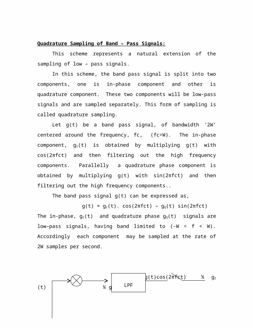
Quadrature Sampling of Band – Pass Signals:
This scheme represents a natural extension of the sampling of low – pass signals.
In this scheme, the band pass signal is split into two components, one is in-phase
component and other is quadrature component. These two components will be low–pass
signals and are sampled separately. This form of sampling is called quadrature sampling.
Let g(t) be a band pass signal, of bandwidth ‘2W’ centered around the frequency,
fc, (fc>W). The in-phase component, gI(t) is obtained by multiplying g(t) with
cos(2πfct) and then filtering out the high frequency components. Parallelly a quadrature
phase component is obtained by multiplying g(t) with sin(2πfct) and then filtering out the
high frequency components..
The band pass signal g(t) can be expressed as,
g(t) = gI(t). cos(2πfct) – gQ(t) sin(2πfct)
The in-phase, gI(t) and quadrature phase gQ(t) signals are low–pass signals, having band
limited to (-W < f < W). Accordingly each component may be sampled at the rate of
2W samples per second.
g(t)cos(2πfct) ½ gI (t) ½ gI (nTs)
sampler
g(t)
cos (2πfct)
g(t) sin(2πfct) ½gQ(t) -½ gQ(nTs)
sampler
sin (2πfct)
Fig 2.8: Generation of in-phase and quadrature phase samples
LPF
LPF
G(f)
-fc 0 fc f
2W->
a) Spectrum of a Band pass signal.
GI(f) / GQ(f)
-W 0 W f
b) Spectrum of gI(t) and gQ(t)
Fig 2.9 a) Spectrum of Band-pass signal g(t)
b) Spectrum of in-phase and quadrature phase signals
RECONSTRUCTION:
From the sampled signals gI(nTs) and gQ(nTs), the signals gI(t) and gQ(t) are
obtained. To reconstruct the original band pass signal, multiply the signals g I(t) by
cos(2πfct) and sin(2πfct) respectively and then add the results.
gI(nTs)
+Cos (2πfct) g(t)
-
gQ(nTs)
Sin (2πfct)
Reconstruction Filter
Σ
Reconstruction Filter
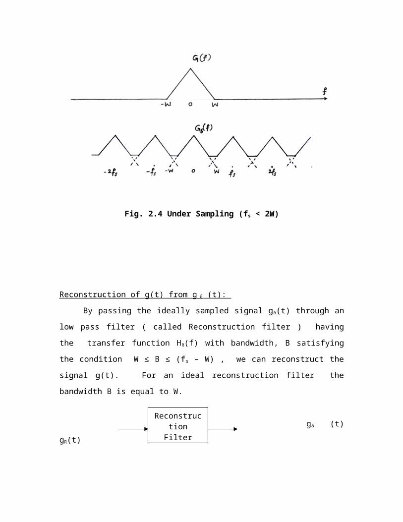
Fig 2.10: Reconstruction of Band-pass signal g(t)

Sample and Hold Circuit for Signal Recovery.
In both the natural sampling and flat-top sampling methods, the spectrum of the signals are scaled by the ratio τ/Ts, where τ is the pulse duration and Ts is the sampling period. Since this ratio is very small, the signal power at the output of the reconstruction filter is correspondingly small. To overcome this problem a sample-and-hold circuit is used .
SW
Input Output g(t) u(t)
a) Sample and Hold Circuit
b) Idealized output waveform of the circuit
Fig: 2.17 Sample Hold Circuit with Waveforms.
The Sample-and-Hold circuit consists of an amplifier of unity gain and low output impedance, a switch and a capacitor; it is assumed that the load impedance is large. The switch is timed to close only for the small duration of each sampling pulse, during which time the capacitor charges up to a voltage level equal to that of the input sample. When the switch is open , the capacitor retains the voltage level until the next closure of the
AMPLIFIER

switch. Thus the sample-and-hold circuit produces an output waveform that represents a staircase interpolation of the original analog signal.The output of a Sample-and-Hold circuit is defined as
where h(t) is the impulse response representing the action of the Sample-and-Hold circuit; that is
h(t) = 1 for 0 < t < Ts0 for t < 0 and t > Ts
Correspondingly, the spectrum for the output of the Sample-and-Hold circuit is given by,
where G(f) is the FT of g(t) and H(f) = Ts Sinc( fTs) exp( -jfTs)
To recover the original signal g(t) without distortion, the output of the Sample-and-Hold circuit is passed through a low-pass filter and an equalizer.
Sampled Analog Waveform Waveform
Fig. 2.18: Components of a scheme for signal reconstruction
Sample and Hold Circuit
Low Pass Filter Equalizer

Signal Distortion in Sampling.
In deriving the sampling theorem for a signal g(t) it is assumed that the signal g(t) is strictly band-limited with no frequency components above ‘W’ Hz. However, a signal cannot be finite in both time and frequency. Therefore the signal g(t) must have infinite duration for its spectrum to be strictly band-limited.
In practice, we have to work with a finite segment of the signal in which case the spectrum cannot be strictly band-limited. Consequently when a signal of finite duration is sampled an error in the reconstruction occurs as a result of the sampling process.
Consider a signal g(t) whose spectrum G(f) decreases with the increasing frequency without limit as shown in the figure 2.19. The spectrum, G(f) of the ideally sampled signal , g(t) is the sum of G(f) and infinite number of frequency shifted replicas of G(f). The replicas of G(f) are shifted in frequency by multiples of sampling frequency, fs. Two replicas of G(f) are shown in the figure 2.19.
The use of a low-pass reconstruction filter with it’s pass band extending from (-fs/2 to +fs/2) no longer yields an undistorted version of the original signal g(t). The portions of the frequency shifted replicas are folded over inside the desired spectrum. Specifically, high frequencies in G(f) are reflected into low frequencies in G(f). The phenomenon of overlapping in the spectrum is called as Aliasing or Foldover Effect. Due to this phenomenon the information is invariably lost.
Fig. 2.19 : a) Spectrum of finite energy signal g(t) b) Spectrum of the ideally sampled signal.

Bound On Aliasing Error:
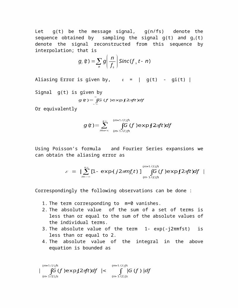
Let g(t) be the message signal, g(n/fs) denote the sequence obtained by sampling the signal g(t) and gi(t) denote the signal reconstructed from this sequence by interpolation; that is
Aliasing Error is given by, = | g(t) - gi(t) |
Signal g(t) is given by
Or equivalently
Using Poisson’s formula and Fourier Series expansions we can obtain the aliasing error as
Correspondingly the following observations can be done :
1. The term corresponding to m=0 vanishes.2. The absolute value of the sum of a set of terms is less than or equal to the sum of
the absolute values of the individual terms.3. The absolute value of the term 1- exp(-j2πmfst) is less than or equal to 2.4. The absolute value of the integral in the above equation is bounded as
Hence the aliasing error is bounded as
Example: Consider a time shifted sinc pulse, g(t) = 2 sinc(2t – 1). If g(t) is sampled at rate of 1sample per second that is at t = 0, ± 1, ±2, ±3 and so on , evaluate the aliasing error.
Solution: The given signal g(t) and it’s spectrum are shown in fig. 2.20.
2.0
1.0
t -1 0 0.5 1 2
-1.0
a) Sinc Pulse
׀G(f)׀
-1.0 -1/2 0 1/2 1.0 f
(b) Amplitude Spectrum, ׀G(f)׀
Fig. 2.20
The sampled signal g(nTs) = 0 for n = 0, ± 1, ±2, ±3 . . . . .and reconstructed signal
gi(t) = 0 for all t.From the figure, the sinc pulse attains it’s maximum value of 2 at time t equal to ½. The aliasing error cannot exceed max|g(t)| = 2.

From the spectrum, the aliasing error is equal to unity.

Natural Sampling:
In this method of sampling, an electronic switch is used to periodically shift
between the two contacts at a rate of fs = (1/Ts ) Hz, staying on the input contact for C
seconds and on the grounded contact for the remainder of each sampling period.
The output xs(t) of the sampler consists of segments of x(t) and hence xs(t) can be
considered as the product of x(t) and sampling function s(t).
xs(t) = x(t) . s(t)
The sampling function s(t) is periodic with period Ts, can be defined as,
S(t) = 1 < t < ------- (1)
Ts/2 > ׀t׀ > 0
Fig: 2.11 Natural Sampling – Simple Circuit.
Fig: 2.12 Natural Sampling – Waveforms.

Using Fourier series, we can rewrite the signal S(t) as
S(t) = Co +
where the Fourier coefficients, Co = / Ts & Cn = fs Sinc(n fs )
Therefore: xs(t) = x(t) [ Co + ]
xs (t) = Co.x(t) +2C1.x(t)cos(wst) + 2C2.x(t)cos (2wst) + . . . . . . . .
Applying Fourier transform for the above equation
FT
Using x(t) X(f)
x(t) cos(2πf0t) ½ [X(f-f0) + X(f+f0)]
Xs(f) = Co.X(f) + C1 [X(f-f0) + X(f+f0)] + C2 [X(f-f0) + X(f+f0)] + ... …
Xs(f) = Co.X(f) +
n≠0
1 X(f)
f -W 0 +W
Message Signal Spectrum Xs(f)
C0
C2 C1 C1 C2
f-2fs -fs -W 0 +W fs 2fs
Sampled Signal Spectrum (fs > 2W)
Fig:2.13 Natural Sampling Spectrum
The signal xs(t) has the spectrum which consists of message spectrum and repetition of
message spectrum periodically in the frequency domain with a period of fs. But the

message term is scaled by ‘Co”. Since the spectrum is not distorted it is possible to
reconstruct x(t) from the sampled waveform xs(t).
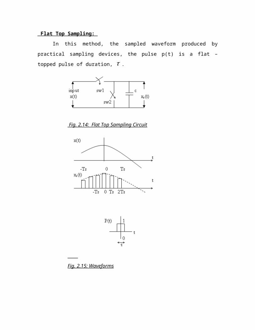
Flat Top Sampling:
In this method, the sampled waveform produced by practical sampling devices,
the pulse p(t) is a flat – topped pulse of duration, .
Fig. 2.14: Flat Top Sampling Circuit
Fig. 2.15: Waveforms
Mathematically we can consider the flat – top sampled signal as equivalent to the
convolved sequence of the pulse signal p(t) and the ideally sampled signal, x δ (t).

xs(t) = p(t) *x δ (t)
xs(t) = p(t) * [ ]
Applying F.T,
Xs(f) = P(f).X δ (f)
= P(f). fs
where P(f) = FT[p(t)] and X δ (f) = FT[x δ (t)]
Aperature Effect:
The sampled signal in the flat top sampling has the attenuated high frequency
components. This effect is called the Aperture Effect.
The aperture effect can be compensated by:
1. Selecting the pulse width as very small.
2. by using an equalizer circuit.
Sampled Signal
Equalizer decreases the effect of the in-band loss of the interpolation filter (lpf).
As the frequency increases, the gain of the equalizer increases. Ideally the amplitude
response of the equalizer is
| Heq(f)| = 1 / | P(f) | =
Low – Pass Filter
EqualizerHeq(f)

Chapter-3
Waveform Coding Techniques
PCM [Pulse Code Modulation]
PCM is an important method of analog –to-digital conversion. In this modulation the analog signal is converted into an electrical waveform of two or more levels. A simple two level waveform is shown in fig 3.1.
Fig:3.1 A simple binary PCM waveform
The PCM system block diagram is shown in fig 3.2. The essential operations in the transmitter of a PCM system are Sampling, Quantizing and Coding. The Quantizing and encoding operations are usually performed by the same circuit, normally referred to as analog to digital converter.
The essential operations in the receiver are regeneration, decoding and demodulation of the quantized samples. Regenerative repeaters are used to reconstruct the transmitted sequence of coded pulses in order to combat the accumulated effects of signal distortion and noise.
PCM Transmitter:
Basic Blocks:1. Anti aliasing Filter2. Sampler3. Quantizer4. Encoder
An anti-aliasing filter is basically a filter used to ensure that the input signal to sampler is free from the unwanted frequency components.For most of the applications these are low-pass filters. It removes the frequency components of the signal which are above the cutoff frequency of the filter. The cutoff frequency of the filter is chosen such it is very close to the highest frequency component of the signal.
Sampler unit samples the input signal and these samples are then fed to the Quantizer which outputs the quantized values for each of the samples. The quantizer output is fed to an encoder which generates the binary code for every sample. The quantizer and encoder together is called as analog to digital converter.
Continuous time message signal PCM Wave
(a) TRANSMITTER
Distorted PCM wave
(b) Transmission Path
Input
(c) RECEIVER
Fig: 3.2 - PCM System : Basic Block Diagram
LPF Sampler Quantizer Encoder
Regeneration Circuit
Decoder Reconstruction Filter
DestinationUser
Regenerative Repeater
Regenerative Repeater

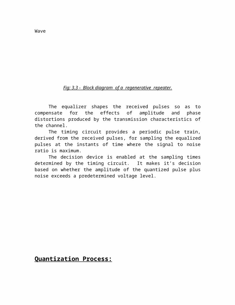
REGENERATIVE REPEATER
REGENERATION: The feature of the PCM systems lies in the ability to control the effects of distortion and noise produced by transmitting a PCM wave through a channel. This is accomplished by reconstructing the PCM wave by means of regenerative repeaters.
Three basic functions: EqualizationTiming and Decision Making
Distorted RegeneratedPCM PCM waveWave
Fig: 3.3 - Block diagram of a regenerative repeater.
The equalizer shapes the received pulses so as to compensate for the effects of amplitude and phase distortions produced by the transmission characteristics of the channel.
The timing circuit provides a periodic pulse train, derived from the received pulses, for sampling the equalized pulses at the instants of time where the signal to noise ratio is maximum.
The decision device is enabled at the sampling times determined by the timing circuit. It makes it’s decision based on whether the amplitude of the quantized pulse plus noise exceeds a predetermined voltage level.
Amplifier - Equalizer
Decision Making Device
Timing Circuit

Quantization Process:
The process of transforming Sampled amplitude values of a message signal into a discrete amplitude value is referred to as Quantization.
The quantization Process has a two-fold effect:1. the peak-to-peak range of the input sample values is subdivided into a finite set
of decision levels or decision thresholds that are aligned with the risers of the staircase, and
2. the output is assigned a discrete value selected from a finite set of representation levels that are aligned with the treads of the staircase..
A quantizer is memory less in that the quantizer output is determined only by the value of a corresponding input sample, independently of earlier analog samples applied to the input.
Fig:3.4 Typical Quantization process.
Types of Quantizers:
1. Uniform Quantizer2. Non- Uniform Quantizer
Ts0 2Ts 3Ts Time
Analog Signal
Discrete Samples( Quantized )

In Uniform type, the quantization levels are uniformly spaced, whereas in non-uniform type the spacing between the levels will be unequal and mostly the relation is logarithmic.
Types of Uniform Quantizers: ( based on I/P - O/P Characteristics)1. Mid-Rise type Quantizer2. Mid-Tread type Quantizer
In the stair case like graph, the origin lies the middle of the tread portion in Mid –Tread type where as the origin lies in the middle of the rise portion in the Mid-Rise type.
Mid – tread type: Quantization levels – odd number. Mid – Rise type: Quantization levels – even number.
Fig:3.5 Input-Output Characteristics of a Mid-Rise type Quantizer
Input
Output
Δ 2Δ 3Δ 4Δ
Δ/2
3Δ/2
5Δ/2
7Δ/2
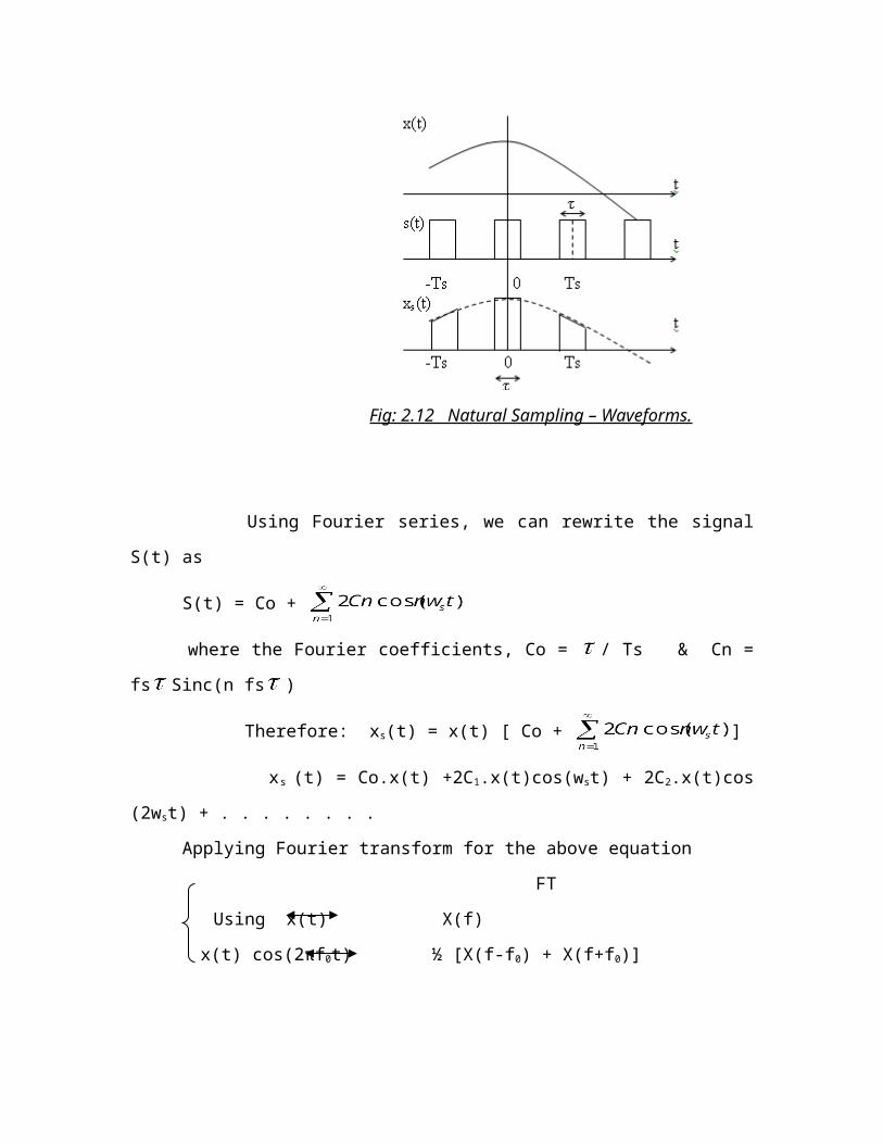
Fig:3.6 Input-Output Characteristics of a Mid-Tread type Quantizer
Quantization Noise and Signal-to-Noise:
“The Quantization process introduces an error defined as the difference between the input signal, x(t) and the output signal, yt). This error is called the Quantization Noise.”
q(t) = x(t) – y(t)
Quantization noise is produced in the transmitter end of a PCM system by rounding off sample values of an analog base-band signal to the nearest permissible representation levels of the quantizer. As such quantization noise differs from channel noise in that it is signal dependent.
Let ‘Δ’ be the step size of a quantizer and L be the total number of quantization levels.Quantization levels are 0, ± Δ., ± 2 Δ., ±3 Δ . . . . . . .
The Quantization error, Q is a random variable and will have its sample values bounded by [-(Δ/2) < q < (Δ/2)]. If Δ is small, the quantization error can be assumed to a uniformly distributed random variable.
Consider a memory less quantizer that is both uniform and symmetric.L = Number of quantization levelsX = Quantizer inputY = Quantizer output
Δ
2Δ
Δ/2
3Δ/2 Input
Output

The output y is given by Y=Q(x) ------------- (3.1)
which is a staircase function that befits the type of mid tread or mid riser quantizer of interest.
Suppose that the input ‘x’ lies inside the interval
Ik = {xk < x ≤ xk+1} k = 1,2,---------L ------- ( 3.2)
where xk and xk+1 are decision thresholds of the interval Ik as shown in figure 3.7.
Fig:3.7 Decision thresholds of the equalizer
Correspondingly, the quantizer output y takes on a discrete value
Y = yk if x lies in the interval Ik
Let q = quantization error with values in the range then
Yk = x+q if ‘n’ lies in the interval Ik
Assuming that the quantizer input ‘n’ is the sample value of a random variable ‘X’ of zero mean with variance .
The quantization noise uniformly distributed through out the signal band, its interfering effect on a signal is similar to that of thermal noise.
Expression for Quantization Noise and SNR in PCM:-
Let Q = Random Variable denotes the Quantization error q = Sampled value of Q
Assuming that the random variable Q is uniformly distributed over the possible range(-Δ/2 to Δ/2) , as
fQ(q) = 1/Δ - Δ/2 ≤ q ≤ Δ/2 ------- (3.3) 0 otherwise
IkIk-1
Xk-1 Xk Xk+1
yk-1 yk
where fQ(q) = probability density function of the Quantization error. If the signal does not overload the Quantizer, then the mean of Quantization error is zero and its variance σQ
2 . fQ(q)
1/Δ
- Δ/2 0 Δ/2 q
Fig:3.8 PDF for Quantization error.
Therefore
---- ( 3.4)
--- (3.5)
Thus the variance of the Quantization noise produced by a Uniform Quantizer, grows as the square of the step size. Equation (3.5) gives an expression for Quantization noise in PCM system.
Let = Variance of the base band signal x(t) at the input of Quantizer.
When the base band signal is reconstructed at the receiver output, we obtain original signal plus Quantization noise. Therefore output signal to Quantization noise ration (SNR) is given by
---------- (3.6)
Smaller the step size Δ, larger will be the SNR.
Signal to Quantization Noise Ratio:- [ Mid Tread Type ]
Let x = Quantizer input, sampled value of random variable X with mean X, variance .
The Quantizer is assumed to be uniform, symmetric and mid tread type.xmax = absolute value of the overload level of the Quantizer.Δ = Step sizeL = No. of Quantization level given by

----- (3.7)
Let n = No. of bits used to represent each level.In general 2n = L, but in the mid tread Quantizer, since the number of representation levels is odd,
L = 2n – 1 --------- (Mid tread only) ---- (3.8)
From the equations 3.7 and 3.8,
Or
---- (3.9)
The ratio is called the loading factor. To avoid significant overload distortion, the
amplitude of the Quantizer input x extend from to , which corresponds to loading factor of 4. Thus with we can write equation (3.9) as
----------(3.10)
-------------(3.11)
For larger value of n (typically n>6), we may approximate the result as
--------------- (3.12)
Hence expressing SNR in db
10 log10 (SNR)O = 6n - 7.2 --------------- (3.13) This formula states that each bit in codeword of a PCM system contributes 6db to the signal to noise ratio. For loading factor of 4, the problem of overload i.e. the problem that the sampled value of signal falls outside the total amplitude range of Quantizer, 8σx is less than 10-4.
The equation 3.11 gives a good description of the noise performance of a PCM system provided that the following conditions are satisfied.
1. The Quantization error is uniformly distributed

2. The system operates with an average signal power above the error threshold so that the effect of channel noise is made negligible and performance is there by limited essentially by Quantization noise alone.
3. The Quantization is fine enough (say n>6) to prevent signal correlated patterns in the Quantization error waveform
4. The Quantizer is aligned with input for a loading factor of 4
Note: 1. Error uniformly distributed2. Average signal power3. n > 64. Loading factor = 4
From (3.13): 10 log10 (SNR)O = 6n – 7.2 In a PCM system, Bandwidth B = nW or [n=B/W] substituting the value of ‘n’ we get
10 log10 (SNR)O = 6(B/W) – 7.2 --------(3.14)
Signal to Quantization Noise Ratio:- [ Mid Rise Type ]
Let x = Quantizer input, sampled value of random variable X with mean X variance .
The Quantizer is assumed to be uniform, symmetric and mid rise type.Let xmax = absolute value of the overload level of the Quantizer.
------------------(3.15)
Since the number of representation levels is even,
L = 2n ------- (Mid rise only) ---- (3.16)
From (3.15) and (3.16)
-------------- (3.17)
-------------(3.18)
where represents the variance or the signal power.
Consider a special case of Sinusoidal signals:

Let the signal power be Ps, then Ps = 0.5 x2max.
-----(3.19)
In decibels, ( SNR )0 = 1.76 + 6.02 n -----------(3.20)
Improvement of SNR can be achieved by increasing the number of bits, n. Thus for ‘n’ number of bits / sample the SNR is given by the above equation 3.19. For every increase of one bit / sample the step size reduces by half. Thus for (n+1) bits the SNR is given by
(SNR) (n+1) bit = (SNR) (n) bit + 6dB
Therefore addition of each bit increases the SNR by 6dB
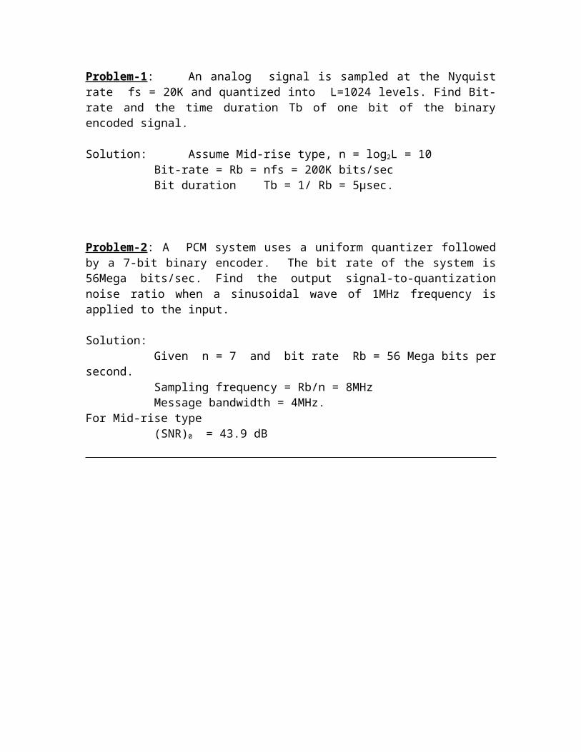
Problem-1: An analog signal is sampled at the Nyquist rate fs = 20K and quantized into L=1024 levels. Find Bit-rate and the time duration Tb of one bit of the binary encoded signal.
Solution: Assume Mid-rise type, n = log2L = 10Bit-rate = Rb = nfs = 200K bits/sec
Bit duration Tb = 1/ Rb = 5µsec.
Problem-2: A PCM system uses a uniform quantizer followed by a 7-bit binary encoder. The bit rate of the system is 56Mega bits/sec. Find the output signal-to-quantization noise ratio when a sinusoidal wave of 1MHz frequency is applied to the input.
Solution: Given n = 7 and bit rate Rb = 56 Mega bits per second.Sampling frequency = Rb/n = 8MHz
Message bandwidth = 4MHz.For Mid-rise type
(SNR)0 = 43.9 dB

CLASSIFICATION OF QUANTIZATION NOISE:The Quantizing noise at the output of the PCM decoder can be categorized into
four types depending on the operating conditions: Overload noise, Random noise, Granular Noise and Hunting noise
OVER LOAD NOISE:- The level of the analog waveform at the input of the PCM encoder needs to be set so that its peak value does not exceed the design peak of Vmax volts. If the peak input does exceed Vmax, then the recovered analog waveform at the output of the PCM system will have flat – top near the peak values. This produces overload noise.
GRANULAR NOISE:- If the input level is reduced to a relatively small value w.r.t to the design level (quantization level), the error values are not same from sample to sample and the noise has a harsh sound resembling gravel being poured into a barrel. This is granular noise.
This noise can be randomized (noise power decreased) by increasing the number of quantization levels i.e.. increasing the PCM bit rate.
HUNTING NOISE:- This occurs when the input analog waveform is nearly constant. For these conditions, the sample values at the Quantizer output can oscillate between two adjacent quantization levels, causing an undesired sinusoidal type tone of frequency (0.5fs) at the output of the PCM system
This noise can be reduced by designing the quantizer so that there is no vertical step at constant value of the inputs.

ROBUST QUANTIZATION
Features of an uniform Quantizer– Variance is valid only if the input signal does not overload Quantizer– SNR Decreases with a decrease in the input power level.
A Quantizer whose SNR remains essentially constant for a wide range of input power levels. A quantizer that satisfies this requirement is said to be robust. The provision for such robust performance necessitates the use of a non-uniform quantizer. In a non-uniform quantizer the step size varies. For smaller amplitude ranges the step size is small and larger amplitude ranges the step size is large.
In Non – Uniform Quantizer the step size varies. The use of a non – uniform quantizer is equivalent to passing the baseband signal through a compressor and then applying the compressed signal to a uniform quantizer. The resultant signal is then transmitted.
Fig: 3.9 MODEL OF NON UNIFORM QUANTIZER
At the receiver, a device with a characteristic complementary to the compressor called Expander is used to restore the signal samples to their correct relative level.
The Compressor and expander take together constitute a Compander.
Compander = Compressor + Expander
Advantages of Non – Uniform Quantization :
1. Higher average signal to quantization noise power ratio than the uniform quantizer when the signal pdf is non uniform which is the case in many practical situation.
2. RMS value of the quantizer noise power of a non – uniform quantizer is substantially proportional to the sampled value and hence the effect of the quantizer noise is reduced.
COMPRESSORUNIFORM
QUANTIZER EXPANDER
Expression for quantization error in non-uniform quantizer:
The Transfer Characteristics of the compressor and expander are denoted by C(x) and C-1(x) respectively, which are related by,
C(x). C-1(x) = 1 ------ ( 3.21 )
The Compressor Characteristics for large L and x inside the interval Ik:
---------- ( 3.22 )
where Δk = Width in the interval Ik.
Let fX(x) be the PDF of ‘X’ . Consider the two assumptions:
– fX(x) is Symmetric– fX(x) is approximately constant in each interval. ie.. fX(x) = fX(yk)
Δk = xk+1 - xk for k = 0, 1, … L-1. ------(3.23) Let pk = Probability of variable X lies in the interval Ik, then
pk = P (xk < X < xk+1) = fX(x) Δk = fX(yk) Δk ------ (3.24)
with the constraint
Let the random variable Q denote the quantization error, then
Q = yk – X for xk < X < xk+1
Variance of Q is σQ
2 = E ( Q2) = E [( X – yk )2 ] ---- (3.25)
---- ( 3.26)
Dividing the region of integration into L intervals and using (3.24)
----- (3.27)
Using yk = 0.5 ( xk + xk+1 ) in 3.27 and carrying out the integration w.r.t x, we obtain that

------- (3.28)
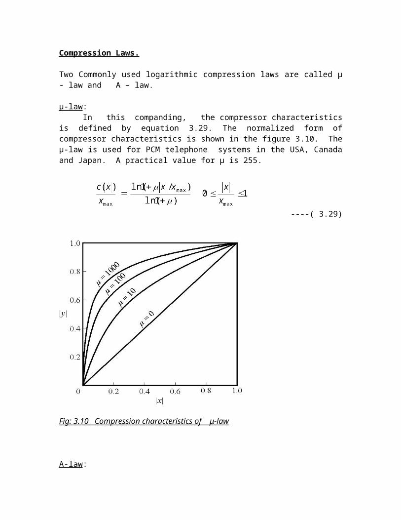
Compression Laws.
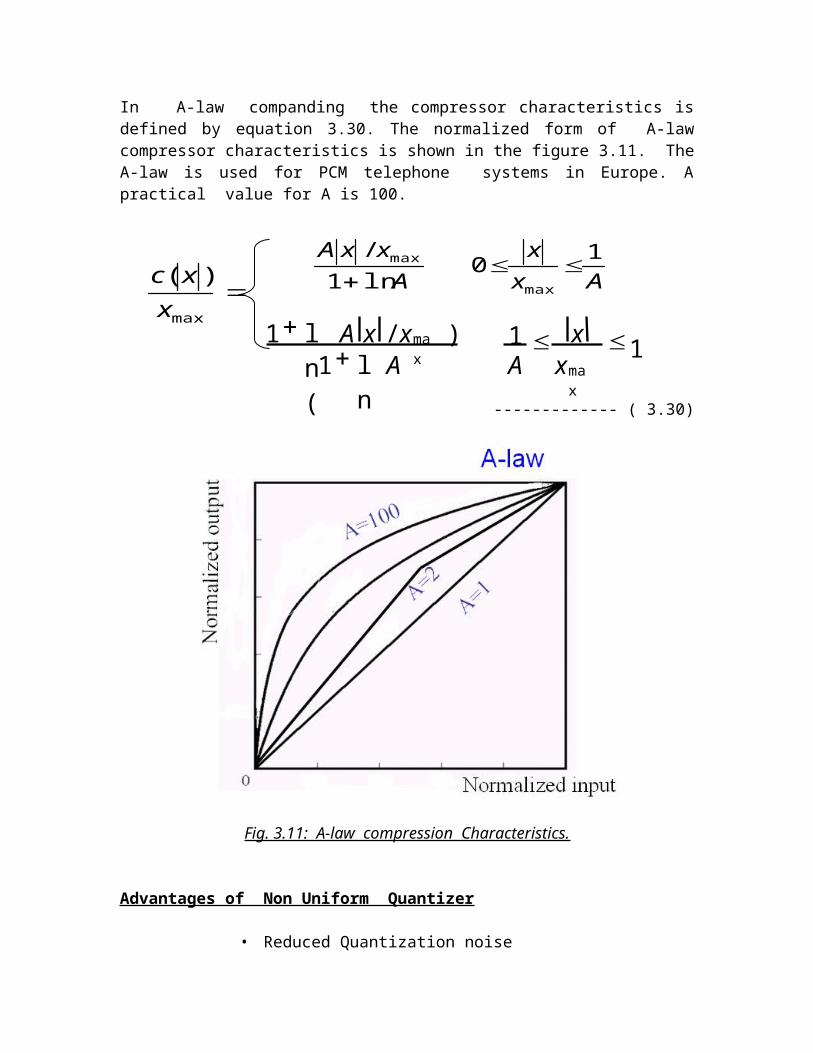
Two Commonly used logarithmic compression laws are called µ - law and A – law.
μ-law:In this companding, the compressor characteristics is defined by equation 3.29.
The normalized form of compressor characteristics is shown in the figure 3.10. The μ-law is used for PCM telephone systems in the USA, Canada and Japan. A practical value for μ is 255.
----( 3.29)
Fig: 3.10 Compression characteristics of μ-law
A-law:

In A-law companding the compressor characteristics is defined by equation 3.30. The normalized form of A-law compressor characteristics is shown in the figure 3.11. The A-law is used for PCM telephone systems in Europe. A practical value for A is 100.
------------- ( 3.30)
Fig. 3.11: A-law compression Characteristics.
Advantages of Non Uniform Quantizer
• Reduced Quantization noise• High average SNR
Differential Pulse Code Modulation (DPCM)
Ax
x
A
xxA 10
ln1
/
max
max
max
)(
x
xc
11ln
1)/ln
(1
max
max
x
xAA
xxA

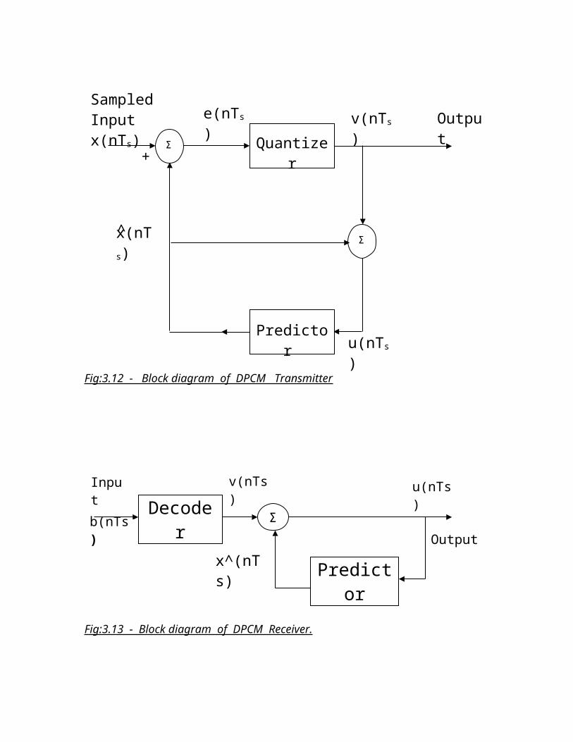
For the signals which does not change rapidly from one sample to next sample, the PCM scheme is not preferred. When such highly correlated samples are encoded the resulting encoded signal contains redundant information. By removing this redundancy before encoding an efficient coded signal can be obtained. One of such scheme is the DPCM technique. By knowing the past behavior of a signal up to a certain point in time, it is possible to make some inference about the future values.
The transmitter and receiver of the DPCM scheme is shown in the fig3.12 and fig 3.13 respectively.
Transmitter: Let x(t) be the signal to be sampled and x(nTs) be it’s samples. In this scheme the input to the quantizer is a signal
e(nTs) = x(nTs) - x^(nTs) ----- (3.31)
where x^(nTs) is the prediction for unquantized sample x(nTs). This predicted value is produced by using a predictor whose input, consists of a quantized versions of the input signal x(nTs). The signal e(nTs) is called the prediction error.
By encoding the quantizer output, in this method, we obtain a modified version of the PCM called differential pulse code modulation (DPCM).
Quantizer output, v(nTs) = Q[e(nTs)] = e(nTs) + q(nTs) ---- (3.32)
where q(nTs) is the quantization error.
Predictor input is the sum of quantizer output and predictor output,
u(nTs) = x^(nTs) + v(nTs) ---- (3.33) Using 3.32 in 3.33, u(nTs) = x^(nTs) + e(nTs) + q(nTs) ----(3.34)
u(nTs) = x(nTs) + q(nTs) ----(3.35)
The receiver consists of a decoder to reconstruct the quantized error signal. The quantized version of the original input is reconstructed from the decoder output using the same predictor as used in the transmitter. In the absence of noise the encoded signal at the receiver input is identical to the encoded signal at the transmitter output. Correspondingly the receive output is equal to u(nTs), which differs from the input x(nts) only by the quantizing error q(nTs).

Fig:3.12 - Block diagram of DPCM Transmitter
Fig:3.13 - Block diagram of DPCM Receiver.
x(nTs)
Sampled Input x(nTs) e(nTs) v(nTs)
Σ Quantizer
Predictor
Σ
+
u(nTs)
Output
^
OutputDecoder Σ
Predictor
Input
b(nTs)
v(nTs) u(nTs)
x^(nTs)

Prediction Gain ( Gp):
The output signal-to-quantization noise ratio of a signal coder is defined as
--------------------( 3.36)
where σx2 is the variance of the signal x(nTs) and σQ
2 is the variance of the quantization error q(nTs). Then
------(3.37)
where σE2 is the variance of the prediction error e(nTs) and (SNR)P is the prediction
error-to-quantization noise ratio, defined by
--------------(3.38)
The Prediction gain Gp is defined as
--------(3.39)
The prediction gain is maximized by minimizing the variance of the prediction error. Hence the main objective of the predictor design is to minimize the variance of the prediction error.
The prediction gain is defined by ---- (3.40)
and ----(3.41) where ρ1 – Autocorrelation function of the message signal
PROBLEM:Consider a DPCM system whose transmitter uses a first-order predictor optimized in the minimum mean-square sense. Calculate the prediction gain of the system for the following values of correlation coefficient for the message signal:
Solution: Using (3.40)
(i) For ρ1= 0.825, Gp = 3.13 In dB , Gp = 5dB
(ii) For ρ2 = 0.95, Gp = 10.26 In dB, Gp = 10.1dB
Delta Modulation (DM)
Delta Modulation is a special case of DPCM. In DPCM scheme if the base band signal is sampled at a rate much higher than the Nyquist rate purposely to increase the

correlation between adjacent samples of the signal, so as to permit the use of a simple quantizing strategy for constructing the encoded signal, Delta modulation (DM) is precisely such as scheme. Delta Modulation is the one-bit (or two-level) versions of DPCM.
DM provides a staircase approximation to the over sampled version of an input base band signal. The difference between the input and the approximation is quantized into only two levels, namely, ±δ corresponding to positive and negative differences, respectively, Thus, if the approximation falls below the signal at any sampling epoch, it is increased by δ. Provided that the signal does not change too rapidly from sample to sample, we find that the stair case approximation remains within ±δ of the input signal. The symbol δ denotes the absolute value of the two representation levels of the one-bit quantizer used in the DM. These two levels are indicated in the transfer characteristic of Fig 3.14. The step size of the quantizer is related to δ by = 2δ ----- (3.42)
Fig-3.14: Input-Output characteristics of the delta modulator.
Let the input signal be x(t) and the staircase approximation to it is u(t). Then, the basic principle of delta modulation may be formalized in the following set of relations:
----- (3.43)
where Ts is the sampling period; e(nTs) is a prediction error representing the difference between the present sample value x(nTs) of the input signal and the latest approximation
Output
Input
+δ
-δ
0

to it, namely .The binary quantity, is the one-bit word transmitted
by the DM system.
The transmitter of DM system is shown in the figure3.15. It consists of a summer, a two-level quantizer, and an accumulator. Then, from the equations of (3.43) we obtain the output as,
----- (3.44)
At each sampling instant, the accumulator increments the approximation to the input signal by ±δ, depending on the binary output of the modulator.
Fig 3.15 - Block diagram for Transmitter of a DM system In the receiver, shown in fig.3.16, the stair case approximation u(t) is reconstructed by passing the incoming sequence of positive and negative pulses through an accumulator in a manner similar to that used in the transmitter. The out-of –band quantization noise in the high frequency staircase waveform u(t) is rejected by passing it through a low-pass filter with a band-width equal to the original signal bandwidth.
Delta modulation offers two unique features:
1. No need for Word Framing because of one-bit code word.2. Simple design for both Transmitter and Receiver
x(nTs)
Sampled Input x(nTs) e(nTs) b(nTs)
Σ One - Bit Quantizer
Delay Ts
Σ
+
u(nTs)
Output
^

Fig 3.16 - Block diagram for Receiver of a DM system
QUANTIZATION NOISE
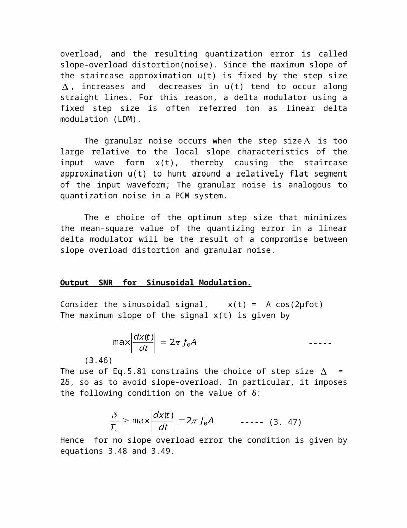
Delta modulation systems are subject to two types of quantization error:(1) slope –overload distortion, and (2) granular noise.
If we consider the maximum slope of the original input waveform x(t), it is clear that in order for the sequence of samples{u(nTs)} to increase as fast as the input sequence of samples {x(nTs)} in a region of maximum slope of x(t), we require that the condition in equation 3.45 be satisfied.
------- ( 3.45 )
Otherwise, we find that the step size = 2δ is too small for the stair case approximation u(t) to follow a steep segment of the input waveform x(t), with the result that u(t) falls behind x(t). This condition is called slope-overload, and the resulting quantization error is called slope-overload distortion(noise). Since the maximum slope of the staircase approximation u(t) is fixed by the step size , increases and decreases in u(t) tend to occur along straight lines. For this reason, a delta modulator using a fixed step size is often referred ton as linear delta modulation (LDM).
The granular noise occurs when the step size is too large relative to the local slope characteristics of the input wave form x(t), thereby causing the staircase approximation u(t) to hunt around a relatively flat segment of the input waveform; The granular noise is analogous to quantization noise in a PCM system.
The e choice of the optimum step size that minimizes the mean-square value of the quantizing error in a linear delta modulator will be the result of a compromise between slope overload distortion and granular noise.
Output SNR for Sinusoidal Modulation.
Low passFilterΣ
DelayTs
Inputb(nTs)
u(nTs)
u(nTs-Ts)

Consider the sinusoidal signal, x(t) = A cos(2µfot)The maximum slope of the signal x(t) is given by
----- (3.46)
The use of Eq.5.81 constrains the choice of step size = 2δ, so as to avoid slope-overload. In particular, it imposes the following condition on the value of δ:
----- (3. 47)
Hence for no slope overload error the condition is given by equations 3.48 and 3.49.
------ (3.48)
------ (3.49)
Hence, the maximum permissible value of the output signal power equals
---- (3.50)
When there is no slope-overload, the maximum quantization error ±δ. Assuming that the quantizing error is uniformly distributed (which is a reasonable approximation for small δ). Considering the probability density function of the quantization error,( defined in equation 3.51 ),
----- (3.51)
The variance of the quantization error is .
----- (3.52)
The receiver contains (at its output end) a low-pass filter whose bandwidth is set equal to the message bandwidth (i.e., highest possible frequency component of the message signal), denoted as W such that f0 ≤ W. Assuming that the average power of the quantization error is uniformly distributed over a frequency interval extending from -1/T s
to 1/Ts, we get the result:
Average output noise power ----- ( 3.53)
Correspondingly, the maximum value of the output signal-to-noise ratio equals

----- (3.54)
Equation 3.54 shows that, under the assumption of no slope-overload distortion, the maximum output signal-to-noise ratio of a delta modulator is proportional to the sampling rate cubed. This indicates a 9db improvement with doubling of the sampling rate.
Problems
1. Determine the output SNR in a DM system for a 1KHz sinusoid sampled at 32KHz without slope overload and followed by a 4KHz post reconstruction filter.
Solution:
Given W=4KHz, f0 = 1KHz , fs = 32KHz Using equation (3.54) we get
(SNR)0 = 311.3 or 24.9dB
Delta Modulation:
Problems
2. Consider a Speech Signal with maximum frequency of 3.4KHz and maximum amplitude of 1volt. This speech signal is applied to a delta modulator whose bit rate is set at 60kbit/sec. Explain the choice of an appropriate step size for the modulator.
Solution: Bandwidth of the signal = 3.4 KHz.Maximum amplitude = 1 voltBit Rate = 60Kbits/secSampling rate = 60K Samples/sec.STEP SIZE = 0.356 Volts
3. Consider a Speech Signal with maximum frequency of 3.4KHz and maximum amplitude of 1volt. This speech signal is applied to a delta modulator whose bit rate is set at 20kbit/sec. Explain the choice of an appropriate step size for the modulator.
Solution: Bandwidth of the signal = 3.4 KHz.
Maximum amplitude = 1 voltBit Rate = 20Kbits/secSampling rate = 20K Samples/sec.STEP SIZE = 1.068 Volts
4. Consider a Delta modulator system designed to operate at 4 times the Nyquist rate for a signal with a 4KHz bandwidth. The step size of the quantizer is 400mV.a) Find the maximum amplitude of a 1KHz input sinusoid for which the delta modulator does not show slope overload.b) Find post-filtered output SNR
Solution: Bandwidth of the signal = f0 =1 KHz.Nyquist Rate = 8K samples/secSampling Rate = 32K samples/sec.Step Size = 400 mV
a) For 1KHz sinusoid, Amax = 2.037 volts.b) Assuming LPF bandwidth = W= 4KHz
SNR = 311.2586 = 24.93 dB
Adaptive Delta Modulation:
The performance of a delta modulator can be improved significantly by making the step size of the modulator assume a time-varying form. In particular, during a steep segment of the input signal the step size is increased. Conversely, when the input signal is varying slowly, the step size is reduced. In this way, the size is adapted to the level of the input signal. The resulting method is called adaptive delta modulation (ADM).
There are several types of ADM, depending on the type of scheme used for adjusting the step size. In this ADM, a discrete set of values is provided for the step size. Fig.3.17 shows the block diagram of the transmitter and receiver of an ADM System. In practical implementations of the system, the step size
or is constrained to lie between minimum and maximum values.
The upper limit, , controls the amount of slope-overload distortion. The lower limit, , controls the amount of idle channel noise. Inside these limits, the adaptation rule
for is expressed in the general form
δ(nTs) = g(nTs). δ(nTs – Ts) ------ (3.55)

where the time-varying multiplier depends on the present binary output of the delta modulator and the M previous values .
This adaptation algorithm is called a constant factor ADM with one-bit memory, where the term “one bit memory” refers to the explicit utilization of the single pervious bit because equation (3.55) can be written as,
g(nTs) = K if b(nTs) = b(nTs – Ts)g(nTs) = K-1 if b(nTs) = b(nTs – Ts) ------ (3.56)
This algorithm of equation (3.56), with K=1.5 has been found to be well matched to typically speech and image inputs alike, for a wide range of bit rates.
Figure: 3.17a) Block Diagram of ADM Transmitter.

Figure: 3.17 b): Block Diagram of ADM Receiver.

Coding Speech at Low Bit Rates:
The use of PCM at the standard rate of 64 kb/s demands a high channel bandwidth for its transmission. But channel bandwidth is at a premium, in which case there is a definite need for speech coding at low bit rates, while maintaining acceptable fidelity or quality of reproduction. The fundamental limits on bit rate suggested by speech perception and information theory show that high quality speech coding is possible at rates considerably less that 64 kb/s (the rate may actually be as low as 2 kb/s).
For coding speech at low bit rates, a waveform coder of prescribed configuration is optimized by exploiting both statistical characterization of speech waveforms and properties of hearing. The design philosophy has two aims in mind:
1. To remove redundancies from the speech signal as far as possible.2. To assign the available bits to code the non-redundant parts of the speech signal in
a perceptually efficient manner.
To reduce the bit rate from 64 kb/s (used in standard PCM) to 32, 16, 8 and 4 kb/s, the algorithms for redundancy removal and bit assignment become increasingly more sophisticated.
There are two schemes for coding speech:1. Adaptive Differential Pulse code Modulation (ADPCM) --- 32 kb/s2. Adaptive Sub-band Coding.--- 16 kb/s
1. Adaptive Differential Pulse – Code Modulation
A digital coding scheme that uses both adaptive quantization and adaptive prediction is called adaptive differential pulse code modulation (ADPCM).
The term “adaptive” means being responsive to changing level and spectrum of the input speech signal. The variation of performance with speakers and speech material, together with variations in signal level inherent in the speech communication process, make the combined use of adaptive quantization and adaptive prediction necessary to achieve best performance.
The term “adaptive quantization” refers to a quantizer that operates with a time-varying step size , where Ts is the sampling period. The step size is varied so as to match the variance of the input signal . In particular, we write
Δ(nTs) = Φ. σ^x(nTs) ----- (3.57)where Φ – Constant
σ^x(nTs) – estimate of the σx(nTs)
Thus the problem of adaptive quantization, according to (3.57) is one of estimating
continuously.

The computation of the estimate in done by one of two ways:
1. Unquantized samples of the input signal are used to derive forward estimates of
- adaptive quantization with forward estimation (AQF)
2. Samples of the quantizer output are used to derive backward estimates of
- adaptive quantization with backward estimation (AQB)
The use of adaptive prediction in ADPCM is required because speech signals are inherently nonstationary, a phenomenon that manifests itself in the fact that autocorrection function and power spectral density of speech signals are time-varying functions of their respective variables. This implies that the design of predictors for such inputs should likewise be time-varying, that is, adaptive. As with adaptive quantization, there are two schemes for performing adaptive prediction:
1. Adaptive prediction with forward estimation (APF), in which unquantized samples of the input signal are used to derive estimates of the predictor coefficients.
2. Adaptive prediction with backward estimation (APB), in which samples of the quantizer output and the prediction error are used to derive estimates of the prediction error are used to derive estimates of the predictor coefficients.
(2) Adaptive Sub-band Coding:
PCM and ADPCM are both time-domain coders in that the speech signal is processed in the time-domain as a single full band signal. Adaptive sub-band coding is a frequency domain coder, in which the speech signal is divided into a number of sub-bands and each one is encoded separately. The coder is capable of digitizing speech at a rate of 16 kb/s with a quality comparable to that of 64 kb/s PCM. To accomplish this performance, it exploits the quasi-periodic nature of voiced speech and a characteristic of the hearing mechanism known as noise masking.
Periodicity of voiced speech manifests itself in the fact that people speak with a characteristic pitch frequency. This periodicity permits pitch prediction, and therefore a further reduction in the level of the prediction error that requires quantization, compared to differential pulse code modulation without pitch prediction. The number of bits per sample that needs to be transmitted is thereby greatly reduced, without a serious degradation in speech quality.
In adaptive sub band coding (ASBC), noise shaping is accomplished by adaptive bit assignment. In particular, the number of bits used to encode each sub-band is varied dynamically and shared with other sub-bands, such that the encoding accuracy is always placed where it is needed in the frequency – domain characterization of the signal. Indeed, sub-bands with little or no energy may not be encoded at all.
Applications
1. Hierarchy of Digital Multiplexers2. Light wave Transmission Link
(1) Digital Multiplexers:
Digital Multiplexers are used to combine digitized voice and video signals as well as digital data into one data stream.
The digitized voice signals, digitized facsimile and television signals and computer outputs are of different rates but using multiplexers it combined into a single data stream.
Fig. 3.18: Conceptual diagram of Multiplexing and Demultiplexing.
Two Major groups of Digital Multiplexers:
1. To combine relatively Low-Speed Digital signals used for voice-grade channels. Modems are required for the implementation of this scheme.
2. Operates at higher bit rates for communication carriers.
Basic Problems associated with Multiplexers:
1. Synchronization.2. Multiplexed signal should include Framing.3. Multiplexer Should be capable handling Small variations
Multiplexer
High-SpeedTransmission
lineDeMux
1
::
::
21
N
2
N
Digital Hierarchy based on T1 carrier:
This was developed by Bell system. The T1 carrier is designed to operate at 1.544 mega bits per second, the T2 at 6.312 megabits per second, the T3 at 44.736 megabits per second, and the T4 at 274.176 mega bits per second. This system is made up of various combinations of lower order T-carrier subsystems. This system is designed to accommodate the transmission of voice signals, Picture phone service and television signals by using PCM and digital signals from data terminal equipment. The structure is shown in the figure 3.19.
Fig. 3.19: Digital hierarchy of a 24 channel system.
The T1 carrier system has been adopted in USA, Canada and Japan. It is designed to accommodate 24 voice signals. The voice signals are filtered with low pass filter having cutoff of 3400 Hz. The filtered signals are sampled at 8KHz. The µ-law Companding technique is used with the constant μ = 255.
With the sampling rate of 8KHz, each frame of the multiplexed signal occupies a period of 125μsec. It consists of 24 8-bit words plus a single bit that is added at the end of the frame for the purpose of synchronization. Hence each frame consists of a total 193 bits. Each frame is of duration 125μsec, correspondingly, the bit rate is 1.544 mega bits per second.

Another type of practical system, that is used in Europe is 32 channel system which is shown in the figure 3.20.
Fig 3.20: 32 channel TDM system
32 channel TDM Hierarchy:
In the first level 2.048 megabits/sec is obtained by multiplexing 32 voice channels. 4 frames of 32 channels = 128 PCM channels, Data rate = 4 x 2.048 Mbit/s = 8.192 Mbit/s, But due to the synchronization bits the data rate increases to 8.448Mbit/sec.
4 x 128 = 512 channels Data rate = 4 x8.192 Mbit/s (+ signalling bits) = 34.368 Mbit/s

(2) Light Wave Transmission
Optical fiber wave guides are very useful as transmission medium. They have a very low transmission losses and high bandwidths which is essential for high-speed communications. Other advantages include small size, light weight and immunity to electromagnetic interference.
The basic optical fiber link is shown in the figure 3.21. The binary data fed into the transmitter input, which emits the pulses of optical power., with each pulse being on or off in accordance with the input data. The choice of the light source determines the optical signal power available for transmission.
Fig: 3.21- Optical fiber link.The on-off light pulses produced by the transmitter are launched into the optical fiber wave guide. During the course of the propagation the light pulse suffers loss or attenuation that increases exponentially with the distance.
At the receiver the original input data are regenerated by performing three basic operations which are :
1. Detection – the light pulses are converted back into pulses of electrical current.2. Pulse Shaping and Timing - This involves amplification, filtering and
equalization of the electrical pulses, as well as the extraction of timing information.
3. Decision Making: Depending the pulse received it should be decided that the received pulse is on or off.
--END—
e-Notes by Prof. H.V.Kumaraswamy, RVCE, Bangalore
CHAPTER 5
Digital modulation techniques
Modulation is defined as the process by which some characteristics of a carrier is
varied in accordance with a modulating wave. In digital communications, the modulating
wave consists of binary data or an M-ary encoded version of it and the carrier is
sinusoidal wave.
Different Shift keying methods that are used in digital modulation techniques are
Amplitude shift keying [ASK]
Frequency shift keying [FSK]
Phase shift keying [PSK]
Fig shows different modulations

1. ASK[Amplitude Shift Keying]:
In a binary ASK system symbol ‘1’ and ‘0’ are transmitted as
tfCosT
EtS
b
b11 2
2)( for symbol 1
0)(2 tS for symbol 0
2. FSK[Frequency Shift Keying]:
In a binary FSK system symbol ‘1’ and ‘0’ are transmitted as
tfCosT
EtS
b
b11 2
2)( for symbol 1
tfCosT
EtS
b
b22 2
2)( for symbol 0
3. PSK[Phase Shift Keying]:

In a binary PSK system the pair of signals S1(t) and S2(t) are used to represent binary symbol ‘1’ and ‘0’ respectively.
tfCosT
EtS c
b
b 22
)(1 --------- for Symbol ‘1’
tfCosT
EtfCos
T
EtS c
b
bc
b
b 22
)2(2
)(2 ------- for Symbol ‘0’
Hierarchy of digital modulation technique
Coherent Binary PSK:
Binary Binary PSK SignalData Sequence
tfCosT
t cb
22
)(1
Fig(a) Block diagram of BPSK transmitter
Non Return to Zero Level
Encoder
Product Modulator
Digital Modulation Technique
Coherent Non - Coherent
Binary (m) = 2
M - ary Hybrid
* ASK M-ary ASK M-ary APK* FSK M-ary FSK M-ary QAM* PSK M-ary PSK
(QPSK)
Binary (m) = 2
M - ary
* ASK M-ary ASK * FSK M-ary FSK * DPSK M-ary DPSK

x(t) x1 Choose 1 if x1>0
Choose 0 if x1<0
Correlator )(1 t Threshold λ = 0
Fig (b) Coherent binary PSK receiver
In a Coherent binary PSK system the pair of signals S1(t) and S2(t) are used to represent
binary symbol ‘1’ and ‘0’ respectively.
tfCosT
EtS c
b
b 22
)(1 --------- for Symbol ‘1’
tfCosT
EtfCos
T
EtS c
b
bc
b
b 22
)2(2
)(2 ------- for Symbol ‘0’
Where Eb= Average energy transmitted per bit 2
10 bbb
EEE
In the case of PSK, there is only one basic function of Unit energy which is given by
bcb
TttfCosT
t 022
)(1
Therefore the transmitted signals are given by
10)()( 11 SymbolforTttEtS bb
00)()( 12 SymbolforTttEtS bb
A Coherent BPSK is characterized by having a signal space that is one dimensional (N=1) with two message points (M=2)
b
T
EdtttSSb
)()( 1
0
111
b
T
EdtttSSb
)()( 1
0
221
Decision Device

The message point corresponding to S1(t) is located at bES 11 and S2(t) is located at
.21 bES
To generate a binary PSK signal we have to represent the input binary sequence in polar
form with symbol ‘1’ and ‘0’ represented by constant amplitude levels of
bb EE & respectively. This signal transmission encoding is performed by a NRZ
level encoder. The resulting binary wave [in polar form] and a sinusoidal carrier )(1 t
[whose frequencyb
cc T
nf ] are applied to a product modulator. The desired BPSK wave
is obtained at the modulator output.
To detect the original binary sequence of 1’s and 0’s we apply the noisy PSK signal x(t)
to a Correlator, which is also supplied with a locally generated coherent reference signal
)(1 t as shown in fig (b). The correlator output x1 is compared with a threshold of zero
volt.
If x1 > 0, the receiver decides in favour of symbol 1.
If x1 < 0, the receiver decides in favour of symbol 0.
Probability of Error Calculation ‘Or’ Bit Error rate Calculation [BER Calculation] :-
In BPSK system the basic function is given by
bcb
TttfCosT
t 022
)(1
The signals S1(t) and S2(t) are given by
10)()( 11 SymbolforTttEtS bb
00)()( 12 SymbolforTttEtS bb
The signal space representation is as shown in fig (N=1 & M=2)
Region R1 Region R2
-

0
Fig. Signal Space Representation of BPSKThe observation vector x1 is related to the received signal x(t) by
dtttxxT
0
11 )()(
If the observation element falls in the region R1, a decision will be made in favour
of symbol ‘1’. If it falls in region R2 a decision will be made in favour of symbol ‘0’.
The error is of two types
1) Pe(0/1) i.e. transmitted as ‘1’ but received as ‘0’ and
2) Pe(1/0) i.e. transmitted as ‘0’ but received as ‘1’.
Error of 1st kind is given by
1
02
21
2 2
)(exp
2
1)0/1( dx
xPe
Assuming Gaussian Distribution
Where μ = mean value = bE for the transmission of symbol ‘0’
2 = Variance = 2
0N for additive white Gaussiance noise.
Threshold Value λ = 0. [Indicates lower limit in integration]
Therefore the above equation becomes
1
0 0
21
0
0
)(exp
1)0/1( dx
N
Ex
NPP b
ee
Put 0
1
N
ExZ b
dzZPPNE
ee
b
)/(
20
0
)(exp1
)0/1(
Message Point 2 S2(t)
Message Point 1 S1(t)Decision
Boundary
02
1)0/1(
N
EerfcP b
e
Similarly 02
1)1/0(
N
EerfcP b
e
The total probability of error )1()1/0()0()0/1( eeeee PPPPP assuming probability of 1’s and 0’s are equal.
)1/0()0/1([2
1eee PPP ]
02
1
N
EerfcP b
e
Coherent Binary FSK
In a binary FSK system symbol ‘1’ and ‘0’ are transmitted as
tfCosT
EtS
b
b11 2
2)( for symbol 1
tfCosT
EtS
b
b22 2
2)( for symbol 0
Frequency b
ci T
inf
for some fixed integer nc and i=1, 2
The basic functions are given by
N
1(k)cR and
OtherwiseZeroandTtfortfCosT
t bb
022
)( 22
Therefore FSK is characterized by two dimensional signal space with two message points i.e. N=2 and m=2.The two message points are defined by the signal vector
01
bES and
bES
02
Generation and Detection:-

fig: FSK transmitter and receiver
A binary FSK Transmitter is as shown in fig. (a). The incoming binary
data sequence is applied to on-off level encoder. The output of encoder is bE volts for
symbol 1 and 0 volts for symbol ‘0’. When we have symbol 1 the upper channel is
switched on with oscillator frequency f1, for symbol ‘0’, because of inverter the lower
channel is switched on with oscillator frequency f2. These two frequencies are combined
using an adder circuit and then transmitted. The transmitted signal is nothing but
required BFSK signal.
The detector consists of two correlators. The incoming noisy BFSK signal x(t) is
common to both correlator. The Coherent reference signal )()( 21 tandt are supplied to
upper and lower correlators respectively.
fig a
fig b

The correlator outputs are then subtracted one from the other and resulting a
random vector ‘l’ (l=x1 - x2). The output ‘l’ is compared with threshold of zero volts.
If l > 0, the receiver decides in favour of symbol 1.
l < 0, the receiver decides in favour of symbol 0.
Probability of Error Calculation:-
In binary FSK system the basic functions are given by
bb
TttfCosT
t 022
)( 11
bb
TttfCosT
t 022
)( 22
The transmitted signals S1(t) and S2(t) are given by
)()( 11 tEtS b for symbol 1
)()( 22 tEtS b for symbol 0
Therefore Binary FSK system has 2 dimensional signal space with two messages S1(t)
and S2(t), [N=2 , m=2] they are represented as shown in fig.
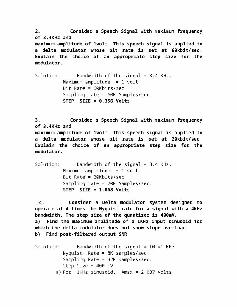
Fig. Signal Space diagram of Coherent binary FSK system.
The two message points are defined by the signal vector
01
bES and
bES
02
The observation vector x1 and x2 ( output of upper and lower correlator) are
related to input signal x(t) as
bT
dtttxx0
11 )()( and
bT
dtttxx0
22 )()(
Assuming zero mean additive white Gaussian noise with input PSD 2
0N. with
variance 2
0N.
The new observation vector ‘l’ is the difference of two random variables x1 & x2.
l = x1 – x2
When symbol ‘1’ was transmitted x1 and x2 has mean value of 0 and bE
respectively.
Therefore the conditional mean of random variable ‘l’ for symbol 1 was
transmitted is
b
b
E
E
xE
xE
lE
0
11121
Similarly for ‘0’ transmission bEl
E
0
The total variance of random variable ‘l’ is given by

0
21 ][][][
N
xVarxVarlVar
The probability of error is given by
dlN
El
NPP b
ee
0 0
2
0
0 2
)(exp
2
1)0/1(
Put 02N
ElZ b
0
2
20
22
1
)exp(1
0
N
Eerfc
dzzP
b
N
E
e
b
Similarly
01 22
1
N
EerfcP b
e
The total probability of error = )1/0()0/1([2
1eee PPP ]
Assuming 1’s & 0’s with equal probabilities
Pe= ][2
110 ee PP
022
1
N
EerfcP b
e
BINARY ASK SYSTEM :-
Binary Binary ASK
Data Sequence Signal
Product Modulator
ON-OFF Level
Encoder

tfCosT
t eb
22
)(1
Fig (a) BASK transmitter
x(t) If x > λ choose symbol 1
If x < λ choose symbol 0
)(1 t Threshold λ
Fig (b) Coherent binary ASK demodulator
In Coherent binary ASK system the basic function is given by
beb
TttfCosT
t 022
)(1
The transmitted signals S1(t) and S2(t) are given by
1)()( 11 SymbolfortEtS b
00)(2 SymbolfortS
The BASK system has one dimensional signal space with two messages (N=1, M=2)
bE
)(1 t
0 2
bE
Fig. (c) Signal Space representation of BASK signal
In transmitter the binary data sequence is given to an on-off encoder. Which
gives an output bE volts for symbol 1 and 0 volt for symbol 0. The resulting binary
Decision Device X
bT
dt0
Region E1 Region E2
Message Point 2
Message Point 1

wave [in unipolar form] and sinusoidal carrier )(1 t are applied to a product modulator.
The desired BASK wave is obtained at the modulator output.
In demodulator, the received noisy BASK signal x(t) is apply to correlator with
coherent reference signal )(1 t as shown in fig. (b). The correlator output x is compared
with threshold λ.
If x > λ the receiver decides in favour of symbol 1.
If x < λ the receiver decides in favour of symbol 0.
BER Calculation:
In binary ASK system the basic function is given by
bcb
TttfCosT
t 022
)(1
The transmitted signals are given by
1)()( 11 SymbolfortEtS b
00)(2 SymbolfortS
Therefore the average transmitted energy per bit 42
20
2
2
2
10 b
b
bbb
TATA
EEE
The probability of error is given by
dxN
x
NP
bE oe
2
2
0
0
)0(exp
1
Where ‘x’ is the observed random vector. μ = 0, because the average value for symbol ‘0’
transmission is zero (0).
202 N
assuming additive white Gaussian noise with into PSD 2
0N
Let 0N
xZ
0
2
20
22
1
)exp(1
0
N
Eerfc
dzzP
b
N
E
e
b
similarly
01 22
1
N
EerfcP b
e
The total probability of error = ][2
110 ee PP
022
1
N
EerfcP b
e
Incoherent detection :
Fig(a). : Envelope detector for OOK BASK

Incoherent detection as used in analog communication does not require carrier for
reconstruction. The simplest form of incoherent detector is the envelope detector as
shown in figure(a). The output of envelope detector is the baseband signal. Once the
baseband signal is recovered, its samples are taken at regular intervals and compared with
threshold.
If Z(t) is greater than threshold ( ) a decision will be made in favour of symbol ‘1’
If Z(t) the sampled value is less than threshold ( ) a decision will be made in favour of
symbol ‘0’.
Non- Coherenent FSK Demodulation:-
Fig(b) : Incoherent detection of FSK
Fig(b) shows the block diagram of incoherent type FSK demodulator. The detector
consists of two band pass filters one tuned to each of the two frequencies used to
communicate ‘0’s and ‘1’s., The output of filter is envelope detected and then baseband
detected using an integrate and dump operation. The detector is simply evaluating which
of two possible sinusoids is stronger at the receiver. If we take the difference of the
outputs of the two envelope detectors the result is bipolar baseband.
The resulting envelope detector outputs are sampled at t = kTb and their values are
compared with the threshold and a decision will be made infavour of symbol 1 or 0.
Differential Phase Shift Keying:- [DPSK]
Fig. (a) DPSK Transmitter
Fig. (b) DPSK Receiver
A DPSK system may be viewed as the non coherent version of the PSK. It eliminates
the need for coherent reference signal at the receiver by combining two basic operations
at the transmitter
(1) Differential encoding of the input binary wave and
(2) Phase shift keying
Hence the name differential phase shift keying [DPSK]. To send symbol ‘0’ we
phase advance the current signal waveform by 1800 and to send symbol 1 we leave the
phase of the current signal waveform unchanged.
The differential encoding process at the transmitter input starts with an arbitrary
first but, securing as reference and thereafter the differentially encoded sequence{dk} is
generated by using the logical equation.
bdbdd kkkkk 11
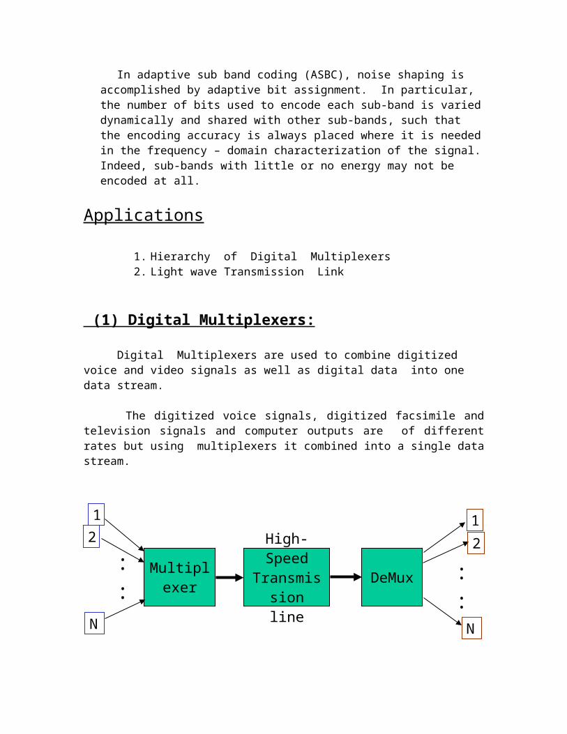
Where bk is the input binary digit at time kTb and dk-1 is the previous value of the
differentially encoded digit. Table illustrate the logical operation involved in the
generation of DPSK signal.
Input Binary Sequence {bK} 1 0 0 1 0 0 1 1
Differentially Encoded 1
sequence {dK}
1 0 1 1 0 1 1 1
Transmitted Phase 0 0 Π 0 0 Π 0 0 0
Received Sequence
(Demodulated Sequence)
1 0 0 1 0 0 1 1
A DPSK demodulator is as shown in fig(b). The received signal is first passed
through a BPF centered at carrier frequency fc to limit noise power. The filter output and
its delay version are applied to correlator the resulting output of correlator is proportional
to the cosine of the difference between the carrier phase angles in the two correlator
inputs. The correlator output is finally compared with threshold of ‘0’ volts .
If correlator output is +ve -- A decision is made in favour of symbol ‘1’
If correlator output is -ve --- A decision is made in favour of symbol ‘0’
COHERENT QUADRIPHASE – SHIFT KEYING
Fig. (a) QPSK Transmitter
Fig. (b) QPSK Receiver
In case of QPSK the carrier is given by
410)2sin(]4/)12sin[(2
)2cos(]4/)12[(2
)(
410]4/)12(2[2
)(
toiTttfiT
EtfiCos
T
Ets
toiTtitfCosT
Ets
cci
ci

Fig. (c) QPSK Waveform
In QPSK system the information carried by the transmitted signal is contained in
the phase. The transmitted signals are given by
114
72cos
2)(
014
52cos
2)(
004
32cos
2)(
104
2cos2
)(
3
2
1
dibitinputfortT
Et
dibitinputfortT
Et
dibitinputfortT
Et
bitdiinputfortT
Et
fS
fS
fS
fS
ct
c
c
c
Where the carrier frequency 7nf C
C for some fixed integer nc

E = the transmitted signal energy per symbol.
T = Symbol duration.
The basic functions bygivenaretandt )()(21
Tttt
Tttt
fT
fT
cb
cb
02sin2
)(
02cos2
)(
2
1
There are four message points and the associated signal vectors are defined by
4,3,2,1
412sin
412cos
i
iE
iE
Si
The table shows the elements of signal vectors, namely Si1 & Si2
Table:-
Input dibit
Phase of
QPSK
signal(radians)
Coordinates of message
points
Si1 Si2
104
2
E 2E
004
32
E 2E
014
52
E 2E
114
72
E 2E

Therefore a QPSK signal is characterized by having a two dimensional signal
constellation(i.e.N=2)and four message points(i.e. M=4) as illustrated in fig(d)
.Fig (d) Signal-space diagram of coherent QPSK system.
Generation:-
Fig(a) shows a block diagram of a typical QPSK transmitter, the incoming binary
data sequence is first transformed into polar form by a NRZ level encoder. Thus the
symbols 1& 0 are represented by EE bband respectively. This binary wave is
next divided by means of a demultiplexer [Serial to parallel conversion] into two separate
binary waves consisting of the odd and even numbered input bits. These two binary
waves are denoted by ao(t) and ae(t)
The two binary waves ao(t) and ae(t) are used to modulate a pair of quadrature
carriers or orthonormal basis functions )(&)(21
tt which are given by
tT
t
tT
t
f
f
c
c
2sin2
)(
&
2cos2
)(
2
1
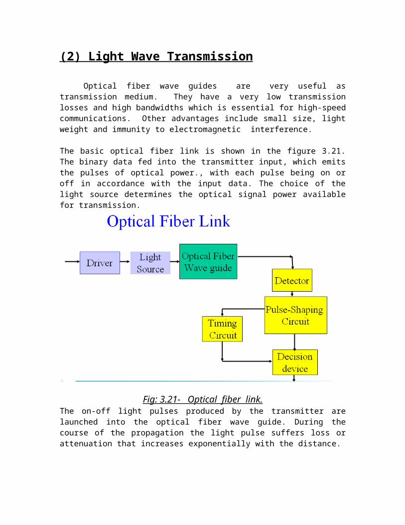
The result is a pair of binary PSK signals, which may be detected independently due to
the orthogonality of )(&)(21
tt .
Finally the two binary PSK signals are added to produce the desired QPSK signal.
Detection:-
The QPSK receiver consists of a pair of correlators with a common input and supplied
with a locally generated pair of coherent reference signals )(&)(21
tt as shown in
fig(b).The correlator outputs x1 and x2 produced in response to the received signal x(t) are
each compared with a threshold value of zero.
The in-phase channel output :
If x1 > 0 a decision is made in favour of symbol 1
x1 < 0 a decision is made in favour of symbol 0
Similarly quadrature channel output:
If x2 >0 a decision is made in favour of symbol 1 and
x2 <0 a decision is made in favour of symbol 0
Finally these two binary sequences at the in phase and quadrature channel outputs are
combined in a multiplexer (Parallel to Serial) to reproduce the original binary sequence.
Probability of error:-
A QPSK system is in fact equivalent to two coherent binary PSK systems
working in parallel and using carriers that are in-phase and quadrature.
The in-phase channel output x1 and the Q-channel output x2 may be viewed as the
individual outputs of the two coherent binary PSK systems. Thus the two binary PSK
systems may be characterized as follows.
- The signal energy per bit 2E
- The noise spectral density is 2
0N
The average probability of bit error in each channel of the coherent QPSK system is

N
N
Eerfc
EEE
erfcP
2 0
0
1
2
1
22
2
1
The bit errors in the I-channel and Q-channel of the QPSK system are statistically
independent . The I-channel makes a decision on one of the two bits constituting a
symbol (di bit) of the QPSK signal and the Q-channel takes care of the other bit.
Therefore, the average probability of a direct decision resulting from the
combined action of the two channels working together is
pc= probability of correct reception
p1= probability of error
No
Eerfc
No
Eerfc
No
Eerfc
PPC
24
1
21
22
11
1
2
2
21
The average probability of symbol error for coherent QPSK is given by
No
Eerfc
No
Eerfc
PP Ce
24
1
2
1
2
In the region where 12
oN
E We may ignore the second term and so the
approximate formula for the average probability of symbol error for coherent QPSK
system is
No
EerfcPe 2
Minimum shift keying:-

In a continuous phase frequency shift keying [CPFSK] system the transmitted
signal is given by
0)0(2cos2
1)0(2cos2
)(
2
1
symbolfort
symbolfort
tS
fTE
fTE
b
b
b
b
Where Eb is the transmitted signal energy per bit and Tb is bit duration the CPSK signal
S(t) is expressed in the conventional form of an angle modulated signal as
)0(2cos2
)( ttS fTE
cb
b
The phase θ(t) is a continuous function of time which is given by
ratiodeviationtheh
frequencycarriertheWhere
Th
h
h
bygivenaresfrequenciedtransmitteThe
tt
t
fff
fffT
ff
Tff
ff
TTh
c
b
c
bc
bc
bb
&
)(
)(2/1
&
0)0()(
21
21
2
1
21
2
2
The variation of phase θ(t) with time t follows a path consisting of sequence of straight
lines, the slope of which represent frequency change Fig(a) shows the possible paths
starting from time t=0. This plot is known as “Phase tree”.
When h= ½ the frequency deviation equals half the bit rate. This is the minimum
frequency difference (deviation) that allows the two FSK signals representing symbol ‘1’
& ‘0’. For this reason a CPFSK signal with a deviation ratio of one- half is commonly
referred to as “minimum shift keying”[MSK].

Deviation ratio h is measured with respect to the bit rate 1/Tb
at t =Tb
fig(b) phase tree
Fig(c): Phase Trellis, for sequence 1101000
In terms of In phase and Quadrature Component

with the deviation ratio h=1/2
+ Sign corresponds to symbol 1
- Sign corresponds to symbol 0
In phase components
For the interval of
consists of half cosine pulse
+ Sign corresponds to θ(0) =0
- Sign corresponds to θ(0) = п
Quadrature components
For the interval of
consists of half sine pulse
+ Sign corresponds to θ(Tb) =п/2
- Sign corresponds to θ(Tb) = -п/2
since the phase states θ(0) and θ(Tb) can each assume one of the two possible values,
any one of the four possibilities can arise

Basic functions are given by
we may express the MSK signal in the form
The coefficients are given by
and
The signal space diagram for MSK system is as shown in fig

Fig: signal space diagram for MSK system
Signal Space Characterization of MSK

Fig: sequence and waveforms for MSK signal
(a) input binary sequence (b) scaled time function )(11 ts
(c) scaled time function )(22 ts (d)obtained by adding (b) and (c)
In the case of AWGN channel, the received signal is given by
x(t) = s(t) + w(t)
where s(t) is the transmitted MSK signal and w(t) is the sample function of a white
Gaussian noise.
The projection of the received signal x(t) onto the reference signal )(1 t is
similarly the projection of the received signal x(t) onto the reference signal )(2 t is
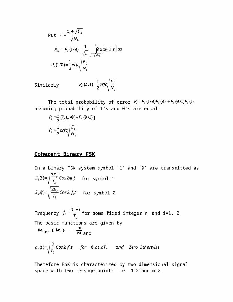
If x2>0, the receiver chooses the estimate 2
)(^ bT . If, on the other hand, x2<0, it
chooses the estimate 2
)(^ bT .
To reconstruct the original binary sequence, we interleave the above two sets of phase decisions,
1 If we have the estimates 0)0(^
and 2
)(^ bT , or alternatively if we have the
estimates )0(^
and 2
)(^ bT , the receiver makes a final decision in favor of
symbol 0.
2 If we have the estimates )0(^
and 2
)(^ bT , or alternatively if we have
the estimates 0)0(^
and 2
)(^ bT , the receiver makes a final decision in favor of
symbol 1.
Generation and detection of MSK signal:-

Fig. (b) MSK Receiver
Fig (a) shows the block diagram of typical MSK transmitter. and (b)receiver
Two input sinusoidal waves one of frequency Tn
b
C
4f c for some fixed integer nc and
the other of frequency T b41
are first applied to a modulator. This produces two phase
coherent sinusoidal waves at frequencies f1 and f2 which are related to the carrier
frequency fc and the bit rate Rb by
2
1
2
2
2
2
2
1
hforh
orh
hor
h
RfT
ff
RfT
ff
bCb
c
bCb
c
These two sinusoidal waves are separated from each other by two narrow band filters one
centered at f1 and the other at f2. The resulting filter outputs are next linearly combined to
produce the pair of basis functions )()(21
tandt . Finally )()(21
tandt are
multiplied with two binary waves a1(t) and a2(t) both of which have a bit rate equal
to T b21
. These two binary waves are extracted from the incoming binary sequence.

Fig (b) shows the block diagram of a typical MSK receiver. The received signal
x(t) is correlated with locally generated replicas of the coherent reference signals
)()(21
tandt . The integration in the Q – channel is delayed by Tb seconds with
respect to the I - channel.
The resulting in-phase and quadrature channel correlator outputs x1 and x2 are
each compared with a threshold of zero. To estimate the phase θ(0) and θ(T b). Finally
these phase decisions are interleaved so as to reconstruct the original input binary
sequence with a minimum average probability of symbol error in an AGWN channel.
PROBLEM 1.

Binary data has to be transmitted over a telephone link that has a usable bandwidth of
3000Hz and a maximum achievable signal-to-noise power ratio of 6 dB at its output..
a. Determine the maximum signaling rate and probability of error if a coherent
ASK scheme is used for transmitting binary data through this channel.
b. If the data is maintained at 300 bits/sec, calculate the error probability.
Solution:
a) If we assume that an ASK signal requires a bandwidth of 3rb Hz, then the
maximum signaling rate permissible is given by
Bandwidth =3 rb=3000 Hz
rb=1000 bits/sec.
0003.0464.312
124,
000,48
000,124
300022
4
2
2
2
2
QQP
andrAHence
A
A
PowerNoise
PowerSignalAverage
PowerNoise
APowerSignalAverage
e
b
b) If the bit rate is reduced to 300 bits/sec, then
10
2
10326.640
404
QQPe
r
A
b
PROBLEM 2

Binary data is transmitted over an RF band pass channel with a usable bandwidth of
10 MHz at a rate of (4.8) (106) bits/sec using an ASK signaling method. The carrier
amplitude at the receiver antenna is 1 mv and the noise power spectral density at the
receiver input is 10-15 watt/Hz. Find the error probability of a coherent and non coherent
receiver..
Solution:
a) The bit error probability for the coherent demodulator is
).10(226
/102/
8.4/10,1;4
7
15
62
QPe
Hzwatt
TmvATA
QP bb
e
b) for non coherent ASK pe is given by
,)16/(exp2
1 2 be TAP
pe = 0.0008
PROBLEM 3.
Binary data is transmitted at a rate of 106 bits/sec over a microwave link having a
bandwidth of 3 MHz. Assume that the noise power spectral density at the receiver input
is ./102/ 10 Hzwatt Find the average carrier power required at the receiver input for
coherent PSK and DPSK signaling schemes to maintain Pe ≤10-4.
Solution:
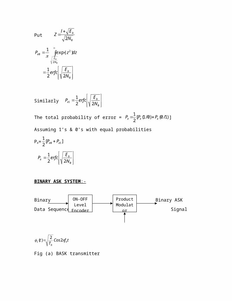
The probability of error for the PSK scheme is
dBmS
TS
Hence
TAP
schemeDPSKtheFor
dBmS
TS
thus
TSQP
DPSKav
bav
bDPSKe
av
bav
bavPSKe
3.3.2
517.8/
,
,102/exp2
1
48.1)10()10()75.3()(
75.3/2
,10/2
42
6102
4
This example illustrates that the DPSK signaling scheme requires about 1 dB more power
than the coherent PSK scheme when the error probability is of the order of
10-4.
Probability of Error

Definition: Defines average probability of error that can occur in a Communication
system
Error Functions(1) Error function erf(u):
u
dzzuerf0
2 )exp(2
)(
-------- ( A6.1)
(2) Complementary error function erfc(u):
u
dzzuerfc )exp(2
)( 2
-------- ( A6.2)
Properties of Error function
1. erf(-u) = -erf(u) - Symmetry.
2. erf(u) approaches unity as u tends towards infinity.
1)exp(2
0
2
dzz
-------- ( A6.3)
3. For a Random variable X, with mean mx and variance σx2, the probability
of X is defined by
X
XX
aerfamXamP
2)( -------- ( A6.4)
Note: Relation: erfc(u) = 1 – erf(u)Tables are used to find these values.
Approximate Relation: ( only for large values of u )
)exp(
)(2u
uerfc
-------- ( A6.5)
Q – Function:

An alternate form of error function. It basically defines the area under the Standardized
Gaussian tail. For a standardized Gaussian random variable X of zero mean and unit
variance, the Q-function is defined by
dxx
vQv
2exp
2
1)(
2
-------- ( A6.6)
Relations between Q-function and erfc function:
(i)
22
1)(
verfcvQ ------- ( A6.7a)
(ii) )2(2 uQuerfc ------ ( A6.7b)

Probability of Error Calculation for Binary PCM Systems
Consider a binary communication system in which the two symbols binary1 and binary0
are represented by the signals s1(t) and s2(t) respectively. Let E1 and E2 represent the
energies of the signals s1(t) and s2(t) respectively.
dttsETb
0
211 )( and dttsE
Tb
0
222 )( ----- ( A6.8)
The Probability of error for Communication Systems can be defined as
02
)1(
2
1
N
EerfcP b
e
--------- ( A6.9)
Where Eb is the average energy per bit defined by
221 EE
Eb
--------- ( A6.10)
and ρ is the correlation coefficient
dttstsE
Tb
b0
21 )()(1 ------ ( A6.11)
and (No/2) represent the noise power spectral density in W/Hz.
Case (1): Uni-polar signaling:
In this scheme the signals are represented as
10)(1 SymbolforTtatS b
000)(2 SymbolforTttS b

Signal energies are E1 = a2 Tb and E2 = 0
Average energy per bit, Eb = a2 Tb/2.
Correlation coefficient = 0.
Probability of error,
02
)1(
2
1
N
EerfcP b
e
0
2
42
1
N
TaerfcP b
e
Case (2): Polar signaling:
In this scheme the signals are represented as
10)(1 SymbolforTtatS b
00)(2 SymbolforTtatS b

Signal energies are E1 = a2 Tb and E2 = a2 Tb
Average energy per bit, Eb = a2 Tb
Correlation coefficient = -1.
Probability of error,
02
)1(
2
1
N
EerfcP b
e
0
2
2
1
N
TaerfcP b
e
Case (3): Manchester signaling:
In this scheme the signals are represented as
bb
b
TtTa
SymbolforTtatS
2/2/
12/02/)(1
bb
b
TtTa
SymbolforTtatS
2/2/
02/02/)(2
Signal energies are E1 = a2 Tb/4 and E2 = a2 Tb/4
Average energy per bit, Eb = a2 Tb/4
Correlation coefficient = -1.
Probability of error,
02
)1(
2
1
N
EerfcP b
e
Reduces to
0
2
42
1
N
TaerfcP b
e

Example:
A binary PCM system using NRZ signaling operates just above the error threshold
with an average probability of error equal to 10-6. If the signaling rate is doubled,
find the new value of the average probability of error.
Solution:
For probability of error equal to 10-6.
Eb/N0 = 3.3 (from table)
The probability of error is
02
1
N
EerfcP b
e
If the signaling rate is doubled then Eb is reduced by a factor of 2 and correspondingly
Eb/N0 also reduces by 2. Hence the new probability of error will become .
310eP

Chapter 6
DETECTION AND ESTIMATION:
Fundamental issues in digital communications are
1. Detection and2. Estimation
Detection theory: It deals with the design and evaluation of decision – making processor that observes the received signal and guesses which particular symbol was transmitted according to some set of rules.
Estimation Theory: It deals with the design and evaluation of a processor that uses information in the received signal to extract estimates of physical parameters or waveforms of interest. The results of detection and estimation are always subject to errors
Model of digital communication system
Consider a source that emits one symbol every T seconds, with the symbols belonging to an alphabet of M symbols which we denote as m1, m2, . . . . . . mM.We assume that all M symbols of the alphabet are equally likely. Then
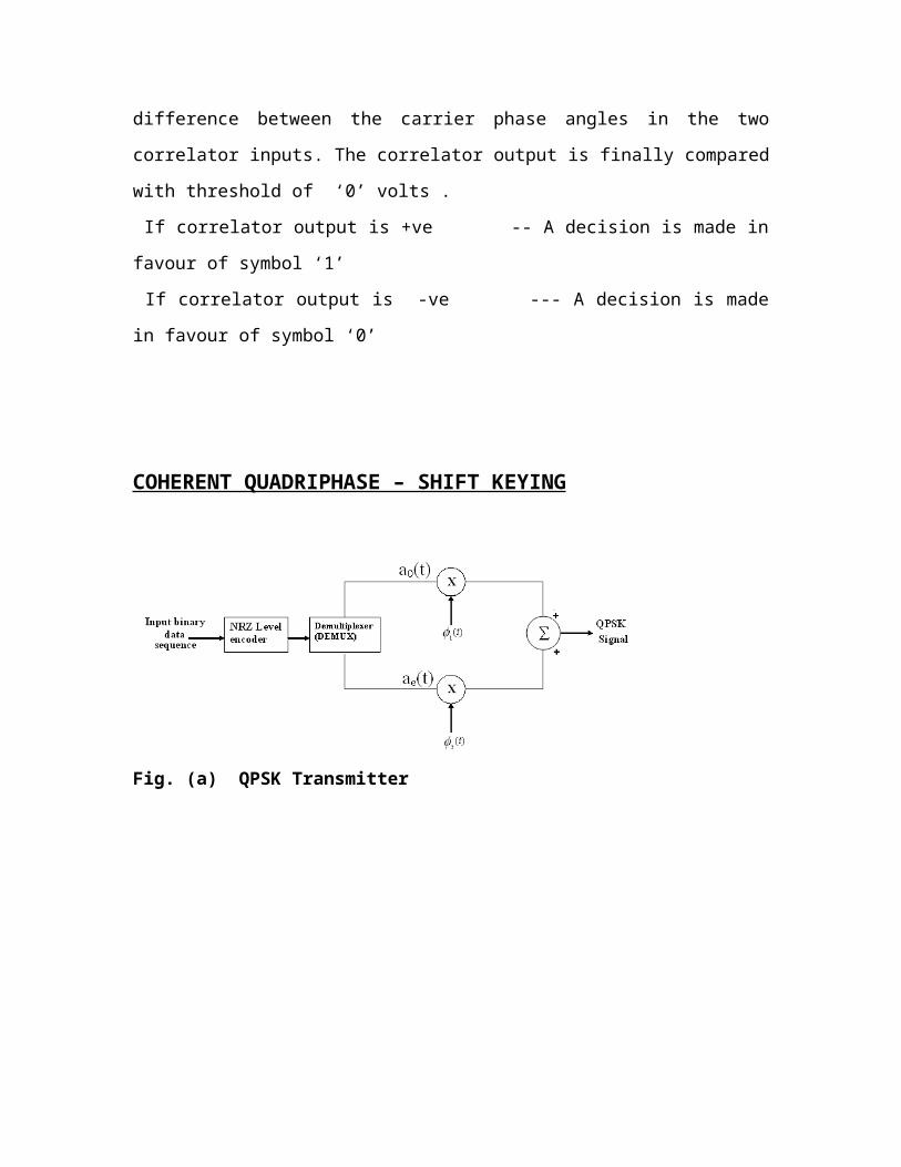
The output of the message source is presented to a vector transmitter producing vector of real number
Where the dimension N ≤ M.
The modulator then constructs a distinct signal si(t) of duration T seconds. The signal si(t) is necessarily of finite energy.
The Channel is assumed to have two characteristics: Channel is linear, with a bandwidth that is large enough to accommodate
the transmission of the modulator output si(t) without distortion. The transmitted signal si(t) is perturbed by an additive, zero-mean,
stationary, white, Gaussian noise process.such a channel is referred as AWGN ( additive white Gaussian noise ) channel
GRAM – SCHMIDT ORTHOGONALIZATION PROCEDURE:
In case of Gram-Schmidt Orthogonalization procedure, any set of ‘M’ energy signals {Si(t)} can be represented by a linear combination of ‘N’ orthonormal basis functions where N≤M. That is we may represent the given set of real valued energy signals S1(t), S2(t). . . . . . . SM(t) each of duration T seconds in the form
)(........)()()( 12121111 tStStStS NN )(........)()()( 22221212 tStStStS NN
.
.
.
.
)(........)()()( 2211 tStStStS NMNMMM
)1.6(......3,2,1
0)()(
1 Mi
TttStS
N
jjiji
Where the Co-efficient of expansion are defined by

)2.6(......3,2,1
.....3,2,1)()()(
0 Nj
MidtttStS
T
jiij
The basic functions )(.........)(),( 21 ttt N are orthonormal by which
)3.6(0
1)()(
0 jiif
jiifdttt
T
ji
The co-efficient Sij may be viewed as the jth element of the N – dimensional Vector Si
Therefore
iN
i
i
i
S
S
S
S
'
'
'
'2
1
i = 1,2,3 . . . . . . M
Let
Vector
Geometric interpretation of signal:
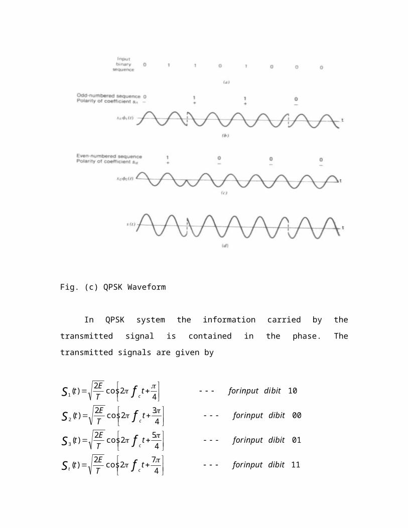
Using N orthonormal basis functions we can represent M signals as
Coefficients are given by
Given the set of coefficients {sij}, j= 1, 2, ….N operating as input we may use the scheme as shown in fig(a) to generate the signal si(t) i = 1 to M. It consists of a bank of N multipliers, with each multiplier supplied with its own basic function, followed by a summer.
conversely given a set of signals si(t) i = 1 to M operating as input we may use the scheme shown in fig (b) to calculate the set of coefficients {sij}, j= 1, 2, ….N
fig(a)

The vector si is called signal vector
We may visualize signal vectors as a set of M points in an N dimensional Euclidean space, which is also called signal spaceThe squared-length of any vector si is given by inner product or the dot product of si
Where sij are the elements of si
Two vectors are orthogonal if their inner product is zero
The energy of the signal is given by
substituting the value si(t) from equation 6.1
interchanging the order of summation and integration
fig(b)

since )(tj forms an orthonormal set, the above equation reduce to
this shows that the energy of the signal si(t) is equal to the squared-length of the signal vector si
The Euclidean distance between the points represented by the signal vectors si and sk is
Response of bank of correlators to noisy input
Received Signal X(t) is given by
where W(t) is AWGN with Zero Mean and PSD N0/2Output of each correlator is a random variable defined by
The first Component Sij is deterministic quantity contributed by the transmitted signal Si(t), it is defined by
The second Component Wj is a random variable due to the presence of the noise at the input, it is defined by

let )(' tX is a new random variable defined as
substituting the values of X(t) from 6.6 and Xj from 6.7 we get
which depends only on noise W(t) at the front end of the receiver and not at all on the transmitted signal si(t). Thus we may express the received random process as
Now we may characterize the set of correlator output, {Xj}, j = 1 to N , since the received random process X(t) is Gaussian , we deduce that each Xj is a Gaussian random variable. Hence, each Xj is characterized completely by its mean and variance.
Mean and variance:The noise process W(t) has zero mean, hence the random variable Wj extracted from W(t) also has zero mean. Thus the mean value of he jth correlator output depends only on Sij as
variance of Xj is given by

substituting the value of Wj from eqn 6.9
where
= ])()([ uWtWE autocorrelation function of the noise process W(t).Science the noise is stationary, with psd N0/2 ,Rw(t,u) depends only on the time difference (t-u) and expressed as
substituting this value in the equation 6.11 we get
Science the )(tj have unit energy, the above equation reduce to
This shows that all the correlator outputs {Xj}, j = 1 to N have a variance equal to the psd No/2 of the additive noise process W(t). Science the )(tj forms an orthogonal set, then the Xj are mutually uncorrelated, as shown by

Since the Xj are Gaussian random variables, from the above equation it is implied that they are also statistically independent.
Detection of known signals in noiseAssume that in each time slot of duration T seconds, one of the M possible signals S1(t), S2(t). . . . . . . SM(t) is transmitted with equal probability of 1/M. Then for an AWGN channel a possible realization of sample function x(t), of the received random process X(t) is given by
where w(t) is sample function of the white Gaussian noise process W(t), with zero mean and PSD N0/2. The receiver has to observe the signal x(t) and make a best estimate of the transmitted signal si(t) or equivalently symbol mi
The transmitted signal si(t), i= 1to M , is applied to a bank of correlators, with a common input and supplied with an appropriate set of N orthonormal basic functions, the resulting correlator outputs define the signal vector Si.
knowing Si is as good as knowing the transmitted signal Si(t) itself, and vice versa. We may represents si(t) by a point in a Euclidean space of dimensions N ≤ M. . Such a point is referred as transmitted signal point or message point. The collection of M message points in the N Euclidean space is called a signal constellation.When the received signal x(t) is applied to the bank o N correlators , the output of the correlator define a new vector x called observation vector. this vector x differs from the signal vector si by a random noise vector w
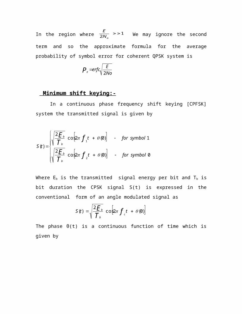
The vectors x and w are sampled values of the random vectors X and W respectively. the noise vector w represents that portion of the noise w(t) which will interfere with the detected process.Based on the observation vector x, we represent the received signal s(t)by a point in the same Euclidean space, we refer this point as received signal point. The relation between them is as shown in the fig
Fig: Illustrating the effect of noise perturbation on location of the received signal point
In the detection problem , the observation vector x is given, we have to perform a mapping from x to an estimate of the transmitted symbol, in away that would minimize the average probability of symbol error in the decision. The maximum likelihood detector provides solution to this problem.
Optimum transmitter & receiver
Probability of error depends on signal to noise ratio As the SNR increases the probability of error decreases An optimum transmitter and receiver is one which maximize the SNR and
minimize the probability of error.

Correlative receiver
For an AWGN channel and for the case when the transmitted signals are equally likely, the optimum receiver consists of two subsystems1) .Receiver consists of a bank of M product-integrator or correlatorsΦ1(t) ,Φ2(t) …….ΦM(t) orthonormal functionThe bank of correlator operate on the received signal x(t) to produce observation vector x
ObservationVector x

2). Implemented in the form of maximum likelihood detector that operates on observation vector x to produce an estimate of the transmitted symbol mi i = 1 to M, in a way that would minimize the average probability of symbol error.The N elements of the observation vector x are first multiplied by the corresponding N elements of each of the M signal vectors s1, s2… sM , and the resulting products are successively summed in accumulator to form the corresponding set of Inner products {(x, sk)} k= 1, 2 ..M. The inner products are corrected for the fact that the transmitted signal energies may be unequal. Finally,the largest in the resulting set of numbers is selected and a corresponding decision on the transmitted message made.The optimum receiver is commonly referred as a correlation receiver
MATCHED FILTERScience each of t he orthonormal basic functions are Φ1(t) ,Φ2(t) …….ΦM(t) is assumed to be zero outside the interval Tt 0 . we can design a linear filter with impulse response hj(t), with the received signal x(t) the fitter output is given by the convolution integral
Suppose the impulse response of the system is
Then the filter output is
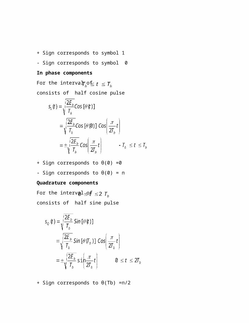
sampling this output at time t = T, we get
Φj(t) is zero outside the interval Tt 0 ,we get
yj(t) = xj
where xj is the j th correlator output produced by the received signal x(t).
A filter whose impulse response is time-reversed and delayed version of the input signal)(tj is said to be matched to )(tj . correspondingly , the optimum receiver based on
this is referred as the matched filter receiver.
For a matched filter operating in real time to be physically realizable, it must be causal.For causal system
causality condition is satisfied provided that the signal )(tj is zero outside the interval Tt 0
Maximization of output SNR in matched filter

Let x(t) = input signal to the matched filterh(t) = impulse response of the matched filterw(t) =white noise with power spectral density No/2
)(t = known signalInput to the matched filter is given by
science the filter is linear , the resulting output y(t) is given by
where )(0 t and n(t) are produced by the signal and noise components of the input x(t).
The signal to noise ratio at the output of the matched filter at t = T is
aim is to find the condition which maximize the SNR let
)()(
)()( 00
fHth
ft
are the Fourier transform pairs, hence the output signal )(0 t is given by
output at t = T is

For the receiver input noise with psd No/2 the receiver output noise psd is given by
and the noise power is given by
substituting the values of eqns 6.14 & 6.15 in 6.13 we get
using Schwarz’s inequality
Eqn 6.16 is equal when X1(f) = kX2*(f)
let X1(f) = H(f)& X2(f) = )2exp()( fTjf under equality condition
H(f) = K )19.6()2exp()(* fTjf
Thus substituting in 6.16 we get the value
dffdffHdffTjffH22
2
)()()2exp()()(
substituting in eqn 6,17 and simplifying
Using Rayleigh’s energy theorem

Under maximum SNR condition, the transfer function is given by ( k=1), eqn 6.19
The impulse response in time domain is given by
Thus the impulse response is folded and shifted version of the input signal )(t
MATCHED FILTER
Φ(t) = input signalh(t) = impulse responseW(t) =white noise
The impulse response of the matched filter is time-reversed and delayed version of the input signal

For causal system
Matched filter properties
PROPERTY 1The spectrum of the output signal of a matched filter with the matched signal as input is, except for a time delay factor, proportional to the energy spectral density of the input signal.let )(0 f denotes the Fourier transform of the filter output )(0 t , hence
PROPERTY 2
The output signal of a Matched Filter is proportional to a shifted version of the autocorrelation function of the input signal to which the filter is matched.The autocorrelation function and energy spectral density of a signal forms the Fourier transform pair, thus taking inverse Fourier transform for eqn 6.21
At time t = T
where E is energy of the signal
PROPERTY 3
The output Signal to Noise Ratio of a Matched filter depends only on the ratio of the signal energy to the power spectral density of the white noise at the filter input.
SNR at the output of matched filter is eqn 6.13
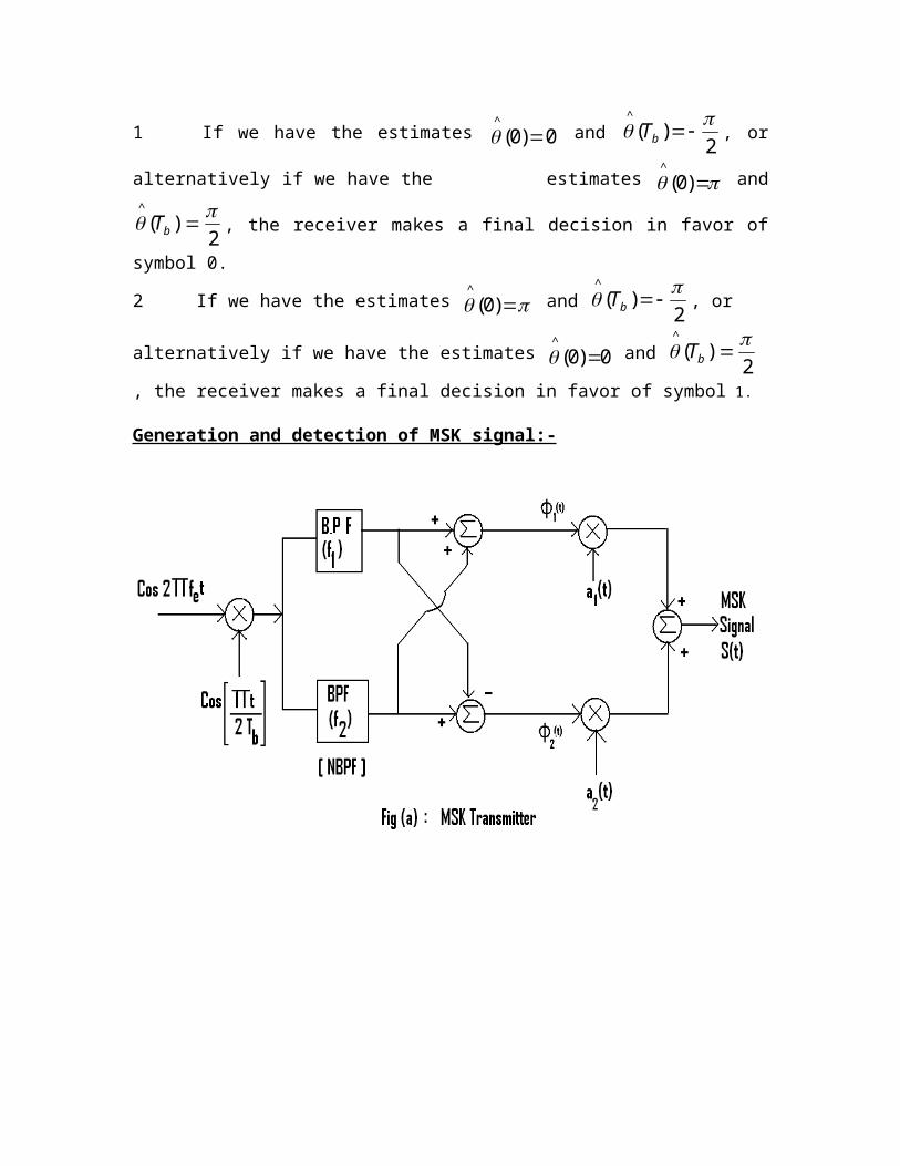
output of matched filter is
signal power at t = T
noise psd at the output of receiver is
noise power is
substituting the values in 6.22 we get
using Schwarz’s inequality
Eqn 6.24 is equal when X1(f) = kX2*(f)
let X1(f) = H(f)& X2(f) = )2exp()( fTjf under equality condition
H(f) = K )25.6()2exp()(* fTjf
Thus substituting in 6.24 we get the value
dffdffHdffTjffH22
2
)()()2exp()()(

substituting in eqn 6,23 and simplifying
Using Rayleigh’s energy theorem
PROPERTY 4
The Matched Filtering operation may be separated into two matching conditions; namely spectral phase matching that produces the desired output peak at time T, and the spectral amplitude matching that gives this peak value its optimum signal to noise density ratio.
In polar form the spectrum of the signal )(t being matched may be expressed as
where )( f is magnitude spectrum and )( f is phase spectrum of the signal.
The filter is said to be spectral phase matched to the signal )(t if the transfer function of the filter is defined by
The output of such a filter is
The product )()( ffH is real and non negative.

The spectral phase matching ensures that all the spectral components of the output add constructively at t = T , there by causing the output to attain its maximum value.
For spectral amplitude matching
Problem-1:
Consider the four signals s1(t), s2(t), s3(t) and s4(t) as shown in the fig-P1.1 . Use Gram-Schmidt Orthogonalization Procedure to find the orthonormal
basis for this set of signals. Also express the signals in terms of the basis functions.
Fig-P1.1: Signals for the problem -1.
Solution:
Given set is not linearly independent because s4(t) = s1(t) + s3(t)

Step-1: Energy of the signal s1(t)
3)(
0
211
TdttsE
T
First basis function 303)()(
1
11
TtforTE
tst
Step-2: Coefficient s21
T Tdtttss0 1221 3)()(
Energy of s2(t) 3
2)(
0
222
TdttsE
T
Second Basis function 32
33)()(
)(2212
12122
TtTforTsE
tstst
Step-3: Coefficient s31: T
dtttss0 1331 0)()(
Coefficient s32 T Tdtttss0 2332 3)()(
Intermediate functiong3(t) = s3(t) - s31Φ1(t) - s32 Φ2(t)
g3(t) = 1 for 2T/3 < t < T/3
Third Basis function
TtTforTdttg
tgt
T
3
23
)(
)()(
0
23
33
The corresponding orthonormal functions are shown in the figure-P1.2.
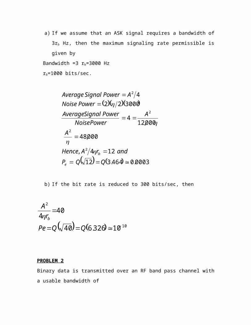
Fig-P1.2: Orthonormal functions for the Problem-1
Representation of the signals
)(3)( 11 tTtS
)(3)(3)( 212 tTtTtS
)(3)(3)( 323 tTtTtS
)(3)(3)(3)( 3214 tTtTtTtS

PROBLEM-2:
Consider the THREE signals s1(t), s2(t) and s3(t) as shown in the fig P2.1. Use Gram-Schmidt Orthogonalization Procedure to find the orthonormal basis for this set of signals. Also express the signals in terms of the basis functions.
Fig-P2.1: Signals for the problem -2.
Solution: The basis functions are shown in fig-P2.2.
Fig-P2.2: Orthonormal functions for the Problem-2
Correspondingly the representation of the signals are:
)(2)( 11 ttS
)(4)(4)( 212 tttS
)(3)(3)(3)( 3213 ttttS

PROBLEM-3:
Consider the signal s(t) in fig-P3.1a) Determine the impulse
response of a filter matched to this signal and sketch it as a function of time.
b) Plot the matched filter output as a function of time.
c) What is Peak value of the output?
Fig P3.1Solution:
The impulse response of the matched filter is time-reversed and delayed version of the input signal, h(t) = s(T-t) and the output of the filter, y(t) = x(t) * h(t).
Given s(t) = +1 for 0 < t < 0.5 -1 for 0.5 < t < 1.(a) With T = 1, the impulse
response h(t) is
h(t) = -1 for 0 < t < 0.5 +1 for 0.5 < t < 1.

Fig. P3.2
(b) The output of the filter y(t) is obtained by convolving the input s(t) and the impulse response h(t). The corresponding output is shown in the fig. P3.3.
(c) The peak value of the output is 1.0 unit.
Fig. P3.3
Assignment Problem:
Specify a matched filter for the signal S1(t) shown in Fig.-P4.1 Sketch the output of the filter matched to the signal S1(t) is applied to the filter input.
Fig P4.1
126

e-Notes by M.N.Suma, BMS, Bangalore
CHAPTER-4Line Codes
In base band transmission best way is to map digits or symbols into pulse
waveform. This waveform is generally termed as Line codes.
RZ: Return to Zero [ pulse for half the duration of Tb ]NRZ Return to Zero[ pulse for full duration of Tb ]
Unipolar (NRZ)
NRZ-inverted(differentialencoding)
1 0 1 0 1 1 0 01
UnipolarNRZ
Bipolarencoding
Manchesterencoding
DifferentialManchester
encoding
Polar NRZ
127
Unipolar NRZ

Unipolar NRZ“1” maps to +A pulse “0” maps to no pulse
Poor timing Low-frequency content Simple Long strings of 1s and 0s ,synchronization problem
Polar - (NRZ)
Polar NRZ“1” maps to +A pulse “0” to –A pulse
Better Average Power simple to implement Long strings of 1s and 0s ,synchronization problem Poor timing
Bipolar Code
• Three signal levels: {-A, 0, +A}• “1” maps to +A or –A in alternation• “0” maps to no pulse• Long string of 0’s causes receiver to loose synchronization • Suitable for telephone systems.
0
V
NRZ-Bipolar
1 111 10 0 00
128

Manchester code
• “1” maps into A/2 first for Tb/2, and -A/2 for next Tb/2• “0” maps into -A/2 first for Tb/2, and A/2 for Tb/2• Every interval has transition in middle
– Timing recovery easy• Simple to implement• Suitable for satellite telemetry and optical communications
Differential encoding It starts with one initial bit .Assume 0 or 1. Signal transitions are used for encoding.
Example NRZ - S and NRZ – M NRZ –S : symbol 1 by no transition , Symbol 0 by transition. NRZ-M : symbol 0 by no transition , Symbol 1 by transition Suitable for Magnetic recording systems.
M-ary formats Bandwidth can be properly utilized by employing M-ary formats. Here
grouping of bits is done to form symbols and each symbol is assigned some level. Example
Polar quaternary format employs four distinct symbols formed by dibits. Gray and natural codes are employed
Parameters in choosing formats
1. Ruggedness
2. DC Component
3. Self Synchronization.
4. Error detection
5. Bandwidth utilization
6. Matched Power Spectrum
1 0 1 0 1 1 0 01
Manchester Encoding
129

Power Spectra of Discrete PAM Signals:The discrete PAM signals can be represented by random process
Where Ak is discrete random variable, V(t) is basic pulse, T is symbol
duration. V(t) normalized so that V(0) = 1.
Coefficient Ak represents amplitude value and takes values for different
line codes as
Unipolar
Polar
Bipolar Manchester
As Ak is discrete random variable, generated by random process X(t),
We can characterize random variable by its ensemble averaged auto correlation
function given by
RA(n) = E [Ak.Ak-n] ,
Ak, Ak-n = amplitudes of kth and (k-n)th symbol position
PSD & auto correlation function form Fourier Transform pair & hence auto
correlation function tells us something about bandwidth requirement in frequency
domain.
Hence PSD Sx(f) of discrete PAM signal X(t).is given by
130

Where V(f) is Fourier Transform of basic pulse V(t). V(f) & RA(n) depends on
different line codes.
Power Spectra of NRZ Unipolar Format
Consider unipolar form with symbol 1’s and 0’s with equal probability i.e.P(Ak=0) = ½ and P(Ak=1) = ½
For n=0; Probable values of Ak.Ak = 0 x 0 & a x a
=E [ Ak.Ak-0] = E[Ak
2] = 02 x P [ Ak=0] + a2 x P[Ak=1]RA(0) = a2/2
If n ≠ 0Ak.Ak-n will have four possibilities (adjacent bits) 0 x 0, 0 x a, a x 0, a x a with probabilities ¼ each. E[Ak.Ak-n] = 0 x ¼ + 0 x ¼ + 0 x ¼ + a2 / 4
= a2 / 4 V(t) is rectangular pulse of unit amplitude, its Fourier Transform will be sinc function. V(f) = FT [ V(t)] = Tb Sinc (fTb) PSD is given by
substituting the values of V(f) and RA(n)
131

using Poisson’s formula
n
)b
Tnδ(f is Dirac delta train which multiplies Sinc function which
has nulls at
As a result,
Where δ(f) is delta function at f = 0, Therefore
Power Spectra of Bipolar Format
Here symbol 1 has levels ± a, and symbol 0 as 0. Totally three levels.Let 1’s and 0’s occur with equal probability then
P(AK = a) = 1/4 For Symbol 1 P(AK = -a) = 1/4 P(AK = 0) = 1/2 For Symbol 0
For n=0
132

E[AK2] = a x a P(AK = a) + (0 x 0) P[AK = 0] +
(-a x –a) P(AK = -a) = a2/4 + 0 + a2/4 = a2/2
For n≠0, i.e. say n=1; Four possible forms of AK.AK-1
00,01,10,11 i.e. dibits are 0 X 0, 0 X ±a, ±a X 0, ±a X ±a with equal probabilities ¼.
E[AK.AK-1] = 0 x ¼ + 0 x ¼ + 0 x ¼ - a2 x ¼ = -a2/4
For n>1, 3 bits representation 000,001,010 . . . . . . 111. i.e. with each probability of 1/8 which results in
E[AK.AK-n] = 0
a2 / 2 n = 0Therefore RA(n) = -a2 / 4 n = ±1 0 n > 1
PSD is given by
133
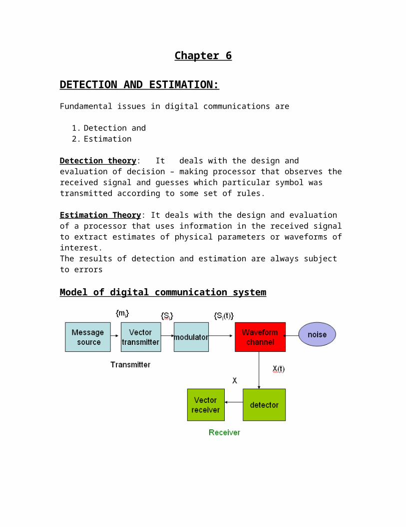
Spectrum of Line codes
• Unipolar most of signal power is centered around origin and there is
waste of power due to DC component that is present.
• Polar format most of signal power is centered around origin and they are
simple to implement.
• Bipolar format does not have DC component and does not demand more
bandwidth, but power requirement is double than other formats.
• Manchester format does not have DC component but provides proper
clocking.
Spectrum suited to the channel. • The PSD of the transmitted signal should be compatible with the
channel frequency response
• Many channels cannot pass dc (zero frequency) owing to ac
coupling
• Low pass response limits the ability to carry high frequencies
Inter symbol Interference
Generally, digital data is represented by electrical pulse, communication channel
is always band limited. Such a channel disperses or spreads a pulse carrying
digitized samples passing through it. When the channel bandwidth is greater
134

than bandwidth of pulse, spreading of pulse is very less. But when channel
bandwidth is close to signal bandwidth, i.e. if we transmit digital data which
demands more bandwidth which exceeds channel bandwidth, spreading will
occur and cause signal pulses to overlap. This overlapping is called Inter
Symbol Interference. In short it is called ISI. Similar to interference caused by
other sources, ISI causes degradations of signal if left uncontrolled. This
problem of ISI exists strongly in Telephone channels like coaxial cables and
optical fibers.
In this chapter main objective is to study the effect of ISI, when digital data
is transmitted through band limited channel and solution to overcome the
degradation of waveform by properly shaping pulse.
1 0 1 1
Tb
Transmitted Waveform Pulse Dispersion
The effect of sequence of pulses transmitted through channel is shown in
fig. The
Spreading of pulse is greater than symbol duration, as a result adjacent pulses
interfere. i.e. pulses get completely smeared, tail of smeared pulse enter into
adjacent symbol intervals making it difficult to decide actual transmitted pulse.
First let us have look at different formats of transmitting digital data.In
base band transmission best way is to map digits or symbols into pulse
waveform. This waveform is generally termed as Line codes .
BASEBAND TRANSMISSION:
135
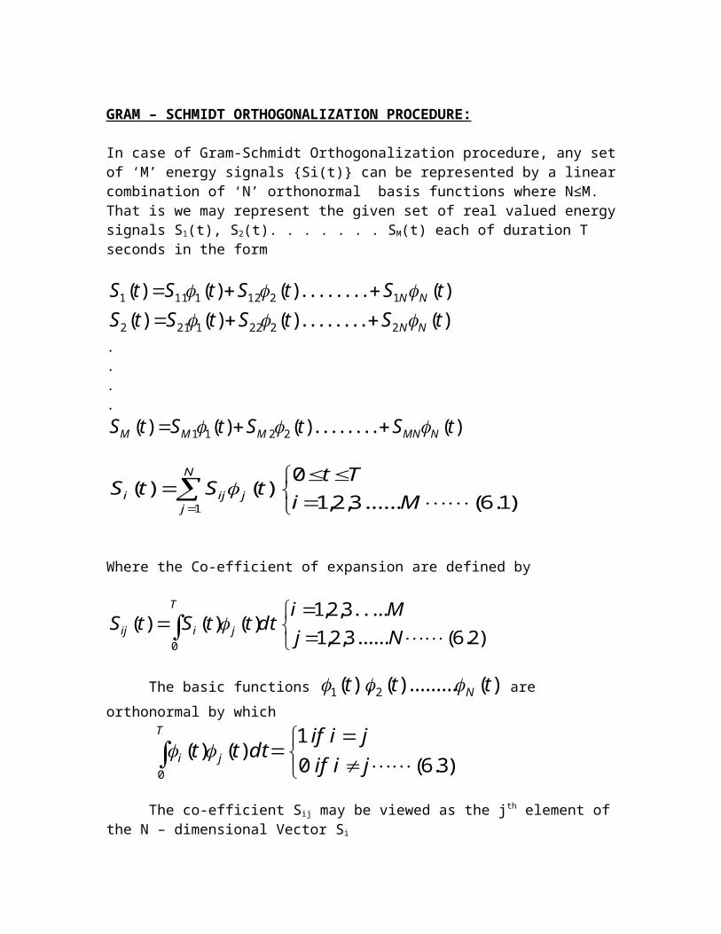
PAM signal transmitted is given by -------------------------- (1)
V(t) is basic pulse, normalized so that V(0) = 1,
x(t) represents realization of random process X(t) and ak is sample value of
random variable ak which depends on type of line codes.
The receiving filter output
---------------(2)
The output pulse μ P(t) is obtained because input signal ak .V(t) is passed through series of systems with transfer functions HT(f), HC(f), HR(f)
Therefore μ P(f) = V(f). HT(f).HC(f).HR(f) --------- (3)
P(f) p(t) and V(f) v(t)
The receiving filter output y(t) is sampled at ti = iTb. where ‘i’ takes intervals i = ±1, ±2 . . . . .
K
bbkb KTiTPaiTy )()(
K
bbkib KTiTPaPaiTy )()0()( ---------------------(4)
136

K = i K≠i
In equation(4) first term μai represents the output due to ith transmitted bit.
Second term represents residual effect of all other transmitted bits that are
obtained while decoding ith bit. This unwanted residual effect indicates ISI. This
is due to the fact that when pulse of short duration Tb is transmitted on band
limited channel, frequency components of the pulse are differentially attenuated
due to frequency response of channel causing dispersion of pulse over the
interval greater than Tb.
In absence of ISI desired output would have y (ti) = μai
Nyquist Pulse Shaping Criterion
In detection process received pulse stream is detected by sampling at
intervals ±KTb, then in detection process we will get desired output. This
demands sample of ith transmitted pulse in pulse stream at Kth sampling interval
should be
P(iTb – KTb) = 1 K=i
0 K≠i ------------- (5)
If received pulse P(t) satisfy this condition in time domain, then
y(ti) = μai
Let us look at this condition by transform eqn(5) into frequency domain.
Consider sequence of samples {P(nTb)} where n=0,±1. . . . . . . by sampling in time domain, we write in frequency domain
n
bb
TnfpT
fp )/(1
)( ----------------(6)
Where pδ(f) is Fourier transform of an infinite period sequence of delta functions of period Tb but pδ(f) can be obtained from its weighted sampled P(nTb) in time domain
)().()()()( 2 ttpdtemTtmTpfpm
ftjbb
137

Where m = i-k, then i=k, m=0; so
dtetpfp ftj 2)()0()(
Using property of delta function
i.e 1)(
dtt
Therefore 1)0()( pfp
Pδ(f) = 1 ------------(7)p(0) =1 ,i.e pulse is normalized (total area in frequency domain is unity)
Comparing (7) and (6)
1)/(1
nb
b
TnfpT
Or b
bn
b RTTnfp
1)/(
----------- (8)
Where Rb = Bit RateIs desired condition for zero ISI and it is termed Nyquist’s first criterion for
distortion less base band transmission. It suggests the method for constructing band limited function to overcome effect of ISI.
Ideal SolutionIdeal Nyquist filter that achieves best spectral efficiency and avoids ISI is
designed to have bandwidth as suggested
B0 = 1/2Tb (Nyquist bandwidth) = Rb/2
ISI is minimized by controlling P(t) in time domain or P(f) to be rectangular function in frequency domain.
138

Impulse response in time domain is given by
Disadvantage of Ideal solution • P(f) to be flat from –Bo to +Bo and zero else where , abrupt transition is
physically not realizable. • For large values of ‘ t’ , function P(t) decreases as resulting in slower
decay of sinc function due to discontinuity of P(f) This causes timing error which results in ISI.
Practical solution Raised Cosine Spectrum
• To design raised cosine filter which has transfer function consists of a flat portion and a roll off portion which is of sinusoidal form
• Bandwidth is an adjustable value between Bo and 2Bo.
P(f) =
139

The frequency f1 and bandwidth Bo are related by
α is called the roll off factor
for α = 0, f1=Bo and BW=Bo is the minimum Nyquist bandwidth for the .
rectangular spectrum.
• For given Bo , roll off factor ‘α’ specifies the required excess bandwidth
• α =1,indicates required excess bandwidth is 100% as roll off
characteristics of P(f) cuts off gradually as compared with ideal low pass
filters. This function is practically realizable.
Impulse response P(t) is given by
140

P(t) has two factors
• sinc(2Bot) which represents ideal filter - ensures zero crossings
• second factor that decreases as - helps in reducing tail of sinc pulse i.e. fast decay
• For α =1,
At p(t)=0.5
Pulse width measured exactly equal to bit duration Tb. Zero crossings occur at
t = ±3Tb, ±5Tb… In addition to usual crossings at t = ±Tb, ±2Tb… Which helps in
time synchronization at receiver at the expense of double the transmission
bandwidth
Transmission bandwidth required can be obtained from the relation B = 2Bo- f1
Where B = Transmission bandwidth Bo = Nyquist bandwidth
But using f1 = B0 (1- α) B = 2 B0 – B0(1- α) therefore B = B0(1+ α)
α =0; B=B0, minimum band width
α =1; B=2B0 , sufficient bandwidth
141

Roll-off factor
Smaller roll-off factor:
• Less bandwidth, but
• Larger tails are more sensitive to timing errors
Larger roll-off factor:
• Small tails are less sensitive to timing errors, but
• Larger bandwidth
Example1
A certain telephone line bandwidth is 3.5Khz .calculate data rate in bps that can be transmitted if binary signaling with raised cosine pulses and roll off factor α = 0.25 is employed.
Solution:α = 0.25 ---- roll off B = 3.5Khz ---transmission bandwidth
B = Bo(1+ α)
B0 = Ans: Rb= 5600bps
Example2
A source outputs data at the rate of 50,000 bits/sec. The transmitter uses binary PAM with raised cosine pulse in shaping of optimum pulse width. Determine the bandwidth of the transmitted waveform. Given a.α = 0 b.α = 0.25 c. α = 0.5 d. α = 0.75 e. α = 1
Solution B = B0(1+ α) B0=Rb/2a. Bandwidth = 25,000(1 + 0) = 25 kHzb. Bandwidth = 25,000(1 + 0.25) = 31.25 kHzc. Bandwidth = 25,000(1 + 0.5) = 37.5 kHzd. Bandwidth = 25,000(1 + 0.75) = 43.75 kHze. Bandwidth = 25,000(1 + 1) = 50 kHz
Example 3
142
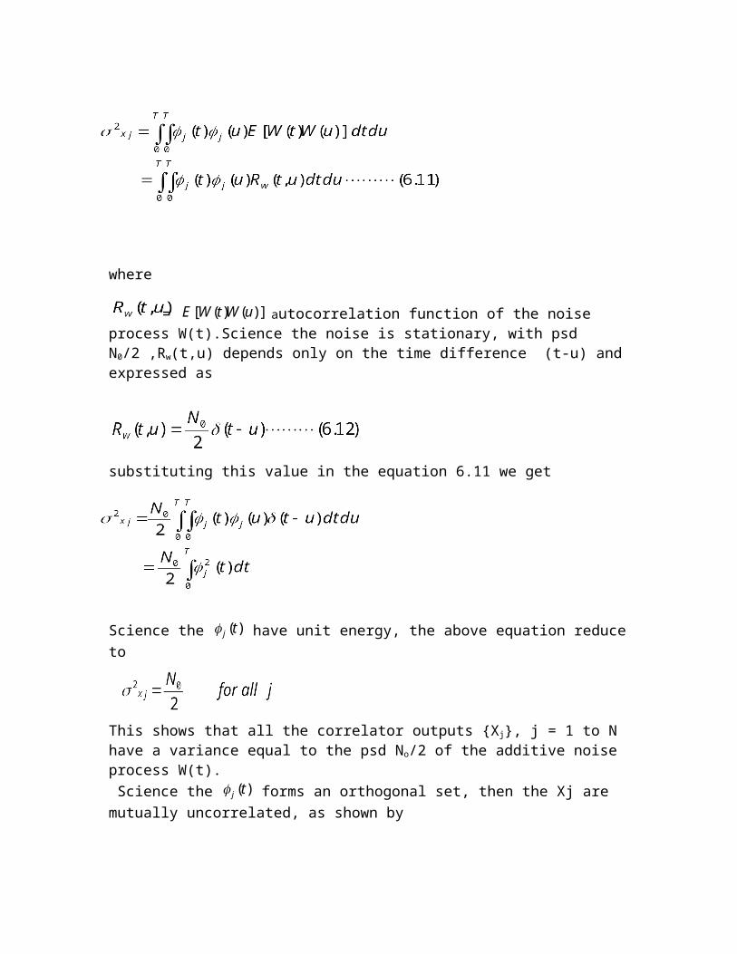
A communication channel of bandwidth 75 KHz is required to transmit binary data at a rate of 0.1Mb/s using raised cosine pulses. Determine the roll off factor α.Rb = 0.1MbpsB=75Khz α = ? B = Bo(1+ α) B0 = Rb/2 Ans : α =0.5
Correlative coding :
So far we treated ISI as an undesirable phenomenon that produces a
degradation in system performance, but by adding ISI to the transmitted signal in
a controlled manner, it is possible to achieve a bit rate of 2Bo bits per second in a
channel of bandwidth Bo Hz. Such a scheme is correlative coding or partial-
response signaling scheme. One such example is Duo binary signaling.
Duo means transmission capacity of system is doubled.
Duo binary coding
143
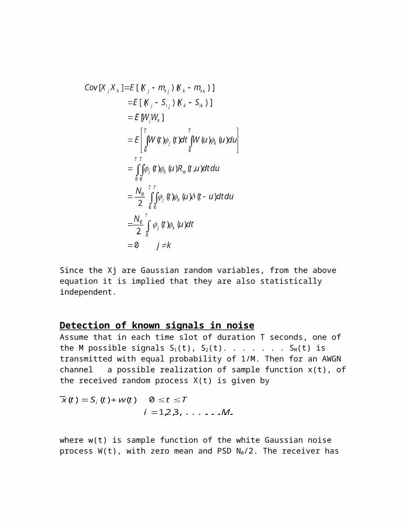
Consider binary sequence {bk} with uncorrelated samples transmitted at the rate
of Rb bps. Polar format with bit duration Tb sec is applied to duo binary
conversion filter. when this sequence is applied to a duobinary encoder, it is
converted into three level output, namely -2, 0 and +2.To produce this
transformation we use the scheme as shown in fig.The binary sequence {bk} is
first passed through a simple filter involving a single delay elements. For every
unit impulse applied to the input of this filter, we get two unit impulses spaced Tb
seconds apart at the filter output. Digit Ck at the output of the duobinary encoder
is the sum of the present binary digit bk and its previous value bk-1
Ck = bk + bk-1
The correlation between the pulse amplitude Ck comes from bk and previous bk-1
digit, can be thought of as introducing ISI in controlled manner., i.e., the
interference in determining {bk} comes only from the preceding symbol {bk-1} The
symbol {bk} takes ±1 level thus Ck takes one of three possible values -2,0,+2 .
The duo binary code results in a three level output. in general, for M-ary
transmission, we get 2M-1 levels
Transfer function of Duo-binary Filter
The ideal delay element used produce delay of Tb seconds for impulse will have
transfer function e -j 2π f Tb .
Overall transfer function of the filter H(f)
144

As ideal channel transfer function
Thus overall transfer function
H(f) which has a gradual roll off to the band edge, can also be implemented by
practical and realizable analog filtering Fig shows Magnitude and phase plot of
Transfer function
145

Advantage of obtaining this transfer function H(f) is that practical implementation
is easy
Impulse response
Impulse response h(t) is obtained by taking inverse Fourier transformation of
H(f)
146

1Tπt
Tb
πt
b
sin2bT
)(
th
Impulse response has two sinc pulses displaced by Tb sec. Hence overall impulse response has two distinguishable values at sampling instants t = 0 and t = Tb.
Overall Impulse response
147

Duo binary decoding
Encoding : During encoding the encoded bits are given by
Ck = bk + bk-1
Decoding:
At the receiver original sequence {bk} may be detected by subtracting the
previous decoded binary digit from the presently received digit Ck This
demodulation technique (known as nonlinear decision feedback equalization) is
essentially an inverse of the operation of the digital filter at the transmitter
if is estimate of original sequence bk then
Disadvantage
If Ck and previous estimate is received properly without error then we
get correct decision and current estimate Otherwise once error made it tends to
propagate because of decision feed back. current {bk} depends on previous bk-1.
148

Example consider sequence 0010110
PrecodingIn case of duo binary coding if error occurs in a single bit it reflects as multiple
errors because the present decision depends on previous decision also. To
make each decision independent we use a precoder at the receiver before
performing duo binary operation.
The precoding operation performed on the input binary sequence {bk}
converts it into another binary sequence {ak} given by
a modulo 2 logical addition
Unlike the linear operation of duo binary operation, the precoding is a non
linear operation.
149

Fig. A precoded duo binary scheme.
{ak} is then applied to duobinary coder, which produce sequence {Ck}
If that symbol at precoder is in polar format Ck takes three levels,
The decision rule for detecting the original input binary sequence {bk} from {ck} is
150

Example: with start bit as 0, reference bit 1
Example: with start bit as 0, reference bit 0
151

Example: with start bit as 1, reference bit 1
Example: with start bit as 1, reference bit 0
152

Today the duo-binary techniques are widely applied throughout the world.
While all current applications in digital communications such as data
transmission, digital radio, and PCM cable transmission, and other new
possibilities are being explored.
This technique has been applied to fiber optics and to high density disk recording
which have given excellent results
Example
The binary data 001101001 are applied to the input of a duo binary system.
a)Construct the duo binary coder output and corresponding receiver output,
without a precoder.
b) Suppose that due to error during transmission, the level at the receiver input
produced by the second digit is reduced to zero. Construct the new receiver
output.
c) Repeat above two cases with use of precoder
without a precoder
errors errors
153
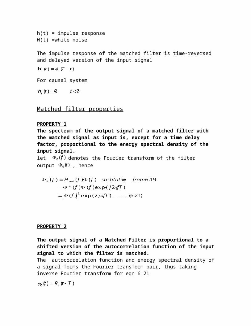
With a precoder (start bit 1)
With a precoder (start bit 0)
154

The Transfer function H(f) of Duo binary signalling has non zero spectral value at origin, hence not suitable for channel with Poor DC response. This drawback is corrected by Modified Duobinary scheme.
Modified Duobinary scheme.
It is an extension of the duo-binary signaling. The modified duo binary technique involves a correlation span of two binary digits. Two-bit delay causes the ISI to spread over two symbols. This is achieved by subtracting input binary digits spaced 2Tb secs apart.
Modified Duobinary scheme.
155
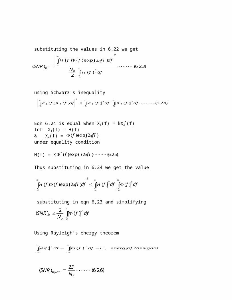
Transmitter
The precoded output sequence is given by a modulo 2 logical addition
If ak = ± 1v , Ck takes one of three values 2,0,-2.
Output sequence of modified duo binary filter is given by Ck
Ck = ak – ak-2
Ck takes one of three values 2,0,-2
Ck = 0V, if bk is represented by symbol 0Ck = +2V, if bk is represented by symbol 1
Receiver At the receiver we may extract the original sequence {bk} using the decision rule bk = symbol 0 if |Ck| >1v symbol 1 if |Ck| ≤1v
The Transfer function of the filter is given by
156

The Transfer function has zero value at origin, hence suitable for poor dc channels
Impulse response
Impulse response h(t) is obtained by taking Inverse Fourier transformation of H(f)
157

Impulse response has three distinguishable levels at the sampling instants.
158
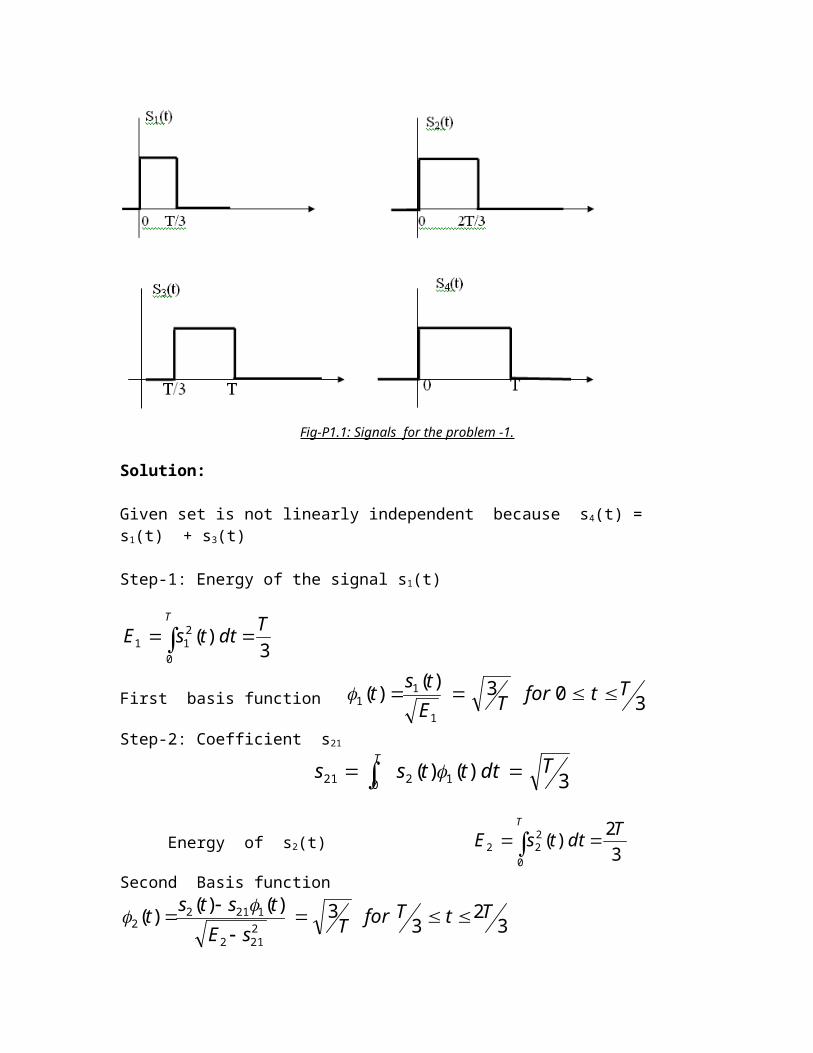
To eliminate error propagation modified duo binary employs Precoding option same as previous case.
Prior to duo binary encoder precoding is done using modulo-2 adder on signals spaced 2Tb apart
Example : Consider binary sequence {bk}= {01101101} applied to input of a precoded modified duobinary filter. Determine receiver output and compare with original {bk}.
159

Consider binary sequence {bk}={01101101}
Example
The binary data 011100101 are applied to the input of a modified duo binary
system.
a) Construct the modified duobinary coder output and corresponding receiver
output, without a precoder.
b) Suppose that due to error during transmission, the level at the receiver input
produced by the third digit is reduced to zero. Construct the new receiver output.
c) Repeat above two cases with use of precoder
Modified duobinary coder output and corresponding receiver output, without a precoder
160

Modified duo binary coder output and corresponding receiver output, with a precoder
161

Generalized form of correlative coding scheme
Fig. Generalized Correlative Coding
162
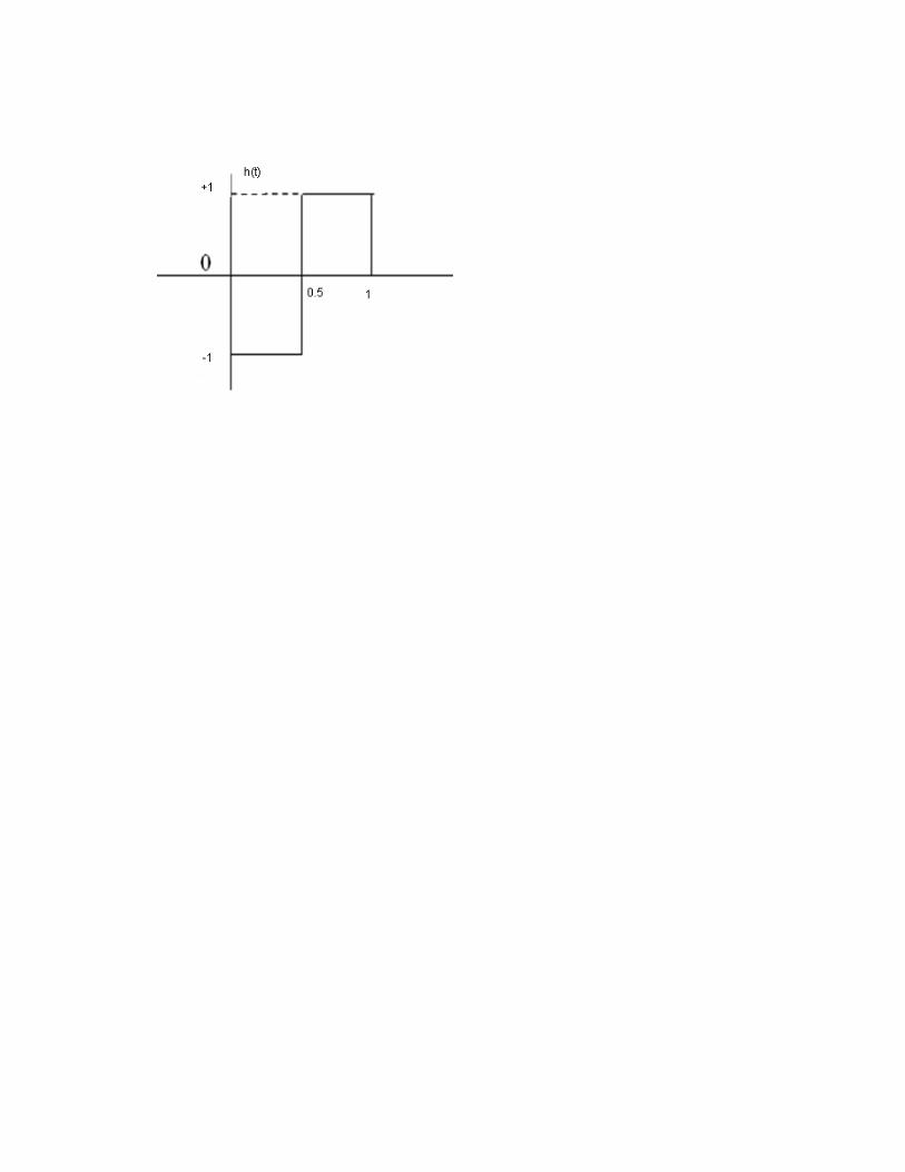
The Duo binary and modified Duo binary scheme have correlation spans of one binary digit and two binary digits respectively. This generalisation scheme involves the use of a tapped delay line filter with tap weights f0, f1, f2,… fn-1. A correlative samples Ck is obtained from a superposition of ‘N’ successive input sample values bK
Ck =
By choosing various combination values for fn, different correlative coding schemes can be obtained from simple duo binary.
Base band Transmission of M-ary data
In base band M-ary PAM, output of the pulse generator may take on any one of the M-possible amplitude levels with M>2 for each symbolThe blocks of n- message bits are represented by M-level waveforms with M=2n.
Ex: M=4 has 4 levels. possible combination are 00, 10, 11, 01
T= 2Tb is termed symbol duration .In general symbol duration T = Tb log 2M.
M-ary PAM system is able to transmit information at a rate of log2M faster than binary PAM for given channel bandwidth.
Mlog2
RbR
Rb = bit rate for binary systemR = symbol rate for binary system
M-ary PAM system requires more power which is increased by factor equal to
for same average probability of symbol error.
M-ary Modulation is well suited for the transmission of digital data over channels that offer a limited bandwidth and high SNR
Example
163

An analog signal is sampled, quantised and encoded into a binary PCM
wave. The number of representation levels used is 128. A synchronizing
pulse is added at the end of each code word representing a sample of the
analog signal. The resulting PCM wave is transmitted over a channel of
bandwidth 12kHz using binary PAM system with a raised cosine spectrum.
The roll off factor is unity.
a)Find the rate (in BPS ) at which information is transmitted through the
channel.
b) Find the rate at which the analog signal is sampled. What is the
maximum possible value for the highest frequency component of the
analog signal.
SolutionGiven Channel with transmission BW B=12kHz.Number of representation levels L = 128Roll off α = 1 a) B = Bo(1+ α), Hence Bo =6kHz.Bo=Rb/2 therefore Rb = 12kbps.
b) For L=128, L = 2n , n = 7 symbol duration T = Tb log2M =nTb sampling rate fs = Rb/n = 12/7 = 1.714kHz. And maximum frequency component of analog signal is From LP sampling theorem w = fs/2 = 857Hz.
Eye pattern
The quality of digital transmission systems are evaluated using the bit
error rate. Degradation of quality occurs in each process modulation,
transmission, and detection. The eye pattern is experimental method that
contains all the information concerning the degradation of quality. Therefore,
careful analysis of the eye pattern is important in analyzing the degradation
mechanism.
164
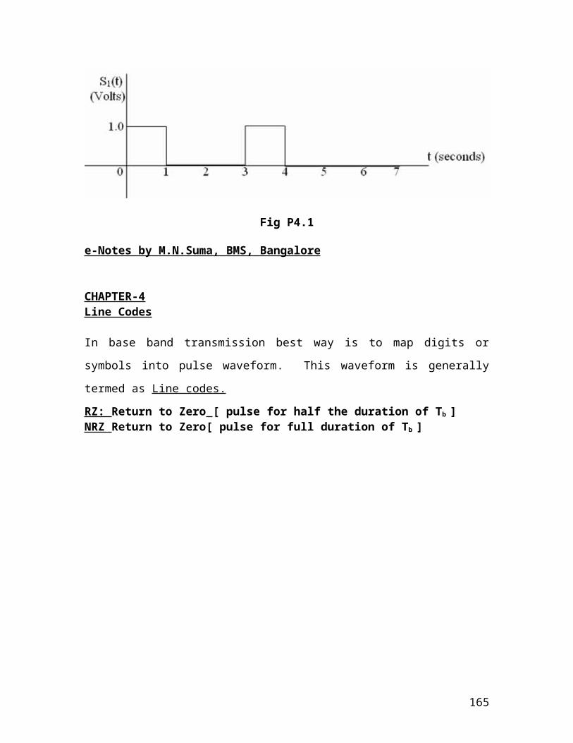
• Eye patterns can be observed using an oscilloscope. The received wave
is applied to the vertical deflection plates of an oscilloscope and the
sawtooth wave at a rate equal to transmitted symbol rate is applied to the
horizontal deflection plates, resulting display is eye pattern as it resembles
human eye.
• The interior region of eye pattern is called eye opening
We get superposition of successive symbol intervals to produce eye pattern as shown below.
• The width of the eye opening defines the time interval over which the received wave can be sampled without error from ISI
• The optimum sampling time corresponds to the maximum eye opening
• The height of the eye opening at a specified sampling time is a measure of the margin over channel noise.
165

The sensitivity of the system to timing error is determined by the rate of closure of the eye as the sampling time is varied.
Any non linear transmission distortion would reveal itself in an asymmetric or squinted eye. When the effected of ISI is excessive, traces from the upper portion of the eye pattern cross traces from lower portion with the result that the eye is completely closed.
Example of eye pattern:
Binary-PAM Perfect channel (no noise and no ISI)
Example of eye pattern: Binary-PAM with noise no ISI
Example 1
A binary wave using polar signaling is generated by representing symbol 1 by a pulse of amplitude -1v; in both cases the pulse duration equals the bit duration. The signal is applied to a low pass RC filter with transfer function
Construct eye pattern for the filter for1. Alternating 1s and 0s2. A long sequence of 1s followed by long sequence of zeros.
166

Example 2
The binary sequence 011010 is transmitted through channel having a raised cosine characteristics with roll off factor unity. Assume the use of polar signaling, format. construct the Eye pattern
167
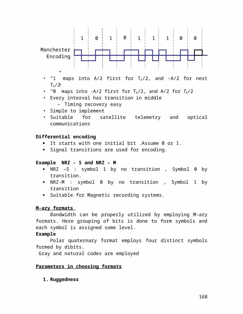
0 1 1 0 1 0Eye Pattern
Adaptive equalization for data transmission
This technique is another approach to minimize signal distortion in the
base band data transmission. This is Nyquist third method for controlling ISI.
Equalization is essential for high speed data transmission over voice
grade telephone channel which is essentially linear and band limited.
High speed data transmission involves two basic operations:
i) Discrete pulse amplitude modulation:
The amplitudes of successive pulses in a periodic pulse train are varied in
a discrete fashion in accordance with incoming data stream.
ii) Linear modulation:
Which offers band width conservation to transmit the encoded pulse train
over telephone channel.
At the receiving end of the systems, the received waves is demodulated
and then synchronously sampled and quantized. As a result of dispersion of the
pulse shape by the channel the number of detectable amplitude levels is limited
by ISI rather than by additive noise. If the channel is known , then it is possible to
make ISI arbitrarily small by designing suitable pair of transmitting and receiving
filters for pulse shaping.
In switched telephone networks we find that two factors contribute to pulse
distortion.
1. Differences in the transmission characteristics of individual links that may be
switched together.
168

2. Differences in number of links in a connection
Because of these two characteristics, telephone channel is random in nature.
To realize the full transmission capability of a telephone channel we need
adaptive equalization.
Adaptive equalization
• An equalizer is a filter that compensates for the dispersion effects of a channel. Adaptive equalizer can adjust its coefficients continuously during the transmission of data.
Pre channel equalization requires feed back channel causes burden on transmission.
Post channel equalization Achieved prior to data transmission by training the filter with the guidance
of a training sequence transmitted through the channel so as to adjust the filter parameters to optimum values.
Adaptive equalization – It consists of tapped delay line filter with set of delay elements, set of adjustable multipliers connected to the delay line taps and a summer for adding multiplier outputs.
169

The output of the Adaptive equalizer is given by
Ci is weight of the ith tap Total number of taps are M .Tap spacing is equal to symbol duration T of transmitted signalIn a conventional FIR filter the tap weights are constant and particular designed response is obtained. In the adaptive equaliser the Ci's are variable and are adjusted by an algorithm
Two modes of operation
1. Training mode 2 . Decision directed mode
Mechanism of adaptation
Training mode
A known sequence d(nT) is transmitted and synchronized version of it is generated in the receiver applied to adaptive equalizer.
This training sequence has maximal length PN Sequence, because it has large average power and large SNR, resulting response sequence (Impulse) is observed by measuring the filter outputs at the sampling instants.
The difference between resulting response y(nT) and desired response d(nT)is error signal which is used to estimate the direction in which the coefficients of filter are to be optimized using algorithms
170

Methods of implementing adaptive equalizer
i) Analog ii) Hard wired digitaliii) Programmable digital
Analog method
Charge coupled devices [CCD’s] are used. CCD- FET’s are connected in series with drains capacitively coupled to
gates.
The set of adjustable tap widths are stored in digital memory locations, and the multiplications of the analog sample values by the digitized tap weights done in analog manner.
Suitable where symbol rate is too high for digital implementation.
Hard wired digital technique
• Equalizer input is first sampled and then quantized in to form that is suitable for storage in shift registers.
• Set of adjustable lap weights are also stored in shift registers. Logic circuits are used for required digital arithmetic operations.
• widely used technique of equalization
Programmable method
• Digital processor is used which provide more flexibility in adaptation by programming.
• Advantage of this technique is same hardware may be timeshared to perform a multiplicity of signal processing functions such as filtering, modulation and demodulation in modem.
171

CHAPTER-7
Spread – Spectrum Modulation
Introduction:
Initially developed for military applications during II world war, that was less
sensitive to intentional interference or jamming by third parties.
Spread spectrum technology has blossomed into one of the fundamental building
blocks in current and next-generation wireless systems
Problem of radio transmission
Narrow band can be wiped out due to interference
To disrupt the communication, the adversary needs to do two things,
(a) to detect that a transmission is taking place and
(b) to transmit a jamming signal which is designed to confuse the receiver.
.Solution
A spread spectrum system is therefore designed to make these tasks as difficult
as possible.
Firstly, the transmitted signal should be difficult to detect by an
adversary/jammer, i.e., the signal should have a low probability of intercept (LPI).
Secondly, the signal should be difficult to disturb with a jamming signal, i.e., the
transmitted signal should possess an anti-jamming (AJ) property
Remedy
spread the narrow band signal into a broad band to protect against
interference
In a digital communication system the primary resources are Bandwidth
and Power. The study of digital communication system deals with efficient
utilization of these two resources, but there are situations where it is necessary to
sacrifice their efficient utilization in order to meet certain other design objectives.
For example to provide a form of secure communication (i.e. the
transmitted signal is not easily detected or recognized by unwanted listeners) the
bandwidth of the transmitted signal is increased in excess of the minimum
bandwidth necessary to transmit it. This requirement is catered by a technique
known as “Spread Spectrum Modulation”.
172

The primary advantage of a Spread – Spectrum communication system is
its ability to reject ‘Interference’ whether it be the unintentional or the intentional
interference.
The definition of Spread – Spectrum modulation may be stated in two
parts.
1. Spread Spectrum is a mean of transmission in which the data sequence
occupies a BW (Bandwidth) in excess of the minimum BW necessary to
transmit it.
2. The Spectrum Spreading is accomplished before transmission through
the use of a code that is independent of the data sequence. The Same
code is used in the receiver to despread the received signal so that the
original data sequence may be recovered.
s(t) wide band r(t) wide band b(t) +
Noise
b(t) . . . . . . . . . . Narrow
Wide
Band
Band
c(t) n(t) c(t)
Wide band (noise) Wide band
---- Transmitter---- ---- Channel------ --- Receiver--------
fig:1 spread spectrum technique.
b(t) = Data Sequence to be transmitted (Narrow Band)
c(t) = Wide Band code
s(t) = c(t) * b(t) – (wide Band)
173

Fig: Spectrum of signal before & after spreading
PSUEDO-NOISE SEQUENCE:
Generation of PN sequence:
Clock
Output
S0 S1 S2 S3 Sequence
Logic Circuit
Fig 2: Maximum-length sequence generator for n=3
A feedback shift register is said to be Linear when the feed back logic
consists of entirely mod-2-address ( Ex-or gates). In such a case, the zero state
is not permitted. The period of a PN sequence produced by a linear feedback
shift register with ‘n’ flip flops cannot exceed 2n-1. When the period is exactly 2n-
1, the PN sequence is called a ‘maximum length sequence’ or ‘m-sequence’.
Example1: Consider the linear feed back shift register as shown in fig
2 involve three flip-flops. The input so is equal to the mod-2 sum of S1 and S3. If
the initial state of the shift register is 100. Then the succession of states will be
as follows.
100,110,011,011,101,010,001,100 . . . . . .
174
Shift Register1
Shift Register2
Shift Register3

The output sequence (output S3) is therefore. 00111010 . . . . .
Which repeats itself with period 23–1 = 7 (n=3)
Maximal length codes are commonly used PN codes In binary shift register, the maximum length sequence is
N = 2m-1
chips, where m is the number of stages of flip-flops in the shift register.
At each clock pulse • Contents of register shifts one bit right.• Contents of required stages are modulo 2 added and fed back
to input.
Fig: Initial stages of Shift registers 1000
Let initial status of shift register be 1000
175
1 0 0 00 1 0 00 0 1 01 0 0 11 1 0 00 1 1 01 0 1 10 1 0 11 0 1 01 1 0 11 1 1 01 1 1 10 1 1 10 0 1 10 0 0 1 1 0 0 0
• We can see for shift Register of length m=4. .At each clock the change in state of flip-flop is shown.
• Feed back function is modulo two of X3
and X4.
• After 15 clock pulses the sequence repeats.Output sequence is0 0 0 1 0 0 1 1 0 1 0 1 1 1 1
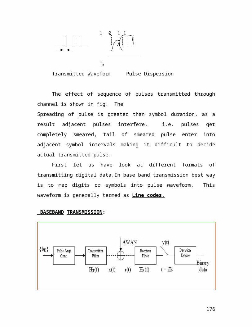
Properties of PN SequenceRandomness of PN sequence is tested by following properties
1. Balance property
2. Run length property
3. Autocorrelation property
1. Balance property
In each Period of the sequence , number of binary ones differ from binary zeros
by at most one digit .
Consider output of shift register 0 0 0 1 0 0 1 1 0 1 0 1 1 1 1Seven zeros and eight ones -meets balance condition.
2. Run length property
Among the runs of ones and zeros in each period, it is desirable that about one
half the runs of each type are of length 1, one- fourth are of length 2 and one-
eighth are of length 3 and so-on.
Consider output of shift register
Number of runs =8
3. Auto correlation propertyAuto correlation function of a maximal length sequence is periodic and binary
valued. Autocorrelation sequence of binary sequence in polar format is given by
176
0 0 0 1 0 0 1 1 0 1 0 1 1 1 1 3 1 2 2 1 1 1 4

Where N is length or period of the sequence and
k is the lag of the autocorrelation
Where l is any integer. we can also state Autocorrelation function as { No. of agreements – No. of disagreements in comparison of one full period } Consider output of shift register for l=1
Yields PN autocorrelation as
Range of PN Sequence Lengths
Length 0f Shift Register, m PN Sequence Length,
7 1278 2559 511
177

10 102311 204712 409513 819117 13107119 524287
A Notion of Spread Spectrum :
An important attribute of Spread Spectrum modulation is that it can
provide protection against externally generated interfacing signals with finite
power. Protection against jamming (interfacing) waveforms is provided by
purposely making the information – bearing signal occupy a BW far in excess of
the minimum BW necessary to transmit it. This has the effect of making the
transmitted signal a noise like appearance so as to blend into the background.
Therefore Spread Spectrum is a method of ‘camouflaging’ the information –
bearing signal.
V
b(t) m(t). . r(t) z(t)
c(t) n(t) c(t)
Threshold=0
<----Transmitter-----> --Channel - - - - - Receiver
-------------
Let { bK} denotes a binary data sequence.
{ cK } denotes a PN sequence.
b(t) and c(t) denotes their NRZ polar representation respectively.
The desired modulation is achieved by applying the data signal b(t) and PN
signal c(t) to a product modulator or multiplier. If the message signal b(t) is
narrowband and the PN sequence signal c(t) is wide band, the product signal
178
Decision Device
m(t) is also wide band. The PN sequence performs the role of a ‘Spreading
Code ”.
For base band transmission, the product signal m(t) represents the
transmitted signal. Therefore m(t) = c(t).b(t)
The received signal r(t) consists of the transmitted signal m(t) plus an
additive interference noise n(t), Hence
r(t) = m(t) + n(t)
= c(t).b(t) + n(t)
+1
0
-1
a) Data Signal b(t)
+1
0
-1
b)Spreading Code c(t)
+1
179

0
-1
c)Product signal or base band transmitted signal m(t)
To recover the original message signal b(t), the received signal r(t) is applied to a
demodulator that consists of a multiplier followed by an integrator and a decision
device. The multiplier is supplied with a locally generated PN sequence that is
exact replica of that used in the transmitter. The multiplier output is given by
Z(t) = r(t).c(t)
= [b(t) * c(t) + n(t)] c(t)
= c2(t).b(t) + c(t).n(t)
The data signal b(t) is multiplied twice by the PN signal c(t), where as unwanted
signal n(t) is multiplied only once. But c2(t) = 1, hence the above equation
reduces to
Z(t) = b(t) + c(t).n(t)
Now the data component b(t) is narrowband, where as the spurious component
c(t)n(t) is wide band. Hence by applying the multiplier output to a base band (low
pass) filter most of the power in the spurious component c(t)n(t) is filtered out.
Thus the effect of the interference n(t) is thus significantly reduced at the receiver
output.
The integration is carried out for the bit interval 0 ≤ t ≤ Tb to provide the sample
value V. Finally, a decision is made by the receiver.
If V > Threshold Value ‘0’, say binary symbol ‘1’
If V < Threshold Value ‘0’, say binary symbol ‘0’
Direct – Sequence Spread Spectrum with coherent binary Phase shift Keying:-
Binary data
b(t) m(t) x(t)
c(t)
Carrier
180
Binary PSK Modulator
PN Code Generator

a) Transmitter
Say 1 y(t) v v if v > 0Received Say 0Signal c(t) if v < 0
Local Carrier
b) Receiver
Fig: model of direct – sequence spread binary PSK system(alternative form)
To provide band pass transmission, the base band data sequence is
multiplied by a Carrier by means of shift keying. Normally binary phase shift
keying (PSK) is used because of its advantages.
The transmitter first converts the incoming binary data sequence {bk} into
an NRZ waveform b(t), which is followed by two stages of modulation.
181
Coherent Detector
Local PN generator
Decision Device
The first stage consists of a multiplier with data signal b(t) and the PN
signal c(t) as inputs. The output of multiplier is m(t) is a wideband signal. Thus a
narrow – band data sequence is transformed into a noise like wide band signal.
The second stage consists of a binary Phase Shift Keying (PSK)
modulator. Which converts base band signal m(t) into band pass signal x(t). The
transmitted signal x(t) is thus a direct – sequence spread binary PSK signal. The
phase modulation θ(t) of x(t) has one of the two values ‘0’ and ‘π’ (180o)
depending upon the polarity of the message signal b(t) and PN signal c(t) at time
t.
Polarity of PN & Polarity of PN signal both +, + or - - Phase ‘0’
Polarity of PN & Polarity of PN signal both +, - or - + Phase ‘π’
Polarity of data sequence b(t)
+ -
Polarity of PN sequence C(t) + 0 π
- π 0
The receiver consists of two stages of demodulation.
In the first stage the received signal y(t) and a locally generated carrier are
applied to a coherent detector (a product modulator followed by a low pass filter),
Which converts band pass signal into base band signal.
The second stage of demodulation performs Spectrum despreading by
multiplying the output of low-pass filter by a locally generated replica of the PN
signal c(t), followed by integration over a bit interval Tb and finally a decision
device is used to get binary sequence.
Signal Space Dimensionality and Processing Gain
Fundamental issue in SS systems is how much protection spreading
can provide against interference.
SS technique distribute low dimensional signal into large dimensional
signal space (hide the signal).
Jammer has only one option; to jam the entire space with fixed total
power or to jam portion of signal space with large power.
182
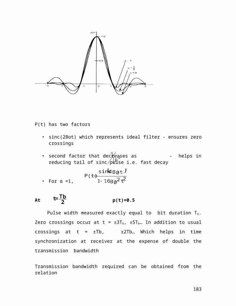
Consider set of orthonormal basis functions;
whereTc is chip duration,N is number of chips per bit.
Transmitted signal x(t) for the interval of an information bit is
where, Eb is signal energy per bit.PN Code sequence { c0, c1, ……cN-1} with ck= + 1 Transmitted signal x(t) is therefore N dimensional and requires N orthonormal functions to represent it.j(t) represent interfering signal (jammer). As said jammer tries to places all its available energy in exactly same N dimension signal space. But jammer has no knowledge of signal phase. Hence tries to place equal energy in two phase coordinates that is cosine and sine As per that jammer can be represented as
where
Thus j(t) is 2N dimensional, twice the dimension as that of x(t).
183
Average interference power of j(t)
as jammer places equal energy in two phase coordinates , hence
To evaluate system performance we calculate SNR at input and output of DS/BPSK receiver. The coherent receiver input is u(t) =s(t) + c(t)j(t)and using this u(t), output at coherent receiver
Where vs is despread component of BPSK and vcj of spread interference.
Consider despread BPSK signal s(t)
1N
0kbkjT
2J
2
1N
0k
21N
0k
2~
kjkj
184

Where + sign is for symbol 1 - sign for symbol 0.If carrier frequency is integer multiple of 1 / Tb , wehave
Consider spread interference component vcj
here c(t) is considered in sequence form { c0, c1, ……cN-1}
With Ck treated as independent identical random variables with both symbols having equal probabilities
Expected value of Random variable vcj is zero, for fixed k we have
and Variance
Spread factor N = Tb/Tc
Output signal to noise ratio is
The average signal power at receiver input is Eb/Tb hence input SNR
185

Expressing SNR in decibels
where
.3db term on right side accounts for gain in SNR due to coherent detection.
. Last term accounts for gain in SNR by use of spread spectrum. PG is called Processing Gain
1. Bit rate of binary data entering the transmitter input is
2. The bandwidth of PN sequence c(t) , of main lobe is Wc
186

Probability of error
To calculate probability of error, we consider output component v of coherent detector as sample value of random variable V
Eb is signal energy per bit and Vcj is noise component
Decision rule is, if detector output exceeds a threshold of zero volts; received bit is symbol 1 else decision is favored for zero.
• Average probability of error Pe is nothing but conditional probability which depends on random variable Vcj.
• As a result receiver makes decision in favor of symbol 1 when symbol 0 transmitted and vice versa
• Random variable Vcj is sum of N such random variables. Hence for Large N it can assume Gaussian distribution .
• As mean and variance has already been discussed , zero mean and variance JTc/2
Probability of error can be calculated from simple formula for DS/BPSK system
Antijam CharacteristicsConsider error probability of BPSK
Comparing both probabilities;
Since bit energy Eb =PTb , P= average signal power.
We can express bit energy to noise density ratio as
187

or
The ratio J/P is termed jamming margin. Jamming Margin is expressed in decibels as
Where is minimum bit energy to noise ratio needed to support a prescribed average probability of error.
Example1A pseudo random sequence is generated using a feed back shift register of length m=4. The chip rate is 107 chips per second. Find the following
a) PN sequence lengthb) Chip duration of PN sequencec) PN sequence period
Solutiona) Length of PN sequence N = 2m-1 = 24-1 =15b) Chip duration Tc = 1/chip rate =1/107 = 0.1µsecc) PN sequence period T = NTc
= 15 x 0.1µsec = 1.5µsec
Example2 A direct sequence spread binary phase shift keying system uses a feedback shift register of length 19 for the generation of PN sequence. Calculate the processing gain of the system.SolutionGiven length of shift register = m =19 Therefore length of PN sequence N = 2m - 1
= 219 - 1Processing gain PG = Tb/Tc =Nin db =10log10N = 10 log10 (219) = 57dbExample3
188

A Spread spectrum communication system has the following parameters. Information bit duration Tb = 1.024 msecs and PN chip duration of 1µsecs. The average probability of error of system is not to exceed 10-5. calculate a) Length of shift register b) Processing gain c) jamming marginSolutionProcessing gain PG =N= Tb/Tc =1024 corresponding length of shift register m = 10 In case of coherent BPSK For Probability of error 10-5.[Referring to error function table] Eb/N0 =10.8 Therefore jamming margin
= 30.10 – 10.33 = 19.8 dbFrequency – Hop Spread Spectrum:
In a frequency – hop Spread – Spectrum technique, the spectrum of data
modulated carrier is widened by changing the carrier frequency in a pseudo –
random manner. The type of spread – spectrum in which the carrier hops
randomly form one frequency to another is called Frequency – Hop (FH)
Spread Spectrum.
Since frequency hopping does not covers the entire spread spectrum
instantaneously. We are led to consider the rate at which the hop occurs.
Depending upon this we have two types of frequency hop.
1. Slow frequency hopping:- In which the symbol rate Rs of the MFSK signal
is an integer multiple of the hop rate Rh. That is several symbols are
transmitted on each frequency hop.
2. Fast – Frequency hopping:- In which the hop rate Rh is an integral multiple
of the MFSK symbol rate Rs. That is the carrier frequency will hoop
several times during the transmission of one symbol.
A common modulation format for frequency hopping system is that of
M- ary frequency – shift – keying (MFSK).
189
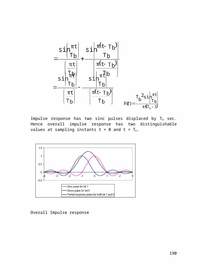
Slow frequency hopping:-
Fig.a) Shows the block diagram of an FH / MFSK transmitter, which involves
frequency modulation followed by mixing.
The incoming binary data are applied to an M-ary FSK modulator. The resulting modulated wave and the output from a digital frequency synthesizer are then applied to a mixer that consists of a multiplier followed by a band – pass filter. The filter is designed to select the sum frequency component resulting from the multiplication process as the transmitted signal. An ‘k’ bit segments of a PN sequence drive the frequency synthesizer, which enables the carrier frequency to hop over 2n distinct values. Since frequency synthesizers are unable to maintain phase coherence over successive hops, most frequency hops spread spectrum communication system use non coherent M-ary modulation system.
Fig a :- Frequency hop spread M-ary Frequency – shift – keying
In the receiver the frequency hoping is first removed by mixing the received
signal with the output of a local frequency synthesizer that is synchronized with
the transmitter. The resulting output is then band pass filtered and subsequently
190

processed by a non coherent M-ary FSK demodulator. To implement this M-ary
detector, a bank of M non coherent matched filters, each of which is matched to
one of the MFSK tones is used. By selecting the largest filtered output, the
original transmitted signal is estimated.
An individual FH / MFSK tone of shortest duration is referred as a chip. The chip
rate Rc for an FH / MFSK system is defined by
Rc = Max(Rh,Rs)
Where Rh is the hop rate and Rs is Symbol Rate
In a slow rate frequency hopping multiple symbols are transmitted per hop.
Hence each symbol of a slow FH / MFSK signal is a chip. The bit rate Rb of the
incoming binary data. The symbol rate Rs of the MFSK signal, the chip rate Rc
and the hop rate Rn are related by
Rc = Rs = Rb /k ≥ Rh
where k= log2M
Fast frequency hopping:-
A fast FH / MFSK system differs from a slow FH / MFSK system in that
there are multiple hops per m-ary symbol. Hence in a fast FH / MFSK system
each hop is a chip.
Fast Frequency Hopping Slow Frequency Hopping
Several frequency hops Per modulation
Several modulation symbols per hop
Shortest uninterrupted waveform in the system is that of hop
Shortest uninterrupted waveform in the system is that of data symbol
191
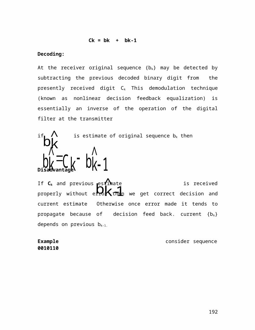
Chip duration =hop duration Chip duration=bit duration.
Fig. illustrates the variation of the frequency of a slow FH/MFSK signal with time
for one complete period of the PN sequence. The period of the PN sequence is
24-1 = 15. The FH/MFSK signal has the following parameters:
Number of bits per MFSK symbol K = 2.
Number of MFSK tones M = 2K = 4
Length of PN segment per hop k = 3
Total number of frequency hops 2k = 8
192

Fig. illustrates the variation of the transmitted frequency of a fast FH/MFSK signal
with time. The signal has the following parameters:
Number of bits per MFSK symbol K = 2.
Number of MFSK tones M = 2K = 4
Length of PN segment per hop k = 3
Total number of frequency hops 2k = 8
193

194