Embed Size (px)
Citation preview

This is preliminary information on a new product foreseen to be developed. Details are subject to change without notice.
November 2013 DocID025603 Rev 1 1/66
LSM6DB0
iNEMO advanced inertial module: 3D accelerometer, 3D gyroscope and signal processor
Datasheet - target specification
Features Motion sensors:
– ±2/±4/±8 g full scale– ±245/±500/±2000 dps full scale– 6-axis eco power mode down to 1.8 mA– 3 independent acceleration channels and
3 angular rate channels– Embedded temperature sensor– 20 Kbyte data batching – 6-axis and 9-axis quaternions– Self-test– ECOPACK®, RoHS and “Green” compliant
Signal processor:– Brain: ARM-based, 32-bit Cortex-M0 core– Flash memory and SRAM including a bank
with error code correction (ECC)– I2C master port – I2C slave port– SPI master/slave– 4-wire UART– 11 programmable GPIOs– Low-power features– 8 x 32-bit dual timers, watchdog timer
(WDG), Cortex-M0 system tick (SysTick) timer
– Standard 4-wire JTAG and 2-wire SWD– 80 MHz / 32 kHz RC / up to 80 MHz from
single-ended external clock
Applications Sensor hubs and sensor fusion Significant motion-detection and gesture
recognition Gaming and geomagnetic rotation vectors Pedometers, step counters and step detectors Calibrated compasses Enhanced navigation and motion tracking
Description The LSM6DB0 is an advanced low-power high-performance smart sensor system available in a plastic 3x3x1 mm LGA (land grid array) package. The module includes a three-axis accelerometer, 3-axis gyroscope and Cortex-M0 core with Flash, SRAM, dual timers, 2 I2C (master/slave), 1 SPI (master/slave) and 1 UART (transmitter/receiver).
The LSM6DB0 has a full-scale acceleration range of ±2/±4/±8 g and an angular rate range of ±245/±500/±2000 dps. The LSM6DB0 has two operating modes in that the accelerometer and gyroscope sensors can be either activated at the same ODR or the accelerometer can be enabled while the gyroscope is in power-down.
The module collects inputs from the accelerometer, gyroscope, compass and several other sensors and elaborates/fuses together 9 or 10 axes (iNemo Engine software) which are provided to the main application processor. For example, quaternions achieve the best compromise in terms of power saving for the overall system. The LSM6DB0 is fully compliant with the Android Kitkat OS.
LGA-22 (3x3x1 mm)
Table 1. Device summary
Order codes Temp. range [°C] Package Packaging
LSM6DB0 -40 to +85 LGA-22 Tray
LSM6DB0TR -40 to +85 LGA-22 Tape and reel
www.st.com

Contents LSM6DB0
2/66 DocID025603 Rev 1
Contents
1 Block diagrams and pin description . . . . . . . . . . . . . . . . . . . . . . . . . . . 101.1 Block diagrams . . . . . . . . . . . . . . . . . . . . . . . . . . . . . . . . . . . . . . . . . . . . . 10
1.2 Pin description . . . . . . . . . . . . . . . . . . . . . . . . . . . . . . . . . . . . . . . . . . . . . 12
2 LSM6DB0 features . . . . . . . . . . . . . . . . . . . . . . . . . . . . . . . . . . . . . . . . . . 14
3 Mechanical characteristics . . . . . . . . . . . . . . . . . . . . . . . . . . . . . . . . . . . 153.1 Accelerometer and gyroscope mechanical characteristics . . . . . . . . . . . . 15
3.2 Accelerometer and gyroscope electrical characteristics . . . . . . . . . . . . . . 16
3.3 Microprocessor electrical characteristics . . . . . . . . . . . . . . . . . . . . . . . . . 17
3.4 Temperature sensor characteristics . . . . . . . . . . . . . . . . . . . . . . . . . . . . . 18
4 Motion sensor communication interface characteristics . . . . . . . . . . 194.1 I2C - inter-IC control interface . . . . . . . . . . . . . . . . . . . . . . . . . . . . . . . . . . 19
5 Terminology . . . . . . . . . . . . . . . . . . . . . . . . . . . . . . . . . . . . . . . . . . . . . . . 205.1 Sensitivity . . . . . . . . . . . . . . . . . . . . . . . . . . . . . . . . . . . . . . . . . . . . . . . . . 20
5.2 Zero-g and zero rate level . . . . . . . . . . . . . . . . . . . . . . . . . . . . . . . . . . . . 20
6 Device operating modes . . . . . . . . . . . . . . . . . . . . . . . . . . . . . . . . . . . . . 216.1 Accelerometer and gyroscope operating modes . . . . . . . . . . . . . . . . . . . 21
6.2 Gyroscope power modes . . . . . . . . . . . . . . . . . . . . . . . . . . . . . . . . . . . . . 21
6.3 Microprocessor operating modes . . . . . . . . . . . . . . . . . . . . . . . . . . . . . . . 23
7 Accelerometer and gyroscope functionality . . . . . . . . . . . . . . . . . . . . . 257.1 Multiple reads (burst) . . . . . . . . . . . . . . . . . . . . . . . . . . . . . . . . . . . . . . . . 25
7.2 FIFO . . . . . . . . . . . . . . . . . . . . . . . . . . . . . . . . . . . . . . . . . . . . . . . . . . . . . 257.2.1 Bypass mode . . . . . . . . . . . . . . . . . . . . . . . . . . . . . . . . . . . . . . . . . . . . . 26
7.2.2 FIFO mode . . . . . . . . . . . . . . . . . . . . . . . . . . . . . . . . . . . . . . . . . . . . . . . 26
7.2.3 Continuous mode . . . . . . . . . . . . . . . . . . . . . . . . . . . . . . . . . . . . . . . . . . 27
7.2.4 Continuous-to-FIFO mode . . . . . . . . . . . . . . . . . . . . . . . . . . . . . . . . . . . 28
7.2.5 Bypass-to-Continuous mode . . . . . . . . . . . . . . . . . . . . . . . . . . . . . . . . . 29
DocID025603 Rev 1 3/66
LSM6DB0 Contents
66
8 Microprocessor functionality . . . . . . . . . . . . . . . . . . . . . . . . . . . . . . . . . 308.1 ARM Cortex-M0 core . . . . . . . . . . . . . . . . . . . . . . . . . . . . . . . . . . . . . . . . 30
8.1.1 Nested vectored interrupt controller (NVIC) . . . . . . . . . . . . . . . . . . . . . . 30
8.2 Power supply scheme . . . . . . . . . . . . . . . . . . . . . . . . . . . . . . . . . . . . . . . 30
8.3 Reset management . . . . . . . . . . . . . . . . . . . . . . . . . . . . . . . . . . . . . . . . . 31
8.4 Boot mode . . . . . . . . . . . . . . . . . . . . . . . . . . . . . . . . . . . . . . . . . . . . . . . . 31
8.5 Clock management . . . . . . . . . . . . . . . . . . . . . . . . . . . . . . . . . . . . . . . . . 31
8.6 General-purpose inputs/outputs (GPIOs) . . . . . . . . . . . . . . . . . . . . . . . . . 33
8.7 Memories . . . . . . . . . . . . . . . . . . . . . . . . . . . . . . . . . . . . . . . . . . . . . . . . . 33
8.8 Timers and watchdogs . . . . . . . . . . . . . . . . . . . . . . . . . . . . . . . . . . . . . . . 348.8.1 Dual timer . . . . . . . . . . . . . . . . . . . . . . . . . . . . . . . . . . . . . . . . . . . . . . . 34
8.8.2 Watchdog (WDG) timer . . . . . . . . . . . . . . . . . . . . . . . . . . . . . . . . . . . . . 34
8.8.3 System tick (SysTick) timer . . . . . . . . . . . . . . . . . . . . . . . . . . . . . . . . . . 34
8.9 Communication interfaces . . . . . . . . . . . . . . . . . . . . . . . . . . . . . . . . . . . . 35
8.10 I²C bus . . . . . . . . . . . . . . . . . . . . . . . . . . . . . . . . . . . . . . . . . . . . . . . . . . . 35
8.11 Universal asynchronous receiver transmitter (UART) . . . . . . . . . . . . . . . 35
8.12 Serial peripheral interface (SPI) . . . . . . . . . . . . . . . . . . . . . . . . . . . . . . . . 35
8.13 JTAG and SW debug support . . . . . . . . . . . . . . . . . . . . . . . . . . . . . . . . . . 36
9 Absolute maximum ratings . . . . . . . . . . . . . . . . . . . . . . . . . . . . . . . . . . 379.1 Accelerometer and gyroscope . . . . . . . . . . . . . . . . . . . . . . . . . . . . . . . . . 37
9.2 Microprocessor . . . . . . . . . . . . . . . . . . . . . . . . . . . . . . . . . . . . . . . . . . . . . 37
10 Register mapping . . . . . . . . . . . . . . . . . . . . . . . . . . . . . . . . . . . . . . . . . . 38
11 Register description . . . . . . . . . . . . . . . . . . . . . . . . . . . . . . . . . . . . . . . . 4011.1 INT_GEN_CFG2_XL (01h) . . . . . . . . . . . . . . . . . . . . . . . . . . . . . . . . . . . 40
11.2 INT_GEN_THS2_XL (02h) . . . . . . . . . . . . . . . . . . . . . . . . . . . . . . . . . . . . 41
11.3 INT_GEN_DUR2_XL (03h) . . . . . . . . . . . . . . . . . . . . . . . . . . . . . . . . . . . 41
11.4 ACT_THS (04h) . . . . . . . . . . . . . . . . . . . . . . . . . . . . . . . . . . . . . . . . . . . . 41
11.5 ACT_DUR (05h) . . . . . . . . . . . . . . . . . . . . . . . . . . . . . . . . . . . . . . . . . . . . 41
11.6 INT_GEN_CFG1_XL (06h) . . . . . . . . . . . . . . . . . . . . . . . . . . . . . . . . . . . 42
11.7 INT_GEN_THS1_X_XL (07h) . . . . . . . . . . . . . . . . . . . . . . . . . . . . . . . . . 42
11.8 INT_GEN_THS1_Y_XL (08h) . . . . . . . . . . . . . . . . . . . . . . . . . . . . . . . . . 43

Contents LSM6DB0
4/66 DocID025603 Rev 1
11.9 INT_GEN_THS1_Z_XL (09h) . . . . . . . . . . . . . . . . . . . . . . . . . . . . . . . . . . 43
11.10 INT_GEN_DUR1_XL (0Ah) . . . . . . . . . . . . . . . . . . . . . . . . . . . . . . . . . . . 43
11.11 REFERENCE_G (0Bh) . . . . . . . . . . . . . . . . . . . . . . . . . . . . . . . . . . . . . . . 43
11.12 INT1_CTRL (0Ch) . . . . . . . . . . . . . . . . . . . . . . . . . . . . . . . . . . . . . . . . . . 44
11.13 INT2_CTRL (0Dh) . . . . . . . . . . . . . . . . . . . . . . . . . . . . . . . . . . . . . . . . . . 44
11.14 WHO_AM_I (0Fh) . . . . . . . . . . . . . . . . . . . . . . . . . . . . . . . . . . . . . . . . . . . 45
11.15 CTRL_REG1_G (10h) . . . . . . . . . . . . . . . . . . . . . . . . . . . . . . . . . . . . . . . 45
11.16 CTRL_REG2_G (11h) . . . . . . . . . . . . . . . . . . . . . . . . . . . . . . . . . . . . . . . 48
11.17 CTRL_REG3_G (12h) . . . . . . . . . . . . . . . . . . . . . . . . . . . . . . . . . . . . . . . 48
11.18 ORIENT_CFG_G (13h) . . . . . . . . . . . . . . . . . . . . . . . . . . . . . . . . . . . . . . 49
11.19 INT_GEN_SRC_G (14h) . . . . . . . . . . . . . . . . . . . . . . . . . . . . . . . . . . . . . 49
11.20 OUT_TEMP_L (15h), OUT_TEMP_H (16h) . . . . . . . . . . . . . . . . . . . . . . . 50
11.21 STATUS_REG (17h) . . . . . . . . . . . . . . . . . . . . . . . . . . . . . . . . . . . . . . . . . 50
11.22 OUT_X_G (18h - 19h) . . . . . . . . . . . . . . . . . . . . . . . . . . . . . . . . . . . . . . . 51
11.23 OUT_Y_G (1Ah - 1Bh) . . . . . . . . . . . . . . . . . . . . . . . . . . . . . . . . . . . . . . . 51
11.24 OUT_Z_G (1Ch - 1Dh) . . . . . . . . . . . . . . . . . . . . . . . . . . . . . . . . . . . . . . . 51
11.25 CTRL_REG4 (1Eh) . . . . . . . . . . . . . . . . . . . . . . . . . . . . . . . . . . . . . . . . . 51
11.26 CTRL_REG5_XL (1Fh) . . . . . . . . . . . . . . . . . . . . . . . . . . . . . . . . . . . . . . 52
11.27 CTRL_REG6_XL (20h) . . . . . . . . . . . . . . . . . . . . . . . . . . . . . . . . . . . . . . 52
11.28 CTRL_REG7_XL (21h) . . . . . . . . . . . . . . . . . . . . . . . . . . . . . . . . . . . . . . 53
11.29 CTRL_REG8 (22h) . . . . . . . . . . . . . . . . . . . . . . . . . . . . . . . . . . . . . . . . . . 54
11.30 CTRL_REG9 (23h) . . . . . . . . . . . . . . . . . . . . . . . . . . . . . . . . . . . . . . . . . . 55
11.31 CTRL_REG10 (24h) . . . . . . . . . . . . . . . . . . . . . . . . . . . . . . . . . . . . . . . . . 55
11.32 INT_GEN_SRC_XL (26h) . . . . . . . . . . . . . . . . . . . . . . . . . . . . . . . . . . . . 56
11.33 STATUS_REG (27h) . . . . . . . . . . . . . . . . . . . . . . . . . . . . . . . . . . . . . . . . . 56
11.34 OUT_X_XL (28h - 29h) . . . . . . . . . . . . . . . . . . . . . . . . . . . . . . . . . . . . . . 57
11.35 OUT_Y_XL (2Ah - 2Bh) . . . . . . . . . . . . . . . . . . . . . . . . . . . . . . . . . . . . . . 57
11.36 OUT_Z_XL (2Ch - 2Dh) . . . . . . . . . . . . . . . . . . . . . . . . . . . . . . . . . . . . . . 57
11.37 FIFO_CTRL (2Eh) . . . . . . . . . . . . . . . . . . . . . . . . . . . . . . . . . . . . . . . . . . 57
11.38 FIFO_SRC (2Fh) . . . . . . . . . . . . . . . . . . . . . . . . . . . . . . . . . . . . . . . . . . . 58
11.39 INT_GEN_CFG_G (30h) . . . . . . . . . . . . . . . . . . . . . . . . . . . . . . . . . . . . . 58
11.40 INT_GEN_THS_X_G (31h - 32h) . . . . . . . . . . . . . . . . . . . . . . . . . . . . . . . 59
11.41 INT_GEN_THS_Y_G (33h - 34h) . . . . . . . . . . . . . . . . . . . . . . . . . . . . . . . 60

DocID025603 Rev 1 5/66
LSM6DB0 Contents
66
11.42 INT_GEN_THS_Z_G (35h - 36h) . . . . . . . . . . . . . . . . . . . . . . . . . . . . . . . 60
11.43 INT_GEN_DUR_G (37h) . . . . . . . . . . . . . . . . . . . . . . . . . . . . . . . . . . . . . 60
12 Soldering information . . . . . . . . . . . . . . . . . . . . . . . . . . . . . . . . . . . . . . . 63
13 Package information . . . . . . . . . . . . . . . . . . . . . . . . . . . . . . . . . . . . . . . . 64
14 Revision history . . . . . . . . . . . . . . . . . . . . . . . . . . . . . . . . . . . . . . . . . . . 65

List of tables LSM6DB0
6/66 DocID025603 Rev 1
List of tables
Table 1. Device summary . . . . . . . . . . . . . . . . . . . . . . . . . . . . . . . . . . . . . . . . . . . . . . . . . . . . . . . . . . 1Table 2. Pin description . . . . . . . . . . . . . . . . . . . . . . . . . . . . . . . . . . . . . . . . . . . . . . . . . . . . . . . . . . 12Table 3. Mechanical characteristics . . . . . . . . . . . . . . . . . . . . . . . . . . . . . . . . . . . . . . . . . . . . . . . . . 15Table 4. Electrical characteristics . . . . . . . . . . . . . . . . . . . . . . . . . . . . . . . . . . . . . . . . . . . . . . . . . . . 16Table 5. DC and AC parameters. . . . . . . . . . . . . . . . . . . . . . . . . . . . . . . . . . . . . . . . . . . . . . . . . . . . 17Table 6. Temperature sensor characteristics . . . . . . . . . . . . . . . . . . . . . . . . . . . . . . . . . . . . . . . . . . 18Table 7. I2C slave timing values . . . . . . . . . . . . . . . . . . . . . . . . . . . . . . . . . . . . . . . . . . . . . . . . . . . . 19Table 8. Gyroscope operating mode. . . . . . . . . . . . . . . . . . . . . . . . . . . . . . . . . . . . . . . . . . . . . . . . . 22Table 9. Operating mode current consumption. . . . . . . . . . . . . . . . . . . . . . . . . . . . . . . . . . . . . . . . . 22Table 10. Gyroscope turn-on time . . . . . . . . . . . . . . . . . . . . . . . . . . . . . . . . . . . . . . . . . . . . . . . . . . . 22Table 11. Accelerometer turn-on time. . . . . . . . . . . . . . . . . . . . . . . . . . . . . . . . . . . . . . . . . . . . . . . . . 23Table 12. LSM6DB0 operating modes . . . . . . . . . . . . . . . . . . . . . . . . . . . . . . . . . . . . . . . . . . . . . . . . 24Table 13. Alternate function input/output . . . . . . . . . . . . . . . . . . . . . . . . . . . . . . . . . . . . . . . . . . . . . . 33Table 14. Debug mode selection . . . . . . . . . . . . . . . . . . . . . . . . . . . . . . . . . . . . . . . . . . . . . . . . . . . . 36Table 15. Absolute maximum ratings . . . . . . . . . . . . . . . . . . . . . . . . . . . . . . . . . . . . . . . . . . . . . . . . . 37Table 16. Absolute maximum ratings for microprocessor. . . . . . . . . . . . . . . . . . . . . . . . . . . . . . . . . . 37Table 17. Motion sensor registers. . . . . . . . . . . . . . . . . . . . . . . . . . . . . . . . . . . . . . . . . . . . . . . . . . . . 38Table 18. INT_GEN_CFG2_XL register . . . . . . . . . . . . . . . . . . . . . . . . . . . . . . . . . . . . . . . . . . . . . . . 40Table 19. INT_GEN_CFG2_XL register description . . . . . . . . . . . . . . . . . . . . . . . . . . . . . . . . . . . . . . 40Table 20. INT_GEN_THS2_XL register . . . . . . . . . . . . . . . . . . . . . . . . . . . . . . . . . . . . . . . . . . . . . . . 41Table 21. INT_GEN_THS2_XL register description . . . . . . . . . . . . . . . . . . . . . . . . . . . . . . . . . . . . . . 41Table 22. INT_GEN_DUR2_XL register . . . . . . . . . . . . . . . . . . . . . . . . . . . . . . . . . . . . . . . . . . . . . . . 41Table 23. INT_GEN_DUR2_XL register description. . . . . . . . . . . . . . . . . . . . . . . . . . . . . . . . . . . . . . 41Table 24. ACT_THS register. . . . . . . . . . . . . . . . . . . . . . . . . . . . . . . . . . . . . . . . . . . . . . . . . . . . . . . . 41Table 25. ACT_THS register description . . . . . . . . . . . . . . . . . . . . . . . . . . . . . . . . . . . . . . . . . . . . . . 41Table 26. ACT_DUR register . . . . . . . . . . . . . . . . . . . . . . . . . . . . . . . . . . . . . . . . . . . . . . . . . . . . . . . 41Table 27. ACT_DUR register description . . . . . . . . . . . . . . . . . . . . . . . . . . . . . . . . . . . . . . . . . . . . . . 41Table 28. INT_GEN_CFG1_XL register . . . . . . . . . . . . . . . . . . . . . . . . . . . . . . . . . . . . . . . . . . . . . . . 42Table 29. INT_GEN_CFG1_XL register description . . . . . . . . . . . . . . . . . . . . . . . . . . . . . . . . . . . . . . 42Table 30. INT_GEN_THS1_X_XL register . . . . . . . . . . . . . . . . . . . . . . . . . . . . . . . . . . . . . . . . . . . . . 42Table 31. INT_GEN_THS1_X_XL register description . . . . . . . . . . . . . . . . . . . . . . . . . . . . . . . . . . . . 42Table 32. INT_GEN_THS1_Y_XL register . . . . . . . . . . . . . . . . . . . . . . . . . . . . . . . . . . . . . . . . . . . . . 43Table 33. INT_GEN_THS1_Y_XL register description . . . . . . . . . . . . . . . . . . . . . . . . . . . . . . . . . . . . 43Table 34. INT_GEN_THS1_Z_XL register . . . . . . . . . . . . . . . . . . . . . . . . . . . . . . . . . . . . . . . . . . . . . 43Table 35. INT_GEN_THS_Z_XL register description . . . . . . . . . . . . . . . . . . . . . . . . . . . . . . . . . . . . . 43Table 36. INT_GEN_DUR1_XL register . . . . . . . . . . . . . . . . . . . . . . . . . . . . . . . . . . . . . . . . . . . . . . . 43Table 37. INT_GEN_DUR1_XL register description. . . . . . . . . . . . . . . . . . . . . . . . . . . . . . . . . . . . . . 43Table 38. REFERENCE_G register . . . . . . . . . . . . . . . . . . . . . . . . . . . . . . . . . . . . . . . . . . . . . . . . . . 43Table 39. REFERENCE_G register description . . . . . . . . . . . . . . . . . . . . . . . . . . . . . . . . . . . . . . . . . 43Table 40. INT1_CTRL register . . . . . . . . . . . . . . . . . . . . . . . . . . . . . . . . . . . . . . . . . . . . . . . . . . . . . . 44Table 41. INT1_CTRL register description . . . . . . . . . . . . . . . . . . . . . . . . . . . . . . . . . . . . . . . . . . . . . 44Table 42. INT2_CTRL register . . . . . . . . . . . . . . . . . . . . . . . . . . . . . . . . . . . . . . . . . . . . . . . . . . . . . . 44Table 43. INT2_CTRL register description . . . . . . . . . . . . . . . . . . . . . . . . . . . . . . . . . . . . . . . . . . . . . 45Table 44. WHO_AM_I register . . . . . . . . . . . . . . . . . . . . . . . . . . . . . . . . . . . . . . . . . . . . . . . . . . . . . . 45Table 45. CTRL_REG1_G register . . . . . . . . . . . . . . . . . . . . . . . . . . . . . . . . . . . . . . . . . . . . . . . . . . . 45Table 46. CTRL_REG1_G register description. . . . . . . . . . . . . . . . . . . . . . . . . . . . . . . . . . . . . . . . . . 45Table 47. ODR and BW configuration setting (after LPF1). . . . . . . . . . . . . . . . . . . . . . . . . . . . . . . . . 46Table 48. ODR and BW configuration setting (after LPF2). . . . . . . . . . . . . . . . . . . . . . . . . . . . . . . . . 47

DocID025603 Rev 1 7/66
LSM6DB0 List of tables
66
Table 49. CTRL_REG2_G register . . . . . . . . . . . . . . . . . . . . . . . . . . . . . . . . . . . . . . . . . . . . . . . . . . . 48Table 50. CTRL_REG2_G register description. . . . . . . . . . . . . . . . . . . . . . . . . . . . . . . . . . . . . . . . . . 48Table 51. CTRL_REG3_G register . . . . . . . . . . . . . . . . . . . . . . . . . . . . . . . . . . . . . . . . . . . . . . . . . . . 48Table 52. CTRL_REG3_G register description. . . . . . . . . . . . . . . . . . . . . . . . . . . . . . . . . . . . . . . . . . 48Table 53. Gyroscope high-pass filter cutoff frequency configuration [Hz]. . . . . . . . . . . . . . . . . . . . . . 49Table 54. ORIENT_CFG_G register . . . . . . . . . . . . . . . . . . . . . . . . . . . . . . . . . . . . . . . . . . . . . . . . . . 49Table 55. ORIENT_CFG_G register description. . . . . . . . . . . . . . . . . . . . . . . . . . . . . . . . . . . . . . . . . 49Table 56. INT_GEN_SRC_G register . . . . . . . . . . . . . . . . . . . . . . . . . . . . . . . . . . . . . . . . . . . . . . . . . 49Table 57. INT_GEN_SRC_G register description. . . . . . . . . . . . . . . . . . . . . . . . . . . . . . . . . . . . . . . . 50Table 58. OUT_TEMP_L register . . . . . . . . . . . . . . . . . . . . . . . . . . . . . . . . . . . . . . . . . . . . . . . . . . . . 50Table 59. OUT_TEMP_H register. . . . . . . . . . . . . . . . . . . . . . . . . . . . . . . . . . . . . . . . . . . . . . . . . . . . 50Table 60. OUT_TEMP register description. . . . . . . . . . . . . . . . . . . . . . . . . . . . . . . . . . . . . . . . . . . . . 50Table 61. STATUS_REG register . . . . . . . . . . . . . . . . . . . . . . . . . . . . . . . . . . . . . . . . . . . . . . . . . . . 50Table 62. STATUS_REG register description. . . . . . . . . . . . . . . . . . . . . . . . . . . . . . . . . . . . . . . . . . . 51Table 63. CTRL_REG4 register . . . . . . . . . . . . . . . . . . . . . . . . . . . . . . . . . . . . . . . . . . . . . . . . . . . . . 51Table 64. CTRL_REG4 register description . . . . . . . . . . . . . . . . . . . . . . . . . . . . . . . . . . . . . . . . . . . . 52Table 65. CTRL_REG5_XL register . . . . . . . . . . . . . . . . . . . . . . . . . . . . . . . . . . . . . . . . . . . . . . . . . . 52Table 66. CTRL_REG5_XL register description. . . . . . . . . . . . . . . . . . . . . . . . . . . . . . . . . . . . . . . . . 52Table 67. CTRL_REG6_XL register . . . . . . . . . . . . . . . . . . . . . . . . . . . . . . . . . . . . . . . . . . . . . . . . . . 52Table 68. CTRL_REG6_XL register description. . . . . . . . . . . . . . . . . . . . . . . . . . . . . . . . . . . . . . . . . 53Table 69. ODR register setting (accelerometer only mode) . . . . . . . . . . . . . . . . . . . . . . . . . . . . . . . . 53Table 70. CTRL_REG7_XL register . . . . . . . . . . . . . . . . . . . . . . . . . . . . . . . . . . . . . . . . . . . . . . . . . . 53Table 71. CTRL_REG7_XL register description. . . . . . . . . . . . . . . . . . . . . . . . . . . . . . . . . . . . . . . . . 54Table 72. Low-pass cutoff frequency in high resolution mode (HR = 1) . . . . . . . . . . . . . . . . . . . . . . . 54Table 73. CTRL_REG8 register . . . . . . . . . . . . . . . . . . . . . . . . . . . . . . . . . . . . . . . . . . . . . . . . . . . . . 54Table 74. CTRL_REG8 register description . . . . . . . . . . . . . . . . . . . . . . . . . . . . . . . . . . . . . . . . . . . . 54Table 75. CTRL_REG9 register . . . . . . . . . . . . . . . . . . . . . . . . . . . . . . . . . . . . . . . . . . . . . . . . . . . . . 55Table 76. CTRL_REG9 register description . . . . . . . . . . . . . . . . . . . . . . . . . . . . . . . . . . . . . . . . . . . . 55Table 77. CTRL_REG10 register . . . . . . . . . . . . . . . . . . . . . . . . . . . . . . . . . . . . . . . . . . . . . . . . . . . . 55Table 78. CTRL_REG10 register description . . . . . . . . . . . . . . . . . . . . . . . . . . . . . . . . . . . . . . . . . . . 55Table 79. INT_GEN_SRC_XL register . . . . . . . . . . . . . . . . . . . . . . . . . . . . . . . . . . . . . . . . . . . . . . . . 56Table 80. INT_GEN_SRC_XL register description . . . . . . . . . . . . . . . . . . . . . . . . . . . . . . . . . . . . . . . 56Table 81. STATUS_REG register . . . . . . . . . . . . . . . . . . . . . . . . . . . . . . . . . . . . . . . . . . . . . . . . . . . . 56Table 82. STATUS_REG register description. . . . . . . . . . . . . . . . . . . . . . . . . . . . . . . . . . . . . . . . . . . 56Table 83. FIFO_CTRL register . . . . . . . . . . . . . . . . . . . . . . . . . . . . . . . . . . . . . . . . . . . . . . . . . . . . . 57Table 84. FIFO_CTRL register description. . . . . . . . . . . . . . . . . . . . . . . . . . . . . . . . . . . . . . . . . . . . . 57Table 85. FIFO mode selection. . . . . . . . . . . . . . . . . . . . . . . . . . . . . . . . . . . . . . . . . . . . . . . . . . . . . . 57Table 86. FIFO_SRC register . . . . . . . . . . . . . . . . . . . . . . . . . . . . . . . . . . . . . . . . . . . . . . . . . . . . . . 58Table 87. FIFO_SRC register description. . . . . . . . . . . . . . . . . . . . . . . . . . . . . . . . . . . . . . . . . . . . . . 58Table 88. FIFO_SRC example: OVR/FSS details . . . . . . . . . . . . . . . . . . . . . . . . . . . . . . . . . . . . . . . 58Table 89. INT_GEN_CFG_G register . . . . . . . . . . . . . . . . . . . . . . . . . . . . . . . . . . . . . . . . . . . . . . . . . 58Table 90. INT_GEN_CFG_G register description. . . . . . . . . . . . . . . . . . . . . . . . . . . . . . . . . . . . . . . . 59Table 91. INT_GEN_THS_XH_G register . . . . . . . . . . . . . . . . . . . . . . . . . . . . . . . . . . . . . . . . . . . . . 59Table 92. INT_GEN_THS_XL_G register . . . . . . . . . . . . . . . . . . . . . . . . . . . . . . . . . . . . . . . . . . . . . . 59Table 93. INT_GEN_THS_X_G register description. . . . . . . . . . . . . . . . . . . . . . . . . . . . . . . . . . . . . . 59Table 94. INT_GEN_THS_YH_G register . . . . . . . . . . . . . . . . . . . . . . . . . . . . . . . . . . . . . . . . . . . . . 60Table 95. INT_GEN_THS_YL_G register . . . . . . . . . . . . . . . . . . . . . . . . . . . . . . . . . . . . . . . . . . . . . . 60Table 96. INT_GEN_THS_Y_G register description. . . . . . . . . . . . . . . . . . . . . . . . . . . . . . . . . . . . . . 60Table 97. INT_GEN_THS_ZH_G register. . . . . . . . . . . . . . . . . . . . . . . . . . . . . . . . . . . . . . . . . . . . . . 60Table 98. INT_GEN_THS_ZL_G register . . . . . . . . . . . . . . . . . . . . . . . . . . . . . . . . . . . . . . . . . . . . . . 60Table 99. INT_GEN_THS_Z_G register description. . . . . . . . . . . . . . . . . . . . . . . . . . . . . . . . . . . . . . 60Table 100. INT_GEN_DUR_G register. . . . . . . . . . . . . . . . . . . . . . . . . . . . . . . . . . . . . . . . . . . . . . . . . 60

List of tables LSM6DB0
8/66 DocID025603 Rev 1
Table 101. INT_GEN_DUR_G register description . . . . . . . . . . . . . . . . . . . . . . . . . . . . . . . . . . . . . . . 61Table 102. Document revision history. . . . . . . . . . . . . . . . . . . . . . . . . . . . . . . . . . . . . . . . . . . . . . . . . . 65

DocID025603 Rev 1 9/66
LSM6DB0 List of figures
66
List of figures
Figure 1. LSM6DB0 application block diagram . . . . . . . . . . . . . . . . . . . . . . . . . . . . . . . . . . . . . . . . . 10Figure 2. Accelerometer and gyroscope block diagram. . . . . . . . . . . . . . . . . . . . . . . . . . . . . . . . . . . 11Figure 3. Microprocessor block diagram . . . . . . . . . . . . . . . . . . . . . . . . . . . . . . . . . . . . . . . . . . . . . . 11Figure 4. Pin connections . . . . . . . . . . . . . . . . . . . . . . . . . . . . . . . . . . . . . . . . . . . . . . . . . . . . . . . . . 12Figure 5. I2C slave timing diagram. . . . . . . . . . . . . . . . . . . . . . . . . . . . . . . . . . . . . . . . . . . . . . . . . . . 19Figure 6. Switching operating modes. . . . . . . . . . . . . . . . . . . . . . . . . . . . . . . . . . . . . . . . . . . . . . . . . 21Figure 7. Multiple reads: accelerometer only . . . . . . . . . . . . . . . . . . . . . . . . . . . . . . . . . . . . . . . . . . . 25Figure 8. Multiple reads: accelerometer and gyroscope . . . . . . . . . . . . . . . . . . . . . . . . . . . . . . . . . . 25Figure 9. Bypass mode . . . . . . . . . . . . . . . . . . . . . . . . . . . . . . . . . . . . . . . . . . . . . . . . . . . . . . . . . . . 26Figure 10. FIFO mode . . . . . . . . . . . . . . . . . . . . . . . . . . . . . . . . . . . . . . . . . . . . . . . . . . . . . . . . . . . . . 27Figure 11. Continuous mode . . . . . . . . . . . . . . . . . . . . . . . . . . . . . . . . . . . . . . . . . . . . . . . . . . . . . . . . 27Figure 12. Continuous-to-FIFO mode . . . . . . . . . . . . . . . . . . . . . . . . . . . . . . . . . . . . . . . . . . . . . . . . . 28Figure 13. Bypass-to-Continuous mode. . . . . . . . . . . . . . . . . . . . . . . . . . . . . . . . . . . . . . . . . . . . . . . . 29Figure 14. LSM6DB0 digital power supply generation. . . . . . . . . . . . . . . . . . . . . . . . . . . . . . . . . . . . . 30Figure 15. Clock tree . . . . . . . . . . . . . . . . . . . . . . . . . . . . . . . . . . . . . . . . . . . . . . . . . . . . . . . . . . . . . . 31Figure 16. Debug mode selection timing . . . . . . . . . . . . . . . . . . . . . . . . . . . . . . . . . . . . . . . . . . . . . . . 36Figure 17. INT_SEL and OUT_SEL configuration gyroscope block diagram . . . . . . . . . . . . . . . . . . . 48Figure 18. Wait bit disabled . . . . . . . . . . . . . . . . . . . . . . . . . . . . . . . . . . . . . . . . . . . . . . . . . . . . . . . . . 61Figure 19. Wait bit enabled . . . . . . . . . . . . . . . . . . . . . . . . . . . . . . . . . . . . . . . . . . . . . . . . . . . . . . . . . 62Figure 20. LGA-22: mechanical data and package dimensions. . . . . . . . . . . . . . . . . . . . . . . . . . . . . . 64

Block diagrams and pin description LSM6DB0
10/66 DocID025603 Rev 1
1 Block diagrams and pin description
1.1 Block diagramsThe LSM6DB0 includes a 3-axis accelerometer and 3-axis gyroscope combined with a low-power microprocessor ARM-based Cortex-M0. The reference block diagram is described in Figure 1 while the motion sensor and microprocessor block diagrams are described in Figure 2 and Figure 3, respectively.
Figure 1. LSM6DB0 application block diagram
Magnetometer
Pressure sensor
Other sensors
Accelerometer and Gyroscope
FIFOs
BRAIN
ARM Cortex-M0
RAM Data Fusion Algorithms
Application Processor
I2C
I2C
I2C
INT INT
LSM6DB0
INT1 INT2DIO7DIO8
DIO12 DIO11

DocID025603 Rev 1 11/66
LSM6DB0 Block diagrams and pin description
66
Figure 2. Accelerometer and gyroscope block diagram
Figure 3. Microprocessor block diagram
Legend: NVIC = nested vectored interrupt controller, GPIO = general-purpose input/output
CHARGEAMPLIFIER
Y+
Z+
Y-
Z-
aX+
X-
MUX
x,y,z
Y+
Z+
Y-
Z-
X+
X-
MUX
ADC LPF1 1
0
HP_EN
LPF2
HPF
Data Reg
InterruptGenerator
I2CSPI
OUT_SEL
INT_SEL
SRC Registers
CFG Registers
Gyro
FIFO
LPF1 ADC
1
0
HPF
HPIS1
FDS
XL
Gyro
LPF2
HR
InterruptGenerator
XL
0
0
1
1
XL
XL
XL
Gyro Gyro
Gyro
+Ω

Block diagrams and pin description LSM6DB0
12/66 DocID025603 Rev 1
1.2 Pin description
Figure 4. Pin connections
Table 2. Pin description Pin# Name Function I/O level
1 VDD1.8 Power supply for I/O pins
2 DIO0 GPIO0 / SW_TDIO / JTAG TMS / UART_CTS VDD1.8
3 DIO1 GPIO1 / SW_TCK / JTAG TCK / UART_RTS VDD1.8
4 DIO2 GPIO2 / I2C2_SCL (slave) / UART_TXD VDD1.8
5 RESET Microcontroller reset VDD
6 DIO3 GPIO3 / I2C2_SDA (slave) / UART_RXD VDD1.8
7 DIO4 GPIO4 / JTAG TDO VDD1.8
8 DIO5 GPIO5 / JTAG TDI / Clock input VDD1.8
9 DIO8 GPIO8 / I2C1_SDA (master) / SPI_OUT VDD
10 DIO6 GPIO6 / 16 MHz clock output / Clock 32KHz VDD
11 DIO7 GPIO7 / I2C1_SCL (master) / SPI_Clock VDD
12 GND 0 V supply
13 LD01.2 Connect to decoupling capacitor for 1.2 V digital regulator to GND
14 VDD(1) Analog and I/O pins power supply
(TOP VIEW)DIRECTIONS OF THE DETECTABLE ANGULAR RATES
X
Z
X
Y
(TOP VIEW)DIRECTION OF THE DETECTABLE ACCELERATIONS
VDD1.8DIO0DIO1DIO2
GND
DIO
8
DIO
4
RESET
DIO
6
1
10 7
5
16
LDO1.2VDD
DIO10DIO9
6
DIO
5
11
17 20
RES
CAP
RES
RES
BOTTOM VIEW
2122
DIO3DIO7
RES RES
+Ω
+Ω
+Ω
Y
X
Z

DocID025603 Rev 1 13/66
LSM6DB0 Block diagrams and pin description
66
15 DIO10 GPIO10 / spi_input VDD
16 DIO9 GPIO9 / SPI_CS VDD
17 RES Connect to GND
18 RES Connect to GND
19 RES Connect to VDD
20 CAP Connect to GND with ceramic capacitor(2)
21 RES Leave unconnected
22 RES Leave unconnected
1. Recommended 100 nF filter capacitor.
2. 10 nF (±10%), 16 V. 1 nF minimum value has to be guaranteed under 12 V bias condition.
The INT1 and INT2 pins of the motion sensor are internally connected to the DIO12 and DIO11 pins of the microcontroller, refer to Figure 1.
Table 2. Pin description (continued)Pin# Name Function I/O level

LSM6DB0 features LSM6DB0
14/66 DocID025603 Rev 1
2 LSM6DB0 features
In the LSM6DB0 a complete sensor networking has been created with three additional external sensor connections supported by the I2C bus (eg. compass, pressure sensors, others). External data acquisition is totally configurable with a different data rate selection and different data reads for each slave sensor. To minimize the core’s (Brain) power consumption, dedicated FIFO buffers are available in the inertial sensors to maximize the temporary data storage.
The LSM6DB0 can manage standard hub functionalities together with the implementation of complex algorithms for the following applications:
– Sensor batching with combination of sensors based on different ODR and related time-stamp information;
– Sensor fusion with the support of quaternions, gravity, linear acceleration and orientation data;
– Pedometers;– Game rotation vectors;– Geomagnetic rotation vectors (3-axis accelerometer and 3-axis magnetometer);– Compass calibration;– Gyroscope bias estimation and offset compensation;– Accelerometer background calibration;– Significant motion;– Gesture recognition;
The device provides optimal flexibility, modularity and scalability in the customization of software routines for the customer.
The LSM6DB0 completely offloads the application processor from the computation of sensor fusion, delivering unparalleled low-power consumption at the system level. Owing to the embedded core (Brain) in the device, there is no need for an external processing unit nor storage.
The LSM6DB0 is compliant with Android Kitkat OS.
DocID025603 Rev 1 15/66
LSM6DB0 Mechanical characteristics
66
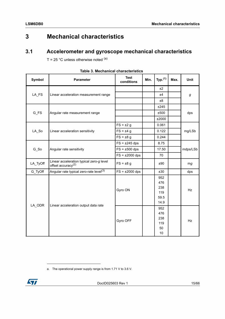
3 Mechanical characteristics
3.1 Accelerometer and gyroscope mechanical characteristicsT = 25 °C unless otherwise noted (a)
a. The operational power supply range is from 1.71 V to 3.6 V.
Table 3. Mechanical characteristics
Symbol Parameter Test conditions Min. Typ.(1) Max. Unit
LA_FS Linear acceleration measurement range
±2
g±4
±8
G_FS Angular rate measurement range
±245
dps±500
±2000
LA_So Linear acceleration sensitivity
FS = ±2 g 0.061
mg/LSbFS = ±4 g 0.122
FS = ±8 g 0.244
G_So Angular rate sensitivity
FS = ±245 dps 8.75
mdps/LSbFS = ±500 dps 17.50
FS = ±2000 dps 70
LA_TyOff Linear acceleration typical zero-g level offset accuracy(2) FS = ±8 g ±90 mg
G_TyOff Angular rate typical zero-rate level(3) FS = ±2000 dps ±30 dps
LA_ODR Linear acceleration output data rate
Gyro ON
95247623811959.514.9
Hz
Gyro OFF
9524762381195010
Hz

Mechanical characteristics LSM6DB0
16/66 DocID025603 Rev 1
3.2 Accelerometer and gyroscope electrical characteristicsT = 25 °C unless otherwise noted
Table 4. Electrical characteristics
G_ODR Angular digital output data rate
95247623811959.514.9
Hz
Top Operating temperature range -40 +85 °C
1. Typical specifications are not guaranteed.
2. Typical zero-g level offset value after soldering.
3. Typical zero-rate level offset value after MSL3 preconditioning.
Table 3. Mechanical characteristics (continued)
Symbol Parameter Test conditions Min. Typ.(1) Max. Unit
Symbol Parameter Test conditions Min. Typ.(1) Max. Unit
VDD Core and I/O pins supply voltage 1.71 3.6 V
LA_Idd Accelerometer current consumption in normal mode
ODR = 10 Hz 60
μAODR = 50 Hz 160
ODR 119 Hz 330
G_Idd Gyroscope current consumption in eco power mode 1.8 mA
Top Operating temperature range -40 +85 °C
1. Typical specifications are not guaranteed.

DocID025603 Rev 1 17/66
LSM6DB0 Mechanical characteristics
66
3.3 Microprocessor electrical characteristicsCharacteristics measured in Table 5 are for recommended operating conditions unless otherwise specified. Typical values are in reference to TA = 25 C, VDD =1.8 V.
Table 5. DC and AC parameters
Symbol Parameter Test conditions Min. Typ. Max. Unit
VDDOperating supply voltage master serial port (DIO6 to DIO10)
1.71 3.6 V
VDD1.8 Operating supply voltage (DIO0 to DIO5) 1.75 1.8 1.95 V
Power consumption (Dhrystone without compiler options)
Isupply Supply current
Reset 50 nA
Active (CPU, Flash, and RAM) 20
mA
From RAM80 MHz (0.79 DMIPS/MHz)40 MHz (0.79 DMIPS/MHz)20 MHz (0.79 DMIPS/MHz)16 MHz (0.79 DMIPS/MHz)10 MHz (0.79 DMIPS/MHz)
10.35.953.853.482.9
From Flash80 MHz (0.3 DMIPS/MHz)40 MHz (0.43 DMIPS/MHz)20 MHz (0.56 DMIPS/MHz)16 MHz (0.79 DMIPS/MHz)10 MHz (0.79 DMIPS/MHz)
7.55.5
4.744.343.7
Digital input and output (1.8 V supply)
CIN(1) Port I/O capacitance 1.3 1.4 1.7 pF
RPD(1) Pull-down value 117 211 334 kW
TRISE(1) Rise time 0.1*VDD to 0.9*VDD, CL = 50 pF 10.3 19
nsTFALL
(1) Fall time 0.9*VDD to 0.1*VDD, CL = 50 pF 11 22
VIH(1) Logic high-level input voltage 0.65 VDD
VVIL
(1) Logic low-level input voltage 0.35 VDD
Digital input and output (3.3 V supply)
CIN(1) Port I/O capacitance 1.3 1.4 1.7 pF
RPD(1) Pull-down value 53 84 144
kWRPU
(1) Pull-up value 57 81 122
TRISE(1) Rise time 0.1*VDD to 0.9*VDD, CL = 50 pF 1.4 12
nsTFALL
(1) Fall time 0.9*VDD to 0.1*VDD, CL = 50 pF 1.5 12.5

Mechanical characteristics LSM6DB0
18/66 DocID025603 Rev 1
3.4 Temperature sensor characteristics@ Vdd = 3V, T = 25 °C unless otherwise noted (b)
VIH(1) Logic high-level input voltage 0.65 VDD
VVIL
(1) Logic low-level input voltage 0.35 VDD
TAOperating ambient temperature range
-40 85 °C
1. Guaranteed by design
b. The product is factory calibrated at 3.0 V.
Table 6. Temperature sensor characteristicsSymbol Parameter Test condition Min. Typ.(1) Max. Unit
TODR Temperature refresh rateGyro OFF(2) 50
HzGyro ON 59.5
TSen Temperature sensitivity(3) 16 LSB/°C
Top Operating temperature range -40 +85 °C
1. Typical specifications are not guaranteed.
2. When the accelerometer ODR is set to 10 Hz and the gyroscope block is turned off, the TODR value is 10 Hz.
3. The output of the temperature sensor is 0 (typ.) at 25 °C
DocID025603 Rev 1 19/66
LSM6DB0 Motion sensor communication interface characteristics
66
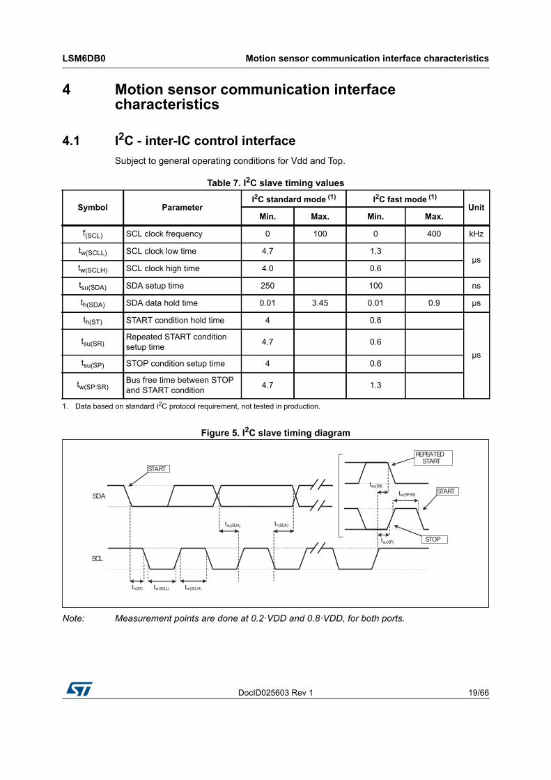
4 Motion sensor communication interface characteristics
4.1 I2C - inter-IC control interfaceSubject to general operating conditions for Vdd and Top.
Figure 5. I2C slave timing diagram
Note: Measurement points are done at 0.2·VDD and 0.8·VDD, for both ports.
Table 7. I2C slave timing values
Symbol ParameterI2C standard mode (1) I2C fast mode (1)
UnitMin. Max. Min. Max.
f(SCL) SCL clock frequency 0 100 0 400 kHz
tw(SCLL) SCL clock low time 4.7 1.3μs
tw(SCLH) SCL clock high time 4.0 0.6
tsu(SDA) SDA setup time 250 100 ns
th(SDA) SDA data hold time 0.01 3.45 0.01 0.9 μs
th(ST) START condition hold time 4 0.6
μstsu(SR)
Repeated START condition setup time 4.7 0.6
tsu(SP) STOP condition setup time 4 0.6
tw(SP:SR)Bus free time between STOP and START condition 4.7 1.3
1. Data based on standard I2C protocol requirement, not tested in production.
SDA
SCL
tsu(SP)
tw(SCLL)
tsu(SDA)
tsu(SR)
th(ST) tw(SCLH)
th(SDA)
tw(SP:SR)
START
REPEATEDSTART
STOP
START

Terminology LSM6DB0
20/66 DocID025603 Rev 1
5 Terminology
5.1 SensitivityLinear acceleration sensitivity can be determined, for example, by applying 1 g acceleration to the device. Because the sensor can measure DC accelerations, this can be done easily by pointing the selected axis towards the ground, noting the output value, rotating the sensor 180 degrees (pointing towards the sky) and noting the output value again. By doing so, ±1 g acceleration is applied to the sensor. Subtracting the larger output value from the smaller one, and dividing the result by 2, leads to the actual sensitivity of the sensor. This value changes very little over temperature and over time. The sensitivity tolerance describes the range of sensitivities of a large number of sensors.
An angular rate gyroscope is device that produces a positive-going digital output for counterclockwise rotation around the axis considered. Sensitivity describes the gain of the sensor and can be determined by applying a defined angular velocity to it. This value changes very little over temperature and time.
5.2 Zero-g and zero rate levelLinear acceleration zero-g level offset (TyOff) describes the deviation of an actual output signal from the ideal output signal if no acceleration is present. A sensor in a steady state on a horizontal surface will measure 0 g on both the X-axis and Y-axis, whereas the Z-axis will measure 1 g. Ideally, the output is in the middle of the dynamic range of the sensor (content of OUT registers 00h, data expressed as two’s complement number). A deviation from the ideal value in this case is called zero-g offset.
Offset is to some extent a result of stress to MEMS sensor and therefore the offset can slightly change after mounting the sensor onto a printed circuit board or exposing it to extensive mechanical stress. Offset changes little over temperature, see “Linear acceleration zero-g level change vs. temperature” in Table 3. The zero-g level tolerance (TyOff) describes the standard deviation of the range of zero-g levels of a group of sensors.
Zero-rate level describes the actual output signal if there is no angular rate present. The zero-rate level of precise MEMS sensors is, to some extent, a result of stress to the sensor and therefore the zero-rate level can slightly change after mounting the sensor onto a printed circuit board or after exposing it to extensive mechanical stress. This value changes very little over temperature and time.

DocID025603 Rev 1 21/66
LSM6DB0 Device operating modes
66
6 Device operating modes
6.1 Accelerometer and gyroscope operating modesThe LSM6DB0 has two operating modes available: only accelerometer active and gyroscope in power down or both accelerometer and gyroscope sensors active at the same ODR. Switching from one mode to the other requires one write operation: writing to CTRL_REG6_XL (20h) the accelerometer operates in normal mode and the gyroscope is powered down, writing to CTRL_REG1_G (10h) both the accelerometer and gyroscope are activated at the same ODR.
Figure 6 depicts both modes of operation from power down.
Figure 6. Switching operating modes
6.2 Gyroscope power modesIn the LSM6DB0, the gyroscope can be configured in three different operating modes: power-down, low-power and normal mode.
Low-power mode is available for lower ODR (14.9, 59.5, 119 Hz) while for greater ODR (238, 476, 952 Hz), the device is automatically in normal mode. Table 8 summarizes the ODR configuration (ODR_G[2:0] bits set in CTRL_REG1_G (10h)) and corresponding power modes.
To enable low-power mode, the LP_mode bit in CTRL_REG3_G (12h) has to be set to ‘1’.
Low-power mode allows reaching low power consumption while maintaining the device always on, refer to Table 9.
The turn-on time to change from all operating modes for the gyroscope and accelerometer is indicated in Table 10 and Table 11.
AccelerometerOnly
Accelerometer+
GyroPower Down
Write CTRL_REG1_G
Write CTRL_REG1_GWith CTRL_REG6_XL = PD
Write CTRL_REG6_XL

Device operating modes LSM6DB0
22/66 DocID025603 Rev 1
Table 8. Gyroscope operating modeODR_G [2:0] ODR [Hz] Power mode(1)
1. Gyroscope low-power mode is available for G_FS = ±2000 dps.
000 Power-down Power-down
001 14.9 Low-power
010 59.5 Low-power
011 119 Low-power
100 238 Normal mode
101 476 Normal mode
110 952 Normal mode
Table 9. Operating mode current consumption
ODR [Hz] Power modeCurrent consumption(1)
[mA]
1. Gyroscope and accelerometer current consumption typical values based on characterization data.
14.9 Low-power 1.8
59.5 Low-power 2.3
119 Low-power 2.9
238 Normal mode 4.3
476 Normal mode 4.3
952 Normal mode 4.3
Table 10. Gyroscope turn-on time
ODR [Hz] LPF1 only(1)
1. The table contains the number of samples to be discarded after switching between low-power mode and normal mode.
LPF1 and LPF2(1)
14.9 2 LPF2 not available
59.5 or 119 3 13
238 4 14
476 5 15
952 8 18

DocID025603 Rev 1 23/66
LSM6DB0 Device operating modes
66
6.3 Microprocessor operating modesSeveral microprocessor operating modes are defined for the LSM6DB0: Reset mode Two low-power modes: low-power wait-for-interrupt (WFI) mode and high-power wait-
for-interrupt (WFI) mode Active mode
In reset mode the LSM6DB0 is in ultra-low-power consumption: no voltage regulators, nor clocks are powered. The LSM6DB0 enters reset mode by asserting the external reset signal.
While in low-power WFI mode, the LSM6DB0 CPU is stopped and the high-frequency 80 MHz RC oscillator is powered down. All peripherals, apart from one timer, are disabled. The power consumption is about 800 μA with a 1 kHz clock.
In high-power WFI mode, the CPU is stopped and the high-frequency 80 MHz RC oscillator is powered up. This mode allows a faster response time for an interrupt to wake up the CPU. All peripherals are enabled and can wake up the CPU with an interrupt. The power consumption in this mode is around 2 mA with an 80 MHz clock.
In active mode the LSM6DB0 is fully operational: all interfaces, including SPI, I2C, JTAG and UART, are active as well as all internal power supplies together with the high-speed frequency oscillator. The MCU core is also running.
Table 11. Accelerometer turn-on time
ODR [Hz] BW = 400 Hz(1)
1. The table contains the number of samples to be discarded after switching between power-down mode and normal mode.
BW = 200 Hz(1) BW = 100 Hz(1) BW = 50 Hz(1)
14.9 0 0 0 0
59.5 0 0 0 0
119 1 1 1 2
238 1 1 2 4
476 1 2 4 7
952 2 4 7 14

Device operating modes LSM6DB0
24/66 DocID025603 Rev 1
Table 12 summarizes the modes of operation and transition times.
Table 12. LSM6DB0 operating modesIP Active mode High-power WFI mode Low-power WFI mode
CPU
Yes Yes
YesFlash
SRAM
BORYes
POR
High-speed internal osc. No
Low-speed internal osc. Yes
Timer Yes
SPI
NoI²C
UART
WDG Yes
GPIOs Yes
Wake-up time to active mode 0 μs 50 ns 300 μs
Consumption (typ) 10 mA 3 mA 800 μA

DocID025603 Rev 1 25/66
LSM6DB0 Accelerometer and gyroscope functionality
66
7 Accelerometer and gyroscope functionality
7.1 Multiple reads (burst)When only the accelerometer is activated and the gyroscope is in power down, starting from OUT_X_XL (28h - 29h) multiple reads can be performed. Once OUT_Z_XL (2Ch - 2Dh) is read, the system automatically restarts from OUT_X_XL (28h - 29h) (see Figure 7).
Figure 7. Multiple reads: accelerometer only
When both accelerometer and gyroscope sensors are activated at the same ODR, starting from OUT_X_G (18h - 19h) multiple reads can be performed. Once OUT_Z_XL (2Ch - 2Dh) is read, the system automatically restarts from OUT_X_G (18h - 19h) (see Figure 8).
Figure 8. Multiple reads: accelerometer and gyroscope
7.2 FIFOThe LSM6DB0 embeds a 32 slots of 16-bit data FIFO for each of the gyroscope’s three output channels, yaw, pitch and roll, and 16-bit data FIFO for each of the accelerometer’s three output channels, X, Y and Z. This allows consistent power saving for the system, since the host processor does not need to continuously poll data from the sensor, but it can wake up only when needed and burst the significant data out from the FIFO. This buffer can work accordingly to five different modes: Bypass mode, FIFO-mode, Continuous mode, Continuous-to-FIFO mode and Bypass-to-Continuous. Each mode is selected by the FMODE [2:0] bits in the FIFO_CTRL (2Eh) register. Programmable FIFO threshold status, FIFO overrun events and the number of unread samples stored are available in the FIFO_SRC (2Fh) register and can be set to generate dedicated interrupts on the INT1 pin using the INT1_CTRL (0Ch) register.
x,y,z OUT_Z_XLRead #1(2C-2D)(2A-2B)
OUT_Y_XL(28-29)OUT_X_XL
x,y,zRead #nOUT_Z_XL(2C-2D)(2A-2B)
OUT_Y_XL(28-29)OUT_X_XL
(15-16)OUT_TEMP
x,y,z OUT_Z_XLRead #1(2C-2D)(2A-2B)
OUT_Y_XL(28-29)OUT_X_XL
x,y,zRead #n
OUT_Z_G(1C-1D)(1A-1B)
OUT_Y_G(18-19)OUT_X_G
OUT_Z_XL(2C-2D)(2A-2B)
OUT_Y_XL(28-29)OUT_X_XLOUT_Z_G
(1C-1D)(1A-1B)OUT_Y_G
(18-19)OUT_X_G
(15-16)OUT_TEMP

Accelerometer and gyroscope functionality LSM6DB0
26/66 DocID025603 Rev 1
FIFO_SRC (2Fh) (FTH) goes to '1' when the number of unread samples (FIFO_SRC (2Fh) (FSS5:0)) is greater than or equal to FTH [4:0] in FIFO_CTRL (2Eh). If FIFO_CTRL (2Eh) (FTH[4:0]) is equal to 0, FIFO_SRC (2Fh) (FTH) goes to ‘0’.
FIFO_SRC (2Fh) (OVRN) is equal to '1' if a FIFO slot is overwritten.
FIFO_SRC (2Fh) (FSS [5:0]) contains stored data levels of unread samples. When FSS [5:0] is equal to ‘000000’, FIFO is empty, when FSS [5:0] is equal to ‘100000’, FIFO is full and the unread samples are 32.
The FIFO feature is enabled by writing '1' in CTRL_REG9 (23h) (FIFO_EN).
To guarantee the correct acquisition of data during the switching into and out of FIFO mode, the first sample acquired must be discarded.
7.2.1 Bypass modeIn Bypass mode (FIFO_CTRL (2Eh)(FMODE [2:0]= 000), the FIFO is not operational and it remains empty.
Bypass mode is also used to reset the FIFO when in FIFO mode.
As described in Figure 9, for each channel only the first address is used. When a new data is available the old data is overwritten.
Figure 9. Bypass mode
7.2.2 FIFO modeIn FIFO mode (FIFO_CTRL (2Eh) (FMODE [2:0] = 001) data from the output channels are stored in the FIFO until it is overwritten.
To reset FIFO content, Bypass mode should be selected by writing FIFO_CTRL (2Eh) (FMODE [2:0]) to '000'. After this reset command, it is possible to restart FIFO mode, writing FIFO_CTRL (2Eh) (FMODE [2:0]) to '001'.
The FIFO buffer memorizes 32 levels of data but the depth of the FIFO can be resized by setting the STOP_ON_FTH bit in CTRL_REG9 (23h). If the STOP_ON_FTH bit is set to '1', FIFO depth is limited to FIFO_CTRL (2Eh)(FTH [4:0]) + 1 data.
A FIFO threshold interrupt can be enabled (INT_OVR bit in INT1_CTRL (0Ch) ) in order to be raised when the FIFO is filled to the level specified by the FTH[4:0] bits of FIFO_CTRL (2Eh). When a FIFO threshold interrupt occurs, the first data has been overwritten and the FIFO stops collecting data from the input channels.
x0 y z0y0
x1 y1 z1
x2 y2 z2
x31 y31 z31
xi,yi,zi
empty

DocID025603 Rev 1 27/66
LSM6DB0 Accelerometer and gyroscope functionality
66
Figure 10. FIFO mode
7.2.3 Continuous mode Continuous mode (FIFO_CTRL (2Eh)(FMODE[2:0] = 110) provides a continuous FIFO update: as new data arrives, the older is discarded.
A FIFO threshold flag FIFO_SRC (2Fh)(FTH) is asserted when the number of unread samples in FIFO is greater than or equal to FIFO_CTRL (2Eh)(FTH4:0).
It is possible to route FIFO_SRC (2Fh)(FTH) to the INT1 pin by writing the INT_FTH bit to ‘1’ in register INT1_CTRL (0Ch).
A full-flag interrupt can be enabled, INT1_CTRL (0Ch) (INT_ FSS5)= '1', when the FIFO becomes saturated and in order to read the contents all at once.
If an overrun occurs, the oldest sample in FIFO is overwritten and the OVRN flag in FIFO_SRC (2Fh) is asserted.
In order to empty the FIFO before it is full, it is also possible to pull from FIFO the number of unread samples available in FIFO_SRC (2Fh) (FSS[5:0]).
Figure 11. Continuous mode
x0 yi z0y0
x1 y1 z1
x2 y2 z2
x31 y31 z31
xi,yi,zi
x0 y0 z0
x1 y1 z1
x2 y2 z2
x31 y31 z31
xi,yi,zi
x30 y30 z30

Accelerometer and gyroscope functionality LSM6DB0
28/66 DocID025603 Rev 1
7.2.4 Continuous-to-FIFO modeIn Continuous-to-FIFO mode (FIFO_CTRL (2Eh)(FMODE [2:0] = 011), FIFO behavior changes according to the INT_GEN_SRC_XL (26h)(IA_XL) bit. When INT_GEN_SRC_XL (26h)(IA_XL) bit is equal to '1' FIFO operates in FIFO mode, when INT_GEN_SRC_XL (26h)(IA_XL) bit is equal to '0' FIFO operates in Continuous mode.
The interrupt generator should be set to the desired configuration by means of INT_GEN_CFG1_XL (06h), INT_GEN_THS1_X_XL (07h), INT_GEN_THS1_Y_XL (08h)and INT_GEN_THS1_Z_XL (09h).
The CTRL_REG4 (1Eh)(LIR_XL) bit should be set to '1' in order to have latched interrupt.
Figure 12. Continuous-to-FIFO mode
x0 y z0y0
x1 y1 z1
x2 y2 z2
x31 y31 z31
xi,yi,zi
Continuous Mode FIFO Mode
Trigger event
x0 y0 z0
x1 y1 z1
x2 y2 z2
x31 y31 z31
xi,yi,zi
x30 y30 z30

DocID025603 Rev 1 29/66
LSM6DB0 Accelerometer and gyroscope functionality
66
7.2.5 Bypass-to-Continuous mode In Bypass-to-Continuous mode (FIFO_CTRL (2Eh)(FMODE[2:0] = '100'), data measurement storage inside FIFO operates in Continuous mode when INT_GEN_SRC_XL (26h)(IA_XL) is equal to '1', otherwise FIFO content is reset (Bypass mode).
The interrupt generator should be set to the desired configuration by means of INT_GEN_CFG1_XL (06h), INT_GEN_THS1_X_XL (07h), INT_GEN_THS1_Y_XL (08h) and INT_GEN_THS1_Z_XL (09h).
The CTRL_REG4 (1Eh)(LIR_XL) bit should be set to '1' in order to have latched interrupt.
Figure 13. Bypass-to-Continuous mode
x0 yi z0y0
x1 y1 z1
x2 y2 z2
x31 y31 z31
xi,yi,zi
empty
Bypass Mode Continuous Mode
Trigger event
x0 y0 z0
x1 y1 z1
x2 y2 z2
x31 y31 z31
xi,yi,zi
x30 y30 z30

Microprocessor functionality LSM6DB0
30/66 DocID025603 Rev 1
8 Microprocessor functionality
8.1 ARM Cortex-M0 coreThe ARM Cortex-M0 processor is a very low gate count, energy-efficient processor. It has been developed to provide an energy-efficient processor for microcontrollers and embedded applications requiring an area-optimized processor. The ARM Cortex-M0 32-bit RISC processor uses Thumb-2® technology, providing a blend of 16/32-bit instructions delivering a smaller code size to 8-bit and 16-bit architectures.
Owing to its embedded ARM core, the LSM6DB0 is compatible with all ARM tools and software.
8.1.1 Nested vectored interrupt controller (NVIC)The ARM Cortex-M0 processor supports up to 32 interrupt requests (IRQ), a non-maskable interrupt (NMI), and various system exceptions. The NVIC and the ARM Cortex-M0 processor core are closely coupled and provide:
– Low-latency interrupt processing– Four interrupt priority levels– Efficient processing of late-arriving interrupts and higher priority interrupts– Support for tail-chaining
8.2 Power supply scheme– VDD(c) = 1.8 V to 3.3 V: external power supply for master serial port (DIO6 to DIO10).
Provided through VDD pin.– VDD1.8(c) = 1.8 V: external power supply for internal regulator. Provided through
VDD1.8 pin.
The LSM6DB0 integrates an LDO regulator which is used to generate the power supply for the internal digital circuitry. The LDO supplies 1.2 V for the digital blocks and requires a decoupling capacitor for stable operation.
Figure 14. LSM6DB0 digital power supply generation
c. For minimum and maximum operating conditions of VDD and VDD1.8 refer to Table 5.
LDO digital logic
1.2V
VDD1.8 (pin#1)
LDO1.2 (pin#13)
GND
220 nF External decoupling
capacitor
1.8 V supply
GND (pin#12)

DocID025603 Rev 1 31/66
LSM6DB0 Microprocessor functionality
66
8.3 Reset managementThe device has an integrated brownout reset (BOR) circuit and an integrated power-on reset (POR).
In the LSM6DB0, the BOR threshold is 1.5 V. When VDD is below this threshold, the device is in reset. The BOR is always active in the LSM6DB0 at power-on.
The POR circuit is activated when the LDO has stabilized. The startup time of the LSM6DB0 at power-on is typically 1 ms with the BOR active.
8.4 Boot modeAt startup, the LSM6DB0 boots from a reserved section of the Flash memory programmed by ST during production. It is used to adjust accurately the oscillator frequencies and contains manufacturing information. Any interference with this initialization sequence can degrade the performance of the device. At the end of this sequence, the system boots from the main Flash which contains the user’s program.
8.5 Clock management
Figure 15. Clock tree
1. Same clock supply for both I2C

Microprocessor functionality LSM6DB0
32/66 DocID025603 Rev 1
The clock management block distributes clocks from various clock sources to the CPU and peripherals. The clock management block is comprised of the following circuitry and switches: Clock divider: the system contains various clock dividers which allow the frequency of
the peripherals and CPU clock sources to be changed. Glitch-free clock switching: the clock sources can be changed dynamically and
securely in active mode. Clock gating: the peripherals can have their clocks gated off to reduce their power
consumption. Three system clock sources:
– RC80M 80 MHz internal RC oscillator which is trimmed at 1% accuracy with factory settings
– RC32K 32 kHz internal RC oscillator which is trimmed at 1% accuracy with factory settings
– EXTCLK external clock up to 80 MHz Watchdog clock sources: the RC32k or EXTCLK. I2C clock source: system clock divided by 3. UART clock source: system clock divided by a programmable division factor between 1
and 127. SPI clock source: clock synchronous to the processor. Dual timers: four timers clocked by 32 kHz clock pulses synchronous to the system clock
sources and four timers clocked on a clock synchronous to the processor clock. Clock-out capability: either the 32 kHz clock or the output of the divide-by-5 clock can be
output on a GPIO for external use.

DocID025603 Rev 1 33/66
LSM6DB0 Microprocessor functionality
66
8.6 General-purpose inputs/outputs (GPIOs)The LSM6DB0 contains up to 11 GPIO pins each of which can be configured by software as output, as input (either pull-up or pull-down), or as an alternate function in serial mode 0 or serial mode1 (see Table 13). Each of the GPIOs can also be used as an external interrupt source.
8.7 MemoriesThe LSM6DB0 has the following memory features:
– Flash memory with 0 wait states at 26.66 MHz and 2 wait states at 80 MHz– SRAM with ECC for data and program access (read/write) referred to as RAM bank0– SRAM for data and program access (read/write) referred to as RAM bank1– Memory protection: the Flash and RAM memory banks cannot be read from or written
to by the JTAG link if the debug features are connected.
Table 13. Alternate function input/output
Pin name
Serial mode 0 Serial mode 1 GPIO mode
Direction Function Direction Function Direction Function
IO0 Input/Output JTAG TMS / SW_TDIO Input UART CTS
Input/Output GPIO
IO1 Input JTAG TCK / SW_TCKOutput
UART RTS
IO2Input/Output
I2C2_SCL UART TXD
IO3 I2C2_SDA
Input
UART RXD
IO4 Output JTAG TDO None
IO5 Input JTAG TDI Clock input
IO6 Output 16 MHz clock Output 32 kHz clock
IO7Input/Output
I2C1_SCL Input/Output SPI SCLK
IO8 I2C1_SDA Output SPI output
IO9Input IRQ input Input
SPI CS
IO10 SPI input

Microprocessor functionality LSM6DB0
34/66 DocID025603 Rev 1
8.8 Timers and watchdogsThe LSM6DB0 includes eight dual timers, one WDG timer, and a SysTick timer.
8.8.1 Dual timerThe dual-timer features are listed below. They consist of two identical programmable free-running counters (FRCs) that can be configured for 32-bit or 16-bit operations. The FRCs operate from a common timer clock which must be synchronous to the CPU clock.
– 16/32-bit down counter– Interrupt generation when the counter reaches zero– Free-running mode: the counter operates continuously and wraps around to its
maximum value each time it reaches zero.– Periodic mode: the counter operates continuously by reloading the programmed
value each time it reaches zero.– One-shot mode: the counter decrements to zero and then halts until it is
reprogrammed– The timer clock prescaler factors are 1, 16, or 256
8.8.2 Watchdog (WDG) timer The WDG timer is a 32-bit down counter which operates on either the RC32k clock or the EXTCLK clock. It can generate an interrupt and/or a reset when the counter reaches zero.
8.8.3 System tick (SysTick) timer The SysTick timer provides a 24-bit clear-on-write, decrementing counter which wraps around when it reaches zero. It operates on the CPU clock.

DocID025603 Rev 1 35/66
LSM6DB0 Microprocessor functionality
66
8.9 Communication interfaces
8.10 I²C busThe LSM6DB0 provides two I²C interfaces which can operate in master and slave modes. They can support standard mode and fast mode.
8.11 Universal asynchronous receiver transmitter (UART)The UART interface (IO0, IO1, IO2, IO3 pins) of the LSM6DB0 supports the following maximum baud rates:
– 921600 bps in UART mode– 460800 bps in Infrared data association (IrDA) mode– 115200 bps in low-power IrDA mode
The interface supports the IrDA serial infrared (SIR) ENDEC and also provides flow control capabilities through the hardware management of the clear-to-send (CTS) and request-to-send (RTS) signals.
For more details, refer to the ARM document “DDIO83G_uart_pl011_trm.pdf”.
8.12 Serial peripheral interface (SPI)The SPI interface operates as a master or slave interface. This interface supports 6 MHz bit rate max in slave mode and 16 MHz bit rate max in master mode due to the limitation of the IOs. A programmable clock prescaler inside the SPI allows the input clock to be divided by a factor of 2 to 254 in steps of two to provide the serial output clock. The SPI interface provides data frames between 4 and 16 bits long.
For more details, refer to the ARM document “DDIO94C_ssp_PL022_trm.pdf”.

Microprocessor functionality LSM6DB0
36/66 DocID025603 Rev 1
8.13 JTAG and SW debug supportThe ARM JTAG debug port is embedded which enables debug using a standard JTAG connection. The ARM serial wire debug port is also embedded which enables serial wire debug to be connected to the CPU. The JTAG TMS and TCK pins are shared with the SW_TDIO and SW_TCK respectively.
There are two mechanisms to select the debug mode. JTAG debug mode is selected by setting the IO9 pin to zero. During reset, the SW debug mode is selected by default.
Figure 16. Debug mode selection timing
1. RESETN needs an external pull-up if not driven1. Default option depending on software configuration
Table 14. Debug mode selectionPOR IO9 Debug mode
0 0 JTAG: SOC(1) + CPU TAP(2) selected
1. SOC = chip and processor
2. TAP = test access port
0 1 SW: CPU TAP(2) selected
1 X(3)
3. X = don’t care
JTAG or SW available

DocID025603 Rev 1 37/66
LSM6DB0 Absolute maximum ratings
66
9 Absolute maximum ratings
9.1 Accelerometer and gyroscopeStresses above those listed as “absolute maximum ratings” may cause permanent damage to the device. This is a stress rating only and functional operation of the device under these conditions is not implied. Exposure to maximum rating conditions for extended periods may affect device reliability.
Note: Supply voltage on any pin should never exceed 4.8 V
9.2 MicroprocessorAbsolute maximum ratings are those values above which damage to the device may occur. Functional operation under these conditions is not implied. All voltages are in reference to GND.
Table 16. Absolute maximum ratings for microprocessor
Table 15. Absolute maximum ratingsSymbol Ratings Maximum value Unit
VDD Supply voltage -0.3 to 4.8 V
TSTG Storage temperature range -40 to +125 °C
Sg Acceleration g for 0.1 ms 10,000 g
ESD Electrostatic discharge protection (HBM) 2 kV
VinInput voltage on any control pin(including CS, SCL/SPC, SDA/SDI/SDO, SDO/SA0)
0.3 to Vdd_IO +0.3 V
This device is sensitive to mechanical shock, improper handling can cause permanent damage to the part.
This device is sensitive to electrostatic discharge (ESD), improper handling can cause permanent damage to the part.
Pin Parameter Value (min to max) Unit
13 DC voltage on linear voltage regulator -0.3 to +1.8
V
9, 10, 11, 15, 16DC voltage on digital output pins
-0.3 to +3.6
2, 3, 4, 6, 7, 8 -0.3 to +1.8
5 DC voltage on analog pins -0.3 to +1.8
7, 8 DC voltage on RF/XTAL pins -0.3 to +1.8
TSTG Storage temperature range -40 to +125 °C
VESD-HBM Electrostatic discharge voltage ±2.0 kV

Register mapping LSM6DB0
38/66 DocID025603 Rev 1
10 Register mapping
The table given below provides a list of the 8/16 bit registers of the motion sensors and the corresponding addresses.
Table 17. Motion sensor registers
Name TypeRegister address
Default NoteHex Binary
Reserved 00 00000000 -- Reserved
INT_GEN_CFG2_XL r/w 01 00000001 00000000
INT_GEN_THS2_XL r/w 02 00000010 00000000
INT_GEN_DUR2_XL r/w 03 00000011 00000000
ACT_THS r/w 04 00000100 00000000
ACT_DUR r/w 05 00000101 00000000
INT_GEN_CFG1_XL r/w 06 00000110 00000000
INT_GEN_THS1_X_XL r/w 07 00000111 00000000
INT_GEN_THS1_Y_XL r/w 08 00001000 00000000
INT_GEN_THS1_Z_XL r/w 09 00001001 00000000
INT_GEN_DUR1_XL r/w 0A 00001010 00000000
REFERENCE_G r/w 0B 00001011 00000000
INT1_CTRL r/w 0C 00001100 00000000
INT2_CTRL r/w 0D 00001101 00000000
Reserved -- 0E -- -- Reserved
WHO_AM_I r 0F 00001111 01101000
CTRL_REG1_G r/w 10 00010000 00000000
CTRL_REG2_G r/w 11 00010001 00000000
CTRL_REG3_G r/w 12 00010010 00000000
ORIENT_CFG_G r/w 13 00010011 00000000
INT_GEN_SRC_G r 14 00010100 output
OUT_TEMP_L r 15 00010101 output
OUT_TEMP_H r 16 00010110 output
STATUS_REG r 17 00010111 output
OUT_X_L_G r 18 00011000 output
OUT_X_H_G r 19 00011001 output
OUT_Y_L_G r 1A 00011010 output
OUT_Y_H_G r 1B 00011011 output
OUT_Z_L_G r 1C 00011100 output
OUT_Z_H_G r 1D 00011101 output

DocID025603 Rev 1 39/66
LSM6DB0 Register mapping
66
Registers marked as Reserved must not be changed. Writing to those registers may cause permanent damage to the device.
To guarantee proper behavior of the device, all registers addresses not listed in the above table must not be accessed and the content stored on those registers must not be changed.
The content of the registers that are loaded at boot should not be changed. They contain the factory calibration values. Their content is automatically restored when the device is powered up.
CTRL_REG4 r/w 1E 00011110 00111000
CTRL_REG5_XL r/w 1F 00011111 00111000
CTRL_REG6_XL r/w 20 00100000 00000000
CTRL_REG7_XL r/w 21 00100001 00000000
CTRL_REG8 r/w 22 00100010 00000100
CTRL_REG9 r/w 23 00100011 00000000
CTRL_REG10 r/w 24 00100100 00000000
Reserved -- 25 -- -- Reserved
INT_GEN_SRC_XL r 26 00100110 output
STATUS_REG r 27 00100111 output
OUT_X_L_XL r 28 00101000 output
OUT_X_H_XL r 29 00101001 output
OUT_Y_L_XL r 2A 00101010 output
OUT_Y_H_XL r 2B 00101011 output
OUT_Z_L_XL r 2C 00101100 output
OUT_Z_H_XL r 2D 00101101 output
FIFO_CTRL r/w 2E 00101110 00000000
FIFO_SRC r 2F 00101111 output
INT_GEN_CFG_G r/w 30 00110000 00000000
INT_GEN_THS_XH_G r/w 31 00110001 00000000
INT_GEN_THS_XL_G r/w 32 00110010 00000000
INT_GEN_THS_YH_G r/w 33 00110011 00000000
INT_GEN_THS_YL_G r/w 34 00110100 00000000
INT_GEN_THS_ZH_G r/w 35 00110101 00000000
INT_GEN_THS_ZL_G r/w 36 00110110 00000000
INT_GEN_DUR_G r/w 37 00110111 00000000
Reserved r 38-7F -- -- Reserved
Table 17. Motion sensor registers (continued)
Name TypeRegister address
Default NoteHex Binary

Register description LSM6DB0
40/66 DocID025603 Rev 1
11 Register description
The device contains a set of registers which are used to control its behavior and to retrieve linear acceleration, angular rate and temperature data. The register addresses, made up of 7 bits, are used to identify them and to write the data through the serial interface.
11.1 INT_GEN_CFG2_XL (01h)Linear acceleration sensor interrupt generator 2 configuration register (r/w).
Table 19. INT_GEN_CFG2_XL register description
Table 18. INT_GEN_CFG2_XL registerAOI2_XL 6D2 ZHIE2_XL ZLIE2_XL YHIE2_XL YLIE2_XL XHIE2_XL XLIE2_XL
AOI2_XL And/Or combination of accelerometer’s interrupt 2 events. Default value: 0.(0: OR combination; 1: AND combination)
6D2 6 direction detection function for interrupt 2. Default value: 0.(0: disabled; 1: enabled)
ZHIE2_XL Enable interrupt 2 generation on accelerometer’s Z-axis high event or on direction recognition. Default value: 0. (0: disable interrupt request; 1: enable interrupt request)
ZLIE2_XL Enable interrupt 2 generation on accelerometer’s Z-axis low event or on direction recognition. Default value: 0. (0: disable interrupt request; 1: enable interrupt request)
YHIE2_XL Enable interrupt 2 generation on accelerometer’s Y-axis high event or on direction recognition. Default value: 0. (0: disable interrupt request; 1: enable interrupt request)
YLIE2_XL Enable interrupt 2 generation on accelerometer’s Y-axis low event or on direction recognition. Default value: 0. (0: disable interrupt request; 1: enable interrupt request)
XHIE2_XL Enable interrupt 2 generation on accelerometer’s X-axis high event or on direction recognition. Default value: 0. (0: disable interrupt request; 1: enable interrupt request)
XLIE2_XL Enable interrupt 2 generation on accelerometer’s X-axis low event or on direction recognition. Default value: 0. (0: disable interrupt request; 1: enable interrupt request)

DocID025603 Rev 1 41/66
LSM6DB0 Register description
66
11.2 INT_GEN_THS2_XL (02h)Linear acceleration sensor interrupt 2 threshold register (r/w).
Table 21. INT_GEN_THS2_XL register description
11.3 INT_GEN_DUR2_XL (03h)Linear acceleration sensor interrupt 2 duration register (r/w).
Table 23. INT_GEN_DUR2_XL register description
11.4 ACT_THS (04h)Activity threshold register.
Table 25. ACT_THS register description
11.5 ACT_DUR (05h)Inactivity duration register.
Table 27. ACT_DUR register description
Table 20. INT_GEN_THS2_XL registerTHS2_XL7 THS2_XL6 THS2_XL5 THS2_XL4 THS2_XL3 THS2_XL2 THS2_XL1 THS2_XL0
THS2_XL [7:0] Interrupt 2 thresholds. Default value: 0000 0000
Table 22. INT_GEN_DUR2_XL registerWAIT2_XL DUR2_XL6 DUR2_XL5 DUR2_XL4 DUR2_XL3 DUR2_XL2 DUR2_XL1 DUR2_XL0
WAIT2_XL Wait function enable on duration counter. Default value: 0. (0: wait function off; 1: wait for DUR2_XL [6:0] samples before exiting interrupt 2)
DUR2_XL [6:0] Enter/exit interrupt 2 duration value. Default value: 000 0000
Table 24. ACT_THS registerSLEEP_ON_I
NACT_EN ACT_THS6 ACT_THS5 ACT_THS4 ACT_THS3 ACT_THS2 ACT_THS1 ACT_THS0
SLEEP_ON_INACT_EN
Gyroscope operating mode during inactivity. Default value: 0(0: Gyroscope in power-down; 1: Gyroscope in sleep mode)
ACT_THS [6:0] Inactivity threshold. Default value: 000 0000.
Table 26. ACT_DUR registerACT_DUR7 ACT_DUR6 ACT_DUR5 ACT_DUR4 ACT_DUR3 ACT_DUR2 ACT_DUR1 ACT_DUR0
ACT_DUR [7:0] Inactivity duration. Default value: 0000 0000

Register description LSM6DB0
42/66 DocID025603 Rev 1
11.6 INT_GEN_CFG1_XL (06h)Linear acceleration sensor interrupt 1 generator configuration register.
Table 29. INT_GEN_CFG1_XL register description
11.7 INT_GEN_THS1_X_XL (07h)Linear acceleration sensor interrupt 1 threshold register.
Table 31. INT_GEN_THS1_X_XL register description
Table 28. INT_GEN_CFG1_XL registerAOI_XL 6D ZHIE_XL ZLIE_XL YHIE_XL YLIE_XL XHIE_XL XLIE_XL
AOI_XL AND/OR combination of accelerometer’s interrupt 1 events. Default value: 0(0: OR combination; 1: AND combination)
6D 6-direction detection function for interrupt 1. Default value: 0(0: disabled; 1: enabled)
ZHIE_XL Enable interrupt 1 generation on accelerometer’s Z-axis high event. Default value: 0 (0: disable interrupt request; 1: interrupt request on measured acceleration value higher than preset threshold)
ZLIE_XL Enable interrupt 1 generation on accelerometer’s Z-axis low event. Default value: 0 (0: disable interrupt request; 1: interrupt request on measured acceleration value lower than preset threshold)
YHIE_XL Enable interrupt 1 generation on accelerometer’s Y-axis high event. Default value: 0 (0: disable interrupt request; 1: interrupt request on measured acceleration value higher than preset threshold)
YLIE_XL Enable interrupt 1 generation on accelerometer’s Y-axis low event. Default value: 0 (0: disable interrupt request; 1: interrupt request on measured acceleration value lower than preset threshold)
XHIE_XL Enable interrupt 1 generation on accelerometer’s X-axis high event. Default value: 0 (0: disable interrupt request; 1: interrupt request on measured acceleration value higher than preset threshold)
XLIE_XL Enable interrupt 1 generation on accelerometer’s Xaxis low event. Default value: 0 (0: disable interrupt request; 1: interrupt request on measured acceleration value lower than preset threshold)
Table 30. INT_GEN_THS1_X_XL registerTHS1_XL_
X7THS1_XL_
X6THS1_XL_
X5THS1_XL_
X4THS1_XL_
X3THS1_XL_
X2THS1_XL_
X1THS1_XL_
X0
THS1_XL_X [7:0] X-axis interrupt threshold. Default value: 0000 0000

DocID025603 Rev 1 43/66
LSM6DB0 Register description
66
11.8 INT_GEN_THS1_Y_XL (08h)Linear acceleration sensor interrupt 1 threshold register.
Table 33. INT_GEN_THS1_Y_XL register description
11.9 INT_GEN_THS1_Z_XL (09h)Linear acceleration sensor interrupt 1 threshold register.
Table 35. INT_GEN_THS_Z_XL register description
11.10 INT_GEN_DUR1_XL (0Ah)Linear acceleration sensor interrupt 1 duration register.
Table 36. INT_GEN_DUR1_XL register
Table 37. INT_GEN_DUR1_XL register description
11.11 REFERENCE_G (0Bh)Angular rate sensor reference value register for digital high-pass filter (r/w)
Table 38. REFERENCE_G register
Table 39. REFERENCE_G register description
Table 32. INT_GEN_THS1_Y_XL registerTHS1_XL_Y
7THS1_XL_Y
6THS1_XL_Y
5THS1_XL_Y
4THS1_XL_Y
3THS1_XL_Y
2THS1_XL_Y
1THS1_XL_Y
0
THS1_XL_Y [7:0] Y-axis interrupt threshold. Default value: 0000 0000
Table 34. INT_GEN_THS1_Z_XL registerTHS1_XL_Z
7THS1_XL_Z
6THS1_XL_Z
5THS1_XL_Z
4THS1_XL_Z
3THS1_XL_Z
2THS1_XL_Z
1THS1_XL_Z
0
THS1_XL_Z [7:0] Z-axis interrupt threshold. Default value: 0000 0000
WAIT_XL DUR1_XL6 DUR1_XL5 DUR1_XL4 DUR1_XL3 DUR1_XL2 DUR1_XL1 DUR1_XL0
WAIT_XL Wait function enabled on duration counter. Default value: 0 (0: wait function off; 1: wait for DUR_XL [6:0] samples before exiting interrupt)
DUR1_XL [6:0] Enter/exit interrupt duration value. Default value: 000 0000
REF7_G REF6_G REF5_G REF4_G REF3_G REF2_G REF1_G REF0_G
REF_G [7:0] Reference value for gyroscope’s digital high-pass filter (r/w). Default value: 0000 0000

Register description LSM6DB0
44/66 DocID025603 Rev 1
11.12 INT1_CTRL (0Ch)INT1 pin control register.
Table 40. INT1_CTRL register
Table 41. INT1_CTRL register description
11.13 INT2_CTRL (0Dh)INT2 pin control registrer.
Table 42. INT2_CTRL register
INT1_IG _G
INT1_IG_XL
INT1_ FSS5 INT1_OVR INT1_FTH INT1_ Boot INT1_
DRDY_GINT1_
DRDY_XL
INT1_IG_G Gyroscope interrupt enable on INT1 pin. Default value: 0(0: disabled; 1: enabled)
INT_ IG_XL Accelerometer interrupt generator on INT1 pin. Default value: 0(0: disabled; 1: enabled)
INT_ FSS5 FSS5 interrupt enable on INT1 pin. Default value: 0(0: disabled; 1: enabled)
INT_OVR Overrun interrupt on INT1 pin. Default value: 0(0: disabled; 1: enabled)
INT_FTH FIFO threshold interrupt on INT1 pin. Default value: 0(0: disabled; 1: enabled)
INT_ Boot Boot status available on INT1 pin. Default value: 0(0: disabled; 1: enabled)
INT_DRDY_G Gyroscope data ready on INT1 pin. Default value: 0 (0: disabled; 1: enabled)
INT_DRDY_XL Accelerometer data ready on INT1 pin. Default value: 0(0: disabled; 1: enabled)
INT2_INACT
INT2_IG2_XL
INT2_ FSS5 INT2_OVR INT2_FTH INT2_DRD
Y_TEMPINT2_
DRDY_GINT2_
DRDY_XL

DocID025603 Rev 1 45/66
LSM6DB0 Register description
66
Table 43. INT2_CTRL register description
11.14 WHO_AM_I (0Fh) Who_AM_I register.
11.15 CTRL_REG1_G (10h)Angular rate sensor control register 1.
Table 45. CTRL_REG1_G register
Table 46. CTRL_REG1_G register description
INT2_INACT Gyroscope interrupt enable on INT2 pin. Default value: 0(0: disabled; 1: enabled)
INT2_ IG2_XL Accelerometer Interrupt 2 generator on INT2 pin. Default value: 0(0: disabled; 1: enabled)
INT2_ FSS5 FSS5 Interrupt Enable on INT2 pin. Default value: 0(0: disabled; 1: enabled)
INT2_OVR Overrun Interrupt on INT2 pin. Default value: 0(0: disabled; 1: enabled)
INT2_FTH FIFO threshold interrupt on INT2 pin. Default value: 0(0: disabled; 1: enabled)
INT2_DRDY_TEMP
Temperature sensor data ready on INT2 pin. Default value: 0(0: disabled; 1: enabled)
INT2_DRDY_G Gyroscope data ready on INT2 pin. Default value: 0(0: disabled; 1: enabled)
INT2_DRDY_XL Accelerometer data ready on INT2 pin. Default value: 0(0: disabled; 1: enabled)
Table 44. WHO_AM_I register0 1 1 0 1 0 0 0
ODR_G2 ODR_G1 ODR_G0 FS_G1 FS_G0 0(1)
1. This bit must be set to ‘0’ for the correct operation of the device
BW_G1 BW_G0
ODR_G [2:0] Gyroscope output data rate selection. Default value: 000 (Refer to Table 47 and Table 48)
FS_G [1:0] Gyroscope full-scale selection. Default value: 00(00: 245 dps; 01: 500 dps; 10: Not Available; 11: 2000 dps)
BW_G [1:0] Gyroscope bandwidth selection. Default value: 00

Register description LSM6DB0
46/66 DocID025603 Rev 1
ODR_G [2:0] are used to set ODR selection when both the accelerometer and gyroscope are activated. BW_G [1:0] are used to set the bandwidth selection of the gyroscope bandwidth.
The following table summarizes all frequencies available for each combination of the ODR_G / BW_G bits after LPF1 (see Table 47) and LPF2 (see Table 48) when both the accelerometer and gyroscope are activated. For more details regarding signal processing please refer to Figure 17.
Table 47. ODR and BW configuration setting (after LPF1)ODR_G2 ODR_G1 ODR_G0 ODR [Hz] Cutoff [Hz](1)
1. Values in the table are indicative and can vary proportionally with the specific ODR value.
0 0 0 Power-down n.a.
0 0 1 14.9 5
0 1 0 59.5 19
0 1 1 119 38
1 0 0 238 76
1 0 1 476 100
1 1 0 952 100
1 1 1 n.a. n.a.

DocID025603 Rev 1 47/66
LSM6DB0 Register description
66
Table 48. ODR and BW configuration setting (after LPF2)ODR_G [2:0] BW_G [1:0] ODR [Hz] Cutoff [Hz](1)
1. Values in the table are indicative and can vary proportionally with the specific ODR value.
000 00 Power-down n.a.
000 01 Power-down n.a.
000 10 Power-down n.a.
000 11 Power-down n.a.
001 00 14.9 n.a.
001 01 14.9 n.a.
001 10 14.9 n.a.
001 11 14.9 n.a.
010 00 59.5 16
010 01 59.5 16
010 10 59.5 16
010 11 59.5 16
011 00 119 14
011 01 119 31
011 10 119 31
011 11 119 31
100 00 238 14
100 01 238 29
100 10 238 63
100 11 238 78
101 00 476 21
101 01 476 28
101 10 476 57
101 11 476 100
110 00 952 33
110 01 952 40
110 10 952 58
110 11 952 100
111 00 n.a. n.a.
111 01 n.a. n.a.
111 10 n.a. n.a.
111 11 n.a. n.a.

Register description LSM6DB0
48/66 DocID025603 Rev 1
11.16 CTRL_REG2_G (11h)Angular rate sensor control register 2.
Figure 17. INT_SEL and OUT_SEL configuration gyroscope block diagram
11.17 CTRL_REG3_G (12h)Angular rate sensor control register 3.
Table 49. CTRL_REG2_G register0(1)
1. These bits must be set to ‘0’ for the correct operation of the device
0(1) 0(1) 0(1) INT_SEL1 INT_SEL0 OUT_SEL1 OUT_SEL0
Table 50. CTRL_REG2_G register description
INT_SEL [1:0] INT selection configuration. Default value: 00(Refer to Figure 17)
OUT_SEL [1:0] Out selection configuration. Default value: 00(Refer to Figure 17)
ADC LPF1 HPF
LPF2
DataReg
FIFO
Interrupt generator
Table 51. CTRL_REG3_G registerLP_mode HP_EN 0(1)
1. These bits must be set to ‘0’ for the correct operation of the device
0(1) HPCF3_G HPCF2_G HPCF1_G HPCF0_G
Table 52. CTRL_REG3_G register description
LP_modeLow-power mode enable. Default value: 0(0: Low-power disable; 1:Low-power enable)
HP_ENHigh-pass filter enable. Default value: 0(0: HPF disabled; 1: HPF enabled, refer to Figure 17)
HPCF_G [3:0] Gyroscope high-pass filter cutoff frequency selection. Default value: 0000Refer to Table 53.

DocID025603 Rev 1 49/66
LSM6DB0 Register description
66
11.18 ORIENT_CFG_G (13h)Angular rate sensor sign and orientation register.
Table 54. ORIENT_CFG_G register
Table 55. ORIENT_CFG_G register description
11.19 INT_GEN_SRC_G (14h)Angular rate sensor interrupt source register.
Table 53. Gyroscope high-pass filter cutoff frequency configuration [Hz](1)
HPCF_G [3:0] ODR= 14.9 Hz ODR= 59.5 Hz ODR= 119 Hz ODR= 238 Hz ODR= 476 Hz ODR= 952 Hz
0000 1 4 8 15 30 57
0001 0.5 2 4 8 15 30
0010 0.2 1 2 4 8 15
0011 0.1 0.5 1 2 4 8
0100 0.05 0.2 0.5 1 2 4
0101 0.02 0.1 0.2 0.5 1 2
0110 0.01 0.05 0.1 0.2 0.5 1
0111 0.005 0.02 0.05 0.1 0.2 0.5
1000 0.002 0.01 0.02 0.05 0.1 0.2
1001 0.001 0.005 0.01 0.02 0.05 0.1
1. Values in the table are indicative and can vary proportionally with the specific ODR value.
0(1) 0(1) SignX_G SignY_G SignZ_G Orient_2 Orient_1 Orient_0
1. These bits must be set to ‘0’ for the correct operation of the device
SignX_G Pitch axis (X) angular rate sign. Default value: 0(0: positive sign; 1: negative sign)
SignY_G Roll axis (Y) angular rate sign. Default value: 0 (0: positive sign; 1: negative sign)
SignZ_G Yaw axis (Z) angular rate sign. Default value: 0(0: positive sign; 1: negative sign)
Orient [2:0] Directional user-orientation selection. Default value: 000
Table 56. INT_GEN_SRC_G register0 IA_G ZH_G ZL_G YH_G YL_G XH_G XL_G

Register description LSM6DB0
50/66 DocID025603 Rev 1
11.20 OUT_TEMP_L (15h), OUT_TEMP_H (16h)Temperature data output register. L and H registers together express a 16-bit word in two’s complement right-justified.
11.21 STATUS_REG (17h) Status register.
Table 61. STATUS_REG register
Table 57. INT_GEN_SRC_G register description
IA_GInterrupt active. Default value: 0 (0: no interrupt has been generated; 1: one or more interrupts have been generated)
ZH_GYaw (Z) high. Default value: 0 (0: no interrupt, 1: Z high event has occurred)
ZL_GYaw (Z) low. Default value: 0 (0: no interrupt; 1: Z low event has occurred)
YH_GRoll (Y) high. Default value: 0 (0: no interrupt, 1: Y high event has occurred)
YL_GRoll (Y) low. Default value: 0 (0: no interrupt, 1: Y low event has occurred)
XH_GPitch (X) high. Default value: 0 (0: no interrupt, 1: X high event has occurred)
XL_GPitch (X) low. Default value: 0 (0: no interrupt, 1: X low event has occurred)
Table 58. OUT_TEMP_L registerTemp7 Temp6 Temp5 Temp4 Temp3 Temp2 Temp1 Temp0
Table 59. OUT_TEMP_H registerTemp11 Temp11 Temp11 Temp11 Temp11 Temp10 Temp9 Temp8
Table 60. OUT_TEMP register description Temp [11:0] Temperature sensor output data.
The value is expressed as two’s complement sign extended on the MSB.
0 IG_XL IG_G INACTBOOT_STATUS
TDA GDA XLDA

DocID025603 Rev 1 51/66
LSM6DB0 Register description
66
11.22 OUT_X_G (18h - 19h)Angular rate sensor pitch axis (X) angular rate output register. The value is expressed as a 16-bit word in two’s complement.
11.23 OUT_Y_G (1Ah - 1Bh)Angular rate sensor roll axis (Y) angular rate output register. The value is expressed as a 16-bit word in two’s complement.
11.24 OUT_Z_G (1Ch - 1Dh)Angular rate sensor yaw axis (Z) angular rate output register. The value is expressed as a 16-bit word in two’s complement.
11.25 CTRL_REG4 (1Eh)Control register 4.
Table 62. STATUS_REG register descriptionIG_XL Accelerometer interrupt output signal. Default value: 0
(0: no interrupt has been generated; 1: one or more interrupt events have been generated)
IG_G Gyroscope interrupt output signal. Default value: 0(0: no interrupt has been generated; 1: one or more interrupt events have been generated)
INACT Inactivity interrupt output signal. Default value: 0(0: no interrupt has been generated; 1: one or more interrupt events have been generated)
BOOT_STATUS
Boot running flag signal. Default value: 0(0: no boot running; 1: boot running)
TDA Temperature sensor new data available. Default value: 0(0:a new data is not yet available; 1: new data is available)
GDA Gyroscope new data available. Default value: 0(0: a new set of data is not yet available; 1: a new set of data is available)
XLDA Accelerometer new data available. Default value: 0(0: a new set of data is not yet available; 1: a new set of data is available)
Table 63. CTRL_REG4 register0(1)
1. These bits must be set to ‘0’ for the correct operation of the device
0(1) Zen_G Yen_G Xen_G 0(1) LIR_XL1 4D_XL1

Register description LSM6DB0
52/66 DocID025603 Rev 1
11.26 CTRL_REG5_XL (1Fh)Linear acceleration sensor control register 5.
11.27 CTRL_REG6_XL (20h)Linear acceleration sensor control register 6.
Table 67. CTRL_REG6_XL register
Table 64. CTRL_REG4 register description
Zen_G Gyroscope’s yaw axis (Z) output enable. Default value: 1(0: Z-axis output disabled; 1: Z-axis output enabled)
Yen_G Gyroscope’s roll axis (Y) output enable. Default value: 1(0: Y-axis output disabled; 1: Y axis output enabled)
Xen_G Gyroscope’s pitch axis (X) output enable. Default value: 1(0: X-axis output disabled; 1: X-axis output enabled)
LIR_XL1 Latched interrupt. Default value: 0(0: interrupt request not latched; 1: interrupt request latched)
4D_XL14D option enabled on interrupt. Default value: 0 (0: interrupt generator uses 6D for position recognition; 1: interrupt generator uses 4D for position recognition)
Table 65. CTRL_REG5_XL registerDEC_1 DEC_0 Zen_XL Yen_XL Xen_XL 0(1)
1. These bits must be set to ‘0’ for the correct operation of the device
0(1) 0(1)
Table 66. CTRL_REG5_XL register description
DEC_ [0:1]
Decimation of acceleration data on OUT REG and FIFO. Default value: 00(00: no decimation;01: update every 2 samples;10: update every 4 samples;11: update every 8 samples)
Zen_XL Accelerometer’s Z-axis output enable. Default value: 1(0: Z-axis output disabled; 1: Z-axis output enabled)
Yen_XL Accelerometer’s Y-axis output enable. Default value: 1(0: Y-axis output disabled; 1: Y-axis output enabled)
Xen_XL Accelerometer’s X axis output enable. Default value: 1(0: X-axis output disabled; 1: X-axis output enabled)
ODR_XL2 ODR_XL1 ODR_XL0 FS1_XL FS0_XL BW_SCAL_ODR BW_XL1 BW_XL0

DocID025603 Rev 1 53/66
LSM6DB0 Register description
66
Table 68. CTRL_REG6_XL register description
ODR_XL [2:0] is used to set power mode and ODR selection. Table 69 indicates all available frequencies when only the accelerometer is activated.
11.28 CTRL_REG7_XL (21h)Linear acceleration sensor control register 7.
ODR_XL [2:0]
Output data rate and power mode selection. Default value: 000 (see Table 69).
FS_XL [1:0]
Accelerometer Full Scale selection. Default value: 00.(00: ±2g; 01: Not Available; 10: ±4g; 11: ±8g)
BW_SCAL_ODR
Bandwidth selection. Default value: 0.(0: bandwidth determined by ODR selection:- BW = 408 Hz when ODR = 952 Hz, 50 Hz, 10 Hz;- BW = 211 Hz when ODR = 476 Hz;- BW = 105 Hz when ODR = 238 Hz;- BW = 50 Hz when ODR = 119 Hz; 1: bandwidth selected according to BW_XL [2:1] selection)
BW_XL [1:0]
Anti-aliasing filter bandwidth selection. Default value: 00.(00: 408 Hz; 01: 211 Hz; 10: 105 Hz; 11: 50 Hz)
Table 69. ODR register setting (accelerometer only mode)ODR_XL2 ODR_XL1 ODR_XL0 ODR selection [Hz]
0 0 0 Power-down
0 0 1 10 Hz
0 1 0 50 Hz
0 1 1 119 Hz
1 0 0 238 Hz
1 0 1 476 Hz
1 1 0 952 Hz
1 1 1 n.a.
Table 70. CTRL_REG7_XL registerHR DCF1 DCF0 0(1)
1. These bits must be set to ‘0’ for the correct operation of the device
0(1) FDS 0(1) HPIS1

Register description LSM6DB0
54/66 DocID025603 Rev 1
11.29 CTRL_REG8 (22h)Control register 8.
Table 71. CTRL_REG7_XL register description
HRHigh resolution mode for accelerometer enable. Default value: 0(0: disabled; 1: enabled). Refer to Table 72.
DCF[1:0] Accelerometer digital filter (high-pass and low-pass) cutoff frequency selection: the bandwidth of the high-pass filter depends on the selected ODR. Refer to Table 72.
FDS Filtered data selection. Default value: 0.(0: internal filter bypassed; 1: data from internal filter sent to output register and FIFO)
HPIS1 High Pass filter enabled for acceleration sensor interrupt function on Interrupt. Default value: 0.(0: filter bypassed; 1: filter enabled)
Table 72. Low-pass cutoff frequency in high resolution mode (HR = 1)HR CTRL_REG7 (DCF [1:0]) LP cutoff Freq. [Hz]
1 00 ODR/50
1 01 ODR/100
1 10 ODR/9
1 11 ODR/400
Table 73. CTRL_REG8 registerBOOT BDU H_LACTIVE 0(1) SIM IF_ADD_INC BLE SW_RESET
1. This bit must be set to ‘0’ for the correct operation of the device.
Table 74. CTRL_REG8 register description BOOT Reboot memory content. Default value: 0
(0: normal mode; 1: reboot memory content(1))
BDU Block Data Update. Default value: 0(0: continuous update; 1: output registers not updated until MSB and LSB read)
H_LACTIVE Interrupt activation level. Default value: 0(0: interrupt output pins active high; 1: interrupt output pins active low)
SIM SPI serial interface mode selection. Default value: 0 (0: 4-wire interface; 1: 3-wire interface)
IF_ADD_INC Register address automatically incremented during a multiple byte access with a serial interface (I2C or SPI). Default value: 1(0: disabled; 1: enabled)
BLE Big/Little Endian data selection. Default value 0.(0: data LSB @ lower address; 1: data MSB @ lower address)
SW_RESET Software Reset. Default value: 0(0: normal mode; 1: reset device) This bit is cleared by hardware after next flash boot.
1. Boot request is executed as soon as the internal oscillator is turned-on. It is possible to set the bit while in power-down mode, in this case it will be served at the next normal mode or sleep mode.

DocID025603 Rev 1 55/66
LSM6DB0 Register description
66
11.30 CTRL_REG9 (23h)Control register 9.
11.31 CTRL_REG10 (24h) Control register 10.
Table 77. CTRL_REG10 register
Table 75. CTRL_REG9 register
0(1)
1. These bits must be set to ‘0’ for the correct operation of the device
SLEEP_G 0(1) FIFO_TEMP_EN
DRDY_mask_bit
I2C_disable FIFO_EN STOP_ON_FTH
Table 76. CTRL_REG9 register descriptionSLEEP_G Gyroscope sleep mode enable. Default value: 0
(0: disabled; 1: enabled)
FIFO_TEMP_EN Temperature data storage in FIFO enable. Default value: 0(0: temperature data not stored in FIFO; 1: temperature data stored in FIFO)
DRDY_mask_bit Data available enable bit. Default value: 0(0: DA timer disabled; 1: DA timer enabled)
I2C_disable Disable I2C interface. Default value: 0 (0: both I2C and SPI enabled; 1: I2C disabled, SPI only)
FIFO_EN FIFO memory enable. Default value: 0(0: disabled; 1: enabled)
STOP_ON_FTH Enable FIFO threshold level use. Default value: 0 (0: FIFO depth is not limited; 1: FIFO depth is limited to threshold level)
0(1)
1. These bits must be set to ‘0’ for the correct operation of the device
0(1) 0(1) 0(1) 0(1) ST_G 0(1) ST_XL
Table 78. CTRL_REG10 register descriptionST_G Angular rate sensor self-test enable. Default value: 0
(0: Self-test disabled; 1: Self-test enabled;)
ST_XL Linear acceleration sensor self-test enable. Default value: 0(0: Self-test disabled; 1: Self-test enabled;)

Register description LSM6DB0
56/66 DocID025603 Rev 1
11.32 INT_GEN_SRC_XL (26h)Linear acceleration sensor interrupt source register.
11.33 STATUS_REG (27h) Status register.
Table 79. INT_GEN_SRC_XL register0 IA_XL ZH_XL ZL_XL YH_XL YL_XL XH_XL XL_XL
Table 80. INT_GEN_SRC_XL register description
IA_XLInterrupt active. Default value: 0(0: no interrupt has been generated; 1: one or more interrupts have been generated)
ZH_XLAccelerometer’s Z high event. Default value: 0 (0: no interrupt, 1: Z high event has occurred)
ZL_XLAccelerometer’s Z low event. Default value: 0 (0: no interrupt; 1: Z low event has occurred)
YH_XLAccelerometer’s Y high event. Default value: 0 (0: no interrupt, 1: Y high event has occurred)
YL_XLAccelerometer’s Y low event. Default value: 0 (0: no interrupt, 1: Y low event has occurred)
XH_XLAccelerometer’s X high event. Default value: 0 (0: no interrupt, 1: X high event has occurred)
XL_XLAccelerometer’s X low. event. Default value: 0 (0: no interrupt, 1: X low event has occurred)
Table 81. STATUS_REG register
0 IG_XL IG_G INACTBOOT_STATUS
TDA GDA XLDA
Table 82. STATUS_REG register descriptionIG_XL Accelerometer interrupt output signal. Default value: 0
(0: no interrupt has been generated; 1: one or more interrupt events have been generated)
IG_G Gyroscope interrupt output signal. Default value: 0(0: no interrupt has been generated; 1: one or more interrupt events have been generated)
INACT Inactivity interrupt output signal. Default value: 0(0: no interrupt has been generated; 1: one or more interrupt events have been generated)
BOOT_STATUS
Boot running flag signal. Default value: 0(0: no boot running; 1: boot running)
TDA Temperature sensor new data available. Default value: 0(0: a new data is not yet available; 1: a new data is available)
GDA Gyroscope new data available. Default value: 0(0: a new set of data is not yet available; 1: a new set of data is available)
XLDA Accelerometer new data available. Default value: 0(0: a new set of data is not yet available; 1: a new set of data is available)

DocID025603 Rev 1 57/66
LSM6DB0 Register description
66
11.34 OUT_X_XL (28h - 29h)Linear acceleration sensor X-axis output register. The value is expressed as a 16-bit word in two’s complement.
11.35 OUT_Y_XL (2Ah - 2Bh)Linear acceleration sensor Y-axis output register. The value is expressed as a 16-bit word in two’s complement.
11.36 OUT_Z_XL (2Ch - 2Dh)Linear acceleration sensor Z-axis output register. The value is expressed as a 16-bit word in two’s complement.
11.37 FIFO_CTRL (2Eh)FIFO control register.
Table 83. FIFO_CTRL register FMODE2 FMODE1 FMODE0 FTH4 FTH3 FTH2 FTH1 FTH0
Table 84. FIFO_CTRL register descriptionFMODE [2:0] FIFO mode selection bits. Default value: 000
For further details refer to Table 85.
FTH [4:0] FIFO threshold level setting. Default value: 0 0000
Table 85. FIFO mode selectionFMODE2 FMODE1 FMODE0 Mode
0 0 0 Bypass mode. FIFO turned off
0 0 1 FIFO mode. Stop collecting data when FIFO is full.
0 1 0 Reserved
0 1 1 Continuous mode until trigger is deasserted, then FIFO mode.
1 0 0 Bypass mode until trigger is deasserted, then Continuous mode.
1 1 0 Continuous mode. If the FIFO is full, the new sample over-writes the older one.

Register description LSM6DB0
58/66 DocID025603 Rev 1
11.38 FIFO_SRC (2Fh)FIFO status control register.
Table 86. FIFO_SRC register
Table 87. FIFO_SRC register description
11.39 INT_GEN_CFG_G (30h)Angular rate sensor interrupt generator configuration register.
FTH OVRN FSS5 FSS4 FSS3 FSS2 FSS1 FSS0
FTH FIFO threshold status. (0: FIFO filling is lower than threshold level; 1: FIFO filling is equal or higher than threshold level
OVRN FIFO overrun status. (0: FIFO is not completely filled; 1: FIFO is completely filled and at least one sample has been overwritten)For further details refer to Table 88.
FSS [5:0] Number of unread samples stored into FIFO.(000000: FIFO empty; 100000: FIFO full, 32 unread samples) For further details refer to Table 88.
Table 88. FIFO_SRC example: OVR/FSS detailsFTH OVRN FSS5 FSS4 FSS3 FSS2 FSS1 FSS0 Description
0 0 0 0 0 0 0 0 FIFO empty
--(1)
1. When the number of unread samples in FIFO is greater than the threshold level set in register FIFO_CTRL (2Eh), FTH value is ‘1’.
0 0 0 0 0 0 1 1 unread sample
...
--(1) 0 1 0 0 0 0 0 32 unread samples
1 1 1 0 0 0 0 0 At least one sample has been overwritten
Table 89. INT_GEN_CFG_G registerAOI_G LIR_G ZHIE_G ZLIE_G YHIE_G YLIE_G XHIE_G XLIE_G

DocID025603 Rev 1 59/66
LSM6DB0 Register description
66
Table 90. INT_GEN_CFG_G register description
11.40 INT_GEN_THS_X_G (31h - 32h)Angular rate sensor interrupt generator threshold registers. The value is expressed as a 15-bit word in two’s complement.
Table 93. INT_GEN_THS_X_G register description
AOI_G AND/OR combination of gyroscope’s interrupt events. Default value: 0(0: OR combination; 1: AND combination)
LIR_G Latch gyroscope interrupt request. Default value: 0(0: interrupt request not latched; 1: interrupt request latched)
ZHIE_G Enable interrupt generation on gyroscope’s yaw (Z) axis high event. Default value: 0 (0: disable interrupt request; 1: interrupt request on measured angular rate value higher than preset threshold)
ZLIE_G Enable interrupt generation on gyroscope’s yaw (Z) axis low event. Default value: 0 (0: disable interrupt request; 1: interrupt request on measured angular rate value lower than preset threshold)
YHIE_G Enable interrupt generation on gyroscope’s roll (Y) axis high event. Default value: 0 (0: disable interrupt request; 1: interrupt request on measured angular rate value higher than preset threshold)
YLIE_G Enable interrupt generation on gyroscope’s roll (y) axis low event. Default value: 0 (0: disable interrupt request; 1: interrupt request on measured angular rate value lower than preset threshold)
XHIE_G Enable interrupt generation on gyroscope’s pitch (X) axis high event. Default value: 0 (0: disable interrupt request; 1: interrupt request on measured angular rate value higher than preset threshold)
XLIE_G Enable interrupt generation on gyroscope’s pitch (X) axis low event. Default value: 0. (0: disable interrupt request; 1: interrupt request on measured angular rate value lower than preset threshold)
Table 91. INT_GEN_THS_XH_G register
DCRM_GTHS_G_
X14THS_G_
X13THS_G_
X12THS_G_
X11THS_G_
X10THS_G_
X9THS_G_
X8
Table 92. INT_GEN_THS_XL_G registerTHS_G_
X7THS_G_
X6THS_G_
X5THS_G_
X4THS_G_
X3THS_G_
X2THS_G_
X1THS_G_
X0
DCRM_G Decrement or reset counter mode selection. Default value: 0 (0: Reset; 1: Decrement, as per counter behavior in Figure 18 and Figure 19)
THS_G_X [14:0]Angular rate sensor interrupt threshold on pitch (X) axis. Default value: 0000000 00000000.

Register description LSM6DB0
60/66 DocID025603 Rev 1
11.41 INT_GEN_THS_Y_G (33h - 34h)Angular rate sensor interrupt generator threshold registers. The value is expressed as a 15-bit word in two’s complement.
Table 96. INT_GEN_THS_Y_G register description
11.42 INT_GEN_THS_Z_G (35h - 36h)Angular rate sensor interrupt generator threshold registers. The value is expressed as a 15-bit word in two’s complement.
Table 99. INT_GEN_THS_Z_G register description
11.43 INT_GEN_DUR_G (37h)Angular rate sensor interrupt generator duration register.
Table 100. INT_GEN_DUR_G register
Table 94. INT_GEN_THS_YH_G register
0(1)
1. This bit must be set to ‘0’ for the correct operation of the device
THS_G_Y14
THS_G_Y13
THS_G_Y12
THS_G_Y11
THS_G_Y10
THS_G_Y9
THS_G_Y8
Table 95. INT_GEN_THS_YL_G registerTHS_G_
Y7THS_G_
Y6THS_G_
Y5THS_G_
Y4THS_G_
Y3THS_G_
Y2THS_G_
Y1THS_G_
Y0
THS_G_Y [14:0] Angular rate sensor interrupt threshold on roll (Y) axis.Default value: 0000000 00000000.
Table 97. INT_GEN_THS_ZH_G register
0(1)
1. This bit must be set to ‘0’ for the correct operation of the device
THS_G_Z14
THS_G_Z13
THS_G_Z12
THS_G_Z11
THS_G_Z10
THS_G_Z9
THS_G_Z8
Table 98. INT_GEN_THS_ZL_G registerTHS_G_
Z7THS_G_
Z6THS_G_
Z5THS_G_
Z4THS_G_
Z3THS_G_
Z2THS_G_
Z1THS_G_
Z0
THS_G_Z [14:0] Angular rate sensor interrupt thresholds on yaw (Z) axis.Default value: 0000000 00000000.
WAIT_G DUR_G6 DUR_G5 DUR_G4 DUR_G3 DUR_G2 DUR_G1 DUR_G0

DocID025603 Rev 1 61/66
LSM6DB0 Register description
66
Table 101. INT_GEN_DUR_G register description
The DUR_G [6:0] bits set the minimum duration of the interrupt event to be recognized.Duration steps and maximum values depend on the ODR chosen.
The WAIT_G bit has the following meaning:
‘0’: the interrupt falls immediately if the signal crosses the selected threshold
‘1’: if the signal crosses the selected threshold, the interrupt falls after a number of samples equal to the value of the duration counter register.
For further details refer to Figure 18 and Figure 19.
Figure 18. Wait bit disabled
WAIT_G Exit from interrupt wait function enable. Default value: 0 (0: wait function off; 1: wait for DUR_G [6:0] samples before exiting interrupt)
DUR_G [6:0] Enter/exit interrupt duration value. Default value: 000 0000
• Wait bit = ‘0’ �� Interrupt disabled as soon as condition is no longer valid (ex: Rate value below threshold)
Rate(dps)
Rate Threshold
0t(n)
t(n)
t(n)
Interrupt
Counter
Duration Value
“Wait” Disabled

Register description LSM6DB0
62/66 DocID025603 Rev 1
Figure 19. Wait bit enabled
• Wait bit = ‘1’ �� Interrupt disabled after duration sample (sort of hysteresis)
Rate(dps)
Rate Threshold
0t(n)
t(n)
t(n)
Interrupt
Counter
Duration Value
“Wait” Enabled
Duration value is the same used to validate interrupt

DocID025603 Rev 1 63/66
LSM6DB0 Soldering information
66
12 Soldering information
The LGA package is compliant with the ECOPACK®, RoHS and “Green” standard. It is qualified for soldering heat resistance according to JEDEC J-STD-020.
Leave “Pin 1 Indicator” unconnected during soldering.
Land pattern and soldering recommendations are available at www.st.com/mems.

Package information LSM6DB0
64/66 DocID025603 Rev 1
13 Package information
In order to meet environmental requirements, ST offers these devices in different grades ofECOPACK® packages, depending on their level of environmental compliance. ECOPACKspecifications, grade definitions and product status are available at: www.st.com. ECOPACK is an ST trademark.
Figure 20. LGA-22: mechanical data and package dimensions
Dimensions are in millimeter unless otherwise specified General Tolerance is +/-0.1mm unless otherwise specified
OUTER DIMENSIONS
ITEM DIMENSION [mm] TOLERANCE [mm] 1.0± 00.3 ]L[ htgneL 1.0± 00.3 ]W[ htdiW XAM 30.1 ]H[ thgieH
8514415_A

DocID025603 Rev 1 65/66
LSM6DB0 Revision history
66
14 Revision history
Table 102. Document revision history Date Revision Changes
28-Nov-2013 1 Initial release

LSM6DB0
66/66 DocID025603 Rev 1
Please Read Carefully:
Information in this document is provided solely in connection with ST products. STMicroelectronics NV and its subsidiaries (“ST”) reserve theright to make changes, corrections, modifications or improvements, to this document, and the products and services described herein at anytime, without notice.
All ST products are sold pursuant to ST’s terms and conditions of sale.
Purchasers are solely responsible for the choice, selection and use of the ST products and services described herein, and ST assumes noliability whatsoever relating to the choice, selection or use of the ST products and services described herein.
No license, express or implied, by estoppel or otherwise, to any intellectual property rights is granted under this document. If any part of thisdocument refers to any third party products or services it shall not be deemed a license grant by ST for the use of such third party productsor services, or any intellectual property contained therein or considered as a warranty covering the use in any manner whatsoever of suchthird party products or services or any intellectual property contained therein.
UNLESS OTHERWISE SET FORTH IN ST’S TERMS AND CONDITIONS OF SALE ST DISCLAIMS ANY EXPRESS OR IMPLIEDWARRANTY WITH RESPECT TO THE USE AND/OR SALE OF ST PRODUCTS INCLUDING WITHOUT LIMITATION IMPLIEDWARRANTIES OF MERCHANTABILITY, FITNESS FOR A PARTICULAR PURPOSE (AND THEIR EQUIVALENTS UNDER THE LAWSOF ANY JURISDICTION), OR INFRINGEMENT OF ANY PATENT, COPYRIGHT OR OTHER INTELLECTUAL PROPERTY RIGHT.
ST PRODUCTS ARE NOT DESIGNED OR AUTHORIZED FOR USE IN: (A) SAFETY CRITICAL APPLICATIONS SUCH AS LIFESUPPORTING, ACTIVE IMPLANTED DEVICES OR SYSTEMS WITH PRODUCT FUNCTIONAL SAFETY REQUIREMENTS; (B)AERONAUTIC APPLICATIONS; (C) AUTOMOTIVE APPLICATIONS OR ENVIRONMENTS, AND/OR (D) AEROSPACE APPLICATIONSOR ENVIRONMENTS. WHERE ST PRODUCTS ARE NOT DESIGNED FOR SUCH USE, THE PURCHASER SHALL USE PRODUCTS ATPURCHASER’S SOLE RISK, EVEN IF ST HAS BEEN INFORMED IN WRITING OF SUCH USAGE, UNLESS A PRODUCT ISEXPRESSLY DESIGNATED BY ST AS BEING INTENDED FOR “AUTOMOTIVE, AUTOMOTIVE SAFETY OR MEDICAL” INDUSTRYDOMAINS ACCORDING TO ST PRODUCT DESIGN SPECIFICATIONS. PRODUCTS FORMALLY ESCC, QML OR JAN QUALIFIED AREDEEMED SUITABLE FOR USE IN AEROSPACE BY THE CORRESPONDING GOVERNMENTAL AGENCY.
Resale of ST products with provisions different from the statements and/or technical features set forth in this document shall immediately voidany warranty granted by ST for the ST product or service described herein and shall not create or extend in any manner whatsoever, anyliability of ST.
ST and the ST logo are trademarks or registered trademarks of ST in various countries.Information in this document supersedes and replaces all information previously supplied.
The ST logo is a registered trademark of STMicroelectronics. All other names are the property of their respective owners.
© 2013 STMicroelectronics - All rights reserved
STMicroelectronics group of companies
Australia - Belgium - Brazil - Canada - China - Czech Republic - Finland - France - Germany - Hong Kong - India - Israel - Italy - Japan - Malaysia - Malta - Morocco - Philippines - Singapore - Spain - Sweden - Switzerland - United Kingdom - United States of America
www.st.com