Embed Size (px)
Citation preview

October 2003 1/178
ST92185B16K/24K/32K ROM HCMOS MCU WITH
ON-SCREEN-DISPLAY
Register File based 8/16 bit Core Architecturewith RUN, WFI, SLOW and HALT modes
0°C to +70°C operating temperature range Up to 24 MHz. operation @ 5V±10% Min. instruction cycle time: 165ns at 24 MHz. 16, 24 or 32 Kbytes ROM 256 bytes RAM of Register file (accumulators or
index registers) 256 bytes of on-chip static RAM 2 Kbytes of TDSRAM (Display Storage RAM) 28 fully programmable I/O pins Serial Peripheral Interface Flexible Clock controller for OSD, Data Slicer
and Core clocks running from a single lowfrequency external crystal.
Enhanced display controller with:
– 26 rows of 40 characters or 24 rows of 80characters
– Serial and Parallel attributes
– 10x10 dot matrix, 512 ROM characters, defin-able by user
– 4/3 and 16/9 supported in 50/60Hz and 100/120 Hz mode
– Rounding, fringe, double width, double height,scrolling, cursor, full background color, half-intensity color, translucency and half-tonemodes
Integrated Sync Extractor and Sync Controller 14-bit Voltage Synthesis for tuning reference
voltage Up to 6 external interrupts plus one Non-
Maskable Interrupt 8 x 8-bit programmable PWM outputs with 5V
open-drain or push-pull capability 16-bit watchdog timer with 8-bit prescaler One 16-bit standard timer with 8-bit prescaler 4-channel A/D converter; 5-bit guaranteed
Rich instruction set and 14 addressing modes Versatile development tools, including
Assembler, Linker, C-compiler, Archiver,Source Level Debugger and hardwareemulators with Real-Time Operating Systemavailable from third parties
Pin-compatible EPROM and OTP devicesavailable (ST92E195D7D1, ST92T195D7B1)
Pin-compatible with the ST92195 family withembedded teletext decoder
Device Summary
DeviceProgramMemory
TDSRAMVPS/WSS
ST92185B1 16K ROM 2K No
ST92185B2 24K ROM 2K No
ST92185B3 32K ROM 2K No
PSDIP56
See end of Datasheet for ordering information
PSDIP42
TQFP64
1

2/178
Table of Contents
178
. . . . . . . . . . . . . . . . . . . . . . . . . . . . . . . . . . . . . . . . . . . . . . . . . . . . .ST92185B . . . . . . . . . . . . . . . . . . . . . . . . . . . . . . . . . . . . . . . . . . . 11 GENERAL DESCRIPTION . . . . . . . . . . . . . . . . . . . . . . . . . . . . . . . . . . . . . . . . . . . . . . . . . . . . . . 6
1.1 INTRODUCTION . . . . . . . . . . . . . . . . . . . . . . . . . . . . . . . . . . . . . . . . . . . . . . . . . . . . . . . . . 6
1.1.1 ST9+ Core . . . . . . . . . . . . . . . . . . . . . . . . . . . . . . . . . . . . . . . . . . . . . . . . . . . . . . . . 61.1.2 Power Saving Modes . . . . . . . . . . . . . . . . . . . . . . . . . . . . . . . . . . . . . . . . . . . . . . . . 61.1.3 I/O Ports . . . . . . . . . . . . . . . . . . . . . . . . . . . . . . . . . . . . . . . . . . . . . . . . . . . . . . . . . . 61.1.4 TV Peripherals . . . . . . . . . . . . . . . . . . . . . . . . . . . . . . . . . . . . . . . . . . . . . . . . . . . . . 61.1.5 On Screen Display . . . . . . . . . . . . . . . . . . . . . . . . . . . . . . . . . . . . . . . . . . . . . . . . . . 61.1.6 Voltage Synthesis Tuning Control . . . . . . . . . . . . . . . . . . . . . . . . . . . . . . . . . . . . . . 71.1.7 PWM Output . . . . . . . . . . . . . . . . . . . . . . . . . . . . . . . . . . . . . . . . . . . . . . . . . . . . . . . 71.1.8 Serial Peripheral Interface (SPI) . . . . . . . . . . . . . . . . . . . . . . . . . . . . . . . . . . . . . . . . 71.1.9 Standard Timer (STIM) . . . . . . . . . . . . . . . . . . . . . . . . . . . . . . . . . . . . . . . . . . . . . . . 71.1.10 Analog/Digital Converter (ADC) . . . . . . . . . . . . . . . . . . . . . . . . . . . . . . . . . . . . . . . . 7
1.2 PIN DESCRIPTION . . . . . . . . . . . . . . . . . . . . . . . . . . . . . . . . . . . . . . . . . . . . . . . . . . . . . . . 9
1.2.1 I/O Port Alternate Functions. . . . . . . . . . . . . . . . . . . . . . . . . . . . . . . . . . . . . . . . . . 141.2.2 I/O Port Styles . . . . . . . . . . . . . . . . . . . . . . . . . . . . . . . . . . . . . . . . . . . . . . . . . . . . . 16
1.3 MEMORY MAP . . . . . . . . . . . . . . . . . . . . . . . . . . . . . . . . . . . . . . . . . . . . . . . . . . . . . . . . . 17
1.4 REGISTER MAP . . . . . . . . . . . . . . . . . . . . . . . . . . . . . . . . . . . . . . . . . . . . . . . . . . . . . . . . 18
2 DEVICE ARCHITECTURE . . . . . . . . . . . . . . . . . . . . . . . . . . . . . . . . . . . . . . . . . . . . . . . . . . . . . 222.1 CORE ARCHITECTURE . . . . . . . . . . . . . . . . . . . . . . . . . . . . . . . . . . . . . . . . . . . . . . . . . . 22
2.2 MEMORY SPACES . . . . . . . . . . . . . . . . . . . . . . . . . . . . . . . . . . . . . . . . . . . . . . . . . . . . . . 22
2.2.1 Register File . . . . . . . . . . . . . . . . . . . . . . . . . . . . . . . . . . . . . . . . . . . . . . . . . . . . . . 222.2.2 Register Addressing . . . . . . . . . . . . . . . . . . . . . . . . . . . . . . . . . . . . . . . . . . . . . . . . 24
2.3 SYSTEM REGISTERS . . . . . . . . . . . . . . . . . . . . . . . . . . . . . . . . . . . . . . . . . . . . . . . . . . . . 25
2.3.1 Central Interrupt Control Register . . . . . . . . . . . . . . . . . . . . . . . . . . . . . . . . . . . . . . 252.3.2 Flag Register . . . . . . . . . . . . . . . . . . . . . . . . . . . . . . . . . . . . . . . . . . . . . . . . . . . . . 262.3.3 Register Pointing Techniques . . . . . . . . . . . . . . . . . . . . . . . . . . . . . . . . . . . . . . . . . 272.3.4 Paged Registers . . . . . . . . . . . . . . . . . . . . . . . . . . . . . . . . . . . . . . . . . . . . . . . . . . . 302.3.5 Mode Register . . . . . . . . . . . . . . . . . . . . . . . . . . . . . . . . . . . . . . . . . . . . . . . . . . . . 302.3.6 Stack Pointers . . . . . . . . . . . . . . . . . . . . . . . . . . . . . . . . . . . . . . . . . . . . . . . . . . . . . 32
2.4 MEMORY ORGANIZATION . . . . . . . . . . . . . . . . . . . . . . . . . . . . . . . . . . . . . . . . . . . . . . . . 34
2.5 MEMORY MANAGEMENT UNIT . . . . . . . . . . . . . . . . . . . . . . . . . . . . . . . . . . . . . . . . . . . . 35
2.6 ADDRESS SPACE EXTENSION . . . . . . . . . . . . . . . . . . . . . . . . . . . . . . . . . . . . . . . . . . . . 36
2.6.1 Addressing 16-Kbyte Pages . . . . . . . . . . . . . . . . . . . . . . . . . . . . . . . . . . . . . . . . . . 362.6.2 Addressing 64-Kbyte Segments . . . . . . . . . . . . . . . . . . . . . . . . . . . . . . . . . . . . . . . 37
2.7 MMU REGISTERS . . . . . . . . . . . . . . . . . . . . . . . . . . . . . . . . . . . . . . . . . . . . . . . . . . . . . . . 37
2.7.1 DPR[3:0]: Data Page Registers . . . . . . . . . . . . . . . . . . . . . . . . . . . . . . . . . . . . . . . 372.7.2 CSR: Code Segment Register . . . . . . . . . . . . . . . . . . . . . . . . . . . . . . . . . . . . . . . . 392.7.3 ISR: Interrupt Segment Register . . . . . . . . . . . . . . . . . . . . . . . . . . . . . . . . . . . . . . . 392.7.4 DMASR: DMA Segment Register . . . . . . . . . . . . . . . . . . . . . . . . . . . . . . . . . . . . . . 39
2.8 MMU USAGE . . . . . . . . . . . . . . . . . . . . . . . . . . . . . . . . . . . . . . . . . . . . . . . . . . . . . . . . . . . 41
2.8.1 Normal Program Execution . . . . . . . . . . . . . . . . . . . . . . . . . . . . . . . . . . . . . . . . . . . 412.8.2 Interrupts . . . . . . . . . . . . . . . . . . . . . . . . . . . . . . . . . . . . . . . . . . . . . . . . . . . . . . . . . 412.8.3 DMA . . . . . . . . . . . . . . . . . . . . . . . . . . . . . . . . . . . . . . . . . . . . . . . . . . . . . . . . . . . . 41
3 INTERRUPTS . . . . . . . . . . . . . . . . . . . . . . . . . . . . . . . . . . . . . . . . . . . . . . . . . . . . . . . . . . . . . . . 42
1

3/178
Table of Contents
3.1 INTRODUCTION . . . . . . . . . . . . . . . . . . . . . . . . . . . . . . . . . . . . . . . . . . . . . . . . . . . . . . . . 42
3.2 INTERRUPT VECTORING . . . . . . . . . . . . . . . . . . . . . . . . . . . . . . . . . . . . . . . . . . . . . . . . 42
3.2.1 Divide by Zero trap . . . . . . . . . . . . . . . . . . . . . . . . . . . . . . . . . . . . . . . . . . . . . . . . . 423.2.2 Segment Paging During Interrupt Routines . . . . . . . . . . . . . . . . . . . . . . . . . . . . . . 43
3.3 INTERRUPT PRIORITY LEVELS . . . . . . . . . . . . . . . . . . . . . . . . . . . . . . . . . . . . . . . . . . . 43
3.4 PRIORITY LEVEL ARBITRATION . . . . . . . . . . . . . . . . . . . . . . . . . . . . . . . . . . . . . . . . . . . 43
3.4.1 Priority level 7 (Lowest) . . . . . . . . . . . . . . . . . . . . . . . . . . . . . . . . . . . . . . . . . . . . . 433.4.2 Maximum depth of nesting . . . . . . . . . . . . . . . . . . . . . . . . . . . . . . . . . . . . . . . . . . . 433.4.3 Simultaneous Interrupts . . . . . . . . . . . . . . . . . . . . . . . . . . . . . . . . . . . . . . . . . . . . . 443.4.4 Dynamic Priority Level Modification . . . . . . . . . . . . . . . . . . . . . . . . . . . . . . . . . . . . 44
3.5 ARBITRATION MODES . . . . . . . . . . . . . . . . . . . . . . . . . . . . . . . . . . . . . . . . . . . . . . . . . . . 44
3.5.1 Concurrent Mode . . . . . . . . . . . . . . . . . . . . . . . . . . . . . . . . . . . . . . . . . . . . . . . . . . 443.5.2 Nested Mode . . . . . . . . . . . . . . . . . . . . . . . . . . . . . . . . . . . . . . . . . . . . . . . . . . . . . 47
3.6 EXTERNAL INTERRUPTS . . . . . . . . . . . . . . . . . . . . . . . . . . . . . . . . . . . . . . . . . . . . . . . . 49
3.7 TOP LEVEL INTERRUPT . . . . . . . . . . . . . . . . . . . . . . . . . . . . . . . . . . . . . . . . . . . . . . . . . 51
3.8 ON-CHIP PERIPHERAL INTERRUPTS . . . . . . . . . . . . . . . . . . . . . . . . . . . . . . . . . . . . . . 51
3.9 INTERRUPT RESPONSE TIME . . . . . . . . . . . . . . . . . . . . . . . . . . . . . . . . . . . . . . . . . . . . 52
3.10 INTERRUPT REGISTERS . . . . . . . . . . . . . . . . . . . . . . . . . . . . . . . . . . . . . . . . . . . . . . . . . 53
4 RESET AND CLOCK CONTROL UNIT (RCCU) . . . . . . . . . . . . . . . . . . . . . . . . . . . . . . . . . . . . 574.1 INTRODUCTION . . . . . . . . . . . . . . . . . . . . . . . . . . . . . . . . . . . . . . . . . . . . . . . . . . . . . . . . 57
4.2 RESET / STOP MANAGER . . . . . . . . . . . . . . . . . . . . . . . . . . . . . . . . . . . . . . . . . . . . . . . . 57
4.3 OSCILLATOR CHARACTERISTICS . . . . . . . . . . . . . . . . . . . . . . . . . . . . . . . . . . . . . . . . . 58
4.4 CLOCK CONTROL REGISTERS . . . . . . . . . . . . . . . . . . . . . . . . . . . . . . . . . . . . . . . . . . . . 60
4.5 RESET CONTROL UNIT REGISTERS . . . . . . . . . . . . . . . . . . . . . . . . . . . . . . . . . . . . . . . 61
5 TIMING AND CLOCK CONTROLLER . . . . . . . . . . . . . . . . . . . . . . . . . . . . . . . . . . . . . . . . . . . . 625.1 FREQUENCY MULTIPLIERS . . . . . . . . . . . . . . . . . . . . . . . . . . . . . . . . . . . . . . . . . . . . . . 62
5.2 REGISTER DESCRIPTION . . . . . . . . . . . . . . . . . . . . . . . . . . . . . . . . . . . . . . . . . . . . . . . . 65
5.2.1 Register Mapping . . . . . . . . . . . . . . . . . . . . . . . . . . . . . . . . . . . . . . . . . . . . . . . . . . 666 I/O PORTS . . . . . . . . . . . . . . . . . . . . . . . . . . . . . . . . . . . . . . . . . . . . . . . . . . . . . . . . . . . . . . . . . . 67
6.1 INTRODUCTION . . . . . . . . . . . . . . . . . . . . . . . . . . . . . . . . . . . . . . . . . . . . . . . . . . . . . . . . 67
6.2 SPECIFIC PORT CONFIGURATIONS . . . . . . . . . . . . . . . . . . . . . . . . . . . . . . . . . . . . . . . 67
6.3 PORT CONTROL REGISTERS . . . . . . . . . . . . . . . . . . . . . . . . . . . . . . . . . . . . . . . . . . . . . 67
6.4 INPUT/OUTPUT BIT CONFIGURATION . . . . . . . . . . . . . . . . . . . . . . . . . . . . . . . . . . . . . . 68
6.5 ALTERNATE FUNCTION ARCHITECTURE . . . . . . . . . . . . . . . . . . . . . . . . . . . . . . . . . . . 72
6.5.1 Pin Declared as I/O . . . . . . . . . . . . . . . . . . . . . . . . . . . . . . . . . . . . . . . . . . . . . . . . . 726.5.2 Pin Declared as an Alternate Function Input . . . . . . . . . . . . . . . . . . . . . . . . . . . . . 726.5.3 Pin Declared as an Alternate Function Output . . . . . . . . . . . . . . . . . . . . . . . . . . . . 72
6.6 I/O STATUS AFTER WFI, HALT AND RESET . . . . . . . . . . . . . . . . . . . . . . . . . . . . . . . . . 72
7 ON-CHIP PERIPHERALS . . . . . . . . . . . . . . . . . . . . . . . . . . . . . . . . . . . . . . . . . . . . . . . . . . . . . . 737.1 TIMER/WATCHDOG (WDT) . . . . . . . . . . . . . . . . . . . . . . . . . . . . . . . . . . . . . . . . . . . . . . . 73
7.1.1 Introduction . . . . . . . . . . . . . . . . . . . . . . . . . . . . . . . . . . . . . . . . . . . . . . . . . . . . . . . 73

4/178
Table of Contents
178
7.1.2 Functional Description . . . . . . . . . . . . . . . . . . . . . . . . . . . . . . . . . . . . . . . . . . . . . . 747.1.3 Watchdog Timer Operation . . . . . . . . . . . . . . . . . . . . . . . . . . . . . . . . . . . . . . . . . . . 757.1.4 WDT Interrupts . . . . . . . . . . . . . . . . . . . . . . . . . . . . . . . . . . . . . . . . . . . . . . . . . . . . 777.1.5 Register Description . . . . . . . . . . . . . . . . . . . . . . . . . . . . . . . . . . . . . . . . . . . . . . . . 78
7.2 STANDARD TIMER (STIM) . . . . . . . . . . . . . . . . . . . . . . . . . . . . . . . . . . . . . . . . . . . . . . . . 80
7.2.1 Introduction . . . . . . . . . . . . . . . . . . . . . . . . . . . . . . . . . . . . . . . . . . . . . . . . . . . . . . . 807.2.2 Functional Description . . . . . . . . . . . . . . . . . . . . . . . . . . . . . . . . . . . . . . . . . . . . . . 817.2.3 Interrupt Selection . . . . . . . . . . . . . . . . . . . . . . . . . . . . . . . . . . . . . . . . . . . . . . . . . . 827.2.4 Register Mapping . . . . . . . . . . . . . . . . . . . . . . . . . . . . . . . . . . . . . . . . . . . . . . . . . . 827.2.5 Register Description . . . . . . . . . . . . . . . . . . . . . . . . . . . . . . . . . . . . . . . . . . . . . . . . 83
7.3 DISPLAY STORAGE RAM INTERFACE . . . . . . . . . . . . . . . . . . . . . . . . . . . . . . . . . . . . . . 84
7.3.1 Introduction . . . . . . . . . . . . . . . . . . . . . . . . . . . . . . . . . . . . . . . . . . . . . . . . . . . . . . . 847.3.2 Functional Description . . . . . . . . . . . . . . . . . . . . . . . . . . . . . . . . . . . . . . . . . . . . . . 857.3.3 Initialisation . . . . . . . . . . . . . . . . . . . . . . . . . . . . . . . . . . . . . . . . . . . . . . . . . . . . . . . 867.3.4 Register Description . . . . . . . . . . . . . . . . . . . . . . . . . . . . . . . . . . . . . . . . . . . . . . . . 87
7.4 ON SCREEN DISPLAY (OSD) . . . . . . . . . . . . . . . . . . . . . . . . . . . . . . . . . . . . . . . . . . . . . . 88
7.4.1 Introduction . . . . . . . . . . . . . . . . . . . . . . . . . . . . . . . . . . . . . . . . . . . . . . . . . . . . . . . 887.4.2 General Features . . . . . . . . . . . . . . . . . . . . . . . . . . . . . . . . . . . . . . . . . . . . . . . . . . 887.4.3 Functional Description . . . . . . . . . . . . . . . . . . . . . . . . . . . . . . . . . . . . . . . . . . . . . . 917.4.4 Programming the Display . . . . . . . . . . . . . . . . . . . . . . . . . . . . . . . . . . . . . . . . . . . . 947.4.5 Vertical Scrolling Control . . . . . . . . . . . . . . . . . . . . . . . . . . . . . . . . . . . . . . . . . . . 1107.4.6 Display Memory Mapping Examples . . . . . . . . . . . . . . . . . . . . . . . . . . . . . . . . . . 1117.4.7 Font Mapping . . . . . . . . . . . . . . . . . . . . . . . . . . . . . . . . . . . . . . . . . . . . . . . . . . . . 1177.4.8 Font Mapping Modes . . . . . . . . . . . . . . . . . . . . . . . . . . . . . . . . . . . . . . . . . . . . . . 1177.4.9 Register Description . . . . . . . . . . . . . . . . . . . . . . . . . . . . . . . . . . . . . . . . . . . . . . . 1217.4.10 Application Software Examples . . . . . . . . . . . . . . . . . . . . . . . . . . . . . . . . . . . . . . 133
7.5 SYNC CONTROLLER . . . . . . . . . . . . . . . . . . . . . . . . . . . . . . . . . . . . . . . . . . . . . . . . . . . 136
7.5.1 H/V Polarity Control . . . . . . . . . . . . . . . . . . . . . . . . . . . . . . . . . . . . . . . . . . . . . . . 1377.5.2 Field Detection . . . . . . . . . . . . . . . . . . . . . . . . . . . . . . . . . . . . . . . . . . . . . . . . . . . 1377.5.3 Interrupt Generation . . . . . . . . . . . . . . . . . . . . . . . . . . . . . . . . . . . . . . . . . . . . . . . 1377.5.4 Sync Controller Working Modes . . . . . . . . . . . . . . . . . . . . . . . . . . . . . . . . . . . . . . 1377.5.5 Register Description . . . . . . . . . . . . . . . . . . . . . . . . . . . . . . . . . . . . . . . . . . . . . . . 140
7.6 SERIAL PERIPHERAL INTERFACE (SPI) . . . . . . . . . . . . . . . . . . . . . . . . . . . . . . . . . . . 142
7.6.1 Introduction . . . . . . . . . . . . . . . . . . . . . . . . . . . . . . . . . . . . . . . . . . . . . . . . . . . . . . 1427.6.2 Device-Specific Options . . . . . . . . . . . . . . . . . . . . . . . . . . . . . . . . . . . . . . . . . . . . 1427.6.3 Functional Description . . . . . . . . . . . . . . . . . . . . . . . . . . . . . . . . . . . . . . . . . . . . . 1437.6.4 Interrupt Structure . . . . . . . . . . . . . . . . . . . . . . . . . . . . . . . . . . . . . . . . . . . . . . . . . 1447.6.5 Working With Other Protocols . . . . . . . . . . . . . . . . . . . . . . . . . . . . . . . . . . . . . . . 1457.6.6 I2C-bus Interface . . . . . . . . . . . . . . . . . . . . . . . . . . . . . . . . . . . . . . . . . . . . . . . . . 1457.6.7 S-Bus Interface . . . . . . . . . . . . . . . . . . . . . . . . . . . . . . . . . . . . . . . . . . . . . . . . . . . 1487.6.8 IM-bus Interface . . . . . . . . . . . . . . . . . . . . . . . . . . . . . . . . . . . . . . . . . . . . . . . . . . 1497.6.9 Register Description . . . . . . . . . . . . . . . . . . . . . . . . . . . . . . . . . . . . . . . . . . . . . . . 150
7.7 A/D CONVERTER (A/D) . . . . . . . . . . . . . . . . . . . . . . . . . . . . . . . . . . . . . . . . . . . . . . . . . 152
7.7.1 Introduction . . . . . . . . . . . . . . . . . . . . . . . . . . . . . . . . . . . . . . . . . . . . . . . . . . . . . . 1527.7.2 Main Features . . . . . . . . . . . . . . . . . . . . . . . . . . . . . . . . . . . . . . . . . . . . . . . . . . . . 152

5/178
Table of Contents
7.7.3 General Description . . . . . . . . . . . . . . . . . . . . . . . . . . . . . . . . . . . . . . . . . . . . . . . 1527.7.4 Register Description . . . . . . . . . . . . . . . . . . . . . . . . . . . . . . . . . . . . . . . . . . . . . . . 154
7.8 VOLTAGE SYNTHESIS TUNING CONVERTER (VS) . . . . . . . . . . . . . . . . . . . . . . . . . . 156
7.8.1 Description . . . . . . . . . . . . . . . . . . . . . . . . . . . . . . . . . . . . . . . . . . . . . . . . . . . . . . 1567.8.2 Output Waveforms . . . . . . . . . . . . . . . . . . . . . . . . . . . . . . . . . . . . . . . . . . . . . . . . 1567.8.3 Register Description . . . . . . . . . . . . . . . . . . . . . . . . . . . . . . . . . . . . . . . . . . . . . . . 160
7.9 PWM GENERATOR . . . . . . . . . . . . . . . . . . . . . . . . . . . . . . . . . . . . . . . . . . . . . . . . . . . . . 161
7.9.1 Introduction . . . . . . . . . . . . . . . . . . . . . . . . . . . . . . . . . . . . . . . . . . . . . . . . . . . . . . 1617.9.2 Register Mapping . . . . . . . . . . . . . . . . . . . . . . . . . . . . . . . . . . . . . . . . . . . . . . . . . 162
8 ELECTRICAL CHARACTERISTICS . . . . . . . . . . . . . . . . . . . . . . . . . . . . . . . . . . . . . . . . . . . . . 1669 GENERAL INFORMATION . . . . . . . . . . . . . . . . . . . . . . . . . . . . . . . . . . . . . . . . . . . . . . . . . . . . 172
9.1 PACKAGE MECHANICAL DATA . . . . . . . . . . . . . . . . . . . . . . . . . . . . . . . . . . . . . . . . . . . 172
9.2 ORDERING INFORMATION . . . . . . . . . . . . . . . . . . . . . . . . . . . . . . . . . . . . . . . . . . . . . . 175
9.2.1 Transfer Of Customer Code . . . . . . . . . . . . . . . . . . . . . . . . . . . . . . . . . . . . . . . . . 17510 REVISION HISTORY . . . . . . . . . . . . . . . . . . . . . . . . . . . . . . . . . . . . . . . . . . . . . . . . . . . . . . . . 177

6/178
ST92185B - GENERAL DESCRIPTION
1 GENERAL DESCRIPTION
1.1 INTRODUCTION
The ST92185B microcontroller is developed andmanufactured by STMicroelectronics using a pro-prietary n-well HCMOS process. Its performancederives from the use of a flexible 256-register pro-gramming model for ultra-fast context switchingand real-time event response. The intelligent on-chip peripherals offload the ST9 core from I/O anddata management processing tasks allowing criti-cal application tasks to get the maximum use ofcore resources. The ST92185B MCU supports lowpower consumption and low voltage operation forpower-efficient and low-cost embedded systems.
1.1.1 ST9+ Core
The advanced Core consists of the CentralProcessing Unit (CPU), the Register File and theInterrupt controller.
The general-purpose registers can be used as ac-cumulators, index registers, or address pointers.Adjacent register pairs make up 16-bit registers foraddressing or 16-bit processing. Although the ST9has an 8-bit ALU, the chip handles 16-bit opera-tions, including arithmetic, loads/stores, and mem-ory/register and memory/memory exchanges.
Two basic addressable spaces are available: theMemory space and the Register File, which in-cludes the control and status registers of the on-chip peripherals.
1.1.2 Power Saving ModesTo optimize performance versus power consump-tion, a range of operating modes can be dynami-cally selected.
Run Mode. This is the full speed execution modewith CPU and peripherals running at the maximumclock speed delivered by the Phase Locked Loop(PLL) of the Clock Control Unit (CCU).
Wait For Interrupt Mode. The Wait For Interrupt(WFI) instruction suspends program execution un-til an interrupt request is acknowledged. DuringWFI, the CPU clock is halted while the peripheral
and interrupt controller keep running at a frequen-cy programmable via the CCU. In this mode, thepower consumption of the device can be reducedby more than 95% (Low power WFI).
Halt Mode. When executing the HALT instruction,and if the Watchdog is not enabled, the CPU andits peripherals stop operating and the status of themachine remains frozen (the clock is alsostopped). A reset is necessary to exit from Haltmode.
1.1.3 I/O PortsUp to 28 I/O lines are dedicated to digital Input/Output. These lines are grouped into up to five I/OPorts and can be configured on a bit basis undersoftware control to provide timing, status signals,timer and output, analog inputs, external interruptsand serial or parallel I/O.
1.1.4 TV PeripheralsA set of on-chip peripherals form a complete sys-tem for TV set and VCR applications:
– Voltage Synthesis
– Display RAM
– OSD
1.1.5 On Screen DisplayThe human interface is provided by the On ScreenDisplay module, this can produce up to 26 lines ofup to 80 characters from a ROM defined 512 char-acter set. The character resolution is 10x10 dot.Four character sizes are supported. Serial at-tributes allow the user to select foreground andbackground colors, character size and fringe back-ground. Parallel attributes can be used to selectadditional foreground and background colors andunderline on a character by character basis.
Note: The OSD cell is common to all ST92x195family devices. However, its capabilities are limit-ed by a TDSRAM memory size of 2Kbytes on theST92185 family. Certain display modes usingmore than 2Kbytes of memory are not available.
7/178
ST92185B - GENERAL DESCRIPTION
INTRODUCTION (Cont’d)
1.1.6 Voltage Synthesis Tuning Control
14-bit Voltage Synthesis using the PWM (PulseWidth Modulation)/BRM (Bit Rate Modulation)technique can be used to generate tuning voltagesfor TV set applications. The tuning voltage is out-put on one of two separate output pins.
1.1.7 PWM Output
Control of TV settings can be made with up toeight 8-bit PWM outputs, with a maximum frequen-cy of 23,437Hz at 8-bit resolution (INTCLK = 12MHz). Low resolutions with higher frequency oper-ation can be programmed.
1.1.8 Serial Peripheral Interface (SPI)The SPI bus is used to communicate with externaldevices via the SPI, or I²C bus communication
standards. The SPI uses a single data line for datainput and output. A second line is used for a syn-chronous clock signal.
1.1.9 Standard Timer (STIM)
The ST92185B has one Standard Timer (STIM0)that includes a programmable 16-bit down counterand an associated 8-bit prescaler with Single andContinuous counting modes.
1.1.10 Analog/Digital Converter (ADC)
In addition there is a 4-channel Analog to DigitalConverter with integral sample and hold, fast5.75µs conversion time and 6-bit guaranteed reso-lution.

8/178
ST92185B - GENERAL DESCRIPTION
INTRODUCTION (Cont’d)
Figure 1. ST92185B Block Diagram
ME
MO
RY
BU
S
I/O PORT 0
RE
GIS
TE
R B
US
VOLTAGESYNTHESIS
PWMD/A CON-VERTER
SPI
I/O PORT 4
I/O PORT 5
24/32 Kbytes ROM
2 KbytesTDSRAM TRI
256 bytesRAM
STANDARDTIMER
TIMING ANDCLOCK CTRL
16-BITTIMER/
WATCHDOG
I/OPORT 2
ADC
I/O PORT 3
SYNCCONTROL
VSYNCHSYNC/CSYNC
ONSCREEN DISPLAY
FREQ.MULTIP. PXFM
NMIINT[7:4]
INT2
256 bytesRegister File
ST9+ CORE
8/16-bitCPU
InterruptManagement
RCCUOSCIN
OSCOUTRESET
RESETO
P0[7:0]
R/G/B/FB
PWM[7:0]
SDO/SDISCK
INT0
STOUT
MMU
MCFM
TSLU
AIN[4:1]
VSO[2:1]
EXTRG
P2[5:0]
P4[7:0]
P5[1:0]
P3[7:4]
CSO
HT
All alternate functions (Italic characters) are mapped on Ports 0, 2, 3, 4 and 5
2
8
4
6
8

9/178
ST92185B - GENERAL DESCRIPTION
1.2 PIN DESCRIPTION
RESET Reset (input, active low). The ST9+ is ini-tialised by the Reset signal. With the deactivationof RESET, program execution begins from theProgram memory location pointed to by the vectorcontained in program memory locations 00h and01h.
R/G/B Red/Green/Blue. Video color analog DACoutputs.
FB Fast Blanking. Video analog DAC output.
VDD Main power supply voltage (5V±10%, digital)
VPP: On EPROM/OTP devices, VPP is the pro-gramming voltage pin. VPP should be tied to GNDin user mode.
MCFM Analog pin for the display pixel frequencymultiplier.
OSCIN, OSCOUT Oscillator (input and output).These pins connect a parallel-resonant crystal(24MHz maximum), or an external source to theon-chip clock oscillator and buffer. OSCIN is theinput of the oscillator inverter and internal clockgenerator; OSCOUT is the output of the oscillatorinverter.
VSYNC Vertical Sync. Vertical video synchronisa-tion input to OSD. Positive or negative polarity.
HSYNC/CSYNC Horizontal/Composite sync. Hori-zontal or composite video synchronisation input toOSD. Positive or negative polarity.
PXFM Analog pin for the Display Pixel FrequencyMultiplier
AVDD3 Analog VDD of PLL. This pin must be tiedto VDD externally.
GND Digital circuit ground.
AGND Analog circuit ground (must be tied exter-nally to digital GND).
AVDD1, AVDD2 Analog power supplies (must betied externally to VDD).
CVBSO, JTDO, JTCK, JTMS Test pins: leavefloating.
TEST0 Test pin: must be tied to AVDD2.
JTRST0 Test pin: must be tied to GND.
Figure 2. 56-Pin Package Pin-Out
INT7/P2.0RESET
P0.7P0.6P0.5P0.4P0.3
AIN4/P0.2P0.1P0.0
CSO/RESET0/P3.7P3.6P3.5P3.4
BGR
FBSDI/SDO/P5.1
SCK/INT2/P5.0VDD
JTDON.CVPP
AVDD3TEST0MCFMJTCK
P2.1/INT5/AIN1P2.2/INT0/AIN2P2.3/INT6/VS01P2.4/NMIP2.5/AIN3/INT4/VS02OSCINOSCOUTP4.7/PWM7/EXTRG/STOUTP4.6/PWM6P4.5/PWM5P4.4/PWM4P4.3/PWM3/TSLU/HTP4.2/PWM2P4.1/PWM1P4.0/PWM0VSYNCHSYNC/CSYNCAVDD1PXFMJTRSTOGNDAGNDN.CN.CJTMSAVDD2CVBSON.C
12345678910111213141516171819202122232425262728
56555453525150494847464544434241403938373635343332313029

10/178
ST92185B - GENERAL DESCRIPTION
PIN DESCRIPTION (Cont’d)
Figure 3. ST92185B Required External components (56-pin package)
+5V
+5V
P42
P36
P02
P35
P22
P51
P21
P03
P04
P34
P41
P44
P05
P00
P47
P43
P37
P50
P06
P24
P23
P01
P20
P46
P25
P07
P40
P45
C13
4.7n
F
C10
4.7n
F
C3
39pF
C1
39pF
R2
5.6k
R3
5.6k
C11
22pF
C21µ
F S1
RS
T
D1 1N
4148
C8
22pF
C6
100n
F
C4
10µF
R1
10k
L2
10uH
Y1 4M
hz
C5 10
0nF
L1 10uH
C12
100n
F
C7
10µF
C9
100n
F
U1
SD
IP56
921
85
156
2 3 4 5 6 7 8 9 10 11 12 13 14 15 16 17 18 19 20 21 22 23 24 25 26 27 28
55 54 53 52 51 50 49 48 47 46 45 44 43 42 41 40 39 38 37 36 35 34 33 32 31 30 29
P2.
0/IN
T7
P2.
1/IN
T5/
AIN
1R
ES
ET
NP
0.7
P0.
6P
0.5
P0.
4P
0.3
P0.
2/A
IN4
P0.
1P
0.0
P3.
7/R
ES
ET
0/C
SO
P3.
6P
3.5
P3.
4B G R F
BP
5.1/
SD
I/S
DO
P5.
0/S
CK
/IN
T2
VD
DJT
DO
N.C
N.C
AV
DD
3T
ES
T0
MC
FM
JTC
K
P2.
2/IN
T0/
AIN
2P
2.3/
INT
6/V
S01
P2.
4/N
MI
P2.
5/A
IN3/
INT
4/V
S02
OS
CIN
OS
CO
UT
P4.
7/P
WM
7/E
XT
RG
/ST
OU
TP
4.6
/PW
M6
P4
.5/P
WM
5P
4.4
/PW
M4
P4.
3/P
WM
3/T
SLU
P4
.2/P
WM
2P
4.1
/PW
M1
P4
.0/P
WM
0V
SY
NC
HS
YN
C/C
SY
NC
AV
DD
1P
XF
MJT
RS
TO
GN
DA
GN
DN
.CN
.CJT
MS
AV
DD
2C
VB
SO
N.C
FB
VS
YN
CRB
HS
YN
CG

11/178
ST92185B - GENERAL DESCRIPTION
PIN DESCRIPTION (Cont’d)
Figure 4.. 42-Pin Package Pin-Out
123456789101112131415161718192021
42
4041
393837363534333231302928272625242322
INT7/P2.0
RESET
B
P3.5
P3.6CSO/RESET0/P3.7
P0.0
P0.3P0.4P0.5P0.6P0.7
P0.1AIN4/P0.2
P3.4
SCK/INT2/P5.0SDI/SDO/P5.1
R
G
FB
VDD
P2.1/INT5/AIN1
P2.2/INT0/AIN2
P4.0/PWM0
P4.2/PWM2
P4.3/PWM3/TSLU/HTP4.4/PWM4P4.5/PWM5
OSCOUTOSCINP2.5/AIN3/INT4/VS02P2.4/NMIP2.3/INT6/VS01
P4.6/PWM6P4.7/PWM7/EXTRG/STOUT
P4.1/PWM1
MCFMPXFM
HSYNC/CSYNC
VSYNC
TEST0
GND

12/178
ST92185B - GENERAL DESCRIPTION
Figure 5. ST92185B Required External Components (42-pin package)
+5V
P37
P24
P35
P01
P23
P02
P22
P46
P43
P41
P40
P50
P03
P47
P06
P05
P36
P51
P42
P21
P20
P07
P25
P44
P34
P04
P00
P45
C3
39pF
C1
39pF
C2
1µF
S1
RS
T
D1 1N
4148
C6
100n
F
C4
10µF
L1
10uH
C9
4.7n
F
R2
5.6k
C8
22pF
R3
5.6k
C7
4.7n
F
R1
10k
Y1 4M
hz
C5
22pF
U1
SD
IP42
921
85
142
2 3 4 5 6 7 8 9 10 11 12 13 14 15 16 17 18 19 20
41 40 39 38 37 36 35 34 33 32 31 30 29 28 27 26 25 24 23 2221
P2.
0/IN
T7P
2.1/
INT5
/AIN
1R
ES
ET
NP
0.7
P0.
6P
0.5
P0.
4P
0.3
P0.
2/A
IN4
P0.
1P
0.0
P3.
7/R
ES
ET
0/C
SO
P3.
6P
3.5
P3.
4B G R F
BP
5.1/
SD
I/S
DO
/IN
T1P
5.0/
SC
K/I
NT2
P2.
2/IN
T0/A
IN2
P2.
3/IN
T6/V
S01
P2.
4/N
MI
P2.
5/A
IN3/
INT4
/VS
02O
SC
INO
SC
OU
TP
4.7/
PW
M7/
EX
TR
G/S
TO
UT
P4.
6/P
WM
6P
4.5/
PW
M5
P4.
4/P
WM
4P
4.3/
PW
M3/
TS
LUP
4.2/
PW
M2
P4.
1/P
WM
1P
4.0/
PW
M0
VS
YN
CH
SY
NC
TE
ST
0P
XF
MM
CF
MG
ND
VD
D
FB
RB GV
SY
NC
HS
YN
C
13/178
ST92185B - GENERAL DESCRIPTION
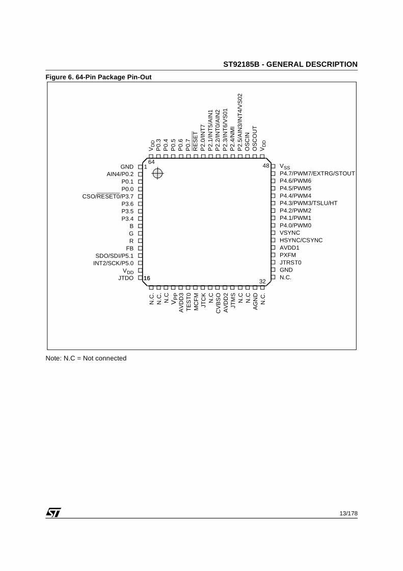
Figure 6. 64-Pin Package Pin-Out
Note: N.C = Not connected
GNDAIN4/P0.2
P0.1P0.0
CSO/RESET0/P3.7P3.6P3.5P3.4
BGR
FBSDO/SDI/P5.1
INT2/SCK/P5.0VDD
JTDO
VD
DP
0.3
P0.
4P
0.5
P0.
6P
0.7
RE
SE
TP
2.0/
INT
7P
2.1/
INT
5/A
IN1
P2.
2/IN
T0/
AIN
2P
2.3/
INT
6/V
S01
P2.
4/N
MI
P2.
5/A
IN3/
INT
4/V
S02
OS
CIN
OS
CO
UT
VD
D
VSSP4.7/PWM7/EXTRG/STOUTP4.6/PWM6P4.5/PWM5P4.4/PWM4P4.3/PWM3/TSLU/HTP4.2/PWM2P4.1/PWM1P4.0/PWM0VSYNCHSYNC/CSYNCAVDD1PXFMJTRST0GNDN.C.
N.C
.N
.C.
N.C
VP
PA
VD
D3
TE
ST
0M
CF
MJT
CK
N.C
CV
BS
OA
VD
D2
JTM
SN
.CN
.CA
GN
DN
.C.
164
16 32
48
16

14/178
ST92185B - GENERAL DESCRIPTION
PIN DESCRIPTION (Cont’d)
P0[7:0], P2[5:0], P3[7:4], P4[7:0], P5[1:0]I/O Port Lines (Input/Output, TTL or CMOS com-patible).
28 lines grouped into I/O ports, bit programmableas general purpose I/O or as Alternate functions(see I/O section).
Important: Note that open-drain outputs are forlogic levels only and are not true open drain.
1.2.1 I/O Port Alternate Functions. Each pin of the I/O ports of the ST92185B may as-sume software programmable Alternate Functions(see Table 1).
Table 1. ST92185B I/O Port Alternate Function Summary
Port
NameGeneral
Purpose I/OPin No.
Alternate FunctionsSDIP42 SDIP56
P0.0
All ports useable for general pur-pose I/O (input, output or bidi-rectional)
10 10 I/O
P0.1 9 9 I/O
P0.2 8 8 AIN4 I A/D Analog Data Input 4
P0.3 7 7 I/O
P0.4 6 6 I/O
P0.5 5 5 I/O
P0.6 4 4 I/O
P0.7 3 3 I/O
P2.0 1 1 INT7 I External Interrupt 7
P2.1 42 56AIN1 I A/D Analog Data Input 1
INT5 I External Interrupt 5
P2.2 41 55INT0 I External Interrupt 0
AIN2 I A/D Analog Data Input 2
P2.3 40 54INT6 I External Interrupt 6
VSO1 O Voltage Synthesis Output 1
P2.4 39 53 NMI I Non Maskable Interrupt Input
P2.5 38 52
AIN3 I A/D Analog Data Input 3
INT4 I External Interrupt 4
VSO2 O Voltage Synthesis Output 2
P3.4 14 14 I/O
P3.5 13 13 I/O
P3.6 12 12 I/O
P3.7 11 11RESET0 O Internal Reset Output
CSO O Composite Sync output
P4.0 28 42 PWM0 O PWM Output 0
P4.1 29 43 PWM1 O PWM Output 1
P4.2 30 44 PWM2 O PWM Output 2
P4.3 31 45
PWM3 O PWM Output 3
TSLU O Translucency Digital Output
HT O Half-tone Output
P4.4 32 46 PWM4 O PWM Output 4

15/178
ST92185B - GENERAL DESCRIPTION
P4.5
All ports useable for general pur-pose I/O (input, output or bidi-rectional)
33 47 PWM5 O PWM Output 5
P4.6 34 48 PWM6 O PWM Output 6
P4.7 35 49
EXTRG I A/D Converter External Trigger Input
PWM7 O PWM Output 7
STOUT O Standard Timer Output
P5.0 20 20INT2 I External Interrupt 2
SCK O SPI Serial Clock
P5.1 19 19SDO O SPI Serial Data Out
SDI I SPI Serial Data In
Port
NameGeneral
Purpose I/OPin No.
Alternate FunctionsSDIP42 SDIP56
16/178
ST92185B - GENERAL DESCRIPTION
PIN DESCRIPTION (Cont’d)
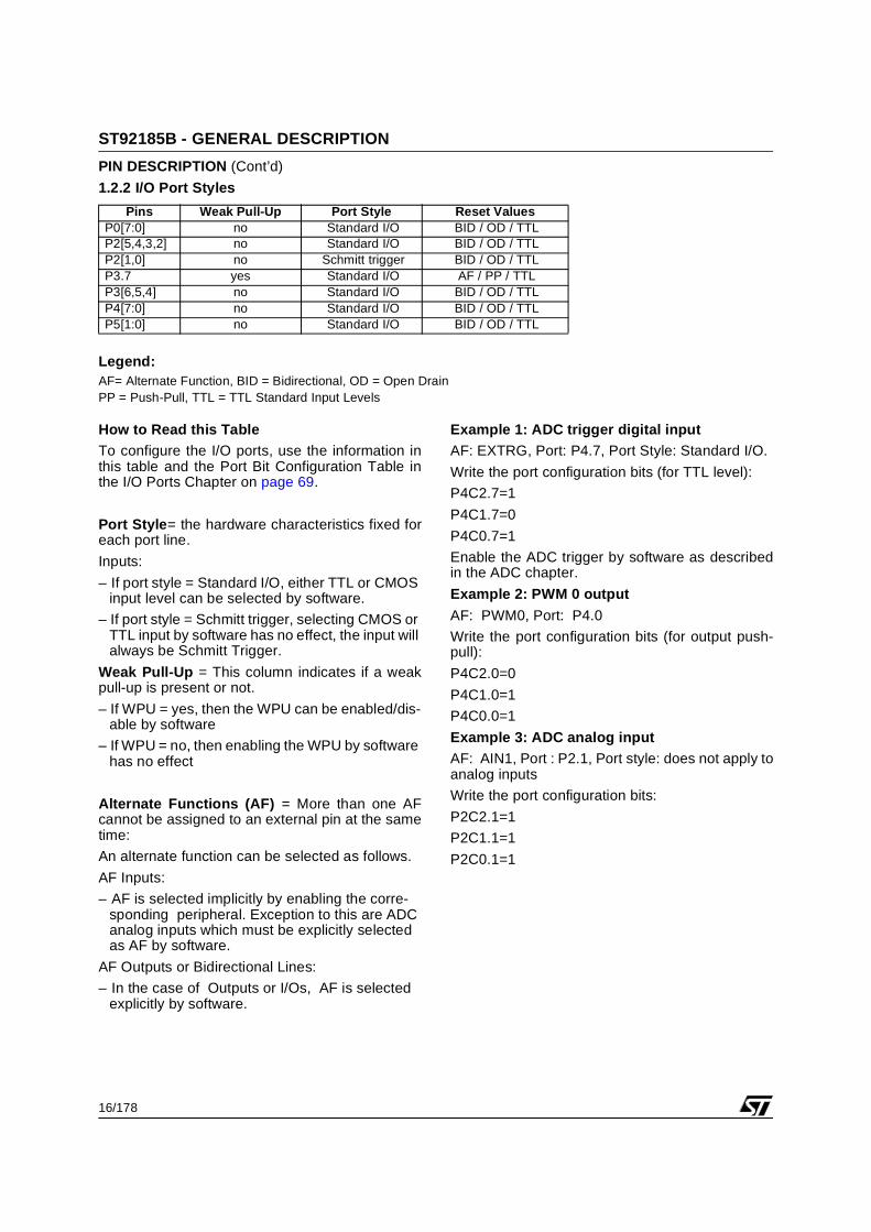
1.2.2 I/O Port Styles
Legend:AF= Alternate Function, BID = Bidirectional, OD = Open DrainPP = Push-Pull, TTL = TTL Standard Input Levels
How to Read this TableTo configure the I/O ports, use the information inthis table and the Port Bit Configuration Table inthe I/O Ports Chapter on page 69.
Port Style= the hardware characteristics fixed foreach port line.
Inputs:
– If port style = Standard I/O, either TTL or CMOS input level can be selected by software.
– If port style = Schmitt trigger, selecting CMOS or TTL input by software has no effect, the input will always be Schmitt Trigger.
Weak Pull-Up = This column indicates if a weakpull-up is present or not.
– If WPU = yes, then the WPU can be enabled/dis-able by software
– If WPU = no, then enabling the WPU by software has no effect
Alternate Functions (AF) = More than one AFcannot be assigned to an external pin at the sametime:
An alternate function can be selected as follows.
AF Inputs:
– AF is selected implicitly by enabling the corre-sponding peripheral. Exception to this are ADC analog inputs which must be explicitly selected as AF by software.
AF Outputs or Bidirectional Lines:
– In the case of Outputs or I/Os, AF is selected explicitly by software.
Example 1: ADC trigger digital inputAF: EXTRG, Port: P4.7, Port Style: Standard I/O.
Write the port configuration bits (for TTL level):
P4C2.7=1
P4C1.7=0
P4C0.7=1
Enable the ADC trigger by software as describedin the ADC chapter.
Example 2: PWM 0 output
AF: PWM0, Port: P4.0
Write the port configuration bits (for output push-pull):
P4C2.0=0
P4C1.0=1
P4C0.0=1
Example 3: ADC analog input AF: AIN1, Port : P2.1, Port style: does not apply toanalog inputs
Write the port configuration bits:
P2C2.1=1
P2C1.1=1
P2C0.1=1
Pins Weak Pull-Up Port Style Reset ValuesP0[7:0] no Standard I/O BID / OD / TTLP2[5,4,3,2] no Standard I/O BID / OD / TTLP2[1,0] no Schmitt trigger BID / OD / TTLP3.7 yes Standard I/O AF / PP / TTLP3[6,5,4] no Standard I/O BID / OD / TTLP4[7:0] no Standard I/O BID / OD / TTLP5[1:0] no Standard I/O BID / OD / TTL

17/178
ST92185B - GENERAL DESCRIPTION
1.3 MEMORY MAP
Internal ROMThe ROM memory is mapped in a single continu-ous area starting at address 0000h in MMU seg-ment 00h.
Internal RAM, 256 bytesThe internal RAM is mapped in MMU segment20h; from address FF00h to FFFFh.
Internal TDSRAMThe Internal TDSRAM is mapped starting at ad-dress 8000h in MMU segment 22h. It is a fully stat-ic memory.
Figure 7. ST92185B Memory Map
Device SizeStart
AddressEnd
Address
ST92185B1 16K 0000h 3FFFh
ST92185B2 24K 0000h 5FFFh
ST92185B3 32K 0000h 7FFFhDevice Size
StartAddress
End Address
ST92185B1/B2/B3 2K 8000h 87FFh
SEGMENT 064 Kbytes
00FFFFh
00C000h00BFFFh
008000h007FFFh
004000h
000000h
003FFFhPAGE 0 - 16 Kbytes
PAGE 1 - 16 Kbytes
PAGE 2 - 16 Kbytes
PAGE 3 - 16 Kbytes
SEGMENT 20h64 Kbytes
200000h
21FFFFh
20C000h20BFFFh
208000h207FFFh
204000h203FFFh
PAGE 80 - 16 Kbytes
PAGE 81 - 16 Kbytes
PAGE 82 - 16 Kbytes
PAGE 83 - 16 Kbytes
20FF00h
20FFFFh
RAM256 bytes
Internal
ReservedSEGMENT 21h64 Kbytes
20FFFFh
220000h
22FFFFh
210000h
SEGMENT 22h64 Kbytes
228000h
2287FFh2Kbytes
TDSRAM
Internal ROM
PAGE 88 - 16 Kbytes
PAGE 89 - 16 Kbytes
PAGE 90 - 16 Kbytes
PAGE 91 - 16 Kbytes22C000h22BFFFh
228000h227FFFh
224000h223FFFh
Reserved
Reserved
Reserved
Reserved
Reserved
Reserved
max. 64 Kbytes
32 Kbytes
Internal ROM
000000h
007FFFh
005FFFh
24K bytes Internal ROM16K bytes
24 Kbytes 003FFFh

18/178
ST92185B - GENERAL DESCRIPTION
1.4 REGISTER MAP
The following pages contain a list of ST92185Bregisters, grouped by peripheral or function.
Be very careful to correctly program both:
– The set of registers dedicated to a particularfunction or peripheral.
– Registers common to other functions.
In particular, double-check that any registers with“undefined” reset values have been correctly ini-tialised.
Warning: Note that in the EIVR and each IVR reg-ister, all bits are significant. Take care when defin-ing base vector addresses that entries in the Inter-rupt Vector table do not overlap.
Group F Pages Register Map
Register Page
0 2 3 11 21 32 33 35 38 39 55 59 62
R255 Res. Res.
Res.
Res.
Res.
OSD
TSU
Res
Res.
RCCU(PLL)
VS
Res.
R254SPI
Port 3TCC
R253 Res.
R252 WCR
MMU
TDSRAM
PWM
R251
WDT
Res.
Res
R250
Port 2
Res. Res.
R249
R248
R247
EXTINT
Res.
Res.
Res.R246
Port 5
MMU
R245
R244
R243 Res.
STIM
SYNCR242
Port 0 Port 4 A/DR241Res. Res.
R240

19/178
ST92185B - GENERAL DESCRIPTION
Table 2. Detailed Register Map
Group F Page Dec.
BlockReg. No.
RegisterName
DescriptionReset Value Hex.
Doc. Page
N/A
I/O
Port
0:5
R224 P0DR Port 0 Data Register FF
66
R226 P2DR Port 2 Data Register FF
R227 P3DR Port 3 Data Register FF
R228 P4DR Port 4 Data Register FF
R229 P5DR Port 5 Data Register FF
Core
R230 CICR Central Interrupt Control Register 87 53
R231 FLAGR Flag Register 00 26
R232 RP0 Pointer 0 Register xx 28
R233 RP1 Pointer 1 Register xx 28
R234 PPR Page Pointer Register xx 30
R235 MODER Mode Register E0 30
R236 USPHR User Stack Pointer High Register xx 33
R237 USPLR User Stack Pointer Low Register xx 33
R238 SSPHR System Stack Pointer High Reg. xx 33
R239 SSPLR System Stack Pointer Low Reg. xx 33
0
INT
R242 EITR External Interrupt Trigger Register 00 53
R243 EIPR External Interrupt Pending Reg. 00 54
R244 EIMR External Interrupt Mask-bit Reg. 00 54
R245 EIPLR External Interrupt Priority Level Reg. FF 54
R246 EIVR External Interrupt Vector Register x6 55
R247 NICR Nested Interrupt Control 00 55
WDT
R248 WDTHR Watchdog Timer High Register FF 78
R249 WDTLR Watchdog Timer Low Register FF 78
R250 WDTPR Watchdog Timer Prescaler Reg. FF 78
R251 WDTCR Watchdog Timer Control Register 12 78
R252 WCR Wait Control Register 7F 79
SPIR253 SPIDR SPI Data Register xx 150
R254 SPICR SPI Control Register 00 150
2
I/O
Port
0
R240 P0C0 Port 0 Configuration Register 0 00
66
R241 P0C1 Port 0 Configuration Register 1 00
R242 P0C2 Port 0 Configuration Register 2 00
I/O
Port
2
R248 P2C0 Port 2 Configuration Register 0 00
R249 P2C1 Port 2 Configuration Register 1 00
R250 P2C2 Port 2 Configuration Register 2 00
I/O
Port
3
R252 P3C0 Port 3 Configuration Register 0 00
R253 P3C1 Port 3 Configuration Register 1 00
R254 P3C2 Port 3 Configuration Register 2 00

20/178
ST92185B - GENERAL DESCRIPTION
3
I/O
Port
4
R240 P4C0 Port 4 Configuration Register 0 00
66
R241 P4C1 Port 4 Configuration Register 1 00
R242 P4C2 Port 4 Configuration Register 2 00
I/O
Port
5
R244 P5C0 Port 5 Configuration Register 0 00
R245 P5C1 Port 5 Configuration Register 1 00
R246 P5C2 Port 5 Configuration Register 2 00
11 STIM
R240 STH Counter High Byte Register FF 83
R241 STL Counter Low Byte Register FF 83
R242 STP Standard Timer Prescaler Register FF 83
R243 STC Standard Timer Control Register 14 83
21MMU
R240 DPR0 Data Page Register 0 xx 38
R241 DPR1 Data Page Register 1 xx 38
R242 DPR2 Data Page Register 2 xx 38
R243 DPR3 Data Page Register 3 xx 38
R244 CSR Code Segment Register 00 39
R248 ISR Interrupt Segment Register xx 39
R249 DMASR DMA Segment Register xx 39
Ext.Mem. R246 EMR2 External Memory Register 2 0F 56
32
OSD
R240 HBLANKR Horizontal Blank Register 03 121
R241 HPOSR Horizontal Position Register 03 121
R242 VPOSR Vertical Position Register 00 121
R243 FSCCR Full Screen Color Control Register 00 122
R244 HSCR Header & Status Control Register 2A 123
R245 NCSR National Character Set Control Register 00 124
R246 CHPOSR Cursor Horizontal Position Register 00 125
R247 CVPOSR Cursor Vertical Position Register 00 125
R248 SCLR Scrolling Control Low Register 00 126
R249 SCHR Scrolling Control High Register 00 127
R250 DCM0R Display Control Mode 0 Register 00 129
R251 DCM1R Display Control Mode 1 Register 00 130
R252 TDPR TDSRAM Pointer Register 00 130
R253 DE0R Display Enable 0 Control Register FF 131
R254 DE1R Display Enable 1 Control Register FF 131
R255 DE2R Display Enable 2 Control Register xF 131
33
R240 DCR Default Color Register 70 132
R241 CAPVR Cursor Absolute Vertical Position Register 00 132
R246 TDPPR TDSRAM Page Pointer Register x0 132
R247 TDHSPR TDSRAM Header/Status Pointer Register x0 132
35 SYNCR242 SCCS0R Sync Controller Control and Status Register 0 00 140
R243 SCCS1R Sync Controller Control and Status Register 1 00 141
38 TDSRAM R252 CONFIG TDSRAM Interface Configuration Register 02 87
Group F Page Dec.
BlockReg. No.
RegisterName
DescriptionReset Value Hex.
Doc. Page

21/178
ST92185B - GENERAL DESCRIPTION
Note: xx denotes a byte with an undefined value, however some of the bits may have defined values. Refer to registerdescription for details.
39 TCC
R251 PXCCR PLL Clock Control Register 00 66
R252 SLCCR Slicer Clock Control Register 00 66
R253 MCCR Main Clock Control Register 00 65
R254 SKCCR Skew Clock Control Register 00 65
55 RCCUR251 PCONF PLL Configuration Register 07 61
R254 SDRATH Clock Slow Down Unit Ratio Register2x,4xor 00
61
59
PWM
R240 CM0 Compare Register 0 00 163
R241 CM1 Compare Register 1 00 163
R242 CM2 Compare Register 2 00 163
R243 CM3 Compare Register 3 00 163
R244 CM4 Compare Register 4 00 163
R245 CM5 Compare Register 5 00 163
R246 CM6 Compare Register 6 00 163
R247 CM7 Compare Register 7 00 163
R248 ACR Autoclear Register FF 164
R249 CCR Counter Register 00 164
R250 PCTL Prescaler and Control Register 0C 164
R251 OCPL Output Complement Register 00 165
R252 OER Output Enable Register 00 165
VSR254 VSDR1 Data and Control Register 1 00 160
R255 VSDR2 Data Register 2 00 160
62 ADC
R240 ADDTR Channel i Data Register xx 155
R241 ADCLR Control Logic Register 00 154
R242 ADINT AD Interrupt Register 01 155
Group F Page Dec.
BlockReg. No.
RegisterName
DescriptionReset Value Hex.
Doc. Page

22/178
ST92185B - DEVICE ARCHITECTURE
2 DEVICE ARCHITECTURE
2.1 CORE ARCHITECTURE
The ST9 Core or Central Processing Unit (CPU)features a highly optimised instruction set, capableof handling bit, byte (8-bit) and word (16-bit) data,as well as BCD and Boolean formats; 14 address-ing modes are available.
Four independent buses are controlled by theCore: a 16-bit Memory bus, an 8-bit Register databus, an 8-bit Register address bus and a 6-bit In-terrupt/DMA bus which connects the interrupt andDMA controllers in the on-chip peripherals with theCore.
This multiple bus architecture affords a high de-gree of pipelining and parallel operation, thus mak-ing the ST9 family devices highly efficient, both fornumerical calculation, data handling and with re-gard to communication with on-chip peripheral re-sources.
2.2 MEMORY SPACES
There are two separate memory spaces:
– The Register File, which comprises 240 8-bitregisters, arranged as 15 groups (Group 0 to E),each containing sixteen 8-bit registers plus up to64 pages of 16 registers mapped in Group F,
which hold data and control bits for the on-chipperipherals and I/Os.
– A single linear memory space accommodatingboth program and data. All of the physically sep-arate memory areas, including the internal ROM,internal RAM and external memory are mappedin this common address space. The total ad-dressable memory space of 4 Mbytes (limited bythe size of on-chip memory and the number ofexternal address pins) is arranged as 64 seg-ments of 64 Kbytes. Each segment is furthersubdivided into four pages of 16 Kbytes, as illus-trated in Figure 1. A Memory Management Unituses a set of pointer registers to address a 22-bitmemory field using 16-bit address-based instruc-tions.
2.2.1 Register FileThe Register File consists of (see Figure 2):
– 224 general purpose registers (Group 0 to D,registers R0 to R223)
– 6 system registers in the System Group (GroupE, registers R224 to R239)
– Up to 64 pages, depending on device configura-tion, each containing up to 16 registers, mappedto Group F (R240 to R255), see Figure 3.
Figure 8. Single Program and Data Memory Address Space
3FFFFFh
3F0000h3EFFFFh
3E0000h
20FFFFh
02FFFFh
020000h
01FFFFh
010000h
00FFFFh
000000h
876543210
63
62
2
1
0
Address 16K Pages 64K Segments
up to 4 Mbytes
Data Code
255254253252251250249248247
91011
21FFFFh
210000h133134135
33Reserved132

23/178
ST92185B - DEVICE ARCHITECTURE
MEMORY SPACES (Cont’d)
Figure 9. Register Groups Figure 10. Page Pointer for Group F mapping
Figure 11. Addressing the Register File
F
E
D
C
B
A
9
8
7
6
5
4
3
PAGED REGISTERS
SYSTEM REGISTERS
2
1
00 0
15
255240239224223
VA00432
UP TO64 PAGES
GENERAL
REGISTERSPURPOSE
224
PAGE 63
PAGE 5
PAGE 0
PAGE POINTER
R255
R240
R224
R0 VA00433
R234
REGISTER FILE
SYSTEM REGISTERS
GROUP D
GROUP B
GROUP C
(1100) (0011)
R192
R207
255240239224223
F
E
D
C
B
A
9
8
7
6
5
4
3
2
1
0 15
VR0001180 0
R195
R195(R0C3h)
PAGED REGISTERS

24/178
ST92185B - DEVICE ARCHITECTURE
MEMORY SPACES (Cont’d)
2.2.2 Register Addressing
Register File registers, including Group F pagedregisters (but excluding Group D), may be ad-dressed explicitly by means of a decimal, hexa-decimal or binary address; thus R231, RE7h andR11100111b represent the same register (seeFigure 4). Group D registers can only be ad-dressed in Working Register mode.
Note that an upper case “R” is used to denote thisdirect addressing mode.
Working Registers
Certain types of instruction require that registersbe specified in the form “rx”, where x is in therange 0 to 15: these are known as Working Regis-ters.
Note that a lower case “r” is used to denote this in-direct addressing mode.
Two addressing schemes are available: a singlegroup of 16 working registers, or two separatelymapped groups, each consisting of 8 working reg-isters. These groups may be mapped starting atany 8 or 16 byte boundary in the register file bymeans of dedicated pointer registers. This tech-nique is described in more detail in Section 1.3.3,and illustrated in Figure 5 and in Figure 6.
System RegistersThe 16 registers in Group E (R224 to R239) areSystem registers and may be addressed using anyof the register addressing modes. These registersare described in greater detail in Section 1.3.
Paged Registers
Up to 64 pages, each containing 16 registers, maybe mapped to Group F. These are addressed us-ing any register addressing mode, in conjunctionwith the Page Pointer register, R234, which is oneof the System registers. This register selects thepage to be mapped to Group F and, once set,does not need to be changed if two or more regis-ters on the same page are to be addressed in suc-cession.
Therefore if the Page Pointer, R234, is set to 5, theinstructions:
spp #5ld R242, r4
will load the contents of working register r4 into thethird register of page 5 (R242).
These paged registers hold data and control infor-mation relating to the on-chip peripherals, eachperipheral always being associated with the samepages and registers to ensure code compatibilitybetween ST9 devices. The number of these regis-ters therefore depends on the peripherals whichare present in the specific ST9 family device. Inother words, pages only exist if the relevant pe-ripheral is present.
Table 3. Register File Organization
Hex.Address
DecimalAddress
FunctionRegister
File Group
F0-FF 240-255Paged
RegistersGroup F
E0-EF 224-239System
RegistersGroup E
D0-DF 208-223
GeneralPurposeRegisters
Group D
C0-CF 192-207 Group C
B0-BF 176-191 Group B
A0-AF 160-175 Group A
90-9F 144-159 Group 9
80-8F 128-143 Group 8
70-7F 112-127 Group 7
60-6F 96-111 Group 6
50-5F 80-95 Group 5
40-4F 64-79 Group 4
30-3F 48-63 Group 3
20-2F 32-47 Group 2
10-1F 16-31 Group 1
00-0F 00-15 Group 0

25/178
ST92185B - DEVICE ARCHITECTURE
2.3 SYSTEM REGISTERS
The System registers are listed in Table 2 SystemRegisters (Group E). They are used to perform allthe important system settings. Their purpose is de-scribed in the following pages. Refer to the chapterdealing with I/O for a description of the PORT[5:0]Data registers.
Table 4. System Registers (Group E)
2.3.1 Central Interrupt Control RegisterPlease refer to the ”INTERRUPT” chapter for a de-tailed description of the ST9 interrupt philosophy.
CENTRAL INTERRUPT CONTROL REGISTER(CICR)R230 - Read/WriteRegister Group: E (System)Reset Value: 1000 0111 (87h)
Bit 7 = GCEN: Global Counter Enable. This bit is the Global Counter Enable of the Multi-function Timers. The GCEN bit is ANDed with theCE bit in the TCR Register (only in devices featur-ing the MFT Multifunction Timer) in order to enablethe Timers when both bits are set. This bit is set af-ter the Reset cycle.
Note: If an MFT is not included in the ST9 device,then this bit has no effect.
Bit 6 = TLIP: Top Level Interrupt Pending.This bit is set by hardware when a Top Level Inter-rupt Request is recognized. This bit can also beset by software to simulate a Top Level InterruptRequest.0: No Top Level Interrupt pending1: Top Level Interrupt pending
Bit 5 = TLI: Top Level Interrupt bit. 0: Top Level Interrupt is acknowledged depending
on the TLNM bit in the NICR Register.1: Top Level Interrupt is acknowledged depending
on the IEN and TLNM bits in the NICR Register (described in the Interrupt chapter).
Bit 4 = IEN: Interrupt Enable .This bit is cleared by interrupt acknowledgement,and set by interrupt return (iret). IEN is modifiedimplicitly by iret, ei and di instructions or by aninterrupt acknowledge cycle. It can also be explic-itly written by the user, but only when no interruptis pending. Therefore, the user should execute adi instruction (or guarantee by other means thatno interrupt request can arrive) before any writeoperation to the CICR register.0: Disable all interrupts except Top Level Interrupt. 1: Enable Interrupts
Bit 3 = IAM: Interrupt Arbitration Mode. This bit is set and cleared by software to select thearbitration mode.0: Concurrent Mode 1: Nested Mode.
Bits 2:0 = CPL[2:0]: Current Priority Level.These three bits record the priority level of the rou-tine currently running (i.e. the Current Priority Lev-el, CPL). The highest priority level is representedby 000, and the lowest by 111. The CPL bits canbe set by hardware or software and provide thereference according to which subsequent inter-rupts are either left pending or are allowed to inter-rupt the current interrupt service routine. When thecurrent interrupt is replaced by one of a higher pri-ority, the current priority value is automaticallystored until required in the NICR register.
R239 (EFh) SSPLR
R238 (EEh) SSPHR
R237 (EDh) USPLR
R236 (ECh) USPHR
R235 (EBh) MODE REGISTER
R234 (EAh) PAGE POINTER REGISTER
R233 (E9h) REGISTER POINTER 1
R232 (E8h) REGISTER POINTER 0
R231 (E7h) FLAG REGISTER
R230 (E6h) CENTRAL INT. CNTL REG
R229 (E5h) PORT5 DATA REG.
R228 (E4h) PORT4 DATA REG.
R227 (E3h) PORT3 DATA REG.
R226 (E2h) PORT2 DATA REG.
R225 (E1h) PORT1 DATA REG.
R224 (E0h) PORT0 DATA REG.
7 0
GCEN TLIP TLI IEN IAM CPL2 CPL1 CPL0

26/178
ST92185B - DEVICE ARCHITECTURE
SYSTEM REGISTERS (Cont’d)
2.3.2 Flag Register
The Flag Register contains 8 flags which indicatethe CPU status. During an interrupt, the flag regis-ter is automatically stored in the system stack areaand recalled at the end of the interrupt service rou-tine, thus returning the CPU to its original status.
This occurs for all interrupts and, when operatingin nested mode, up to seven versions of the flagregister may be stored.
FLAG REGISTER (FLAGR)R231- Read/WriteRegister Group: E (System) Reset value: 0000 0000 (00h)
Bit 7 = C: Carry Flag. The carry flag is affected by:
Addition (add, addw, adc, adcw),Subtraction (sub, subw, sbc, sbcw),Compare (cp, cpw),Shift Right Arithmetic (sra, sraw),Shift Left Arithmetic (sla, slaw),Swap Nibbles (swap),Rotate (rrc, rrcw, rlc, rlcw, ror,rol),Decimal Adjust (da),Multiply and Divide (mul, div, divws).
When set, it generally indicates a carry out of themost significant bit position of the register beingused as an accumulator (bit 7 for byte operationsand bit 15 for word operations).
The carry flag can be set by the Set Carry Flag(scf) instruction, cleared by the Reset Carry Flag(rcf) instruction, and complemented by the Com-plement Carry Flag (ccf) instruction.
Bit 6 = Z: Zero Flag. The Zero flag is affected by:Addition (add, addw, adc, adcw),Subtraction (sub, subw, sbc, sbcw),Compare (cp, cpw),Shift Right Arithmetic (sra, sraw),Shift Left Arithmetic (sla, slaw),Swap Nibbles (swap),Rotate (rrc, rrcw, rlc, rlcw, ror,rol),Decimal Adjust (da),Multiply and Divide (mul, div, divws),Logical (and, andw, or, orw, xor,xorw, cpl),Increment and Decrement (inc, incw, dec,
decw),Test (tm, tmw, tcm, tcmw, btset).
In most cases, the Zero flag is set when the contentsof the register being used as an accumulator be-come zero, following one of the above operations.
Bit 5 = S: Sign Flag.The Sign flag is affected by the same instructionsas the Zero flag.
The Sign flag is set when bit 7 (for a byte opera-tion) or bit 15 (for a word operation) of the registerused as an accumulator is one.
Bit 4 = V: Overflow Flag.The Overflow flag is affected by the same instruc-tions as the Zero and Sign flags.
When set, the Overflow flag indicates that a two's-complement number, in a result register, is in er-ror, since it has exceeded the largest (or is lessthan the smallest), number that can be represent-ed in two’s-complement notation.
Bit 3 = DA: Decimal Adjust Flag. The DA flag is used for BCD arithmetic. Since thealgorithm for correcting BCD operations is differ-ent for addition and subtraction, this flag is used tospecify which type of instruction was executedlast, so that the subsequent Decimal Adjust (da)operation can perform its function correctly. TheDA flag cannot normally be used as a test condi-tion by the programmer.
Bit 2 = H: Half Carry Flag. The H flag indicates a carry out of (or a borrow in-to) bit 3, as the result of adding or subtracting two8-bit bytes, each representing two BCD digits. TheH flag is used by the Decimal Adjust (da) instruc-tion to convert the binary result of a previous addi-tion or subtraction into the correct BCD result. Likethe DA flag, this flag is not normally accessed bythe user.
Bit 1 = Reserved bit (must be 0).
Bit 0 = DP: Data/Program Memory Flag. This bit indicates the memory area addressed. Itsvalue is affected by the Set Data Memory (sdm)and Set Program Memory (spm) instructions. Re-fer to the Memory Management Unit for further de-tails.
7 0
C Z S V DA H - DP

27/178
ST92185B - DEVICE ARCHITECTURE
SYSTEM REGISTERS (Cont’d)
If the bit is set, data is accessed using the DataPointers (DPRs registers), otherwise it is pointedto by the Code Pointer (CSR register); therefore,the user initialization routine must include a Sdminstruction. Note that code is always pointed to bythe Code Pointer (CSR).
Note: In the current ST9 devices, the DP flag isonly for compatibility with software developed forthe first generation of ST9 devices. With the singlememory addressing space, its use is now redun-dant. It must be kept to 1 with a Sdm instruction atthe beginning of the program to ensure a normaluse of the different memory pointers.
2.3.3 Register Pointing Techniques
Two registers within the System register group,are used as pointers to the working registers. Reg-ister Pointer 0 (R232) may be used on its own as asingle pointer to a 16-register working space, or inconjunction with Register Pointer 1 (R233), topoint to two separate 8-register spaces.
For the purpose of register pointing, the 16 registergroups of the register file are subdivided into 32 8-register blocks. The values specified with the SetRegister Pointer instructions refer to the blocks tobe pointed to in twin 8-register mode, or to the low-er 8-register block location in single 16-registermode.
The Set Register Pointer instructions srp, srp0and srp1 automatically inform the CPU whetherthe Register File is to operate in single 16-registermode or in twin 8-register mode. The srp instruc-tion selects the single 16-register group mode and
specifies the location of the lower 8-register block,while the srp0 and srp1 instructions automatical-ly select the twin 8-register group mode and spec-ify the locations of each 8-register block.
There is no limitation on the order or position ofthese register groups, other than that they muststart on an 8-register boundary in twin 8-registermode, or on a 16-register boundary in single 16-register mode.
The block number should always be an evennumber in single 16-register mode. The 16-regis-ter group will always start at the block whosenumber is the nearest even number equal to orlower than the block number specified in the srpinstruction. Avoid using odd block numbers, sincethis can be confusing if twin mode is subsequentlyselected.
Thus:
srp #3 will be interpreted as srp #2 and will al-low using R16 ..R31 as r0 .. r15.
In single 16-register mode, the working registersare referred to as r0 to r15. In twin 8-registermode, registers r0 to r7 are in the block pointedto by RP0 (by means of the srp0 instruction),while registers r8 to r15 are in the block pointedto by RP1 (by means of the srp1 instruction).
Caution: Group D registers can only be accessedas working registers using the Register Pointers,or by means of the Stack Pointers. They cannot beaddressed explicitly in the form “Rxxx”.

28/178
ST92185B - DEVICE ARCHITECTURE
SYSTEM REGISTERS (Cont’d)
POINTER 0 REGISTER (RP0) R232 - Read/WriteRegister Group: E (System)Reset Value: xxxx xx00 (xxh)
Bits 7:3 = RG[4:0]: Register Group number.These bits contain the number (in the range 0 to31) of the register block specified in the srp0 orsrp instructions. In single 16-register mode thenumber indicates the lower of the two 8-registerblocks to which the 16 working registers are to bemapped, while in twin 8-register mode it indicatesthe 8-register block to which r0 to r7 are to bemapped.
Bit 2 = RPS: Register Pointer Selector. This bit is set by the instructions srp0 and srp1 toindicate that the twin register pointing mode is se-lected. The bit is reset by the srp instruction to in-dicate that the single register pointing mode is se-lected.0: Single register pointing mode1: Twin register pointing mode
Bits 1:0: Reserved. Forced by hardware to zero.
POINTER 1 REGISTER (RP1) R233 - Read/WriteRegister Group: E (System)Reset Value: xxxx xx00 (xxh)
This register is only used in the twin register point-ing mode. When using the single register pointingmode, or when using only one of the twin registergroups, the RP1 register must be considered asRESERVED and may NOT be used as a generalpurpose register.
Bits 7:3 = RG[4:0]: Register Group number.These bits contain the number (in the range 0 to31) of the 8-register block specified in the srp1 in-struction, to which r8 to r15 are to be mapped.
Bit 2 = RPS: Register Pointer Selector.This bit is set by the srp0 and srp1 instructions toindicate that the twin register pointing mode is se-lected. The bit is reset by the srp instruction to in-dicate that the single register pointing mode is se-lected.0: Single register pointing mode1: Twin register pointing mode
Bits 1:0: Reserved. Forced by hardware to zero.
7 0
RG4 RG3 RG2 RG1 RG0 RPS 0 0
7 0
RG4 RG3 RG2 RG1 RG0 RPS 0 0

29/178
ST92185B - DEVICE ARCHITECTURE
SYSTEM REGISTERS (Cont’d)
Figure 12. Pointing to a single group of 16registers
Figure 13. Pointing to two groups of 8 registers
31
30
29
28
27
26
25
9
8
7
6
5
4
3
2
1
0
F
E
D
4
3
2
1
0
BLOCKNUMBER
REGISTERGROUP
REGISTERFILE
REGISTERPOINTER 0
srp #2set by:
instruction
points to:
GROUP 1
addressed byBLOCK 2
r15
r0
31
30
29
28
27
26
25
9
8
7
6
5
4
3
2
1
0
F
E
D
4
3
2
1
0
BLOCKNUMBER
REGISTERGROUP
REGISTERFILE
REGISTERPOINTER 0
srp0 #2
set by:
instructions
point to:
GROUP 1addressed by
BLOCK 2
®ISTERPOINTER 1
srp1 #7&
GROUP 3
addressed byBLOCK 7
r7
r0
r15
r8

30/178
ST92185B - DEVICE ARCHITECTURE
SYSTEM REGISTERS (Cont’d)
2.3.4 Paged Registers
Up to 64 pages, each containing 16 registers, maybe mapped to Group F. These paged registershold data and control information relating to theon-chip peripherals, each peripheral always beingassociated with the same pages and registers toensure code compatibility between ST9 devices.The number of these registers depends on the pe-ripherals present in the specific ST9 device. In oth-er words, pages only exist if the relevant peripher-al is present.
The paged registers are addressed using the nor-mal register addressing modes, in conjunction withthe Page Pointer register, R234, which is one ofthe System registers. This register selects thepage to be mapped to Group F and, once set,does not need to be changed if two or more regis-ters on the same page are to be addressed in suc-cession.Thus the instructions:spp #5ld R242, r4
will load the contents of working register r4 into thethird register of page 5 (R242).
Warning: During an interrupt, the PPR register isnot saved automatically in the stack. If needed, itshould be saved/restored by the user within the in-terrupt routine.
PAGE POINTER REGISTER (PPR)R234 - Read/WriteRegister Group: E (System)Reset value: xxxx xx00 (xxh)
Bits 7:2 = PP[5:0]: Page Pointer.These bits contain the number (in the range 0 to63) of the page specified in the spp instruction.Once the page pointer has been set, there is no
need to refresh it unless a different page is re-quired.
Bits 1:0: Reserved. Forced by hardware to 0.
2.3.5 Mode Register
The Mode Register allows control of the followingoperating parameters:
– Selection of internal or external System and UserStack areas,
– Management of the clock frequency,
– Enabling of Bus request and Wait signals wheninterfacing to external memory.
MODE REGISTER (MODER)R235 - Read/WriteRegister Group: E (System)Reset value: 1110 0000 (E0h)
Bit 7 = SSP: System Stack Pointer. This bit selects an internal or external SystemStack area.0: External system stack area, in memory space.1: Internal system stack area, in the Register File
(reset state).
Bit 6 = USP: User Stack Pointer. This bit selects an internal or external User Stackarea.0: External user stack area, in memory space.1: Internal user stack area, in the Register File (re-
set state).
Bit 5 = DIV2: Crystal Oscillator Clock Divided by 2. This bit controls the divide-by-2 circuit operatingon the crystal oscillator clock (CLOCK1). 0: Clock divided by 11: Clock divided by 2
7 0
PP5 PP4 PP3 PP2 PP1 PP0 0 0
7 0
SSP USP DIV2 PRS2 PRS1 PRS0 BRQEN HIMP

31/178
ST92185B - DEVICE ARCHITECTURE
Bits 4:2 = PRS[2:0]: CPUCLK Prescaler.These bits load the prescaler division factor for theinternal clock (INTCLK). The prescaler factor se-lects the internal clock frequency, which can be di-vided by a factor from 1 to 8. Refer to the Resetand Clock Control chapter for further information.
Bit 1 = BRQEN: Bus Request Enable. 0: External Memory Bus Request disabled1: External Memory Bus Request enabled on
BREQ pin (where available).
Note: Disregard this bit if BREQ pin is not availa-ble.
Bit 0 = HIMP: High Impedance Enable.When any of Ports 0, 1, 2 or 6 depending on de-vice configuration, are programmed as Addressand Data lines to interface external Memory, theselines and the Memory interface control lines (AS,DS, R/W) can be forced into the High Impedance

32/178
ST92185B - DEVICE ARCHITECTURE
SYSTEM REGISTERS (Cont’d)
state by setting the HIMP bit. When this bit is reset,it has no effect.
Setting the HIMP bit is recommended for noise re-duction when only internal Memory is used.
If Port 1 and/or 2 are declared as an address ANDas an I/O port (for example: P10... P14 = Address,and P15... P17 = I/O), the HIMP bit has no effecton the I/O lines.
2.3.6 Stack PointersTwo separate, double-register stack pointers areavailable: the System Stack Pointer and the UserStack Pointer, both of which can address registersor memory.
The stack pointers point to the “bottom” of thestacks which are filled using the push commandsand emptied using the pop commands. The stackpointer is automatically pre-decremented whendata is “pushed” in and post-incremented whendata is “popped” out.
The push and pop commands used to manage theSystem Stack may be addressed to the UserStack by adding the suffix “u” . To use a stack in-struction for a word, the suffix “w” is added. Thesesuffixes may be combined.
When bytes (or words) are “popped” out from astack, the contents of the stack locations are un-changed until fresh data is loaded. Thus, whendata is “popped” from a stack area, the stack con-tents remain unchanged.
Note: Instructions such as: pushuw RR236 orpushw RR238, as well as the correspondingpop instructions (where R236 & R237, and R238& R239 are themselves the user and system stackpointers respectively), must not be used, since thepointer values are themselves automaticallychanged by the push or pop instruction, thus cor-rupting their value.
System StackThe System Stack is used for the temporary stor-age of system and/or control data, such as theFlag register and the Program counter.
The following automatically push data onto theSystem Stack:
– InterruptsWhen entering an interrupt, the PC and the FlagRegister are pushed onto the System Stack. If theENCSR bit in the EMR2 register is set, then the
Code Segment Register is also pushed onto theSystem Stack.
– Subroutine CallsWhen a call instruction is executed, only the PCis pushed onto stack, whereas when a calls in-struction (call segment) is executed, both the PCand the Code Segment Register are pushed ontothe System Stack.
– Link Instruction
The link or linku instructions create a C lan-guage stack frame of user-defined length in theSystem or User Stack.
All of the above conditions are associated withtheir counterparts, such as return instructions,which pop the stored data items off the stack.
User Stack
The User Stack provides a totally user-controlledstacking area.
The User Stack Pointer consists of two registers,R236 and R237, which are both used for address-ing a stack in memory. When stacking in the Reg-ister File, the User Stack Pointer High Register,R236, becomes redundant but must be consid-ered as reserved.
Stack Pointers
Both System and User stacks are pointed to bydouble-byte stack pointers. Stacks may be set upin RAM or in the Register File. Only the lower bytewill be required if the stack is in the Register File.The upper byte must then be considered as re-served and must not be used as a general purposeregister.
The stack pointer registers are located in the Sys-tem Group of the Register File, this is illustrated inTable 2 System Registers (Group E).
Stack Location
Care is necessary when managing stacks as thereis no limit to stack sizes apart from the bottom ofany address space in which the stack is placed.Consequently programmers are advised to use astack pointer value as high as possible, particular-ly when using the Register File as a stacking area.
Group D is a good location for a stack in the Reg-ister File, since it is the highest available area. Thestacks may be located anywhere in the first 14groups of the Register File (internal stacks) or inRAM (external stacks).
Note. Stacks must not be located in the PagedRegister Group or in the System Register Group.

33/178
ST92185B - DEVICE ARCHITECTURE
SYSTEM REGISTERS (Cont’d)
USER STACK POINTER HIGH REGISTER (USPHR)R236 - Read/WriteRegister Group: E (System)Reset value: undefined
USER STACK POINTER LOW REGISTER (USPLR)R237 - Read/WriteRegister Group: E (System)Reset value: undefined
Figure 14. Internal Stack Mode
SYSTEM STACK POINTER HIGH REGISTER(SSPHR)R238 - Read/WriteRegister Group: E (System)Reset value: undefined
SYSTEM STACK POINTER LOW REGISTER(SSPLR)R239 - Read/WriteRegister Group: E (System)Reset value: undefined
Figure 15. External Stack Mode
7 0
USP15 USP14 USP13 USP12 USP11 USP10 USP9 USP8
7 0
USP7 USP6 USP5 USP4 USP3 USP2 USP1 USP0
F
E
D
4
3
2
1
0
REGISTERFILE
STACK POINTER (LOW)
points to:
STACK
7 0
SSP15 SSP14 SSP13 SSP12 SSP11 SSP10 SSP9 SSP8
7 0
SSP7 SSP6 SSP5 SSP4 SSP3 SSP2 SSP1 SSP0
F
E
D
4
3
2
1
0
REGISTERFILE
STACK POINTER (LOW)
point to:
STACK
MEMORY
STACK POINTER (HIGH)
&

34/178
ST92185B - DEVICE ARCHITECTURE
2.4 MEMORY ORGANIZATION
Code and data are accessed within the same line-ar address space. All of the physically separatememory areas, including the internal ROM, inter-nal RAM and external memory are mapped in acommon address space.
The ST9 provides a total addressable memoryspace of 4 Mbytes. This address space is ar-ranged as 64 segments of 64 Kbytes; each seg-ment is again subdivided into four 16 Kbyte pages.
The mapping of the various memory areas (inter-nal RAM or ROM, external memory) differs fromdevice to device. Each 64-Kbyte physical memorysegment is mapped either internally or externally;if the memory is internal and smaller than 64Kbytes, the remaining locations in the 64-Kbytesegment are not used (reserved).
Refer to the Register and Memory Map Chapterfor more details on the memory map.

35/178
ST92185B - DEVICE ARCHITECTURE
2.5 MEMORY MANAGEMENT UNIT
The CPU Core includes a Memory ManagementUnit (MMU) which must be programmed to per-form memory accesses (even if external memoryis not used).
The MMU is controlled by 7 registers and 2 bits(ENCSR and DPRREM) present in EMR2, whichmay be written and read by the user program.These registers are mapped within group F, Page21 of the Register File. The 7 registers may be
sub-divided into 2 main groups: a first group of four8-bit registers (DPR[3:0]), and a second group ofthree 6-bit registers (CSR, ISR, and DMASR). Thefirst group is used to extend the address duringData Memory access (DPR[3:0]). The second isused to manage Program and Data Memory ac-cesses during Code execution (CSR), InterruptsService Routines (ISR or CSR), and DMA trans-fers (DMASR or ISR).
Figure 16. Page 21 Registers
DMASR
ISR
EMR2
EMR1
CSR
DPR3
DPR2
DPR1
DPR0
R255
R254
R253
R252
R251
R250
R249
R248
R247
R246
R245
R244
R243
R242
R241
R240
FFh
FEh
FDh
FCh
FBh
FAh
F9h
F8h
F7h
F6h
F5h
F4h
F3h
F2h
F1h
F0h
MMU
EM
Page 21
MMU
MMU
Bit DPRREM=0
SSPLRSSPHRUSPLRUSPHRMODER
PPRRP1RP0
FLAGRCICRP5DRP4DRP3DRP2DRP1DRP0DR
DMASRISR
EMR2EMR1CSRDPR3DPR2
1DPR0
Bit DPRREM=1
SSPLRSSPHRUSPLRUSPHRMODER
PPRRP1RP0
FLAGRCICRP5DRP4DR
P3DRP2DRP1DRP0DR
DMASRISR
EMR2EMR1CSR
DPR3DPR2DPR1DPR0
Relocation of P[3:0] and DPR[3:0] Registers
(default setting)

36/178
ST92185B - DEVICE ARCHITECTURE
2.6 ADDRESS SPACE EXTENSION
To manage 4 Mbytes of addressing space, it isnecessary to have 22 address bits. The MMUadds 6 bits to the usual 16-bit address, thus trans-lating a 16-bit virtual address into a 22-bit physicaladdress. There are 2 different ways to do this de-pending on the memory involved and on the oper-ation being performed.
2.6.1 Addressing 16-Kbyte PagesThis extension mode is implicitly used to addressData memory space if no DMA is being performed.
The Data memory space is divided into 4 pages of16 Kbytes. Each one of the four 8-bit registers(DPR[3:0], Data Page Registers) selects a differ-ent 16-Kbyte page. The DPR registers allow ac-cess to the entire memory space which contains256 pages of 16 Kbytes.
Data paging is performed by extending the 14 LSBof the 16-bit address with the contents of a DPRregister. The two MSBs of the 16-bit address areinterpreted as the identification number of the DPRregister to be used. Therefore, the DPR registers
are involved in the following virtual address rang-es:
DPR0: from 0000h to 3FFFh;
DPR1: from 4000h to 7FFFh;
DPR2: from 8000h to BFFFh;
DPR3: from C000h to FFFFh.
The contents of the selected DPR register specifyone of the 256 possible data memory pages. This8-bit data page number, in addition to the remain-ing 14-bit page offset address forms the physical22-bit address (see Figure 10).
A DPR register cannot be modified via an address-ing mode that uses the same DPR register. For in-stance, the instruction “POPW DPR0” is legal onlyif the stack is kept either in the register file or in amemory location above 8000h, where DPR2 andDPR3 are used. Otherwise, since DPR0 andDPR1 are modified by the instruction, unpredicta-ble behaviour could result.
Figure 17. Addressing via DPR[3:0]
DPR0 DPR1 DPR2 DPR3
00 01 10 11
16-bit virtual address
22-bit physical address
8 bits
MMU registers
2 MSB
14 LSB

37/178
ST92185B - DEVICE ARCHITECTURE
ADDRESS SPACE EXTENSION (Cont’d)
2.6.2 Addressing 64-Kbyte Segments
This extension mode is used to address Datamemory space during a DMA and Program mem-ory space during any code execution (normal codeand interrupt routines).
Three registers are used: CSR, ISR, and DMASR.The 6-bit contents of one of the registers CSR,ISR, or DMASR define one out of 64 Memory seg-ments of 64 Kbytes within the 4 Mbytes addressspace. The register contents represent the 6MSBs of the memory address, whereas the 16LSBs of the address (intra-segment address) aregiven by the virtual 16-bit address (see Figure 11).
2.7 MMU REGISTERS
The MMU uses 7 registers mapped into Group F,Page 21 of the Register File and 2 bits of theEMR2 register.
Most of these registers do not have a default valueafter reset.
2.7.1 DPR[3:0]: Data Page Registers
The DPR[3:0] registers allow access to the entire 4Mbyte memory space composed of 256 pages of16 Kbytes.
2.7.1.1 Data Page Register Relocation
If these registers are to be used frequently, theymay be relocated in register group E, by program-ming bit 5 of the EMR2-R246 register in page 21. Ifthis bit is set, the DPR[3:0] registers are located atR224-227 in place of the Port 0-3 Data Registers,which are re-mapped to the default DPR's loca-tions: R240-243 page 21.
Data Page Register relocation is illustrated in Fig-ure 9.
Figure 18. Addressing via CSR, ISR, and DMASR
Fetching program
Data Memory
Fetching interrupt
instruction
accessed in DMA
instruction or DMA access to Program Memory
16-bit virtual address
22-bit physical address
6 bits
MMU registers
CSR ISRDMASR
1 2 3
1
2
3

38/178
ST92185B - DEVICE ARCHITECTURE
MMU REGISTERS (Cont’d)
DATA PAGE REGISTER 0 (DPR0)R240 - Read/WriteRegister Page: 21Reset value: undefined
This register is relocated to R224 if EMR2.5 is set.
Bits 7:0 = DPR0_[7:0]: These bits define the 16-Kbyte Data Memory page number. They are usedas the most significant address bits (A21-14) to ex-tend the address during a Data Memory access.The DPR0 register is used when addressing thevirtual address range 0000h-3FFFh.
DATA PAGE REGISTER 1 (DPR1)R241 - Read/WriteRegister Page: 21Reset value: undefined
This register is relocated to R225 if EMR2.5 is set.
Bits 7:0 = DPR1_[7:0]: These bits define the 16-Kbyte Data Memory page number. They are usedas the most significant address bits (A21-14) to ex-tend the address during a Data Memory access.The DPR1 register is used when addressing thevirtual address range 4000h-7FFFh.
DATA PAGE REGISTER 2 (DPR2)R242 - Read/WriteRegister Page: 21Reset value: undefined
This register is relocated to R226 if EMR2.5 is set.
Bits 7:0 = DPR2_[7:0]: These bits define the 16-Kbyte Data memory page. They are used as themost significant address bits (A21-14) to extendthe address during a Data memory access. TheDPR2 register is involved when the virtual addressis in the range 8000h-BFFFh.
DATA PAGE REGISTER 3 (DPR3)R243 - Read/WriteRegister Page: 21Reset value: undefined
This register is relocated to R227 if EMR2.5 is set.
Bits 7:0 = DPR3_[7:0]: These bits define the 16-Kbyte Data memory page. They are used as themost significant address bits (A21-14) to extendthe address during a Data memory access. TheDPR3 register is involved when the virtual addressis in the range C000h-FFFFh.
7 0
DPR0_7 DPR0_6 DPR0_5 DPR0_4 DPR0_3 DPR0_2 DPR0_1 DPR0_0
7 0
DPR1_7 DPR1_6 DPR1_5 DPR1_4 DPR1_3 DPR1_2 DPR1_1 DPR1_0
7 0
DPR2_7 DPR2_6 DPR2_5 DPR2_4 DPR2_3 DPR2_2 DPR2_1 DPR2_0
7 0
DPR3_7 DPR3_6 DPR3_5 DPR3_4 DPR3_3 DPR3_2 DPR3_1 DPR3_0

39/178
ST92185B - DEVICE ARCHITECTURE
MMU REGISTERS (Cont’d)
2.7.2 CSR: Code Segment Register
This register selects the 64-Kbyte code segmentbeing used at run-time to access instructions. Itcan also be used to access data if the spm instruc-tion has been executed (or ldpp, ldpd, lddp).Only the 6 LSBs of the CSR register are imple-mented, and bits 6 and 7 are reserved. The CSRregister allows access to the entire memory space,divided into 64 segments of 64 Kbytes.
To generate the 22-bit Program memory address,the contents of the CSR register is directly used asthe 6 MSBs, and the 16-bit virtual address as the16 LSBs.
Note: The CSR register should only be read andnot written for data operations (there are some ex-ceptions which are documented in the followingparagraph). It is, however, modified either directlyby means of the jps and calls instructions, orindirectly via the stack, by means of the rets in-struction.
CODE SEGMENT REGISTER (CSR)R244 - Read/WriteRegister Page: 21Reset value: 0000 0000 (00h)
Bits 7:6 = Reserved, keep in reset state.
Bits 5:0 = CSR_[5:0]: These bits define the 64-Kbyte memory segment (among 64) which con-tains the code being executed. These bits areused as the most significant address bits (A21-16).
2.7.3 ISR: Interrupt Segment Register
INTERRUPT SEGMENT REGISTER (ISR)R248 - Read/WriteRegister Page: 21 Reset value: undefined
ISR and ENCSR bit (EMR2 register) are also de-scribed in the chapter relating to Interrupts, pleaserefer to this description for further details.
Bits 7:6 = Reserved, keep in reset state.
Bits 5:0 = ISR_[5:0]: These bits define the 64-Kbyte memory segment (among 64) which con-tains the interrupt vector table and the code for in-terrupt service routines and DMA transfers (whenthe PS bit of the DAPR register is reset). Thesebits are used as the most significant address bits(A21-16). The ISR is used to extend the addressspace in two cases:
– Whenever an interrupt occurs: ISR points to the 64-Kbyte memory segment containing the inter-rupt vector table and the interrupt service routine code. See also the Interrupts chapter.
– During DMA transactions between the peripheral and memory when the PS bit of the DAPR regis-ter is reset : ISR points to the 64 K-byte Memory segment that will be involved in the DMA trans-action.
2.7.4 DMASR: DMA Segment RegisterDMA SEGMENT REGISTER (DMASR) R249 - Read/Write Register Page: 21Reset value: undefined
Bits 7:6 = Reserved, keep in reset state.
Bits 5:0 = DMASR_[5:0]: These bits define the 64-Kbyte Memory segment (among 64) used when aDMA transaction is performed between the periph-eral's data register and Memory, with the PS bit ofthe DAPR register set. These bits are used as themost significant address bits (A21-16). If the PS bitis reset, the ISR register is used to extend the ad-dress.
7 0
0 0 CSR_5 CSR_4 CSR_3 CSR_2 CSR_1 CSR_0
7 0
0 0 ISR_5 ISR_4 ISR_3 ISR_2 ISR_1 ISR_0
7 0
0 0DMA SR_5
DMA SR_4
DMA SR_3
DMA SR_2
DMA SR_1
DMA SR_0

40/178
ST92185B - DEVICE ARCHITECTURE
MMU REGISTERS (Cont’d)
Figure 19. Memory Addressing Scheme (example)
3FFFFFh
294000h
240000h
23FFFFh
20C000h
200000h1FFFFFh
040000h03FFFFh
030000h
020000h
010000h00C000h
000000h
DMASR
ISR
CSR
DPR3
DPR2
DPR1
DPR0
4M bytes
16K
16K
16K
64K
64K
64K16K

41/178
ST92185B - DEVICE ARCHITECTURE
2.8 MMU USAGE
2.8.1 Normal Program Execution
Program memory is organized as a set of 64-Kbyte segments. The program can span as manysegments as needed, but a procedure cannotstretch across segment boundaries. jps, callsand rets instructions, which automatically modifythe CSR, must be used to jump across segmentboundaries. Writing to the CSR is forbidden duringnormal program execution because it is not syn-chronized with the opcode fetch. This could resultin fetching the first byte of an instruction from onememory segment and the second byte from anoth-er. Writing to the CSR is allowed when it is not be-ing used, i.e during an interrupt service routine ifENCSR is reset.
Note that a routine must always be called in thesame way, i.e. either always with call or alwayswith calls, depending on whether the routineends with ret or rets. This means that if the rou-tine is written without prior knowledge of the loca-tion of other routines which call it, and all the pro-gram code does not fit into a single 64-Kbyte seg-ment, then calls/rets should be used.
In typical microcontroller applications, less than 64Kbytes of RAM are used, so the four Data spacepages are normally sufficient, and no change ofDPR[3:0] is needed during Program execution. Itmay be useful however to map part of the ROMinto the data space if it contains strings, tables, bitmaps, etc.
If there is to be frequent use of paging, the usercan set bit 5 (DPRREM) in register R246 (EMR2)of Page 21. This swaps the location of registersDPR[3:0] with that of the data registers of Ports 0-3. In this way, DPR registers can be accessedwithout the need to save/set/restore the PagePointer Register. Port registers are thereforemoved to page 21. Applications that require a lot ofpaging typically use more than 64 Kbytes of exter-nal memory, and as ports 0, 1 and 2 are requiredto address it, their data registers are unused.
2.8.2 InterruptsThe ISR register has been created so that the in-terrupt routines may be found by means of thesame vector table even after a segment jump/call.
When an interrupt occurs, the CPU behaves inone of 2 ways, depending on the value of the ENC-SR bit in the EMR2 register (R246 on Page 21).
If this bit is reset (default condition), the CPUworks in original ST9 compatibility mode. For theduration of the interrupt service routine, the ISR is
used instead of the CSR, and the interrupt stackframe is kept exactly as in the original ST9 (onlythe PC and flags are pushed). This avoids theneed to save the CSR on the stack in the case ofan interrupt, ensuring a fast interrupt responsetime. The drawback is that it is not possible for aninterrupt service routine to perform segmentcalls/jps: these instructions would update theCSR, which, in this case, is not used (ISR is usedinstead). The code size of all interrupt service rou-tines is thus limited to 64 Kbytes.
If, instead, bit 6 of the EMR2 register is set, theISR is used only to point to the interrupt vector ta-ble and to initialize the CSR at the beginning of theinterrupt service routine: the old CSR is pushedonto the stack together with the PC and the flags,and then the CSR is loaded with the ISR. In thiscase, an iret will also restore the CSR from thestack. This approach lets interrupt service routinesaccess the whole 4-Mbyte address space. Thedrawback is that the interrupt response time isslightly increased, because of the need to alsosave the CSR on the stack. Compatibility with theoriginal ST9 is also lost in this case, because theinterrupt stack frame is different; this difference,however, would not be noticeable for a vast major-ity of programs.
Data memory mapping is independent of the valueof bit 6 of the EMR2 register, and remains thesame as for normal code execution: the stack isthe same as that used by the main program, as inthe ST9. If the interrupt service routine needs toaccess additional Data memory, it must save one(or more) of the DPRs, load it with the neededmemory page and restore it before completion.
2.8.3 DMA
Depending on the PS bit in the DAPR register (seeDMA chapter) DMA uses either the ISR or theDMASR for memory accesses: this guaranteesthat a DMA will always find its memory seg-ment(s), no matter what segment changes the ap-plication has performed. Unlike interrupts, DMAtransactions cannot save/restore paging registers,so a dedicated segment register (DMASR) hasbeen created. Having only one register of this kindmeans that all DMA accesses should be pro-grammed in one of the two following segments:the one pointed to by the ISR (when the PS bit ofthe DAPR register is reset), and the one refer-enced by the DMASR (when the PS bit is set).

42/178
ST92185B - INTERRUPTS
3 INTERRUPTS
3.1 INTRODUCTION
The ST9 responds to peripheral and externalevents through its interrupt channels. Current pro-gram execution can be suspended to allow theST9 to execute a specific response routine whensuch an event occurs, providing that interruptshave been enabled, and according to a prioritymechanism. If an event generates a valid interruptrequest, the current program status is saved andcontrol passes to the appropriate Interrupt ServiceRoutine.
The ST9 CPU can receive requests from the fol-lowing sources:
– On-chip peripherals
– External pins
– Top-Level Pseudo-non-maskable interrupt
According to the on-chip peripheral features, anevent occurrence can generate an Interrupt re-quest which depends on the selected mode.
Up to eight external interrupt channels, with pro-grammable input trigger edge, are available. In ad-dition, a dedicated interrupt channel, set to theTop-level priority, can be devoted either to the ex-ternal NMI pin (where available) to provide a Non-Maskable Interrupt, or to the Timer/Watchdog. In-terrupt service routines are addressed through avector table mapped in Memory.
Figure 20. Interrupt Responsen
3.2 INTERRUPT VECTORING
The ST9 implements an interrupt vectoring struc-ture which allows the on-chip peripheral to identifythe location of the first instruction of the InterruptService Routine automatically.
When an interrupt request is acknowledged, theperipheral interrupt module provides, through itsInterrupt Vector Register (IVR), a vector to pointinto the vector table of locations containing thestart addresses of the Interrupt Service Routines(defined by the programmer).
Each peripheral has a specific IVR mapped withinits Register File pages.
The Interrupt Vector table, containing the address-es of the Interrupt Service Routines, is located inthe first 256 locations of Memory pointed to by theISR register, thus allowing 8-bit vector addressing.For a description of the ISR register refer to thechapter describing the MMU.
The user Power on Reset vector is stored in thefirst two physical bytes in memory, 000000h and000001h.
The Top Level Interrupt vector is located at ad-dresses 0004h and 0005h in the segment pointedto by the Interrupt Segment Register (ISR).
With one Interrupt Vector register, it is possible toaddress several interrupt service routines; in fact,peripherals can share the same interrupt vectorregister among several interrupt channels. Themost significant bits of the vector are user pro-grammable to define the base vector address with-in the vector table, the least significant bits arecontrolled by the interrupt module, in hardware, toselect the appropriate vector.
Note: The first 256 locations of the memory seg-ment pointed to by ISR can contain program code.
3.2.1 Divide by Zero trap
The Divide by Zero trap vector is located at ad-dresses 0002h and 0003h of each code segment;it should be noted that for each code segment aDivide by Zero service routine is required.
Warning. Although the Divide by Zero Trap oper-ates as an interrupt, the FLAG Register is notpushed onto the system Stack automatically. As aresult it must be regarded as a subroutine, and theservice routine must end with the RET instruction(not IRET ).
NORMALPROGRAM
FLOW INTERRUPTSERVICEROUTINE
IRETINSTRUCTION
INTERRUPT
VR001833
CLEARPENDING BIT

43/178
ST92185B - INTERRUPTS
INTERRUPT VECTORING (Cont’d)
3.2.2 Segment Paging During InterruptRoutines
The ENCSR bit in the EMR2 register can be usedto select between original ST9 backward compati-bility mode and ST9+ interrupt managementmode.
ST9 backward compatibility mode (ENCSR = 0)
If ENCSR is reset, the CPU works in original ST9compatibility mode. For the duration of the inter-rupt service routine, ISR is used instead of CSR,and the interrupt stack frame is identical to that ofthe original ST9: only the PC and Flags arepushed.
This avoids saving the CSR on the stack in theevent of an interrupt, thus ensuring a faster inter-rupt response time.
It is not possible for an interrupt service routine toperform inter-segment calls or jumps: these in-structions would update the CSR, which, in thiscase, is not used (ISR is used instead). The codesegment size for all interrupt service routines isthus limited to 64K bytes.
ST9+ mode (ENCSR = 1) If ENCSR is set, ISR is only used to point to the in-terrupt vector table and to initialize the CSR at thebeginning of the interrupt service routine: the oldCSR is pushed onto the stack together with the PCand flags, and CSR is then loaded with the con-tents of ISR.
In this case, iret will also restore CSR from thestack. This approach allows interrupt service rou-tines to access the entire 4 Mbytes of addressspace. The drawback is that the interrupt responsetime is slightly increased, because of the need toalso save CSR on the stack.
Full compatibility with the original ST9 is lost in thiscase, because the interrupt stack frame is differ-ent.
3.3 INTERRUPT PRIORITY LEVELS
The ST9 supports a fully programmable interruptpriority structure. Nine priority levels are availableto define the channel priority relationships:
– The on-chip peripheral channels and the eight external interrupt sources can be programmed within eight priority levels. Each channel has a 3-bit field, PRL (Priority Level), that defines its pri-ority level in the range from 0 (highest priority) to 7 (lowest priority).
– The 9th level (Top Level Priority) is reserved for the Timer/Watchdog or the External Pseudo Non-Maskable Interrupt. An Interrupt service routine at this level cannot be interrupted in any arbitration mode. Its mask can be both maskable (TLI) or non-maskable (TLNM).
3.4 PRIORITY LEVEL ARBITRATION
The 3 bits of CPL (Current Priority Level) in theCentral Interrupt Control Register contain the pri-ority of the currently running program (CPU priori-ty). CPL is set to 7 (lowest priority) upon reset andcan be modified during program execution eitherby software or automatically by hardware accord-ing to the selected Arbitration Mode.
During every instruction, an arbitration phasetakes place, during which, for every channel capa-ble of generating an Interrupt, each priority level iscompared to all the other requests (interrupts orDMA).
If the highest priority request is an interrupt, itsPRL value must be strictly lower (that is, higher pri-ority) than the CPL value stored in the CICR regis-ter (R230) in order to be acknowledged. The TopLevel Interrupt overrides every other priority.
3.4.1 Priority level 7 (Lowest)
Interrupt requests at PRL level 7 cannot be ac-knowledged, as this PRL value (the lowest possi-ble priority) cannot be strictly lower than the CPLvalue. This can be of use in a fully polled interruptenvironment.
3.4.2 Maximum depth of nesting
No more than 8 routines can be nested. If an inter-rupt routine at level N is being serviced, no otherInterrupts located at level N can interrupt it. Thisguarantees a maximum number of 8 nested levelsincluding the Top Level Interrupt request.
ENCSR Bit 0 1Mode ST9 Compatible ST9+
Pushed/Popped Registers
PC, FLAGRPC, FLAGR,
CSR
Max. Code Size for interrupt service routine
64KB
Within 1 segment
No limit
Across segments

44/178
ST92185B - INTERRUPTS
PRIORITY LEVEL ARBITRATION (Cont’d)
3.4.3 Simultaneous Interrupts
If two or more requests occur at the same time andat the same priority level, an on-chip daisy chain,specific to every ST9 version, selects the channel
with the highest position in the chain, as shown inTable 5.
Table 5. Daisy Chain Priority for the ST92185B
3.4.4 Dynamic Priority Level Modification
The main program and routines can be specificallyprioritized. Since the CPL is represented by 3 bitsin a read/write register, it is possible to modify dy-namically the current priority value during programexecution. This means that a critical section canhave a higher priority with respect to other inter-rupt requests. Furthermore it is possible to priori-tize even the Main Program execution by modify-ing the CPL during its execution. See Figure 21
Figure 21. Example of Dynamic priority level modification in Nested Mode
3.5 ARBITRATION MODES
The ST9 provides two interrupt arbitration modes:Concurrent mode and Nested mode. Concurrentmode is the standard interrupt arbitration mode.Nested mode improves the effective interrupt re-sponse time when service routine nesting is re-quired, depending on the request priority levels.
The IAM control bit in the CICR Register selectsConcurrent Arbitration mode or Nested ArbitrationMode.
3.5.1 Concurrent Mode
This mode is selected when the IAM bit is cleared(reset condition). The arbitration phase, performedduring every instruction, selects the request withthe highest priority level. The CPL value is notmodified in this mode.
Start of Interrupt RoutineThe interrupt cycle performs the following steps:
– All maskable interrupt requests are disabled by clearing CICR.IEN.
– The PC low byte is pushed onto system stack.
– The PC high byte is pushed onto system stack.
– If ENCSR is set, CSR is pushed onto system stack.
– The Flag register is pushed onto system stack.
– The PC is loaded with the 16-bit vector stored in the Vector Table, pointed to by the IVR.
– If ENCSR is set, CSR is loaded with ISR con-tents; otherwise ISR is used in place of CSR until iret instruction.
End of Interrupt Routine
The Interrupt Service Routine must be ended withthe iret instruction. The iret instruction exe-cutes the following operations:
– The Flag register is popped from system stack.
– If ENCSR is set, CSR is popped from system stack.
– The PC high byte is popped from system stack.
– The PC low byte is popped from system stack.
– All unmasked Interrupts are enabled by setting the CICR.IEN bit.
– If ENCSR is reset, CSR is used instead of ISR.
Normal program execution thus resumes at the in-terrupted instruction. All pending interrupts remainpending until the next ei instruction (even if it isexecuted during the interrupt service routine).
Note: In Concurrent mode, the source priority levelis only useful during the arbitration phase, where itis compared with all other priority levels and withthe CPL. No trace is kept of its value during theISR. If other requests are issued during the inter-rupt service routine, once the global CICR.IEN isre-enabled, they will be acknowledged regardlessof the interrupt service routine’s priority. This maycause undesirable interrupt response sequences.
Highest Position
Lowest Position
INTA0INTA1INTB0INTB1INTC0INTC1INTD0INTD1
INT0/WDTINT1/Standard TimerINT2/SPIINT3/AD ConverterINT4/SYNC (EOFVBI)INT5/SYNC (FLDST)INT6INT7
6
5
4
7
Priority Level
MAIN CPL is set to 5
CPL=7MAIN
INT 6CPL=6
INT6 ei
CPL is set to 7
CPL6 > CPL5:INT6 pending
INTERRUPT 6 HAS PRIORITY LEVEL 6
by MAIN program

45/178
ST92185B - INTERRUPTS
ARBITRATION MODES (Cont’d)
Examples
In the following two examples, three interrupt re-quests with different priority levels (2, 3 & 4) occursimultaneously during the interrupt 5 service rou-tine.
Example 1
In the first example, (simplest case, Figure 22) theei instruction is not used within the interrupt serv-ice routines. This means that no new interrupt canbe serviced in the middle of the current one. Theinterrupt routines will thus be serviced one afteranother, in the order of their priority, until the mainprogram eventually resumes.
Figure 22. Simple Example of a Sequence of Interrupt Requests with:- Concurrent mode selected and- IEN unchanged by the interrupt routines
6
5
4
3
2
1
0
7
Priority Level of
MAIN
INT 5
INT 2
INT 3
INT 4
MAIN
INT 5
INT 4 INT 3 INT 2
CPL is set to 7
CPL = 7
CPL = 7
CPL = 7
CPL = 7
CPL = 7
ei
INTERRUPT 2 HAS PRIORITY LEVEL 2
INTERRUPT 3 HAS PRIORITY LEVEL 3
INTERRUPT 4 HAS PRIORITY LEVEL 4
INTERRUPT 5 HAS PRIORITY LEVEL 5
Interrupt Request

46/178
ST92185B - INTERRUPTS
ARBITRATION MODES (Cont’d)
Example 2
In the second example, (more complex, Figure23), each interrupt service routine sets InterruptEnable with the ei instruction at the beginning ofthe routine. Placed here, it minimizes responsetime for requests with a higher priority than the onebeing serviced.
The level 2 interrupt routine (with the highest prior-ity) will be acknowledged first, then, when the eiinstruction is executed, it will be interrupted by thelevel 3 interrupt routine, which itself will be inter-rupted by the level 4 interrupt routine. When thelevel 4 interrupt routine is completed, the level 3 in-terrupt routine resumes and finally the level 2 inter-rupt routine. This results in the three interrupt serv-
ice routines being executed in the opposite orderof their priority.
It is therefore recommended to avoid insertingthe ei instruction in the interrupt service rou-tine in Concurrent mode. Use the ei instruc-tion only in nested mode.
WARNING: If, in Concurrent Mode, interrupts arenested (by executing ei in an interrupt serviceroutine), make sure that either ENCSR is set orCSR=ISR, otherwise the iret of the innermost in-terrupt will make the CPU use CSR instead of ISRbefore the outermost interrupt service routine isterminated, thus making the outermost routine fail.
Figure 23. Complex Example of a Sequence of Interrupt Requests with:- Concurrent mode selected- IEN set to 1 during interrupt service routine execution
6
5
4
3
2
1
0
7 MAIN
INT 5
INT 2
INT 3
INT 4
INT 5
INT 4 INT 3 INT 2
CPL is set to 7
CPL = 7
CPL = 7
CPL = 7
CPL = 7
CPL = 7
ei
INTERRUPT 2 HAS PRIORITY LEVEL 2
INTERRUPT 3 HAS PRIORITY LEVEL 3
INTERRUPT 4 HAS PRIORITY LEVEL 4
INTERRUPT 5 HAS PRIORITY LEVEL 5
INT 2
INT 3
CPL = 7
CPL = 7
INT 5
CPL = 7
MAIN
ei
ei
ei
Priority Level of Interrupt Request
ei

47/178
ST92185B - INTERRUPTS
ARBITRATION MODES (Cont’d)
3.5.2 Nested Mode
The difference between Nested mode and Con-current mode, lies in the modification of the Cur-rent Priority Level (CPL) during interrupt process-ing.
The arbitration phase is basically identical to Con-current mode, however, once the request is ac-knowledged, the CPL is saved in the Nested Inter-rupt Control Register (NICR) by setting the NICRbit corresponding to the CPL value (i.e. if the CPLis 3, the bit 3 will be set).
The CPL is then loaded with the priority of the re-quest just acknowledged; the next arbitration cycleis thus performed with reference to the priority ofthe interrupt service routine currently being exe-cuted.
Start of Interrupt Routine
The interrupt cycle performs the following steps:
– All maskable interrupt requests are disabled by clearing CICR.IEN.
– CPL is saved in the special NICR stack to hold the priority level of the suspended routine.
– Priority level of the acknowledged routine is stored in CPL, so that the next request priority will be compared with the one of the routine cur-rently being serviced.
– The PC low byte is pushed onto system stack.
– The PC high byte is pushed onto system stack.
– If ENCSR is set, CSR is pushed onto system stack.
– The Flag register is pushed onto system stack.
– The PC is loaded with the 16-bit vector stored in the Vector Table, pointed to by the IVR.
– If ENCSR is set, CSR is loaded with ISR con-tents; otherwise ISR is used in place of CSR until iret instruction.
Figure 24. Simple Example of a Sequence of Interrupt Requests with:- Nested mode- IEN unchanged by the interrupt routines
6
5
4
3
2
1
0
7 MAIN
INT 2
INT0
INT4 INT3 INT2
CPL is set to 7
CPL=2
CPL=7
ei
INTERRUPT 2 HAS PRIORITY LEVEL 2
INTERRUPT 3 HAS PRIORITY LEVEL 3
INTERRUPT 4 HAS PRIORITY LEVEL 4
INTERRUPT 5 HAS PRIORITY LEVEL 5
MAIN
INT 3CPL=3
INT 6CPL=6INT5
INT 0CPL=0
INT6
INT2
INTERRUPT 6 HAS PRIORITY LEVEL 6
INTERRUPT 0 HAS PRIORITY LEVEL 0
CPL6 > CPL3:INT6 pending
CPL2 < CPL4:Serviced next
INT 2CPL=2
INT 4 CPL=4
INT 5CPL=5
Priority Level of Interrupt Request

48/178
ST92185B - INTERRUPTS
ARBITRATION MODES (Cont’d)
End of Interrupt Routine
The iret Interrupt Return instruction executesthe following steps:
– The Flag register is popped from system stack.
– If ENCSR is set, CSR is popped from system stack.
– The PC high byte is popped from system stack.
– The PC low byte is popped from system stack.
– All unmasked Interrupts are enabled by setting the CICR.IEN bit.
– The priority level of the interrupted routine is popped from the special register (NICR) and copied into CPL.
– If ENCSR is reset, CSR is used instead of ISR, unless the program returns to another nested routine.
The suspended routine thus resumes at the inter-rupted instruction.
Figure 24 contains a simple example, showing thatif the ei instruction is not used in the interruptservice routines, nested and concurrent modesare equivalent.
Figure 25 contains a more complex exampleshowing how nested mode allows nested interruptprocessing (enabled inside the interrupt serviceroutinesi using the ei instruction) according totheir priority level.
Figure 25. Complex Example of a Sequence of Interrupt Requests with:- Nested mode- IEN set to 1 during the interrupt routine execution
INT 2
INT 3CPL=3
INT 0CPL=0
INT6
6
5
4
3
2
1
0
7 MAIN
INT 5
INT 4
INT0
INT4 INT3 INT2
CPL is set to 7
CPL=5
CPL=4
CPL=2
CPL=7
ei
INTERRUPT 2 HAS PRIORITY LEVEL 2
INTERRUPT 3 HAS PRIORITY LEVEL 3
INTERRUPT 4 HAS PRIORITY LEVEL 4
INTERRUPT 5 HAS PRIORITY LEVEL 5
INT 2
INT 4
CPL=2
CPL=4
INT 5 CPL=5
MAIN
ei
ei
INT 2 CPL=2
INT 6CPL=6INT5
INT2
ei
INTERRUPT 6 HAS PRIORITY LEVEL 6
INTERRUPT 0 HAS PRIORITY LEVEL 0
CPL6 > CPL3:INT6 pending
CPL2 < CPL4:Serviced just after ei
Priority Level ofInterrupt Request
ei

49/178
ST92185B - INTERRUPTS
3.6 EXTERNAL INTERRUPTS
The standard ST9 core contains 8 external inter-rupts sources grouped into four pairs.
Table 6. External Interrupt Channel Grouping
Each source has a trigger control bit TEA0,..TED1(R242,EITR.0,..,7 Page 0) to select triggering onthe rising or falling edge of the external pin. If theTrigger control bit is set to “1”, the correspondingpending bit IPA0,..,IPD1 (R243,EIPR.0,..,7 Page0) is set on the input pin rising edge, if it is cleared,the pending bit is set on the falling edge of the in-put pin. Each source can be individually maskedthrough the corresponding control bitIMA0,..,IMD1 (EIMR.7,..,0). See Figure 27.
The priority level of the external interrupt sourcescan be programmed among the eight priority lev-els with the control register EIPLR (R245). The pri-ority level of each pair is software defined usingthe bits PRL2, PRL1. For each pair, the evenchannel (A0,B0,C0,D0) of the group has the evenpriority level and the odd channel (A1,B1,C1,D1)has the odd (lower) priority level.
Figure 26. Priority Level Examples
n
Figure 26 shows an example of priority levels.
Figure 27 gives an overview of the External inter-rupt control bits and vectors.
– The source of the interrupt channel INTA0 can be selected between the external pin INT0 (when IA0S = “1”, the reset value) or the On-chip Timer/Watchdog peripheral (when IA0S = “0”).
– INTA1: by selecting INTS equal to 0, the stand-ard Timer is chosen as the interrupt.
– The source of the interrupt channel INTB0 can be selected between the external pin INT2 (when (SPEN,BMS)=(0,0)) or the SPI peripheral.
– INTB1: setting AD-INT.0 to 1 selects the ADC as the interrupt source for channel INTB1.
– Setting bit 2 of the CSYCT to 1 selects EOFVBI interrupt as the source for INTC0. Setting this bit to 0 selects external interrupt on INT4.
– Setting FSTEN (bit 3 of the CSYCT register) to 1 selects FLDST interrupt for channel INTC1. Set-ting this bit to 0 selects external interrupt INT5.
Interrupt channels INTD0 and INTD1 have an in-put pin as source. However, the input line may bemultiplexed with an on-chip peripheral I/O or con-nected to an input pin that performs also anotherfunction.
Warning: When using channels shared by bothexternal interrupts and peripherals, special caremust be taken to configure their control registersfor both peripherals and interrupts.
Table 7. Internal/External Interrupt Source
External Interrupt Channel
INT7INT6
INTD1INTD0
INT5INT4
INTC1INTC0
INT3INT2
INTB1INTB0
INT1INT0
INTA1INTA0
1 0 0 1 0 0 1
PL2D PL1D PL2C PL1C PL2B PL1B PL2A PL1A
INT.D1:
INT.C1: 001=1
INT.D0:
SOURCE PRIORITY PRIORITYSOURCE
INT.A0: 010=2
INT.A1: 011=3
INT.B1: 101=5
INT.B0: 100=4INT.C0: 000=0
EIPLR
VR000151
0
100=4
101=5
ChannelInternal Interrupt
SourceExternal Interrupt
Source
INTA0 Timer/Watchdog INT0
INTA1 Standard Timer None
INTB0 SPI Interrupt INT2
INTB1 A/D Converter None
INTC0EOFVBI
(SYNC inter)INT4
INTC1FLDST
(SYNC inter)INT5
INTD0 none INT6
INTD1 none INT7

50/178
ST92185B - INTERRUPTS
EXTERNAL INTERRUPTS (Cont’d)
Figure 27. External Interrupts Control Bits andVectorsn
n
INT A0request
VECTORPriority level
Mask bit Pending bitIMA0 IPA0
V7 V6 V5 V4 0 0 0 0“0”
“1”
IA0SWatchdog/TimerEnd of count
INT 0 pin
INT A1request
INT B0request
INT 2 pin
INT B1request
INT C0requestINT 4 pin
INT C1request
TEC1
INT 5 pin
INT D0request
TED0
INT 6 pin
INT D1request
TED1
INT 7 pin
VECTORPriority level
Mask bit Pending bitIMA1 IPA1
V7 V6 V5 V4 0 0 1 01
V7 V6 V5 V4 0 1 0 0
V7 V6 V5 V4 0 1 1 0
V7 V6 V5 V4 1 0 0 0
V7 V6 V5 V4 1 0 1 0
V7 V6 V5 V4 1 1 0 0
V7 V6 V5 V4 1 1 1 0
VECTORPriority level
VECTORPriority level
VECTORPriority level
VECTORPriority level
VECTORPriority level
VECTORPriority level
Mask bit IMB0 Pending bit IPB0
Pending bit IPB1
Pending bit IPC0
Pending bit IPC1
Pending bit IPD0
Pending bit IPD1
Mask bit IMB1
Mask bit IMC0
Mask bit IMC1
Mask bit IMD0
Mask bit IMD1
*Shared channels, see warning
*
*
SPEN,BMS
SPI Interrupt
TEA0
TEC0
TEB0
“0,0”
PL2A PL1A
1PL2C PL1C
0PL2B PL1B
0PL2A PL1A
1PL2B PL1B
0PL2C PL1C
0PL2D PL1D
1PL2D PL1D
“0”
“1”
Std. Timer
INTS
Not connected
ADC “0”
“1”
ADINT
Not connected
(SYNC inter)EOFVBI
“1”
“0”
VBEN
FSTEN
“1”
“0”
FLDST(SYNC inter)
“1,x”

51/178
ST92185B - INTERRUPTS
3.7 TOP LEVEL INTERRUPT
The Top Level Interrupt channel can be assignedeither to the external pin NMI or to the Timer/Watchdog according to the status of the control bitEIVR.TLIS (R246.2, Page 0). If this bit is high (thereset condition) the source is the external pin NMI.If it is low, the source is the Timer/ Watchdog EndOf Count. When the source is the NMI externalpin, the control bit EIVR.TLTEV (R246.3; Page 0)selects between the rising (if set) or falling (if reset)edge generating the interrupt request. When theselected event occurs, the CICR.TLIP bit (R230.6)is set. Depending on the mask situation, a TopLevel Interrupt request may be generated. Twokinds of masks are available, a Maskable maskand a Non-Maskable mask. The first mask is theCICR.TLI bit (R230.5): it can be set or cleared toenable or disable respectively the Top Level Inter-rupt request. If it is enabled, the global Enable In-terrupt bit, CICR.IEN (R230.4) must also be ena-bled in order to allow a Top Level Request.
The second mask NICR.TLNM (R247.7) is a set-only mask. Once set, it enables the Top Level In-terrupt request independently of the value ofCICR.IEN and it cannot be cleared by the pro-gram. Only the processor RESET cycle can clearthis bit. This does not prevent the user from ignor-ing some sources due to a change in TLIS.
The Top Level Interrupt Service Routine cannot beinterrupted by any other interrupt or DMA request,in any arbitration mode, not even by a subsequentTop Level Interrupt request.
Warning. The interrupt machine cycle of the TopLevel Interrupt does not clear the CICR.IEN bit,and the corresponding iret does not set it. Fur-thermore the TLI never modifies the CPL bits andthe NICR register.
3.8 ON-CHIP PERIPHERAL INTERRUPTS
The general structure of the peripheral interruptunit is described here, however each on-chip pe-ripheral has its own specific interrupt unit contain-ing one or more interrupt channels, or DMA chan-nels. Please refer to the specific peripheral chap-ter for the description of its interrupt features andcontrol registers.
The on-chip peripheral interrupt channels providethe following control bits:
– Interrupt Pending bit (IP). Set by hardware when the Trigger Event occurs. Can be set/cleared by software to generate/cancel pending interrupts and give the status for Interrupt polling.
– Interrupt Mask bit (IM). If IM = “0”, no interrupt request is generated. If IM =“1” an interrupt re-quest is generated whenever IP = “1” and CICR.IEN = “1”.
– Priority Level (PRL, 3 bits). These bits define the current priority level, PRL=0: the highest pri-ority, PRL=7: the lowest priority (the interrupt cannot be acknowledged)
– Interrupt Vector Register (IVR, up to 7 bits). The IVR points to the vector table which itself contains the interrupt routine start address.
Figure 28. Top Level Interrupt Structuren
n
WATCHDOG ENABLEWDEN
WATCHDOG TIMEREND OF COUNT
NMI OR
TLTEV
MUX
TLIS
TLIP
TLNM
TLI
IEN
PENDING
MASK
TOP LEVELINTERRUPT
VA00294
CORERESET
REQUEST

52/178
ST92185B - INTERRUPTS
3.9 INTERRUPT RESPONSE TIME
The interrupt arbitration protocol functions com-pletely asynchronously from instruction flow andrequires 5 clock cycles. One more CPUCLK cycleis required when an interrupt is acknowledged.Requests are sampled every 5 CPUCLK cycles.
If the interrupt request comes from an external pin,the trigger event must occur a minimum of oneINTCLK cycle before the sampling time.
When an arbitration results in an interrupt requestbeing generated, the interrupt logic checks if thecurrent instruction (which could be at any stage ofexecution) can be safely aborted; if this is thecase, instruction execution is terminated immedi-ately and the interrupt request is serviced; if not,the CPU waits until the current instruction is termi-nated and then services the request. Instructionexecution can normally be aborted provided nowrite operation has been performed.
For an interrupt deriving from an external interruptchannel, the response time between a user eventand the start of the interrupt service routine canrange from a minimum of 26 clock cycles to a max-imum of 55 clock cycles (DIV instruction), 53 clock
cycles (DIVWS and MUL instructions) or 49 forother instructions.
For a non-maskable Top Level interrupt, the re-sponse time between a user event and the start ofthe interrupt service routine can range from a min-imum of 22 clock cycles to a maximum of 51 clockcycles (DIV instruction), 49 clock cycles (DIVWSand MUL instructions) or 45 for other instructions.
In order to guarantee edge detection, input signalsmust be kept low/high for a minimum of oneINTCLK cycle.
An interrupt machine cycle requires a basic 18 in-ternal clock cycles (CPUCLK), to which must beadded a further 2 clock cycles if the stack is in theRegister File. 2 more clock cycles must further beadded if the CSR is pushed (ENCSR =1).
The interrupt machine cycle duration forms part ofthe two examples of interrupt response time previ-ously quoted; it includes the time required to pushvalues on the stack, as well as interrupt vectorhandling.
In Wait for Interrupt mode, a further cycle is re-quired as wake-up delay.

53/178
ST92185B - INTERRUPTS
3.10 INTERRUPT REGISTERS
CENTRAL INTERRUPT CONTROL REGISTER(CICR)R230 - Read/WriteRegister Group: SystemReset value: 1000 0111 (87h)
Bit 7 = GCEN: Global Counter Enable.This bit enables the 16-bit Multifunction Timer pe-ripheral.0: MFT disabled1: MFT enabled
Bit 6 = TLIP: Top Level Interrupt Pending.This bit is set by hardware when Top Level Inter-rupt (TLI) trigger event occurs. It is cleared byhardware when a TLI is acknowledged. It can alsobe set by software to implement a software TLI.0: No TLI pending1: TLI pending
Bit 5 = TLI: Top Level Interrupt.This bit is set and cleared by software. 0: A Top Level Interrupt is generared when TLIP is
set, only if TLNM=1 in the NICR register (inde-pendently of the value of the IEN bit).
1: A Top Level Interrupt request is generated when IEN=1 and the TLIP bit are set.
Bit 4 = IEN: Interrupt Enable. This bit is cleared by the interrupt machine cycle(except for a TLI). It is set by the iret instruction (except for a returnfrom TLI). It is set by the EI instruction. It is cleared by the DI instruction.0: Maskable interrupts disabled1: Maskable Interrupts enabled
Note: The IEN bit can also be changed by soft-ware using any instruction that operates on regis-ter CICR, however in this case, take care to avoidspurious interrupts, since IEN cannot be cleared inthe middle of an interrupt arbitration. Only modify
the IEN bit when interrupts are disabled or whenno peripheral can generate interrupts. For exam-ple, if the state of IEN is not known in advance,and its value must be restored from a previouspush of CICR on the stack, use the sequence DI;POP CICR to make sure that no interrupts are be-ing arbitrated when CICR is modified.
Bit 3 = IAM: Interrupt Arbitration Mode.This bit is set and cleared by software.0: Concurrent Mode 1: Nested Mode
Bit 2:0 = CPL[2:0]: Current Priority Level.These bits define the Current Priority Level.CPL=0 is the highest priority. CPL=7 is the lowestpriority. These bits may be modified directly by theinterrupt hardware when Nested Interrupt Mode isused.
EXTERNAL INTERRUPT TRIGGER REGISTER(EITR)R242 - Read/WriteRegister Page: 0Reset value: 0000 0000 (00h)
Bit 7 = TED1: INTD1 Trigger EventBit 6 = TED0: INTD0 Trigger Event
Bit 5 = TEC1: INTC1 Trigger EventBit 4 = TEC0: INTC0 Trigger Event
Bit 3 = TEB1: INTB1 Trigger Event
Bit 2 = TEB0: INTB0 Trigger EventBit 1 = TEA1: INTA1 Trigger Event
Bit 0 = TEA0: INTA0 Trigger EventThese bits are set and cleared by software. 0: Select falling edge as interrupt trigger event 1: Select rising edge as interrupt trigger event
7 0
GCEN TLIP TLI IEN IAM CPL2 CPL1 CPL0
7 0
TED1 TED0 TEC1 TEC0 TEB1 TEB0 TEA1 TEA0

54/178
ST92185B - INTERRUPTS
INTERRUPT REGISTERS (Cont’d)
EXTERNAL INTERRUPT PENDING REGISTER(EIPR)R243 - Read/WriteRegister Page: 0Reset value: 0000 0000 (00h)
Bit 7 = IPD1: INTD1 Interrupt Pending bit
Bit 6 = IPD0: INTD0 Interrupt Pending bit Bit 5 = IPC1: INTC1 Interrupt Pending bit
Bit 4 = IPC0: INTC0 Interrupt Pending bit
Bit 3 = IPB1: INTB1 Interrupt Pending bit Bit 2 = IPB0: INTB0 Interrupt Pending bit
Bit 1 = IPA1: INTA1 Interrupt Pending bit Bit 0 = IPA0: INTA0 Interrupt Pending bit
These bits are set by hardware on occurrence of atrigger event (as specified in the EITR register)and are cleared by hardware on interrupt acknowl-edge. They can also be set by software to imple-ment a software interrupt.0: No interrupt pending1: Interrupt pending
EXTERNAL INTERRUPT MASK-BIT REGISTER(EIMR)R244 - Read/WriteRegister Page: 0Reset value: 0000 0000 (00h)
Bit 7 = IMD1: INTD1 Interrupt Mask
Bit 6 = IMD0: INTD0 Interrupt Mask
Bit 5 = IMC1: INTC1 Interrupt Mask Bit 4 = IMC0: INTC0 Interrupt Mask
Bit 3 = IMB1: INTB1 Interrupt Mask
Bit 2 = IMB0: INTB0 Interrupt Mask Bit 1 = IMA1: INTA1 Interrupt Mask
Bit 0 = IMA0: INTA0 Interrupt Mask These bits are set and cleared by software.0: Interrupt masked1: Interrupt not masked (an interrupt is generated if
the IPxx and IEN bits = 1)
EXTERNAL INTERRUPT PRIORITY LEVELREGISTER (EIPLR)R245 - Read/WriteRegister Page: 0Reset value: 1111 1111 (FFh)
Bit 7:6 = PL2D, PL1D: INTD0, D1 Priority Level.Bit 5:4 = PL2C, PL1C: INTC0, C1 Priority Level.
Bit 3:2 = PL2B, PL1B: INTB0, B1 Priority Level.Bit 1:0 = PL2A, PL1A: INTA0, A1 Priority Level.
These bits are set and cleared by software.
The priority is a three-bit value. The LSB is fixed byhardware at 0 for Channels A0, B0, C0 and D0 andat 1 for Channels A1, B1, C1 and D1.
7 0
IPD1 IPD0 IPC1 IPC0 IPB1 IPB0 IPA1 IPA0
7 0
IMD1 IMD0 IMC1 IMC0 IMB1 IMB0 IMA1 IMA0
7 0
PL2D PL1D PL2C PL1C PL2B PL1B PL2A PL1A
PL2x PL1xHardware
bitPriority
0 001
0 (Highest)1
0 101
23
1 001
45
1 101
67 (Lowest)
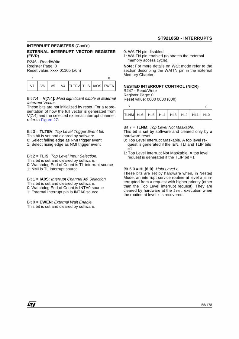
55/178
ST92185B - INTERRUPTS
INTERRUPT REGISTERS (Cont’d)
EXTERNAL INTERRUPT VECTOR REGISTER(EIVR)
R246 - Read/WriteRegister Page: 0Reset value: xxxx 0110b (x6h)
Bit 7:4 = V[7:4]: Most significant nibble of ExternalInterrupt Vector. These bits are not initialized by reset. For a repre-sentation of how the full vector is generated fromV[7:4] and the selected external interrupt channel,refer to Figure 27.
Bit 3 = TLTEV: Top Level Trigger Event bit. This bit is set and cleared by software.0: Select falling edge as NMI trigger event 1: Select rising edge as NMI trigger event
Bit 2 = TLIS: Top Level Input Selection.This bit is set and cleared by software.0: Watchdog End of Count is TL interrupt source1: NMI is TL interrupt source
Bit 1 = IA0S: Interrupt Channel A0 Selection.This bit is set and cleared by software.0: Watchdog End of Count is INTA0 source1: External Interrupt pin is INTA0 source
Bit 0 = EWEN: External Wait Enable.This bit is set and cleared by software.
0: WAITN pin disabled1: WAITN pin enabled (to stretch the external
memory access cycle).
Note: For more details on Wait mode refer to thesection describing the WAITN pin in the ExternalMemory Chapter.
NESTED INTERRUPT CONTROL (NICR)R247 - Read/WriteRegister Page: 0Reset value: 0000 0000 (00h)
Bit 7 = TLNM: Top Level Not Maskable.This bit is set by software and cleared only by ahardware reset.0: Top Level Interrupt Maskable. A top level re-
quest is generated if the IEN, TLI and TLIP bits =1
1: Top Level Interrupt Not Maskable. A top level request is generated if the TLIP bit =1
Bit 6:0 = HL[6:0]: Hold Level x These bits are set by hardware when, in NestedMode, an interrupt service routine at level x is in-terrupted from a request with higher priority (otherthan the Top Level interrupt request). They arecleared by hardware at the iret execution whenthe routine at level x is recovered.
7 0
V7 V6 V5 V4 TLTEV TLIS IAOS EWEN
7 0
TLNM HL6 HL5 HL4 HL3 HL2 HL1 HL0

56/178
ST92185B - INTERRUPTS
INTERRUPT REGISTERS (Cont’d)
EXTERNAL MEMORY REGISTER 2 (EMR2)
R246 - Read/WriteRegister Page: 21Reset value: 0000 1111 (0Fh)
Bit 7, 5:0 = Reserved, keep in reset state. Refer tothe external Memory Interface Chapter.
Bit 6 = ENCSR: Enable Code Segment Register.This bit is set and cleared by software. It affectsthe ST9 CPU behaviour whenever an interrupt re-quest is issued. 0: The CPU works in original ST9 compatibility
mode. For the duration of the interrupt service routine, ISR is used instead of CSR, and the in-terrupt stack frame is identical to that of the orig-inal ST9: only the PC and Flags are pushed. This avoids saving the CSR on the stack in the event of an interrupt, thus ensuring a faster in-
terrupt response time. The drawback is that it is not possible for an interrupt service routine to perform inter-segment calls or jumps: these in-structions would update the CSR, which, in this case, is not used (ISR is used instead). The code segment size for all interrupt service rou-tines is thus limited to 64K bytes.
1: ISR is only used to point to the interrupt vector table and to initialize the CSR at the beginning of the interrupt service routine: the old CSR is pushed onto the stack together with the PC and flags, and CSR is then loaded with the contents of ISR. In this case, iret will also restore CSR from the stack. This approach allows interrupt service routines to access the entire 4 Mbytes of address space; the drawback is that the inter-rupt response time is slightly increased, be-cause of the need to also save CSR on the stack. Full compatibility with the original ST9 is lost in this case, because the interrupt stack frame is different; this difference, however, should not affect the vast majority of programs.
7 0
0 ENCSR 0 0 1 1 1 1

57/178
ST92185B - RESET AND CLOCK CONTROL UNIT (RCCU)
4 RESET AND CLOCK CONTROL UNIT (RCCU)
4.1 INTRODUCTION
The Reset Control Unit comprises two distinct sec-tions:
– An oscillator that uses an external quartz crystal.
– The Reset/Stop Manager, which detects and flags Hardware, Software and Watchdog gener-ated resets.
4.2 RESET / STOP MANAGER
The RESET/STOP Manager resets the devicewhen one of the three following triggering eventsoccurs:
– A hardware reset, consequence of a low level on the RESET pin.
– A software reset, consequence of an HALT in-struction when enabled.
– A Watchdog end of count.
The RESET input is schmitt triggered.
Note: The memorized Internal Reset (called RE-SETO) will be maintained active for a duration of32768 Oscin periods (about 8 ms for a 4 MHz crys-tal) after the external input is released (set high).
This RESETO internal Reset signal is output onthe I/O port bit P3.7 (active low) during the wholereset phase until the P3.7 configuration is changedby software. The true internal reset (to all macro-cells) will only be released 511 Reference clockperiods after the Memorized Internal reset is re-leased.
It is possible to know which was the last RESETtriggering event, by reading bits 5 and 6 of registerSDRATH.
Figure 29. Reset Overviewn
Build-up CounterRCCU
TrueRESET
RESETOMemorized
Reset
InternalReset

58/178
ST92185B - RESET AND CLOCK CONTROL UNIT (RCCU)
4.3 OSCILLATOR CHARACTERISTICS
The on-chip oscillator circuit uses an inverting gatecircuit with tri-state output.
Notes: Owing to the Q factor required, CeramicResonators may not provide a reliable oscillatorsource.
The oscillator can not support quartz crystal or ce-ramic working at the third harmonic without exter-nal tank circuits.
OSCOUT must not be used to drive external cir-cuits.
Halt mode is set by means of the HALT instruction.In this mode the parallel resistor, R, is disconnect-ed and the oscillator is disabled. This forces the in-ternal clock to a high level and OSCOUT to a highimpedance state.
To exit the HALT condition and restart the oscilla-tor, an external RESET pulse is required.
It should be noted that, if the Watchdog function isenabled, a HALT instruction will not disable the os-cillator. This to avoid stopping the Watchdog if aHALT code is executed in error. When this occurs,the CPU will be reset when the Watchdog timesout or when an external reset is applied.
When an HALT instruction is executed, the maincrystal oscillator is stoped and any spurious clockare ignored. Other analog systems such as the on-chip line PLL or the whole Video chain (Sync Ex-traction) must be stopped separately by the soft-ware as they will induce static consumption.
Table 8. Oscillator Transconductance
Figure 30. Crystal Oscillator
Note: Depending on the application it may be bet-ter not to implement CL1
Figure 31. Internal Oscillator Schematic
Figure 32. External Clockn
gm Min Typ Max
mA/V 0.77 1.5 2.4
OSCIN OSCOUT
CL1 CL2
ST9
CRYSTAL CLOCK
VR02116A
VR02086A
HALT
OSCIN OSCOUT
RIN ROUT
R
OSCIN OSCOUT
CLOCKINPUT
NC
EXTERNAL CLOCK
VR02116B
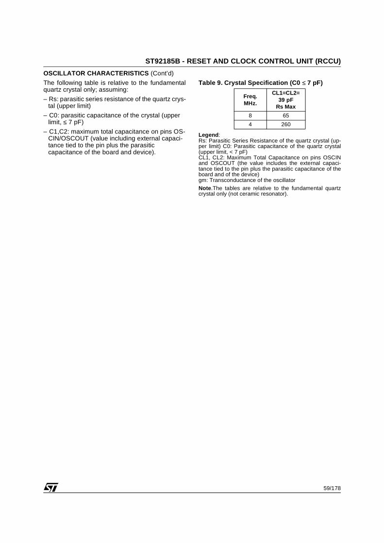
59/178
ST92185B - RESET AND CLOCK CONTROL UNIT (RCCU)
OSCILLATOR CHARACTERISTICS (Cont’d)
The following table is relative to the fundamentalquartz crystal only; assuming:
– Rs: parasitic series resistance of the quartz crys-tal (upper limit)
– C0: parasitic capacitance of the crystal (upper limit, ≤ 7 pF)
– C1,C2: maximum total capacitance on pins OS-CIN/OSCOUT (value including external capaci-tance tied to the pin plus the parasitic capacitance of the board and device).
Table 9. Crystal Specification (C0 ≤ 7 pF)
Legend:Rs: Parasitic Series Resistance of the quartz crystal (up-per limit) C0: Parasitic capacitance of the quartz crystal(upper limit, < 7 pF)CL1, CL2: Maximum Total Capacitance on pins OSCINand OSCOUT (the value includes the external capaci-tance tied to the pin plus the parasitic capacitance of theboard and of the device)gm: Transconductance of the oscillator
Note.The tables are relative to the fundamental quartzcrystal only (not ceramic resonator).
Freq. MHz.
CL1=CL2=39 pF
Rs Max
8 65
4 260

60/178
ST92185B - RESET AND CLOCK CONTROL UNIT (RCCU)
4.4 CLOCK CONTROL REGISTERS
MODE REGISTER (MODER)R235 - Read/WriteRegister Group: E (System)Reset Value: 1110 0000 (E0h)
Bit 7:6 = Bits described in Device Architecturechapter.
Bit 5 = DIV2: OSCIN Divided by 2. This bit controls the divide by 2 circuit which oper-ates on the OSCIN Clock.0: No division of OSCIN Clock1: OSCIN clock is internally divided by 2
Bit 4:2 = PRS[2:0]: Clock Prescaling.These bits define the prescaler value used toprescale CPUCLK from INTCLK. When they arereset, the CPUCLK is not prescaled, and is equalto INTCLK; in all other cases, the internal clock isprescaled by the value of these three bits plus one.
Bit 1:0 = Bits described in Device Architecturechapter.
WAIT CONTROL REGISTER (WCR) R252 - Read/WriteRegister Page: 0Reset Value: 0111 1111 (7Fh)
Bit 7 = Reserved, read as “0”.
Bit 6 = WDGEN: refer to Timer/Watchdog chapter.
WARNING. Resetting this bit to zero has the effectof setting the Timer/Watchdog to the Watchdogmode. Unless this is desired, this must be set to“1”.
Bit 5:3 = WDM[2:0]: Data Memory Wait Cycles.These bits contain the number of INTCLK cyclesto be added automatically to external Data memo-ry accesses. WDM = 0 gives no additional wait cy-cles. WDM = 7 provides the maximum 7 INTCLKcycles (reset condition).
Bit 2:0 = WPM[2:0]: Program Memory Wait Cy-cles.These bits contain the number of INTCLK cyclesto be added automatically to external Programmemory accesses. WPM = 0 gives no additionalwait cycles, WPM = 7 provides the maximum 7INTCLK cycles (reset condition).
Note: The number of clock cycles added refers toINTCLK and NOT to CPUCLK.
WARNING. The reset value of the Wait ControlRegister gives the maximum number of Wait cy-cles for external memory. To get optimum per-formance from the ST9 when used in single-chipmode (no external memory) the user should writethe WDM2,1,0 and WPM2,1,0 bits to “0”.
7 0
1 1 DIV2 PRS2 PRS1 PRS0 0 0
7 0
0 WDGEN WDM2 WDM1 WDM0 WPM2 WPM1 WPM0

61/178
ST92185B - RESET AND CLOCK CONTROL UNIT (RCCU)
4.5 RESET CONTROL UNIT REGISTERS
The RCCU consists of two registers. They arePCONF and SDRATH. Unless otherwise stated,unused register bits must be kept in their reset val-ue in order to avoid problems with the device be-haviour.
PLL CONFIGURATION REGISTER (PCONF)R251 - Read/WriteRegister Page: 55Reset value: 0000 0111 (07h)
Bit 7= SRESEN. Software Reset Enable.0: RCCU PLL and CSDU are turned off when a
HALT instruction is performed.1: RCCU will reset the microcontroller when a
HALT instruction is performed.
Bit 6:0= Reserved bits. Leave in their reset state.
CLOCK SLOW DOWN UNIT RATIO REGISTER(SDRATH)R254 - Read/WriteRegister Page: 55Reset value:0010 0xxx (2xh) after software reset0100 0xxx (4xh) after watchdog reset0000 0000 (00h) after external reset
Bit 7 = Reserved bit. Leave in its reset state.
Bit 6 = WDGRES. Watchdog Reset. WDGRES isautomatically set if the last reset was a watchdogReset. This is a read only bit.
Bit 5 = SFTRES. Software Reset. SFTRES is au-tomatically set if the last reset was a software Re-set. This is a read only bit.
Bit 4:0 = Reserved bits. Please leave in their resetstate.
7 0
SRESEN 0 0 0 0 1 1 1
7 0
0 WDGRES SFTRES 0 0 x x x

62/178
ST92185B - TIMING AND CLOCK CONTROLLER
5 TIMING AND CLOCK CONTROLLER
5.1 FREQUENCY MULTIPLIERS
Three on-chip frequency multipliers generate theproper frequencies for: the Core/Real time Periph-erals, the Display related time base.
For both the Core and the Display frequency mul-tipliers, a 4 bit programmable feed-back counterallows the adjustment of the multiplying factor tothe application need (a 4 MHz or 8 MHz crystal isassumed).
Figure 33. Timing and Clock Controller Block Diagram
Frequency Multiplier
FML(3:0)FMEN
XtalOscillator
Asynch.Handler
FMSLMain Clock Controller
Divide by 2
MCFM
OSCIN
OSCOUT
Fimf
Divide by 2
SLDIV2
FMEN
Frequency Multiplier
Skew Corrector Synchronized DOTCK / 2 to Display
SKWL(3:0)SKWEN
HsyncSKHPLS
PXFM
(Synchronized DOTCK)
Divideby 2
(2X Pixel clock for 1X width characters)
4 MHz real time
Divideby 2 to Display Storage RAM (TRI)
Div-2
MODER.5
SKDIV2
SKDIV2
VR02095A
Async. Handler
Memory WaitBREQ
WFI
CPUCLKPrescaler 1 to 8
ClockControl
INTCLK
ST9 Clock Control Unit (RCCU)

63/178
ST92185B - TIMING AND CLOCK CONTROLLER
FREQUENCY MULTIPLIERS (Cont’d)
For the Off-chip filter components please refer tothe Required External Components figure provid-ed in the first section of the data sheet.
The frequency multipliers are off during and uponexiting from the reset phase. The user must pro-gram the desired multiplying factor, start the multi-plier and then wait for its stability.
Once the Core/Peripherals multiplier is stabilized,the Main Clock controller can be re-programmed(through the FMSL bit, MCCR.6) to provide the fi-nal frequency (INTCLK) to the CPU.
The frequency multipliers are automaticallyswitched off when the µP enters in HALT mode(the HALT mode forces the control register to itsreset status).Table 10. Examples of CPU speed choice
Note: 24 MHz is the max. CPU authorized frequency.
Table 11. DOTCK/2 frequency choices
(*) Preferred values for 4/3.
(**) 16/9 screen formats.
Note: 18 MHz is the min. DOTCK/2 authorized frequency.
Table 12. External PLL Filter Stabilisation time
Crystal Frequency
FML(3:0)
Internal Frequency(Fimf)
4 MHz 4 10 MHz
4 MHz 5 12 MHz
4 MHz 6 14 MHz
4 MHz 7 16 MHz
4 MHz 8 18 MHz
4 MHz 11 24 MHz
SKW(3:0)
DOTCK/2
8 18 MHz
9 20 MHz(*)
10 22 MHz
11 24 MHz (**)
Clock Pin Name Clock Name Control Register Stabilization PeriodMCFM Main Clock PLL Filter Input Pin MCCR 35 ms.
PXFM Pixel Clock PLL Filter Input Pin PXCCR 35 ms

64/178
ST92185B - TIMING AND CLOCK CONTROLLER
Figure 34. Programming the MCCR
Figure 35. Programming the SKCCR, PXCCR
Set the PLL frequency
FML (3:0)
Start the PLL by setting
FMEN = 1
Validate PLL as Main
CPU Clock
Wait for Clock Stabilization
Example:
spp #27h ;Set the page
ld MCCR, #04h ;Set FML bits to the value needed e.g. 10 MHz
or MCCR, #80h ;Starts the PLL
or MCCR, #40h ;Validate the PLL as the main CPU Clock
Wait for stabilization time
Set the PLL frequency
SKW (3:0)
Start the PLL by setting
SKWEN = 1
Validate PLL is fed to
TDSRAM and OSD
Wait for Clock Stabilization
Example:
spp #27h ;Set the page
ld SKCCR, #04h ;Set SKW bits to the value needed
or SKCCR, #80h ;Starts the PLL
or PXCCR, #80h ;PLL is fed as DOTCK to the TDSRAM & OSDPLL
Wait for stabilization time

65/178
ST92185B - TIMING AND CLOCK CONTROLLER
5.2 REGISTER DESCRIPTION
MAIN CLOCK CONTROL REGISTER (MCCR)R253 - Read/ WriteRegister Page: 39Reset value: 0000 0000 (00h)
The HALT mode forces the register to its initializa-tion state.
Bit 7 = FMEN. Frequency Multiplier Enable bit.0: FM disabled (reset state), low-power consump-
tion mode.1: FM is enabled, providing clock to the CPU. The
FMEN bit must be set only after programming the FML(3:0) bits.
Bit 6= FMSL. Frequency Multiplier Select bit.This bit controls the choice of the ST9+ core inter-nal frequency between the external crystal fre-quency and the Main Clock issued by the frequen-cy multiplier.
In order to secure the application, the ST9+ coreinternal frequency is automatically switched backto the external crystal frequency if the frequencymultiplier is switched off (FMEN =0) regardless ofthe value of the FMSL bit. Care must be taken toreset the FMSL bit before any frequency multipliercan restart (FMEN set back to 1).
After reset, the external crystal frequency is al-ways sent to the ST9+ Core.
Bit 5:4 = These bits are reserved.
Bit 3:0 = FML[3:0] Frequency bits. These 4 bits program the down-counter inserted inthe feed-back loop of the Frequency Multiplierwhich generates the internal multiplied frequencyFimf. The Fimf value is calculated as follows :
Fimf = Crystal frequency * [ (FML(3:0) + 1) ] /2
SKEW CLOCK CONTROL REGISTER (SKCCR)R254 - Read/ WriteRegister Page: 39Reset value: 0000 0000 (00h)
The HALT mode forces the register to its initializa-tion state.
Bit 7= SKWEN. Frequency Multiplier Enable bit. 0: FM disabled (reset state), low-power consump-
tion mode.1: FM is enabled, supplying the clock to the Skew
corrector. The SKWEN bit must be set only after programming the SKW(3-0) bits.
Bit 6= SKDIV2. Divide-by-2 enableThis bit determines whether a divide-by-2 down-scaling factor is applied to the output of the SkewCorrector. 0 = Divide-by-2 enabled1 = Divide-by-2 disabled
Bit 5:4 = These bits are reserved.
Bit 3:0 = SKW[3:0]. Frequency bitsThese 4 bits program the down-counter inserted inthe feedback loop of the Frequency Multiplierwhich generates the internal multiplied frequencyDOTCK. The DOTCK value is calculated as fol-lows :
F(DOTCK) = Crystal frequency * [ (SKW(3:0) + 1) ]
7 6 5 4 3 2 1 0
FMEN FMSL 0 0 FML3 FML2 FML1 FML0
7 6 5 4 3 2 1 0
SKWEN
SKDIV2 0 0 SKW3 SKW2 SKW1 SKW0

66/178
ST92185B - TIMING AND CLOCK CONTROLLER
REGISTER DESCRIPTION (Cont’d)
PLL CLOCK CONTROL REGISTER (PXCCR)R251 - Read/WriteRegister Page: 39Reset value: 0000 0000 (00h)
Bit 7= PXCE. Pixel Clock Enable bit.0: Pixel and TDSRAM interface clocks are blocked1: Pixel clock is sent to the display controller and
TDSRAM interface.
Bit 6:0= These bits are reserved.
SLICER CLOCK CONTROL REGISTER(SLCCR)R252 - Read/ WriteRegister Page: 39Reset value: 0000 0000 (00h)
The HALT mode forces the register to its initializa-tion state.
Bit 7:5 = These bits are reserved.
Bit 4= VMOD: Video mode selection.This bit is used to select either 50Hz or 60Hz videomode. It is set and cleared by software. 0: 50 Hz.1: 60 Hz.
Bit 3:0= These bits are reserved.
5.2.1 Register MappingThe Timing Controller has 4 dedicated registers,mapped in a ST9+ register file page (the page ad-dress is 39 (27h)), as follows :
7 6 5 4 3 2 1 0
PXCE 0 0 0 0 0 0 0
7 6 5 4 3 2 1 0
0 0 0 VMOD 0 0 0 0
Page 39 (27h)
FEh Skew Corrector Control Register SKCCR
FDh Main Clock Control Register MCCR
FCh SLicer Clock Control Register SLCCR
FBh Pixel Clock Control Register PXCCR

67/178
ST92185B - I/O PORTS
6 I/O PORTS
6.1 INTRODUCTION
ST9 devices feature flexible individually program-mable multifunctional input/output lines. Refer tothe Pin Description Chapter for specific pin alloca-tions. These lines, which are logically grouped as8-bit ports, can be individually programmed to pro-vide digital input/output and analog input, or toconnect input/output signals to the on-chip periph-erals as alternate pin functions. All ports can be in-dividually configured as an input, bi-directional,output or alternate function. In addition, pull-upscan be turned off for open-drain operation, andweak pull-ups can be turned on in their place, toavoid the need for off-chip resistive pull-ups. Portsconfigured as open drain must never have voltageon the port pin exceeding VDD (refer to the Electri-cal Characteristics section). Depending on thespecific port, input buffers are software selectableto be TTL or CMOS compatible, however on Sch-mitt trigger ports, no selection is possible.
6.2 SPECIFIC PORT CONFIGURATIONS
Refer to the Pin Description chapter for a list of thespecific port styles and reset values.
6.3 PORT CONTROL REGISTERS
Each port is associated with a Data register(PxDR) and three Control registers (PxC0, PxC1,PxC2). These define the port configuration and al-low dynamic configuration changes during pro-gram execution. Port Data and Control registersare mapped into the Register File as shown in Fig-ure 1. Port Data and Control registers are treatedjust like any other general purpose register. Thereare no special instructions for port manipulation:any instruction that can address a register, can ad-dress the ports. Data can be directly accessed inthe port register, without passing through othermemory or “accumulator” locations.
Figure 36. I/O Register Map
GROUP E GROUP FPAGE 2
GROUP FPAGE 3
GROUP FPAGE 43
SystemRegisters
FFh Reserved P7DR P9DR R255
FEh P3C2 P7C2 P9C2 R254
FDh P3C1 P7C1 P9C1 R253
FCh P3C0 P7C0 P9C0 R252
FBh Reserved P6DR P8DR R251
FAh P2C2 P6C2 P8C2 R250
F9h P2C1 P6C1 P8C1 R249
F8h P2C0 P6C0 P8C0 R248
F7h Reserved Reserved
Reserved
R247
F6h P1C2 P5C2 R246
E5h P5DR R229 F5h P1C1 P5C1 R245
E4h P4DR R228 F4h P1C0 P5C0 R244
E3h P3DR R227 F3h Reserved Reserved R243
E2h P2DR R226 F2h P0C2 P4C2 R242
E1h P1DR R225 F1h P0C1 P4C1 R241
E0h P0DR R224 F0h P0C0 P4C0 R240

68/178
ST92185B - I/O PORTS
PORT CONTROL REGISTERS (Cont’d)
During Reset, ports with weak pull-ups are set inbidirectional/weak pull-up mode and the outputData Register is set to FFh. This condition is alsoheld after Reset, except for Ports 0 and 1 in ROM-less devices, and can be redefined under softwarecontrol.
Bidirectional ports without weak pull-ups are set inhigh impedance during reset. To ensure properlevels during reset, these ports must be externallyconnected to either VDD or VSS through externalpull-up or pull-down resistors.
Other reset conditions may apply in specific ST9devices.
6.4 INPUT/OUTPUT BIT CONFIGURATION
By programming the control bits PxC0.n andPxC1.n (see Figure 2) it is possible to configure bitPx.n as Input, Output, Bidirectional or AlternateFunction Output, where X is the number of the I/Oport, and n the bit within the port (n = 0 to 7).
When programmed as input, it is possible to selectthe input level as TTL or CMOS compatible by pro-gramming the relevant PxC2.n control bit.This option is not available on Schmitt trigger ports.
The output buffer can be programmed as push-pull or open-drain.
A weak pull-up configuration can be used to avoidexternal pull-ups when programmed as bidirec-tional (except where the weak pull-up option hasbeen permanently disabled in the pin hardware as-signment).
Each pin of an I/O port may assume software pro-grammable Alternate Functions (refer to the de-vice Pin Description and to Section 1.5). To outputsignals from the ST9 peripherals, the port must beconfigured as AF OUT. On ST9 devices with A/DConverter(s), configure the ports used for analoginputs as AF IN.
The basic structure of the bit Px.n of a general pur-pose port Px is shown in Figure 3.
Independently of the chosen configuration, whenthe user addresses the port as the destination reg-ister of an instruction, the port is written to and thedata is transferred from the internal Data Bus tothe Output Master Latches. When the port is ad-dressed as the source register of an instruction,the port is read and the data (stored in the InputLatch) is transferred to the internal Data Bus.
When Px.n is programmed as an Input: (See Figure 4).– The Output Buffer is forced tristate.– The data present on the I/O pin is sampled into
the Input Latch at the beginning of each instruc-tion execution.
– The data stored in the Output Master Latch iscopied into the Output Slave Latch at the end ofthe execution of each instruction. Thus, if bit Px.nis reconfigured as an Output or Bidirectional, thedata stored in the Output Slave Latch will be re-flected on the I/O pin.

69/178
ST92185B - I/O PORTS
INPUT/OUTPUT BIT CONFIGURATION (Cont’d)
Figure 37. Control Bits
n
Table 13. Port Bit Configuration Table (n = 0, 1... 7; X = port number)
(1) For A/D Converter inputs.
Legend:X = Port n = BitAF = Alternate FunctionBID = BidirectionalCMOS= CMOS Standard Input LevelsHI-Z = High ImpedanceIN = InputOD = Open DrainOUT = OutputPP = Push-PullTTL = TTL Standard Input LevelsWP = Weak Pull-up
Bit 7 Bit n Bit 0
PxC2 PxC27 PxC2n PxC20
PxC1 PxC17 PxC1n PxC10
PxC0 PxC07 PxC0n PxC00
General Purpose I/O Pins A/D Pins
PXC2nPXC1nPXC0n
000
100
010
110
001
101
011
111
111
PXn Configuration BID BID OUT OUT IN IN AF OUT AF OUT AF IN
PXn Output Type WP OD OD PP OD HI-Z HI-Z PP OD HI-Z(1)
PXn Input TypeTTL
(or Schmitt
Trigger)
TTL(or Schmitt
Trigger)
TTL(or Schmitt
Trigger)
TTL(or Schmitt
Trigger)
CMOS(or Schmitt
Trigger)
TTL(or Schmitt
Trigger)
TTL(or Schmitt
Trigger)
TTL(or Schmitt
Trigger)
Analog Input

70/178
ST92185B - I/O PORTS
INPUT/OUTPUT BIT CONFIGURATION (Cont’d)
Figure 38. Basic Structure of an I/O Port Pin
Figure 39. Input Configuration
nn
Figure 40. Output Configuration
n
OUTPUT SLAVE LATCH
OUTPUT MASTER LATCH INPUT LATCH
INTERNAL DATA BUS
I/O PIN
PUSH-PULLTRISTATE
OPEN DRAINWEAK PULL-UP
FROMPERIPHERAL
OUTPUTOUTPUT
INPUTBIDIRECTIONAL
ALTERNATEFUNCTION
TO PERIPHERALINPUTS AND
TTL / CMOS(or Schmitt Trigger)
INTERRUPTSALTERNATEFUNCTION
INPUTOUTPUT
BIDIRECTIONAL
OUTPUT MASTER LATCH INPUT LATCH
OUTPUT SLAVE LATCH
INTERNAL DATA BUS
I/O PIN
TRISTATE
TO PERIPHERAL
INPUTS AND
TTL / CMOS
(or Schmitt Trigger)
INTERRUPTS
OUTPUT MASTER LATCH INPUT LATCH
OUTPUT SLAVE LATCH
INTERNAL DATA BUS
I/O PIN
OPEN DRAIN TTL
(or Schmitt Trigger)PUSH-PULL
TO PERIPHERAL
INPUTS AND
INTERRUPTS

71/178
ST92185B - I/O PORTS
INPUT/OUTPUT BIT CONFIGURATION (Cont’d)
When Px.n is programmed as an Output: (Figure 5)
– The Output Buffer is turned on in an Open-drainor Push-pull configuration.
– The data stored in the Output Master Latch iscopied both into the Input Latch and into the Out-put Slave Latch, driving the I/O pin, at the end ofthe execution of the instruction.
When Px.n is programmed as Bidirectional:(Figure 6)
– The Output Buffer is turned on in an Open-Drainor Weak Pull-up configuration (except when dis-abled in hardware).
– The data present on the I/O pin is sampled intothe Input Latch at the beginning of the executionof the instruction.
– The data stored in the Output Master Latch iscopied into the Output Slave Latch, driving the I/O pin, at the end of the execution of the instruc-tion.
WARNING: Due to the fact that in bidirectionalmode the external pin is read instead of the outputlatch, particular care must be taken with arithme-tic/logic and Boolean instructions performed on abidirectional port pin.
These instructions use a read-modify-write se-quence, and the result written in the port registerdepends on the logical level present on the exter-nal pin.
This may bring unwanted modifications to the portoutput register content.
For example:
Port register content, 0Fh external port value, 03h(Bits 3 and 2 are externally forced to 0)
A bset instruction on bit 7 will return:
Port register content, 83hexternal port value, 83h(Bits 3 and 2 have been cleared).
To avoid this situation, it is suggested that all oper-ations on a port, using at least one bit in bidirec-tional mode, are performed on a copy of the portregister, then transferring the result with a load in-struction to the I/O port.
When Px.n is programmed as a digital Alter-nate Function Output:(Figure 7)
– The Output Buffer is turned on in an Open-Drainor Push-Pull configuration.
– The data present on the I/O pin is sampled intothe Input Latch at the beginning of the executionof the instruction.
– The signal from an on-chip function is allowed toload the Output Slave Latch driving the I/O pin.Signal timing is under control of the alternatefunction. If no alternate function is connected toPx.n, the I/O pin is driven to a high level when inPush-Pull configuration, and to a high imped-ance state when in open drain configuration.
Figure 41. Bidirectional Configuration
nn
Figure 42. Alternate Function Configuration
nnnnnn
OUTPUT MASTER LATCH INPUT LATCH
OUTPUT SLAVE LATCH
INTERNAL DATA BUS
I/O PIN
WEAK PULL-UP TTL
(or Schmitt Trigger)OPEN DRAIN
TO PERIPHERALINPUTS AND
INTERRUPTS
INPUT LATCH
FROM
INTERNAL DATA BUS
I/O PIN
OPEN DRAIN TTL
(or Schmitt Trigger)PUSH-PULL
PERIPHERALOUTPUT
TO PERIPHERALINPUTS AND
INTERRUPTSOUTPUT SLAVE LATCH

72/178
ST92185B - I/O PORTS
6.5 ALTERNATE FUNCTION ARCHITECTURE
Each I/O pin may be connected to three differenttypes of internal signal:
– Data bus Input/Output
– Alternate Function Input
– Alternate Function Output
6.5.1 Pin Declared as I/O
A pin declared as I/O, is connected to the I/O buff-er. This pin may be an Input, an Output, or a bidi-rectional I/O, depending on the value stored in(PxC2, PxC1 and PxC0).
6.5.2 Pin Declared as an Alternate FunctionInput
A single pin may be directly connected to severalAlternate Function inputs. In this case, the usermust select the required input mode (with thePxC2, PxC1, PxC0 bits) and enable the selectedAlternate Function in the Control Register of theperipheral. No specific port configuration is re-quired to enable an Alternate Function input, sincethe input buffer is directly connected to each alter-nate function module on the shared pin. As morethan one module can use the same input, it is up tothe user software to enable the required moduleas necessary. Parallel I/Os remain operationaleven when using an Alternate Function input. Theexception to this is when an I/O port bit is perma-nently assigned by hardware as an A/D bit. In thiscase , after software programming of the bit in AF-OD-TTL, the Alternate function output is forced tologic level 1. The analog voltage level on the cor-responding pin is directly input to the A/D (See Fig-ure 8).
Figure 43. A/D Input Configuration
6.5.3 Pin Declared as an Alternate FunctionOutputThe user must select the AF OUT configurationusing the PxC2, PxC1, PxC0 bits. Several Alter-nate Function outputs may drive a common pin. Insuch case, the Alternate Function output signalsare logically ANDed before driving the commonpin. The user must therefore enable the requiredAlternate Function Output by software.
WARNING: When a pin is connected both to an al-ternate function output and to an alternate functioninput, it should be noted that the output signal willalways be present on the alternate function input.
6.6 I/O STATUS AFTER WFI, HALT AND RESET
The status of the I/O ports during the Wait For In-terrupt, Halt and Reset operational modes isshown in the following table. The External MemoryInterface ports are shown separately. If only the in-ternal memory is being used and the ports are act-ing as I/O, the status is the same as shown for theother I/O ports.
INPUT LATCH
INTERNAL DATA BUS
I/O PIN
TRISTATE
INPUTBUFFEROUTPUT SLAVE LATCH
OUTPUT MASTER LATCH
TOWARDS A/D CONVERTER
GND
ModeExt. Mem - I/O Ports
I/O PortsP0
P1, P2, P6, P9
WFI
High Imped-ance or next address (de-pending on
the last memory op-eration per-formed on
Port)
NextAddress
Not Affected (clock outputs running)
HALTHigh Imped-
anceNext
AddressNot Affected (clock outputs stopped)
RESETAlternate function push-pull (ROMless device)
Bidirectional Weak Pull-up (High im-pedance when disa-bled in hardware).

73/178
ST92185B - TIMER/WATCHDOG (WDT)
7 ON-CHIP PERIPHERALS
7.1 TIMER/WATCHDOG (WDT)
Important Note: This chapter is a generic descrip-tion of the WDT peripheral. However dependingon the ST9 device, some or all of WDT interfacesignals described may not be connected to exter-nal pins. For the list of WDT pins present on theST9 device, refer to the device pinout descriptionin the first section of the data sheet.
7.1.1 Introduction
The Timer/Watchdog (WDT) peripheral consists ofa programmable 16-bit timer and an 8-bit prescal-er. It can be used, for example, to:
– Generate periodic interrupts
– Measure input signal pulse widths
– Request an interrupt after a set number of events
– Generate an output signal waveform
– Act as a Watchdog timer to monitor system in-tegrity
The main WDT registers are:
– Control register for the input, output and interrupt logic blocks (WDTCR)
– 16-bit counter register pair (WDTHR, WDTLR)
– Prescaler register (WDTPR)
The hardware interface consists of up to five sig-nals:
– WDIN External clock input
– WDOUT Square wave or PWM signal output
– INT0 External interrupt input
– NMI Non-Maskable Interrupt input
– HW0SW1 Hardware/Software Watchdog ena-ble.
Figure 44. Timer/Watchdog Block Diagram
INT01
INPUT
&
CLOCK CONTROL LOGIC
INEN INMD1 INMD2
WDTPR8-BIT PRESCALER
WDTRH, WDTRL16-BIT
INTCLK/4
WDT
OUTMD WROUT
OUTPUT CONTROL LOGIC
INTERRUPT
CONTROL LOGIC
END OFCOUNT
RESET
TOP LEVEL INTERRUPT REQUEST
OUTEN
MUX
WDOUT1
IAOSTLIS
INTA0 REQUEST
NMI1
WDGEN
HW0SW11
WDIN1
MUX
DOWNCOUNTERCLOCK
1Pin not present on some ST9 devices.

74/178
ST92185B - TIMER/WATCHDOG (WDT)
TIMER/WATCHDOG (Cont’d)
7.1.2 Functional Description
7.1.2.1 External SignalsThe HW0SW1 pin can be used to permanently en-able Watchdog mode. Refer to Section 0.1.3.1.
The WDIN Input pin can be used in one of fourmodes:
– Event Counter Mode
– Gated External Input Mode
– Triggerable Input Mode
– Retriggerable Input Mode
The WDOUT output pin can be used to generate asquare wave or a Pulse Width Modulated signal.
An interrupt, generated when the WDT is runningas the 16-bit Timer/Counter, can be used as a TopLevel Interrupt or as an interrupt source connectedto channel A0 of the external interrupt structure(replacing the INT0 interrupt input).
The counter can be driven either by an externalclock, or internally by INTCLK divided by 4.
7.1.2.2 InitialisationThe prescaler (WDTPR) and counter (WDTRL,WDTRH) registers must be loaded with initial val-ues before starting the Timer/Counter. If this is notdone, counting will start with reset values.
7.1.2.3 Start/Stop
The ST_SP bit enables downcounting. When thisbit is set, the Timer will start at the beginning of thefollowing instruction. Resetting this bit stops thecounter.
If the counter is stopped and restarted, countingwill resume from the last value unless a new con-stant has been entered in the Timer registers(WDTRL, WDTRH).
A new constant can be written in the WDTRH,WDTRL, WDTPR registers while the counter isrunning. The new value of the WDTRH, WDTRLregisters will be loaded at the next End of Count(EOC) condition while the new value of theWDTPR register will be effective immediately.
End of Count is when the counter is 0.
When Watchdog mode is enabled the state of theST_SP bit is irrelevant.
7.1.2.4 Single/Continuous Mode
The S_C bit allows selection of single or continu-ous mode.This Mode bit can be written with theTimer stopped or running. It is possible to togglethe S_C bit and start the counter with the same in-struction.
Single Mode
On reaching the End Of Count condition, the Timerstops, reloads the constant, and resets the Start/Stop bit. Software can check the current status byreading this bit. To restart the Timer, set the Start/Stop bit.
Note: If the Timer constant has been modified dur-ing the stop period, it is reloaded at start time.
Continuous ModeOn reaching the End Of Count condition, the coun-ter automatically reloads the constant and restarts.It is stopped only if the Start/Stop bit is reset.
7.1.2.5 Input SectionIf the Timer/Counter input is enabled (INEN bit) itcan count pulses input on the WDIN pin. Other-wise it counts the internal clock/4.
For instance, when INTCLK = 24MHz, the End OfCount rate is:
2.79 seconds for Maximum Count (Timer Const. = FFFFh, Prescaler Const. = FFh)
166 ns for Minimum Count (Timer Const. = 0000h, Prescaler Const. = 00h)
The Input pin can be used in one of four modes:
– Event Counter Mode
– Gated External Input Mode
– Triggerable Input Mode
– Retriggerable Input Mode
The mode is configurable in the WDTCR.
7.1.2.6 Event Counter ModeIn this mode the Timer is driven by the externalclock applied to the input pin, thus operating as anevent counter. The event is defined as a high tolow transition of the input signal. Spacing betweentrailing edges should be at least 8 INTCLK periods(or 333ns with INTCLK = 24MHz).
Counting starts at the next input event after theST_SP bit is set and stops when the ST_SP bit isreset.

75/178
ST92185B - TIMER/WATCHDOG (WDT)
TIMER/WATCHDOG (Cont’d)
7.1.2.7 Gated Input Mode
This mode can be used for pulse width measure-ment. The Timer is clocked by INTCLK/4, and isstarted and stopped by means of the input pin andthe ST_SP bit. When the input pin is high, the Tim-er counts. When it is low, counting stops. Themaximum input pin frequency is equivalent toINTCLK/8.
7.1.2.8 Triggerable Input Mode
The Timer (clocked internally by INTCLK/4) isstarted by the following sequence:
– setting the Start-Stop bit, followed by
– a High to Low transition on the input pin.
To stop the Timer, reset the ST_SP bit.
7.1.2.9 Retriggerable Input Mode
In this mode, the Timer (clocked internally byINTCLK/4) is started by setting the ST_SP bit. AHigh to Low transition on the input pin causescounting to restart from the initial value. When theTimer is stopped (ST_SP bit reset), a High to Lowtransition of the input pin has no effect.
7.1.2.10 Timer/Counter Output Modes
Output modes are selected by means of the OUT-EN (Output Enable) and OUTMD (Output Mode)bits of the WDTCR register.
No Output Mode(OUTEN = “0”)
The output is disabled and the corresponding pinis set high, in order to allow other alternate func-tions to use the I/O pin.
Square Wave Output Mode(OUTEN = “1”, OUTMD = “0”)
The Timer outputs a signal with a frequency equalto half the End of Count repetition rate on the WD-OUT pin. With an INTCLK frequency of 20MHz,this allows a square wave signal to be generatedwhose period can range from 400ns to 6.7 sec-onds.
Pulse Width Modulated Output Mode(OUTEN = “1”, OUTMD = “1”)
The state of the WROUT bit is transferred to theoutput pin (WDOUT) at the End of Count, and isheld until the next End of Count condition. Theuser can thus generate PWM signals by modifyingthe status of the WROUT pin between End ofCount events, based on software counters decre-mented by the Timer Watchdog interrupt.
7.1.3 Watchdog Timer Operation
This mode is used to detect the occurrence of asoftware fault, usually generated by external inter-ference or by unforeseen logical conditions, whichcauses the application program to abandon itsnormal sequence of operation. The Watchdog,when enabled, resets the MCU, unless the pro-gram executes the correct write sequence beforeexpiry of the programmed time period. The appli-cation program must be designed so as to correct-ly write to the WDTLR Watchdog register at regu-lar intervals during all phases of normal operation.
7.1.3.1 Hardware Watchdog/SoftwareWatchdogThe HW0SW1 pin (when available) selects Hard-ware Watchdog or Software Watchdog.
If HW0SW1 is held low:
– The Watchdog is enabled by hardware immedi-ately after an external reset. (Note: Software re-set or Watchdog reset have no effect on the Watchdog enable status).
– The initial counter value (FFFFh) cannot be mod-ified, however software can change the prescaler value on the fly.
– The WDGEN bit has no effect. (Note: it is not forced low).
If HW0SW1 is held high, or is not present:
– The Watchdog can be enabled by resetting the WDGEN bit.
7.1.3.2 Starting the WatchdogIn Watchdog mode the Timer is clocked byINTCLK/4.
If the Watchdog is software enabled, the time basemust be written in the timer registers before enter-ing Watchdog mode by resetting the WDGEN bit.Once reset, this bit cannot be changed by soft-ware.
If the Watchdog is hardware enabled, the timebase is fixed by the reset value of the registers.
Resetting WDGEN causes the counter to start, re-gardless of the value of the Start-Stop bit.
In Watchdog mode, only the Prescaler Constantmay be modified.
If the End of Count condition is reached a SystemReset is generated.

76/178
ST92185B - TIMER/WATCHDOG (WDT)
TIMER/WATCHDOG (Cont’d)
7.1.3.3 Preventing Watchdog System Reset
In order to prevent a system reset, the sequenceAAh, 55h must be written to WDTLR (WatchdogTimer Low Register). Once 55h has been written,the Timer reloads the constant and counting re-starts from the preset value.
To reload the counter, the two writing operationsmust be performed sequentially without insertingother instructions that modify the value of theWDTLR register between the writing operations.The maximum allowed time between two reloadsof the counter depends on the Watchdog timeoutperiod.
7.1.3.4 Non-Stop Operation
In Watchdog Mode, a Halt instruction is regardedas illegal. Execution of the Halt instruction stopsfurther execution by the CPU and interrupt ac-knowledgment, but does not stop INTCLK, CPU-CLK or the Watchdog Timer, which will cause aSystem Reset when the End of Count condition isreached. Furthermore, ST_SP, S_C and the InputMode selection bits are ignored. Hence, regard-less of their status, the counter always runs inContinuous Mode, driven by the internal clock.
The Output mode should not be enabled, since inthis context it is meaningless.
Figure 45. Watchdog Timer Mode
TIMER START COUNTING
WRITE WDTRH,WDTRL
WD EN=0
WRITE AAh,55hINTO WDTRL
RESET
SOFTWARE FAIL(E.G. INFINITE LOOP)
OR PERIPHERAL FAIL
VA00220PRODUCE
COUNT RELOAD
VALUECOUNT
G

77/178
ST92185B - TIMER/WATCHDOG (WDT)
TIMER/WATCHDOG (Cont’d)
7.1.4 WDT Interrupts
The Timer/Watchdog issues an interrupt requestat every End of Count, when this feature is ena-bled.
A pair of control bits, IA0S (EIVR.1, Interrupt A0 se-lection bit) and TLIS (EIVR.2, Top Level Input Se-lection bit) allow the selection of 2 interrupt sources(Timer/Watchdog End of Count, or External Pin)handled in two different ways, as a Top Level NonMaskable Interrupt (Software Reset), or as asource for channel A0 of the external interrupt logic.
A block diagram of the interrupt logic is given inFigure 3.
Note: Software traps can be generated by settingthe appropriate interrupt pending bit.
Table 1 below, shows all the possible configura-tions of interrupt/reset sources which relate to theTimer/Watchdog.
A reset caused by the watchdog will set bit 6,WDGRES of R242 - Page 55 (Clock Flag Regis-ter). See section CLOCK CONTROL REGIS-TERS.
Figure 46. Interrupt Sources
Table 14. Interrupt Configuration
Legend:WDG = Watchdog functionSW TRAP = Software TrapNote: If IA0S and TLIS = 0 (enabling the Watchdog EOC as interrupt source for both Top Level and INTA0interrupts), only the INTA0 interrupt is taken into account.
TIMER WATCHDOG
RESET
WDGEN (WCR.6)
INTA0 REQUEST
IA0S (EIVR.1)
MUX
0
1INT0
MUX
0
1
TOP LEVELINTERRUPT REQUEST
VA00293TLIS (EIVR.2)
NMI
Control Bits Enabled SourcesOperating Mode
WDGEN IA0S TLIS Reset INTA0 Top Level
0000
0011
0101
WDG/Ext ResetWDG/Ext ResetWDG/Ext ResetWDG/Ext Reset
SW TRAPSW TRAP
Ext PinExt Pin
SW TRAPExt Pin
SW TRAPExt Pin
WatchdogWatchdogWatchdogWatchdog
1111
0011
0101
Ext ResetExt ResetExt ResetExt Reset
TimerTimer
Ext PinExt Pin
TimerExt PinTimer
Ext Pin
TimerTimerTimerTimer

78/178
ST92185B - TIMER/WATCHDOG (WDT)
TIMER/WATCHDOG (Cont’d)
7.1.5 Register Description
The Timer/Watchdog is associated with 4 registersmapped into Group F, Page 0 of the Register File.
WDTHR: Timer/Watchdog High Register
WDTLR: Timer/Watchdog Low Register
WDTPR: Timer/Watchdog Prescaler Register
WDTCR: Timer/Watchdog Control Register
Three additional control bits are mapped in the fol-lowing registers on Page 0:
Watchdog Mode Enable, (WCR.6)
Top Level Interrupt Selection, (EIVR.2)
Interrupt A0 Channel Selection, (EIVR.1)
Note: The registers containing these bits also con-tain other functions. Only the bits relevant to theoperation of the Timer/Watchdog are shown here.
Counter Register This 16-bit register (WDTLR, WDTHR) is used toload the 16-bit counter value. The registers can beread or written “on the fly”.
TIMER/WATCHDOG HIGH REGISTER (WDTHR)R248 - Read/WriteRegister Page: 0Reset value: 1111 1111 (FFh)
Bits 7:0 = R[15:8] Counter Most Significant Bits.
TIMER/WATCHDOG LOW REGISTER (WDTLR)R249 - Read/WriteRegister Page: 0Reset value: 1111 1111b (FFh)
Bits 7:0 = R[7:0] Counter Least Significant Bits.
TIMER/WATCHDOG PRESCALER REGISTER(WDTPR)R250 - Read/WriteRegister Page: 0Reset value: 1111 1111 (FFh)
Bits 7:0 = PR[7:0] Prescaler value. A programmable value from 1 (00h) to 256 (FFh).
Warning: In order to prevent incorrect operation ofthe Timer/Watchdog, the prescaler (WDTPR) andcounter (WDTRL, WDTRH) registers must be ini-tialised before starting the Timer/Watchdog. If thisis not done, counting will start with the reset (un-in-itialised) values.
WATCHDOG TIMER CONTROL REGISTER(WDTCR)R251- Read/WriteRegister Page: 0Reset value: 0001 0010 (12h)
Bit 7 = ST_SP: Start/Stop Bit. This bit is set and cleared by software.0: Stop counting 1: Start counting (see Warning above)
Bit 6 = S_C: Single/Continuous.This bit is set and cleared by software.0: Continuous Mode 1: Single Mode
Bits 5:4 = INMD[1:2]: Input mode selection bits.
These bits select the input mode:
7 0
R15 R14 R13 R12 R11 R10 R9 R8
7 0
R7 R6 R5 R4 R3 R2 R1 R0
7 0
PR7 PR6 PR5 PR4 PR3 PR2 PR1 PR0
7 0
ST_SP S_C INMD1 INMD2 INEN OUTMD WROUT OUTEN
INMD1 INMD2 INPUT MODE
0 0 Event Counter
0 1 Gated Input (Reset value)
1 0 Triggerable Input
1 1 Retriggerable Input

79/178
ST92185B - TIMER/WATCHDOG (WDT)
TIMER/WATCHDOG (Cont’d)
Bit 3 = INEN: Input Enable.This bit is set and cleared by software.0: Disable input section1: Enable input section
Bit 2 = OUTMD: Output Mode.This bit is set and cleared by software.0: The output is toggled at every End of Count1: The value of the WROUT bit is transferred to the
output pin on every End Of Count if OUTEN=1.
Bit 1 = WROUT: Write Out.The status of this bit is transferred to the Outputpin when OUTMD is set; it is user definable to al-low PWM output (on Reset WROUT is set).
Bit 0 = OUTEN: Output Enable bit. This bit is set and cleared by software.0: Disable output1: Enable output
WAIT CONTROL REGISTER (WCR)R252 - Read/WriteRegister Page: 0Reset value: 0111 1111 (7Fh)
Bit 6 = WDGEN: Watchdog Enable (active low).Resetting this bit via software enters the Watch-dog mode. Once reset, it cannot be set anymore
by the user program. At System Reset, the Watch-dog mode is disabled.
Note: This bit is ignored if the Hardware Watchdogoption is enabled by pin HW0SW1 (if available).
EXTERNAL INTERRUPT VECTOR REGISTER(EIVR)R246 - Read/WriteRegister Page: 0Reset value: xxxx 0110 (x6h)
Bit 2 = TLIS: Top Level Input Selection.This bit is set and cleared by software.0: Watchdog End of Count is TL interrupt source1: NMI is TL interrupt source
Bit 1 = IA0S: Interrupt Channel A0 Selection.This bit is set and cleared by software.0: Watchdog End of Count is INTA0 source1: External Interrupt pin is INTA0 source
Warning: To avoid spurious interrupt requests,the IA0S bit should be accessed only when the in-terrupt logic is disabled (i.e. after the DI instruc-tion). It is also necessary to clear any possible in-terrupt pending requests on channel A0 before en-abling this interrupt channel. A delay instruction(e.g. a NOP instruction) must be inserted betweenthe reset of the interrupt pending bit and the IA0Swrite instruction. Other bits are described in the Interrupt section.
7 0
x WDGEN x x x x x x
7 0
x x x x x TLIS IA0S x

80/178
ST92185B - STANDARD TIMER (STIM)
7.2 STANDARD TIMER (STIM)
Important Note: This chapter is a generic descrip-tion of the STIM peripheral. Depending on the ST9device, some or all of the interface signals de-scribed may not be connected to external pins. Forthe list of STIM pins present on the particular ST9device, refer to the pinout description in the firstsection of the data sheet.
7.2.1 IntroductionThe Standard Timer includes a programmable 16-bit down counter and an associated 8-bit prescalerwith Single and Continuous counting modes capa-bility. The Standard Timer uses an input pin (STIN)and an output (STOUT) pin. These pins, whenavailable, may be independent pins or connectedas Alternate Functions of an I/O port bit.
STIN can be used in one of four programmable in-put modes:
– event counter,
– gated external input mode,
– triggerable input mode,
– retriggerable input mode.
STOUT can be used to generate a Square Waveor Pulse Width Modulated signal.
The Standard Timer is composed of a 16-bit downcounter with an 8-bit prescaler. The input clock tothe prescaler can be driven either by an internalclock equal to INTCLK divided by 4, or byCLOCK2 derived directly from the external oscilla-tor, divided by device dependent prescaler value,thus providing a stable time reference independ-ent from the PLL programming or by an externalclock connected to the STIN pin.
The Standard Timer End Of Count condition isable to generate an interrupt which is connected toone of the external interrupt channels.
The End of Count condition is defined as theCounter Underflow, whenever 00h is reached.
Figure 47. Standard Timer Block Diagramn
STOUT1
EXTERNAL
INPUT
&
CLOCK CONTROL LOGIC
INEN INMD1 INMD2
STP8-BIT PRESCALER
STH,STL16-BIT
STANDARD TIMERCLOCK
OUTMD1 OUTMD2
OUTPUT CONTROL LOGIC
INTERRUPT
CONTROL LOGIC
END OFCOUNT
INTS
INTERRUPT REQUEST
CLOCK2/x
STIN1
INTERRUPT1
DOWNCOUNTER
(See Note 2)
Note 2: Depending on device, the source of the INPUT & CLOCK CONTROL LOGIC block may be permanently connected either to STIN or the RCCU signal CLOCK2/x. In devices without STIN and CLOCK2, the
INTCLK/4
MUX
Note 1: Pin not present on all ST9 devices.
INEN bit must be held at 0.

81/178
ST92185B - STANDARD TIMER (STIM)
STANDARD TIMER (Cont’d)
7.2.2 Functional Description
7.2.2.1 Timer/Counter controlStart-stop Count. The ST-SP bit (STC.7) is usedin order to start and stop counting. An instructionwhich sets this bit will cause the Standard Timer tostart counting at the beginning of the next instruc-tion. Resetting this bit will stop the counter.
If the counter is stopped and restarted, countingwill resume from the value held at the stop condi-tion, unless a new constant has been entered inthe Standard Timer registers during the stop peri-od. In this case, the new constant will be loaded assoon as counting is restarted.
A new constant can be written in STH, STL, STPregisters while the counter is running. The newvalue of the STH and STL registers will be loadedat the next End of Count condition, while the newvalue of the STP register will be loaded immedi-ately.
WARNING: In order to prevent incorrect counting ofthe Standard Timer, the prescaler (STP) and counter(STL, STH) registers must be initialised before thestarting of the timer. If this is not done, counting willstart with the reset values (STH=FFh, STL=FFh,STP=FFh).
Single/Continuous Mode.The S-C bit (STC.6) selects between the Single orContinuous mode.
SINGLE MODE: at the End of Count, the StandardTimer stops, reloads the constant and resets theStart/Stop bit (the user programmer can inspectthe timer current status by reading this bit). Settingthe Start/Stop bit will restart the counter.
CONTINUOUS MODE: At the End of the Count, thecounter automatically reloads the constant and re-starts. It is only stopped by resetting the Start/Stop bit.
The S-C bit can be written either with the timerstopped or running. It is possible to toggle the S-Cbit and start the Standard Timer with the same in-struction.
7.2.2.2 Standard Timer Input Modes (ST9devices with Standard Timer Input STIN)Bits INMD2, INMD1 and INEN are used to selectthe input modes. The Input Enable (INEN) bit ena-
bles the input mode selected by the INMD2 andINMD1 bits. If the input is disabled (INEN="0"), thevalues of INMD2 and INMD1 are not taken into ac-count. In this case, this unit acts as a 16-bit timer(plus prescaler) directly driven by INTCLK/4 andtransitions on the input pin have no effect.
Event Counter Mode (INMD1 = "0", INMD2 = "0")
The Standard Timer is driven by the signal appliedto the input pin (STIN) which acts as an externalclock. The unit works therefore as an event coun-ter. The event is a high to low transition on STIN.Spacing between trailing edges should be at leastthe period of INTCLK multiplied by 8 (i.e. the max-imum Standard Timer input frequency is 3 MHzwith INTCLK = 24MHz).
Gated Input Mode (INMD1 = "0", INMD2 = “1”)
The Timer uses the internal clock (INTCLK dividedby 4) and starts and stops the Timer according tothe state of STIN pin. When the status of the STINis High the Standard Timer count operation pro-ceeds, and when Low, counting is stopped.
Triggerable Input Mode (INMD1 = “1”, INMD2 = “0”)
The Standard Timer is started by:
a) setting the Start-Stop bit, AND
b) a High to Low (low trigger) transition on STIN.
In order to stop the Standard Timer in this mode, itis only necessary to reset the Start-Stop bit.
Retriggerable Input Mode (INMD1 = “1”, INMD2= “1”)
In this mode, when the Standard Timer is running(with internal clock), a High to Low transition onSTIN causes the counting to start from the lastconstant loaded into the STL/STH and STP regis-ters. When the Standard Timer is stopped (ST-SPbit equal to zero), a High to Low transition on STINhas no effect.
7.2.2.3 Time Base Generator (ST9 deviceswithout Standard Timer Input STIN)
For devices where STIN is replaced by a connec-tion to CLOCK2, the condition (INMD1 = “0”,INMD2 = “0”) will allow the Standard Timer to gen-erate a stable time base independent from the PLLprogramming.

82/178
ST92185B - STANDARD TIMER (STIM)
STANDARD TIMER (Cont’d)
7.2.2.4 Standard Timer Output Modes
OUTPUT modes are selected using 2 bits of theSTC register: OUTMD1 and OUTMD2.
No Output Mode (OUTMD1 = “0”, OUTMD2 = “0”)
The output is disabled and the corresponding pinis set high, in order to allow other alternate func-tions to use the I/O pin.
Square Wave Output Mode (OUTMD1 = “0”,OUTMD2 = “1”)
The Standard Timer toggles the state of theSTOUT pin on every End Of Count condition. WithINTCLK = 24MHz, this allows generation of asquare wave with a period ranging from 333ns to5.59 seconds.
PWM Output Mode (OUTMD1 = “1”)
The value of the OUTMD2 bit is transferred to theSTOUT output pin at the End Of Count. This al-lows the user to generate PWM signals, by modi-fying the status of OUTMD2 between End of Countevents, based on software counters decrementedon the Standard Timer interrupt.
7.2.3 Interrupt SelectionThe Standard Timer may generate an interrupt re-quest at every End of Count.
Bit 2 of the STC register (INTS) selects the inter-rupt source between the Standard Timer interruptand the external interrupt pin. Thus the StandardTimer Interrupt uses the interrupt channel andtakes the priority and vector of the external inter-rupt channel.
If INTS is set to “1”, the Standard Timer interrupt isdisabled; otherwise, an interrupt request is gener-ated at every End of Count.
Note: When enabling or disabling the StandardTimer Interrupt (writing INTS in the STC register)an edge may be generated on the interrupt chan-nel, causing an unwanted interrupt.
To avoid this spurious interrupt request, the INTSbit should be accessed only when the interrupt log-
ic is disabled (i.e. after the DI instruction). It is alsonecessary to clear any possible interrupt pendingrequests on the corresponding external interruptchannel before enabling it. A delay instruction (i.e.a NOP instruction) must be inserted between thereset of the interrupt pending bit and the INTSwrite instruction.
7.2.4 Register Mapping
Depending on the ST9 device there may be up to 4Standard Timers (refer to the block diagram in thefirst section of the data sheet).
Each Standard Timer has 4 registers mapped intoPage 11 in Group F of the Register File
In the register description on the following page,register addresses refer to STIM0 only.
Note: The four standard timers are not implement-ed on all ST9 devices. Refer to the block diagramof the device for the number of timers.
STD Timer Register Register AddressSTIM0 STH0 R240 (F0h)
STL0 R241 (F1h)
STP0 R242 (F2h)
STC0 R243 (F3h)
STIM1 STH1 R244 (F4h)
STL1 R245 (F5h)
STP1 R246 (F6h)
STC1 R247 (F7h)
STIM2 STH2 R248 (F8h)
STL2 R249 (F9h)
STP2 R250 (FAh)
STC2 R251 (FBh)
STIM3 STH3 R252 (FCh)
STL3 R253 (FDh)
STP3 R254 (FEh)
STC3 R255 (FFh)

83/178
ST92185B - STANDARD TIMER (STIM)
STANDARD TIMER (Cont’d)
7.2.5 Register Description
COUNTER HIGH BYTE REGISTER (STH)R240 - Read/WriteRegister Page: 11Reset value: 1111 1111 (FFh)
Bits 7:0 = ST.[15:8]: Counter High-Byte.
COUNTER LOW BYTE REGISTER (STL)R241 - Read/WriteRegister Page: 11Reset value: 1111 1111 (FFh)
Bits 7:0 = ST.[7:0]: Counter Low Byte.
Writing to the STH and STL registers allows theuser to enter the Standard Timer constant, whilereading it provides the counter’s current value.Thus it is possible to read the counter on-the-fly.
STANDARD TIMER PRESCALER REGISTER(STP)R242 - Read/WriteRegister Page: 11Reset value: 1111 1111 (FFh)
Bits 7:0 = STP.[7:0]: Prescaler. The Prescaler value for the Standard Timer is pro-grammed into this register. When reading the STPregister, the returned value corresponds to theprogrammed data instead of the current data.00h: No prescaler01h: Divide by 2FFh: Divide by 256
STANDARD TIMER CONTROL REGISTER(STC) R243 - Read/WriteRegister Page: 11Reset value: 0001 0100 (14h)
Bit 7 = ST-SP: Start-Stop Bit.This bit is set and cleared by software.0: Stop counting1: Start counting
Bit 6 = S-C: Single-Continuous Mode Select. This bit is set and cleared by software.0: Continuous Mode 1: Single Mode
Bits 5:4 = INMD[1:2]: Input Mode Selection.These bits select the Input functions as shown inSection 0.1.2.2, when enabled by INEN.
Bit 3 = INEN: Input Enable.This bit is set and cleared by software. If neitherthe STIN pin nor the CLOCK2 line are present,INEN must be 0.0: Input section disabled1: Input section enabled
Bit 2 = INTS: Interrupt Selection. 0: Standard Timer interrupt enabled1: Standard Timer interrupt is disabled and the ex-
ternal interrupt pin is enabled.
Bits 1:0 = OUTMD[1:2]: Output Mode Selection.These bits select the output functions as describedin Section 0.1.2.4.
7 0
ST.15 ST.14 ST.13 ST.12 ST.11 ST.10 ST.9 ST.8
7 0
ST.7 ST.6 ST.5 ST.4 ST.3 ST.2 ST.1 ST.0
7 0
STP.7 STP.6 STP.5 STP.4 STP.3 STP.2 STP.1 STP.0
7 0
ST-SP S-C INMD1 INMD2 INEN INTS OUTMD1 OUTMD2
INMD1 INMD2 Mode0 0 Event Counter mode
0 1 Gated input mode
1 0 Triggerable mode
1 1 Retriggerable mode
OUTMD1 OUTMD2 Mode0 0 No output mode
0 1 Square wave output mode
1 x PWM output mode

84/178
ST92185B - DISPLAY STORAGE RAM INTERFACE
7.3 DISPLAY STORAGE RAM INTERFACE
7.3.1 Introduction
The Display RAM (TDSRAM) is used to hold theOSD data for display.
It can be shared by the following units:
– Display Unit (DIS). This OSD generator is de-scribed in a separate chapter.
– CPU accesses for control.
The necessary time slots are provided to each unitfor realtime response.
FEATURES: Memory mapped in CPU Memory Space Direct CPU access without significant slowdown
Figure 48. General Block Diagram
VR02094B

85/178
ST92185B - DISPLAY STORAGE RAM INTERFACE
TDSRAM (Cont’d)
7.3.2 Functional Description
The Data Storage RAM Interface (TRI) managesthe data flows between the different sub-units (dis-play and CPU interface) and the internal RAM. Aspecific set of buses (8 bit data TRIDbus, 13 bitaddress TRIAbus) is dedicated to these dataflows.
As this TDSRAM interface has to manage TV ori-ented real time signals (On-Screen-Display):
– Its timing generator uses the same frequency generator as for the Display (Pixel frequency multiplier),
– Its controller is hardware synchronized to the ba-sic horizontal and vertical sync signals got through the CSYNC Controller,
– Its architecture gives priority to the TV real time constraints: whenever there is any access con-tention between the CPU (only in case of direct CPU access) and one of the hardware units, the CPU automatically enters a "wait" configuration until its request is serviced.
7.3.2.1 TV Line Timesharing
During a TV line, to maintain maximum perform-ance, a continuous cycle is run repetitively. Thiscycle is divided in 8 sub-cycles called "slots".
This 8-slot cycle is repeated continuously until thenext TV line-start occurs (horizontal sync pulse de-tected). When a horizontal sync pulse is detected,the running slot is completed and the current cycleis broken.
The following naming convention is used: "CPU"stands for direct CPU access slot, "DIS" stands forDisplay reading slot. Each slot represents a singlebyte exchange (read or write) between the TD-SRAM memory and the other units:
Display Reading (DIS). 1 byte is read from theTDSRAM and sent to the display unit, the addressbeing defined by the display address generator.
CPU Access (CPU). 1 byte is exchanged (read orwritten) between the TDSRAM and the CPU, theaddress being defined by the CPU address bus.

86/178
ST92185B - DISPLAY STORAGE RAM INTERFACE
TDSRAM (Cont’d)
7.3.3 Initialisation
7.3.3.1 Clock InitialisationBefore initialising the TRI, first initialise the pixelclock. Refer to the Application Examples in theOSD chapter and to the RCCU chapter for a de-scription of the clock control registers.
7.3.3.2 TRI InitialisationIt is recommended to wait for a stable clock issuedfrom the Pixel frequency multiplier before enablingthe TDSRAM interface.
Use the CONFIG register to initialise and startthe TRI. Note: The DON bit can only be changedwhile GEN=0
Example:
spp #0x26
ld config, #0x02 ; DON,GEN=0
or config, #0x01 ; set GEN=1
During and after a reset, the TDSRAM interface is forced into its "disable" mode where the sequencer is forced into its idle state.

87/178
ST92185B - DISPLAY STORAGE RAM INTERFACE
TDSRAM (Cont’d)
7.3.4 Register Description
RAM INTERFACE CONFIGURATION REGIS-TER (CONFIG )R252 - Read/WriteRegister Page: 38Reset Value: 0000 0010 (02h)
Bit 7:2 = Reserved, keep in reset state.
Bit 1 = DON: Display ON/OFF.0: No display reading allowed (display slot com-
pletely used for CPU access).1: Display reading enabled during the respective
access slot.
Note: DON can be changed only when the TRI isoff (GEN = 0).
<Bit 0 = GEN: RAM Interface General Enable.0: TRI off. Display reading and CPU accesses are
not allowed. When GEN=0, the Automatic Wait Cycle insertion, while trying to access the TDSRAM, is disabled.
1: TRI on.
7 0
0 0 0 0 0 0 DON GEN
88/178
ST92185B - ON SCREEN DISPLAY (OSD)
7.4 ON SCREEN DISPLAY (OSD)
7.4.1 Introduction
The OSD displays Teletext or other character dataand menus on a TV screen.
In serial mode, characters are coded on one byte.The display is fully compliant with the WST Tele-text level 1.5.
In parallel mode, characters are coded on twobytes, one byte being the font address (charactercode), the second byte being used for attributecontrol, which can be combined with the serial at-tribute capabilities. In this mode, the display meetsa significant part of the WST Teletext level 2 spec-ification.
In order to save memory resources (reduce sys-tem cost), two display modes are provided with ei-ther a page mode display mode (teletext stan-dard, 26 rows) or a line mode (up to 12 rows) fornon teletext specific menus.
The OSD is seen by the ST9 as a peripheral whichhas registers mapped in the Paged Registerspace.
The character codes to be displayed are takenfrom the TDSRAM memory. They are addressedby the display with the real time sequencerthrough the TDSRAM interface character by char-acter.
The font ROM contains 512 characters. The stan-dard European font contains all characters re-quired to support Eastern and Western Europeanlanguages. Each character can be defined by theuser with the OSD Screen/Font Editor. All fonts(except the G1 mosaic font) are fully definable bymasking the pixel ROM content.
Display is done under control of the ST9 CPU andthe vertical and horizontal TV synchro lines.
The OSD provides the Red, Green, Blue signalsand the Fast Blanking switching signal throughfour analog outputs. The three Color outputs use a3-level DAC which can generate half-intensity col-ors in addition to the standard saturated colors.
The Display block diagram is shown on Figure 1.
A smart pixel processing unit provides enhancedfeatures such as rounding or fringe for a better pic-ture quality. Other smart functions such as trueScrolling and cursor modes allow designing a highquality display application.
7.4.2 General Features Serial Character Mode supporting Teletext level
1.5 Parallel Character Mode for TV character
displays (for example channel selection orvolume control menus)
40 or 80 characters/row Full Page Mode:
23 rows plus 1 Header and 2 Status Rows Line Mode:
Up to 12 rows plus 1 Header and 2 Status Rows. 4/3 or 16/9 screen format Synchronization to TV deflection, by Hsync and
Vsync or Csync. Box Mode: Display text inside and outside box
solid, transparant or blank Rounding and Fringing Cursor Control Concealing Scrolling Semi-transparent mode (text windowing inside
video picture) Half-Tone mode (reduces video intensity inside
a box) Normal character size 10 x 10 dots. Other character sizes available as follows:
(SH: Single Height, SW: Single Width, DH: Double Height, DW: Double Width, DS: Double Size)
Both Serial and
Parallel Mode
Parallel Display Mode
only SH x SW = 10 * 10 dots SH x DW = 10 * 20 dots
DH x SW = 20 * 10 dots DS=DH x DW = 20 * 20
dots

89/178
ST92185B - ON SCREEN DISPLAY (OSD)
ON SCREEN DISPLAY (Cont’d) Serial character attributes:
– Foreground Color (8 possibilities in Serial Fullpage display mode)
– Background Color (8 possibilities)
– Flash / Steady
– Start Box / End Box
– Double height
– Conceal / display
– Fringe
– Contiguous Mosaic / Separated Mosaic
– Hold / Release Mosaic
– G0 font switch (in triple G0 mode) Parallel character attributes (in parallel display
mode):
– Underline
– Double height & Double width
– Upper Half-Character
– Smooth Rounding
– Box mode
– Font Selection G0/Extended menu
– Selection of 15 background Colors
– Selection of 8 foreground Colors Global Screen attributes:
– Fine and coarse Horizontal Adjustment (forthe whole 26 rows)
– Vertical Adjustment (for the whole page)
– Blanking Adjustment
– Default Background Color (up 15 colors withuse of half-intensity attribute)
– Default Foreground Color (up 15 colors withuse of half-intensity attribute)
– Semi transparent display (active only on back-ground)
– Translucency: OSD background color mixedwith video picture.
– Full screen Color (15)
– National Character set selection
– National Character mode selection
– Global Double Height display (Zooming Func-tion)
– Global Fringe Enable
– Global Rounding Enable Cursor Control:
– Horizontal position (by character)
– Vertical position (by row)
– Flash, Steady or Underline Cursor Modes
– Color Cursor with inverted foreground / invert-ed background
Scrolling Control:
– Vertical scrolling available:Programmable rolling window if Normal Height and 40 char/row
– Top-Down or Bottom-Up shift
– Freeze Display Character fonts:
576 different characters available:
– 128 mosaic matrix characters (G1), hardwaredefined (64 contiguous, 64 separated).
– 512 character ROM fonts, all user defined:
– 96-character basic character set (G0)
– 128 characters shared between G2 X/26 andMenu characters
– 96 Extended Menu Characters
– Two national character set modes (mutuallyexclusive ROM options):
Single G0 mode
A font combining 83 characters fromthe G0 basic set (latin) and 13 charac-ters selected from 15 National charac-ter subsets
Triple G0 mode allowing different alpha-bets
Three 96-character fonts (e.g. latin,arabic, cyrillic ...)
Mode G0National
SetG2 (X26+
Menu)Extended
MenuG1
(mosaic)Triple G0 3*96 N/A 128 96 64
Single G0 1*83 15*13 128 96 64

90/178
ST92185B - ON SCREEN DISPLAY (OSD)
ON SCREEN DISPLAY (Cont’d)
Figure 49. Display Block Diagram
Full Screen
Def. Backg
Def. Foreg
Cur. Backg
Shift Register (10b)
Parallel AttributesCharacter Code
Cur. Foreg
Attributes Decoding
RAM INTERFACE
Pixel Control
R
G
B
Line Counter
Row Counter
Pixel Counter
Char Counter
VPOS
HPOS
Char Cursor
Row Cursor
Comp 10/20 Comp 10/20
Gen RAM Add
Gen ROM Add
ROMMOSAIC
PLA
Comp VPOS Comp HPOS
Fast Blanking FB
Gen PLA Cmd
TRBmux mux
L1/L1+
L1/L1+
RAM INTERFACE
PIXEL
CURSORCONTROL
SCROLLINGCONTROL
RAM @
Scroll 1 Row
Scroll N Row
Mode Ctrl
Char Decoding
CONTROL
ST9 Access
On Hsync
On Ckpix
Serial/Parallel Attributes
VR02112E
TSLU

91/178
ST92185B - ON SCREEN DISPLAY (OSD)
ON SCREEN DISPLAY (Cont’d)
7.4.3 Functional Description
7.4.3.1 Screen Display AreaThe screen is divided in 26 rows of basically 40characters. From row 1 to row 23, it is possible todisplay 80 characters per row with the following re-strictions:
– Serial mode only
– No rounding or fringe
The three special rows, a Header and two Statusrows have specific meanings and behaviour. Theyare always displayed the same way (40 charac-ters) and at the same place. In these rows, size at-tributes, scrolling and 80-character modes are notallowed.
All row content, including the Header and Statusrows, is fully user-definable.
Figure 50. Definition of Displayed Areas
Figure 51. Screen Display Area.
40/80 CHARACTERS
26 LINES(TEXT PAGE)
“FULL SCREEN” AREA
ROW 0 “HEADER”
ROW 24 “STATUS ROW 0”
ROW 25 “STATUS ROW 1”

92/178
ST92185B - ON SCREEN DISPLAY (OSD)
ON SCREEN DISPLAY (Cont’d)
7.4.3.2 Color Processing
The color of any pixel on screen is the result of apriority processing among several layers whichare (going from the lowest priority to the highestone): Full Screen Color where nothing is processed Default Background Color (it assumes pixel is
off) Serial Background Color (pixel off, but
background color serial attributes activated) Parallel Background Color (pixel off, but
background color parallel attribute activated) Default Foreground Color (pixel on, but no
foreground attribute activated) Serial Foreground Color (pixel on and
foreground serial attribute activated) Parallel Foreground Color (pixel on and
foreground parallel attribute activated)
Color processing is also the result of register con-trol bits (for global color attributes) and color ori-ented attribute bits (from serial or parallel at-tributes), refer to the Figure 0.1.4.3
7.4.3.3 Pixel Clock ControlThe pixel clock is generated outside of the displaymacrocell by the on-chip Pixel Frequency multipli-er which provides great frequency flexibility con-trolled by software (refer to the RCCU chapter).For example, reconfiguring the application from a4/3 screen format to a 16/9 format is just a matterof increasing the pixel frequency (i.e. reprogram-ming the pixel frequency multiplier to its new val-ue).
The output signal of the pixel frequency multiplieris rephased by the Skew Corrector to be perfectlyin phase with the horizontal sync signal whichdrives the display.
7.4.3.4 Display Character Each character is made up of a 10 x 10 dots ma-trix. All character matrix contents are fully user de-finable and are stored in the pixel ROM (except theG1 mosaic set which is hardware defined).
A set of colors defines the final color of the currentpixel.
In general, the character matrix content is dis-played as it is, the pixel processing adding theshape and the color information received from thecurrent attributes. Only three kinds of attributes al-ter the displayed pixel. They are the following:
7.4.3.5 RoundingRounding can be enabled for the whole display us-ing the GRE global attribute bit (See Figure 1) Inthis effect one half-dot is added in order to smooththe diagonal lines. This processing is built into thehardware. The half-dot is painted as foreground.This half-dot is field-sensitive for minimum verticalsize (Figure 4). An extra ‘smooth rounding’ capability is also built-in (see Figure 5). In smooth rounding, a pixel isadded even if dots make an ‘L’. This capability isactivated using a parallel attribute (See Table 4)
7.4.3.6 Underline
In this effect the last TV line of the character is dis-played as foreground (Figure 4).
7.4.3.7 FringeThe fringe is a half-dot black border surroundingcompletely the character foreground. This half-dotis field sensitive for minimum vertical size (Figure4).
7.4.3.8 TranslucencyCertain video processors are able to mix the RGBand video signals. This function of the chroma pro-cessor is then driven by the TSLU output pin of theST9 device. See Figure 7.
7.4.3.9 Half-ToneIf the HT signal is activated, for example, while atext box is displayed and a transparant back-ground selected for all the display (MM bit =1 inthe FSCCR register), the HT signal performs acontrast reduction to the background inside thebox. See Figure 8.

93/178
ST92185B - ON SCREEN DISPLAY (OSD)
ON SCREEN DISPLAY (Cont’d)
Figure 52. Display Character scheme
Figure 53. Rounding and Fringe Effects
Background
Foreground
Fringe
FRINGE MODE
NORMAL MODE
ROUNDING MODE
Underline
Background
Foreground
Smooth Rounding
VR02112B
Dot (four pixels)
Added pixel
Smooth Rounding Effect Global Rounding Effect Fringe Effect
Added pixel
Added pixel

94/178
ST92185B - ON SCREEN DISPLAY (OSD)
ON SCREEN DISPLAY (Cont’d)
7.4.4 Programming the Display
All the characteristics of the display are managedby programmable attributes: Global Attributes Serial Attributes Parallel Attributes (active until a superseding
serial or parallel attribute).
Cursor Control Scrolling Control
7.4.4.1 Global AttributesThese global attributes are defined through theircorresponding registers (see the Register Descrip-tion).
Table 15. Global Attributes
Global Attributes DescriptionControl Register
Display Enable (DE)0= Display Off (Default)
1= Display On
DCM0R R250 (FAh) Page 32
4/3 or 16/9 Format (SF)0= 4/3 Screen Format (Default)
1= 16/9 Screen FormatDCM0R
Conceal Enable (CE)0= Reveal any text defined as concealed by serial attributes (Default)
1= Conceal any text defined as concealed by serial attributesDCM0R
Fringe Enable (FRE)
0= Fringe Disabled (Default)
1= If SWE in NCSR register is reset, it acts as Fringe enable (toggle with serial attribute 1Bh). Active on the whole page but not in 80-character mode.
DCM0R
Global Fringe Enable (GFR)0= Global fringe mode off
1= Display all text in page in fringe modeDCM0R
Global Rounding Enable (GRE)
0= Disabled (Default)
1= Rounding active on the whole page but not in 80-character mode.DCM0R
Semi-transparent Mode (STE)
0=Disabled (default)
1=Enabled
The Fast Blanking signal is toggled with the double pixel clock rate on Back-ground and full screen area in 40 character mode.
Note: Semi-transparent mode shows a visible grid on screen.
DCM0R
Translucency (HTC and TSLE)
The TSLU signal is active when the OSD displays the background and full screen area and is inactive during foreground or if no display. This output pin is used with a Chroma processor to mix the video input with the RGB to get full translucency.
NCSR R245 (F5h) Page 32 and FSC-CR R243 Page 32
Half-Tone (HTC and TSLE)The HT signal is active when the OSD displays the background and full screen area and is inactive during foreground or if no display. The HT signal is used with a video processor to perform a contrast reduction.
NCSR R245 (F5h) Page 32 and FSC-CR R243 Page 32
40/80 Chars/Row (S/D)0=Single page (40 Characters per row) (default)
1= Two pages are displayed contiguously (80 Characters per row). In this mode, only serial mode is available.
DCM0R
Fast Blanking Active Level0=Display when Fast Blanking output is low (default)
1=Display when Fast Blanking output is high
DCM1R R251 (FBh) Page 32
Serial/Parallel Mode (SPM)0= Serial Mode (Default)
1= Parallel ModeDCM1R
Page or Line Display Mode (PM)
0 = Full Page Mode (Default) 23 lines plus 1 header and two status lines.
1= Line ModeDCM1R

95/178
ST92185B - ON SCREEN DISPLAY (OSD)
ON SCREEN DISPLAY (Cont’d)
Table 16. Global Attributes (Cont’d)
Global Attributes DescriptionControl Register
Box Control ModeText In/Out
Text In/ Text Out Box configurable with 3 bits. Refer to FSCCR register de-scription for details.
FSCCR R243 (F3h) Page 32
Vertical Adjustment
Refer to the register description for bit settings. Active on the whole page, this setting adjusts the vertical delay between the rising edge of Vsync and the beginning of the display area. The display color in this delay adjustment area is defined by the Full Screen color.
VPOSR R242 (F2h) Page 32
Horizontal Adjustment
Refer to the register description for bit settings. Active on the whole page, this adjustment is the horizontal delay between the rising edge of Hsync and the beginning of the display area. The display in this delay area is the full row color.
Two kinds of horizontal adjustment are available. When the tube is in a 4/3 format, only a horizontal delay is necessary before starting the active dis-play area. When the tube is in 16/9 format, an additional horizontal adjust-ment is necessary to keep the display area centered on the screen.
HPOSR R241 (F1h) Page 32
National Character Subset Selection
Refer to the register description for bit settings. Chooses which national font sub-set is to be used with the G0 character set.
NCSR R245 (F5h) Page 32
Single G0 or Triple G0 mode selection
0 = Single G0 character set mode (default)
1 = Triple G0 character set mode
In applications with multiple alphabets in the same display, it is possible to switch from one character set to another on the fly (see serial attributes).
NCSR
Global Double HeightActive on the whole page with header, but not on the status rows. When Global Double Height is active, either the top half or the bottom half of the screen is visible.
SCLR R248 (F8h) and SCHR R249 (F9h) Page 32
Background default colorThis color is displayed as background color if no serial or parallel attributes are defined for the displayed row.
DCR R240 (F0h) Page 33
Foreground default colorThis color is displayed as foreground color if no serial or parallel attributes are defined for the displayed row. These default colors are selected at each beginning of a line and are defined by means of the corresponding register.
DCR
Full screen color Color displayed outside of the vertical display area.FSCCR R243 (F3h) Page 32

96/178
ST92185B - ON SCREEN DISPLAY (OSD)
ON SCREEN DISPLAY (Cont’d)
Figure 54. Semi-Transparent Display Scheme and Fast Blanking Behaviour
Figure 55. Translucent Display Scheme
NORMAL DISPLAY SEMI TRANSPARENT DISPLAY
line 3 Field odd
line 4 Field evenSolid Background
Solid Foreground + Rounding
Video
Fringe
CKPIX
R, G, BFB
CKPIX
R, G, BFB
CKPIX
R, G, BFB
CKPIX
R, G, B
FB
VR02112C
LINE 3 SEMI TRANSPARANT DISPLAY LINE 3 NORMAL DISPLAY
LINE 4 SEMI TRANSPARANT DISPLAY LINE 4 NORMAL DISPLAY
RGB
VIDEO
line 3
NORMAL DISPLAY LINE 3
CKPIX
FB
R, G, B(40c)
Solid BackgroundSolid Foreground + RoundingVideo
Fringe
TSLU
VR02112J

97/178
ST92185B - ON SCREEN DISPLAY (OSD)
ON SCREEN DISPLAY (Cont’d)
Figure 56. Half-Tone Display Scheme
VIDEO PROCESSOR
ContrastReduction
Internal Red
Internal Green
Internal Blue
Rout
Gout
Bout
RGBSwitch
ST9 MCU
HT R G FB B

98/178
ST92185B - ON SCREEN DISPLAY (OSD)
ON SCREEN DISPLAY (Cont’d)
7.4.4.2 Row Attributes
The header and status row attributes are set usingthe HSCR R244 (F4h) Page 32 register. The rowenable bits as set in registers DE0R .. 2 R253..255 Page 32.
Header Enable
When the display is in line mode, row 0, called theheader, is also usable. It no longer acts as a head-er but simply as an additional row.
Status Row EnableThe display of the two status rows can be enabledindividually.
Row Enable Bits
1 bit per row, for rows from 1 to 23, in page mode.
Serial Attributes
Serial Mode is selected by resetting the SPM bit inregister DCM1R R251 (FBh) Page 32.
Serial attributes are active until the end of the lineor a superseding serial attribute.
In this display mode, the attribute code and thecharacter code are in the same memory area (Fig-ure 9).
The attribute takes the place of an alpha charac-ter, and the OSD displays a space character de-fined on 1 byte in Serial Mode:
Figure 57. Example of a Row in Serial Mode
Default foregroundDefault background
Length of row = 40 Characters
global
A R D O ZZA AA A APropagation
Display
A R D O ZZScA AA A ABb StyFh
Foreground color attribute
Characters
Black background attributeSteady attribute
Flashing attribute
Memory location
FLASHING
can be half intensity
VR02115A

99/178
ST92185B - ON SCREEN DISPLAY (OSD)
ON SCREEN DISPLAY (Cont’d)
Table 17. Serial Attribute Codes
Notes:
(1) Presumed at the start of each display row orcan be defined in global register
(2) Action “set at” (on current character) others are“set after” (on next character)
(3) ALWAYS active (even in Full Page SerialMode, i.e. for Text Level 1)
(4) Toggles action if the Fringe Enable is set (bit 5in register DCM0R R250 (FAh) Page 32. Selects asecond G0 if the Switch Enable bit is set (bit 5 inregister NCSR R245 (F5h) Page 32)
Flash: (/= Steady) The next characters are dis-played with the foreground color alternativelyequal to background and foreground on a periodbased on Vsync (32 Vsync: foreground, 16 Vsync:background) until a Steady serial attribute.
Fringe: If the Fringe Enable bit is set in the globalattribute register DCM0R R250 (FAh) Page 32, thenext characters are displayed with a black fringe(half dot) until the decoding of another fringe at-tribute coded 1Bh (toggle effect).
Conceal: (/= Reveal) The next characters are dis-played as space characters (Background color)until a foreground color character is encountered.Conceal mode is set by the conceal enable controlbit in the register DCM0R R250 (FAh) Page 32.
Boxing: A part of the page (where this bit is active)is inserted in a specific window depending on 3control bits defined in the FSCCR register. (seeFigure 11)
To respect the Teletext Norm, the box in serialmode, starts when two Box-on attributes are en-countered, and stops when two Box-offs are en-countered.
Double Height: The upper halves of the charac-ters are displayed in the current row, the corre-sponding lower halves of characters are displayed(with same display attributes) in the next row (in-formation received for this row must be ignored).Note: When a serial double height attribute is de-coded in Row 23, the characters of the first statusrow are not displayed. To avoid this effect, removethe serial double height attribute from Row 23.
Figure 58. Mosaic Characters
Note: Hold Mosaic: (/= Release) The last mosaiccharacter is repeated once instead of the currentspace character.
b[7:3] 00000 00001 00010 00011b[2:0]
Foreground Color
(Alpha Chars)
Foreground Color
(Mosaic Chars)000 Black Flash Black (3) Conceal (2)
001 Red Steady (1, 2) Red Contiguous Mosaic (1, 2)
010 Green Box OFF (1) Green Separated Mosaic (2)
011 Yellow Box ON Yellow Fringe or 2nd G0 font (3, 4)
100 Blue Normal Height (1,2) Blue Black Background (1, 2)
101 Magenta Double Height Magenta New Background (2)
110 Cyan Cyan Hold Mosaic (2)
111 White (1) White Release Mosaic (1)
Contiguous Mosaic Separated Mosaic

100/178
ST92185B - ON SCREEN DISPLAY (OSD)
ON SCREEN DISPLAY (Cont’d)
Figure 59. Example of Boxing Attribute in Serial Mode
Figure 60. Example of Double Height Attribute in Serial Mode
.
Default foreground
Default background
Length of row = 40 Characters
Propagation
b o x ><Display
b o x ><BOAA BO
BOX-ON attribute
Memory location
BF BF
BOX-OFF attribute
Bb ANbSC
TEXT inside box is visible*
TEXT outside box not displayed*
VR02115B
*Depending on FSCCR
OZDRAZ
3 contiguous Rows displayed in serial mode
on screen, the 2nd line is overlapped
Display
Memory Location
I D D E NH2 61 4 53B FA D EC DH NSR D O ZZ A
A R D O ZZScA AA A ABb StyFh
B FA D EC
A R D O ZZA AA A AFLASHING
VR02115C
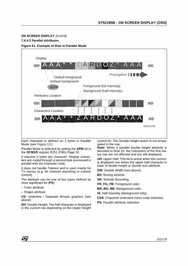
101/178
ST92185B - ON SCREEN DISPLAY (OSD)
ON SCREEN DISPLAY (Cont’d)
7.4.4.3 Parallel Attributes
Figure 61. Example of Row in Parallel Mode
Each character is defined on 2 bytes in ParallelMode (see Figure 13.)
Parallel Mode is selected by setting the SPM bit inthe DCM1R register R251 (FBh) Page 32.
It requires 2 bytes per character. Display charac-ters are coded through a second byte processed inparallel with the character code.
It does not handle Teletext and is used mainly forTV menus (e.g. for channel searching or volumecontrol).
The attribute can be one of two types defined bymost significant bit (PS):
– Color attribute
– Shape attribute
US: Underline / Separate Mosaic graphics (seeabove).
DH: Double Height: The half character is displayedin the current row depending on the Upper Height
control bit. The Double Height action is not propa-gated in the row.Note: When a parallel double height attribute isdecoded in Row 23, the characters of the first sta-tus row are not affected and are still displayed.
UH: Upper Half. This bit is active when the current-ly displayed row writes the upper half-character incase of double height or double size attribute.
DW: Double Width (see above).
BX: Boxing window.
SR: Smooth Rounding.
FR, FG, FB: Foreground color.
BR, BG, BB: Background color.
HI: Half Intensity (background only).
CSS: Character extended menu code selection.
PS: Parallel attribute selection
A R D O ZZA AA A AA * * *
Background (half intensity)
Foreground (full intensity)
Characters Location
Display
PropagationDefault foreground
Default background
global
Attributes Location
A R D O ZZA AA A AA * * *VR02115D

102/178
ST92185B - ON SCREEN DISPLAY (OSD)
ON SCREEN DISPLAY (Cont’d)Table 18. Parallel Color and Shape Attributes.
Double Size: (available in Parallel mode or in Line mode) by setting Double Width plus Double Height at-tributes.
Figure 62. Parallel Color and Shape Attributes
BIT NAME FUNCTION REMARKS0 BR Background Red
1 BG Background Green
2 BB Background Blue
3 HI Half-Intensity Only for Background.
4 FR Foreground Red
5 FG Foreground Green
6 FB Foreground Blue
7 PS= 0 Parallel Attribute Selection Color mode of parallel attributes
0 CSS Character set selectionG2-Menu characters or G1/Extended menu charac-ters selection
1 US Underline/Seperated mosaic Dual function depending on character code
2 DH Double height The character is 20 pixels high .
3 DW Double width
The character is 20 pixels wide. Available in Parallel mode or in Line mode. Characters are stretched hor-izontally, to occupy in addition, the next character space. It is possible to mix it with double height. To display a double width character the attribute must be “double width” on the character and “simple width” on the next which can be a serial attribute. In this case the first character is memorised. If two “double width” attributes are on two adjacent characters, the first half of the second is displayed instead of the second half of the first one.
4 UH Upper half character (if 1) Active only if Double Height or Size requested
5 BX Box mode Boxing window created (if 1)
6 SR Smooth rounding Special rounding effect (See Figure 5)
7 PS= 1 Parallel Attribute Selection Shape mode of parallel attributes
Characterlocation
Attributelocation
A
31
B
4F
A B A B
A
31
B
88 80
DW SS
VR02115E

103/178
ST92185B - ON SCREEN DISPLAY (OSD)
ON SCREEN DISPLAY (Cont’d)
7.4.4.4 Font Selection using Parallel Attributes
Parallel attributes have an immediate effect. Theyare applied to the associated character. These at-tributes can also have a “serial” effect, the definedattribute being still defined on the following charac-ters: this is known as attribute propagation.
Shape attributes (US,DH,BX,SR) are propagatedwhen PS is toggled to 0. In the same way, color at-tributes are propagated when PS is toggled to 1.
CSS has two kinds of behaviour:
– If PS is set once, the CSS attribute is applied on the current character only.
– If PS is set twice, the CSS of the first character with PS=1 is propagated.
Note: The value stored as a preceding CSS valueis forced when alpha or mosaic color serial at-tributes are used. Alpha serial attributes reset thememorized CSS: Mosaic serial attributes set thememorized CSS.
Table 19. Font Selection using Parallel Attributes
In the example in Table 6,, a string of six charac-ters is displayed. In the line “Display with” we cansee that, starting from Char(n) and ending withChar n+2, the CSS setting made at Char (n-2) ispropagated.
Table 20. Example of Character Set Selection
Parallel
Attribute Character Code
Character
Definition
PS= 0
00..1F 32 Control Characters (serial attributes function table)
20..7F 96 Basic Characters chosen from G0 or G1 font
80..FF 128 extended characters G2-based X/26 and Menu Characters
PS= 1
CSS used for character set selection
00..1F 32 Control Characters (serial attributes function table)
20..7FCSS= 0: G0 or G1 selection depending on color serial attribute CSS= 1: G1 selection
80..FFCSS= 0: Select G2-based X/26 + Menu CSS= 1: Select extended Menu + 32 reserved characters
Char(n-2) Char(n-1) Char(n) Char(n+1) Char(n+2) Char(n+3)PS= 1 1 0 0 1 1
CSS= CSSn-2 CSSn-1 none none CSSn+2 CSSn+3
Display with CSSn-2 CSSn-1 CSSn-2 CSSn-2 CSSn+2 CSSn+3
Stored CSS CSSn-2 CSSn-2 CSSn-2 CSSn-2 CSSn-2 CSSn+2

104/178
ST92185B - ON SCREEN DISPLAY (OSD)
ON SCREEN DISPLAY (Cont’d)
Figure 63. Parallel Mode Display Example 1 Showing Character and Attribute Byte Pairs:
Parallel Mode Display Example 2:
RAM content in Parallel Mode
A A SA B
A NF BI
A
Characters
X
SS : Simple Size b7 = 0
DW : Double Width b7 = 1
A
A
DS : Double Size b7 = 1
NC : New Colour b7 = 0
ANF
I
I
A
A
DW
DW
NC
Parallel Attribute
SS
SS
NC
DW
SS
SSSS
UH=1
DS
UH=0
NCDH
UH=1
DH
UH=0 NCNF
NFA
A
Display
A AA A A B A
A
A
A
DSNC
NC
NC
NC
NF : New Foreground (Serial Attribute)
SA : Serial Attribute
DH
UH=1
DH
UH =0
VR02112F
eM n us s 1T r e b l e
B a

105/178
ST92185B - ON SCREEN DISPLAY (OSD)
ON SCREEN DISPLAY (Cont’d)
7.4.4.5 Rules When Using Size Attributes
Secondary effects can be generated when theshape format is not respected.
The 3 figures below describe the combination ofparallel size attributes to obtain the different char-acter sizes:
· Double Width
· Double Height
· Double Size
7.4.4.6 Example of using Double WidthAttribute
In parallel mode, double width on character can beobtained using the following rule (Figure 16):
It is important to set Double Width (bit 3 of theshape attribute) on the current character attributeand Single Size on the following one. The secondcharacter location can be either a serial attribute oranother character.
On the contrary, if a new color or a Double Widthattribute is set in the second attribute location, thesecond part of the character is overlapped.
Figure 64. Double Width Examples
Attributeslocation
Characterslocation
Double widthA
New foreground(serial attribute)
NFA
SSDW
Simple sizeDouble width
1 ROW
Double widthA B
A
NCDW
New colorDouble width
New foreground(parallel attribute)
1 ROW
B
first half of the second character is displayed
VR02115G

106/178
ST92185B - ON SCREEN DISPLAY (OSD)
ON SCREEN DISPLAY (Cont’d)
7.4.4.7 Example of using Double HeightAttribute
In parallel mode, Double Height characters can beobtained as follows. The Double Height attributeconcerns two consecutive rows. Repeat the char-
acter to magnify in the two rows. Set Bit 2 DH ofthe shape attribute in the two locations and set orreset bit 4 UH to define if it is the top or bottomhalf-character.
Figure 65. Double Height Example
VR02115H
Display
New color
2 ROWS
Double heightupper half
DHUH=1DHUH=0
Attributslocation
Characterslocation
A
B
B
Double heightlower half
Double height
AShape Propagation with colorB
Previous/default color
A

107/178
ST92185B - ON SCREEN DISPLAY (OSD)
ON SCREEN DISPLAY (Cont’d)
7.4.4.8 Example of using Double Size Attribute
In parallel mode, Double Size characters can beobtained as follows. This attribute concerns twoconsecutive rows. The character to magnify must
be repeated on the two rows. Bits 2 and 3 of theshape attribute must be set on the two locations. Inaddition bit 4 must be set or reset to define the topor bottom half-character.
Figure 66. Double Size Examples
Display
Attributelocation
Characterlocation
Double size
Double Height
2 ROWS
Double size upper half
DHDSUH=1
DHDSUH=0
Double sizelower half
A
ANF
NF
A
Double Height
VR02115J

108/178
ST92185B - ON SCREEN DISPLAY (OSD)
ON SCREEN DISPLAY (Cont’d)
7.4.4.9 Example of using Underline Attribute
In parallel mode, the Underline mode on charactercan be obtained simply by setting the bit 1 ‘US’ ofthe shape attribute. To underline double height
characters, set the US bit on the attribute associat-ed with the lower part of the character.
The underline attribute is ignored in the upper half-character.
Figure 67. Underline Example
Double height
2 ROWS
DHUH=1DHUH=0
Display
Attributelocation
Characterlocation
U
U
L
L
UL
DHUH=1DHUH=0
Underline (US=1)
VR02115K
Underline (US=1)

109/178
ST92185B - ON SCREEN DISPLAY (OSD)
ON SCREEN DISPLAY (Cont’d)
7.4.4.10 Attribute Rules
The default colors for foreground and backgroundare defined through the register DCR R240 (F0h)Page 33.
A display defined in parallel mode can accept a se-rial color attribute, and propagation is available un-til a new color attribute (serial or parallel) is en-countered. Rule for Shape Attributes:
– In parallel mode, shape attributes are notpropagated on the following characters of therow except if this character has a colour at-tribute. The propagation lasts as long as a co-lour attribute is applied to a character.
– In parallel mode, the double height (bit 2 of theshape attribute) is active only on its own char-acter. Setting one double height attribute does
not cover the following characters of the row(different from double height in serial mode).
Figure 68. Rule for Serial and Parallel ColorCombination
Highest priority
defined in TDSRAM
defined in TDSRAM
defined in page register
Lowest priority
PARALLEL COLOR
SERIAL COLOR
DEFAULT COLOR

110/178
ST92185B - ON SCREEN DISPLAY (OSD)
ON SCREEN DISPLAY (Cont’d)
7.4.4.11 Cursor Control Horizontal position (by character) Vertical position (by row) Color or Underline Cursor Modes Color Cursor with inverted foreground / inverted
background Flash or Steady mode Color Cursor
Cursor display is controlled using two registers:
– Cursor Horizontal Position R246 (F6h) Page 32
– Cursor Vertical Position R247 (F7h) Page 32.
Notes:
1. Cursor operation in “Underline” mode: anyscreen location where the foreground color isidentical to the background color behaves as a“lost cursor” (i.e. cursor not visible). Assuming aserial mode display, the screen location placedon the lower row after a double height characterwill lead to a “lost cursor”.
2. Ghost fringing: assuming a cursor operation incolor inversion mode, assuming a serial modedisplay, assuming the fringe is activated, thescreen location placed on the lower row after adouble height character may show a “ghostfringing” effect (the ghost color being aninverted background one).
3. Static or flash cursor Mode: the horizontal cur-sor value indicates the character position (i.e.first character pointed with a “1” value); inUnderline Mode, the horizontal cursor valuegives the position minus “1”.
7.4.5 Vertical Scrolling Control Top-Down or Bottom-Up shift Freeze Display function Shift speed control Double Height Display scrolling
Scrolling is performed in a programmable rollingwindow if the characters are in normal height.
In Line mode, the scrolling window must be entire-ly filled by programmed rows (each scrolled loca-tion is defined by one of the 11 available rows).
Notes:
1. 80-characters combined with scrolling can onlybe used in Line mode
2. In Parallel (Level 1+) mode, scrolling is possiblewithout serial attributes DS and DH.
Use these two registers to control scrolling:
– Scrolling Control Low R248 (F8h) Page 32
– Scrolling Control High R249 (F9h) Page 32
7.4.5.1 RGB & FB DAC and TSLU OutputsThe R, G, B and FB pins of the ST92195/ST92R195 are analog outputs controlled by trueDigital to Analog Converters. These outputs arespecially designed to directly drive the Video Pro-cessor.
The R, G and B outputs are referred to Groundand they can drive up to 1.0V; they are loaded on-chip by a 0.5K ohms typical load.
The effective DAC output level is controlled by a 3bit digital code issued by the display control logicwith respect to the real time value of R, G or B andthe Half-Intensity control bit, as follows:
The FB (fast switch) output is also referred toGround and can drive up to 3.0V with an on-chip0.5K ohm load. This analog FB output provides thebest phase matching with the R, G, B signals.
An example of the Fast Blanking Signal is shownin Figure 6.
The TLSU pin is a digital output (0-5V).
R/G/B DAC code Display aspect during FB0 0 0 No Color
0 1 1 Half-Intensity Color
1 1 1 Full-Intensity Color

111/178
ST92185B - ON SCREEN DISPLAY (OSD)
ON SCREEN DISPLAY (Cont’d)
7.4.6 Display Memory Mapping Examples
The display content is stored in TDSRAM, (2 to 8Kbytes starting at address 8000h). Use registerTDPR R252 (FCh) Page 32 to address the memo-ry blocks containing the display data. Two 4-bit ad-dress pointers (bits PG and HS) must be given thatpoint to separate blocks containing the displaypage and the header/status rows.
Alternatively, the PG and HS pointers can be writ-ten to the TDPPR R246 Page 33 and TDHSPRR247 Page 33 registers.
7.4.6.1 Building a Serial Mode Full Page 40-Char Display
Page Location:
The 1 Kbyte block of page content is stored in theTDSRAM location pointed to by the PG3..PG0bits.
Header & Status Rows Location:The 0.5 Kbyte block containing the Header, StatusRow 0 and Status Row 1 is pointed to by theHS3..HS0 bits.
Row Scrolling Buffer Location:
The scrolling buffer corresponds to the 40 bytesfollowing the Row 23 when the scrolling feature isused.
Figure 69. Serial Mode (40 Characters) - Page Mapping
Figure 70. Serial Mode (40 Characters) - Header and Status Mapping
1K TDSRAM
Row 1
Row 23
Scrolling Buffer
Free Space
Resolution 1K bytes
BlockNumber(1K)
TDSRAMAddress (hex)
TDPRValue (hex)PG3..PG0
0 8000 0
1 8400 2
2 8800 4
3 8C00 6
4 9000 8
5 9400 A
6 9800 C
7 9C00 E
6K
2K
8K
0.5K TDSRAM
Header
Status Row 0
Free Space
Resolution 0.5K bytes
Block Number (0.5K)
TDSRAM Address (hex.)
TDPR Value (Hex.) HS3..HS0
0 8000 01 8200 12 8400 23 8600 34 8800 45 8A00 56 8C00 67 8E00 78 9000 89 9200 910 9400 A11 9600 B12 9800 C13 9A00 D14 9C00 E15 9E00 F
Status Row 1 6K
2K
8K

112/178
ST92185B - ON SCREEN DISPLAY (OSD)
ON SCREEN DISPLAY (Cont’d)
7.4.6.2 Building a Parallel Mode, 40-Char, FullPage Display
Page Location:The pair of adjacent 1 Kbyte blocks of page con-tent is stored in the TDSRAM location pointed toby the PG3..PG0 bits. The first block contains thecharacters, the second block contains the attributebytes.
Header & Status Rows Location:
The 0.5 Kbyte block containing the Header, StatusRow 0 and Status Row 1 is pointed to by theHS3..HS0 bits. The Header/Status attributes arestored in this block at offset 80h.
Row Scrolling Buffer Location:
The scrolling buffer corresponds to the 40 bytesfollowing Row 23 when the scrolling feature isused.
Figure 71. Parallel Mode (40 Characters) - Page Mapping
Figure 72. Parallel Mode (40 Characters) - Header and Status Mapping
1K TDSRAM
Row 1 Char.
Row 23 Char.
Scrolling Buffer
Free Space
Resolution 2K bytes
BlockNumber
(2K)
TDSRAMAddress (hex)
Char.
TDSRAMAddress (hex)
Attr.
TDPRValue (hex)PG3..PG0
0 8000 8400 0
1 8800 8C00 4
2 9000 9400 8
3 9800 9C00 C
1K TDSRAM
Row 1 Attr.
Row 23 Attr.
Scrolling Buffer
Free Space
6K
2K
8K
BlockNumber (0.5K)
TDSRAMAddress (hex)
TDPRValue (hex)HS3..HS0
0 8000 01 8200 12 8400 23 8600 34 8800 45 8A00 56 8C00 67 8E00 78 9000 89 9200 910 9400 A11 9600 B12 9800 C13 9A00 D14 9C00 E15 9E00 F
0.5K TDSRAM
Header Char.
Resolution 0.5K bytes
Status Row 0 Char.
Status Row 1 Char.
Free Space
Header Attr.
Status Row 0 Attr.
Status Row 1 Attr.
Free Space
80h
6K
2K
8K

113/178
ST92185B - ON SCREEN DISPLAY (OSD)
ON SCREEN DISPLAY (Cont’d)
7.4.6.3 Building a Serial Mode, 40-Char, LineMode Display
Half-Page Location:The 0.5 Kbyte block of half-page content is storedin the TDSRAM location pointed to by thePG3..PG0 bits.
Header & Status Rows Location:
The 0.5 Kbyte block containing the Header, StatusRow 0 and Status Row 1 is pointed to by theHS3..HS0 bits. The Row attribute (row count) isstored in this block at offset 100h and contains 12bytes for line mode (see DCM1R register descrip-tion).
Row Scrolling Buffer Location:The scrolling buffer corresponds to Row 12 whenthe scrolling feature is used (in this case 11 rowsare scrolled).
Figure 73. Serial (40 Characters) Line Mode Mapping
0.5K TDSRAM
Row 1
Row 11
Row 12/ Scrolling Buffer
Free Space
Resolution 0.5K bytes
See Figure 22 for Address Values
0.5K TDSRAM
Header Char.
Resolution 0.5K bytes
Status Row 0
Status Row 1
Free Space
Row Attr.
Free Space
100h
Block Number (0.5K)
TDSRAM Address
(hex.)
TDPR Value (Hex.)
PG3..PG00 8000 01 8200 12 8400 23 8600 34 8800 45 8A00 56 8C00 67 8E00 78 9000 89 9200 910 9400 A11 9600 B12 9800 C13 9A00 D14 9C00 E15 9E00 F
6K
2K
8K

114/178
ST92185B - ON SCREEN DISPLAY (OSD)
ON SCREEN DISPLAY (Cont’d)
7.4.6.4 Building a Parallel Mode, 40 Char, Linemode Display
Half-Page Location:The pair of adjacent 0.5 Kbyte blocks of half pagecontent is stored in the TDSRAM location pointedto by the PG3..PG0 bits. One block contains thecharacters, the other block contains the attributebytes.
Header & Status Rows Location:
The 0.5 Kbyte block containing the Header, StatusRow 0 and Status Row 1 is pointed to by theHS3..HS0 bits.
The Header/Status attributes are stored in thisblock at offset 80h.
The Row attribute (row count) is stored in thisblock at offset 100h and contains 12 bytes for linemode (see DCM1R register description).
Row Scrolling Buffer Location:The scrolling buffer corresponds to the Row 12when the scrolling feature is used (in this case 11rows are scrolled).
Figure 74. Parallel (40 Characters) Line Mode Mapping
See Figure 22 for Address Values
Resolution 1K bytes
See Figure 21 for Address Values
0.5K TDSRAM
Header Char.
Resolution 0.5K bytes
Status Row 0
Status Row 1
Free Space
Header Attr.
Status Row 0
Status Row 1
Free Space
Free Space
Row Attr.
80h
100h
0.5K TDSRAM 0.5K TDSRAM
Row 1 Attr.
Row 11 Attr.
Free Space
Row 12/Scrolling Buffer
Row 1 Char.
Row 11 Char.
Free Space
Row 12/Scrolling Buffer

115/178
ST92185B - ON SCREEN DISPLAY (OSD)
ON SCREEN DISPLAY (Cont’d)
7.4.6.5 Building a Serial Mode, 80 Char, FullPage Display
Half-Page Location:The pair of adjacent 1 Kbyte blocks of page con-tent is stored in the TDSRAM location pointed toby the PG3..PG0 bits. The first block contains theleft side of the page, the second block contains theright side of the page.
Header & Status Rows Location:
The 0.5 Kbyte block containing the Header, StatusRow 0 and Status Row 1 is pointed to by theHS3..HS0 bits.
Row Scrolling Buffer Location:The scrolling buffer corresponds to the 40 bytesfollowing the Row 23 when the scrolling feature isused.
Figure 75. Serial Mode (80 Characters) - Page Mapping
See Figure 22 for Address Values
1K TDSRAM
Row 1 Left
Row 23
Resolution 2K bytes
1K TDSRAM
Row 1 Right
See Figure 23 for Address Values
Row 23
0.5K TDSRAM
Header
Resolution 0.5K bytes
Status Row 0
Status Row 1
Free Space
Free Space Free Space
Scrolling Buffer Scrolling Buffer

116/178
ST92185B - ON SCREEN DISPLAY (OSD)
ON SCREEN DISPLAY (Cont’d)
7.4.6.6 Building a Serial Mode, 80 Char, LineMode Display
Half-Page Location:The pair of 0.5 Kbyte blocks of half page content isstored in the TDSRAM location pointed to by thePG3..PG0 bits. The first block contains the left halfrows, the other block contains the right half rows.
Header/Status Rows Location:
The 0.5 Kbyte block containing the Header, StatusRow 0 and Status Row 1 is pointed to by theHS3..HS0 bits.
The Row attribute (row count) is stored in thisblock at offset 100h and contains 12 bytes for linemode (see DCM1R register description).
Row Scrolling Buffer Location:
The scrolling buffer corresponds to Row 12 whenthe scrolling feature is used (in this case 11 rowsare scrolled).
Figure 76. Serial (80 Characters) Line Mode Mapping
Figure 77. Serial (80 Characters) Line Mode - Header and Status Mapping
0.5K TDSRAM
Resolution 1K bytes
BlockNumber(1K)
TDSRAMAddress Left
(hex)
TDSRAMAddress Right
(hex)
TDPRValue (hex)PG3..PG0
0 8000 8200 0
1 8400 8600 2
2 8800 8A00 4
3 8C00 8E00 6
4 9000 9200 8
5 9400 9600 A
6 9800 9A00 C
7 9C00 9E00 E
Row 1 Left
Row 11
Free Space
Row 12/Scroll Buffer
0.5K TDSRAM
Row 1 Right
Row 11
Free Space
Row 12/Scroll Buffer
6K
2K
8K
See Figure 22 for Address Values
0.5K TDSRAM
Header
Resolution 0.5K bytes
Status Row 0
Status Row 1
Free Space
Free Space
Row Attr.
100h

117/178
ST92185B - ON SCREEN DISPLAY (OSD)
ON SCREEN DISPLAY (Cont’d)
7.4.7 Font Mapping
G0 is the basic character font.
G1 is the mosaic font. It is not stored in ROM but isimplemented in hardware. In serial mode it is ad-dressed by a serial attribute (See Figure 3). In par-allel mode it is accessed by bit 0 (CSS) of the par-allel shape attribute and bit 1 (US) for separatedmosaic (See Figure 4).
G2 is a font of X/26 based + Menu shared charac-ters.
An Extended Menu character font available in par-allel mode. It is accessed via bit 0 (CSS) in the par-allel shape attribute (Character Set Selection).The Extended Menu font is not accessible in serialmode.
7.4.8 Font Mapping Modes
There are two font mapping modes selected
by the NCM bit in the NCSR register R245 (F5h)Page 32:
Single G0 mode
A set combining 83 characters fromthe G0 basic set plus 13 charactersselected from 15 National charactersubsets. The National character sub-sets are selected by four bits (NC3:0)in the NCSR register R245 (F5h)Page 32.
Triple G0 mode
Three 96-character character sets(G0-0, G0-1 and G0-2) for multi al-phabet applications. Character setselection is done by four bits (NC1:0or NC3:2) in the NCSR register R245(F5h) Page 32.
– In Serial Mode (Level 1), only 256 Character Codes are available using an 8-bit code. The character codes plus some serial attributes and some additional programmable options address 566 chars: 256 + 182 NS chars + 128 mosaics in single G0 mode.
– In Parallel Mode (Enhanced Level 1), 512 Char-acter Codes are available using a 9-bit code. The character codes plus some serial and parallel at-tributes, and some additional programmable op-tions address 662 chars: 256 + 182 NS chars + 128 mosaic + 96 extended chars. in single G0 mode.
Display ROM Font Entry:The user must define his own fonts for:
– 278 characters: - 15 x 13 G0 National Character subsets + 83 G0 Character set
or
– 288 characters: 3 x 96-character character sets
– 128 G2 based X/26 and Menu characters
– 96 Extended Menu characters
Table 21. Triple G0 Mode - Font Mapping
ROM Address
CharacterCode
CSS Font Usage
000h to 01Fh 0E0h to 0FFh 1 Extended menu
020h to 07Fh 020h to 07Fh0
(or serial mode)
G0 set 0
080h to 0FFh 080h to 0FFh G2 + Menu
100h to 15Fh 020h to 07Fh G0 set 1
160h to 1BFh 020h to 07Fh G0 set 2
1C0h to 1FFh 0A0h to 0DFh 1 Extended menu

118/178
ST92185B - ON SCREEN DISPLAY (OSD)
ON SCREEN DISPLAY (Cont’d)
Table 22. National Character Subset Mapping(Ordered by their G0 address)
Figure 78. Font Mapping
1st 2nd 3rd 4th 5th 6th 7th
23h 24h 40h 5Bh 5Ch 5Dh 5Eh
8th 9th 10th 11th 12th 13th
5Fh 60h 7Bh 7Ch 7Dh 7Eh
PARALLEL MODE(PS=x, CSS=0)
SERIAL
ATTRIBUTES
(32 CODES)
G2 BASED
+ MENU
(128 CODES)
G0 + OPTIONAL NATIONAL SET
80 FF
Addresses
Char. Codes
(96 CODES)
0 1F 7F
0 1F 7F 80 FF
SERIAL
ATTRIBUTES
(32 CODES)
G2 BASED
+ MENU
(128 CODES)
G0 + OPTIONAL NATIONAL SET
80 FF
SERIAL MODE
Addresses
Char. Codes
(96 CODES)
G1* (32) G1* (32)
*If Serial Attributes 19, 1A are used
0 1F 3F 5F 7F
0 1F 7F 80 FF
SERIAL
ATTRIBUTES
(32 CODES)
EXTENDED
MENU CHARACTERS
(96 CODES)
80 FF
Addresses
Char. Codes
G1 (32) G1 (32)
0 1F 3F 5F 7F
100 11F 17F 19F 1FF
PARALLEL MODE(PS=1, CSS=1)
G0 (32) RESERVED (32)
180
9F

119/178
ST92185B - ON SCREEN DISPLAY (OSD)
ON SCREEN DISPLAY (Cont’d)Table 23. Single G0 Mode - Font Mapping
Table 24. National Character Subsets
ROM Address Character Code CSS Font Usage NC(3:0)000h to 01Fh 0E0h to 0FFh 1 Extended menu
020h to 07Fh 020h to 07Fh
0
G0 + National Character Subset 0 (96 chars) 0000b
080h to 0FFh 080h to 0FFh G2 + Menu (128 chars)
100h to 10Ch (see table below) National Character Subset 1 (13 chars) 0001b
10Dh to 119h (see table below) National Character Subset 2 (13 chars) 0010b
11Ah to 126h (see table below) National Character Subset 3 (13 chars) 0011b
127h to 133h (see table below) National Character Subset 4 (13 chars) 0100b
134h to 140h (see table below) National Character Subset 5 (13 chars) 0101b
141h to 14Dh (see table below) National Character Subset 6 (13 chars) 0110b
14Eh to 15Ah (see table below) National Character Subset 7 (13 chars) 0111b
15Bh to 167h (see table below) National Character Subset 8 (13 chars) 1000b
168h to 174h (see table below) National Character Subset 9 (13 chars) 1001b
175h to 181h (see table below) National Character Subset 10 (13 chars) 1010b
182h to 18Eh (see table below) National Character Subset 11 (13 chars) 1011b
18Fh to 19Bh (see table below) National Character Subset 12 (13 chars) 1100b
19Ch to 1A8h (see table below) National Character Subset 13 (13 chars)(Free for user) 1101b
1A9h to 1B5h (see table below) National Character Subset 14 (13 chars) (Menu chars.) 1110b
1C0h to 1FFh 0A0h to 0DFh 1 Extended menu
23 5C5B4024 5D 5E 5F 60 7B 7C 7D 7E
Estonian 9
Czech/Slovak 3
English 0
French 1
German 4
Italian 6
Lettish/ 10
Polish 8
Portugese/ 5
Rumanian 7
Serbian/ 12
Swedish/ 2
Turkish 11
Lithuanian
Spanish
Croatian/Slovenian
Finnish
Subset No. Character Code (Hex)Subset Name (Decimal)

120/178
ST92185B - ON SCREEN DISPLAY (OSD)
ON SCREEN DISPLAY (Cont’d)
Figure 79. Pan-European Font (East/West) Character Codes (Hex.)
Figure 80. OSD Picture in Parallel Mode
National Character Subset 0
Menu
G0_0
G2-Menu
Extended
MenuExtended
Char.National
Subsets1..14d

121/178
ST92185B - ON SCREEN DISPLAY (OSD)
ON SCREEN DISPLAY(Cont’d)
7.4.9 Register Description
HORIZONTAL BLANK REGISTER (HBLANKR)R240 - Read/WriteRegister Page: 32Reset Value: 0000 0011 (03h)
It controls the length of the Horizontal Blank whichfollows the horizontal sync pulse.
Bit 7:0 = HB[7:0]: The horizontal blank period iscalculated with a pixel down counter loaded oneach Hsync by HB[7:0]. During this period, FB = 0and (R, G, B) = black.
Thblank = [(HB7*128 + HB6*64 + HB5*32 +HB4*16 + HB3*8 + HB2*4 + HB1*2 + HB0) * Tpix]
HORIZONTAL POSITION REGISTER (HPOSR)R241 - Read/WriteRegister Page: 32Reset Value: 0000 0011 (03h)
Bit 7:0 = HP[7:0]: The horizontal start position iscalculated with a pixel down-counter loaded oneach Hsync by HP[7:0]. The first character displaystarts when the counter turns to zero.
Hori delay= [(HP7*128 + HP6*64 + HP5*32 +HP4*16 + HP3*8 + HP2*4 + HP1*2 + HP0) * Tpix]+ Thblank
VERTICAL POSITION REGISTER (VPOSR)R242 - Read/WriteRegister Page: 32Reset Value: 0000 0000 (00h)
Bit 7:6 = Reserved, keep in reset state.
Bit 5:0 = VP[5:0]: The vertical start position is cal-culated with a line downcounter decremented oneach Hsync by VP[5:0]. The Display of the first rowbegins when the counter turns to zero.
Vert delay = (VP5*32 + VP4*16 + VP3*8 + VP2*4+ VP1*2 + VP0) * Tline (Tline= 64 µs)
7 0
HB7 HB6 HB5 HB4 HB3 HB2 HB1 HB0
7 0
HP7 HP6 HP5 HP4 HP3 HP2 HP1 HP0
7 0
0 0 VP5 VP4 VP3 VP2 VP1 VP0

122/178
ST92185B - ON SCREEN DISPLAY (OSD)
ON SCREEN DISPLAY (Cont’d)
FULL SCREEN COLOR CONTROL REGISTER(FSCCR)R243 - Read/WriteRegister Page: 32Reset Value: 0000 0000 (00h)
Bit 7 = BE: Box Enable, see Table 11.
Bit 6 = TIO: Text out/not in, see Table 11.
Bit 5 = MM: Mixed Mode, see Table 11.
Note: When Flash and Box attributes are decodedat the same time on the characters of a header(when BE=1, MM=1, TIO=1) the full screen overthe characters is displayed as transparant.
Bit 4 = HTC: Half-Tone/Translucency Control BitThis bit allows the selection of TSLU or HT as al-ternate function output.0: TSLU is selected as I/O pin alternate function1: HT is selected as I/O pin alternate function
Bit 3:0 = FSC[3:0]: Full Screen Color control bits:FSC[3:0]= (Half-intensity, R, G, B)
Table of Color Values (hex)
Table 25. Box Mode/Translucency Configurations
7 0
BE TIO MM HTC FSC3 FSC2 FSC1 FSC0
0 Black 8 Black
1 Blue 9 Dark blue
2 Green A Dark green
3 Cyan B Dark cyan
4 Red C Dark red
5 Magenta D Dark magenta
6 Yellow E Dark yellow
7 White F Grey
BE TIO MM If Translucency is not used If Translucency is used0 x 0 Solid Background for all the display Translucent Background for all the display
0 x 1 Transparent Background for all the display Transparent Background for all the display
1 0 0 Text inside box solid, Text outside box blankedText inside box translucent, Text outside box blanked
1 0 1Text inside box with solid background Text out-side box with transparent background
Text inside box with translucent background Text outside box with transparent background
1 1 0Text inside box not displayed, transparent back-ground. Text outside box with solid background
Text inside box not displayed, transparent back-ground. Text outside box with translucent back-ground
1 1 1Text inside box with transparent background. Text outside box with solid background
Text inside box with transparent background. Text outside box with translucent background
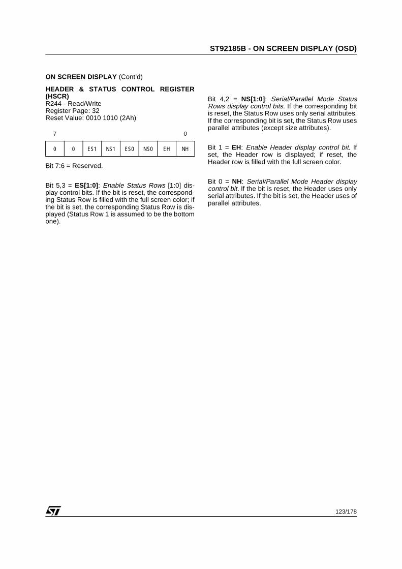
123/178
ST92185B - ON SCREEN DISPLAY (OSD)
ON SCREEN DISPLAY (Cont’d)
HEADER & STATUS CONTROL REGISTER(HSCR)R244 - Read/WriteRegister Page: 32Reset Value: 0010 1010 (2Ah)
Bit 7:6 = Reserved.
Bit 5,3 = ES[1:0]: Enable Status Rows [1:0] dis-play control bits. If the bit is reset, the correspond-ing Status Row is filled with the full screen color; ifthe bit is set, the corresponding Status Row is dis-played (Status Row 1 is assumed to be the bottomone).
Bit 4,2 = NS[1:0]: Serial/Parallel Mode StatusRows display control bits. If the corresponding bitis reset, the Status Row uses only serial attributes.If the corresponding bit is set, the Status Row usesparallel attributes (except size attributes).
Bit 1 = EH: Enable Header display control bit. Ifset, the Header row is displayed; if reset, theHeader row is filled with the full screen color.
Bit 0 = NH: Serial/Parallel Mode Header displaycontrol bit. If the bit is reset, the Header uses onlyserial attributes. If the bit is set, the Header uses ofparallel attributes.
7 0
0 0 ES1 NS1 ES0 NS0 EH NH

124/178
ST92185B - ON SCREEN DISPLAY (OSD)
ON SCREEN DISPLAY (Cont’d)
NATIONAL CHARACTER SET REGISTER (NCSR)R245 - Read/WriteRegister Page: 32Reset Value: 0000 0000 (00h)
The register bit values are sampled and then acti-vated only at each field start (on Vsync pulse).
Bit 7 = TSLE: Translucency/Half-Tone Output En-able bit.0: Translucency/Half-Tone signal disabled1: Translucency/Half-Tone is enabled. Translu-
cency or Half-Tone realtime control signal is routed in the TSLU/HT pin (depending on the HTC bit in the FSCCR register).
Note: Translucent display depends also on theBE, TIO and MM bits, see Table 11.
Bit 6 = Reserved.
Bit 5 = SWE: G0 Switch Enable Control Bit.In case of a multiple G0 alphabet configuration(NCM=1), this bit allows to switch from a first to asecond predefined G0 alphabet, using a single se-rial attribute (1Bh). In case of a single G0 alphabetconfiguration (NCM=0), the SWE bit will have noeffect.
If SWE is reset, the used G0 alphabet is pointedthrough NC[1:0].
If SWE is set, the used G0 alphabet is pointedthrough NC[3:2] and NC[1:0] toggled by 1Bh serialattribute.
Bit 4 = NCM: National Character Mode control bit.This bit reconfigures a part of the font set as defin-ing:
– either a single G0 alphabet with up to 15 national sub-sets,
– or 3 different G0 alphabets.
If NCM is reset, a single G0 alphabet configurationis activated and the 15 national sub-sets are se-lected through the NC[3:0] bits.
If NCM is set, a triple G0 alphabet configuration isactivated, the selection of the G0 set used for thedisplay is done through either NC[3:2] or NC[1:0]bits, depending upon the SWE control bit and theserial attribute 1Bh values.
Bit 3:0 = NC[3:0]: National Character Set Selec-tion.If the NCM bit is reset, these bits define which na-tional sub-set has to be used to complete the basiccurrently used G0 alphabet set.
If the NCM is set, these bits define which G0 isused.
Figure 81. National Characters Selection
7 0
TSLE 0 SWE NCM NC3 NC2 NC1 NC0
NCM
SWENC[3:0]
G0-0G0-1G0-2
G0-0G0-1G0-2
G0-0G0-1G0-2
SERIAL ATTR. 1Bh
NC[1:0] NC[3:2]
NC[1:0] TOGGLE
NS0NS1
NS14
15 NATIONALCHAR. SETS
3 G0 SETS
0
0 1
1

125/178
ST92185B - ON SCREEN DISPLAY (OSD)
ON SCREEN DISPLAY (Cont’d)
CURSOR HORIZONTAL POSITION REGISTER(CHPOSR)R246 - Read/WriteRegister Page: 32Reset Value: 0000 0000 (00h)
Bit 7 = Reserved.
Bit 6:0 = CHP[6:0]: Cursor Horizontal Position.The cursor is positioned by character.
CHP= 0 points to the first characterCHP= 39d points to the end of the row (singlepage display)CHP= 79d points to the last character in the row(double page display)
CURSOR VERTICAL POSITION REGISTER(CVPOSR)R247 - Read/WriteRegister Page: 32Reset Value: 0000 0000 (00h)
Bit 7 = FON: "Flash On" flag bit. The FON bit remains at "0" during 32 consecutive
TV fields followed by a "1" state during the 16 nextTV fields. This flag provides a 1Hz time referencefor an easy software control of all flashing effects(assuming a 50 Hz TV signal, the FON total periodwill be 0.96 seconds).
This bit is READ ONLY. Trying to write any valuewill have no effect.
Bit 6:5 = CM[1:0]: Cursor Mode control bits.
Bit 4:0 = CVP[4:0]: Cursor Vertical Position.The cursor is positioned by row. The cursor is al-ways single size.
CVP= 0 locates the cursor on the Header row
CVP= 25d locates the cursor on the last Statusrow.
7 0
0 CHP6 CHP5 CHP4 CHP3 CHP2 CHP1 CHP0
7 0
FON CM1 CM0 CVP4 CVP3 CVP2 CVP1 CVP0
CM1 CM0 Cursor Mode0 0 Cursor Disable
0 1Static Cursor (inverted foreground & invert-ed background colours)
1 0Flash Cursor (flash from current to inverted colours & vice versa)
1 1Cursor done with Underline (use of current foreground color)

126/178
ST92185B - ON SCREEN DISPLAY (OSD)
ON SCREEN DISPLAY (Cont’d)
SCROLLING CONTROL LOW REGISTER(SCLR)R248 - Read/WriteRegister Page: 32Reset Value: 0000 0000 (00h)
Bit 7 = SCE: Scrolling EnableBefore enabling scrolling, the scrolling area mustbe defined by the FRS[4:0] and LRS[4:0] bits. Thescrolling direction is defined by the UP/D bit.0: Disable scrolling1: Enable scrolling
Bit 6 = FSC: Freeze scrollingNote: The 2 control bits SCE and FSC must be setto "1" before enabling the Global double height(see the DH bit in the SCHR register).
Bit 5 = SS: Scrolling Speed Control bit.0: The display is shifted by 2 TV lines at each TV
frame (i.e. after 2 Vertical sync pulses).1: The display is shifted by 4 TV lines at each TV
frame.
Bit 4:0 = FRS[4:0]: These bits define the upper-most Row value to be scrolled (rows are num-bered from 1 to 23). In case of global double heightmode programming, FRS[4:0] must mandatorilybe equal to 00000.
Table 26. Scrolling Control Bits
7 0
SCE FSC SS FRS4 FRS3 FRS2 FRS1 FRS0
DH SCE FSC UP/D FRS[4:0] LRS[4:0] Meaning0 0 x x x x No Global Double Height, No Scrolling
0 1 x1 x x No Global Double Height, Scroll up
0 x x No Global Double Height, Scroll down
1 0 x1 0 x Global Double Height, No Scrolling, Display top half
0 0 x Global Double Height, No Scrolling, Display bottom half

127/178
ST92185B - ON SCREEN DISPLAY (OSD)
ON SCREEN DISPLAY (Cont’d)
SCROLLING CONTROL HIGH REGISTER(SCHR)R249 - Read/WriteRegister Page: 32Reset Value: 0000 0000b (00h)
Bit 7 = DH: Global Double Height control bit.This bit must only be used in Page Mode. WhenDH is set, the display is turned in double height in-cluding the header, excluding the vertical offsetbefore the display area. The status rows are notaffected by the DH bit and they remain in normalheight. Depending on the value of the UP/D con-trol bit, when DH is set, the first or second half ofthe page is displayed in double height. This bit as-sumes a zooming function.
Notes: – In global double height, when the top half page
is displayed, if row 11 has a double height at-tribute, the first status row is corrupted. To avoid this effect, save row 11, remove the serial double height attribute from this row and display the up-per part of the page. Then, before displaying the lower part of the page, restore the serial DH at-tribute in row 11.
– When the bottom half page is displayed, if row 23 has a double height attribute, the first status row is not displayed. To avoid this effect remove the serial double height attribute from row 23.
Bit 6 = EER: End of Extra Row flag bit. This bit is forced to "1" by hardware when the lastline of the extra row is displayed in case of scroll-ing in normal height. This bit is Read only.
In Global double height, the EER bit is set to "1"each time the last line of a new displayed row ap-pears.
Bit 5 = UP/D: Scrolling Up/DownThis bit has two functions: to control the scrollingdirection and to select the half part of the page inGlobal Double Height display.Scrolling direction:0: Top-Down shift1: Bottom-up shift
Half-page selection:
When DH is set, if UP/D is set, the upper half of thepage is displayed (i.e. Header and the page rows 1to 11).
When DH is set, if UP/D is reset, the lower half ofthe page is displayed (i.e. rows 12 to 23 and theStatus rows).
The UP/D control bit must be defined before set-ting the Global height (DH bit); changing UP/D af-ter DH is set, will not change the already selectedhalf page.
Bit 4:0 = LRS[4:0]: Last row to be scrolled (1 to23). In case of scrolling in global double height, theLast row must be equal to 0x 10111 to display thestatus row in the two half pages.
7 0
DH EER UP/D LRS4 LRS3 LRS2 LRS1 LRS0

128/178
ST92185B - ON SCREEN DISPLAY (OSD)
ON SCREEN DISPLAY (Cont’d)
Figure 82. Memory Management for Scrolling Window
ROW A
ROW B
ROW C
ROW A
ROW B
ROW CROW D
ROW B
ROW C
ROW D
ROW A
ROW B
ROW CROW D
ROW A
ROW B
ROW C
ROW A
ROW B
ROW CROW D
ROW A
ROW B
ROW CROW D
ROW A
ROW B
ROW CROW D
ROW A
ROW B
ROW C
ROW A
ROW B
ROW CROW D
ROW B
ROW C
ROW D
ROW B
ROW C
ROW DROW E
Normal Height
T03 rows to be
scrolled
T + 5 VSYNC
T + 10 VSYNC
T + 15 VSYNC
EER=0
EER=0
EER=1
EER=0
ROW A
ROW B
ROW C
ROW D
ROW B
ROW C
ROW D
ROW E
TDSRAMCONTENTDISPLAYAREA
Row 24
Row 24
TDSRAMCONTENT
NEW
A = First row to scrollC= Last row to scrollE= Extra row
Freeze offafter 5 Vsync
Freeze onafter 5 Vsync
New TDSRAM addressafter EER=1

129/178
ST92185B - ON SCREEN DISPLAY (OSD)
ON SCREEN DISPLAY (Cont’d)
DISPLAY CONTROL MODE 0 REGISTER(DCM0R)R250 - Read/WriteRegister Page: 32Reset Value: 0000 0000 (00h)
Bit 7 = DE: Display Enable control bit.If DE is reset, no display will be performed. If DE isset, a display will be done as defined through thevarious control bits.
Bit 6 = STE: Semi-Transparent Enable bit.This bit is active only in Single page display mode.
While the Display is disabled, the horizontal andvertical sequencers are forced in their reset stateand the RGB & FB DACs are not off (still present-ing on-chip resistors to Ground).
Note: This mode shows a visible grid on thescreen.
Bit 5 = FRE: Fringe Enable control bit. If this bit is set, and the SWE bit is reset (refer tothe National Character Set Register description)the serial attribute 1Bh has a fringe toggle func-tion.
Bit 4 = CE: Conceal Enable control bit.0: Reveal any text defined as concealed by serial
attributes (Default)
1: Conceal any text defined as concealed by serial attributes
Bit 3 = GFR: Global Fringe Enable control bit. If this bit is set, the whole display is in fringe mode(except if a Double page display mode is pro-grammed).
Bit 2 = GRE: Global Rounding Enable control bit.If this bit is set, the whole display is in roundingmode (except if a Double page display mode isprogrammed).
Bit 1 = SF: Screen Format control bit.0: Configures the Display for 4/3 TV screen format.1: A fixed offset of 128 Pixel clock periods is added
before any character is displayed; the Full Screen Color attribute is used while the offset is running.
The SF bit intended for displaying on 16/9 TVscreen format tubes, the display picture will be re-centered.
Bit 0 = S/D: Single or Double page control bit.0: A single page is displayed on screen (i.e. 40-
character width).1: A set of two pages is displayed contiguously
(i.e. 80-character width).
Note: In 80 characters per row and in full pagemode, line 25 of each field is displayed as atransparant line (as this line is not in the visiblepart of the screen, this should not present a limita-tion).
Programming a Double page display will automat-ically mask the Fringe, Rounding and ParallelMode control bits. Their register values are notchanged and they will automatically recover theirinitial effect if the display is switched back in a Sin-gle page mode.
7 0
DE STE FRE CE GFR GRE SF S/D
FRE SWE 1Bh Serial attribute acts as:0 0 No Action
0 1 G0 Toggle
1 0 Fringe Toggle
1 1 G0 Toggle

130/178
ST92185B - ON SCREEN DISPLAY (OSD)
ON SCREEN DISPLAY (Cont’d)
DISPLAY CONTROL MODE 1 REGISTER(DCM1R)R251 - Read/WriteRegister Page: 32Reset Value: 0000 0000 (00h)
Bit 7:4 = Reserved bits, keep in reset state.
Bit 3 = EXTF: External Font. Only when the emulator is used, this bit selects thefont memory containing a user-defined OSD font.In normal user application, this bit has no effect.0: Internal font memory of the emulator chip.1: External font RAM of the emulator board.
Bit 2 = FBL: Fast Blanking Active Level control bit.The FBL bit must be reset if the on-screen displayis done while the FB output is low. The FBL bitmust be set if the on-screen display is done whilethe FB output is high. This bit also controls theTSLU AF output polarity with the same rule as forFB.
Bit 1 = PM: Line Mode control bit.If PM is reset, the display is working in Full pagemode, i.e. the screen is composed of one header,23 text rows plus 2 status rows. If PM is set, thedisplay works in Line mode.
Line mode allows up to 12 rows to be displayedanywhere on the screen. The row attribute (seeTDSRAM mapping) contains the row numbers onthe screen. The byte position of the row attributeconrresponds to the row in the TDSRAM. For ex-ample, if the 3rd byte of the row attribute contains6, the 3rd row in TDSRAM will be displayed as the6th row on the screen.
Bit 0 = SPM: Serial/Parallel Mode control bit.If the SPM bit is reset, the display is done in Serial
mode, i.e. a character or attribute is coded with asingle byte. If the SPM bit is set, the display isdone in Parallel mode, i.e. a character or an at-tribute is coded on two bytes.
TDSRAM POINTER REGISTER (TDPR)R252 - Read/WriteRegister Page: 32Reset Value: 0000 0000 (00h)
Bit 7:4 = HS[3:0]: Location of the current Headerand Status Rows in the TDSRAM.
Bit 3:0 = PG[3:0]: Location of the current Pagecontent (rows 1 to 23) in the TDSRAM. For moredetails, refer to Section .
The HS[3:0] and PG[3:0] bits described by theR246 and R247 registers in page 32. Display loca-tions, Head/Stat location, Page location, are phys-ically the same: these sets of address bits can bemodified through two different programming ac-cesses.
7 0
0 0 0 0 EXTF FBL PM SPM
7 0
HS3 HS2 HS1 HS0 PG3 PG2 PG1 PG0

131/178
ST92185B - ON SCREEN DISPLAY (OSD)
ON SCREEN DISPLAY (Cont’d)
DISPLAY ENABLE 0 CONTROL REGISTER(DE0R)R253 -Read/WriteRegister Page: 32Reset Value: 1111 1111 (FFh)
Bit 7:0 = R[8:1]: Row display enable control bit.When the “Ri” bit is set (Reset value), the corre-sponding row (with row in the page, numberedfrom 1 to 23) will be displayed. When the “Ri” bit isreset, the full screen color is displayed.
DISPLAY ENABLE 1 CONTROL REGISTER(DE1R)R254 -Read/WriteRegister Page: 32Reset Value: 1111 1111 (FFh)
Bit 7:0 = R[16:9]: Row display enable control bit.When the “Ri” bit is set (Reset value), the corre-sponding row (with row in the page, numberedfrom 1 to 23) will be displayed. When the “Ri” bit isreset, the full screen color is displayed.
DISPLAY ENABLE 2 CONTROL REGISTER(DE2R)R255 -Read/WriteRegister Page: 32Reset Value: x111 1111 (xFh)
Bit 7 = Reserved
.
Bit 6:0 = R[23:17]: Row display enable control bit.When the “Ri” bit is set (Reset value), the corre-sponding row (with row in the page, numberedfrom 1 to 23) will be displayed. When the “Ri” bit isreset, the full screen color is displayed.
7 0
R8 R7 R6 R5 R4 R3 R2 R1
7 0
R16 R15 R14 R13 R12 R11 R10 R9
7 0
x R23 R22 R21 R20 R19 R18 R17

132/178
ST92185B - ON SCREEN DISPLAY (OSD)
ON SCREEN DISPLAY (Cont’d)
DEFAULT COLOR REGISTER (DCR)R240 - Read/WriteRegister Page: 33Reset Value: 0111 0000 (70h)
Bit 7:4 = DFG[3:0]: Default Foreground Color.DFG[3:0] = (Half-Intensity, R, G, B)
Bit 3:0 = DBG[3:0]: Default Background ColorDBG[3:0] = (Half-Intensity, R, G, B)
Table of Color Values (hex)
CURSOR ABSOLUTE VERTICAL POSITIONREGISTER (CAPVR)R241 - Read/WriteRegister Page: 33Reset Value: 0000 0000 (00h)
Bit 7:5 = Reserved, keep in reset state.
Bit 4:0 = ACP[4:0]: Absolute Vertical Position ofthe cursor in case of double height or scrolling.
TDSRAM PAGE POINTER REGISTER (TDPPR)R246 - Read/WriteRegister Page: 33Reset Value: xxx0 0000 (x0h)
Bit 7:4 = Reserved, keep in reset state.
Bit 3:0 = PG[3:0]: Page PointerLocation of the current Page content (rows 1 to 23)in the TDSRAM. For more details, refer to the Dis-play Memory Mapping Section .
TDSRAM HEADER/STATUS POINTER REGIS-TER (TDHSPR)R247 - Read/WriteRegister Page: 33Reset Value: xxx0 0000 (x0h)
Bit 7:4 = Reserved, keep in reset state.
Bit 3:0 = HS[3:0]: Header/Status Rows PointerLocation of the current Header and Status Rows inthe TDSRAM. For more details, refer to the Dis-play Memory Mapping paragraph Section .
7 0
DFG3 DFG2 DFG1 DFG0 DBG3 DBG2 DBG1 DBG0
0 Black 8 Black
1 Blue 9 Dark blue
2 Green A Dark green
3 Cyan B Dark cyan
4 Red C Dark red
5 Magenta D Dark magenta
6 Yellow E Dark yellow
7 White F Grey
7 0
0 0 0 ACP4 ACP3 ACP2 ACP1 ACP0
7 0
x x x 0 PG3 PG2 PG1 PG0
7 0
x x x 0 HS3 HS2 HS1 HS0

133/178
ST92185B - ON SCREEN DISPLAY (OSD)
7.4.10 Application Software Examples
Before starting an OSD Display, it is very important to start all the internal clock/timings
To understand the software routines given below, make a thorough study of the chapters on the Resetand Clock Control Unit (RCCU) and the TDSRAM Interface.
Initialization of the Internal Clock;=========================================================================
; MAIN CLOCK INIT
;=========================================================================
CLOCKS::
;--------- CPU MAIN CLOCK ------------
; C K M A I N provided by the freq. multplier
spp #TCCR_PG; Timings & clock Controller registers page
; page 39 or 27
ld MCCR,#0x05; program the frequency multiplier down
; counter in the feed-back loop (253 =FD)
; freq=(5+1)*2 =12Mhz
; freq=(7+1)*2 =16Mhz
; freq=(8+1)*2 =18Mhz
ld MCCR,#0x85; enable the freq. multiplier
srp #BK20
ldw rr0,#0x2FFF;
time_stab1: ; for frequency multiplier stabilization
decw rr0; change CPU source clock & wait clock stabilization
cpw rr0,#0x00;
jxnz time_stab1;
ld MCCR,#0xC5 ; select the freq. multiplier as main clock
pop ppr
;=========================================================================
; SYNCHRO START
;=========================================================================
spp #SYCR_PG ; set page pointer to page 23h or 35 decimal
ld CSYCTR,#000h; R243, Hsync and Vsync from deflection part (external)
ld CSYSUR,#0C4h; R242 Sync Controller Set-up register
; Standard mode, Positive polarity of Hsync & Vsync
; delay on Hsync/Vsync HSF(3:0)=9
;=========================================================================
; DISPLAY PIXEL CLOCK
;=========================================================================
;
spp #TCCR_PG; Timings & clock Controller registers page
; set page pointer to page 39 decimal
ld SKCCR, #0x09; FE, Skew clock control register
; program the frequency multiplier down
; counter in the feed-back loop

134/178
ST92185B - ON SCREEN DISPLAY (OSD)
; dot_freq= 4Mhz(4+1)=20Mhz (4/3)
; dot_freq= 4Mhz(5+1)=24Mhz (16/9)
; divide by 2
ld SKCCR, #0x89; enable the freq. multiplier
srp #BK20
ldw rr0,#0x0FFF;
time_stab2: ; for frequency multiplier stabilization
decw rr0; SKEW clock stabilization
cpw rr0,#0x00 ;
jxnz time_stab2;
ld PXCCR,#0x80;(PXCCR) start Pixel Line PLL
spp #TDSR_PG2; page 26h, TDSRAM Controller registers third page
srp #000h
ld CONFIG, #003h; FC, ram Interface Configuration register
; enable display and Dram access
;=======================================================================
Initialization of the OSD in Serial Mode
;=======================================================================
; INIT DISPLAY ROUTINE
;=======================================================================
INIT::
;-----------Display Position & Black Reference
spp #DMP1_PG; page 020h Display memory map registers page
ld HBLANKR,#0x45; HBLANKR register [7: 0]; reset=03
; important delay for black reference on RGB cathod
ld HPOSR,#0x35; HPOSR register [7:0]; reset=03
ld VPOSR,#0x10; VPOSR register [5:0]; reset=00
;-----------------
spp #DMP1_PG; page 020h Display memory map registers page
; F3, Full Screen Color register
ld FSCCR, #0x01 ; no subtitle mode
; BE, Box enable
; TIO, Text in/out
; MM, Mixed Mode
; FSC[3:0]=half blue full screen
ld HSCR, #03Fh; bit5, 4, 3, 2, 1, 0
; ES1 , NS1, ES0, NS0, EH, NH
; 0x3F > set header and status in level 1+
; (parallel)
; 0x2a > set header and status in level 1
; F5, National Characters register
ld NC, #010h; SWE, NCM, NC[3:0]
;------- Scrolling INIT ----------
spp #DMP1_PG; page 020h Display memory map registers page
135/178
ST92185B - ON SCREEN DISPLAY (OSD)
; F8, Scrolling Control Line register
ld SCLR ,#000h ; SCE, FSC, SS, FIRSTROWSCRO[4:0]
; F9, Scrolling Control Horizontal register
ld SCHR ,#02fh ; DH, ER, UP/D, LASTROWSCRO[4:0]
;------- Cursor position
; F8, Scrolling Control Line register
ld SCLR ,#000h ; SCE, FSC, SS, FIRSTROWSCRO[4:0]
; F9, Scrolling Control Horizontal register
ld SCHR ,#02fh ; DH, ER, UP/D, LASTROWSCRO[4:0]
; F6, Cursor Horizontal Position register
ld CHPOSR , #005h; CURSOR HPOS [6:0]
; F7, Cursor Vertical Position register
ld CVPOSR , #000h; FON, CM[1:0], CURSOR VPOS[4:0]
;------- Control
; FA, Control Mode 0 register
ld DCM0R,#0a0h; DE, STE, FRE, CE, GFR, GRE, SF=4/3, S/D=40
; display enable
; solid mode
; toggle fringe enable
ld DCM1R,#0x04; register 251 (FBh) Control Mode 1 register
; DAT[6:4]/bits 7,6,5 & TDR/bit4
; FNEX=0, on-chip font
; FBL=1 fastblanking active high
; PM =0 Full page mode
; SPM =0 serial mode
;--------Dram location: header/status rows, current display
; FC, Dram Location register
ld TDPR, #080h; HS[3:0], AD[3:0]
; for header bit12=1
;------- foreground/background
spp #DMP2_PG; page 021h Display memory map registers page
ld DC, #07Fh ; reg. F0h, DFG [3:0], DBG [3:0]
; FG full white
; BG grey (half white)
;-----------------------------
spp #DMP1_PG; page 020h Display memory map registers page
ld DE0R, #0FFh; ROWEN [8:1]
ld DE1R, #0FFh; ROWEN [16:9]
ld DE2R, #0FFh; ROWEN [23:17]
ret
=======================================================================

136/178
ST92185B - SYNC CONTROLLER
7.5 SYNC CONTROLLER
The SYNC Controller receives Horizontal / Verticalsync information coming from the chassis. TheVSYNC and HSYNC inputs use schmitt triggers toguarantee sufficient noise rejection.
The SYNC Controller unit provides the H internalsync signal to the Display Skew Corrector, whichrephases the Pixel clock.
It provides also the H and V internal sync signalsto the TDSRAM Controller to perform correct TVline counting, thus generating the necessary timewindows for a proper TDSRAM access real time
sharing by the Display Controller and the CPU (formore details refer to the TDSRAM Controller chap-ter). Field information is also available for the Dis-play Controller.
The SYNC Controller unit also generates two in-terrupt sources corresponding respectively the TVfield start and to the end of VBI event (“VBI” standsfor Vertical Blank Interval).
The SYNC Controller implements also a “Compos-ite Sync” signal generator which provides a com-posite sync output signal (called CSO) availablethrough an I/O port alternate function.
Figure 83. Sync Controller Block Diagramn
Hout
1
0 1
0
pgmbledelay
HSF(3:0)
line counterEOFVBI
interrupt
Vout
HFLG
PulseshaperEOFVBI
FLDSTFLDEV
MOD0MOD1
HSF(3:0)VPOLHPOL
SCCS0 Register SCCS1R Register
FSTENVSEP
VDLY VBIEN
SkewCorrector
HintFielddetect.
FLDEV
Vout
Vout
FLDSTinterrupt
Pulseshaper
(to DISPLAY, etc.)
(to DISPLAY, etc.)
VSYNC VPOLVSEP
VerticalSync Extr.
VDLY
HSYNC HPOLCSYNC
Hpls
CSO_AF
VPOLField
MOD1MOD04 MHz
(from Sync Ext.)
MOD1
Hpls
Equalization Pulse
Vertical PulseGenerator
& Line Sequencer
(MOD0+MOD1)*VSEP
VerticalController
MOD0
InternalH generator
(64 µs)Composite Sync.
Generator
Vcso
VR02092A

137/178
ST92185B - SYNC CONTROLLER
SYNC CONTROLLER (Cont’d)
7.5.1 H/V Polarity Control
Two control bits manage the H/V polarities. HPOL(SCCS0R.6) manages the HSYNC polarity (a pos-itive polarity assumes the leading edge is the ris-ing one). VPOL (SCCS0R.7) controls the VSYNCpolarity.
7.5.2 Field Detection
Field detection is necessary information for theDisplay controller for fringe and rounding features.
To determine correctly the field in case of usingseparate H and V input signals, it is necessary toprovide an internal compensation of the hardwaredelay generated on VSYNC (VSYNC is generallyissued by integrating the equalization pulses).Therefore the VSYNC leading edge is comparedto the leading edge of an internally delayedHSYNC.
The delay applied to HSYNC is software program-mable through the SCCS0R (3:0) bits (from 0 to 63µs). It must be calculated by the user as being thetime constant (modulo 64 µs) used to extractVSYNC by the other components of the chassis.
7.5.3 Interrupt GenerationThe SYNC Controller unit can provide two differentinterrupts to the ST9+ Core. The first interrupt ap-pears at each beginning of field upon detection ofthe Vertical Sync pulse coming from the deflectioncircuitry (i.e. from VSYNC); it is called the “Fieldstart” interrupt. A flag is associated to this inter-rupt, called “FLDST” (SCCS1R.6). This flag is setto “1” by hardware when the Vertical Sync pulseappears. It must be cleared by software.
The second interrupt appears at the end of eachVertical Blank Interval. It is generated at the begin-
ning of the line 25 counted from the deflection cir-cuitry (i.e. from VSYNC); and is called the “End OFVBI” interrupt. A flag is associated to this interrupt,called “EOFVBI” (SCCS1R.7). This flag is set to“1” by hardware when the line 25 starts. It must becleared by software.
These two interrupts EOFVBI and FLDST are re-spectively attached to the INT4 and INT5 externalinterrupt inputs of the ST9+ Core. The leadingedges of the 2 interrupt requests are the fallingones. (For more details, refer to the Interruptschapter).
7.5.4 Sync Controller Working Modes
Different working modes are available fully control-led by software.
The first two working modes assume that TV de-flection sync signals are available and stable.
The last two modes assume that no TV signal isavailable. The chip works in a free-running modeproviding standard TV Sync signals based on themain internal 4 MHz clock.
Switching from one mode to any other is done un-der full software control, through the programmingof two control bits called as MOD1 and MOD0.These control bits are described in the SCCS1Rregister
7.5.4.1 Standard Sync Input Mode
This mode is accessed when both MOD1 andMOD0 bits are reset.
In this mode, the µP receives the chassis synchrothrough two separate inputs. These are VSYNCand HSYNC. It also assumes the VSEP(SCCS0R.5) is reset.

138/178
ST92185B - SYNC CONTROLLER
SYNC CONTROLLER (Cont’d)
7.5.4.2 Composite Sync Input Mode
This mode is very similar to the “Standard Sync In-put Mode” described above. It is also accessedwhen both MOD1 and MOD0 bits are reset.
In Composite Sync mode, a single CSYNC/HSYNC input pin is used to enter both the horizon-tal and vertical sync pulses (VSEP control bit is setto 1). In this mode, the VSYNC pin must be tied toVSS on the application board to prevent a floatingCMOS input configuration.
The CSYNC signal characteristics are assumed toperfectly respect the STV2160 TXTOUT pin spec-ification which is reviewed in Figure 84 & Figure85.
The vertical sync signal is extracted from theCSYNC signal by the mean of an Up/Down coun-ter used as a digital integrator. The counter worksin “Up” mode during the sync pulses.
Two time constants can be programmed using theVDLY control bit (refer to the register description).The smallest one corresponds to 16µs; the secondone being 32µs.
Figure 84. STV2160 TXTOUT Timingsn
1st TV Field
2nd TV Field
TXTOUT
TXTOUT
623 624 625 1 2 3 4 5 6
311 312 313 314 315 316 317 318 319
8µs 8µs 58µs 38µs 8µs
8µs 8µs 58µs
6µs
8µs VR02092B

139/178
ST92185B - SYNC CONTROLLER
SYNC CONTROLLER (Cont’d)
7.5.4.3 Free-Running Monitor Sync Mode
This mode is accessed when the MOD1 bit is set.
In this mode, the chassis HSYNC and VSYNC sig-nals are not used. They are replaced by the syncsignals which are fully Crystal based (use of the in-ternal main 4 MHz Clock).
Two free-running monitor modes are available:when the MOD0 bit is reset the Composite Syncoutput (CSO) is generated for a 60Hz format;when the MOD0 bit is set to “1” the Composite
Sync output (CSO) is generated for a 50Hz format.For both formats, the TV line period is 64µs.
The Composite Sync alternate function Output(CSO) can be activated or disabled under controlof the VSEP bit.
In Free-Running Monitor Sync mode, the VPOLcontrol bit is used to control whether an interlacedor non-interlaced TV context must be generated.When the non-interlaced context is programmed,only the “1st TV Field” configuration is generated.
Figure 85. Even/Odd Field Timingsn
d11st TV Field
2nd TV Field
623 624 625 1 2 3 4 5 6
311 312 313 314 315 316 317 318 319
622
d1 d2
523 524 525 1 2 3 4 5 6522
(50 Hz Mode)
(60 Hz Mode)
310
d1
261 262 263 264 265 266 267 268 269260
(50 Hz Mode)
(60 Hz Mode)
d2
d2 = 2.25 µsd1 = 4.75 µs
VR02092C

140/178
ST92185B - SYNC CONTROLLER
SYNC CONTROLLER (Cont’d)
7.5.5 Register Description
SYNC CONTROLLER CONTROL AND STATUSREGISTER 0 (SCCS0R)R242 - Read/Write Register Page: 35Reset value: 0000 0000 (00h)
Bit 7= VPOL. VSYNC PolarityWhen MOD[1:0] are reset, this bit configures thepolarity of the VSYNC input.0: Negative polarity (leading edge is falling edge)1: Positive polarity (leading edge is rising edge)
For other cases:
Bit 6= HPOL. HSYNC/CSYNC Polarity.0: Negative polarity (leading edge is falling edge)1: Positive polarity (leading edge is rising edge)
Bit 5= VSEP. Separate SyncWhen MOD[1:0] are reset:0: The standard mode using two inputs (VSYNC
and HSYNC) is activated. 1: The Composite Sync mode is activated; the
HSYNC/CSYNC input will be used to get both H and V signals.
For other cases:
Bit 4= VDLY. Vertical Delay control bit.This bit is active only if the Composite Sync modeis enabled. The selection of this bit can effectnoise margin (longer delay is better) and the fielddetection.0: Vertical is generated after detecting a pulse
greater than 16µs1: Vertical is generated after detecting a pulse
greater than 32µs
Bit 3:0= HSF. Horizontal Shift for Field detection.These 4 bits program the delay, in steps of 4µs,applied to the HSYNC pulse in order to properlydetermine the field information by comparison withVSYNC. This value is a chassis constant depend-ing upon the way the separate H/V signals aregenerated.
0
VPOL HPOL VSEP VDLY HSF3 HSF2 HSF1 HSF0
MOD1 MOD0 VPOL0 0 x VSYNC polarity controlx 1 0 interlacedx 1 1 non-interlaced1 x 0 interlaced1 x 1 non-interlaced
MOD1 MOD0 VSEP CSO alternate function0 0 x disabledx 1 0 disabledx 1 1 enabled1 x 0 disabled1 x 1 enabled

141/178
ST92185B - SYNC CONTROLLER
SYNC CONTROLLER (Cont’d)
SYNC CONTROLLER CONTROL AND STATUSREGISTER 1 (SCCS1R)R243 - Read/WriteRegister Page: 35Reset value: 0000 0000 (00h)
Bit 7= EOFVBI: End Of VBI Flag.This bit is set to “1” by hardware at the beginningof the line 25 of the current field, when the End ofVBI interrupt request is sent to the Core. TheEOFVBI flag must be reset by software before theend of the current field.
Bit 6= FLDST: Field Start Flag.This bit is set to “1” by hardware on the leadingedge of the vertical sync pulse when the field startinterrupt request is forwarded to the Core. TheFLDST flag must be reset by software before theend of the current field.
Bit 5= FLDEV: Field Even Flag.This bit is read-only. It indicates which field is cur-rently running; 0: First field is running1: Second field is running
Bit 4= HFLG: Horizontal Sync Flag.This bit is read-only. It just copies the Horizontalsync transient information issued by the horizontalpulse shape unit. The bit is read at “1” at duringeach H sync pulse and lasts to “1” up to 4 µs.
Bit 3= FSTEN: Field Start Interrupt Enable.0: The FLDST interrupt is disabled and the exter-
nal interrupt pin becomes the interrupt input.1: The FLDST interrupt is enabled and the inter-
rupt from the external pin is disabled.
Bit 2= VBIEN: VBI Interrupt Enable.0: The EOFVBI interrupt is disabled and the exter-
nal interrupt pin becomes the interrupt input.1: The EOFVBI interrupt is enabled and the inter-
rupt from the external pin is disabled.
Bit 1:0= MOD[1:0]:
n
7 0
EOFVBI FLDST FLDEV HFLG FSTEN VBIEN MOD1 MOD0
MOD1 MOD0 H & V sync sources CSO CSO generator
0 0chassis sync pulses
no -
0 1 reserved reserved
1 0from Xtal (60 Hz)
yeson-chip timing genera-tor; free-running
1 1from Xtal (50 Hz)
yeson-chip timing genera-tor; free-running

142/178
ST92185B - SERIAL PERIPHERAL INTERFACE (SPI)
7.6 SERIAL PERIPHERAL INTERFACE (SPI)
7.6.1 Introduction
The Serial Peripheral Interface (SPI) is a generalpurpose on-chip shift register peripheral. It allowscommunication with external peripherals via anSPI protocol bus.
In addition, special operating modes allow re-duced software overhead when implementing I2C-bus and IM-bus communication standards.
The SPI uses up to 3 pins: Serial Data In (SDI),Serial Data Out (SDO) and Synchronous SerialClock (SCK). Additional I/O pins may act as deviceselects or IM-bus address identifier signals.
The main features are: Full duplex synchronous transfer if 3 I/O pins are
used
Master operation only 4 Programmable bit rates Programmable clock polarity and phase Busy Flag End of transmission interrupt Additional hardware to facilitate more complex
protocols
7.6.2 Device-Specific Options
Depending on the ST9 variant and package type,the SPI interface signals may not be connected toseparate external pins. Refer to the PeripheralConfiguration Chapter for the device pin-out.
Figure 86. Block Diagram
n
READ BUFFER
SERIAL PERIPHERAL INTERFACE DATA REGISTER( SPIDR )
POLARITY
PHASE
BAUD RATEMULTIPLEXER
ST9 INTERRUPT
TRANSMISSION END OF
SPEN BMS ARB BUSY CPOL CPHA SPR1 SPR0
DATA BUS
R254
INTCLK
SERIAL PERIPHERAL CONTROL REGISTER ( SPICR )
R253
SDO SDI SCK/INT2
VR000347
1 0
INT2
INTERNALSERIALCLOCKTO MSPICONTROLLOGIC
INT
2
INTB0
*
* Common for Transmit and Receive

143/178
ST92185B - SERIAL PERIPHERAL INTERFACE (SPI)
SERIAL PERIPHERAL INTERFACE (Cont’d)
7.6.3 Functional Description
The SPI, when enabled, receives input data fromthe internal data bus to the SPI Data Register(SPIDR). A Serial Clock (SCK) is generated bycontrolling through software two bits in the SPIControl Register (SPICR). The data is parallelloaded into the 8 bit shift register during a write cy-cle. This is shifted out serially via the SDO pin,MSB first, to the slave device, which responds bysending its data to the master device via the SDIpin. This implies full duplex transmission if 3 I/Opins are used with both the data-out and data-insynchronized with the same clock signal, SCK.Thus the transmitted byte is replaced by the re-ceived byte, eliminating the need for separate “Txempty” and “Rx full” status bits.
When the shift register is loaded, data is paralleltransferred to the read buffer and becomes availa-ble to the CPU during a subsequent read cycle.
The SPI requires three I/O port pins:
SCK Serial Clock signal
SDO Serial Data Out
SDI Serial Data In
An additional I/O port output bit may be used as aslave chip select signal. Data and Clock pins I²CBus protocol are open-drain to allow arbitrationand multiplexing.
Figure 2 below shows a typical SPI network.
Figure 87. A Typical SPI Network
n
7.6.3.1 Input Signal Description
Serial Data In (SDI)Data is transferred serially from a slave to a mas-ter on this line, most significant bit first. In an S-BUS/I2C-bus configuration, the SDI line sensesthe value forced on the data line (by SDO or by an-other peripheral connected to the S-bus/I2C-bus).
7.6.3.2 Output Signal Description
Serial Data Out (SDO)The SDO pin is configured as an output for themaster device. This is obtained by programmingthe corresponding I/O pin as an output alternatefunction. Data is transferred serially from a masterto a slave on SDO, most significant bit first. Themaster device always allows data to be applied onthe SDO line one half cycle before the clock edge,in order to latch the data for the slave device. TheSDO pin is forced to high impedance when the SPIis disabled.
During an S-Bus or I2C-Bus protocol, when arbi-tration is lost, SDO is set to one (thus not drivingthe line, as SDO is configured as an open drain).
Master Serial Clock (SCK)The master device uses SCK to latch the incomingdata on the SDI line. This pin is forced to a high im-pedance state when SPI is disabled (SPEN,SPICR.7 = “0”), in order to avoid clock contentionfrom different masters in a multi-master system.The master device generates the SCK clock fromINTCLK. The SCK clock is used to synchronizedata transfer, both in to and out of the device,through its SDI and SDO pins. The SCK clocktype, and its relationship with data is controlled bythe CPOL (Clock Polarity) and CPHA (ClockPhase) bits in the Serial Peripheral Control Regis-ter (SPICR). This input is provided with a digital fil-ter which eliminates spikes lasting less than oneINTCLK period.
Two bits, SPR1 and SPR0, in the Serial PeripheralControl Register (SPICR), select the clock rate.Four frequencies can be selected, two in the highfrequency range (mostly used with the SPI proto-col) and two in the medium frequency range(mostly used with more complex protocols).

144/178
ST92185B - SERIAL PERIPHERAL INTERFACE (SPI)
SERIAL PERIPHERAL INTERFACE (Cont’d)
Figure 88. SPI I/O Pinsn 7.6.4 Interrupt Structure
The SPI peripheral is associated with external in-terrupt channel B0 (pin INT2). Multiplexing be-tween the external pin and the SPI internal sourceis controlled by the SPEN and BMS bits, as shownin Table 1 Interrupt Configuration.
The two possible SPI interrupt sources are:
– End of transmission (after each byte).
– S-bus/I2C-bus start or stop condition.
Care should be taken when toggling the SPENand/or BMS bits from the “0,0” condition. Beforechanging the interrupt source from the external pinto the internal function, the B0 interrupt channelshould be masked. EIMR.2 (External InterruptMask Register, bit 2, IMBO) and EIPR.2 (ExternalInterrupt Pending Register bit 2, IMP0) should be“0” before changing the source. This sequence ofevents is to avoid the generating and reading ofspurious interrupts.
A delay instruction lasting at least 4 clock cycles(e.g. 2 NOPs) should be inserted between theSPEN toggle instruction and the Interrupt Pendingbit reset instruction.
The INT2 input Function is always mapped togeth-er with the SCK input Function, to allow Start/Stopbit detection when using S-bus/I2C-bus protocols.
A start condition occurs when SDI goes from “1” to“0” and SCK is “1”. The Stop condition occurswhen SDI goes from “0” to “1” and SCK is “1”. Forboth Stop and Start conditions, SPEN = “0” andBMS = “1”.
Table 27. Interrupt Configuration
SPI
DA
TA
BU
S
PORT
LATCH
SDI
SCK
INT2
SDO
SCKSDO
SDI
INT2
BIT
PORT
LATCH
BIT
PORT
LATCH
BIT
SPEN BMS Interrupt Source
0 0 External channel INT2
0 1 S-bus/I2C bus start or stop condition
1 X End of a byte transmission

145/178
ST92185B - SERIAL PERIPHERAL INTERFACE (SPI)
SERIAL PERIPHERAL INTERFACE (Cont’d)
7.6.5 Working With Other Protocols
The SPI peripheral offers the following facilities foroperation with S-bus/I2C-bus and IM-bus proto-cols: Interrupt request on start/stop detection Hardware clock synchronisation Arbitration lost flag with an automatic set of data
line
Note that the I/O bit associated with the SPI shouldbe returned to a defined state as a normal I/O pinbefore changing the SPI protocol.
The following paragraphs provide information onhow to manage these protocols.
7.6.6 I2C-bus InterfaceThe I2C-bus is a two-wire bidirectional data-bus,the two lines being SDA (Serial DAta) and SCL(Serial CLock). Both are open drain lines, to allowarbitration. As shown in Figure 5, data is toggledwith clock low. An I²C bus start condition is thetransition on SDI from 1 to 0 with the SCK heldhigh. In a stop condition, the SCK is also high andthe transition on SDI is from 0 to 1. During both ofthese conditions, if SPEN = 0 and BMS = 1 thenan interrupt request is performed.
Each transmission consists of nine clock pulses(SCL line). The first 8 pulses transmit the byte(MSB first), the ninth pulse is used by the receiverto acknowledge.
Figure 89. S-Bus / I2C-bus Peripheral Compatibility without S-Bus Chip Select

146/178
ST92185B - SERIAL PERIPHERAL INTERFACE (SPI)
SERIAL PERIPHERAL INTERFACE (Cont’d)
Table 28. Typical I2C-bus Sequences
Figure 90. SPI Data and Clock Timing (for I2C protocol)
n
Phase Software Hardware Notes
INITIALIZE
SPICR.CPOL, CPHA = 0, 0SPICR.SPEN = 0SPICR.BMS = 1SCK pin set as AF outputSDI pin set as input Set SDO port bit to 1
SCK, SDO in HI-ZSCL, SDA = 1, 1
Set polarity and phaseSPI disableSTART/STOP interruptEnable
STARTSDO pin set as outputOpen DrainSet SDO port bit to 0
SDA = 0, SCL = 1interrupt request
START conditionreceiver START detection
TRANSMISSION
SPICR.SPEN = 1SDO pin as Alternate Func-tion output load data into SPIDR
SCL = 0Start transmissionInterrupt request at end of byte transmission
Managed by interrupt rou-tine load FFh when receiv-ing end of transmission detection
ACKNOWLEDGE
SPICR.SPEN = 0Poll SDA lineSet SDA lineSPICR.SPEN = 1
SCK, SDO in HI-ZSCL, SDA = 1
SCL = 0
SPI disableonly if transmittingonly if receivingonly if transmitting
STOP
SDO pin set as output Open DrainSPICR.SPEN = 0Set SDO port bit to 1
SDA = 1interrupt request
STOP condition
SDA
SCL
STARTCONDITION
1 2 8 9
1st BYTE
AcK
CLOCK PULSEFOR ACKNOWLEDGEMENT
DRIVEN BY SOFTWARE
1 2 8 9
DRIVEN BY SWFOR ACKNOWLEDGEMENT
CLOCK PULSE
CONDITIONSTOP
AcK
n BYTEth
VR000188

147/178
ST92185B - SERIAL PERIPHERAL INTERFACE (SPI)
SERIAL PERIPHERAL INTERFACE (Cont’d)
The data on the SDA line is sampled on the low tohigh transition of the SCL line.
SPI working with an I2C-busTo use the SPI with the I2C-bus protocol, the SCKline is used as SCL; the SDI and SDO lines, exter-nally wire-ORed, are used as SDA. All output pinsmust be configured as open drain (see Figure 4).
Table 2. illustrates the typical I2C-bus sequence,comprising 5 phases: Initialization, Start, Trans-mission, Acknowledge and Stop. It should be not-ed that only the first 8 bits are handled by the SPIperipheral; the ACKNOWLEDGE bit must be man-aged by software, by polling or forcing the SCLand SDO lines via the corresponding I/O port bits.
During the transmission phase, the following I2C-bus features are also supported by hardware.
Clock Synchronization
In a multimaster I2C-bus system, when severalmasters generate their own clock, synchronizationis required. The first master which releases theSCL line stops internal counting, restarting onlywhen the SCL line goes high (released by all theother masters). In this manner, devices using dif-
ferent clock sources and different frequencies canbe interfaced.
Arbitration LostWhen several masters are sending data on theSDA line, the following takes place: if the transmit-ter sends a “1” and the SDA line is forced low byanother device, the ARB flag (SPICR.5) is set andthe SDO buffer is disabled (ARB is reset and theSDO buffer is enabled when SPIDR is written toagain). When BMS is set, the peripheral clock issupplied through the INT2 line by the externalclock line (SCL). Due to potential noise spikes(which must last longer than one INTCLK period tobe detected), RX or TX may gain a clock pulse.Referring to Figure 6, if device ST9-1 detects anoise spike and therefore gains a clock pulse, itwill stop its transmission early and hold the clockline low, causing device ST9-2 to freeze on the 7thbit. To exit and recover from this condition, theBMS bit must be reset; this will cause the SPI logicto be reset, thus aborting the current transmission.An End of Transmission interrupt is generated fol-lowing this reset sequence.
Figure 91. SPI Arbitration
nn
INTERNAL SERIALCLOCK
BHS
0
1
ST9-1
SCK
MSPI
LOGICCONTROL
INT 2
MSPICONTROL
LOGIC
0
1
BHS
SCK
INTERNAL SERIALCLOCK
ST9-2
INT 2
1 2 3 4 5 6 7ST9-2-SCK
ST9-1-SCK 8765321 4
SPIKE
VR001410
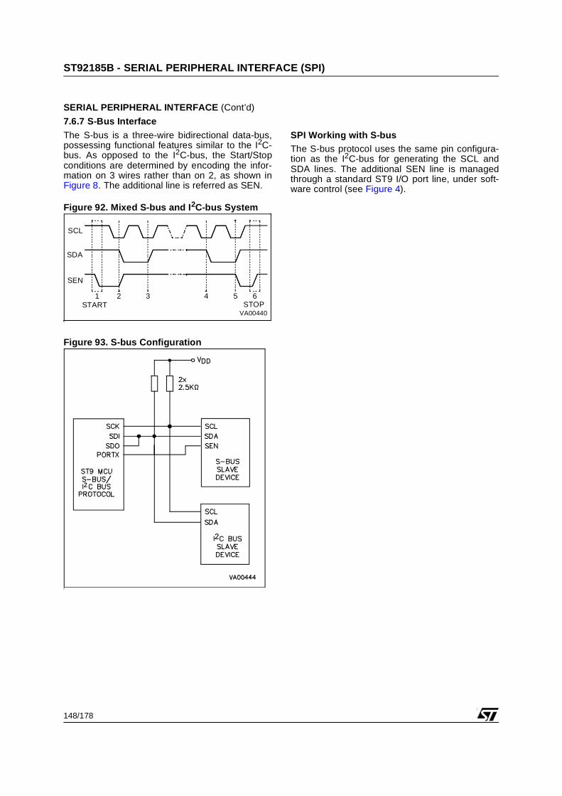
148/178
ST92185B - SERIAL PERIPHERAL INTERFACE (SPI)
SERIAL PERIPHERAL INTERFACE (Cont’d)
7.6.7 S-Bus Interface
The S-bus is a three-wire bidirectional data-bus,possessing functional features similar to the I2C-bus. As opposed to the I2C-bus, the Start/Stopconditions are determined by encoding the infor-mation on 3 wires rather than on 2, as shown inFigure 8. The additional line is referred as SEN.
SPI Working with S-busThe S-bus protocol uses the same pin configura-tion as the I2C-bus for generating the SCL andSDA lines. The additional SEN line is managedthrough a standard ST9 I/O port line, under soft-ware control (see Figure 4).
Figure 92. Mixed S-bus and I2C-bus System
n
Figure 93. S-bus Configuration
n
1 2 3 4 5 6START STOP
VA00440
SCL
SDA
SEN

149/178
ST92185B - SERIAL PERIPHERAL INTERFACE (SPI)
SERIAL PERIPHERAL INTERFACE (Cont’d)
7.6.8 IM-bus Interface
The IM-bus features a bidirectional data line and aclock line; in addition, it requires an IDENT line todistinguish an address byte from a data byte (Fig-ure 10). Unlike the I2C-bus protocol, the IM-busprotocol sends the least significant bit first; this re-quires a software routine which reverses the bit or-der before sending, and after receiving, a databyte. Figure 9 shows the connections between anIM-bus peripheral and an ST9 SPI. The SDO andSDI pins are connected to the bidirectional datapin of the peripheral device. The SDO alternatefunction is configured as Open-Drain (external2.5KΩ pull-up resistors are required).
With this type of configuration, data is sent to theperipheral by writing the data byte to the SPIDRregister. To receive data from the peripheral, theuser should write FFh to the SPIDR register, in or-der to generate the shift clock pulses. As the SDO
line is set to the Open-Drain configuration, the in-coming data bits that are set to “1” do not affect theSDO/SDI line status (which defaults to a high leveldue to the FFh value in the transmit register), whileincoming bits that are set to “0” pull the input linelow.
In software it is necessary to initialise the ST9 SPIby setting both CPOL and CPHA to “1”. By using ageneral purpose I/O as the IDENT line, and forcingit to a logical “0” when writing to the SPIDR regis-ter, an address is sent (or read). Then, by settingthis bit to “1” and writing to SPIDR, data is sent tothe peripheral. When all the address and datapairs are sent, it is necessary to drive the IDENTline low and high to create a short pulse. This willgenerate the stop condition.
Figure 94. ST9 and IM-bus Peripheral
n
Figure 95. IM bus Timing
VDD
SCKSDI
SDO
ST9 MCUIM-BUS
CLOCKDATAIDENT
IM-BUSSLAVEDEVICE
PROTOCOL
PORTX
VR001427
2.5 K2x
1 2 3 4 5 6
CLOCK LINE
DATA LINE 1 2 43 5 6 MSB
VR000172
MSBLSB LSB
IDENT

150/178
ST92185B - SERIAL PERIPHERAL INTERFACE (SPI)
SERIAL PERIPHERAL INTERFACE (Cont’d)
7.6.9 Register Description
It is possible to have up to 3 independent SPIs inthe same device (refer to the device block dia-gram). In this case they are named SPI0 thruSPI2. If the device has one SPI converter it usesthe register adresses of SPI0. The register map isthe following:
Note: In the register description on the followingpages, register and page numbers are given usingthe example of SPI0.
SPI DATA REGISTER (SPIDR)R253 - Read/WriteRegister Page: 0Reset Value: undefined
Bit 7:0 = D[0:7]: SPI Data.This register contains the data transmitted and re-ceived by the SPI. Data is transmitted bit 7 first,and incoming data is received into bit 0. Transmis-sion is started by writing to this register.
Note: SPIDR state remains undefined until theend of transmission of the first byte.
SPI CONTROL REGISTER (SPICR)R254 - Read/WriteRegister Page: 0Reset Value: 0000 0000 (00h)
Bit 7 = SPEN: Serial Peripheral Enable.0: SCK and SDO are kept tristate.
1: Both alternate functions SCK and SDO are ena-bled.
Note: furthermore, SPEN (together with the BMSbit) affects the selection of the source for interruptchannel B0. Transmission starts when data is writ-ten to the SPIDR Register.
Bit 6 = BMS: S-bus/I2C-bus Mode Selector.0: Perform a re-initialisation of the SPI logic, thus
allowing recovery procedures after a RX/TX fail-ure.
1: Enable S-bus/I2C-bus arbitration, clock synchro-nization and Start/ Stop detection (SPI used inan S-bus/I2C-bus protocol).
Note: when the BMS bit is reset, it affects (togeth-er with the SPEN bit) the selection of the sourcefor interrupt channel B0.
Bit 5 = ARB: Arbitration flag bit.This bit is set by hardware and can be reset bysoftware. 0: S-bus/I2C-bus stop condition is detected.1: Arbitration lost by the SPI in S-bus/I2C-bus
mode.
Note: when ARB is set automatically, the SDO pinis set to a high value until a write instruction onSPIDR is performed.
Bit 4 = BUSY: SPI Busy Flag.This bit is set by hardware. It allows the user tomonitor the SPI status by polling its value.0: No transmission in progress.1: Transmission in progress.
Bit 3 = CPOL: Transmission Clock Polarity.CPOL controls the normal or steady state value ofthe clock when data is not being transferred.Please refer to the following table and to Figure 11to see this bit action (together with the CPHA bit).
Note: As the SCK line is held in a high impedancestate when the SPI is disabled (SPEN = “0”), theSCK pin must be connected to VSS or to VCCthrough a resistor, depending on the CPOL state.Polarity should be set during the initialisation rou-tine, in accordance with the setting of all peripher-als, and should not be changed during programexecution.
Register SPIn Page
SPIDR R253 SPI0 0
SPICR R254 SPI0 0
SPIDR1 R253 SPI1 7
SPICR1 R254 SPI1 7
SPIDR2 R245 SPI2 7
SPICR2 R246 SPI2 7
7 0
D7 D6 D5 D4 D3 D2 D1 D0
7 0
SPEN BMS ARB BUSY CPOL CPHA SPR1 SPR0

151/178
ST92185B - SERIAL PERIPHERAL INTERFACE (SPI)
SERIAL PERIPHERAL INTERFACE (Cont’d)
Bit 2 = CPHA: Transmission Clock Phase.CPHA controls the relationship between the dataon the SDI and SDO pins, and the clock signal onthe SCK pin. The CPHA bit selects the clock edgeused to capture data. It has its greatest impact onthe first bit transmitted (MSB), because it does (ordoes not) allow a clock transition before the firstdata capture edge. Figure 11 shows the relation-ship between CPHA, CPOL and SCK, and indi-cates active clock edges and strobe times.
Bit 1:0 = SPR[1:0]: SPI Rate. These two bits select one (of four) baud rates, tobe used as SCK.
Figure 96. SPI Data and Clock Timing
CPOL CPHASCK
(in Figure 11)
0011
0101
(a)(b)(c)(d)
SPR1 SPR0Clock
DividerSCK Frequency
(@ INTCLK = 24MHz)
0011
0101
816128256
3000kHz1500kHz187.5kHz93.75kHz
(T = 0.33µs)(T = 0.67µs)(T = 5.33µs)(T = 10.66µs)

152/178
ST92185B - A/D CONVERTER (A/D)
7.7 A/D CONVERTER (A/D)
7.7.1 Introduction
The 8 bit Analog to Digital Converter uses a fullydifferential analog configuration for the best noiseimmunity and precision performance. The analogvoltage references of the converter are connectedto the internal AVDD & AVSS analog supply pins ofthe chip if they are available, otherwise to the ordi-nary VDD and VSS supply pins of the chip. Theguaranteed accuracy depends on the device (seeElectrical Characteristics). A fast Sample/Hold al-lows quick signal sampling for minimum warpingeffect and conversion error.
7.7.2 Main Features 8-bit resolution A/D Converter Single Conversion Time (including Sampling
Time):
– 138 internal system clock periods in slowmode (~5.6 µs @25Mhz internal systemclock);
– 78 INTCLK periods in fast mode (~6.5 µs @12MHZ internal system clock)
Sample/Hold: Tsample=
– 84 INTCLK periods in slow mode (~3.4 µs@25Mhz internal system clock)
– 48 INTCLK periods in fast mode (~4 µs@12Mhz internal system clock)
Up to 4 Analog Inputs (the number of inputs isdevice dependent, see device pinout)
Single/Continuous Conversion Mode External/Internal source Trigger (Alternate
synchronization) Power Down mode (Zero Power Consumption) 1 Control Logic Register 1 Data Register
7.7.3 General Description
Depending on the device, up to 8 analog inputscan be selected by software.
Different conversion modes are provided: single,continuous, or triggered. The continuous modeperforms a continuous conversion flow of the se-lected channel, while in the single mode the se-lected channel is converted once and then the log-ic waits for a new hardware or software restart.
A data register (ADDTR) is available, mapped inpage 62, allowing data storage (in single or contin-uous mode).
The start conversion event can be managed bysoftware, writing the START/STOP bit of the Con-trol Logic Register or by hardware using either:
– An external signal on the EXTRG triggered input (negative edge sensitive) connected as an Alter-nate Function to an I/O port bit
– An On Chip Event generated by another periph-eral, such as the MFT (Multifunction Timer).
Figure 97. A/D Converter Block Diagramn
ST
9 B
US
SUCCESSIVEAPPROXIMATION
REGISTER
ANALOGMUX
DATAREGISTER
CONTROL LOGIC
S/H
Ain1
Ainx
INTRG(On Chip Event)
Ain0
EXTRG

153/178
ST92185B - A/D CONVERTER (A/D)
A/D CONVERTER (Cont’d)
The conversion technique used is successive ap-proximation, with AC coupled analog fully differen-tial comparators blocks plus a Sample and Holdlogic and a reference generator.
The internal reference (DAC) is based on the useof a binary-ratioed capacitor array. This techniqueallows the specified monotonicity (using the sameratioed capacitors as sampling capacitor). A Pow-er Down programmable bit sets the A/D converteranalog section to a zero consumption idle status.
7.7.3.1 Operating Modes The two main operating modes, single and contin-uous, can be selected by writing 0 (reset value) or1 into the CONT bit of the Control Logic Register.
Single ModeIn single mode (CONT=0 in ADCLR) the STR bit isforced to '0' after the end of channel i-th conver-sion; then the A/D waits for a new start event. Thismode is useful when a set of signals must be sam-pled at a fixed frequency imposed by a Timer unitor an external generator (through the alternatesynchronization feature). A simple software rou-tine monitoring the STR bit can be used to savethe current value before a new conversion ends(so to create a signal samples table within the in-ternal memory or the Register File). Furthermore,if the R242.0 bit (register AD-INT, bit 0) is set, atthe end of conversion a negative edge on the con-nected external interrupt channel (see InterruptsChapter) is generated to allow the reading of theconverted data by means of an interrupt routine.
Continuous ModeIn continuous mode (CONT=1 in ADCLR) a con-tinuous conversion flow is entered by a start eventon the selected channel until the STR bit is resetby software.
At the end of each conversion, the Data Register(ADCDR) content is updated with the last conver-sion result, while the former value is lost. When theconversion flow is stopped, an interrupt request isgenerated with the same modality previously de-scribed.
7.7.3.2 Alternate SynchronizationThis feature is available in both single/continuousmodes. The negative edge of external EXTRG sig-nal or the occurrence of an on-chip event generat-ed by another peripheral can be used to synchro-nize the conversion start with a trigger pulse.
These events can be enabled or masked by pro-gramming the TRG bit in the ADCLR Register.
The effect of alternate synchronization is to set theSTR bit, which is cleared by hardware at the end ofeach conversion in single mode. In continuousmode any trigger pulse following the first one willbe ignored. The synchronization source must pro-vide a pulse (1.5 internal system clock, 125ns @12 MHz internal clock) of minimum width, and aperiod greater (in single mode) than the conver-sion time (~6.5us @ 12 MHz internal clock). If atrigger occurs when the STR bit is still '1' (conver-sions still in progress), it is ignored (see ElectricalCharacteristics).
WARNING: If the EXTRG or INTRG signals are al-ready active when TRG bit is set, the conversionstarts immediately.
7.7.3.3 Power-Up Operations
Before enabling any A/D operation mode, set thePOW bit of the ADCLR Register at least 60 µs be-fore the first conversion starts to enable the bias-ing circuits inside the analog section of the con-verter. Clearing the POW bit is useful when the A/D is not used so reducing the total chip powerconsumption. This state is also the reset configu-ration and it is forced by hardware when the core isin HALT state (after a HALT instruction execution).
7.7.3.4 Register Mapping
It is possible to have two independent A/D convert-ers in the same device. In this case they arenamed A/D 0 and A/D 1. If the device has one A/Dconverter it uses the register addresses of A/D 0.The register map is the following:
If two A/D converters are present, the registers arerenamed, adding the suffix 0 to the A/D 0 registersand 1 to the A/D 1 registers.
Register Address ADn Page 62 (3Eh)
F0h A/D 0 ADDTR0
F1h A/D 0 ADCLR0
F2h A/D 0 ADINT0
F3-F7h A/D 0 Reserved
F8h A/D 1 ADDTR1
F9h A/D 1 ADCLR1
FAh A/D 1 ADINT1
FB-FFh A/D 1 Reserved

154/178
ST92185B - A/D CONVERTER (A/D)
A/D CONVERTER (Cont’d)
7.7.4 Register Description
A/D CONTROL LOGIC REGISTER (ADCLR)R241 - Read/WriteRegister Page: 62Reset value: 0000 0000 (00h)
This 8-bit register manages the A/D logic opera-tions. Any write operation to it will cause the cur-rent conversion to be aborted and the logic to bere-initialized to the starting configuration.
Bit 7:5 = C[2:0]: Channel Address.These bits are set and cleared by software. Theyselect channel i conversion as follows:
Bit 4 = FS: Fast/Slow. This bit is set and cleared by software.0: Fast mode. Single conversion time: 78 x
INTCLK (5.75µs at INTCLK = 12 MHz)1: Slow mode. Single conversion time: 138 x
INTCLK (11.5µs at INTCLK = 12 MHz)
Note: Fast conversion mode is only allowed for in-ternal speeds which do not exceed 12 MHz.
Bit 3 = TRG: External/Internal Trigger Enable. This bit is set and cleared by software.
0: External/Internal Trigger disabled.1: Either a negative (falling) edge on the EXTRG
pin or an On Chip Event writes a “1” into the STR bit, enabling start of conversion.
Note: Triggering by on chip event is available ondevices with the multifunction timer (MFT) periph-eral.
Bit 2 = POW: Power Enable.This bit is set and cleared by software.0: Disables all power consuming logic.1: Enables the A/D logic and analog circuitry.
Bit 1 = CONT: Continuous/Single Mode Select.This bit it set and cleared by software.0: Single mode: after the current conversion ends,
the STR bit is reset by hardware and the con-verter logic is put in a wait status. To start anoth-er conversion, the STR bit has to be set by soft-ware or hardware.
1: Select Continuous Mode, a continuous flow of A/D conversions on the selected channel, start-ing when the STR bit is set.
Bit 0 = STR: Start/Stop.This bit is set and cleared by software. It is also setby hardware when the A/D is synchronized with anexternal/internal trigger.0: Stop conversion on channel i. An interrupt is
generated if the STR was previously set and the AD-INT bit is set.
1: Start conversion on channel i
WARNING: When accessing this register, it is rec-ommended to keep the related A/D interrupt chan-nel masked or disabled to avoid spurious interruptrequests.
7 0
C2 C1 C0 FS TRG POW CONT STR
C2 C1 C0 Channel Enabled00001
00110
01010
Channel 0 Channel 1Channel 2Channel 4Channel 3

155/178
ST92185B - A/D CONVERTER (A/D)
A/D CONVERTER (Cont’d)
A/D CHANNEL i DATA REGISTER (ADDTR)R240 - Read/WriteRegister Page: 62Reset value: undefined
The result of the conversion of the selected chan-nel is stored in the 8-bit ADDTR, which is reloadedwith a new value every time a conversion ends.
Bit 7:0 = R[7:0]: Channel i conversion result.
A/D INTERRUPT REGISTER (ADINT) Register Page: 62R242 - Read/writeReset value: 0000 0001 (01h)
Bit 7:1 = Reserved.
Bit 0 = AD-INT: AD Converter Interrupt Enable.
This bit is set and cleared by software. It allows theinterrupt source to be switched between the A/DConverter and an external interrupt pin (See Inter-rupts chapter).0: A/D Interrupt disabled. External pin selected as
interrupt source.1: A/D Interrupt enabled
7 0
R.7 R.6 R.5 R.4 R.3 R.2 R.1 R.0
7 0
0 0 0 0 0 0 0 AD-INT

156/178
ST92185B - VOLTAGE SYNTHESIS TUNING CONVERTER (VS)
7.8 VOLTAGE SYNTHESIS TUNING CONVERTER (VS)
7.8.1 Description
The on-chip Voltage Synthesis (VS) converter al-lows the generation of a tuning reference voltagein a TV set application. The peripheral is com-posed of a 14-bit counter that allows the conver-sion of the digital content in a tuning voltage, avail-able at the VS output pin, by using PWM (PulseWidth Modulation) and BRM (Bit Rate Modulation)techniques. The 14-bit counter gives 16384 stepswhich allow a resolution of approximately 2 mVover a tuning voltage of 32 V. This corresponds toa tuning resolution of about 40 KHz per step inUHF band (the actual value will depend on thecharacteristics of the tuner).
The tuning word consists of a 14-bit word con-tained in the registers VSDR1 (R254) and VSDR2(R255) both located in page 59.
Coarse tuning (PWM) is performed using the sev-en most significant bits. Fine tuning (BRM) is per-formed using the the seven least significant bits.With all “0”s loaded, the output is 0. As the tuningvoltage increases from all “0”s, the number of puls-es in one period increases to 128 with all pulsesbeing the same width. For values larger than 128,the PWM takes over and the number of pulses inone period remains constant at 128, but the widthchanges. At the other end of the scale, when al-most all “1”s are loaded, the pulses will start to linktogether and the number of pulses will decrease.
When all “1”s are loaded, the output will be almost100% high but will have a low pulse (1/16384 ofthe high pulse).
7.8.2 Output Waveforms
Included inside the VS are the register latches, areference counter, PWM and BRM control circuit-ry. The clock for the 14-bit reference counter is de-rived from the main system clock (referred to asINTCLK) after a division by 4. For example, usingan internal 12 MHz on-chip clock (see Timing &Clock Controller chapter) leads to a 3 MHz inputfor the VS counter.
From the point of view of the circuit, the sevenmost significant bits control the coarse tuning,while the seven least significant bits control thefine tuning. From the application and softwarepoint of view, the 14 bits can be considered as onebinary number.
As already mentioned the coarse tuning consistsof a PWM signal with 128 steps: we can considerthe fine tuning to cover 128 coarse tuning cycles.
The VS Tuning Converter is implemented with 2separate outputs (VSO1 and VSO2) that can drive2 separate Alternate Function outputs of 2 stand-ard I/O port bits. A control bit allows you to choosewhich output is activated (only one output can beactivated at a time).
When a VS output is not selected because the VSis disabled or because the second output is select-ed, it stays at a logical “one” level, allowing you touse the corresponding I/O port bit either as a nor-mal I/O port bit or for a possible second AlternateFunction output.
A second control bit allows the VS function to bestarted (or stopped) by software.

157/178
ST92185B - VOLTAGE SYNTHESIS TUNING CONVERTER (VS)
VOLTAGE SYNTHESIS (Cont’d)
PWM Generation
The counter increments continuously, clocked atINTCLK divided by 4. Whenever the 7 least signif-icant bits of the counter overflow, the VS output isset.
The state of the PWM counter is continuouslycompared to the value programmed in the 7 mostsignificant bits of the tuning word. When a matchoccurs, the output is reset thus generating thePWM output signal on the VS pin.
This Pulse Width modulated signal must be fil-tered, using an external RC network placed asclose as possible to the associated pin. This pro-vides an analog voltage proportional to the aver-age charge passed to the external capacitor. Thusfor a higher mark/space ratio (High time much
greater than Low time) the average output voltageis higher. The external components of the RC net-work should be selected for the filtering level re-quired for control of the system variable.
Figure 98. Typical PWM Output Filter
Figure 99. PWM Generation
Cext
OUTPUTVOLTAGE
Rext
PWM OUT1K
COUNTER
127
7-BIT PWMVALUE
OVERFLOWOVERFLOW OVERFLOW
000 t
PWM OUTPUT t
INTCLK/4 x 128

158/178
ST92185B - VOLTAGE SYNTHESIS TUNING CONVERTER (VS)
VOLTAGE SYNTHESIS (Cont’d)
Figure 100. PWM Simplified Voltage Output After Filtering (2 examples)
V DD
0V
0V
DDV Vripple (mV)
VOUTAVG
"CHARGE" "DISCHARGE" "CHARGE" "DISCHARGE"
0V
V
V
0V OUTAVGV
(mV)rippleV
VR01956"CHARGE" "DISCHARGE" "CHARGE" "DISCHARGE"
PWMOUT
DD
DD
PWMOUT
OUTPUTVOLTAGE
OUTPUTVOLTAGE

159/178
ST92185B - VOLTAGE SYNTHESIS TUNING CONVERTER (VS)
VOLTAGE SYNTHESIS (Cont’d)
BRM Generation
The BRM bits allow the addition of a pulse to wid-en a standard PWM pulse for specific PWM cy-cles. This has the effect of “fine-tuning” the PWMDuty cycle (without modifying the base duty cycle),thus, with the external filtering, providing additionalfine voltage steps.
The incremental pulses (with duration of TINTCLK/4) are added to the beginning of the original PWMpulse and thus cause the PWM high time to be ex-tended by this time with a corresponding reductionin the low time. The PWM intervals which are add-ed to are specified in the lower 7 bits of the tuningword and are encoded as shown in the followingtable.
Table 29. 7-Bit BRM Pulse Addition Positions
The BRM values shown may be combined togeth-er to provide a summation of the incremental pulseintervals specified.
The pulse increment corresponds to the PWM res-olution.
Figure 101. Simplified Filtered Voltage Output Schematic with BRM added
Fine TuningNo. of Pulses added at the
following Cycles
0000001 64
0000010 32, 96
0000100 16, 48, 80, 112
0001000 8, 24,... 104, 120
0010000 4, 12,... 116, 124
0100000 2, 6,... 122, 126
1000000 1, 3,... 125, 127
VDD
PWMOUT
0V
VDD
OUTPUT
VOLTAGE
0V
BRM = 1
BRM = 0
TINTCLK/4
BRM
EXTENDED PULSE
= = =

160/178
ST92185B - VOLTAGE SYNTHESIS TUNING CONVERTER (VS)
VOLTAGE SYNTHESIS (Cont’d)
7.8.3 Register Description
VS DATA AND CONTROL REGISTER 1(VSDR1)R254 - Read/WriteRegister Page: 59Reset Value: 0000 0000 (00h)
Bit 7 = VSE: VS enable bit.0: VS Tuning Converter disabled (i.e. the clock is
not forwarded to the VS counter and the 2 out-puts are set to 1 (idle state)
1: VS Tuning Converter enabled.
Bit 6 = VSWP: VS Output SelectThis bit controls which VS output is enabled to out-put the VS signal. 0: VSO1 output selected1: VSO2 output selected
Bit 5:0 = VD[13:8] Tuning word bits. These bits are the 6 most significant bits of theTuning word forming the PWM selection. TheVD13 bit is the MSB.
VS DATA AND CONTROL REGISTER 2(VSDR2)R255 - Read/WriteRegister Page: 59Reset Value: 0000 0000 (00h)
Bit 7:0 = VD[7:0] Tuning word bits.These bits are the 8 least significant data bits ofthe VS Tuning word. All bits are accessible. BitsVD6 - VD0 form the BRM pulse selection. VD7 isthe LSB of the 7 bits forming the PWM selection.
7 6 5 4 3 2 1 0
VSE VSWP VD13 VD12 VD11 VD10 VD9 VD8
7 0
VD7 VD6 VD5 VD4 VD3 VD2 VD1 VD0

161/178
ST92185B - PWM GENERATOR
7.9 PWM GENERATOR
7.9.1 Introduction
The PWM (Pulse Width Modulated) signal genera-tor allows the digital generation of up to 8 analogoutputs when used with an external filtering net-work.
The unit is based around an 8-bit counter which isdriven by a programmable 4-bit prescaler, with aninput clock signal equal to the internal clockINTCLK divided by 2. For example, with a 12 MHzInternal clock, using the full 8-bit resolution, a fre-
quency range from 1465 Hz up to 23437 Hz canbe achieved.Higher frequencies, with lower resolution, can beachieved by using the autoclear register. As an ex-ample, with a 12 MHz Internal clock, a maximumPWM repetition rate of 93750 Hz can be reachedwith 6-bit resolution.Note: The number of output pins is device de-pendant. Refer to the device pinout description.
Figure 102. PWM Block Diagram.
Autoclear
Compare 7
Compare 6
Compare 5
Compare 4
Compare 3
Compare 2
Compare 1
Compare 0
VR01765
PWM7
PWM0
8 Bit Counter 4 Bit Presc.
Control LogicINTCLK/2
OU
TP
UT
LO
GIC
ST
9 R
egi
ster
Bus

162/178
ST92185B - PWM GENERATOR
PWM GENERATOR (Cont’d)
Up to 8 PWM outputs can be selected as AlternateFunctions of an I/O port. Each output bit is inde-pendently controlled by a separate Compare Reg-ister. When the value programmed into the Com-pare Register and the counter value are equal, thecorresponding output bit is set. The output bit is re-set by a counter clear (by overflow or autoclear),generating the variable PWM signal.
Each output bit can also be complemented or dis-abled under software control.
7.9.2 Register Mapping
The ST9 can have one or two PWM Generators.Each has 13 registers mapped in page 59 (PWM0)or page 58 (PWM1). In the register description onthe following pages, the register page refers toPWM0 only.
Figure 103. PWM Action When Compare Register = 0 (no complement)
Figure 104. PWM Action When Compare Register = 3 (no complement)
Register Address
Register Function
R240 CM0 Ch. 0 Compare Register
R241 CM1 Ch. 1 Compare Register
R242 CM2 Ch. 2 Compare Register
R243 CM3 Ch. 3 Compare Register
R244 CM4 Ch. 4 Compare Register
R245 CM5 Ch. 5 Compare Register
R246 CM6 Ch. 6 Compare Register
R247 CM7 Ch. 7 Compare Register
R248 ACR Autoclear Register
R249 CRR Counter Read Register
R250 PCTLR Prescaler/ Reload Reg.
R251 OCPLR Output Complement Reg.
R252 OER Output Enable Register
R253- R255 — Reserved
VR0A1814
PWM CLOCK
PWMOUTPUT
Counter=Autoclear value Counter=0 Counter=1
VR001814
PWM CLOCK
PWMOUTPUT
Counter=Autoclear value Counter=0 Counter=3

163/178
ST92185B - PWM GENERATOR
PWM GENERATOR (Cont’d)
7.9.2.1 Register Description
COMPARE REGISTER 0 (CM0)R240 - Read/WriteRegister Page: 59Reset Value: 0000 0000 (00h)
This is the compare register controlling PWM out-put 0. When the programmed content is equal tothe counter content, a SET operation is performedon PWM output 0 (if the output has not been com-plemented or disabled).
Bit 7:0 = CM0.[7:0]: PWM Compare value Chan-nel 0.
COMPARE REGISTER 1 (CM1)R241 - Read/WriteRegister Page: 59Reset Value: 0000 0000 (00h)
This is the compare register controlling PWM out-put 1.
COMPARE REGISTER 2 (CM2)R242 - Read/WriteRegister Page: 59Reset Value: 0000 0000 (00h)
This is the compare register controlling PWM out-put 2.
COMPARE REGISTER 3 (CM3)R243 - Read/WriteRegister Page: 59Reset Value: 0000 0000 (00h)
This is the compare register controlling PWM out-put 3.
COMPARE REGISTER 4 (CM4)R244 - Read/WriteRegister Page: 59Reset Value: 0000 0000 (00h)
This is the compare register controlling PWM out-put 4.
COMPARE REGISTER 5 (CM5)R245 - Read/WriteRegister Page: 59Reset Value: 0000 0000 (00h)
This is the compare register controlling PWM out-put 5.
COMPARE REGISTER 6 (CM6)R246 - Read/WriteRegister Page: 59Reset Value: 0000 0000 (00h)
This is the compare register controlling PWM out-put 6.
COMPARE REGISTER 7 (CM7)R247 - Read/WriteRegister Page: 59Reset Value: 0000 0000 (00h)
This is the compare register controlling PWM out-put 7.
7 0
CM0.7 CM0.6 CM0.5 CM0.4 CM0.3 CM0.2 CM0.1 CM0.0
7 0
CM1.7 CM1.6 CM1.5 CM1.4 CM1.3 CM1.2 CM1.1 CM1.0
7 0
CM2.7 CM2.6 CM2.5 CM2.4 CM2.3 CM2.2 CM2.1 CM2.0
7 0
CM3.7 CM3.6 CM3.5 CM3.4 CM3.3 CM3.2 CM3.1 CM3.0
7 0
CM4.7 CM4.6 CM4.5 CM4.4 CM4.3 CM4.2 CM4.1 CM4.0
7 0
CM5.7 CM5.6 CM5.5 CM5.4 CM5.3 CM5.2 CM5.1 CM5.0
7 0
CM6.7 CM6.6 CM6.5 CM6.4 CM6.3 CM6.2 CM6.1 CM6.0
7 0
CM7.7 CM7.6 CM7.5 CM7.4 CM7.3 CM7.2 CM7.1 CM7.0

164/178
ST92185B - PWM GENERATOR
PWM GENERATOR (Cont’d)
AUTOCLEAR REGISTER (ACR)R248 - Read/WriteRegister Page: 59Reset Value: 1111 1111 (FFh)
This register behaves exactly as a 9th compareRegister, but its effect is to clear the CRR counterregister, so causing the desired PWM repetitionrate.
The reset condition generates the free runningmode. So, FFh means count by 256.
Bit 7:0 = AC[7:0]: Autoclear Count Value.
When 00 is written to the Compare Register, if theACR register = FFh, the PWM output bit is alwaysset except for the last clock count (255 set and 1reset; the converse when the output is comple-mented). If the ACR content is less than FFh, thePWM output bit is set for a number of clock countsequal to that content (see Figure 2).
Writing the Compare register constant equal to theACR register value causes the output bit to be al-ways reset (or set if complemented).
Example: If 03h is written to the Compare Regis-ter, the output bit is reset when the CRR counterreaches the ACR register value and set when itreaches the Compare register value (after 4 clockcounts, see Figure 3). The action will be reversedif the output is complemented. The PWM mark/space ratio will remain constant until changed bysoftware writing a new value in the ACR register.
COUNTER REGISTER (CRR)R249 - Read OnlyRegister Page: 59Reset Value: 0000 0000 (00h)
This read-only register returns the current countervalue when read.
The 8 bit Counter is initialized to 00h at reset, andis a free running UP counter.
Bit 7:0 = CR[7:0]: Current Counter Value.
PRESCALER AND CONTROL REGISTER(PCTL)R250 - Read/WriteRegister Page: 59Reset Value: 0000 1100 (0Ch)
Bit 7:4 = PR[3:0] PWM Prescaler value.These bits hold the Prescaler preset value. This isreloaded into the 4-bit prescaler whenever theprescaler (DOWN Counter) reaches the value 0,so determining the 8-bit Counter count frequency.The value 0 corresponds to the maximum counterfrequency which is INTCLK/2. The value Fh corre-sponds to the maximum frequency divided by 16(INTCLK/32).
The reset condition initializes the Prescaler to theMaximum Counter frequency.
Bit 3:2 = Reserved. Forced by hardware to “1”
Bit 1 = CLR: Counter Clear.This bit when set, allows both to clear the counter,and to reload the prescaler. The effect is also toclear the PWM output. It returns “0” if read.
Bit 0 = CE: Counter Enable.This bit enables the counter and the prescalerwhen set to “1”. It stops both when reset withoutaffecting their current value, allowing the count tobe suspended and then restarted by software “onfly”.
7 0
AC7 AC6 AC5 AC4 AC3 AC2 AC1 AC0
7 0
CR7 CR6 CR5 CR4 CR3 CR2 CR1 CR0
7 0
PR3 PR2 PR1 PR0 1 1 CLR CE
PR[3:0] Divider Factor Frequency
0 1 INTCLK/2 (Max.)
1 2 INTCLK/4
2 3 INTCLK/6
.. .. ..
Fh 16 INTCLK/32 (Min.)

165/178
ST92185B - PWM GENERATOR
PWM GENERATOR (Cont’d)
OUTPUT COMPLEMENT REGISTER (OCPL) R251- Read/WriteRegister Page 59Reset Value: 0000 0000 (00h)
This register allows the PWM output level to becomplemented on an individual bit basis.
In default mode (reset configuration), each com-parison true between a Compare register and thecounter has the effect of setting the correspondingoutput.
At counter clear (either by autoclear comparisontrue, software clear or overflow when in free run-ning mode), all the outputs are cleared.
By setting each individual bit (OCPL.x) in this reg-ister, the logic value of the corresponding outputwill be inverted (i.e. reset on comparison true andset on counter clear).
Example: When set to “1”, the OCPL.1 bit comple-ments the PWM output 1.
Bit 7 = OCPL.7: Complement PWM Output 7.
Bit 6 = OCPL.6: Complement PWM Output 6.Bit 5 = OCPL.5: Complement PWM Output 5.
Bit 4 = OCPL.4: Complement PWM Output 4.Bit 3 = OCPL.3: Complement PWM Output 3.
Bit 2 = OCPL.2: Complement PWM Output 2.
Bit 1 = OCPL.1: Complement PWM Output 1.Bit 0 = OCPL.0: Complement PWM Output 0.
OUTPUT ENABLE REGISTER (OER)R252 - Read/WriteRegister Page: 59Reset Value: 0000 0000 (00h)
These bits are set and cleared by software.0: Force the corresponding PWM output to logic
level 1. This allows the port pins to be used for normal I/O functions or other alternate functions (if available).
1: Enable the corresponding PWM output.
Example: Writing 03h into the OE Register will en-able only PWM outputs 0 and 1, while outputs 2, 3,4, 5, 6 and 7 will be forced to logic level “1”.
Bit 7 = OE.7: Output Enable PWM Output 7.
Bit 6 = OE.6: Output Enable PWM Output 6.
Bit 5 = OE.5: Output Enable PWM Output 5.Bit 4 = OE.4: Output Enable PWM Output 4.
Bit 3 = OE.3: Output Enable PWM Output 3.Bit 2 = OE.2: Output Enable PWM Output 2.
Bit 1 = OE.1: Output Enable PWM Output 1.Bit 0 = OE.0: Output Enable PWM Output 0.
7 0
OCPL.7OCPL.6OCPL.5 OCPL.4OCPL.3 OCPL.2OCPL.1OCPL.0
7 0
OE.7 OE.6 OE.5 OE.4 OE.3 OE.2 OE.1 OE.0

166/178
ST92185B - ELECTRICAL CHARACTERISTICS
8 ELECTRICAL CHARACTERISTICSABSOLUTE MAXIMUM RATINGS
Note: Stress above those listed as “Absolute maximum ratings” may cause permanent damage to the device. This is a stress rating only andfunctional operation of the device at these conditions is not implied. Exposure to maximum rating conditions for extended periods may affectdevice reliability.
RECOMMENDED OPERATING CONDITIONS
Symbol Parameter Value Unit
VDD Supply Voltage VSS - 0.3 to VSS + 6.5 V
VSSA Analog Ground VSS - 0.3 to VSS + 0.3 V
VDDA Analog Supply Voltage VDD -0.3 to VDD +0.3 V
VI Input Voltage VSS - 0.3 to VDD +0.3 V
VAI Analog Input Voltage (A/D Converter)VSS - 0.3 to VDD +0.3
VSSA - 0.3 to VDDA +0.3V
VO Output Voltage VSS - 0.3 to VDD + 0.3 V
TSTG Storage Temperature - 55 to + 150 °C
IINJ
Pin Injected Current
Maximum Accumulated Pin
Injected Current In Device
- 5 to + 5
- 50 to +5 0
mA
mA
Symbol ParameterValue
UnitMin. Max.
TA Operating Temperature 0 70 °C
VDD Supply Voltage 4.5 5.5 V
VDDA Analog Supply Voltage (PLL) 4.5 5.5 V
fOSCE External Oscillator Frequency 3.3 8.7 MHz
fOSCI Internal Clock Frequency (INTCLK) 24 MHz

167/178
ST92185B - ELECTRICAL CHARACTERISTICS
DC ELECTRICAL CHARACTERISTICS(VDD= 5V +/-10%; TA= 0 to 70°C; unless otherwise specified)
Symbol Parameter Test ConditionsValue
UnitMin. Max.
VIHCK Clock In high level External clock 0.7 VDD V
VILCK Clock in low level External clock 0.3 VDD V
VIH Input high level TTL 2.0 V
VIL Input low level TTL 0.8 V
VIH Input high level CMOS 0.8 VDD V
VIL Input low level CMOS 0.2 VDD V
VIHRS Reset in high level 0.7 VDD V
VILRS Reset in low level 0.3 VDD V
VHYRS Reset in hysteresis 0.3 V
VIHY P2.(1:0) input hysteresis 0.9 V
VIHVH HSYNC/VSYNC input high level 0.7 VDD V
VILVH HSYNC/VSYNC input low level 0.3 VDD V
VHYHV HSYNC/VSYNC input hysteresis 0.5 V
VOH Output high level Push-pull Ild=-0.8mA VDD-0.8 V
VOL Output low level Push-pull ld=+1.6mA 0.4 V
IWPU Weak pull-up current
bidir. state
VOL= 3V
VOL= 7V
50
350
µA
ILKIO I/O pin input leakage current 0<VIN<VDD -10 +10 µA
ILKRS Reset pin input 0<VIN<VDD -10 +10 µA
ILKAD A/D pin input leakage current alternate funct. op. drain -10 +10 µA
ILKOS OSCIN pin input leakage current 0<VIN<VDD -10 +10 µA

168/178
ST92185B - ELECTRICAL CHARACTERISTICS
AC ELECTRICAL CHARACTERISTICSPIN CAPACITANCE(VDD= 5V +/-10%; TA= 0 to 70°C; unless otherwise specified))
CURRENT CONSUMPTION(VDD= 5V +/-10%; TA= 0 to 70°C; unless otherwise specified)
Notes:1. Port 0 is configured in push-pull output mode (output is high). Ports 2, 3, 4 and 5 are configured in bi-directional weak pull-up mode resistor.
The external CLOCK pin (OSCIN) is driven by a square wave external clock at 8 MHz. The internal clock prescaler is in divide-by-1 mode.2. The CPU is fed by a 24 MHz frequency issued by the Main Clock Controller. VSYNC is tied to VSS, HSYNC is driven by a 15625Hz clock.
All peripherals working including Display.3. The CPU is fed by a 24 MHz frequency issued by the Main Clock Controller. VSYNC is tied to VSS, HSYNC is driven by a 15625Hz clock.
The TDSRAM interface and the Slicers are working; the Display controller is not working.4. VSYNC and HSYNC tied to VSS. External CLOCK pin (OSCIN) is hold low. All peripherals are disabled.
EXTERNAL INTERRUPT TIMING TABLE (rising or falling edge mode)(VDD= 5V +/-10%; TA= 0 to 70°C; unless otherwise specified))
TpC is the INTCLK clock period.
Symbol Parameter ConditionsValue
Unitmin max
CIO Pin Capacitance Digital Input/Output 10 pF
Symbol Parameter ConditionsValue
Unitmin typ. max
IDD1 Run Mode Current notes 1,2; all On 70 100 mA
IDDA1Run Mode Analog Current(pin VDDA)
Timing Controller On 35 50 mA
IDD2 HALT Mode Current notes 1,4 10 100 µA
IDDA2 HALT Mode Analog Current (pin VDDA)
notes 1,4 40 100 µA
Symbol ParameterConditions Value Unit
INTCLK=24 MHz. min max
TwLR low level pulse width TpC+12 95 ns
TwHR high level pulse width TpC+12 95 ns

169/178
ST92185B - ELECTRICAL CHARACTERISTICS
AC ELECTRICAL CHARACTERISTICS (Cont’d)
SPI TIMING TABLE(VDD= 5V +/-10%; TA= 0 to 70°C; Cload= 50pF)
(1) TpC is the OSCIN clock period; TpMC is the “Main Clock Frequency” period.
SKEW CORRECTOR TIMING TABLE(VDD= 5V +/-10%, TA= 0 to 70°C, unless otherwise specified)
(*) The OSD jitter is measured from leading edge to leading edge of a single character row on consecutive TV lines. The value is an envelopeof 100 fields
Symbol Parameter ConditionValue
Unitmin max
TsDI Input Data Set-up Time tbd ns
ThDI Input Data Hold Time (1) OSCIN/2 as internal Clock 1INTCLK +100ns ns
TdOV SCK to Output Data Valid tbd ns
ThDO Output Data Hold Time tbd ns
TwSKL SCK Low Pulse Width tbd ns
TwSKH SCK High Pulse Width tbd ns
Symbol Parameter Conditionsmax
ValueUnit
Tjskw Jitter on RGB output 36 MHz Skew corrector clock frequency 5* ns

170/178
ST92185B - ELECTRICAL CHARACTERISTICS
AC ELECTRICAL CHARACTERISTICS (Cont’d)
OSD DAC CHARACTERISTICS (ROM DEVICES ONLY)(VDD= 5V +/-10%, TA= 0 to 70°C, unless otherwise specified).
OSD DAC CHARACTERISTICS (EPROM AND OTP DEVICES ONLY)(VDD= 5V +/-10%, TA= 0 to 70°C, unless otherwise specified).
Symbol Parameter ConditionsValue
Unitmin typical max
Output impedance: FB,R,G,B 300 500 700 Ohm
Output voltage: FB,R,G,BCload= 20pF
RL = 100K
code= 111 1.000 1.250 V
code= 011 0.450 0.500 V
code= 000 0.025 0.080 V
FB= 1 2.4 2.7 3.4 V
FB= 0 0 0.025 0.080 V
Global voltage accuracy +/-5 %
Symbol Parameter ConditionsValue
Unitmin typical max
Output impedance: FB,R,G,B 300 500 700 Ohm
Output voltage: FB,R,G,BCload= 20pF
RL = 100K
code= 111 1.100 1.400 V
code= 011 0.600 0.800 V
code= 000 0.200 0.350 V
FB= 1 VDD-0.8 V
FB= 0 0.400 V
Global voltage accuracy +/-5 %

171/178
ST92185B - ELECTRICAL CHARACTERISTICS
AC ELECTRICAL CHARACTERISTICS (Cont’d)
A/D CONVERTER, EXTERNAL TRIGGER TIMING TABLE(VDD= 5V +/-10%; TA= 0 to 70°C; unless otherwise specified
A/D CONVERTER. ANALOG PARAMETERS TABLE(VDD= 5V +/-10%; TA= 0 to 70°C; unless otherwise specified))
Notes: (*) The values are expected at 25 Celsius degrees with VDD= 5V(**) ’LSBs’ , as used here, as a value of VDD/256(1) @ 24 MHz external clock(2) including Sample time(3) it must be considered as the on-chip series resistance before the sampling capacitor(4) DNL ERROR= max [V(i) -V(i-1)] / LSB-1 INL ERROR= max [V(i) -V(0)] / LSB-i
ABSOLUTE ACCURACY= overall max conversion error
Symbol ParameterOSCIN divide by
2;min/maxOSCIN divide by 1; min/max
ValueUnit
min max
Tlow Pulse Width1.5
INTCLKns
Thigh Pulse Distance ns
Text Period/fast Mode78+1
INTCLKµs
Tstr Start Conversion Delay 0.5 1.5 INTCLK
Core Clock issued by Timing Controller
Tlow Pulse Width ns
Thigh Pulse Distance ns
Text Period/fast Mode µs
Tstr Start Conversion Delay ns
ParameterValue Unit
Notetyp (*) min max (**)
Analog Input Range VSS VDD V
Conversion Time Fast/Slow 78/138 INTCLK (1,2)
Sample Time Fast/Slow 51.5/87.5 INTCLK (1)
Power-up Time 60 µs
Resolution 8 bits
Differential Non Linearity 3 5 LSBs (4)
Integral Non Linearity 4 5 LSBs (4)
Absolute Accuracy 2 3 LSBs (4)
Input Resistance 1.5 Kohm (3)
Hold Capacitance 1.92 pF

172/178
ST92185B - GENERAL INFORMATION
9 GENERAL INFORMATION
9.1 PACKAGE MECHANICAL DATA
Figure 105. 56-Pin Shrink Plastic Dual In Line Package, 600-mil Width
Figure 106. 42-Pin Shrink Plastic Dual In-Line Package, 600-mil Width
Dim.mm inches
Min Typ Max Min Typ Max
A 6.35 0.250
A1 0.38 0.015
A2 3.18 4.95 0.125 0.195
b 0.41 0.016
b2 0.89 0.035
C 0.20 0.38 0.008 0.015
D 50.29 53.21 1.980 2.095
E 15.01 0.591
E1 12.32 14.73 0.485 0.580
e 1.78 0.070
eA 15.24 0.600
eB 17.78 0.700
L 2.92 5.08 0.115 0.200
Number of Pins
N 56
PDIP56S
Dim.mm inches
Min Typ Max Min Typ Max
A 5.08 0.200
A1 0.51 0.020
A2 3.05 3.81 4.57 0.120 0.150 0.180
b 0.46 0.56 0.018 0.022
b2 1.02 1.14 0.040 0.045
C 0.23 0.25 0.38 0.009 0.010 0.015
D 36.58 36.83 37.08 1.440 1.450 1.460
E 15.24 16.00 0.600 0.630
E1 12.70 13.72 14.48 0.500 0.540 0.570
e 1.78 0.070
eA 15.24 0.600
eB 18.54 0.730
eC 0.00 1.52 0.000 0.060
L 2.54 3.30 3.56 0.100 0.130 0.140
Number of Pins
N 42
PDIP42S

173/178
ST92185B - GENERAL INFORMATION
PACKAGE MECHANICAL DATA (Cont’d)
Figure 107. 64-Pin Thin Quad Flat Package
Figure 108. 56-Pin Shrink Ceramic Dual In Line Package, 600-mil Width
Dimmm inches
Min Typ Max Min Typ Max
A 1.60 0.063
A1 0.05 0.15 0.002 0.006
A2 1.35 1.40 1.45 0.053 0.055 0.057
B 0.30 0.37 0.45 0.012 0.015 0.018
C 0.09 0.20 0.004 0.008
D 16.00 0.630
D1 14.00 0.551
D3 12.00 0.472
E 16.00 0.630
E1 14.00 0.551
E3 12.00 0.472
e 0.80 0.031
K 0° 3.5° 7°
L 0.45 0.60 0.75 0.018 0.024 0.030
L1 1.00 0.039
Number of Pins
N 64 ND 16 NE 16
L1L
K
Dim.mm inches
Min Typ Max Min Typ Max
A 4.17 0.164
A1 0.76 0.030
B 0.38 0.46 0.56 0.015 0.018 0.022
B1 0.76 0.89 1.02 0.030 0.035 0.040
C 0.23 0.25 0.38 0.009 0.010 0.015
D 50.04 50.80 51.56 1.970 2.000 2.030
D1 48.01 1.890
E1 14.48 14.99 15.49 0.570 0.590 0.610
e 1.78 0.070
G 14.12 14.38 14.63 0.556 0.566 0.576
G1 18.69 18.95 19.20 0.736 0.746 0.756
G2 1.14 0.045
G3 11.05 11.30 11.56 0.435 0.445 0.455
G4 15.11 15.37 15.62 0.595 0.605 0.615
L 2.92 5.08 0.115 0.200
S 1.40 0.055
Number of Pins
N 56
CDIP56SW

174/178
ST92185B - GENERAL INFORMATION
Figure 109. 42-Pin Shrink Ceramic Dual In-Line Package, 600-mil Width
Figure 110. 64-Pin Ceramic Quad Flat Package
Dim.mm inches
Min Typ Max Min Typ Max
A 4.01 0.158
A1 0.76 0.030
B 0.38 0.46 0.56 0.015 0.018 0.022
B1 0.76 0.89 1.02 0.030 0.035 0.040
C 0.23 0.25 0.38 0.009 0.010 0.015
D 36.68 37.34 38.00 1.444 1.470 1.496
D1 35.56 1.400
E1 14.48 14.99 15.49 0.570 0.590 0.610
e 1.78 0.070
G 14.12 14.38 14.63 0.556 0.566 0.576
G1 18.69 18.95 19.20 0.736 0.746 0.756
G2 1.14 0.045
G3 11.05 11.30 11.56 0.435 0.445 0.455
G4 15.11 15.37 15.62 0.595 0.605 0.615
L 2.92 5.08 0.115 0.200
S 0.89 0.035
Number of Pins
N 42
CDIP42SW
Dimmm inches
Min Typ Max Min Typ Max
A 3.27 0.129
A1 0.50 0.020
B 0.30 0.35 0.45 0.012 0.014 0.018
C 0.13 0.15 0.23 0.005 0.006 0.009
D 16.65 17.20 17.75 0.656 0.677 0.699
D1 13.57 13.97 14.37 0.534 0.550 0.566
D3 12.00 0.472
e 0.80 0.031
G 12.70 0.500
G2 0.96 0.038
L 0.35 0.80 0.014 0.031
0 8.31 0.327
Number of Pins
N 64CQFP064W

175/178
ST92185B - GENERAL INFORMATION
9.2 ORDERING INFORMATION
Each device is available for production in a userprogrammable version (OTP) as well as in factorycoded version (ROM). OTP devices are shipped tocustomer with a default blank content FFh, whileROM factory coded parts contain the code sent bycustomer. The common EPROM versions for de-bugging and prototyping features the maximummemory size and peripherals of the family. Caremust be taken to only use resources available onthe target device.
9.2.1 Transfer Of Customer Code
Customer code is made up of the ROM contentsand the list of the selected options (if any). TheROM contents are to be sent on diskette, or byelectronic means, with the hexadecimal file gener-ated by the development tool. All unused bytesmust be set to FFh.
Figure 111. ROM Factory Coded Device Types
DEVICE PACKAGETEMP.RANGE XXX/
Code name (defined by STMicroelectronics)
1= standard 0 to +70 °C
BN= Plastic SDIP56BJ= Plastic SDIP42T= Plastic TQFP64
ST92185B1ST92185B2ST92185B3

176/178
ST92185B - GENERAL INFORMATION
STMicroelectronics OPTION LIST
ST92185B
Customer: . . . . . . . . . . . . . . . . . . . . . . . . . . . .
Address: . . . . . . . . . . . . . . . . . . . . . . . . . . . .
. . . . . . . . . . . . . . . . . . . . . . . . . . . .
Contact: . . . . . . . . . . . . . . . . . . . . . . . . . . . .
Phone No: . . . . . . . . . . . . . . . . . . . . . . . . . . . .
Reference/ROM Code* : . . . . . . . . . . . . . . . . . .
*The ROM code name assigned by ST.
STMicroelectronics reference:
Device: [ ] ST92185B1B1
[ ] ST92185B2B1
[ ] ST92185B3B1
Package : [ ] SDIP42
[ ] SDIP56
[ ] TQFP64
Temperature Range : 0 to 70 C
Software Development: [ ] STMicroelectronics
[ ] Customer
[ ] External laboratory
Special Marking: [ ] No [ ] Yes "_ _ _ _ _ _ _ _ _ _ _ _ _ _ _ _"
For marking, one line is possible with maximum 14 characters. Authorized characters are let-ters, digits, ’.’, ’-’, ’/’ and spaces only.
Please consult your local ST Microelectronics sales office for other marking details if required.
Notes :
OSD Code : [ ] OSD File Filename [........ .OSD]
Quantity forecast : [..................] k units per year
For a period of : [..................] years
Preferred Production start dates : [../../..] (YY/MM/DD)
Date
Customer Signature :

177/178
ST92185B - REVISION HISTORY
10 REVISION HISTORY
Rev. Main Changes Date1.0 First release on DMS 01/11/00
1.116K ROM added / TQFP64 addedp1, changed device summary; added one feature (pin-compatible with...) and changed one feature (Pin-compatible EPROM, etc.). Added Option List.
03/15/00
1.2Added Section 10 on page 177. Updated Figure 3 on page 10 and Figure 5 on page 12. Changed Non-linearity values in A/D Converter Analog Parameters Table. Modified Table 9 on page 59. Modified Section 4.2 on page 57.
11 Oct 2001
1.3 Modification of the absolute maximum rating of the Supply Voltage value in Section 8 on page 166.16 Jan 2002

Information furnished is believed to be accurate and reliable. However, STMicroelectronics assumes no responsibility for the consequencesof use of such information nor for any infringement of patents or other rights of third parties which may result from its use. No license is grantedby implication or otherwise under any patent or patent rights of STMicroelectronics. Specifications mentioned in this publication are subjectto change without notice. This publication supersedes and replaces all information previously supplied. STMicroelectronics products are notauthorized for use as critical components in life support devices or systems without the express written approval of STMicroelectronics.
The ST logo is a registered trademark of STMicroelectronics
2003 STMicroelectronics - All Rights Reserved.
Purchase of I2C Components by STMicroelectronics conveys a license under the Philips I2C Patent. Rights to use these components in an I2C system is granted provided that the system conforms to the I2C Standard Specification as defined by Philips.
STMicroelectronics Group of CompaniesAustralia - Brazil - Canada - China - Finland - France - Germany - Hong Kong - India - Israel - Italy - Japan
Malaysia - Malta - Morocco - Singapore - Spain - Sweden - Switzerland - United Kingdom - U.S.A.
http://www.st.com


![INSTRUCTION MANUALtv.hitachi.eu/api/uploads/files/A01_[GB]_MB130S+E_43140... · 2018. 10. 17. · English - 5 - • Teletext • Headphone connection • Automatic programming system](https://img.dokumen.tips/doc/110x75/60ac9b95c649d809234bd88c/instruction-gbmb130se43140-2018-10-17-english-5-a-teletext-a.jpg)