Embed Size (px)
Citation preview

1
MAX24188
Low-Cost IEEE 1588 Clock
General Description
The MAX24188 is a flexible, low-cost IEEE 1588 clock designed to be the central 1588 time base in a multiport system. In such systems (typically boundary clocks or transparent clocks) timestampers at the ports must all have a common time and frequency reference. The MAX24188 serves as that common reference. As the system exchanges 1588 packets with an external 1588 master and calculates its time offset vs. the master, the MAX24188 can be adjusted by system software to zero out the time offset and thereby achieve time and frequency synchronization with the master. As the MAX24188 is adjusted, its output frequency and time alignment signals are correspondingly adjusted. All timestampers (and other time-aware components) that receive those signals then follow the adjustment to maintain synchronization with the MAX24188. In this way all 1588 elements in the system maintain a common sense of time and frequency.
The MAX24188 can be a stand-alone central timing function for 1588 systems. It can also be used in conjunction with one of Microsemi’s clock synchronization ICs in multimode systems designed to be clocked by 1588, 1588 plus frequency (such as synchronous Ethernet), or frequency only.
Applications
Central Time-Clock for 1588-Enabled Equipment with Timestamping on Multiple Ports
Wireless Base Stations and Controllers Switches, Routers, DSLAMs, PON Equipment Pseudowire Circuit Emulation Equipment Test and Measurement Systems Medical, Industrial, and Factory Automation Equipment
Ordering Information
PART TEMP RANGE PIN-PACKAGE
MAX24188ETK+ -40C to +85C 68 TQFN-EP*
+Denotes a lead-free/RoHS-compliant package. *EP = Exposed pad.
Block Diagram appears on page 4. Register Map appears on page 21.
Highlighted Features
Complete Hardware Support for IEEE 1588
Flexible Block for Any 1588 Architecture
Enables Ordinary, Boundary and Transparent Clocks
Steered by Software to Follow an External 1588 Master
2-8
ns Time Resolution and 2-32
ns Period Resolution
1ns Input Timestamp Accuracy and Output Edge Placement Accuracy
Three Time/Frequency Controls: Direct Time Write, Time Adjustment, and High-Resolution Frequency Adjustment
Programmable Clock and Time-Alignment I/O to Synchronize All 1588 Elements in the System
Can Provide an Output Clock Signal to Slave Components (125MHz/N , 1 ≤ N ≤ 255)
Can Provide an Output Time Alignment Signal to Slave Components (e.g. 1PPS)
Can Frequency-Lock to an Input Clock Signal from Elsewhere in the System
Can Timestamp an Input Time Alignment Signal to Time-Lock to a Master Elsewhere in the System (e.g., 1PPS)
Input Event Timestamper Detects Incoming Time Alignment (e.g., 1PPS) or Clock Edges, Can Timestamp Rising and/or Falling Edges
Flexible Programmable Event Generator (PEG) Can Output 1PPS (One Pulse per Period) or a Wide Variety of Clock Signals
Built-In Support for Telecom Equipment Timing Architectures with Dual Redundant Timing Cards
Full Support to Enable Switches and Routers to Be Transparent Clocks and/or Boundary Clocks
Full Support for 1588 and Synchronous Ethernet
Operates from a 10MHz, 12.8MHz, 25MHz, or 125MHz Reference Clock
SPI™ Processor Interface
1.2V Operation with 3.3V I/O
Data Sheet November 2016
_________________________________________________________________________________________________ MAX24188
2
TABLE OF CONTENTS
1. APPLICATION EXAMPLES .......................................................................................................... 4
2. BLOCK DIAGRAM ........................................................................................................................ 4
3. ACRONYMS AND ABBREVIATIONS ........................................................................................... 5
4. PIN DESCRIPTIONS ..................................................................................................................... 5
5. FUNCTIONAL DESCRIPTION ...................................................................................................... 8
5.1 GENERAL-PURPOSE I/O ................................................................................................................ 8 5.2 RESET, POWER DOWN AND PROCESSOR INTERRUPT ..................................................................... 9
5.2.1 Reset ...................................................................................................................................................... 9 5.2.2 Power Down ........................................................................................................................................... 9 5.2.3 Processor Interrupts ............................................................................................................................... 9
5.3 SPI - SERIAL PROCESSOR INTERFACE ......................................................................................... 10 5.4 REFERENCE CLOCK PLL ............................................................................................................. 12 5.5 1588 HARDWARE ....................................................................................................................... 13
5.5.1 1588 Time Engine ................................................................................................................................ 13 5.5.2 Output Clock Generator ....................................................................................................................... 16 5.5.3 Programmable Event Generators ........................................................................................................ 16 5.5.4 Input Signal Timestamping .................................................................................................................. 19
5.6 POWER SUPPLY CONSIDERATIONS .............................................................................................. 20
6. REGISTER DESCRIPTIONS ....................................................................................................... 21
6.1 REGISTER MAP .......................................................................................................................... 21 6.2 DIRECT ACCESS REGISTERS ....................................................................................................... 21
6.2.1 ID .......................................................................................................................................................... 22 6.2.2 GPIOCR1 ............................................................................................................................................. 22 6.2.3 GPIOCR2 ............................................................................................................................................. 22 6.2.4 GPIOSR ............................................................................................................................................... 23 6.2.5 PTP_IR ................................................................................................................................................. 24 6.2.6 PTP_IE ................................................................................................................................................. 25 6.2.7 PTP_SR ............................................................................................................................................... 26 6.2.8 TEIO1 – TEIO5 .................................................................................................................................... 27 6.2.9 TERW ................................................................................................................................................... 28 6.2.10 PTPCR1 ............................................................................................................................................... 29 6.2.11 PTPCR2 ............................................................................................................................................... 29 6.2.12 TSCR.................................................................................................................................................... 30 6.2.13 PEGCR................................................................................................................................................. 31 6.2.14 TS1_DIV1 ............................................................................................................................................. 31 6.2.15 PTPCR3 ............................................................................................................................................... 32
6.3 INDIRECT REGISTERS ................................................................................................................. 32 6.3.1 TIME ..................................................................................................................................................... 32 6.3.2 PERIOD ............................................................................................................................................... 33 6.3.3 PER_ADJ ............................................................................................................................................. 33 6.3.4 ADJ_CNT ............................................................................................................................................. 33 6.3.5 PEG1_FIFO, PEG2_FIFO.................................................................................................................... 33 6.3.6 TS1_FIFO, TS2_FIFO, TS3_FIFO ....................................................................................................... 33
7. JTAG AND BOUNDARY SCAN .................................................................................................. 34
7.1 JTAG DESCRIPTION ................................................................................................................... 34 7.2 JTAG TAP CONTROLLER STATE MACHINE DESCRIPTION ............................................................. 34 7.3 JTAG INSTRUCTION REGISTER AND INSTRUCTIONS ...................................................................... 36 7.4 JTAG TEST REGISTERS .............................................................................................................. 37
_________________________________________________________________________________________________ MAX24188
3
8. ELECTRICAL CHARACTERISTICS ........................................................................................... 38
8.1 RECOMMENDED OPERATING CONDITIONS .................................................................................... 38 8.2 DC ELECTRICAL CHARACTERISTICS ............................................................................................ 38
8.2.1 CMOS/TTL DC Characteristics ............................................................................................................ 39 8.3 AC ELECTRICAL CHARACTERISTICS ............................................................................................. 39
8.3.1 SPI Interface AC Characteristics ......................................................................................................... 39 8.3.2 JTAG Interface AC Characteristics ...................................................................................................... 41 8.3.3 GPIO Propagation Delays .................................................................................................................... 42
9. PIN ASSIGNMENTS .................................................................................................................... 43
10. PACKAGE AND THERMAL INFORMATION .............................................................................. 44
11. DATA SHEET REVISION HISTORY ........................................................................................... 45
TABLE OF FIGURES
Figure 2-1. Block Diagram ........................................................................................................................................... 4 Figure 5-1. SPI Clock Polarity and Phase Options ................................................................................................... 11 Figure 5-2. SPI Bus Transactions .............................................................................................................................. 12 Figure 5-3. 1588 Time Engine ................................................................................................................................... 14 Figure 5-4. Time Engine Period Generator ............................................................................................................... 14 Figure 7-1. JTAG Block Diagram ............................................................................................................................... 34 Figure 7-2. JTAG TAP Controller State Machine ...................................................................................................... 36 Figure 8-1. SPI Interface Timing Diagram ................................................................................................................. 40 Figure 8-2. JTAG Timing Diagram ............................................................................................................................. 41
TABLE OF TABLES
Table 4-1. Pin Type Definitions .................................................................................................................................... 5 Table 4-2. Detailed Pin Descriptions – Global Pins (5 Pins) ....................................................................................... 5 Table 4-3. Detailed Pin Descriptions – SPI Interface (7 pins) ..................................................................................... 6 Table 4-4. Detailed Pin Descriptions – JTAG Interface (5 pins) .................................................................................. 6 Table 4-5. Detailed Pin Descriptions – GPIO signals (9 pins) ..................................................................................... 7 Table 4-6. Detailed Pin Descriptions – Power and Ground Pins (15 pins) .................................................................. 7 Table 5-1. GPO1, GPIO1 and GPIO3 Configuration Options ..................................................................................... 8 Table 5-2. GPO2 and GPIO2 Configuration Options ................................................................................................... 8 Table 5-3. GPIO4, GPIO5, GPIO6 and GPIO7 Configuration Options ....................................................................... 8 Table 5-4. PEG Command FIFO Fields..................................................................................................................... 16 Table 5-5. PEG Commands ....................................................................................................................................... 17 Table 5-6. Common Frequencies Using Repeat Command...................................................................................... 18 Table 5-7. Common Frequencies Using Fractional Clock Synthesis Repeat Command .......................................... 18 Table 6-1. Register Map ............................................................................................................................................ 21 Table 6-2. TEIO Register Mapping to RDSEL Sources............................................................................................. 27 Table 6-3. TEIO Register Mapping to WRSEL Destinations ..................................................................................... 27 Table 7-1. JTAG Instruction Codes ........................................................................................................................... 36 Table 7-2. JTAG ID Code .......................................................................................................................................... 37 Table 8-1. Recommended DC Operating Conditions ................................................................................................ 38 Table 8-2. DC Characteristics .................................................................................................................................... 38 Table 8-3. DC Characteristics .................................................................................................................................... 39 Table 8-4. SPI Interface Timing ................................................................................................................................. 39 Table 8-5. JTAG Interface Timing .............................................................................................................................. 41 Table 8-6. GPIO Propagation Delays ........................................................................................................................ 42 Table 10-1. Package Thermal Properties, Natural Convection ................................................................................. 45

_________________________________________________________________________________________________ MAX24188
4
1. Application Examples
Example 1: Multiport System with Central 1588 Software
Central
Switching
Function
MAX24188 1588 Clock
Processor
1588 SW
1588 time alignment, e.g. 1 PPS
Clock Sync Function
system clock
e.g. 25MHz
Line Card 1Ethernet Ports Ethernet Ports
TS
TS
Line Card NTS
TS
Example: MAX24288
Example: DS31400. Optional. Can provide
holdover, clock selection and frequency translation.
Optional: 1PPS
from GPS receiver
Example 2: Multiport System with Distributed 1588 Software
Central
Switching
Function
MAX241881588 Clock
Processor
1588 SW
1588 time alignment, e.g. 1 PPS
Clock Sync Function
system clock
e.g. 25MHz
Line Card 1Ethernet Ports Ethernet Ports
TS
TS Line Card N
TS
TS
uP
1588 SW
uP
1588 SW
Example: MAX24288
Example: DS31400. Optional. Can provide
holdover, clock selection and frequency translation.
Optional: 1PPS
from GPS receiver
2. Block Diagram
Figure 2-1. Block Diagram
1588
Time
Engine
TS3Time
Stamper
time
PEG1Prog. Event
Generator
Control
and
Status
JTAG GPIO Control
Reference
Clock PLL REFCLK
125MHz
JT
CL
K
JT
MS
JT
DI
JT
DO
RST_N
GP
IO1
GP
IO2
GP
IO3
GP
O1
GP
O2
SCLK
SDI
SDO
CS_N
MAX24188
PEG2Prog. Event
Generator
GP
IO4
GP
IO5
GP
IO6
GP
IO7
Output
Clock
Generator
125MHz, 8 phases
TS2Time
Stamper
TS1Time
Stamper
JTRST_N

_________________________________________________________________________________________________ MAX24188
5
3. Acronyms and Abbreviations
BC Boundary Clock
E2E End to End
OC Ordinary Clock
P2P Peer to Peer
PCB Printed Circuit Board
PTP Precision Time Protocol – IEEE1588
TC Transparent Clock
4. Pin Descriptions
Table 4-1. Pin Type Definitions
Type Definition
I Input
IO Bi-directional
IOr Bi-directional, sampled at reset
IOz Bi-directional, can go high impedance
O Output
Oz Output, can go hi impedance
Table 4-2. Detailed Pin Descriptions – Global Pins (5 Pins)
Pin Name PIN # Type Pin Description
RST_N 67 I Reset (active low, asynchronous) This signal resets all logic, state machines and registers in the device. RST_N
should be held low for at least 100s. See section 5.2.1.
REFCLK 68 I Reference Clock This signal is the reference clock for the device. The frequency can be 10MHz, 12.8MHz, 25MHz or 125MHz ± 100 ppm. At reset the frequency is specified using the REF[1:0] pins. The REFCLK signal is the input clock to the reference clock PLL. See section 5.4. Note: REFCLK frequency cannot be changed dynamically among the frequencies listed above. To change REFCLK frequency, (1) power down MAX24288, (2) change REFCLK frequency, then (3) power up MAX24288.
REFCLK is an analog input that is internally biased with a 10k resistor to 1.2V. This support AC-coupling if desired.
REF[1:0]
35, 36
I Reference Clock Frequency At reset the values on these pins specify the frequency of the REFCLK signal. See section 5.4. 00 = 10MHz 01 = 12.8MHz 10 = 25MHz 11 = 125MHz
PLL_PWDN
33 I PLL Power Down. When this pin is high the reference clock PLL is powered down and bypassed, and the entire device is clocked by the signal on the REFCLK pin. See sections 5.2.2 and 5.4. 0 = Reference clock PLL enabled and not bypassed 1 = Reference clock PLL powered down and bypassed

_________________________________________________________________________________________________ MAX24188
6
Table 4-3. Detailed Pin Descriptions – SPI Interface (7 pins)
Pin Name PIN # Type Pin Description
SCLK 64 I SPI Clock Input. SCLK can be any frequency up to 10MHz. By default, SDI and CS_N are sampled on the rising edge of SCLK, and SDO is updated on the falling edge of SCLK. The edge polarity and phase can be changed using the CPHA or CPOL pins. See section 5.3.
CS_N 45 I SPI Chip Select. This signal must be asserted (low) to read or write internal registers using the SPI interface. See section 5.3.
SDI 63 I SPI Data Input. The SPI bus master transmits data to the device on this pin. See section 5.3.
SDO 62 Oz SPI Data Output. The device transmits data to the SPI bus master on this pin. SDO is high impedance until a read command is clocked into the device on the SDI pin. SDO then outputs the data values and returns to high impedance. See section 5.3.
CPHA
37 I SPI Clock Phase. At reset this pin sets the clock phase of the SPI interface. See section 5.3.
CPOL
38 I SPI Clock Polarity. At reset this pin sets the clock polarity of the SPI interface. See section 5.3.
SPISWAP
34 I SPI Bit Swap. At reset this pin sets the bit order of the address and data fields of SPI commands. See section 5.3. 0 = Most significant bit first 1 = Least significant bit first
Table 4-4. Detailed Pin Descriptions – JTAG Interface (5 pins)
Pin Name PIN # Type Pin Description
JTRST_N 43 I JTAG Test Reset (active low). Asynchronously resets the test access port (TAP) controller. JTRST_N should be
held low during device power-up. If not used, JTRST_N can be held low or high after power-up. See section 7.
JTCLK 21 I JTAG Test Clock. This clock signal can be any frequency up to 10MHz. JTDI and JTMS are sampled on the rising edge of JTCLK, and JTDO is updated on the falling edge of JTCLK. If not used, connect to DVDD33 or DVSS. See section 7.
JTMS 22 I JTAG Test Mode Select. Sampled on the rising edge of JTCLK. Used to place the port into the various defined IEEE 1149.1 states. If not used, connect to DVDD33. See section 7.
JTDI 23 I JTAG Test Data Input. Test instructions and data are clocked in on this pin on the rising edge of JTCLK. If not used, connect to DVDD33. See section 7.
JTDO 44 Oz JTAG Test Data Output. Test instructions and data are clocked out on this pin on the falling edge of JTCLK. If not used leave unconnected. See section 7.

_________________________________________________________________________________________________ MAX24188
7
Table 4-5. Detailed Pin Descriptions – GPIO signals (9 pins)
Pin Name PIN # Type Pin Description
GPO1 24 IOr General Purpose Output 1. After reset this pin is high impedance. The function can be changed after reset. See section 5.1.
GPO2 25 IOz General Purpose Output 2. After reset this pin is high impedance. The function can be changed after reset. See section 5.1.
GPIO1 61 IOz General Purpose Input or Output 1. After reset this pin can be either high impedance or generating a 125MHz clock signal.
GPO1=0 at reset: After reset, GPIO1 is high impedance. GPO1=1 at reset: After reset, GPIO1 is 125MHz clock out
The function can be changed after reset. See section 5.1.
GPIO2 60 IOz General Purpose Input or Output 2. After reset this pin is high impedance. The function can be changed after reset. See section 5.1.
GPIO3 59 IOz General Purpose Input or Output 3. After reset this pin is high impedance. The function can be changed after reset. See section 5.1.
GPIO4 52 IOz General Purpose Input or Output 4. After reset this pin is high impedance. The function can be changed after reset. See section 5.1.
GPIO5 53 IOz General Purpose Input or Output 5. After reset this pin is high impedance. The function can be changed after reset. See section 5.1.
GPIO6 54 IOz General Purpose Input or Output 6. After reset this pin is high impedance. The function can be changed after reset. See section 5.1.
GPIO7 55 IOz General Purpose Input or Output 7. After reset this pin is high impedance. The function can be changed after reset. See section 5.1.
Table 4-6. Detailed Pin Descriptions – Power and Ground Pins (21 pins)
Pin Name PIN # Pin Description
DVDD12 11, 16, 18,
30, 56 Digital Power Supply, 1.2V (5 pins)
DVDD33 7, 12, 20,
39, 65 Digital Power Supply, 3.3V (5 pins)
DVSS 1, 10, 15, 28, 31, 32, 46, 47
Return for DVDD12 and DVDD33 (8 pins)
CVDD12 3 Reference Clock PLL Analog Power Supply, 1.2V
CVDD33 2 Reference Clock PLL Analog Power Supply, 3.3V
CVSS 4 Return for CVDD12 and CVDD33
Exposed Pad
EP Exposed pad (die paddle). Connect to ground plane. EP also functions as a heatsink. Solder to the circuit-board ground plane to maximize thermal dissipation.

_________________________________________________________________________________________________ MAX24188
8
5. Functional Description
5.1 General-Purpose I/O
The MAX24188 has two general-purpose output pins, GPO1, GPO2, and seven general-purpose input/output pins, GPIO1 through GPIO7. Each pin can be configured to drive low or high or be in a high-impedance state. Other uses for the GPO and GPIO pins are listed in Table 5-1 through Table 5-3. The GPO and GPIO pins are each configured using a GPxx_SEL field in registers GPIOCR1 or GPIOCR2 with values as indicated in the tables below.
When a GPIO pin is configured as high impedance it can be used as an input. The real-time state of GPIOx can be read from GPIOSR.GPIOx. In addition, a latched status bit GPIOSR.GPIOxL is available for each GPIO pin. This latched status bit is set when the transition specified by GPIOCR2.GPIO13_LSC (for GPIO1 through GPIO3) or by GPIOCR2.GPIO47_LSC (for GPIO4 through GPIO7) occurs on the pin.
Table 5-1. GPO1, GPIO1 and GPIO3 Configuration Options
GPxx_SEL Description
000 High impedance, not driven, can be an used as an input
001 Drive logic 0
010 Drive logic 1
011 Interrupt output, active low. GPO1 drives low and high, GPIO1 and GPIO3 are open-drain.
100 Output 125MHz from the reference clock PLL
101 reserved value, do not use
110 reserved value, do not use
111 Output PEG1 signal from 1588 event generator
Table 5-2. GPO2 and GPIO2 Configuration Options
GPxx_SEL Description
000 High impedance, not driven, can be an used as an input
001 Drive logic 0
010 Drive logic 1
011 Output the PTP_CLKO signal from 1588 time engine
100 Output 125MHz from reference clock PLL
101 reserved value, do not use
110 reserved value, do not use
111 Output PEG2 signal
Table 5-3. GPIO4, GPIO5, GPIO6 and GPIO7 Configuration Options
GPxx_SEL Description
000 High impedance, not driven, can be an used as an input
001 Drive logic 0
010 Drive logic 1
011 Output the PTP_CLKO signal from 1588 time engine
100 Output 125MHz from reference clock PLL
101 reserved value, do not use
110 Output PEG1 signal
111 Output PEG2 signal

_________________________________________________________________________________________________ MAX24188
9
5.2 Reset, Power Down and Processor Interrupt
5.2.1 Reset
The following reset functions are available in the device: 1. Hardware reset pin (RST_N): This pin asynchronously resets all logic, state machines and registers in the
device except the JTAG logic. When the RST_N pin is low, all internal registers are reset to their default
values. RST_N should be asserted for at least 10s. 2. Global reset bit, GPIOCR1.RST: Setting this bit is equivalent to asserting the RST_N pin. This bit is self-
clearing. 3. Time engine reset bit, PTPCR1.TE_RST. This bit resets the logic of the 1588 time engine, output clock
generator, programmable event generators, timestampers and GPIO. It does not reset any registers, GPIO logic, or the reference clock PLL. The TE_RST bit is self-clearing.
4. JTAG reset pin JTRST_N. This pin resets the JTAG logic. See section 7 for details about JTAG operation.
5.2.2 Power Down
When sections of the MAX24188 are not used, they can be powered down to reduce power consumption.
The time engine (section 5.5.1), output clock generator (5.5.2), PEGs (5.5.3) and timestampers (5.5.4) can be disabled by setting PTPCR1.TE_PWDN=1.
The reference clock PLL (section 5.4) can be powered down and bypassed by pulling the PLL_PWDN input pin high or by setting PTPCR1.PLL_PWDN=1. During PLL powerdown, the entire device is clocked by the signal on the REFCLK pin, which can be any frequency up to 125MHz. If the frequency of the REFCLK signal is less than 125MHz, all internal logic is clocked at a slower rate, including the SPI interface. The maximum clock rate for the SPI interface is reduced by a factor of (REFCLK_freq / 125MHz).
In addition, when the reference clock PLL is powered down, the time engine accumulator (Figure 5-3) is clocked directly from the REFCLK signal. Therefore, the uncertainty of timestamping and PEG edge placement is half a REFCLK cycle (vs. ~1ns when using the reference clock PLL).
Deasserting a PWDN bit causes the affected circuitry to be reset as described in section 5.2.1.
5.2.3 Processor Interrupts
Any of pins GPO1, GPIO1 and GPIO3 can be configured as an active low interrupt output by setting the appropriate field in GPIOCR1 to 011. GPO1 drives high and low while GPIO1 and GPIO3 are open-drain and require pullup resistors.
Status bits that can cause an interrupt are located in the PTP_IR register. Their corresponding interrupt enable bits are located in the PTP_IE register. In response to an interrupt request from the MAX24188, software can simply read the PTP_IR register to determine the source of the interrupt. The PTP_IR bit in the PTP_IR register indicates the presence of any active, enabled interrupts. The PTP_IR bit mirrors the behavior of any GPIO pin configured to be an interrupt output.

_________________________________________________________________________________________________ MAX24188
10
5.3 SPI - Serial Processor Interface
The MAX24188's SPI interface consists of four signals: serial clock (SCLK), serial data in (SDI), serial data out (SDO), and chip select (CS_N, active low). SPI is a widely-used master/slave bus protocol that allows a master device and one or more slave devices to communicate using only four wires. The MAX24188 is always a slave device. Masters are typically microprocessors, ASICs or FPGAs. Data transfers are always initiated by the master device, which also generates the SCLK signal. The MAX24188 receives serial data on the SDI pin and transmits serial data on the SDO pin. SDO is high impedance except when the MAX24188 is transmitting data to the bus master. At the maximum SPI clock frequency of 25MHz each non-burst read or write access takes approximately 1μs. The MAX24188 accepts SPI commands with a 6-bit address field and therefore its SPI register space is 0 to 0x3F. Registers are 16 bits wide.
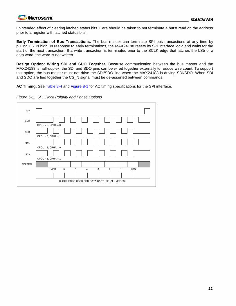
Clock Polarity and Phase. SCLK polarity and phase can be changed using the CPOL and CPHA pins. The CPOL pin defines the polarity of SCLK. When CPOL=0, SCLK is normally low and pulses high during bus transactions. When CPOL = 1, SCLK is normally high and pulses low during bus transactions. The CPHA pin sets the phase (active edge) of SCLK. When CPHA = 0, data is latched in on SDI on the leading edge of the SCLK pulse and updated on SDO on the trailing edge. When CPHA = 1, data is latched in on SDI on the trailing edge of the SCLK pulse and updated on SDO on the following leading edge. SCLK does not have to toggle between accesses, i.e., when CS_N is high. See Figure 5-1.
Device Selection. Normally each SPI device has its own chip-select line. The MAX24188 is selected when its CS_N pin is low. When CS_N is de-asserted the SDO signal is high impedance, and any incomplete transfer cycle is aborted. This behavior is asynchronous to the SCLK signal. The CS_N signal can stay asserted for the duration of multiple read and write cycles. The transition of CS_N from de-asserted to asserted defines the start of a cycle or multiple cycles.
Control Word. After CS_N is pulled low, the bus master transmits the control word during the first eight SCLK cycles. By default the 8-bit control word is sent with address MSb first: R/W A5 A4 A3 A2 A1 A0 BURST. When pin SPISWAP=1 the control word is sent with address LSb first: R/W A0 A1 A2 A3 A4 A5 BURST where A[5:0] is the register address, R/W is the data direction bit (1=read, 0=write), and BURST is the burst bit (1=burst access, 0=single-word access). In the discussion that follows, a control word with R/W = 1 is a read control word, while a control word with R/W = 0 is a write control word.
Data Word. By default, 16-bit data words are sent MSb first. When SPISWAP=1 data words are sent LSb first.
Single-Word Writes. See Figure 5-2. After CS_N goes low, the bus master transmits a write control word with BURST = 0 followed by the 16-bit word to be written. The data word is transferred to the register after the last data bit is sampled. If CS_N stays asserted the next word must be a control word.
Single-Word Reads. See Figure 5-2. After CS_N goes low, the bus master transmits a read control word with BURST = 0. The MAX24188 then responds with the requested 16-bit data word. When CS_N stays asserted the next word must be a control word.
Burst Writes. See Figure 5-2. After CS_N goes low, the bus master transmits a write control word with BURST = 1 followed by the first 16-bit data word to be written. The MAX24188 receives the first data word on SDI, writes it to the specified register, increments its internal address register, and prepares to receive the next data word. If the master continues to transmit, the MAX24188 continues to write the data received and increment its address counter. After the address counter reaches 1Fh it rolls over to address 00h and continues to increment. The bus master must terminate the transaction by pulling CS_N high after the last data word.
Burst Reads. See Figure 5-2. After CS_N goes low, the bus master transmits a read control word with BURST = 1. The MAX24188 then responds with the requested data word on SDO, increments its address counter, and prefetches the next data word. If the bus master continues to demand data, the MAX24188 continues to provide the data on SDO, increment its address counter, and prefetch the following word. After the address counter reaches 1Fh it rolls over to address 00h and continues to increment. The bus master must terminate the transaction by pulling CS_N high after the last data word. NOTE: The prefetch mentioned above can have the
_________________________________________________________________________________________________ MAX24188
11
unintended effect of clearing latched status bits. Care should be taken to not terminate a burst read on the address prior to a register with latched status bits.
Early Termination of Bus Transactions. The bus master can terminate SPI bus transactions at any time by pulling CS_N high. In response to early terminations, the MAX24188 resets its SPI interface logic and waits for the start of the next transaction. If a write transaction is terminated prior to the SCLK edge that latches the LSb of a data word, the word is not written.
Design Option: Wiring SDI and SDO Together. Because communication between the bus master and the MAX24188 is half-duplex, the SDI and SDO pins can be wired together externally to reduce wire count. To support this option, the bus master must not drive the SDI/SDO line when the MAX24188 is driving SDI/SDO. When SDI and SDO are tied together the CS_N signal must be de-asserted between commands.
AC Timing. See Table 8-4 and Figure 8-1 for AC timing specifications for the SPI interface.
Figure 5-1. SPI Clock Polarity and Phase Options
MSB LSB6 5 4 3 2 1
CS*
SCK
SCK
SCK
SCK
SDI/SDO
CLOCK EDGE USED FOR DATA CAPTURE (ALL MODES)
CPOL = 0, CPHA = 0
CPOL = 0, CPHA = 1
CPOL = 1, CPHA = 0
CPOL = 1, CPHA = 1

_________________________________________________________________________________________________ MAX24188
12
Figure 5-2. SPI Bus Transactions
5.4 Reference Clock PLL
The reference clock PLL (see block diagram in Figure 2-1) generates a 125MHz clock for the time engine and an eight-phase 125MHz clock for the output clock generator, programmable event generators and timestampers. The reference clock PLL locks to the REFCLK signal, which can be 125MHz, 25MHz, 12.8MHz or 10MHz as specified by the REF[1:0] pins during device reset. The 12.8MHz and 10MHz frequencies enable the device to share an oscillator with any clock synchronization ICs that may be on the same board.
A 125MHz clock from the reference clock PLL (locked to the REFCLK signal) can be output on one or more GPIO pins. See section 5.1 for configuration details.
If needed, the reference clock PLL can be powered down an bypassed by pulling the PLL_PWDN pin high. See section 5.2.2 for additional details.
R/ W Register Address Burst Data Word SDI
CS_N
SDO
Single-Word Write
Single-Word Read
R/ W Register Address Burst
Data Word
R/ W Register Address Burst Data Word 1
Burst Write
SDI
SDO
SDI
SDO
0 (Write) 0 (single)
1 (Read) 0 (single)
0 (Write) 1 (burst) Data Word N
R/ W Register Address Burst
Data Word 1
Burst Read
SDI 1 (Read) 1 (burst)
Data Word N SDO
CS_N
CS_N
CS_N
_________________________________________________________________________________________________ MAX24188
13
5.5 1588 Hardware
5.5.1 1588 Time Engine
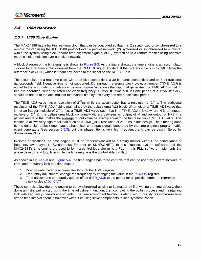
The MAX24188 has a built-in real-time clock that can be controlled so that it is (1) syntonized or synchronized to a remote master using the IEEE1588 protocol over a packet network, (2) syntonized or synchronized to a master within the system using clock and/or time alignment signals, or (3) syntonized to a remote master using adaptive mode circuit emulation over a packet network.
A block diagram of the time engine is shown in Figure 5-3. As the figure shows, the time engine is an accumulator clocked by a reference clock derived from the REFCLK signal. By default the reference clock is 125MHz from the reference clock PLL, which is frequency locked to the signal on the REFCLK pin.
The accumulator is a real-time clock with a 48-bit seconds field, a 30-bit nanoseconds field and an 8-bit fractional nanoseconds field. Negative time is not supported. During each reference clock cycle, a number (TIME_ADJ) is added to the accumulator to advance the time. Figure 5-4 shows the logic that generates the TIME_ADJ signal. In free-run operation, when the reference clock frequency is 125MHz, exactly 8.0ns (the period of a 125MHz clock) should be added to the accumulator to advance time by 8ns every 8ns reference clock period.
The TIME_ADJ value has a resolution of 2-32
ns while the accumulator has a resolution of 2-8
ns. The additional
resolution of the TIME_ADJ field is maintained by the delta-sigma () block. When given a TIME_ADJ value that
is not an integer multiple of 2-8
ns (i.e. a TIME_ADJ value such that N TIME_ADJ N+1 where N is an integer multiple of 2
-8ns), the delta-sigma block continually dithers between an output of N and an output of N+1 in a
pattern and ratio that makes the average output value be exactly equal to the full-resolution TIME_ADJ value. This technique allows very high resolution such as a TIME_ADJ resolution of 2^-32ns in this design. The dithering done by the delta-sigma block does cause phase jitter on output signals generated by the time engine's programmable event generators (see section 5.5.3), but this phase jitter is very high frequency and can be easily filtered by downstream PLLs.
In some applications the time engine must be frequency-locked to a timing master without the conveyance of frequency over layer 1 (Synchronous Ethernet or SDH/SONET). In this situation, system software and the MAX24188’s time engine are used to form a control loop similar to a PLL. In this PLL, software implements the phase detector and loop filter while the time engine is the controllable oscillator.
As shown in Figure 5-3 and Figure 5-4, the time engine has three controls that can be used by system software to time- and frequency-lock to a time master:
1. Directly write the time accumulator through the TIME register 2. Frequency adjustment: change the frequency by changing the value in the PERIOD register 3. Time adjustment: temporarily add an offset (PER_ADJ) to the period for a specific number of reference
clock cycles (ADJ_CNT)
These controls allow the time engine to be synchronized quickly to its master by first writing the time directly, then doing an initial pull-in step using the time adjustment function, then completing the pull-in process and maintaining lock with frequency (period) adjustments. The time adjustment function is also used to quickly resynchronize time after a time interval spent in holdover without causing slave components to lose synchronization.

_________________________________________________________________________________________________ MAX24188
14
Figure 5-3. 1588 Time Engine
-MAX
TIME_ADJ
NSEC
38 bits
SEC
48 bits
≥0
seconds
48 bits
ns fraction
32 bits
ns
8 bits
Time Formatns fraction
8 bits
nanoseconds
30 bits
125MHz Reference Clock
TIME register TIME register
unsigned integer 40 bits
1
0 Accumulator
nanoseconds
30 integer bits
8 fraction bits
2-8
ns resolution
Accumulator
Seconds
48 bits
Load Load
Increment
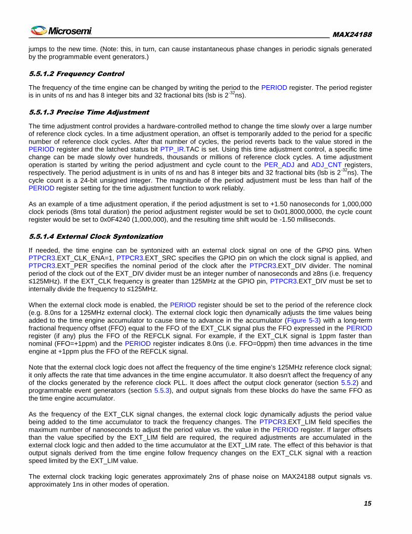
Figure 5-4. Time Engine Period Generator
ns fraction
32 bits
ns
8 bits
0
Down
Counter
¹0
1
0
EXT_CLK
EXT_PER
uint 8 bits
PERIOD
uint 40 bits
PER_ADJ
int 40 bits
ADJ_CNT
uint 24 bits
ADJ_LD
ns fraction
32 bits
ns
8 bits
ns
8 bits
ns fraction
32 bits
ns
8 bits
0
1
EXT_LIM
uint 2 bits
EXT_CLK_ENA
EXT_DIV
External Clock
Tracking Logic
TIME_ADJunsigned integer 40 bits
Load
5.5.1.1 Direct Time Write
The time engine accumulator can be written and read through the TIME register. The time is in 1588 standard format: 48 bits of seconds and 30 bits of nanoseconds. When such a write is done, the time engine instantaneously
_________________________________________________________________________________________________ MAX24188
15
jumps to the new time. (Note: this, in turn, can cause instantaneous phase changes in periodic signals generated by the programmable event generators.)
5.5.1.2 Frequency Control
The frequency of the time engine can be changed by writing the period to the PERIOD register. The period register is in units of ns and has 8 integer bits and 32 fractional bits (lsb is 2
-32ns).
5.5.1.3 Precise Time Adjustment
The time adjustment control provides a hardware-controlled method to change the time slowly over a large number of reference clock cycles. In a time adjustment operation, an offset is temporarily added to the period for a specific number of reference clock cycles. After that number of cycles, the period reverts back to the value stored in the PERIOD register and the latched status bit PTP_IR.TAC is set. Using this time adjustment control, a specific time change can be made slowly over hundreds, thousands or millions of reference clock cycles. A time adjustment operation is started by writing the period adjustment and cycle count to the PER_ADJ and ADJ_CNT registers, respectively. The period adjustment is in units of ns and has 8 integer bits and 32 fractional bits (lsb is 2
-32ns). The
cycle count is a 24-bit unsigned integer. The magnitude of the period adjustment must be less than half of the PERIOD register setting for the time adjustment function to work reliably.
As an example of a time adjustment operation, if the period adjustment is set to +1.50 nanoseconds for 1,000,000 clock periods (8ms total duration) the period adjustment register would be set to 0x01,8000,0000, the cycle count register would be set to 0x0F4240 (1,000,000), and the resulting time shift would be -1.50 milliseconds.
5.5.1.4 External Clock Syntonization
If needed, the time engine can be syntonized with an external clock signal on one of the GPIO pins. When PTPCR3.EXT_CLK_ENA=1, PTPCR3.EXT_SRC specifies the GPIO pin on which the clock signal is applied, and PTPCR3.EXT_PER specifies the nominal period of the clock after the PTPCR3.EXT_DIV divider. The nominal period of the clock out of the EXT_DIV divider must be an integer number of nanoseconds and ≥8ns (i.e. frequency ≤125MHz). If the EXT_CLK frequency is greater than 125MHz at the GPIO pin, PTPCR3.EXT_DIV must be set to internally divide the frequency to ≤125MHz.
When the external clock mode is enabled, the PERIOD register should be set to the period of the reference clock (e.g. 8.0ns for a 125MHz external clock). The external clock logic then dynamically adjusts the time values being added to the time engine accumulator to cause time to advance in the accumulator (Figure 5-3) with a long-term fractional frequency offset (FFO) equal to the FFO of the EXT_CLK signal plus the FFO expressed in the PERIOD register (if any) plus the FFO of the REFCLK signal. For example, if the EXT_CLK signal is 1ppm faster than nominal (FFO=+1ppm) and the PERIOD register indicates 8.0ns (i.e. FFO=0ppm) then time advances in the time engine at +1ppm plus the FFO of the REFCLK signal.
Note that the external clock logic does not affect the frequency of the time engine's 125MHz reference clock signal; it only affects the rate that time advances in the time engine accumulator. It also doesn't affect the frequency of any of the clocks generated by the reference clock PLL. It does affect the output clock generator (section 5.5.2) and programmable event generators (section 5.5.3), and output signals from these blocks do have the same FFO as the time engine accumulator.
As the frequency of the EXT_CLK signal changes, the external clock logic dynamically adjusts the period value being added to the time accumulator to track the frequency changes. The PTPCR3.EXT_LIM field specifies the maximum number of nanoseconds to adjust the period value vs. the value in the PERIOD register. If larger offsets than the value specified by the EXT_LIM field are required, the required adjustments are accumulated in the external clock logic and then added to the time accumulator at the EXT_LIM rate. The effect of this behavior is that output signals derived from the time engine follow frequency changes on the EXT_CLK signal with a reaction speed limited by the EXT_LIM value.
The external clock tracking logic generates approximately 2ns of phase noise on MAX24188 output signals vs. approximately 1ns in other modes of operation.

_________________________________________________________________________________________________ MAX24188
16
Note that another way to syntonize the time engine to a clock signal is to use the clock signal as MAX24188's REFCLK signal, since the time engine's reference clock is derived from the REFCLK signal.
5.5.2 Output Clock Generator
The primary frequency output from the 1588 time engine is the PTP_CLKO signal. PTP_CLKO can be configured
to be 125MHz n where n = 1 to 255 as set by PTPCR2.CLKO_DIV. Typical PTP_CLKO frequencies are 125MHz, 62.5MHz, 31.25MHz, 25MHz, 5MHz and 1MHz. PTP_CLKO can be inverted by setting PTPCR2.INV=1.
Whenever the 1588 time engine is synchronized to a time or frequency master, PTP_CLKO is, by extension, syntonized to the frequency of the master. Note that the frequency of PTP_CLKO is immediately affected by all 1588 time engine controls: direct time write, period adjustment, and time adjustment.
The output jitter of PTP_CLKO is approximately 1ns. To achieve this level of jitter when clocking the 1588 time engine with a 125MHz (8ns) reference clock, eight phases of the reference clock are used, effectively giving a 1GHz reference clock from which to synthesize PTP_CLKO.
PTP_CLKO can be made available on any of general-purpose I/O pins GPO2, GPIO2, or GPIO4-7 by configuring GPIOCR1 and/or GPIOCR2 appropriately.
5.5.3 Programmable Event Generators
The MAX24188 has two identical programmable event generators (PEGs). Each of these PEGs can be configured to generate output signals with time-triggered rising or falling edges. PEG output signals can be non-periodic control signals, 50% duty cycle clock signals, or periodic pulses, such as a one pulse per second (1PPS) signal. For each PEG, one or more GPIO pins must be configured using the appropriate field in GPIOCR1 or GPIOCR2 to output the PEG signal.
Each PEG has a controller that accepts commands written to a 22-bit-wide, 16-word-deep FIFO that stores multiple event generation commands. As shown in Table 5-4, bits 15:0 of each 22-bit word are a 16-bit time field or repeat count. Bits 19:16 are a command code (see Table 5-5). Bit 20 specifies GPIO pin behavior after the event: continue to drive or go high impedance. Bit 21 marks the event command as one for which the PEG controller must set the PTP_IR.P1EC or P2EC latched status bit when it has completed the command.
Table 5-4. PEG Command FIFO Fields
FIFO Bits Field Description
21 Stat When this bit is set, the PEG controller sets the P1EC or P2EC latched status bit after the event command is completed. This can be used, for example, to interrupt software on one-second boundaries.
20 Disable (After Event)
0 = Output pin continues to drive the last level (high or low) after the event 1 = Output pin goes high impedance one reference clock (8ns) after the event.
19:16 Command 4-bit event command code. See Table 5-5 for commands.
15:0 Data 16-bit data. See Table 5-5 for descriptions of what the data means for each command code.

_________________________________________________________________________________________________ MAX24188
17
Table 5-5. PEG Commands
FIFO[19:16]Command
Command Description
0000 Repeat. Let N=FIFO[3:0] and M=FIFO[15:4]. Repeat the last N FIFO entries M times. M=0 indicates repeat
forever (simple clock mode) until a new command is written to the PEG FIFO.
0001
Fractional Clock Synthesis Repeat. Let M1=FIFO[15:8] and M2=FIFO[7:0]. Repeat last 4 FIFO entries
forever. Two structures are possible here for the previous 4 FIFO entries: (1) Four 16-bit relative-time toggle commands (command=1111). Words 1 and 2 are repeated M1 times then words 3 and 4 are repeated M2 times. (2) Two 32-bit relative-time toggle commands (command=1110). The 32-bit command in words 1 and 2 is repeated 2*M1 times then the 32-bit command in words 3 and 4 is repeated 2*M2 times. In both cases the pattern is repeated forever until a new command is written to the PEG FIFO.
0010 Set Absolute Time Reference. Set the PEG’s absolute time reference point to the time engine’s current
time. The next relative time command will be relative to this reference point. FIFO[15:0] ignored.
0011 Undefined
01xx Create Positive Edge These three values of FIFO[19:18] are combined with the three values of FIFO[17:16]=01, 10 or 11 (described below) to create time-triggered edge placements in the PEG output signal.
10xx Create Negative Edge
11xx Toggle (Create Opposite Edge)
xx00 (xx¹00) Undefined
xx01 (xx¹00)
Absolute time value. First word of 5-word, 48-bit absolute time value.
FIFO[15:0]: Word 1 = seconds[47:32], word 2 = seconds[31:16], word 3 = seconds[15:0], word 4 = ns[29:16], word 5 = ns[15:0]. The command field (FIFO[19:16]) of words 2 through 5 is don’t-care (recommended value: same as word 1)
xx10 (xx¹00)
32-bit relative time value. First word of 2-word relative time value.
FIFO[15:0]: Word 1 = ns[29:16], word 2 =ns[15:0]. The command field (FIFO[19:16]) of word 2 is don’t-care (recommended value: same as word 1).
xx11 (xx¹00) 16-bit relative time value. Single-word relative time value, FIFO[15:0] is ns[15:0].
An absolute time command (xx01) or the Set Absolute Time Reference command (0010) must be used before relative time commands (xx10 or xx11) can be used. Relative commands create an event at a time relative to the previous event (the previous event can be absolute or relative).
When PEGCR.P1RES or P2RES is set to 1, the resolution of the 32-bit and 16-bit relative time values is increased by a factor of 256, giving a resolution of 1/256 (i.e. 2
-8) nanoseconds. This is used to generate a signal with a
period that is not an integer number of nanoseconds. The P1RES or P2RES bit must remain unchanged for the duration of a repeat or fractional synthesis repeat command.
The control bits PEGCR.P1RST and P2RST are used to reset the PEGs. When a PEG is reset, its command FIFO is emptied, its control logic is reset, and its output signal is driven low.
The control bits PEGCR.P1DIS and P2DIS prevent the PEG from moving to the next command in the PEG FIFO. When PnDIS=1, the PEG continues to execute any command or group of commands (grouped by repeat or fractional clock synthesis repeat commands) already being executed, but it cannot proceed to the next command until PnDIS is set to 0. This feature is valuable for ensuring that repeat groups are completely loaded into the FIFO before being executed by the PEG.
Real-time status bits PTP_SR.P1FF and P2FF indicate when the PEG command FIFOs are full. System software should monitor these bits to prevent FIFO overflow.
The PEG1 Command FIFO is written through the PEG1_FIFO register. The PEG2 Command FIFO is written through the PEG2_FIFO register.
The PEG Repeat command can be used to make periodic signals with periods that are integer multiples of 2ns (PEGCR.PnRES=0) or 2/256ns (PEGCR.PnRES=1). The basic idea is to first set an absolute reference and then repeat a toggle command at a relative time equal to half the period of the desired signal. As an example, to generate a 50% duty cycle 25MHz clock using PEG1, follow these steps:

_________________________________________________________________________________________________ MAX24188
18
1. Set PEGCR.P1DIS=1. 2. Write 0x20000 to the PEG1 FIFO (Set Absolute Time Reference command). 3. Write 0xF0014 to the PEG1 FIFO (Toggle command, 16-bit relative time, 20ns half cycle). 4. Write 0x00001 to the PEG1 FIFO (Repeat command, repeat previous 1 FIFO entry forever). 5. Set PEGCR.P1DIS=0.
As another example, to generate a one pulse per second (1PPS) signal with a 50ns wide pulse using PEG2, the basic idea is to first generate a rising edge at the next 1 second boundary (absolute time). Then repeat forever these two edge placements: a toggle command 50ns later followed by another toggle command 1 second minus 50ns later. Specifically, follow these steps:
1. Set PEGCR.P2DIS=1. 2. Write 0x50000 to the PEG2 FIFO (Create Positive Edge command, 48-bit absolute time, sec[47:32]) 3. Write 0x50000 to the PEG2 FIFO (sec[31:16] for above command) 4. Write 0x50000 to the PEG2 FIFO (sec[15:0] for above command) 5. Write 0x50000 to the PEG2 FIFO (ns[31:16] for above command) 6. Write 0x50000 to the PEG2 FIFO (ns[15:0] for above command) 7. Write 0xF0032 to the PEG2 FIFO (Toggle command, 16-bit relative time, 50ns) 8. Write 0xE3B9A to the PEG2 FIFO (Toggle command, 32-bit relative time, 999,999,950ns) 9. Write 0x0C9CE to the PEG2 FIFO (ns[15:0] for above command) 10. Write 0x00003 to the PEG2 FIFO (Repeat command, repeat previous 3 FIFO entries, i.e. the two
Toggle commands, forever) 11. Set PEGCR.P2DIS=0.
Note that in steps 2, 3 and 4 the seconds value would have to be set to a specific one-second period in the near future for the example to work correctly.
The PEG toggle and repeat commands for other common frequencies are shown in Table 5-6.
Table 5-6. Common Frequencies Using Repeat Command
Frequency
Toggle Command
Repeat Command PnRES bit
FIFO[19:16] Command
Half Period (ns) FIFO[15:0] Hex
1 Hz 0xE 500,000,000 0x1DCD 0x6500
0x00002 0
8 KHz 0xF 62,500 0xF424 0x00001 0
1MHz 0xF 500 0x01F4 0x00001 0
2.048MHz 0xF 62,500/256 0xF424 0x00001 1
10MHz 0xF 50 0x0032 0x00001 0
25MHz 0xF 20 0x0014 0x00001 0
The PEG Fractional Clock Synthesis Repeat command adds additional frequency capabilities. See the description of this command in Table 5-5. The generated jitter is minimized by the PEG internally repeating 1/16 of M1 then 1/16 of M2 in an alternating manner. This jitter is high frequency and therefore easily filtered by downstream PLLs. The numbers M1 and M2 are adhered to precisely to get an exact synthesis, even if M1 and M2 are not integer multiples of 16. The 1/256 resolution can be applied by setting PEGCR.P1RES or P2RES to 1 if needed.
Table 5-7 shows how to use the fractional clock synthesis repeat command to create common telecom frequencies (with P1RES or P2RES set to 1). FIFO Entries 1 through 4 are relative-time toggle commands.
Table 5-7. Common Frequencies Using Fractional Clock Synthesis Repeat Command
FREQ M1 M2 FIFO Entry 1 FIFO Entry 2 FIFO Entry 3 FIFO Entry 4
30.720MHz 1 2 16+ 70/256 ns 16+ 70/256 ns 16+ 71/256 ns 16+ 71/256 ns
19.440MHz 155 88 25 + 184/256ns 25 + 184/256ns 25 + 185/256ns 25 + 185/256ns
1.544MHz 86 107 323 + 213/256 ns (32-bit Command) 323 + 214/256 ns (32-bit Command)

_________________________________________________________________________________________________ MAX24188
19
Notes: The closest spacing of a relative edge to the previous event is 16ns (two 125MHz reference clock periods). Also, the highest frequency periodic signal that a PEG can produce is one fourth of the reference clock frequency (e.g. 31.25MHz for a 125MHz reference clock).
A PEG can also be used to encode a data value as a pulse of a specific width. A second device can then use input signal timestamping (section 5.5.4) to determine the width and decode the value. As an example, pulse width could be used to encode 8 bits of data per pulse using pulse_width =n*32 + 64 ns which creates pulse widths from 64ns to 8,224ns (255*32+64). Thirty-two bits of data can then be sent as four separate pulses. This method can be a useful way to convey the exact time at the one-second boundary from a time master to a time slave in the same system using the wire that already carries the 1 pulse per second signal or other time alignment signal.
5.5.4 Input Signal Timestamping
Any of the three timestampers in the MAX24188 (TS1, TS2 or TS3) can timestamp edges of an input signal (rising, falling or both). This feature can be used in a wide variety of applications to timestamp signals from sensors or other ICs in the system to note the precise time something important happens.
In addition, this feature can be used to time-align the MAX24188's time engine to another component in the system. This can be necessary, for instance, when the MAX24188 is a timestamper on one card in a multicard and/or multiport switch or router. Typically, such a system is required to perform as a 1588 boundary clock or transparent clock in which packets are timestamped at the MII interfaces of multiple ports. In such a system it is important that all the timestampers have a common understanding of the current time. The easiest, most accurate way to achieve this is to have each timestamper time-locked to a time alignment signal from a central 1588 clock.
Aligning the time engine to a time alignment signal involves these concepts:
Configure the source of the time alignment signal to output a signal with a rising or falling edge at an exact time boundary, such as a 1 pulse per second (1 PPS) signal that goes high at the start of each second.
Apply that signal to the MAX24188 on the GPIO pin specified by TSCR.TS1SRC_SEL (this example presumes the use of TS1). Also, configure the GPIO pin as an input by setting GPIOCR1.GPIOn_SEL=0.
Configure the timestamper to timestamp the significant edge of the time alignment signal (TSCR.TS1_EDGE=01 or 10).
System software then looks for an input signal timestamp by polling the MAX24188's real-time status bit PTP_SR.TS1_NE or waiting for an interrupt generated by latched status register PTP_IR.TS1_NE.
Software reads the timestamp from the FIFO as described in the TS1_FIFO register description.
Finally, software implements a PLL phase detector by calculating the difference between the timestamp and the expected value, implements the desired PLL loop filter behavior, and controls the time engine using any of the three controls described in section 5.5.1 (typically frequency/period).
This process is repeated continually for each significant edge of the input time alignment signal.
As shown in Table 6-2, when an input signal timestamp is read from a timestamp FIFO, bit 15 of TEIO5 indicates the polarity of the input signal edge: 0=falling, 1=rising.
Each timestamper has an eight entry FIFO. Software must be able to read timestamps out of the FIFO faster than the expected time alignment signal frequency to avoid FIFO overflow. Timestamper FIFO overflow is signaled by latched status bit PTP_IR.TSn_OF and can generate an interrupt if configured to do so. PTP_SR.TSn_NE provides real-time FIFO empty/not-empty status. A transition from FIFO empty to FIFO not-empty is signaled by latched status bit PTP_IR.TSn_NE, which can also generate an interrupt if configured.
_________________________________________________________________________________________________ MAX24188
20
For applications that need to use a timestamper to lock to an input clock signal, the signal going to the TS1 timestamper can be internally divided down by one or both of the TS1 dividers (configured by TS1_DIV1 and TSCR.TS1_DIV2. This frequency division reduces the number of edges that must be timestamped to avoid overflowing the timestamp FIFO.
The precision of input signal timestamps is 1ns (using eight phases of the 125MHz reference clock). The pulse width of the input time alignment signal can be very small (less than 10 ns) when only one edge is timestamped. When both edges are timestamped, it must be ≥24ns.
5.6 Power Supply Considerations
Due to the multi-power-supply nature of the device, some I/Os have parasitic diodes between a 1.2V supply and a 3.3V supply. When ramping power supplies up or down, care must be taken to avoid forward-biasing these diodes because it could cause latchup. Two methods are available to prevent this. The first method is to place a Schottky diode external to the device between the 1.2V supply and the 3.3V supply to force the 3.3V supply to be within one parasitic diode drop of the 1.2V supply. The second method is to ramp up the 3.3V supply first and then ramp up the 1.2V supply.

_________________________________________________________________________________________________ MAX24188
21
6. Register Descriptions
Addresses not listed in Table 6-1 below are should be written with 0x0000 and ignored when read.
6.1 Register Map
Table 6-1. Register Map
Addr Register Name R/W
0 ID RO
1 GPIOCR1 RW
2 GPIOCR2 RW
3 GPIOSR RO
4 PTP_IR RO
5 PTP_IE RW
6 PTP_SR RO
9 TEIO1 RW
10 TEIO2 RW
11 TEIO3 RW
12 TEIO4 RW
13 TEIO5 RW
14 TERW RW
16 PTPCR1 RW
17 PTPCR2 RW
18 TSCR RW
19 PEGCR RW
20 TS1_DIV RW
26 PTPCR3 RW
6.2 Direct Access Registers
The register operating type is described in the “R/W” column using the following codes:
Type Description
RW Read-Write. Register field can be written and read back.
RO Read Only. Register field can only be read; writing it has no effect. Write 0 for future compatibility.
SC Self Clearing. Register bit self clears to 0 after being written as 1
LH-E Latch High—Event. Bit latches high when the internal event occurs and returns low when it is read.
LL-E Latch Low—Event. Bit latches low when the internal event occurs and returns high when it is read.
In the register definitions below, the register addresses are provided at the end of the table title.
_________________________________________________________________________________________________ MAX24188
22
6.2.1 ID
The ID register matches the JTAG device ID (lower 12 bits) and revision (all 4 bits). Device ID Register (address: 0)
Bit(s) Name Description R/W Reset
15:12 REV REV[3:0] Device revision number. Contact factory for value. RO Note 1
11:0 DEVICE DEVICE[11:0] Device ID RO Note 1
Note 1: See Device Code in Table 7-2.
6.2.2 GPIOCR1
GPIO Control Register 1 (address: 1)
Bit(s) Name Description R/W Reset
15 RST Global device reset. See section 5.2.1. 0 = normal operation 1 = reset
RW, SC
0
14:12 GPO1_SEL[2:0] GPO1 output pin mode selection. See Table 5-1. RW 000
11:9 GPO2_SEL[2:0] GPO2 output pin mode selection. See Table 5-2. RW 000
8:6 GPIO1_SEL[2:0] GPIO1 output pin mode selection. See Table 5-1. RW Note 1
5:3 GPIO2_SEL[2:0] GPIO2 output pin mode selection. See Table 5-2. RW 000
2:0 GPIO3_SEL[2:0] GPIO3 output pin mode selection. See Table 5-1. RW 000 Note 1: At reset if GPO1 pin=1 the GPIO1_SEL bits are set to 100 (125MHz), else the bits are set to 000 (high impedance).
6.2.3 GPIOCR2
GPIO Control Register 2 (address: 2)
Bit(s) Name Description R/W Reset
15:14 Reserved Ignore on Read RO 0
13 GPIO47_LSC GPIO4-7 Latched Status Control. This bit controls the behavior of latched status bits GPIO4L through GPIO7L in GPIOSR. See section 5.1. 0 = Set latched status bit when input goes low 1 = Set latched status bit when input goes high
RW 0
12 GPIO13_LSC GPIO1-3 Latched Status Control. This bit controls the behavior of latched status bits GPIO1L through GPIO3L in GPIOSR. See section 5.1. 0 = Set latched status bit when input goes low 1 = Set latched status bit when input goes high
RW 0
11:9 GPIO7_SEL[2:0] GPIO7 output pin mode selection. See Table 5-3. RW 000
8:6 GPIO6_SEL[2:0] GPIO6 output pin mode selection. See Table 5-3. RW 000
5:3 GPIO5_SEL[2:0] GPIO5 output pin mode selection. See Table 5-3. RW 000
2:0 GPIO4_SEL[2:0] GPIO4 output pin mode selection. See Table 5-3. RW 000
_________________________________________________________________________________________________ MAX24188
23
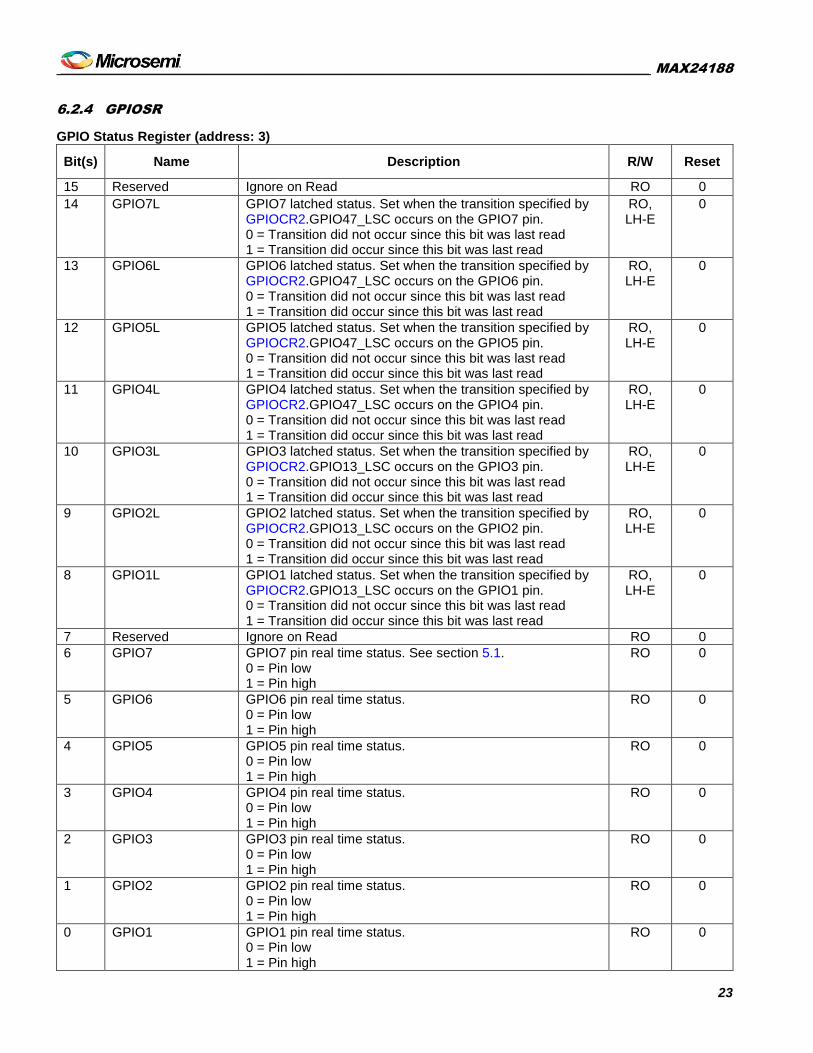
6.2.4 GPIOSR
GPIO Status Register (address: 3)
Bit(s) Name Description R/W Reset
15 Reserved Ignore on Read RO 0
14 GPIO7L GPIO7 latched status. Set when the transition specified by GPIOCR2.GPIO47_LSC occurs on the GPIO7 pin. 0 = Transition did not occur since this bit was last read 1 = Transition did occur since this bit was last read
RO, LH-E
0
13 GPIO6L GPIO6 latched status. Set when the transition specified by GPIOCR2.GPIO47_LSC occurs on the GPIO6 pin. 0 = Transition did not occur since this bit was last read 1 = Transition did occur since this bit was last read
RO, LH-E
0
12 GPIO5L GPIO5 latched status. Set when the transition specified by GPIOCR2.GPIO47_LSC occurs on the GPIO5 pin. 0 = Transition did not occur since this bit was last read 1 = Transition did occur since this bit was last read
RO, LH-E
0
11 GPIO4L GPIO4 latched status. Set when the transition specified by GPIOCR2.GPIO47_LSC occurs on the GPIO4 pin. 0 = Transition did not occur since this bit was last read 1 = Transition did occur since this bit was last read
RO, LH-E
0
10 GPIO3L GPIO3 latched status. Set when the transition specified by GPIOCR2.GPIO13_LSC occurs on the GPIO3 pin. 0 = Transition did not occur since this bit was last read 1 = Transition did occur since this bit was last read
RO, LH-E
0
9 GPIO2L GPIO2 latched status. Set when the transition specified by GPIOCR2.GPIO13_LSC occurs on the GPIO2 pin. 0 = Transition did not occur since this bit was last read 1 = Transition did occur since this bit was last read
RO, LH-E
0
8 GPIO1L GPIO1 latched status. Set when the transition specified by GPIOCR2.GPIO13_LSC occurs on the GPIO1 pin. 0 = Transition did not occur since this bit was last read 1 = Transition did occur since this bit was last read
RO, LH-E
0
7 Reserved Ignore on Read RO 0
6 GPIO7 GPIO7 pin real time status. See section 5.1. 0 = Pin low 1 = Pin high
RO 0
5 GPIO6 GPIO6 pin real time status. 0 = Pin low 1 = Pin high
RO 0
4 GPIO5 GPIO5 pin real time status. 0 = Pin low 1 = Pin high
RO 0
3 GPIO4 GPIO4 pin real time status. 0 = Pin low 1 = Pin high
RO 0
2 GPIO3 GPIO3 pin real time status. 0 = Pin low 1 = Pin high
RO 0
1 GPIO2 GPIO2 pin real time status. 0 = Pin low 1 = Pin high
RO 0
0 GPIO1 GPIO1 pin real time status. 0 = Pin low 1 = Pin high
RO 0

_________________________________________________________________________________________________ MAX24188
24
6.2.5 PTP_IR
When the latched status bit is set and the associated interrupt enable bit in PTP_IE is set an interrupt signal can be driven onto one of the GPIO pins by configuring the GPIOCR1 register.
PTP Interrupt Register (address: 4)
Bit(s) Name Description R/W Reset
15 Reserved Ignore on Read RO 0
14 PTP_IR Interrupt from this register. Set if any latched status and its associated enable bit are both set. See section 5.2.3. 0 = interrupt source not active 1 = interrupt source is active
RO 0
13 TS3_OF Timestamp 3 FIFO Overflow. Set when FIFO overflows. See section 5.5.4. 0 = No overflow occurred since last read 1 = Overflow occurred
RO, LH-E
0
12 TS3_NE Timestamp 3 FIFO Not Empty. Set when FIFO goes from empty to not empty. See section 5.5.4. 0 = No transition occurred since last read 1 = Empty-to-not-empty transition occurred
RO, LH-E
0
11 TS2_OF Timestamp 2 FIFO Overflow. Set when FIFO overflows. See section 5.5.4. 0 = No overflow occurred since last read 1 = Overflow occurred
RO, LH-E
0
10 TS2_NE Timestamp 2 FIFO Not Empty. Set when FIFO goes from empty to not empty. See section 5.5.4. 0 = No transition occurred since last read 1 = Empty-to-not-empty transition occurred
RO, LH-E
0
9 TS1_OF Timestamp 1 FIFO Overflow. Set when FIFO overflows. See section 5.5.4. 0 = No overflow occurred since last read 1 = Overflow occurred
RO, LH-E
0
8 TS1_NE Timestamp 1 FIFO Not Empty. Set when FIFO goes from empty to not empty. See section 5.5.4. 0 = No transition occurred since last read 1 = Empty-to-not-empty transition occurred
RO, LH-E
0
7 Reserved Ignore on Read RO 0
6 P2FNF PEG2 FIFO not full. See section 5.5.3. 0 = No transition occurred since last read 1 = Full-to-not-full transition occurred
RO, LH-E
0
5 P2SC PEG2 Sequence Complete. Set when a repeat sequence in the PEG2 controller is complete. See section 5.5.3. 0 = No repeat sequence completed since last read 1 = Repeat sequence completed since last read
RO, LH-E
0
4 P2EC PEG2 Event Complete. Set when a PEG2 event that is marked for status latching (PEG command FIFO bit 21=1) completes. See section 5.5.3. 0 = No marked event completed since last read 1 = Marked event completed since last read
RO, LH-E
0
3 P1FNF PEG1 FIFO not full. See section 5.5.3. 0 = No transition occurred since last read 1 = Full-to-not-full transition occurred
RO, LH-E
0
2 P1SC PEG1 Sequence Complete. Set when a repeat sequence in the PEG1 controller is complete. See section 5.5.3. 0 = No repeat sequence completed since last read
RO, LH-E
0
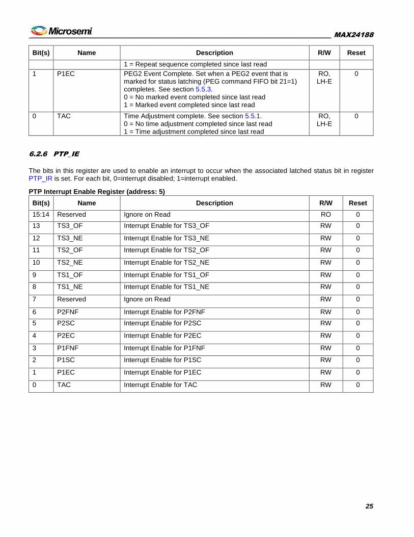
_________________________________________________________________________________________________ MAX24188
25
Bit(s) Name Description R/W Reset
1 = Repeat sequence completed since last read
1 P1EC PEG2 Event Complete. Set when a PEG2 event that is marked for status latching (PEG command FIFO bit 21=1) completes. See section 5.5.3. 0 = No marked event completed since last read 1 = Marked event completed since last read
RO, LH-E
0
0 TAC Time Adjustment complete. See section 5.5.1. 0 = No time adjustment completed since last read 1 = Time adjustment completed since last read
RO, LH-E
0
6.2.6 PTP_IE
The bits in this register are used to enable an interrupt to occur when the associated latched status bit in register PTP_IR is set. For each bit, 0=interrupt disabled; 1=interrupt enabled.
PTP Interrupt Enable Register (address: 5)
Bit(s) Name Description R/W Reset
15:14 Reserved Ignore on Read RO 0
13 TS3_OF Interrupt Enable for TS3_OF RW 0
12 TS3_NE Interrupt Enable for TS3_NE RW 0
11 TS2_OF Interrupt Enable for TS2_OF RW 0
10 TS2_NE Interrupt Enable for TS2_NE RW 0
9 TS1_OF Interrupt Enable for TS1_OF RW 0
8 TS1_NE Interrupt Enable for TS1_NE RW 0
7 Reserved Ignore on Read RW 0
6 P2FNF Interrupt Enable for P2FNF RW 0
5 P2SC Interrupt Enable for P2SC RW 0
4 P2EC Interrupt Enable for P2EC RW 0
3 P1FNF Interrupt Enable for P1FNF RW 0
2 P1SC Interrupt Enable for P1SC RW 0
1 P1EC Interrupt Enable for P1EC RW 0
0 TAC Interrupt Enable for TAC RW 0

_________________________________________________________________________________________________ MAX24188
26
6.2.7 PTP_SR
PTP Status Register (address: 6)
Bit(s) Name Description R/W Reset
15:10 Reserved Ignore on Read RO 0
9 TS3_NE Timestamp 3 FIFO not empty real time status. See section 5.5.4. 0 = Empty 1 = Not empty
RO 0
8 TS2_NE Timestamp 2 FIFO not empty real time status. See section 5.5.4. 0 = Empty 1 = Not empty
RO 0
7 TS1_NE Timestamp 1 FIFO not empty real time status. See section 5.5.4. 0 = Empty 1 = Not empty
RO 0
6 P2FF PEG2 control FIFO full/not-full real time status. See section 5.5.3. 0 = Not full 1 = Full
RO 0
5:4 Reserved Ignore on Read RO 0
3 P1FF PEG1 control FIFO full/not-full real time status. See section 5.5.3. 0 = Not full 1 = Full
RO 0
2:0 Reserved Ignore on Read RO 0
_________________________________________________________________________________________________ MAX24188
27
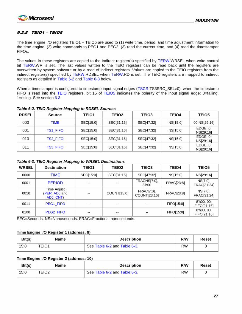
6.2.8 TEIO1 – TEIO5
The time engine I/O registers TEIO1 – TEIO5 are used to (1) write time, period, and time adjustment information to the time engine, (2) write commands to PEG1 and PEG2, (3) read the current time, and (4) read the timestamper FIFOs.
The values in these registers are copied to the indirect register(s) specified by TERW.WRSEL when write control bit TERW.WR is set. The last values written to the TEIO registers can be read back until the registers are overwritten by system software or by a read of indirect registers. Values are copied to the TEIO registers from the indirect register(s) specified by TERW.RDSEL when TERW.RD is set. The TEIO registers are mapped to indirect registers as detailed in Table 6-2 and Table 6-3 below.
When a timestamper is configured to timestamp input signal edges (TSCR.TS3SRC_SEL¹0), when the timestamp FIFO is read into the TEIO registers, bit 15 of TEIO5 indicates the polarity of the input signal edge: 0=falling, 1=rising. See section 6.3.
Table 6-2. TEIO Register Mapping to RDSEL Sources
RDSEL Source TEIO1 TEIO2 TEIO3 TEIO4 TEIO5
000 TIME SEC[15:0] SEC[31:16] SEC[47:32] NS[15:0] 00,NS[29:16]
001 TS1_FIFO SEC[15:0] SEC[31:16] SEC[47:32] NS[15:0] EDGE, 0, NS[29:16]
010 TS2_FIFO SEC[15:0] SEC[31:16] SEC[47:32] NS[15:0] EDGE, 0, NS[29:16]
011 TS3_FIFO SEC[15:0] SEC[31:16] SEC[47:32] NS[15:0] EDGE, 0, NS[29:16]
Table 6-3. TEIO Register Mapping to WRSEL Destinations
WRSEL Destination TEIO1 TEIO2 TEIO3 TEIO4 TEIO5
0000 TIME SEC[15:0] SEC[31:16] SEC[47:32] NS[15:0] NS[29:16]
0001 PERIOD -- -- FRACNS[7:0],
8'h00 FRAC[23:8]
NS[7:0], FRAC[31:24]
0010 Time Adjust
(PER_ADJ and ADJ_CNT)
-- COUNT[15:0] FRAC[7:0],
COUNT[23:16] FRAC[23:8]
NS[7:0], FRAC[31:24]
0011 PEG1_FIFO -- -- -- FIFO[15:0] 8'h00, 00,
FIFO[21:16]
0100 PEG2_FIFO -- -- -- FIFO[15:0] 8'h00, 00,
FIFO[21:16]
SEC=Seconds. NS=Nanoseconds. FRAC=Fractional nanoseconds. Time Engine I/O Register 1 (address: 9)
Bit(s) Name Description R/W Reset
15:0 TEIO1 See Table 6-2 and Table 6-3. RW 0
Time Engine I/O Register 2 (address: 10)
Bit(s) Name Description R/W Reset
15:0 TEIO2 See Table 6-2 and Table 6-3. RW 0

_________________________________________________________________________________________________ MAX24188
28
Time Engine I/O Register 3 (address: 11)
Bit(s) Name Description R/W Reset
15:0 TEIO3 See Table 6-2 and Table 6-3. RW 0
Time Engine I/O Register 4 (address: 12)
Bit(s) Name Description R/W Reset
15:0 TEIO4 See Table 6-2 and Table 6-3. RW 0
Time Engine I/O Register 5 (address: 13)
Bit(s) Name Description R/W Reset
15:0 TEIO5 See Table 6-2 and Table 6-3. RW 0
6.2.9 TERW
The TERW register is used to write the values of the TEIO registers into indirect registers as well as to read the values of indirect registers into the TEIO registers.
Read and write operations can be requested at the same time. When this is done the current TEIO register values are written to the register specified by WRSEL, and then the values of the registers specified by RDSEL are read into TEIO registers.
Time Engine Read/Write Register (address: 14)
Bit(s) Name Description R/W Reset
15 RD Set this bit to read the values of the indirect registers specified by RDSEL into the TEIO registers.
RW, SC
0
14:11 Reserved Ignore on Read RO 0
10:8 RDSEL[2:0] This field specifies the registers to be read into the TEIO registers when RD=1. See Table 6-2 for RDSEL decodes.
RW 0
7 WR Set this bit to write the values of the TEIO registers into the registers specified by WRSEL.
RW, SC
0
6:4 Reserved Ignore on Read RO 0
3:0 WRSEL[2:0] This field specifies the registers to be written from the TEIO registers when WR=1. See Table 6-3 for WRSEL decodes.
RW 0
Note: SC = self-clearing.

_________________________________________________________________________________________________ MAX24188
29
6.2.10 PTPCR1
PTP Control Register 1 (address: 16)
Bit(s) Name Description R/W Reset
15 TE_RST Time Engine Reset. This bit resets the logic of the 1588 time engine and related blocks. Self clearing. See section 5.2.1. 0 = normal operation 1 = reset
RW, SC
0
14 Reserved Ignore on read RW 1
13:12 Reserved Ignore on read RW 0
11:7 Reserved Ignore on read RO 0
6 Reserved Ignore on read RW 0
5 PLL_PWDN Reference Clock PLL Power Down. Setting this bit powers down and bypasses the reference clock PLL. See section 5.2.2. 0 = Power-down disabled 1 = Power-down enabled
RW 0
4:1 Reserved Ignore on Read RW 0
0 TE_PWDN Time Engine Power Down. Setting this bit disables clocks to the time engine, output clock generator, PEGs and timestampers. See section 5.2.2. 0 = Power-down disabled 1 = Power-down enabled
RW 0
6.2.11 PTPCR2
PTP Control Register 2 (address: 17)
Bit(s) Name Description R/W Reset
15:9 Reserved Ignore on Read RW 0
8 CLKO_INV PTP_CLKO Invert Control. See section 5.5.2. 0 = Non-inverted 1 = Inverted
RO 0
7:0 CLKO_DIV[7:0] Sets the PTP_CLKO output frequency by dividing 125MHz by CLKO_DIV which can be 1 to 255. When CLKO_DIV = 0 the output clock is disabled. See section 5.5.2.
RW
0

_________________________________________________________________________________________________ MAX24188
30
6.2.12 TSCR
Timestamp Control Register (address: 18)
Bit(s) Name Description R/W Reset
15:14 TS3_EDGE[1:0] Specifies which signal edge(s) should be timestamped by timestamper 3. When T3SRC_SEL=0 this field is ignored. See section 5.5.4. 00 = None 01 = Positive edge 10 = Negative edge 11 = Both edges
RW
0
13:12 TS3SRC_SEL[1:0] Specifies the source of the signal going to the TS3 timestamper. See section 5.5.4. 00 = None 01 = GPIO1 10 = GPIO2 11 = GPIO3
RW
0
11:10 TS2_EDGE[1:0] Specifies which signal edge(s) should be timestamped by timestamper 2. When T2SRC_SEL=0 this field is ignored. See section 5.5.4. 00 = None 01 = Positive edge 10 = Negative edge 11 = Both edges
RW
0
9:8 TS2SRC_SEL[1:0] Specifies the source of the signal going to the TS2 timestamper. See section 5.5.4. 00 = None 01 = GPIO1 10 = GPIO2 11 = GPIO3
RW
0
7:6 TS1_EDGE[1:0] Specifies which signal edge(s) should be timestamped by timestamper 1. 00 = None 01 = Positive edge 10 = Negative edge 11 = Both edges
RW
0
5:4 TS1SRC_SEL[1:0] Specifies the source of the signal going to the TS1 timestamper. The signal frequency is divided by the values specified by TS1_DIV1 and TSCR.TS1_DIV2 before going to the TS1 timestamper. See section 5.5.4.. 00 = PEG1 signal 01 = GPIO1 10 = GPIO2 11 = GPIO3
RW
0
3 Reserved Ignore on read RO 0
2:0 TS1_DIV2[2:0] Configures the second of two input signal dividers associated with timestamper 1.The second divider is configured by TS1_DIV1. See section 5.5.4. 000 = Do not divide 001 = Divide by 10 010 = Divide by 100 011 = Divide by 1000 100 = Divide by 2 101 = Divide by 80 110 = Divide by 800 111 = Divide by 8000
RW
0

_________________________________________________________________________________________________ MAX24188
31
6.2.13 PEGCR
PEG Control Register (address: 19)
Bit(s) Name Description R/W Reset
15:7 Reserved Ignore on read RO 0
6 P2RST A low-to-high transition of this bit causes programmable event generator 2 (PEG2) to reset. This empties the PEG2 command FIFO, resets the PEG2 control logic, and causes PEG2’s output signal to be driven low. See section 5.5.3.
RW
0
5 P2DIS PEG2 disable. This bit can be used to delay the processing of the commands written to the PEG2 FIFO. See section 5.5.3. 0 = enable processing new commands 1 = disable processing new commands
RW
0
4 P2RES PEG2 resolution. See section 5.5.3. 0 = 1 nanosecond resolution 1 = 1/256 nanosecond resolution
RW
0
3 Reserved Ignore on read RO 0
2 P1RST A low-to-high transition of this bit causes programmable event generator 1 (PEG1) to reset. This empties the PEG1 command FIFO, resets the PEG1 control logic, and causes PEG1’s output signal to be driven low. See section 5.5.3.
RW
0
1 P1DIS PEG1 disable. This bit can be used to delay the processing of the commands written to the PEG1 FIFO. See section 5.5.3. 0 = enable processing new commands 1 = disable processing new commands
RW
0
0 P1RES PEG1 resolution. See section 5.5.3. 0 = 1 nanosecond resolution 1 = 1/256 nanosecond resolution
RW
0
6.2.14 TS1_DIV1
Timestamper 1 Divider 1 Register (address: 20)
Bit(s) Name Description R/W Reset
15:0 TS1_DIV1[15:0] Configures the first of two input signal dividers associated with timestamper 1. TS1_DIV1=0 or 1 bypasses this divider (i.e. divide by 1). The second divider is configured by TSCR.TS1_DIV2. See section 5.5.4.
RW
0

_________________________________________________________________________________________________ MAX24188
32
6.2.15 PTPCR3
PTP Control Register 3 (address: 26)
Bit(s) Name Description R/W Reset
15:13 EXT_SRC[2:0] External clock source. When EXT_CLK_EN=1, this field specifies the source of EXT_CLK signal tracked by the 1588 time engine. See section 5.5.1.4. 000 = REFCLK pin 001 = GPIO1 pin 010 = GPIO2 pin 011 = GPIO3 pin 100 = GPIO4 pin 101 = GPIO5 pin 110 = GPIO6 pin 111 = GPIO7 pin
RW 0
12 EXT_CLK_EN External clock enable. See section 5.5.1.4. 0 = The rate at which time advances in the 1588 time engine
is controlled by the PERIOD register and the REFCLK signal
1 = The rate at which time advances in the 1588 time engine is controlled by the fractional frequency offset of the EXT_CLK signal.
RW 0
11:10 EXT_DIV[1:0] Set this bit to internally divide the EXT_CLK frequency. Must be non-zero for EXT_CLK frequencies >= 125MHz. See section 5.5.1.4. 00 = don't divide 01 = divide by 2 10 = divide by 4 11 = divide by 8
RW 0
9:8 EXT_LIM[1:0] Specifies the maximum number of nanoseconds to adjust the time engine accumulator period from the nominal value set by the PERIOD register. See section 5.5.1.4. 00 = 0.5ns 01 = 1ns 10 = 2ns 11 = 3ns
RW 0
7:0 EXT_PER[7:0] Specifies the nominal period, in integer nanoseconds, of the EXT_CLK signal AFTER the divider controlled by EXT_DIV. Examples 8 = 125MHz, 100 = 10MHz. See section 5.5.1.4.
RW 0
6.3 Indirect Registers
6.3.1 TIME
Format 48 bits of seconds, 30 bits of ns.
Read Access Write TERW with RD=1 and RDSEL=000 then read time from TEIO1 –TEIO5 as shown in Table 6-2.
Write Access Write time to TEIO1 – TEIO5 as shown in Table 6-3 and then write TERW with WR=1 and WRSEL=0000.
Description The time in the accumulator of the time engine can be written or read directly through this register. See section 5.5.1.

_________________________________________________________________________________________________ MAX24188
33
6.3.2 PERIOD
Format 8 bits of ns, 32 bits of fractional ns (i.e. 40 bits with lsb of 2-32
ns)
Read Access None
Write Access Write period to TEIO3 – TEIO5 as shown in Table 6-3 and then write TERW with WR=1 and WRSEL=0001.
Description The value in this register is added to the accumulator in the time engine every cycle of the 125MHz master clock. See Figure 5-3 and Figure 5-4. In free-run, period is set to exactly 8.0ns (0x08 0000 0000). When tracking a timing master, the period register is continually adjusted by system software as part of a hardware-software PLL. See section 5.5.1.
6.3.3 PER_ADJ
Format 8 bits of ns, 32 bits of fractional ns (i.e. 40 bits with lsb of 2-32
ns). 2s-complement.
Read Access None
Write Access Write period adjustment to TEIO3 – TEIO5 and write count to TEIO2 – TEIO3 as shown in Table 6-3 and then write TERW with WR=1 and WRSEL=0010.
Description To perform a precise time adjustment, both the PER_ADJ value and the PERIOD value are added to the accumulator in the time engine for the number of 125MHz master clock cycles specified in the ADJ_CNT register. This results in an exact time change equal to PER_ADJ * ADJ_CNT. See Figure 5-3 and Figure 5-4 in section 5.5.1.
6.3.4 ADJ_CNT
Format 24-bit unsigned integer
Read Access None
Write Access Write period adjustment to TEIO3 – TEIO5 and write count to TEIO2 – TEIO3 as shown in Table 6-3 and then write TERW with WR=1 and WRSEL=0010.
Description This register specifies the number of 125MHz master clock cycles that the PER_ADJ field should be added to the accumulator in the time engine. See the PER_ADJ register description for more details.
6.3.5 PEG1_FIFO, PEG2_FIFO
Format 22-bit FIFO command. See Table 5-4.
Read Access None
Write Access Write command to TEIO4 – TEIO5 as shown in Table 6-3 and then write TERW with WR=1 and WRSEL=0011 for PEG1 or WRSEL=0100 for PEG2.
Description Commands for the programmable event generators, PEG1 and PEG2, are written to the command FIFOs through these registers. See section 5.5.3.
6.3.6 TS1_FIFO, TS2_FIFO, TS3_FIFO
Format 48 bits of seconds, 30 bits of ns, 1 bit edge polarity.
Read Access Write TERW with RD=1 and RDSEL=001 for TS1_FIFO, RDSEL=010 for TS2_FIFO, or RDSEL=011 for TS3_FIFO then read timestamp from TEIO1 – TEIO5 as shown in Table 6-2.
Write Access None
Description Timestamps are read from the timestamp FIFOs through these registers. See section 5.5.4.

_________________________________________________________________________________________________ MAX24188
34
7. JTAG and Boundary Scan
7.1 JTAG Description
The MAX24188 supports the standard instruction codes SAMPLE/PRELOAD, BYPASS, and EXTEST. Optional public instructions included are HIGHZ, CLAMP, and IDCODE. Figure 7-1 shows a block diagram. The MAX24188 contains the following items, which meet the requirements set by the IEEE 1149.1 Standard Test Access Port and Boundary Scan Architecture:
Test Access Port (TAP) Bypass Register
TAP Controller Boundary Scan Register
Instruction Register Device Identification Register
The TAP has the necessary interface pins, namely JTCLK, JTRST_N, JTDI, JTDO, and JTMS. Details on these pins can be found in Table 4-4. Details about the boundary scan architecture and the TAP can be found in IEEE 1149.1-1990, IEEE 1149.1a-1993, and IEEE 1149.1b-1994.
Figure 7-1. JTAG Block Diagram
7.2 JTAG TAP Controller State Machine Description
This section discusses the operation of the TAP controller state machine. The TAP controller is a finite state machine that responds to the logic level at JTMS on the rising edge of JTCLK. Each of the states denoted in Figure 7-2 are described in the following paragraphs.
Test-Logic-Reset. Upon device power-up, the TAP controller starts in the Test-Logic-Reset state. The instruction register contains the IDCODE instruction. All system logic on the device operates normally.
Run-Test-Idle. Run-Test-Idle is used between scan operations or during specific tests. The instruction register and all test registers remain idle.
BOUNDARY SCAN
REGISTER
DEVICE IDENTIFICATION
REGISTER
BYPASS REGISTER
INSTRUCTION REGISTER
TEST ACCESS PORT CONTROLLER
MU
X
SELECT
ENABLE
JTDI
50k
JTMS
50k
JTCLK JTRST_N
50k
JTDO

_________________________________________________________________________________________________ MAX24188
35
Select-DR-Scan. All test registers retain their previous state. With JTMS low, a rising edge of JTCLK moves the controller into the Capture-DR state and initiates a scan sequence. JTMS high moves the controller to the Select-IR-SCAN state.
Capture-DR. Data can be parallel-loaded into the test register selected by the current instruction. If the instruction does not call for a parallel load or the selected test register does not allow parallel loads, the register remains at its current value. On the rising edge of JTCLK, the controller goes to the Shift-DR state if JTMS is low or to the Exit1-DR state if JTMS is high.
Shift-DR. The test register selected by the current instruction is connected between JTDI and JTDO and data is shifted one stage toward the serial output on each rising edge of JTCLK. If a test register selected by the current instruction is not placed in the serial path, it maintains its previous state.
Exit1-DR. While in this state, a rising edge on JTCLK with JTMS high puts the controller in the Update-DR state, which terminates the scanning process. A rising edge on JTCLK with JTMS low puts the controller in the Pause-DR state.
Pause-DR. Shifting of the test registers is halted while in this state. All test registers selected by the current instruction retain their previous state. The controller remains in this state while JTMS is low. A rising edge on JTCLK with JTMS high puts the controller in the Exit2-DR state.
Exit2-DR. While in this state, a rising edge on JTCLK with JTMS high puts the controller in the Update-DR state and terminates the scanning process. A rising edge on JTCLK with JTMS low puts the controller in the Shift-DR state.
Update-DR. A falling edge on JTCLK while in the Update-DR state latches the data from the shift register path of the test registers into the data output latches. This prevents changes at the parallel output because of changes in the shift register. A rising edge on JTCLK with JTMS low puts the controller in the Run-Test-Idle state. With JTMS high, the controller enters the Select-DR-Scan state.
Select-IR-Scan. All test registers retain their previous state. The instruction register remains unchanged during this state. With JTMS low, a rising edge on JTCLK moves the controller into the Capture-IR state and initiates a scan sequence for the instruction register. JTMS high during a rising edge on JTCLK puts the controller back into the Test-Logic-Reset state.
Capture-IR. The Capture-IR state is used to load the shift register in the instruction register with a fixed value. This value is loaded on the rising edge of JTCLK. If JTMS is high on the rising edge of JTCLK, the controller enters the Exit1-IR state. If JTMS is low on the rising edge of JTCLK, the controller enters the Shift-IR state.
Shift-IR. In this state, the instruction register’s shift register is connected between JTDI and JTDO and shifts data one stage for every rising edge of JTCLK toward the serial output. The parallel register and the test registers remain at their previous states. A rising edge on JTCLK with JTMS high moves the controller to the Exit1-IR state. A rising edge on JTCLK with JTMS low keeps the controller in the Shift-IR state, while moving data one stage through the instruction shift register.
Exit1-IR. A rising edge on JTCLK with JTMS low puts the controller in the Pause-IR state. If JTMS is high on the rising edge of JTCLK, the controller enters the Update-IR state and terminates the scanning process.
Pause-IR. Shifting of the instruction register is halted temporarily. With JTMS high, a rising edge on JTCLK puts the controller in the Exit2-IR state. The controller remains in the Pause-IR state if JTMS is low during a rising edge on JTCLK.
Exit2-IR. A rising edge on JTCLK with JTMS high puts the controller in the Update-IR state. The controller loops back to the Shift-IR state if JTMS is low during a rising edge of JTCLK in this state.
Update-IR. The instruction shifted into the instruction shift register is latched into the parallel output on the falling edge of JTCLK as the controller enters this state. Once latched, this instruction becomes the current instruction. A

_________________________________________________________________________________________________ MAX24188
36
rising edge on JTCLK with JTMS low puts the controller in the Run-Test-Idle state. With JTMS high, the controller enters the Select-DR-Scan state.
Figure 7-2. JTAG TAP Controller State Machine
7.3 JTAG Instruction Register and Instructions
The instruction register contains a shift register as well as a latched parallel output and is 3 bits in length. When the TAP controller enters the Shift-IR state, the instruction shift register is connected between JTDI and JTDO. While in the Shift-IR state, a rising edge on JTCLK with JTMS low shifts data one stage toward the serial output at JTDO. A rising edge on JTCLK in the Exit1-IR state or the Exit2-IR state with JTMS high moves the controller to the Update-IR state. The falling edge of that same JTCLK latches the data in the instruction shift register to the instruction parallel output. Table 7-1 shows the instructions supported by the MAX24188 and their respective operational binary codes.
Table 7-1. JTAG Instruction Codes
INSTRUCTIONS SELECTED REGISTER INSTRUCTION CODES
SAMPLE/PRELOAD Boundary Scan 010
BYPASS Bypass 111
EXTEST Boundary Scan 000
CLAMP Bypass 011
HIGHZ Bypass 100
IDCODE Device Identification 001
Test-Logic-Reset
Run-Test/Idle Select DR-Scan 1
0 Capture-DR 1
0 Shift-DR
0 1
Exit1- DR 1 0
Pause-DR 1
Exit2-DR 1
Update-DR 0
0
1
Select IR-Scan 1
0 Capture-IR
0 Shift-IR
0 1
Exit1-IR 1 0
Pause-IR 1
Exit2-IR 1
Update-IR 0
0
1
0 0
1 0
1 0 1

_________________________________________________________________________________________________ MAX24188
37
SAMPLE/PRELOAD. SAMPLE/RELOAD is a mandatory instruction for the IEEE 1149.1 specification. This instruction supports two functions. First, the digital I/Os of the device can be sampled at the boundary scan register, using the Capture-DR state, without interfering with the device’s normal operation. Second, data can be shifted into the boundary scan register through JTDI using the Shift-DR state.
EXTEST. EXTEST allows testing of the interconnections to the device. When the EXTEST instruction is latched in the instruction register, the following actions occur: (1) Once the EXTEST instruction is enabled through the Update-IR state, the parallel outputs of the digital output pins are driven. (2) The boundary scan register is connected between JTDI and JTDO. (3) The Capture-DR state samples all digital inputs into the boundary scan register.
BYPASS. When the BYPASS instruction is latched into the parallel instruction register, JTDI is connected to JTDO through the 1-bit bypass register. This allows data to pass from JTDI to JTDO without affecting the device’s normal operation.
IDCODE. When the IDCODE instruction is latched into the parallel instruction register, the device identification register is selected. The device ID code is loaded into the device identification register on the rising edge of JTCLK, following entry into the Capture-DR state. Shift-DR can be used to shift the ID code out serially through JTDO. During Test-Logic-Reset, the ID code is forced into the instruction register’s parallel output.
HIGHZ. All digital outputs are placed into a high-impedance state. The bypass register is connected between JTDI and JTDO.
CLAMP. All digital output pins output data from the boundary scan parallel output while connecting the bypass register between JTDI and JTDO. The outputs do not change during the CLAMP instruction.
7.4 JTAG Test Registers
IEEE 1149.1 requires a minimum of two test registers—the bypass register and the boundary scan register. An optional test register, the identification register, has been included in the device design. It is used with the IDCODE instruction and the Test-Logic-Reset state of the TAP controller.
Bypass Register. This is a single 1-bit shift register used with the BYPASS, CLAMP, and HIGHZ instructions to provide a short path between JTDI and JTDO.
Boundary Scan Register. This register contains a shift register path and a latched parallel output for control cells and digital I/O cells. BSDL files are available on the MAX24188 page of Microsemi’s website.
Identification Register. This register contains a 32-bit shift register and a 32-bit latched parallel output. It is selected during the IDCODE instruction and when the TAP controller is in the Test-Logic-Reset state. The device identification code for the MAX24188 is shown in Table 7-2.
Table 7-2. JTAG ID Code
DEVICE REVISION DEVICE CODE MANUFACTURER CODE REQUIRED
MAX24188 Note 1 0101 1110 0111 1100 00010100001 1
Note 1: 0000 = rev A1. 0001 = rev B1. Other values: contact factory.

_________________________________________________________________________________________________ MAX24188
38
8. Electrical Characteristics
ABSOLUTE MAXIMUM RATINGS
Voltage Range on Any Signal IO Lead with Respect to VSS .................................................................. -0.3V to +5.5V Supply Voltage (VDD12) Range with Respect to VSS ........................................................................ -0.3V to +1.32V Supply Voltage (VDD33) Range with Respect to VSS ......................................................................... -0.3V to +3.63V Operating Temperature Range: Industrial ............................................................................................ -40°C to +85°C Storage Temperature Range ............................................................................................................... -55°C to +125°C
Lead Temperature (soldering, 10s) .................................................................................................................... +300C Soldering Temperature (reflow) ......................................................................................................................... +260°C Stresses beyond those listed under “Absolute Maximum Ratings” may cause permanent damage to the device. These are stress ratings only, and functional operation of the device at these or any other conditions beyond those indicated in the operational sections of the specifications is not implied. Exposure to the absolute maximum rating conditions for extended periods may affect device. Ambient operating temperature range when device is mounted on a four-layer JEDEC test board with no airflow. Note 1: The typical values listed in the tables of section 8 are not production tested.
Note 2: Specifications to -40C are guaranteed by design and not production tested.
8.1 Recommended Operating Conditions
Table 8-1. Recommended DC Operating Conditions
PARAMETER SYMBOL CONDITIONS MIN TYP MAX UNITS
Supply Voltage, Nominal 1.2V VDD12 1.14 1.2 1.26 V
Supply Voltage, Nominal 3.3V VDD33 3.135 3.3 3.465 V
Ambient Temperature Range TA -40 +85 °C
Junction Temperature Range TJ -40 +125 °C
8.2 DC Electrical Characteristics
Unless otherwise stated, all specifications in this section are valid for VDD12 = 1.2V 5%, VDD33 = 3.3V 5% and TA = -40°C to +85°C.
Table 8-2. DC Characteristics
PARAMETER SYMBOL CONDITIONS MIN TYP MAX UNITS
Supply Current, VDD12 Pins IDD12 10, 25 or 125MHz REFCLK
85 mA
Supply Current, VDD33 Pins IDD33 110 mA
Supply Current, VDD12 Pins IDD12 12.8MHz REFCLK (Note 1)
100 125 mA
Supply Current, VDD33 Pins IDD33 135 160 mA
Supply Current, VDD12 Pins IDD12 PLL_PWDN=1, fREF = freq. of REFCLK in MHz
0.23*fREF+1 mA
Supply Current, VDD33 Pins IDD33 PLL_PWDN=1, all GPIO configured as inputs or disabled, fREF = freq. of REFCLK in MHz
0.47*fREF+20 mA
Supply Current Reduction, Time Engine Power-down, VDD12
IDDTE12 PTPCR1.TE_PWDN=1 20 mA
Supply Current, Full Power-down, VDD12
IDDPD12 PLL_PWDN=1, REFCLK stopped
2 mA
Supply Current, Full Power-down, VDD33
IDDPD33 20 mA
Input Capacitance CIN 4 pF
Output Capacitance COUT 7 pF
Note 1:
When a 12.8MHz oscillator is used the reference clock PLL uses a two-stage process to perform the frequency conversion and therefore consumes additional power.

_________________________________________________________________________________________________ MAX24188
39
8.2.1 CMOS/TTL DC Characteristics
Table 8-3. DC Characteristics
PARAMETER SYMBOL CONDITIONS MIN TYP MAX UNITS
Output High Voltage VOH IOH = -1mA, VDD=3.135V 2.4 5.5 V
Output Low Voltage VOL IOL = 1mA, VDD=3.135V 0 0.4 V
Input High Voltage VIH 2.0 VDD+0.2V V
Input Low Voltage VIL -0.2 0.8 V
Input High Current IIH VIN=3.3V 10 A
Input Low Current IIL VIN=0V -10 A
Output and I/O Leakage (when High Impedance)
ILO
-10 +10 A
8.3 AC Electrical Characteristics
Unless otherwise stated, all specifications in this section are valid for VDD12 = 1.2V 5%, VDD33 = 3.3V 5% and TA = -40°C to +85°C.
8.3.1 SPI Interface AC Characteristics
Table 8-4. SPI Interface Timing
PARAMETER (Note 1) (Note 2) SYMBOL MIN TYP MAX UNITS
SCLK Frequency fBUS 25 MHz
SCLK Cycle Time tCYC 40 ns
CS_N Setup to First SCLK Edge tSUC 5 ns
CS_N Hold Time After Last SCLK Edge tHDC 5 ns
SCLK High Time tCLKH 15 ns
SCLK Low Time tCLKL 15 ns
SDI Data Setup Time tSUI 5 ns
SDI Data Hold Time tHDI 5 ns
SDO Enable Time (High-Impedance to Output Active) (Note 4) tEN 5 15 ns
SDO Disable Time (Output Active to High-Impedance) tDIS 15 ns
SDO Data Valid Time (Note 3) tDV 5 16 ns
Note 1: Note 2: Note 3: Note 4:
All timing is specified with 100pF load on all SPI pins. All specifications in this table are guaranteed by design. Data is valid on SDO until min delay time. SDO is high impedance for at least min enable time.

_________________________________________________________________________________________________ MAX24188
40
Figure 8-1. SPI Interface Timing Diagram
CS
SCLK,
CPOL=0
SCLK,
CPOL=1
tSUI
tHDI
SDI
tCYC
tSUC
tCLKH
tCLKL
tCLKL
tCLKH
tHDC
SDO
tEN
tDV
tHDO
tDIS
CPHA = 0
CPHA = 1
CS
SCLK,
CPOL=0
SCLK,
CPOL=1
tCYC
tSUC
tCLKH
tCLKL
tCLKL
tHDC
tSUI
tHDI
SDI
SDO
tEN
tDV
tHDO
tDIS
tCLKH

_________________________________________________________________________________________________ MAX24188
41
8.3.2 JTAG Interface AC Characteristics
Table 8-5. JTAG Interface Timing
PARAMETER (Note 2) SYMBOL MIN TYP MAX UNITS
JTCLK Clock Period t1 1000 ns
JTCLK Clock High/Low Time (Note 1) t2/t3 50 500 ns
JTCLK to JTDI, JTMS Setup Time t4 50 ns
JTCLK to JTDI, JTMS Hold Time t5 50 ns
JTCLK to JTDO Delay t6 2 50 ns
JTCLK to JTDO High-Impedance Delay t7 50 ns
JTRST_N Width Low Time t8 100 ns
Note 1: Note 2:
Clock can be stopped high or low. All specifications in this table are guaranteed by design.
Figure 8-2. JTAG Timing Diagram
t1 EGISTER
JTDO
t4
t5
t2 R
DD
V
D
Rev: MMDDYY
TEST ACCESS PORT
e
v:
t3 TEST ACCESS PORT
D
DYY
TEST ACCESS PORT
t7 CONTROTEST ACCESS PORT
T
JTDI, JTMS
TEST ACCESS PORT
EST ACCESS PORT
t6
t8
8 CONTROLLER
JTCLK
JTRST_N
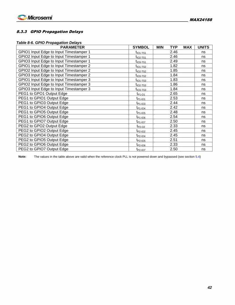
_________________________________________________________________________________________________ MAX24188
42
8.3.3 GPIO Propagation Delays
Table 8-6. GPIO Propagation Delays
PARAMETER SYMBOL MIN TYP MAX UNITS
GPIO1 Input Edge to Input Timestamper 1 tIO1-TS1 2.46 ns
GPIO2 Input Edge to Input Timestamper 1 tIO2-TS1 2.46 ns
GPIO3 Input Edge to Input Timestamper 1 tIO3-TS1 2.49 ns
GPIO1 Input Edge to Input Timestamper 2 tIO1-TS2 1.82 ns
GPIO2 Input Edge to Input Timestamper 2 tIO2-TS2 1.85 ns
GPIO3 Input Edge to Input Timestamper 2 tIO3-TS2 1.84 ns
GPIO1 Input Edge to Input Timestamper 3 tIO1-TS3 1.83 ns
GPIO2 Input Edge to Input Timestamper 3 tIO2-TS3 1.86 ns
GPIO3 Input Edge to Input Timestamper 3 tIO3-TS3 1.84 ns
PEG1 to GPO1 Output Edge tP1-O1 2.65 ns
PEG1 to GPIO1 Output Edge tP1-IO1 2.53 ns
PEG1 to GPIO3 Output Edge tP1-IO3 2.44 ns
PEG1 to GPIO4 Output Edge tP1-IO4 2.42 ns
PEG1 to GPIO5 Output Edge tP1-IO5 2.48 ns
PEG1 to GPIO6 Output Edge tP1-IO6 2.54 ns
PEG1 to GPIO7 Output Edge tP1-IO7 2.50 ns
PEG2 to GPO2 Output Edge tP2-O2 2.33 ns
PEG2 to GPIO2 Output Edge tP2-IO2 2.45 ns
PEG2 to GPIO4 Output Edge tP2-IO4 2.45 ns
PEG2 to GPIO5 Output Edge tP2-IO5 2.51 ns
PEG2 to GPIO6 Output Edge tP2-IO6 2.33 ns
PEG2 to GPIO7 Output Edge tP2-IO7 2.50 ns
Note: The values in the table above are valid when the reference clock PLL is not powered down and bypassed (see section 5.4)
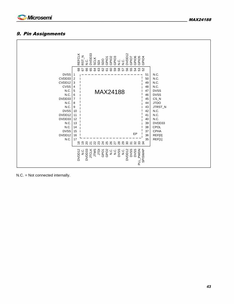
_________________________________________________________________________________________________ MAX24188
43
9. Pin Assignments
DVSS
CVDD33R
EF
CL
K
RS
T_
N
N.C
.
SC
LK
SD
I
DV
DD
33
SD
O
GP
IO1
GP
IO2
GP
IO3
N.C
.
N.C
.
DV
DD
12
GP
IO7
GP
IO6
GP
IO5
GP
IO4
CVDD12
CVSS
N.C.
N.C.
DVDD33
N.C.
N.C.
DVSS
DVDD12
DVDD33
N.C.
N.C.
DVSS
DVDD12
1
2
3
4
5
6
7
8
9
10
11
12
13
14
15
16
N.C. 17
68
67
66
65
64
63
62
61
60
59
58
57
56
55
54
53
52
N.C.
N.C.
N.C.
N.C.
DVSS
DVSS
CS_N
JTDO
JTRST_N
N.C.
N.C.
N.C.
DVDD33
CPOL
CPHA
REF[0]
REF[1]
51
50
49
48
47
46
45
44
43
42
41
40
39
38
37
36
35
DV
DD
12
N.C
.
DV
DD
33
JT
CL
K
JT
MS
JT
DI
GP
O1
GP
O2
N.C
.
N.C
.
DV
SS
N.C
.
DV
DD
12
DV
SS
DV
SS
PL
L_
PW
DN
SP
ISW
AP
18
19
20
21
22
23
24
25
26
27
28
29
30
31
32
33
34
EP
MAX24188
N.C. = Not connected internally.

_________________________________________________________________________________________________ MAX24188
44
10. Package and Thermal Information
Note: The exposed pad (EP) on the bottom of this package must be connected to the ground plane. EP also functions as a heatsink. Solder to the circuit-board ground plane to achieve the thermal specifications listed below.
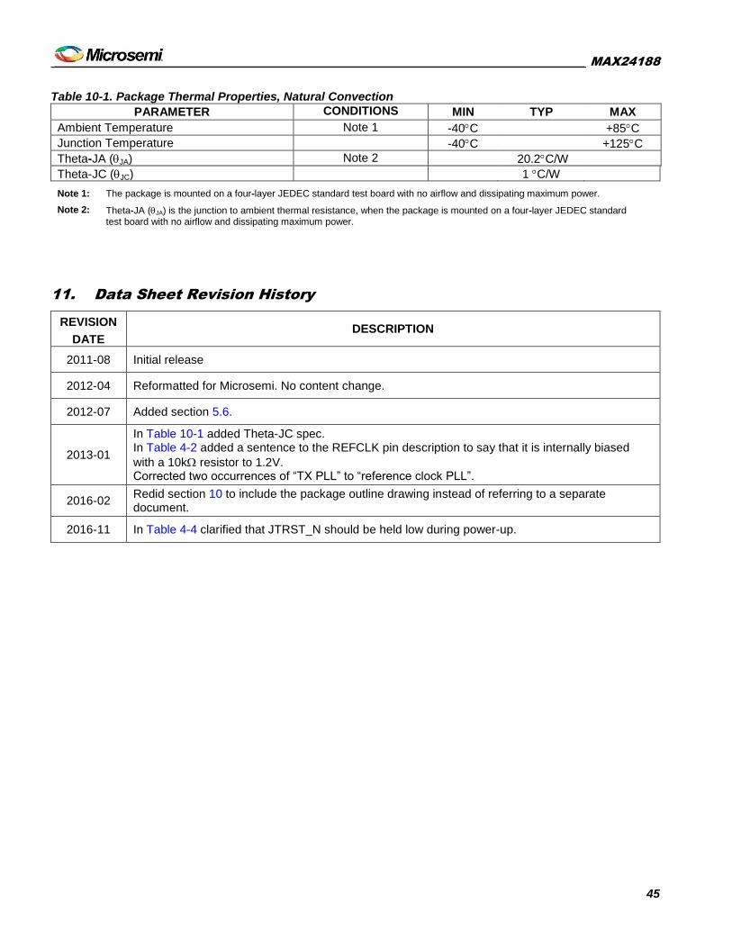
_________________________________________________________________________________________________ MAX24188
45
Table 10-1. Package Thermal Properties, Natural Convection
PARAMETER CONDITIONS MIN TYP MAX
Ambient Temperature
Note 1 -40C +85C
Junction Temperature -40C +125C
Theta-JA (JA) Note 2 20.2C/W
Theta-JC (JC) 1 C/W
Note 1: The package is mounted on a four-layer JEDEC standard test board with no airflow and dissipating maximum power.
Note 2: Theta-JA (JA) is the junction to ambient thermal resistance, when the package is mounted on a four-layer JEDEC standard test board with no airflow and dissipating maximum power.
11. Data Sheet Revision History
REVISION
DATE DESCRIPTION
2011-08 Initial release
2012-04 Reformatted for Microsemi. No content change.
2012-07 Added section 5.6.
2013-01
In Table 10-1 added Theta-JC spec. In Table 4-2 added a sentence to the REFCLK pin description to say that it is internally biased
with a 10k resistor to 1.2V. Corrected two occurrences of “TX PLL” to “reference clock PLL”.
2016-02 Redid section 10 to include the package outline drawing instead of referring to a separate document.
2016-11 In Table 4-4 clarified that JTRST_N should be held low during power-up.

Microsemi Corporation (Nasdaq: MSCC) offers a comprehensive portfolio of semiconductor
and system solutions for communications, defense & security, aerospace and industrial
markets. Products include high-performance and radiation-hardened analog mixed-signal
integrated circuits, FPGAs, SoCs and ASICs; power management products; timing and
synchronization devices and precise time solutions, setting the world’s standard for time; voice
processing devices; RF solutions; discrete components; security technologies and scalable
anti-tamper products; Power-over-Ethernet ICs and midspans; as well as custom design
capabilities and services. Microsemi is headquartered in Aliso Viejo, Calif., and has
approximately 3,400 employees globally. Learn more at www.microsemi.com.
© 2016 Microsemi Corporation. All rights reserved. Microsemi and the Microsemi logo are trademarks of Microsemi Corporation. All other trademarks and service marks are the property of their respective owners.
Microsemi Corporate Headquarters One Enterprise, Aliso Viejo, CA 92656 USA Within the USA: +1 (800) 713-4113 Outside the USA: +1 (949) 380-6100 Sales: +1 (949) 380-6136 Fax: +1 (949) 215-4996
E-mail: [email protected]
Microsemi makes no warranty, representation, or guarantee regarding the information contained herein or
the suitability of its products and services for any particular purpose, nor does Microsemi assume any
liability whatsoever arising out of the application or use of any product or circuit. The products sold
hereunder and any other products sold by Microsemi have been subject to limited testing and should not
be used in conjunction with mission-critical equipment or applications. Any performance specifications are
believed to be reliable but are not verified, and Buyer must conduct and complete all performance and
other testing of the products, alone and together with, or installed in, any end-products. Buyer shall not
rely on any data and performance specifications or parameters provided by Microsemi. It is the Buyer’s
responsibility to independently determine suitability of any products and to test and verify the same. The
information provided by Microsemi hereunder is provided “as is, where is” and with all faults, and the
entire risk associated with such information is entirely with the Buyer. Microsemi does not grant, explicitly
or implicitly, to any party any patent rights, licenses, or any other IP rights, whether with regard to such
information itself or anything described by such information. Information provided in this document is
proprietary to Microsemi, and Microsemi reserves the right to make any changes to the information in this
document or to any products and services at any time without notice.