Embed Size (px)
Citation preview

AFBR-79EBPZBi-Directional, QSFP+ Pluggable, Duplex LC40 Gigabit Ethernet Fiber-Optics Transceiver
Data Sheet
Patent - www.avagotech.com/patents
DescriptionThe Avago Technologies AFBR-79EBPZ is a Four-Channel, Pluggable, LC Duplex, Fiber-Optic QSFP+ Transceiver for 40 Gigabit Ethernet Applications. This transceiver is a high performance module for short-range duplex data com-munication and interconnect applications. It integrates four electrical data lanes in each direction into transmis-sion over a single LC duplex fiber optic cable. Each elec-trical lane operates at 10.3125 Gbps and conforms to the 40GE XLPPI interface.
The AFBR-79EBPZ transceiver internally multiplexes an XLPPI 4x10G interface into two 20Gb/s electrical chan-nels, transmitting and receiving each optically over one simplex LC fiber using bi-directional optics. This results in an aggregate bandwidth of 40Gbps into a duplex LC cable. This allows reuse of the installed LC duplex cabling infrastructure for 40GbE application.
Link distances up to 100 m using OM3 and 150m using OM4 optical fiber are supported. These modules are de-signed to operate over multimode fiber systems using a nominal wavelength of 850nm on one end and 900nm on the other end. The electrical interface uses a 38 contact QSFP+ type edge connector. The optical interface uses a conventional LC duplex connector. This module incorpo-rates Avago Technologies proven integrated circuit and VCSEL technology to provide reliable long life, high per-formance, and consistent service.
Part Number Ordering Options
40 Gigabit Ethernet Transceiver AFBR-79EBPZ
40 Gigabit Ethernet Receiver AFBR-79EBRZ
Evaluation Kit* AFBR-79Q4EKZ
*Includes GUI and User Guide
Features• Compliant to the 40GbE XLPPI electrical specification
per IEEE 802.3ba-2010
• Compliant to QSFP+ SFF-8436 Specification
• Power Level 4: Max Power 3.5W
• Class 1M Eye Safety
• High port density: 21mm horizontal port pitch
• Operates at 10.3125 Gbps per electrical channel with 64b/66b encoded data
• Links up to 100m using OM3 and 150m using OM4 optical fiber
• +10 to +70ºC case temperature operating range
• Proven High Reliability technology: Avago VCSEL transmitters and Avago PIN receiver
• Hot pluggable transceiver for ease of installation and servicing
• Two wire Serial (TWS) Management Interface with maskable interrupts for expanded functionality
• Utilizes a standard LC duplex fiber cable allowing reuse of existing cable infrastructure
Applications• 40 Gigabit Ethernet interconnects
• Datacom/Telecom switch & router connections
• Data aggregation and backplane applications
• Proprietary protocol and density applications

2
Figure 1. Transceiver Block Diagram
Transmitter The optical transmitter portion of the transceiver (see Fig-ure 1) incorporates a 4-channel XLPPI input buffer, elec-trical multiplexer, two laser drivers and two high speed VCSELs (Vertical Cavity Surface Emitting Laser). The trans-mitter is designed for EN 60825 and CDRH Class 1M eye safety compliance. The Tx Input Buffer provides XLPPI compatible differential inputs presenting a nominal dif-ferential input impedance of 100 Ohms. AC coupling capacitors are located inside the QSFP+ module and are not required on the host board. For module control and interrogation, the control interface (LVTTL compatible) in-corporates a Two Wire Serial (TWS) interface of clock and data signals.
ReceiverThe optical receiver portion of the transceiver (see Figure 1) incorporates two high speed PIN photodiodes, TIAs, signal processors, electrical de-multiplexer and 4 chan-nel electrical output buffer blocks. The Rx Output Buffer provides XLPPI compatible differential outputs for the high speed electrical interface presenting nominal single-ended output impedances of 50 Ohms to AC ground and 100 Ohms differentially that should be differentially termi-nated with 100 Ohms. AC coupling capacitors are located inside the QSFP+ module and are not required on the host board.
The electrical output will squelch for loss of input signal (unless squelch is disabled) and channel de-activation through TWS interface. To reduce the need for polling, a hardware interrupt signal INTL is provided to inform hosts of an assertion of LOS or Tx_FAULT.
WARNING
CLASS 1M LASER PRODUCT: INVISIBLE LASER RADIATION, DO NOT VIEW DIRECTLY WITH OPTICAL INSTRUMENTS
CAUTION! Viewing the laser output with certain optical instruments (for example, eye loupes, magnifiers and microscopes) within a distance of 100 mm may pose an eye hazard.
CAUTION! Use of controls or adjustments or performance of procedures other than those specified herein may result in hazardous radiation exposure.
Note: Standard used for classification: EN 60825-1:2007
INVISIBLE LASER RADIATIONDO NOT VIEW DIRECTLY
WITH OPTICAL INSTRUMENTSCLASS 1M LASER PRODUCT
40GE XLPPI Electrical Interface
Din[3:0][p/n] (8)
Dout[3:0][p/n] (8)
SCLSDA
Mod SelLPMode
ModPresLResetL
IntL
20G BiDi Optical
20G BiDi Optical20G
QSFP ElectricalConnector
Gearbox IC
uC
LC Duplex Optical Interface
20G Laser Driver + TIA
20G VCSEL, PIN and Bidirectional optics
TX λ1
RX λ2
20G VCSEL, PIN and Bidirectional optics
TX λ2
RX λ1
20G Laser Driver + TIA
20G
20G
4X10G CDR
2X20GCDR2:4 DeMux
4:2 Mux 20G
3
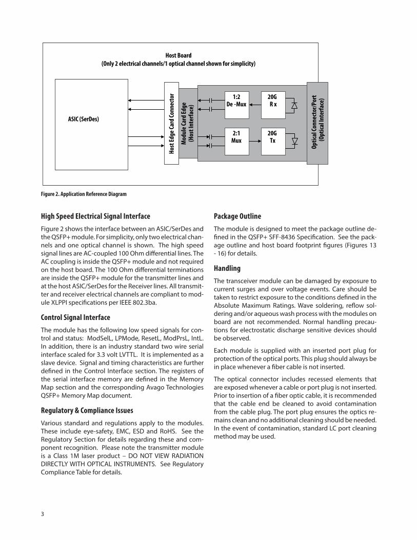
High Speed Electrical Signal InterfaceFigure 2 shows the interface between an ASIC/SerDes and the QSFP+ module. For simplicity, only two electrical chan-nels and one optical channel is shown. The high speed signal lines are AC-coupled 100 Ohm differential lines. The AC coupling is inside the QSFP+ module and not required on the host board. The 100 Ohm differential terminations are inside the QSFP+ module for the transmitter lines and at the host ASIC/SerDes for the Receiver lines. All transmit-ter and receiver electrical channels are compliant to mod-ule XLPPI specifications per IEEE 802.3ba.
Control Signal InterfaceThe module has the following low speed signals for con-trol and status: ModSelL, LPMode, ResetL, ModPrsL, IntL. In addition, there is an industry standard two wire serial interface scaled for 3.3 volt LVTTL. It is implemented as a slave device. Signal and timing characteristics are further defined in the Control Interface section. The registers of the serial interface memory are defined in the Memory Map section and the corresponding Avago Technologies QSFP+ Memory Map document.
Regulatory & Compliance IssuesVarious standard and regulations apply to the modules. These include eye-safety, EMC, ESD and RoHS. See the Regulatory Section for details regarding these and com-ponent recognition. Please note the transmitter module is a Class 1M laser product – DO NOT VIEW RADIATION DIRECTLY WITH OPTICAL INSTRUMENTS. See Regulatory Compliance Table for details.
Package OutlineThe module is designed to meet the package outline de-fined in the QSFP+ SFF-8436 Specification. See the pack-age outline and host board footprint figures (Figures 13 - 16) for details.
HandlingThe transceiver module can be damaged by exposure to current surges and over voltage events. Care should be taken to restrict exposure to the conditions defined in the Absolute Maximum Ratings. Wave soldering, reflow sol-dering and/or aqueous wash process with the modules on board are not recommended. Normal handling precau-tions for electrostatic discharge sensitive devices should be observed.
Each module is supplied with an inserted port plug for protection of the optical ports. This plug should always be in place whenever a fiber cable is not inserted.
The optical connector includes recessed elements that are exposed whenever a cable or port plug is not inserted. Prior to insertion of a fiber optic cable, it is recommended that the cable end be cleaned to avoid contamination from the cable plug. The port plug ensures the optics re-mains clean and no additional cleaning should be needed. In the event of contamination, standard LC port cleaning method may be used.
Figure 2. Application Reference Diagram
Host Board(Only 2 electrical channels/1 optical channel shown for simplicity)
ASIC (SerDes)
Mod
ule C
ard
Edge
(Hos
t Int
erfa
ce)
Host
Edge
Card
Conn
ecto
r
2:1Mux
1:2De -Mux
20GTx
20GR x
Optic
al Co
nnec
tor/P
ort
(Opt
ical I
nter
face
)

4
Absolute Maximum RatingsStress in excess of any of the individual Absolute Maximum Ratings can cause immediate catastrophic damage to the module even if all other parameters are within Recommended Operating Conditions. It should not be assumed that limiting values of more than one parameter can be applied to the module concurrently. Exposure to any of the Absolute Maximum Ratings for extended periods can adversely affect reliability.
Parameter Symbol Min Max Units ReferenceStorage Temperature TS -40 85 °C
3.3 V Power Supply Voltage VCC -0.5 3.6 V
Data Input Voltage – Single Ended -0.5 VCC+0.5 V
Data Input Voltage – Differential |Vdip - Vdin| 1.0 V
Control Input Voltage Vi -0.5 VCC+0.5, 3.6 V
Control Output Current IO -20 20 mA
Relative Humidity RH 5 95 %
Note:1. This is the maximum voltage that can be applied across the differential inputs without damaging the input circuitry.
Recommended Operating ConditionsRecommended Operating Conditions specify parameters for which the optical and electrical characteristics hold un-less otherwise noted. Optical and electrical characteristics are not defined for operation outside the Recommended Operating Conditions where reliability is not implied and damage to the module may occur for such operation over an extended period of time.
Parameter Symbol Min Typ Max Units ReferenceCase Temperature TC +10 +70 °C 1
3.3 V Power Supply Voltage VCC 3.1 3.3 3.47 V
Signal Rate per Electrical Channel (4 x 10GBd) 10.3125 GBd 2
Signal Rate per Optical Channel (2 x 20GBd) 20.625 GBd 2
Control* Input Voltage High Vih 2 VCC+.3 V
Control* Input Voltage Low Vil -0.3 0.8 V
Two Wire Serial (TWS) Interface Clock Rate 400 kHz
Power Supply Noise 50 mVpp 3
Receiver Differential Data Output Load 100 Ω
Fiber Length for OM3 0.5 100 m 4
Fiber Length for OM4 0.5 150 m 4
* Control signals, LVTTL (3.3 V) compatible Note:1. The position of case temperature measurement is shown in Figure 8.2. 64b/66b encoding is assumed.3. Power Supply Noise is defined as the peak-to-peak noise amplitude over the frequency range at the host supply side of the recommended power
supply filter with the module and recommended filter in place. Voltage levels including peak-to-peak noise are limited to the recommended operating range of the associated power supply. See Figure 9 for recommended power supply filter.
4. Connection and splice loss of 1.5dB is allocated. Modal Bandwidth for OM3 fiber: 2000 MHz.km for 850nm channel, 1400MHz.km for 900nm channel. Modal Bandwidth for OM4 fiber: 3700 MHz.km for 850nm channel, 1500MHz.km for 900nm channel.

5
Transceiver Electrical Characteristics*The following characteristics are defined over the Recommended Operating Conditions unless otherwise noted. Typical values are for Tc = 40˚C, Vcc = 3.3 V
Parameter Symbols Min Typ Max Units ReferenceTransceiver Power Consumption 3.5 WTransceiver Power Supply Current 1150 mATransceiver Power On Initialization Time tPWR INIT 2000 ms 1
* For control signal timing including ModSelL, LPMode, ResetL, ModPrsL, IntL, SCL and SDA see Control Interface Section. Note:1. Power On Initialization Time is the time from when the supply voltages reach and remain above the minimum Recommended Operating Conditions
to the time when the module enables TWS access. The module at that point is fully functional.
Transmitter Electrical CharacteristicsThe following characteristics are defined over the Recommended Operating Conditions unless otherwise noted. Typical values are for Tc = 40˚C, Vcc = 3.3 V
Parameter Symbol Min Typ Max Units NotesLOS Assert Threshold: Tx Data Input Differential Peak-to-Peak Voltage Swing
ΔVdi pp los 40 80 190 mVpp
LOS Hysteresis 0.5 4 dB 1
Parameter (From Table 86A-2 of IEEE 802.3ba) Test Point* Min Typ Max Units Notes/ConditionsSingle ended input voltage tolerance [2] TP1a -0.3 4 V Referred to TP1 signal commonAC common mode input voltage tolerance TP1a 15 mV RMSDifferential input return loss TP1 See IEEE 802.3ba
86A.4.1.1dB 10 MHz to 11.1 GHz
Differential to common-mode input return loss TP1 10 dB 10 MHz to 11.1 GHzJ2 Jitter tolerance TP1a 0.17 UI Defined in IEEE 802.3ba specJ9 Jitter tolerance TP1a 0.29 UI Defined in IEEE 802.3ba specData Dependent Pulse Width Shrinkage (DDPWS) tolerance
TP1a 0.07 UI
Eye Mask Coordinates: X1, X2Y1, Y2
TP1a SPECIFICATION VALUES0.11, 0.31
95, 350UI
mVHit Ratio = 5x10⁻⁵
* See Figure 6 for Test Point definitions.Note:1. LOS Hysteresis is defined as 20*Log(LOS De-assert Level / LOS Assert Level).2. The single ended input voltage tolerance is the allowable range of the instantaneous input signals.
Figure 3. Tx Electrical Eye Mask Coordinates at Hit ratio 5 x 10⁻⁵ hits per sample
0
-Y1
Y1
0 1-X1X1 1Time (UI)
Die
rent
ial a
mpl
itude
(mV)
Y2
-Y2
X2 1-X2

6
Receiver Electrical CharacteristicsThe following characteristics are defined over the Recommended Operating Conditions unless otherwise noted. Typical values are for Tc = 40˚C, Vcc = 3.3 V
Parameter Test Point* Min Typ Max Units Notes/ConditionsSingle ended output voltage tolerance TP4 -0.3 4 V Referred to signal common
AC common mode voltage (RMS) TP4 7.5 mV RMS
Termination mismatch at 1MHz TP4 5 %
Differential output return loss TP4 See IEEE 802.3ba 86A.4.2.1 dB 10 MHz to 11.1 GHz
Common-mode output return loss TP4 See IEEE 802.3ba 86A.4.1.2 dB 10 MHz to 11.1 GHz
Output transition time 20% to 80% TP4 28 ps
J2 Jitter output TP4 0.41 UI
J9 Jitter output TP4 0.62 UI
Eye Mask coordinates: X1, X2 Y1, Y2
TP4 SPECIFICATION VALUES0.29, 0.5150, 425
UI mV
Hit Ratio = 5x10⁻⁵
* See Figure 6 for Test Point definitions.
Figure 4. Rx Electrical Eye Mask Coordinates (TP4) at Hit ratio 5 x 10⁻⁵ hits per sample
Die
rent
ial A
mpl
itude
[mV]
Normalized Time [UI]
0 X1 X2 1-X1 1.0
Y2
-Y2
Y1
-Y1
0
7
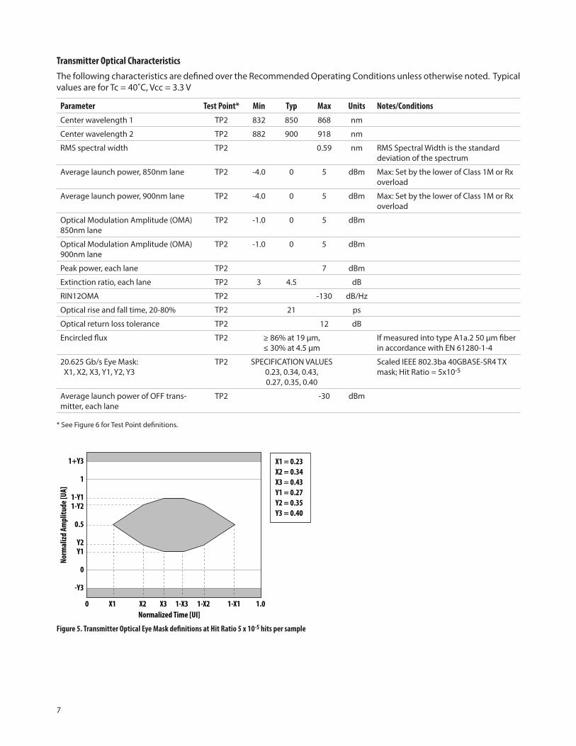
Transmitter Optical CharacteristicsThe following characteristics are defined over the Recommended Operating Conditions unless otherwise noted. Typical values are for Tc = 40˚C, Vcc = 3.3 V
Parameter Test Point* Min Typ Max Units Notes/ConditionsCenter wavelength 1 TP2 832 850 868 nm
Center wavelength 2 TP2 882 900 918 nm
RMS spectral width TP2 0.59 nm RMS Spectral Width is the standard deviation of the spectrum
Average launch power, 850nm lane TP2 -4.0 0 5 dBm Max: Set by the lower of Class 1M or Rx overload
Average launch power, 900nm lane TP2 -4.0 0 5 dBm Max: Set by the lower of Class 1M or Rx overload
Optical Modulation Amplitude (OMA) 850nm lane
TP2 -1.0 0 5 dBm
Optical Modulation Amplitude (OMA) 900nm lane
TP2 -1.0 0 5 dBm
Peak power, each lane TP2 7 dBm
Extinction ratio, each lane TP2 3 4.5 dB
RIN12OMA TP2 -130 dB/Hz
Optical rise and fall time, 20-80% TP2 21 ps
Optical return loss tolerance TP2 12 dB
Encircled flux TP2 ≥ 86% at 19 µm,≤ 30% at 4.5 µm
If measured into type A1a.2 50 µm fiber in accordance with EN 61280-1-4
20.625 Gb/s Eye Mask: X1, X2, X3, Y1, Y2, Y3
TP2 SPECIFICATION VALUES0.23, 0.34, 0.43,0.27, 0.35, 0.40
Scaled IEEE 802.3ba 40GBASE-SR4 TX mask; Hit Ratio = 5x10⁻⁵
Average launch power of OFF trans-mitter, each lane
TP2 -30 dBm
* See Figure 6 for Test Point definitions.
Figure 5. Transmitter Optical Eye Mask definitions at Hit Ratio 5 x 10⁻⁵ hits per sample
Norm
alizd
Am
plitu
de [U
A]
1-Y2
Y2
0.5
1-Y1
Y1
1+Y3
-Y3
Normalized Time [UI]0 X1 X2 1-X2 1-X1 1.0X3 1-X3
1
0
X1 = 0.23X2 = 0.34 X3 = 0.43 Y1 = 0.27 Y2 = 0.35 Y3 = 0.40

8
Receiver Optical CharacteristicsThe following characteristics are defined over the Recommended Operating Conditions unless otherwise noted. Typical values are for Tc = 40˚C, Vcc = 3.3 V
Parameter Test Point* Min Typ Max Units Notes/ConditionsCenter wavelength 1 TP3 850 nm
Center wavelength 2 TP3 900 nm
Damage Threshold [1] TP3 +7.0 dBm
Maximum Average power at receiver input, each lane (overload)
TP3 +5.0 dBm
Transceiver Reflectance TP3 -15 dB
Peak power, each lane TP3 7 dBm
Optical Modulation Amplitude (OMA), 850nm lane (unstressed sensitivity) TP3 -7.1 dBm BER = 1e-12
Optical Modulation Amplitude (OMA), 900nm lane (unstressed sensitivity) TP3 -7.7 dBm BER = 1e-12
Stressed receiver sensitivity in OMA, 850nm lane TP3 -4.5 -3.83 dBm BER = 1e-12
Stressed receiver sensitivity in OMA, 900nm lane TP3 -4.5 -3.86 dBm BER = 1e-12
Conditions of stressed receiver sensitivity: [2] TP3
Vertical Eye Closure Penalty, 850nm TP3 2.4 dB
Vertical Eye Closure Penalty, 900nm TP3 3.1 dB
Stressed eye Jitter, each lane TP3 0.13 UI
LOS Assert TP3 -30 -9.1 dBm
LOS De-Assert (850nm) TP3 -8.6 dBm
LOS De-Assert (900nm) TP3 -8.6 dBm
LOS Hysteresis TP3 0.5 dB
* See Figure 6 for Test Point definitions.Notes:1. The receiver shall be able to tolerate, without damage, continuous exposure to a modulated optical input signal having this power level on one
lane. The receiver does not have to operate correctly at this input power.2. Vertical eye closure penalty and stressed eye jitter are test conditions for measuring stressed receiver sensitivity. They are not characteristics of the
receiver.
TP0: Host ASIC transmitter output at ASIC package contact on the Host boardTP1: Host ASIC transmitter output across the Host Board at the input side of the Host QSFP+ electrical connectorTP2: QSFP+ transmitter LC Duplex optical output at the end of a 2m to 5m patch cordTP3: QSFP+ receiver LC Duplex optical input at the end of the fiberTP4a: QSFP+ receiver electrical output at the input side of the Host QSFP+ electrical connectorTP4: QSFP+ receiver electrical output at the output side of the Host QSFP+ electrical connectorTP5: Host ASIC receiver input at ASIC package contact on the Host board
Figure 6. Test point definitions
QSFP + RXQSFP + TX
Elec
trica
lCo
nnec
tor
Fiber
Optic
al P
atch
Cord
Elec
trica
lCo
nnec
tor
TP 5TP 4aTP 2TP 1a TP 4TP 0 TP 1 TP 3
ASIC/SerDes
ASIC/SerDes
9
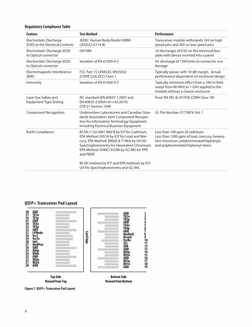
Regulatory Compliance Table
Feature Test Method PerformanceElectrostatic Discharge(ESD) to the Electrical Contacts
JEDEC Human Body Model (HBM)(JESD22-A114-B)
Transceiver module withstands 1kV on high speed pins and 2kV on low speed pins
Electrostatic Discharge (ESD) to Optical connector
GR1089 10 discharges of 8 kV on the electrical face-plate with device inserted into a panel
Electrostatic Discharge (ESD) to Optical connector
Variation of EN 61000-4-2 Air discharge of 15kV(min) to connector w/o damage
Electromagnetic Interference (EMI)
FCC Part 15 CENELEC EN55022(CISPR 22A) VCCI Class 1
Typically passes with 10 dB margin. Actual performance dependent on enclosure design
Immunity Variation of EN 61000-4-3 Typically minimum effect from a 10V/m field swept from 80 MHz to 1 GHz applied to the module without a chassis enclosure
Laser Eye Safety and Equipment Type Testing
IEC standard (EN 60825-1:2007 and EN 60825-2:2004+A1+A2:2010)CFR 21 Section 1040
Pout: EN AEL & US FDA CDRH Class 1M
Component Recognition Underwriters Laboratories and Canadian Stan-dards Association Joint Component Recogni-tion for Information Technology Equipment including Electrical Business Equipment
UL File Number: E173874, Vol. 1
RoHS Compliance BS EN 1122:2001 Mtd B by ICP for Cadmium, EPA Method 3051A by ICP for Lead and Mer-cury, EPA Method 3060A & 7196A by UV/Vis Spectrophotometry for Hexavalent Chromium. EPA Method 3540C/3550B by GC/MS for PPB and PBDE
BS EN method by ICP and EPA methods by ICP, UV/Vis Spectrophotometry and GC/MS.
Less than 100 ppm of cadmium,Less than 1000 ppm of lead, mercury, hexava-lent chromium, polybrominated biphenyls, and polybrominated biphenyl esters.
QSFP+ Transceiver Pad Layout
Figure 7. QSFP+ Transceiver Pad Layout
Card Edge
Top SideViewed from Top
TX3p
GNDTX1pTX1nGND
IntL
TX3n
GND
19
Bottom SideViewed from Bottom
VccRx
ModSelL
TX2pTX2nGND
TX4pTX4nGND
ResetL
ModPrsL
789101112131415161718
54321
6GND
RX1nRX1p
GND
RX3nRX3pGND
GNDRX2nGND
RX2p
RX4nRX4pGND
GND
SCLVccTx
SDA282726252423222120
313029
333435
32
36
3837
LPModeVcc1
10
Pins
Pin Logic Symbol Description Plug Sequence Notes1 GND Ground 1 12 CML-I Tx2n Transmitter Inverted Data Input 33 CML-I Tx2p Transmitter Non-Inverted Data Input 34 GND Ground 1 15 CML-I Tx4n Transmitter Inverted Data Input 36 CML-I Tx4p Transmitter Non-Inverted Data Input 37 GND Ground 1 18 LVTTL-I ModSelL Module Select 39 LVTTL-I ResetL Module Reset 310 Vcc Rx +3.3V Power supply receiver 2 211 LVCMOS-I/O SCL 2-wire serial interface clock 312 LVCMOS-I/O SDA 2-wire serial interface data 313 GND Ground 1 114 CML-O Rx3p Receiver Non-Inverted Data Output 315 CML-O Rx3n Receiver Inverted Data Output 316 GND Ground 1 117 CML-O Rx1p Receiver Non-Inverted Data Output 318 CML-O Rx1n Receiver Inverted Data Output 319 GND Ground 1 120 GND Ground 1 121 CML-O Rx2n Receiver Inverted Data Output 322 CML-O Rx2p Receiver Non-Inverted Data Output 323 GND Ground 1 124 CML-O Rx4n Receiver Inverted Data Output 325 CML-O Rx4p Receiver Non-Inverted Data Output 326 GND Ground 1 127 LVTTL-O ModPrsL Module Present 328 LVTTL-O IntL Interrupt 329 Vcc Tx +3.3V Power supply transmitter 2 230 Vcc1 +3.3V Power Supply 2 231 LVTTL-I LPMode Low Power Mode 332 GND Ground 1 133 CML-I Tx3p Transmitter Non-Inverted Data Input 334 CML-I Tx3n Transmitter Inverted Data Input 335 GND Ground 1 136 CML-I Tx1p Transmitter Non-Inverted Data Input 337 CML-I Tx1n Transmitter Inverted Data Input 338 GND Ground 1 1
Note 1. GND is the symbol for signal supply (power) common for the QSFP+ module. All are common within the QSFP+ module and all module voltages
are referenced to this potential unless otherwise noted. Connect these directly to the host board signal-common ground plane2. Vcc Rx, Vcc1 and Vcc Tx are the receiver and transmitter power supplies and shall be applied concurrently.

11
Figure 8. Case Temperature Measurement Point
Figure 9. Recommended Power Supply Filter
Figure 10. Transmitter Data Input Equivalent Circuit
QSFP+ Module
1 µH
0.1 µF
0.1 µF
1 µH
22 µF 0.1 µF 22 µF
Vcc_host = 3.3 Volt
Vcc Tx
Vcc Rx
GND
GND
0.1 µF
1 µH
22 µFVcc1
GND
22 µF
DPx
50 Ω
50 Ω
VCC33
Signal Path (Pos)
VCC25
DNx
VCC33
Signal Path (Neg)
VCC25
Measurement Point

12
Figure 11. Receiver Data Output Equivalent Circuit
Figure 12. TWS Interface Bus Timing
Doutp
Signal Path (Pos)Signal Path (Neg)
VCC25VCC25
Doutn
VCC33
50 Ω50 Ω
tSU,STO
SDA Out
SCL
START
tHD,SDA
tLOW
ReSTART STOP
tHIGH
tHD,DAT
tF tR
SDA In
tR
tAA tDH
tSU,DATtSU,SDA tFtBUFtBUF

13
Package Outline, Host PCB Footprint and Bezel Design
All dimensions in mmFigure 13. Mechanical Package Outline
TransmitterCenter Wavelength
850nm 900nm 53.00
48.80 29.60
1.00 2.25
8.50
18.35
12.90 6.02
72.40
122.27
18.35 18.00
14
All dimensions in mmFigure 14. QSFP+ Host Board Mechanical Footprint
Notes:1. Datum X & Y are established by the customer’s ducial2. Datum A is the top surface of the host board3. Location of the edge of PCB is application specic4. Finished hole size
Cross-hatched area denotescomponent and trace keep-out(except chassis ground)
This area denotescomponent keep-out(traces allowed)
22.15
19.00
3.107.60
1.1019
20
1
38
7.20
3.40
16.80
CK
17.90 REF.
Y
X
BASIC
BASIC
3.10
7.60
L
11.30 MIN.
10.60
37.00 MAX.
Ø1.05 ±0.0512 PLC
MØ0.10 A SK SL
9.006 PLC
15
191
2038
16.80
2.51
Ø1.55 ±0.05Ø0.05 A X SK
Ø1.55 ±0.05Ø0.05 A X Y
1
5.18
1
3
3
1.80 ±0.030.05 A C L-K
0.35 ±0.030.05 A CL-K
19.20 MAX.
2
15.02 MAX.
Datum Axis C
22.15
Notes:1. Centerline of Pad2. Surface traces permitted within this length3. Indicated holes are optional
0.80
0.20
0.20
7.40
7.00
C
K
L
All dimensions in mmFigure 15. QSFP+ Host Board Mechanical Footprint Detail
All dimensions in mmFigure 16. Host Board Bezel Design
10.15 ±0.1TYP A
0.15 ±0.1(Bottom of cut-out
in bezel to top ofPC Board)
20 ±0.1 TYP
R0.3 TYP
B
Bezel
21 ±0.11
43 ±0.32
37 MAX2
Notes:
Minimum pitch dimension for individual cages.
Dimension baseline is datum or .
3. Not recommended for PCI applications.2
1
K L

16
Control InterfaceThe control interface combines dedicated signal lines for ModSelL, LP Mode, ResetL, ModPrsL, IntL with two-wire serial (TWS), interface clock (SCL) and data (SDA), signals to provide users rich functionality over an efficient and easily used interface. The TWS interface is implemented as a slave device and compatible with industry standard two-wire serial protocol. It is scaled for 3.3 volt LVTTL. Outputs are high-z in the high state to support busing of these signals. Signal and timing characteristics are further defined in the Control I/O Characteristics section.
ModSelLThe ModSelL is an input signal. When held low by the host, the module responds to 2-wire serial communica-tion commands. The ModSelL allows the use of multiple QSFP+ modules on a single 2-wire interface bus. When the ModSelL is “High”, the module will not respond to or acknowledge any 2-wire interface communication from the host. ModSelL signal input node is biased to the “High” state in the module. In order to avoid conflicts, the host system shall not attempt 2-wire interface communica-tions within the ModSelL de-assert time after any QSFP+ modules are deselected. Similarly, the host must wait at least for the period of the ModSelL assert time before communicating with the newly selected module. The as-sertion and de-asserting periods of different modules may overlap as long as the above timing requirements are met.
ResetLThe ResetL signal is pulled to Vcc in the QSFP+ module. A low level on the ResetL signal for longer than the minimum pulse length (t_Reset_init) initiates a complete module reset, returning all user module settings to their default state. Module Reset Assert Time (t_init) starts on the rising edge after the low level on the ResetL pin is released. Dur-ing the execution of a reset (t_init) the host shall disregard all status bits until the module indicates a completion of the reset interrupt. The module indicates this by posting an IntL signal with the Data_Not_Ready bit negated. Note that on power up (including hot insertion) the module will post this completion of reset interrupt without requiring a reset.
LPModeLow power mode. When held high by host, the module is held at low power mode with power consumption meet-ing class 1 power level (1.5W). Under low power mode, high speed operation is not functional and all high speed indicators are not reliable while the TWS management in-terface is functional. When held low by host, the module operates in the normal mode.
ModPrsLModPrsL is pulled up to Vcc_Host on the host board and grounded in the module. The ModPrsL is asserted “Low” when inserted and de-asserted “High” when the module is physically absent from the host connector.
IntLIntL is an output signal. When “Low”, it indicates a possible module operational fault or a status critical to the host sys-tem. The host identifies the source of the interrupt using the 2-wire serial interface. The IntL signal is an open collec-tor output and must be pulled to host supply voltage on the host board. A corresponding soft status IntL signal is also available in the transceiver memory page 0 address 2 bit 1.
Soft Status and ControlA number of soft status signals and controls are available in the AFBR-79EBPZ transceiver memory and accessible through the TWS interface. Soft status signals include receiv-er LOS, transmitter LOS, and a transmitter fault. Some soft controls include transmitter disable (Tx_Dis), receiver output disable (Rx_Dis), transmitter squelch disable (Tx_SqDis), re-ceiver squelch disable (Rx_SqDis) and masking of status sig-nal in triggering IntL. All soft control entries are volatile.
Receiver LOSThe Receiver LOS status signal is on page 0 address 3 bits 0-3. Reeiver LOS is based on received optical power modula-tion amplitude (OMA). The status register is latched and it is cleared on read. The first 20G lane RX is mapped to the first 2 RX lanes as defined in QSFP, and the second 20G RX lane is mapped to the third and fourth RX lanes as defined in QSFP MSA.
Transmitter LOSThe transmitter LOS status signal is on page 0 address 3 bits 4-7. Transmitter LOS is based on input differential voltage. The status register is latched and it is cleared on read.
Transmitter FaultTransmitter fault status is reported in page0 register 4. Trans-mitter fault will be asserted when the laser cannot be con-trolled anymore, or it could cause harm to eyes as defined by the eyesafety regulation. The status is latched and cleared on read.
Transmitter DisableThe transmitter Disable control is on page 0 address register 86. Because 2 10G input lanes are muxed into one 20G TX optical lane, either one of these lanes getting disabled will disable the 20G optical signal.
Receiver DisableThe received disable control is on page 3 address 241 bits 4-7. Asserting any bit would cause the corresponding lane’s RX output to be disabled.
Transmitter Squelch DisableThe Transmitter squelch disable control is on page 3 address 240 bits 0-3. AFBR-79EBPZ transceivers have transmitter squelch enabled as default.
Receiver Squelch DisableThe receiver squelch disable control is on page 3 address 240 bits 4-7. AFBR-79EBPZ transceivers have receiver output squelch enabled as default.
17
I/O Timing for Control and Status FunctionsThe following characteristics are defined over the Recommended Operating Conditions unless otherwise noted.
Parameter Symbol Min Max Units ReferenceInitialization Time t_init 2000 ms Time from power on, hot plug or rising edge of Reset until the
module is fully functional. This time does not apply to non Power level 0 modules in the Low Power state
LPMode Assert Time
ton_LPMode 100 µs Time from assertion of LPMode until the module power con-sumption enters power level 1
Interrupt Assert Time
ton_IntL 200 ms Time from occurrence of condition triggering IntL until Vout:IntL=Vol
Interrupt De-assert Time
toff_IntL 500 µs Time from clear on read operation of associated flag until Vout:IntL=Voh. This includes deassert times for RX LOS, TX Fault and other flag bits
Reset Init Assert Time
t_reset_init 2 µs A Reset is generated by a low level longer than the minimum reset pulse time present on the ResetL pin
Reset Assert Time t_reset 2000 ms Time from rising edge on the ResetL pin until the module is fully functional
Serial Bus Hardware Ready Time
t_serial 2000 ms Time from power on until module responds to data transmission over the 2-wire serial bus
Monitor Data Ready Time
t_data 2000 ms Time from power on to data not ready, bit 0 of Byte 2, deasserted and IntL asserted
RX LOS Assert Time ton_los 100 ms Time from RX LOS state to RX LOS bit set and IntL asserted
TX Fault Assert Time
ton_Txfault 200 ms Time from TX Fault state to TX fault bit set and IntL asserted
Flag Assert Time ton_Flag 200 ms Time from occurrence of condition triggering flag to associated flag bit set and IntL asserted.
Mask Assert Time ton_Mask 100 ms Time from mask bit set until associated IntL assertion is inhibited
Mask Deassert Time toff_Mask 100 ms Time from mask bit cleared until associated IntL operation resumes
Power Set Assert Time
ton_Pdown 100 ms Time from P_Down bit set until module power consumption enters power level 1
Power Set Deassert Time
toff_Pdown 300 ms Time from P_Down bit cleared until the module is fully func-tional
RX Squelch Assert Time
ton_Rxsq 80 µs Time from loss of RX input signal until the squelched output condition is reached
RX Squelch Deas-sert Time
toff_Rxsq 1 ms Time from resumption of RX input signals until normal RX output condition is reached
TX Squelch Assert Time
ton_Txsq 400 ms Time from loss of TX input signal until the squelched output condition is reached
TX Squelch Deas-sert Time
toff_Txsq 400 ms Time from resumption of TX input signals until nominal TX out-put condition is reached
TX Disable Assert Time
ton_txdis 100 ms Time from TX Disable bit set until optical output falls below 10% of nominal
TX Disable Deassert Time
toff_txdis 400 ms Time from TX Disable bit cleared until optical output rises above 90% of nominal
RX Output Disable Assert Time
ton_rxdis 100 ms Time from RX Output Disable bit set until RX output falls below 10% of nominal
RX Output Disable Deassert Time
toff_rxdis 100 ms Time from RX Output Disable bit cleared until RX output rises above 90% of nominal
Squelch Disable Assert Time
ton_sqdis 100 ms This applies to RX and TX Squelch and is the time from bit set until squelch functionality is disabled
Squelch Disable Deassert Time
toff_sqdis 100 ms This applies to RX and TX Squelch and is the time from bit cleared until squelch functionality is enabled
18
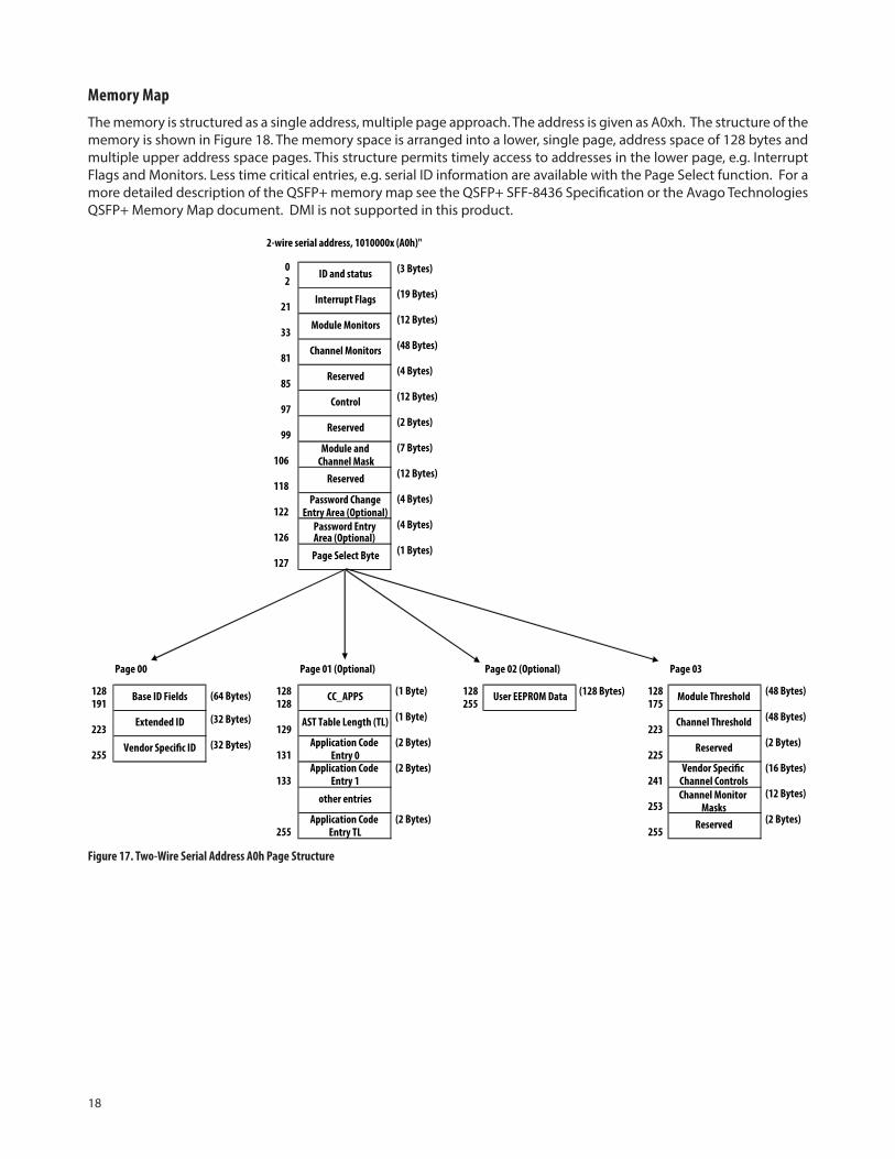
Memory MapThe memory is structured as a single address, multiple page approach. The address is given as A0xh. The structure of the memory is shown in Figure 18. The memory space is arranged into a lower, single page, address space of 128 bytes and multiple upper address space pages. This structure permits timely access to addresses in the lower page, e.g. Interrupt Flags and Monitors. Less time critical entries, e.g. serial ID information are available with the Page Select function. For a more detailed description of the QSFP+ memory map see the QSFP+ SFF-8436 Specification or the Avago Technologies QSFP+ Memory Map document. DMI is not supported in this product.
Figure 17. Two-Wire Serial Address A0h Page Structure
2-wire serial address, 1010000x (A0h)"
02
(19 Bytes)21
(12 Bytes)33
(48 Bytes)81
(4 Bytes)85
(12 Bytes)97
(2 Bytes)99
(7 Bytes)106
(12 Bytes)118
(4 Bytes)122
(4 Bytes)126
(1 Bytes)127
Page 03Page 02 (Optional)Page 01 (Optional) Page 00
128 (128 Bytes)128128128175255128191
(32 Bytes)
(64 Bytes)
(1 Byte)
(1 Byte)
(48 Bytes)
(48 Bytes)
129223 223(32 Bytes) (2 Bytes) (2 Bytes)
131255 225(2 Bytes) (16 Bytes)
133 241(12 Bytes)
253(2 Bytes) (2 Bytes)
255 255Application Code
Entry TLReserved
Application Code Entry 1
Vendor SpecicChannel Controls
other entries Channel Monitor Masks
AST Table Length (TL)Extended ID Channel Threshold
Application Code Entry 0
Vendor Specic ID Reserved
Module ThresholdUser EEPROM DataCC_APPSBase ID Fields
Reserved
Password Change Entry Area (Optional)
Password Entry Area (Optional) Page Select Byte
Reserved
Control
Reserved
Module and Channel Mask
ID and status
Interrupt Flags
Module Monitors
Channel Monitors
(3 Bytes)

For product information and a complete list of distributors, please go to our web site: www.avagotech.com
Avago, Avago Technologies, and the A logo are trademarks of Avago Technologies in the United States and other countries.Data subject to change. Copyright © 2005-2015 Avago Technologies. All rights reserved. AV02-4528EN - August 11, 2015
Lane OrderingCare must be taken to reassemble XLPPI information at the host receiver due to uncertainty of phase alignment of Lane A and B between transmit and receive multiplexer stages. The transceiver will not assure XLPPI lane assignment end-to-end in order to keep complexity and power dissipation in the QSFP+ footprint to a minimum. Once end-to-end com-munication has been established and lane ordering established, lane assignment may change again each time the link is re-established, such as when TX LOS, RX LOS, or when module power cycling occurs.
Figure 18. Transceiver Lane Ordering Limitations
2:1 ElectricalMultiplexer
2:1 ElectricalMultiplexer
XLPPI Lane A
XLPPI Lane B
XLPPI Lane C
XLPPI Lane D
2:1 ElectricalMultiplexer
2:1 ElectricalMultiplexer
1 x 20Gb Optical Lane
1 x 20Gb Optical Lane
XLPPI Lane A or B
XLPPI Lane A or B
XLPPI Lane C or D
XLPPI Lane C or D