Embed Size (px)
Citation preview
Curriculum & Syllabus
of
M.E. VLSI Design
(For the batch admitted in 2010-11 onwards)
K.S.RANGASAMY COLLEGE OF TECHNOLOGYTIRUCHENGODE – 637 215
(An Autonomous Institution affiliated to Anna University Chennai and approved by AICTE New Delhi)

2
BoS Chairman Prepared By PVL: M.E. VLSI DESIGN - REGULATION 2010 - SYLLABUS
K.S.Rangasamy College of Technology -Autonomous Regulation R 2010
Department Electronics and CommunicationEngineering
Programme Code & Name PVL : M.E. VLSI Design

3
BoS Chairman Prepared By PVL: M.E. VLSI DESIGN - REGULATION 2010 - SYLLABUS
K.S.Rangasamy College of Technology , Tiruchengode - 637215Curriculum for the Programmes under Autonomous Scheme
Regulation R 2010Department Department of Electronics and Communication EngineeringProgramme Code & Name PVL : M.E (VLSI Design)
Semester ICourseCode Course Name
Hours/ Week Credit Maximum marksL T P C CA ES Total
THEORY
10 PVL 101 Applied Mathematics(PAE,PVL) 3 1 0 4 50 50 100
10 PVL 102 VLSI Design Techniques(PAE,PVL) 3 0 0 3 50 50 100
10 PVL 103 Advanced Digital System Design(PAE,PVL) 3 1 0 4 50 50 100
10 PVL 104 Embedded Systems(PAE,PVL) 3 0 0 3 50 50 100
10 PVL 105 Device Modeling 3 0 0 3 50 50 10010 PVL E1* Elective I 3 0 0 3 50 50 100
PRACTICAL10 PVL 106 VLSI Simulation Laboratory 0 0 3 2 50 50 10010 PVL 107 Embedded Systems Laboratory 0 0 3 2 50 50 100
Total 18 2 6 24 800Semester II
CourseCode Course Name
Hours/ Week Credit Maximum marksL T P C CA ES Total
THEORY
10 PVL 201 CAD of VLSI Circuits(PAE,PVL) 3 0 0 3 50 50 100
10 PVL 202 Analog VLSI circuits(PAE,PVL) 3 0 0 3 50 50 100
10 PVL 203Advanced Computer Architecture andParallel Processing(PAE,PVL)
3 0 0 3 50 50 100
10 PVL 204 ASIC Design 3 0 0 3 50 50 10010 PVL E2* Elective II 3 0 0 3 50 50 10010 PVL E3* Elective III 3 0 0 3 50 50 100
PRACTICAL
10 PVL 205 VLSI Design and ImplementationLaboratory 0 0 3 2 50 50 100
10 PVL 206 Technical Report Preparation andPresentation 0 0 2 0 100 00 100
Total 18 0 5 20 800

4
BoS Chairman Prepared By PVL: M.E. VLSI DESIGN - REGULATION 2010 - SYLLABUS
K.S.Rangasamy College of Technology , Tiruchengode - 637215Curriculum for the Programmes under Autonomous Scheme
Regulation R 2010Department Department of Electronics and Communication EngineeringProgramme Code & Name PVL : M.E VLSI DESIGN
Semester IIICourse
Code Course NameHours/ Week Credit Maximum marks
L T P C CA ES TotalTHEORY
10 PVL 301Arm Architecture andProgramming(PAE,PVL)
3 0 0 3 50 50 100
10 PVL E4* Elective IV 3 0 0 3 50 50 10010 PVL E5* Elective V 3 0 0 3 50 50 100
PRACTICAL10 PVL 302 Project Work - Phase I 0 0 12 2 100 00 100
Total 9 0 12 11 400Semester IV
CourseCode Course Name
Hours/ Week Credit Maximum marksL T P C CA ES Total
PRACTICAL10 PVL 401 Project Work - Phase II 0 0 40 10 50 50 100
Total 0 0 40 10 100

5
BoS Chairman Prepared By PVL: M.E. VLSI DESIGN - REGULATION 2010 - SYLLABUS
K.S.Rangasamy College of Technology , Tiruchengode - 637215Curriculum for the Programmes under Autonomous Scheme
Regulation R 2010Department Department of Electronics and Communication EngineeringProgramme Code &Name PVL : M.E. VLSI Design
Course Code Course NameHours/ Week Credit Maximum marks
L T P C CA ES TotalElectives
10 PVL E01 Nano Electronics 3 0 0 3 50 50 10010 PVL E02 Neural Networks and its Applications 3 0 0 3 50 50 100
10 PVL E03 Semiconductor Memory Design andTesting 3 0 0 3 50 50 100
10 PVL E04 Low Power VLSI Design 3 0 0 3 50 50 10010 PVL E05 Computational Intelligent Techniques 3 0 0 3 50 50 100
10 PVL E06 DSP Processor Architecture andProgramming 3 0 0 3 50 50 100
10 PVL E07 VLSI Signal Processing 3 0 0 3 50 50 10010 PVL E08 MEMS System Design 3 0 0 3 50 50 10010 PVL E09 System On Chip 3 0 0 3 50 50 10010 PVL E10 Physical Design of VLSI Circuits 3 0 0 3 50 50 10010 PVL E11 Digital Image Processing 3 0 0 3 50 50 10010 PVL E12 VLSI Technology 3 0 0 3 50 50 10010 PVL E13 Linear Algebra 3 0 0 3 50 50 10010 PVL E14 CMOS VLSI Design 3 0 0 3 50 50 10010 PVL E15 VLSI for Wireless Communication 3 0 0 3 50 50 10010 PVL E16 FPGA-based System Design 3 0 0 3 50 50 100
6
BoS Chairman Prepared By PVL: M.E. VLSI DESIGN - REGULATION 2010 - SYLLABUS
K.S.Rangasamy College of Technology - Autonomous Regulation R 2010
Department Electronics and CommunicationEngineering Programme Code & Name PVL : M.E. VLSI Design
Semester I
Course Code Course NameHours/ Week Credit Maximum Marks
L T P C CA ES Total
10 PVL 101 APPLIED MATHEMATICS(PAE,PVL) 3 1 0 4 50 50 100
Objective(s)To develop efficient algorithms for solving numerical methods, to acquire skills in handlingsituation involving random variable. To learn the basics and gained the skill for specializedstudies and research.
1 LINEAR ALGEBRAIC EQUATION AND EIGEN VALUEPROBLEMS Total Hrs 12
System of equations- Solution by Gauss Elimination, Gauss-Jordan and LU decomposition method- Jacobi,Gauss-Seidal iteration method- Eigen values of a matrix by Jacobi and Power method.
2 WAVE EQUATION Total Hrs 12Solution of initial and boundary value problems- Characteristics- D’Alembert’s Solution - Significance ofcharacteristic curves - Laplace transform solutions for displacement in a long string - a long string under itsweight - a bar with prescribed force on one end- free vibrations of a string.
3 SPECIAL FUNCTIONS Total Hrs 12Bessel’s equation - Bessel Functions- Legendre’s equation - Legendre polynomials - Rodrigue’s formula -Recurrence relations- generating functions and orthogonal property for Bessel functions - Legendrepolynomials.
4 RANDOM VARIABLES Total Hrs 12One dimensional Random Variable - Moments and MGF – Binomial, Poisson, Geometrical, NormalDistributions- Two dimensional Random Variables – Marginal and Conditional Distributions – Covariance andCorrelation Coefficient - Functions of Two dimensional random variable.
5 QUEUEING THEORY Total Hrs 12Single and Multiple server Markovian queueing models - Steady state system size probabilities – Little’sformula - priority Queues - M/G/1 queueing system – P.K. formula.Total hours to be taught 60Reference(s) :
1 Sankara Rao.K. “Introduction to Partial Differential Equation “, PHI, 1995.2 Taha. H.A., “Operations Research - An Introduction “ 6th Edition, PHI, 1997.
3 Jain M.K. Iyengar, S.R.K. & Jain R.K., “International Methods for Scientific and EngineeringComputation”, New Age International (P) Ltd, Publlishers 2003.

7
BoS Chairman Prepared By PVL: M.E. VLSI DESIGN - REGULATION 2010 - SYLLABUS
K.S.Rangasamy College of Technology - Autonomous Regulation R 2010
Department Electronics and CommunicationEngineering Programme Code & Name PVL : M.E. VLSI Design
Semester I
Course Code Course NameHours/ Week Credit Maximum Marks
L T P C CA ES Total
10 PVL 102 VLSI DESIGN TECHNIQUES(PAE,PVL) 3 0 0 3 50 50 100
Objective(s) To learn the CMOS processing technology and basic CMOS circuits, CMOS transistortheory and logic design. To study about verilog HDL Programme
1 INTRODUCTION TO MOS TRANSISTOR THEORY Total Hrs 9MOS transistors, CMOS logic, MOS transistor theory – Introduction, Enhancement mode transistor action, IdealI-V characteristics, Simple MOS capacitance Models, Detailed MOS gate capacitance model, Detailed MOSDiffusion capacitance model, Non ideal I-V effects, DC transfer characteristics, VLSI Design flow.
2 CMOS TECHNOLOGY AND DESIGN RULE Total Hrs 9CMOS fabrication and Layout, CMOS technologies, P-Well process, N-Well process, twin-tub process, MOSlayers stick diagrams and Layout diagram, Layout design rules, Latch up in CMOS circuits, CMOS processenhancements, Technology – related CAD issues, Fabrication and packaging.
3 CIRCUIT CHARACTERISATION & PERFORMANCEESTIMATION Total Hrs 9
Determination of Pull-up to Pull-down ratio for NMOS inverter, super buffers, Driving large capacitance loads,Circuits families, transmission gates, Delay estimation, Power dissipation, Design margin, Scaling of MOSCircuits.
4 VLSI SYSTEM COMPONENTS CIRCUITS Total Hrs 9Multiplexers, Decoders, comparators, priority encoders, Shift registers. Arithmetic circuits – Ripple carryadders, Carry look ahead adders, High-speed adders, Multipliers
5 VERILOG HARDWARE DESCRIPTION LANGUAGE Total Hrs 9Overview of digital design with Verilog HDL, hierarchical modeling concepts, basic concepts, modules and portdefinitions, gate level modeling, data flow modeling, behavioral modeling, task & functions, Test Bench.Total hours to be taught 45Reference(s) :
1 Neil H.E.Weste, David Harris and Ayan Banerjee, “CMOS VLSI Design a circuits and systemsperspective, Third Edition, Pearson Education, 2010.
2 Douglas A.Pucknell and Kamran Eshraghian, “Basic VLSI Design”, Third Edition, Prentice-Hall ofIndia2004.
3 Samir Palnitkar, “Verilog HDL a Guide to Digital Design and Synthesis”, Second Edition, PearsonEducation, 2010.
4 John P.Uyemura “Introduction to VLSI Circuits and Systems”, Wiley India Edition, 2006.
5 Neil H.E. Weste and Kamran Eshraghian, Principles of CMOS VLSI Design, Pearson EducationASIA, 2nd edition, 2000.

8
BoS Chairman Prepared By PVL: M.E. VLSI DESIGN - REGULATION 2010 - SYLLABUS
K.S.Rangasamy College of Technology - Autonomous Regulation R 2010
Department Electronics and CommunicationEngineering Programme Code & Name PVL : M.E. VLSI Design
Semester I
Course Code Course NameHours/ Week Credi
t Maximum Marks
L T P C CA ES Total
10 PVL 103 ADVANCED DIGITAL SYSTEMDESIGN(PAE,PVL) 3 1 0 4 50 50 100
Objective(s) To learn how to design programmable logic circuits, logic synthesis compiler based on VHDLand to determine the types of fault that occur in digital circuits.
1 SEQUENTIAL CIRCUIT DESIGN Total Hrs 12Analysis of Clocked Synchronous Sequential Networks (CSSN) Modeling of CSSN –State Stable Assignmentand Reduction – Design of CSSN – Design of Iterative Circuits – ASM Chart – ASM Realization.
2 ASYNCHRONOUS SEQUENTIAL CIRCUIT DESIGN Total Hrs 12Analysis of Asynchronous Sequential Circuit (ASC) – Flow Table Reduction – Races in ASC – State Assignment– Problem and the Transition Table – Design of ASC – Static and Dynamic Hazards – Essential Hazards – DataSynchronizers – Designing Vending Machine Controller – Mixed Operating Mode Asynchronous Circuits.
3 FAULT DIAGNOSIS AND TESTABILITY ALGORITHMS Total Hrs 12Fault Table Method – Path Sensitization Method – Boolean Difference Method – Kohavi Algorithm – ToleranceTechniques – The Compact Algorithm – Practical PLA’s – Fault in PLA – Test Generation – Masking Cycle –DFT Schemes – Built-in Self Test.
4 SYNCHRONOUS DESIGN USING PROGRAMMABLEDEVICES Total Hrs 12
EPROM to Realize a Sequential Circuit – Programmable Logic Devices – Designing a Synchronous SequentialCircuit using a GAL – EPROM – Realization State machine using PLD – FPGA – Xilinx FPGA – Xilinx 2000 -Xilinx 3000.
5 SYSTEM DESIGN USING VHDL Total Hrs 12VHDL Description of Combinational Circuits – Arrays – VHDL Operators –Compilation and Simulation of VHDLCode – Modelling using VHDL – Flip Flops – Registers – Counters – Sequential Machine – Combinational LogicCircuits – VHDL Code for – Serial Adder, Binary Multiplier – Binary Divider – complete Sequential Systems –Design of a Simple Microprocessor.Total hours to be taught 60Reference(s) :
1 Donald G. Givone “Digital principles and Design” Tata McGraw Hill 2002.2 John M Yarbrough “Digital Logic appns. and Design” Thomson Learning, 2001.3 Nripendra N Biswas “Logic Design Theory” Prentice Hall of India, 2001.4 Charles H. Roth Jr. “Digital System Design using VHDL” Thomson Learning, 1998.

9
BoS Chairman Prepared By PVL: M.E. VLSI DESIGN - REGULATION 2010 - SYLLABUS
K.S.Rangasamy College of Technology - Autonomous Regulation R 2010
Department Electronics and CommunicationEngineering Programme Code & Name PVL : M.E. VLSI Design
Semester I
Course Code Course NameHours/ Week Credit Maximum Marks
L T P C CA ES Total
10 PVL 104 EMBEDDED SYSTEMS(PAE,PVL) 3 0 0 3 50 50 100
Objective(s) To understand the concept of embedded Architecture and emphasis the knowledge ofvarious processors and embedded networking.
1 EMBEDDED SYSTEMS Total Hrs 9Embedded Computers, Characteristics of Embedded Computing Applications, Challenges in EmbeddedComputing system design, Embedded system design process- Requirements, Specification, ArchitecturalDesign, Designing Hardware and Software Components, System Integration, Formalism for System Design-Structural Description, Behavioral Description, Design Example: Model Train Controller.
2 MICROCHIP PIC MICROCONTROLLER -16F87X Total Hrs 9PIC Microcontrollers 16F87X -PIC development tools-CPU Architecture and pipelining-program memoryconsiderations-register file structure and addressing modes-CPU Registers-Instruction set-Loop Timesubroutine-Interrupts-Timers-Capture mode-compare mode and PWM mode.
3 PIC MICROCONTROLLER PERIPHERAL FEATURES Total Hrs 9I/O Port Expansion-Synchronous serial Port (SSP)-Serial Peripheral Interface (SPI)-, I2C Bus for peripheral chipaccess- Analog to Digital converter- UART – Baud Rate – Data Handling – Initialization, special features- SerialProgramming – Parallel Slave Port.
4 EMBEDDED SYSTEM CO-DESIGN Total Hrs 9Distributed Embedded Architecture- Hardware and Software Architectures, Networks for embedded systems-I2C, CAN Bus, SHARC link ports, Ethernet, Myrinet, Internet, Network-Based design- CommunicationAnalysis, system performance Analysis, Hardware platform design, Allocation and scheduling, DesignExample: Elevator Controller
5 REAL-TIME OPERATING SYSTEMS Total Hrs 9Semaphores and Shared Data Operating System services – Memory Management, Interrupt Routines in anRTOS environment, Basic design using RTOS. Services –I/O subsystems – Network operating systems –Interrupt Routines in RTOS Environment – RTOS Task scheduling models, Interrupt – IEEEstandard POSIX functions for standardization of RTOS and inter-task communication functions.
Total hours to be taught 45Reference(s) :
1 John B Pitman, “Design with PIC Micro controllers”, Pearson Education Asia, fourteenth reprint 2004
2 Wayne Wolf, Computers as Components: Principles of Embedded Computing System Design, MorganKaufman Publishers, 2001.
3 Raj kamal ”Embedded System Architecture, Programming and Design”, Second edition ,Tata McGraw-Hill, 2008.
4 David E. Simon, “An Embedded Software Primer”, Pearson Education Asia, 2001.5 C. M. Krishna and K. G. Shin , Real-Time Systems, ,McGraw-Hill, 1997
6 Frank Vahid and Tony Givargi Embedded System Design: A Unified Hardware/Software Introduction, s,John Wiley & Sons, 2000.

10
BoS Chairman Prepared By PVL: M.E. VLSI DESIGN - REGULATION 2010 - SYLLABUS
K.S.Rangasamy College of Technology - Autonomous Regulation R 2010
Department Electronics and CommunicationEngineering Programme Code & Name PVL : M.E. VLSI Design
Semester I
Course Code Course NameHours/ Week Credit Maximum Marks
L T P C CA ES Total10 PVL 105 DEVICE MODELING 3 0 0 3 50 50 100
Objective(s) To study the semiconductor physics of devices, various modeling techniques for diodes, BJTsand MOSFET and various fabrication techniques.
1 INTRODUCTION TO SEMICONDUCTOR PHYSICS,INTEGRATED PASSIVE DEVICES Total Hrs 9
Review of Quantum Mechanics, Boltzman transport equation. Continuity equation, Poisson equation, Typesand Structures of resistors and capacitors in monolithic technology - dependence of model parameters onstructure.
2 INTEGRATED DIODES Total Hrs 9Junction and Schottky diodes in monolithic technologies - static and dynamic behavior - small and large signalmodels - SPICE models.
3 INTEGRATED BIPOLAR TRANSISTOR Total Hrs 9Types and structures in monolithic technologies - Basic model (Eber - Moll) - Gunmel - poon model - dynamicmodel, parasitic effects - SPICE model - parameter extraction.
4 INTEGRATED MOS TRANSISTOR Total Hrs 9nMOS and pMOS Transistor - Threshold voltage - Threshold voltage equations - MOS device equations -
Basic DC equations Second order effects - MOS models - Small signal AC Characteristics - MOSFET SPICEmodel level 1,2,3 and 4.
5 VLSI FABRICATION TECHNIQUES, EMI ENVIRONMENT Total Hrs 9An overview of wafer fabrication, wafer processing- oxidation - patterning - Diffusion - Ion implantation -Deposition - Silicon Gate nmos process - CMOS process - nwell - pwell -Twin tub - Silicon on Insulator - CMOSprocess enhancements - Interconnects circuit elements, Sources of EMI and EMC, Definitions and units ofparameters, Radiation hazards to human beings.Total hours to be taught 45Reference(s) :
1 Giuseppe Massobrio and Paolo Antogentti, “Semiconductor Device Modeling with SPICE” 2nd Edition,McGraw-Hill Inc, New York, 1993
2 Neil H.E.Weste and Kamran Eshraghian, Principles of CMOS VLSI Design, 2nd Edition, PearsonEducation Asia, 2000.
3 Sze S.M.,”Physics of Semiconductor Devices” 2nd Edition McGraw Hill, New York, 19814 Ben. G. Streetman, "Solid State Circuits", Prentice hall, 19975 Tyagi M.S. "Introduction to Semi-Conductor Materials and Devices", John Wiley ,20036 Tor.A.Fijedly, “Introduction to Device Modeling and Circuit Simulation”, Wiley-interscience, 19977 Daniel Forty, “MOSFET Modeling with SPICE”, Prentice Hall, 19978 Roulston E.J., “Bipolar Semiconductor Devices”, Mc-Graw Hill, 19909 Nicollian E.H.and J.R.Brews, “MOS Physics and Technology,” John Wiley, 1982.
11
BoS Chairman Prepared By PVL: M.E. VLSI DESIGN - REGULATION 2010 - SYLLABUS
K.S.Rangasamy College of Technology - Autonomous Regulation R 2010
Department Electronics and CommunicationEngineering Programme Code & Name PVL : M.E. VLSI Design
Semester I
Course Code Course NameHours/ Week Credit Maximum Marks
L T P C CA ES Total
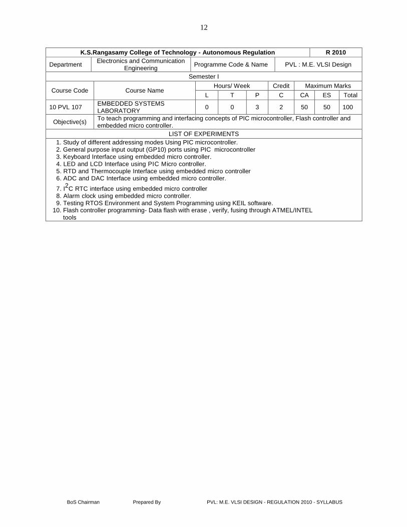
10 PVL 106 VLSI SIMULATIONLABORATORY 0 0 3 2 50 50 100
Objective(s) To teach the programming concepts using Verilog HDL, VHDL and usage of Xillinx ISE Tool.LIST OF EXPERIMENTS
1. Design and Simulation of Arithematic /logic operator circuits using verilog/VHDL2. Modeling of Combinational/Sequential Circuits Using Verilog HDL3. Simulation of schematic /RTL using Xilinx ISE Tool4. ARBITER Design using state diagram in Xilinx ISE Tool5. Simulation of HDL Netlist using Test bench6. Modeling of MAC unit using verilog / VHDL7. Modeling of ALU using verilog / VHDL8. Design and 8-bit signed multiplication algorithm using verilog / VHDL9. Design and technological mapping of RTL netlist in Xilinx ISE tool
10. Place & route and back annotation for FPGA
12
BoS Chairman Prepared By PVL: M.E. VLSI DESIGN - REGULATION 2010 - SYLLABUS
K.S.Rangasamy College of Technology - Autonomous Regulation R 2010
Department Electronics and CommunicationEngineering Programme Code & Name PVL : M.E. VLSI Design
Semester I
Course Code Course NameHours/ Week Credit Maximum Marks
L T P C CA ES Total
10 PVL 107 EMBEDDED SYSTEMSLABORATORY 0 0 3 2 50 50 100
Objective(s) To teach programming and interfacing concepts of PIC microcontroller, Flash controller andembedded micro controller.
LIST OF EXPERIMENTS1. Study of different addressing modes Using PIC microcontroller.2. General purpose input output (GP10) ports using PIC microcontroller3. Keyboard Interface using embedded micro controller.4. LED and LCD Interface using PIC Micro controller.5. RTD and Thermocouple Interface using embedded micro controller6. ADC and DAC Interface using embedded micro controller.7. I2C RTC interface using embedded micro controller8. Alarm clock using embedded micro controller.9. Testing RTOS Environment and System Programming using KEIL software.
10. Flash controller programming- Data flash with erase , verify, fusing through ATMEL/INTELtools
13
BoS Chairman Prepared By PVL: M.E. VLSI DESIGN - REGULATION 2010 - SYLLABUS
K.S.Rangasamy College of Technology - Autonomous Regulation R 2010
Department Electronics and CommunicationEngineering Programme Code & Name PVL : M.E. VLSI Design
Semester II
Course Code Course NameHours/ Week Credit Maximum Marks
L T P C CA ES Total
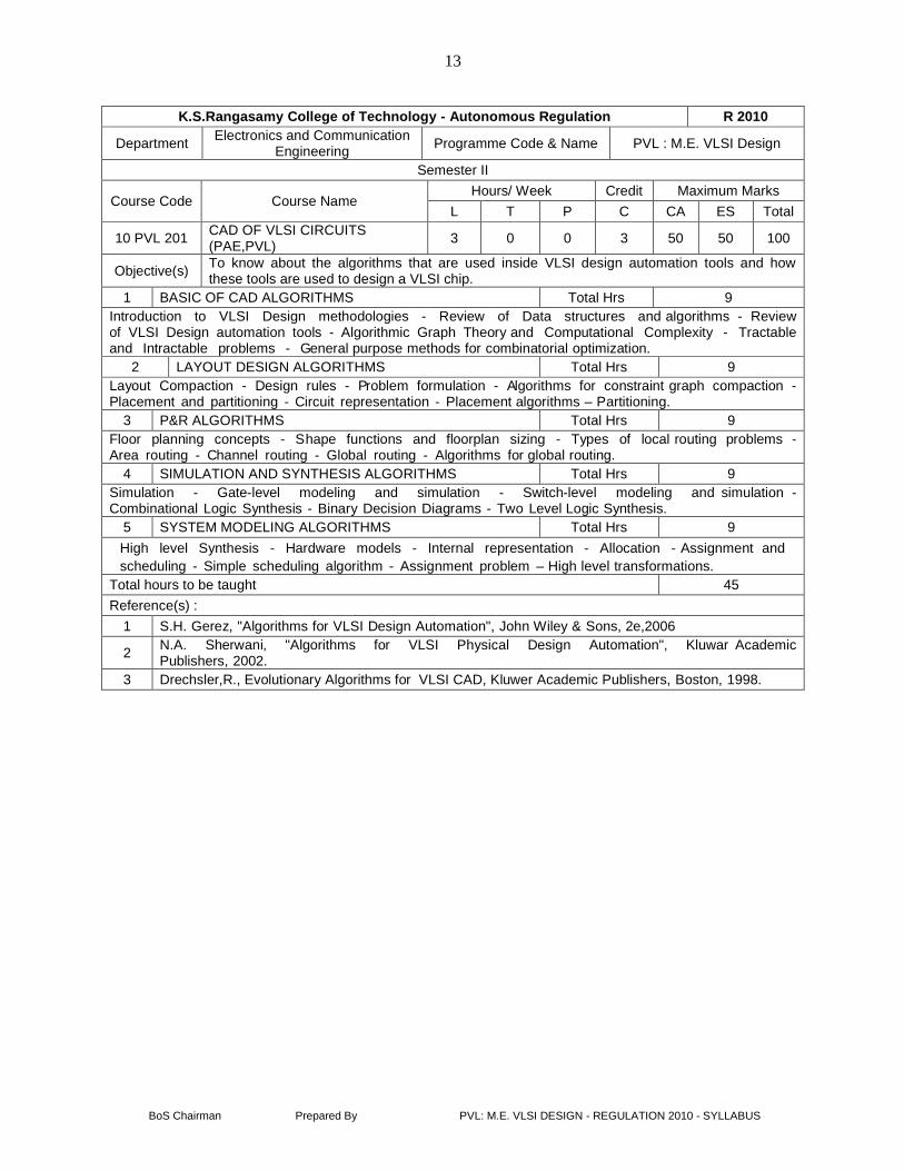
10 PVL 201 CAD OF VLSI CIRCUITS(PAE,PVL) 3 0 0 3 50 50 100
Objective(s) To know about the algorithms that are used inside VLSI design automation tools and howthese tools are used to design a VLSI chip.
1 BASIC OF CAD ALGORITHMS Total Hrs 9Introduction to VLSI Design methodologies - Review of Data structures and algorithms - Reviewof VLSI Design automation tools - Algorithmic Graph Theory and Computational Complexity - Tractableand Intractable problems - General purpose methods for combinatorial optimization.
2 LAYOUT DESIGN ALGORITHMS Total Hrs 9Layout Compaction - Design rules - Problem formulation - Algorithms for constraint graph compaction -Placement and partitioning - Circuit representation - Placement algorithms – Partitioning.
3 P&R ALGORITHMS Total Hrs 9Floor planning concepts - Shape functions and floorplan sizing - Types of local routing problems -Area routing - Channel routing - Global routing - Algorithms for global routing.
4 SIMULATION AND SYNTHESIS ALGORITHMS Total Hrs 9Simulation - Gate-level modeling and simulation - Switch-level modeling and simulation -Combinational Logic Synthesis - Binary Decision Diagrams - Two Level Logic Synthesis.
5 SYSTEM MODELING ALGORITHMS Total Hrs 9High level Synthesis - Hardware models - Internal representation - Allocation - Assignment andscheduling - Simple scheduling algorithm - Assignment problem – High level transformations.
Total hours to be taught 45Reference(s) :
1 S.H. Gerez, "Algorithms for VLSI Design Automation", John Wiley & Sons, 2e,2006
2 N.A. Sherwani, "Algorithms for VLSI Physical Design Automation", Kluwar AcademicPublishers, 2002.
3 Drechsler,R., Evolutionary Algorithms for VLSI CAD, Kluwer Academic Publishers, Boston, 1998.

14
BoS Chairman Prepared By PVL: M.E. VLSI DESIGN - REGULATION 2010 - SYLLABUS
K.S.Rangasamy College of Technology - Autonomous Regulation R 2010
Department Electronics and CommunicationEngineering Programme Code & Name PVL : M.E. VLSI Design
Semester II
Course Code Course NameHours/ Week Credit Maximum Marks
L T P C CA ES Total
10 PVL 202 ANALOG VLSI CIRCUITS(PAE,PVL) 3 0 0 3 50 50 100
Objective(s) To know about the various analog VLSI circuits, DFT and analog VLSI interconnects.1 ANALOG CIRCUIT BUILDING BLOCKS Total Hrs 9
Switches, active resistors - Current sources and sinks - Current mirrors/amplifiers - Voltage and currentreferences, Comparator, Multiplier.
2 AMPLIFIERS Total Hrs 9MOS and BJT inverting amplifier - Improving performance of inverting amplifier - CMOS and BJT differentialamplifiers - Characterization of Op-Amp - The BJT two stage op-amp - The CMOS two stage op-amp - Op-amps with output stage, Folded Cascode op-amp, Transconductance Amplifier.
3 FILTERS Total Hrs 9Low pass filters - High pass filters – Band Pass filters – Phase Locked Loops.
4 DATA CONVERTER FUNDAMENTALS Total Hrs 9Ideal A/D and D/A converters, Quantization noise, Signed codes, Performance limitations.
5 DESIGN FOR TESTABILITY AND ANALOG VLSIINTERCONNECTS Total Hrs 9
Fault modeling and simulation – Testability- Analysis Technique-Ad Hoc Methods and General Guidelines-ScanTechniques-Boundary Scan-Built-in Self Test Analog Test Buses-Design for Electron-Beam Testability-Physicsof Interconnects in VLSI-Scaling of Interconnects-A Model for Estimating wiring Density-A ConfigurableArchitecture for Prototyping Analog Circuits.Total hours to be taught 45Reference(s) :
1 Randall L. Geiger, Phillip E. Allen, Noel R. Strader, "VLSI Design Techniques for Analog and DigitalCircuits", McGraw Hill, International Edition 1990
2 Mohammed Ismail, Terri Fiez, “ Analog VLSI signal and Information Processing”, McGraw-HillInternational Editions, 1994
3 David A. Johns, Ken Martin, “Analog Integrated Circuit Design” John Wiley & Sons, 2002

15
BoS Chairman Prepared By PVL: M.E. VLSI DESIGN - REGULATION 2010 - SYLLABUS
K.S.Rangasamy College of Technology - Autonomous Regulation R 2010
Department Electronics and CommunicationEngineering
Programme Code &Name PVL : M.E. VLSI Design
Semester II
Course Code Course NameHours/ Week Credit Maximum MarksL T P C CA ES Total
10 PVL 203
ADVANCED COMPUTERARCHITECTURE AND PARALLELPROCESSING(PAE,PVL)
3 0 0 3 50 50 100
Objective(s)To understand the basics of parallel processing and Mechanisms used in parallelProcessing. To discuss in detail the principle and classification of pipeline processors. ToStudy the software and parallel programming concepts.
1 THEORY OF PARALLELISM Total Hrs 9Parallel computer models - the state of computing, Multiprocessors and Multicomputer and Multivectors andSIMD computers, PRAM and VLSI models, Architectural development tracks. Program and network properties-Conditions of parallelism.
2 PARTITIONING AND SCHEDULING Total Hrs 9Program partitioning and scheduling, Program flow mechanisms, System interconnect architectures. Principlesof scalable performance - performance matrices and measures, Parallel processing applications, speedupperformance laws, scalability analysis and approaches.
3 HARDWARE TECHNOLOGIES Total Hrs 9Processor and memory hierarchy advanced processor technology, superscalar and vector processors, memoryhierarchy technology, virtual memory technology- Bus Cache and Shared Memory - backplane bus systems,cache memory organizations, shared memory organizations, sequential and weak consistency models,Pipelining and superscalar Techniques.
4 PARALLEL AND SCALABLE ARCHITECTURE Total Hrs 9Multiprocessor and Multicomputer, Multivector and SIMD computers, Scalable, Multithreaded and data flowarchitectures.
5 SOFTWARE AND PARALLEL PROGRAMMING Total Hrs 9Parallel models, Languages and compilers, Parallel program development and environments, UNIX, MACHand OSF/1 for parallel computersTotal hours to be taught 45Reference(s) :
1 Kai Hwang, “Advanced Computer Architecture ", McGraw Hill International, 2001.
2 Dezso Sima, Terence Fountain, Peter Kacsuk, ”Advanced Computer architecture – A Design SpaceApproach”, Pearson Education, 2003.
3 John P.Shen, “Modern processor design. Fundamentals of super scalar processors”, Tata McGraw Hill2003.

16
BoS Chairman Prepared By PVL: M.E. VLSI DESIGN - REGULATION 2010 - SYLLABUS
K.S.Rangasamy College of Technology - Autonomous Regulation R 2010
Department Electronics and CommunicationEngineering Programme Code & Name PVL : M.E. VLSI Design
Semester II
Course Code Course NameHours/ Week Credit Maximum Marks
L T P C CA ES Total10 PVL 204 ASIC DESIGN 3 0 0 3 50 50 100Objective(s) To learn the internal architecture ,types and construction of ASICs
1 INTRODUCTION TO ASICS, CMOS LOGIC AND ASICLIBRARY DESIGN Total Hrs 9
Types of ASICs - Design flow - CMOS transistors - CMOS Design rules - Combinational Logic Cell – Sequentiallogic cell - Data path logic cell - Transistors as Resistors - Transistor Parasitic Capacitance- Logical effort –Librarycell design - Library architecture.
2 PROGRAMMABLE ASICS, PROGRAMMABLE ASIC LOGICCELLS AND PROGRAMMABLE ASIC I/O CELLS Total Hrs 9
Anti fuse - Static RAM - EPROM and EEPROM technology - PREP benchmarks - Actel ACT - Xilinx LCA –AlteraFLEX - Altera MAX DC & AC inputs and outputs - Clock & Power inputs - Xilinx I/O blocks.
3PROGRAMMABLE ASIC INTERCONNECT,PROGRAMMABLE ASIC DESIGN SOFTWARE AND LOWLEVEL DESIGN ENTRY
Total Hrs 9
Actel ACT -Xilinx LCA - Xilinx EPLD – Altera MAX 5000 and 7000 - Altera MAX 9000 - Altera FLEX –Designsystems - Logic Synthesis - Half gate ASIC -Schematic entry - Low level design language - PLA tools -EDIF- CFIdesign representation.
4 LOGIC SYNTHESIS, SIMULATION AND TESTING Total Hrs 9Verilog and logic synthesis -VHDL and logic synthesis - Types of simulation -Boundary scan test - Fault simulation- Automatic test pattern generation.
5 ASIC CONSTRUCTION, FLOOR PLANNING, PLACEMENTAND ROUTING Total Hrs 9
System partition - FPGA partitioning - Partitioning methods - Floor planning - Placement - Physical design flow –Global routing - Detailed routing - Special routing - Circuit extraction - DRC.Total hours to be taught 45Reference(s) :
1 M.J.S .Smith, "Application Specific Integrated Circuits, Pearson Education, 2010.
2 Farzad Nekoogar and Faranak Nekoogar, From ASICs to SOCs: A Practical Approach, Prentice Hall PTR,2003.
3 Wayne Wolf, FPGA-Based System Design, Prentice Hall PTR, 2004.

17
BoS Chairman Prepared By PVL: M.E. VLSI DESIGN - REGULATION 2010 - SYLLABUS
K.S.Rangasamy College of Technology - Autonomous Regulation R 2010
Department Electronics and CommunicationEngineering Programme Code & Name PVL : M.E. VLSI Design
Semester II
Course Code Course NameHours/ Week Credit Maximum Marks
L T P C CA ES Total
10 PVL 205VLSI DESIGN ANDIMPLEMENTATIONLABORATORY
0 0 3 2 50 50 100
Objective(s) To study the designing of various VLSI circuits and its implementation using FPGA.LIST OF EXPERIMENTS
1. Implementation of ALU /MAC unit in FPGA.2. Implementation of 4 bit sliced processor in FPGA.3. Implementation of Real time clock in FPGA.4. Implementation of 3way junction traffic using in FPGA.5. Implementation of sequential Detector using state diagram and in FPGA6. Implementation of IP core with ALU, MAC and logic operation in Xilinx FPGAs .7. Implementation of PLL using FPGA8. TTL design and simulation using Tanner EDA Tool.9. Layout design and simulation of Logic circuits in L&S.
10. DC operating point and transient analysis of TTL Spice netlist. .
18
BoS Chairman Prepared By PVL: M.E. VLSI DESIGN - REGULATION 2010 - SYLLABUS
K.S.Rangasamy College of Technology - Autonomous Regulation R 2010
Department Electronics and CommunicationEngineering Programme Code & Name PVL : M.E. VLSI
DesignSemester II
Course Code Course NameHours / Week Credit Maximum MarksL T P C CA ES Total
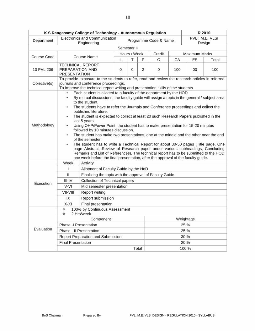
10 PVL 206TECHNICAL REPORTPREPARATION ANDPRESENTATION
0 0 2 0 100 00 100
Objective(s)To provide exposure to the students to refer, read and review the research articles in referredjournals and conference proceedings.To Improve the technical report writing and presentation skills of the students.
Methodology
• Each student is allotted to a faculty of the department by the HOD• By mutual discussions, the faculty guide will assign a topic in the general / subject area
to the student.• The students have to refer the Journals and Conference proceedings and collect the
published literature.• The student is expected to collect at least 20 such Research Papers published in the
last 5 years.• Using OHP/Power Point, the student has to make presentation for 15-20 minutes
followed by 10 minutes discussion.• The student has make two presentations, one at the middle and the other near the end
of the semester.• The student has to write a Technical Report for about 30-50 pages (Title page, One
page Abstract, Review of Research paper under various subheadings, ConcludingRemarks and List of References). The technical report has to be submitted to the HODone week before the final presentation, after the approval of the faculty guide.
Execution
Week ActivityI Allotment of Faculty Guide by the HoDII Finalizing the topic with the approval of Faculty Guide
III-IV Collection of Technical papersV-VI Mid semester presentation
VII-VIII Report writingIX Report submission
X-XI Final presentation
Evaluation
100% by Continuous Assessment 2 Hrs/week
Component WeightagePhase -I Presentation 25 %Phase - II Presentation 25 %Report Preparation and Submission 30 %Final Presentation 20 %
Total 100 %
19
BoS Chairman Prepared By PVL: M.E. VLSI DESIGN - REGULATION 2010 - SYLLABUS
K.S.Rangasamy College of Technology - Autonomous Regulation R 2010
Department Electronics andCommunication Engineering Programme Code & Name PVL : M.E. VLSI Design
Semester III
Course Code Course NameHours/ Week Credit Maximum Marks
L T P C CA ES Total
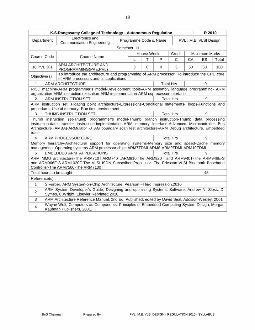
10 PVL 301 ARM ARCHITECTURE ANDPROGRAMMING(PAE,PVL) 3 0 0 3 50 50 100
Objective(s) To introduce the architecture and programming of ARM processor. To introduce the CPU coreof ARM processors and its applications
1 ARM ARCHITECTURE Total Hrs 9RISC machine-ARM programmer’s model-Development tools-ARM assembly language programming- ARMorganization-ARM instruction execution-ARM implementation-ARM coprocessor interface
2 ARM INSTRUCTION SET Total Hrs 9ARM instruction set. Floating point architecture-Expressions-Conditional statements- loops-Functions andprocedures-Use of memory- Run time environment
3 THUMB INSTRUCTION SET Total Hrs 9Thumb instruction set-Thumb programmer’s model-Thumb branch instruction-Thumb data processinginstruction-data transfer instruction-implementation.ARM memory interface-Advanced Microcontroller BusArchitecture (AMBA)-ARMulator -JTAG boundary scan test architecture-ARM Debug architecture. Embeddedtrace.
4 ARM PROCESSOR CORE Total Hrs 9Memory hierarchy-Architectural support for operating systems-Memory size and speed-Cache memorymanagement-Operating systems-ARM processor chips.ARM7TDMI-ARM8-ARM9TDMI-ARM10TDMI
5 EMBEDDED ARM APPLICATIONS Total Hrs 9ARM MMU architecture-The ARM710T.ARM740T.ARM810.The ARM920T and ARM940T-The ARM946E-Sand ARM966E-S.ARM1020E-The VLSI ISDN Subscriber Processor. The Ericsson-VLSI Bluetooth BasebandController-The ARM7500-The ARM7100Total hours to be taught 45Reference(s) :
1 S.Furber, ARM System-on-Chip Architecture, Pearson –Third Impression,2010
2 ARM System Developer’s Guide, Designing and optimizing Systems Software: Andrew N. Sloss, D.Symes, C.Wright, Elsevier Reprinted 2010.
3 ARM Architecture Reference Manual, 2nd Ed, Published, edited by David Seal, Addison-Wesley, 2001
4 Wayne Wolf, Computers as Components: Principles of Embedded Computing System Design, MorganKaufman Publishers, 2001.

20
BoS Chairman Prepared By PVL: M.E. VLSI DESIGN - REGULATION 2010 - SYLLABUS
K.S.Rangasamy College of Technology - Autonomous Regulation R 2010
Department Electronics andCommunication Engineering Programme Code & Name PVL : M.E. VLSI Design
Semester IIICourse Code
Course NameHours/ Week Credit Maximum Marks
L T P C CA ES Total
10 PVL 302 PROJECT WORK –PHASE I 0 0 12 2 100 00 100
Objective (s)To impart the practical knowledge to the students and also to make them to carry out thetechnical procedures in their project work. To provide an exposure to the students to refer,read and review the research articles, journals and conference proceedings relevant to theirproject work and placing this as their beginning stage for their final presentation.
Methodology
• Three reviews have to be conducted by the committee of minimum of three members
one of which should be the guide
• Problem should be selected
• Students have to collect about 20 papers related to their work.
• Report has to be prepared by the students as per the format
• Preliminary implementation can be done if possible
• Internal evaluation has to be done for 100 marks

21
BoS Chairman Prepared By PVL: M.E. VLSI DESIGN - REGULATION 2010 - SYLLABUS
K.S.Rangasamy College of Technology - Autonomous Regulation R 2010
Department Electronics and CommunicationEngineering Programme Code & Name PVL : M.E. VLSI Design
Semester IV
Course Code Course NameHours/ Week Credit Maximum Marks
L T P C CA ES Total
10 PVL 401 PROJECT WORK – PHASE II 0 0 40 10 50 50 100
Objective (s)This enables and strengthens the students to carry out the project on their own and toimplement their innovative ideas to forefront the risk issues and to retrieve the hazards byadopting suitable assessment methodologies and stating it to global.
Methodology
• Three reviews have to be conducted by the committee of minimum of three members
one of which should be the guide
• Each review has to be evaluated for 100 marks.
• Attendance is compulsory for all reviews. If a student fails to attend review for some
valid reason, one or more chance may be given.
• They should publish the paper preferably in the journals/conferences.
• Final review will be done by the committee that consists of minimum of three members
one of which should be the guide (including one external expert examiner)
• The report should be submitted by the students around at the end of May.

22
BoS Chairman Prepared By PVL: M.E. VLSI DESIGN - REGULATION 2010 - SYLLABUS
K.S.Rangasamy College of Technology - Autonomous Regulation R 2010
Department Electronics andCommunication Engineering Programme Code & Name PVL : M.E. VLSI Design
ELECTIVE
Course Code Course NameHours/ Week Credit Maximum Marks
L T P C CA ES Total10 PVL E01 NANO ELECTRONICS 3 0 0 3 50 50 100
Objective(s) To understand the concept about Nano structures, logic devices and data transmission,interfaces and displays.
1 TECHNOLOGY AND ANALYSIS Total Hrs 9Film Deposition Methods – Lithography – Material removing techniques – Etching and Chemical – MechanicalPolishing – Scanning Probe Techniques.
2 CARBON NANO STRUCTURES Total Hrs 9Carbon Clusters – Carbon Nano tubes – Fabrication – Electrical, Mechanical and Vibrational Properties-Applications of Carbon Nano tubes.
3 LOGIC DEVICES Total Hrs 9Silicon MOSFET’s – Novel materials and alternative concepts - Ferroelectric Field Effect Transistors – Superconductor digital electronics – Carbon Nano tubes for data processing.
4 RANDOM ACCESS MEMORIES AND MASS STORAGEDEVICES Total Hrs 9
High Permittivity materials for DRAM’s – Ferro electric Random Access Memories - Magneto-resistive RAM.Hard Disk Drives – Magneto Optical Disks – Rewritable DVDs based on Phase Change Materials –Holographic Data Storage.
5 DATA TRANSMISSION AND INTERFACES AND DISPLAYS Total Hrs 9Photonic Networks – Microwave Communication Systems. Liquid Crystal Displays – Organic Light emittingDevices.Total hours to be taught 45Reference(s) :
1 Rainer Waser ,“Nano Electronics and Information Technology “, Wiley VCH – Feb 20052 Charles Poole ,’Introduction to Nano Technology” Wiley Interscience – May 2003
23
BoS Chairman Prepared By PVL: M.E. VLSI DESIGN - REGULATION 2010 - SYLLABUS
K.S.Rangasamy College of Technology - Autonomous Regulation R 2010
Department Electronics and CommunicationEngineering
Programme Code &Name PVL : M.E. VLSI Design
ELECTIVE
Course Code Course NameHours/ Week Credit Maximum Marks
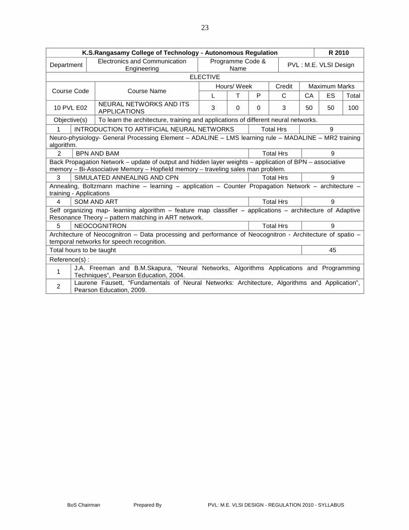
L T P C CA ES Total
10 PVL E02 NEURAL NETWORKS AND ITSAPPLICATIONS 3 0 0 3 50 50 100
Objective(s) To learn the architecture, training and applications of different neural networks.1 INTRODUCTION TO ARTIFICIAL NEURAL NETWORKS Total Hrs 9
Neuro-physiology- General Processing Element – ADALINE – LMS learning rule – MADALINE – MR2 trainingalgorithm.
2 BPN AND BAM Total Hrs 9Back Propagation Network – update of output and hidden layer weights – application of BPN – associativememory – Bi-Associative Memory – Hopfield memory – traveling sales man problem.
3 SIMULATED ANNEALING AND CPN Total Hrs 9Annealing, Boltzmann machine – learning – application – Counter Propagation Network – architecture –training - Applications
4 SOM AND ART Total Hrs 9Self organizing map- learning algorithm – feature map classifier – applications – architecture of AdaptiveResonance Theory – pattern matching in ART network.
5 NEOCOGNITRON Total Hrs 9Architecture of Neocognitron – Data processing and performance of Neocognitron - Architecture of spatio –temporal networks for speech recognition.Total hours to be taught 45Reference(s) :
1 J.A. Freeman and B.M.Skapura, “Neural Networks, Algorithms Applications and ProgrammingTechniques”, Pearson Education, 2004.
2 Laurene Fausett, “Fundamentals of Neural Networks: Architecture, Algorithms and Application”,Pearson Education, 2009.
24
BoS Chairman Prepared By PVL: M.E. VLSI DESIGN - REGULATION 2010 - SYLLABUS
K.S.Rangasamy College of Technology - Autonomous Regulation R 2010
Department Electronics and CommunicationEngineering Programme Code & Name PVL : M.E. VLSI Design
ELECTIVE
Course Code Course NameHours/ Week Credit Maximum Marks
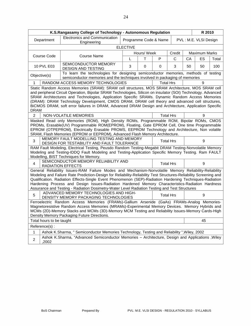
L T P C CA ES Total
10 PVL E03 SEMICONDUCTOR MEMORYDESIGN AND TESTING 3 0 0 3 50 50 100
Objective(s) To learn the technologies for designing semiconductor memories, methods of testingsemiconductor memories and the techniques involved in packaging of memories
1 RANDOM ACCESS MEMORY TECHNOLOGIES Total Hrs 9Static Random Access Memories (SRAM): SRAM cell structures, MOS SRAM Architecture, MOS SRAM celland peripheral Circuit Operation, Bipolar SRAM Technologies, Silicon on insulator (SOI) Technology. AdvancedSRAM Architectures and Technologies, Application Specific SRAMs. Dynamic Random Access Memories(DRAM): DRAM Technology Development, CMOS DRAM, DRAM cell theory and advanced cell structures,BiCMOS DRAM, soft error failures in DRAM, Advanced DRAM Design and Architecture, Application SpecificDRAM
2 NON-VOLATILE MEMORIES Total Hrs 9Masked Read only Memories (ROM), High Density ROMs, Programmable ROM, Bipolar ROMs, CMOSPROMs, Erasable(UV) Programmable ROM(EPROM), Floating, Gate EPROM Cell, One time ProgrammableEPROM (OTPEPROM), Electrically Erasable PROMS, EEPROM Technology and Architecture, Non volatileSRAM, Flash Memories (EPROM or EEPROM), Advanced Flash Memory Architecture.
3 MEMORY FAULT MODELLING TESTING AND MEMORYDESIGN FOR TESTABILITY AND FAULT TOLERANCE Total Hrs 9
RAM Fault Modeling, Electrical Testing, Peusdo Random Testing-Megabit DRAM Testing-Nonvolatile MemoryModeling and Testing-IDDQ Fault Modeling and Testing-Application Specific Memory Testing. Ram FAULTModelling, BIST Techniques for Memory.
4 SEMICONDUCTOR MEMORY RELIABILITY ANDRADIATION EFFECTS Total Hrs 9
General Reliability Issues-RAM Failure Modes and Mechanism-Nonvolatile Memory Reliability-ReliabilityModeling and Failure Rate Prediction-Design for Reliability-Reliability Test Structures-Reliability Screening andQualification. Radiation Effects-Single Event Phenomenon (SEP)-Radiation Hardening Techniques-RadiationHardening Process and Design Issues-Radiation Hardened Memory Characteristics-Radiation HardnessAssurance and Testing - Radiation Dosimetry-Water Level Radiation Testing and Test Structures
5 ADVANCED MEMORY TECHNOLOGIES AND HIGH-DENSITY MEMORY PACKAGING TECHNOLOGIES Total Hrs 9
Ferroelectric Random Access Memories (FRAMs)-Gallium Arsenide (GaAs) FRAMs-Analog Memories-Magnetoresistive Random Access Memories (MRAMs)-Experimental Memory Devices. Memory Hybrids andMCMs (2D)-Memory Stacks and MCMs (3D)-Memory MCM Testing and Reliability Issues-Memory Cards-HighDensity Memory Packaging Future Directions.Total hours to be taught 45Reference(s) :
1 Ashok K.Sharma, " Semiconductor Memories Technology, Testing and Reliability ",Wiley, 2002
2 Ashok K.Sharma, “Advanced Semiconductor Memories – Architecture, Design and Applications ,Wiley,2002

25
BoS Chairman Prepared By PVL: M.E. VLSI DESIGN - REGULATION 2010 - SYLLABUS
K.S.Rangasamy College of Technology - Autonomous Regulation R 2010
Department Electronics and CommunicationEngineering Programme Code & Name PVL : M.E. VLSI
DesignELECTIVE
Course Code Course NameHours/ Week Credit Maximum Marks
L T P C CA ES Total10 PVL E04 LOW POWER VLSI DESIGN 3 0 0 3 50 50 100
Objective(s)To emphasize the optimization and trade – off techniques that involve power dissipation, andto highlight the basic principles, methodologies and techniques that are common to CMOSdigital design.
1 POWER DISSIPATION IN CMOS Total Hrs 9Hierarchy of limits of power – Sources of power consumption – Physics of power dissipation in CMOS FETdevices- Basic principle of low power design.
2 POWER OPTIMIZATION Total Hrs 9Logical level power optimization – Circuit level low power design – Circuit techniques for reducing powerconsumption in adders and multipliers.
3 DESIGN OF LOW POWER CMOS CIRCUITS Total Hrs 9Computer Arithmetic techniques for low power systems – Reducing power consumption in memories – Lowpower clock, Interconnect and layout design – Advanced techniques – Special techniques.
4 POWER ESTIMATION Total Hrs 9Power estimation techniques – Logic level power estimation – Simulation power analysis – Probabilistic poweranalysis.
5 SYNTHESIS AND SOFTWARE DESIGN FOR LOW POWER Total Hrs 9Synthesis for low power –Behavioral level transforms- Software design for low power.Total hours to be taught 45Reference(s) :
1 K.Roy and S.C. Prasad , LOW POWER CMOS VLSI circuit design, Wiley, 2000.
2 Dimitrios Soudris, Chirstian Pignet, Costas Goutis, DESIGNING CMOS CIRCUITS FOR LOW POWER,Kluwer,2002.
3 B. Kuo and J.H Lou, Low voltage CMOS VLSI Circuits, Wiley 1999.4 Gary K.Yeap, practical Low Power Digital VLSI Design, Kluwer academic publishers.
5 James B. Kuo, Shin – chia Lin, Low voltage SOI CMOS VLSI Devices and Circuits. John Wiley andsons, inc 2001.

26
BoS Chairman Prepared By PVL: M.E. VLSI DESIGN - REGULATION 2010 - SYLLABUS
K.S.Rangasamy College of Technology - Autonomous Regulation R 2010
Department Electronics and CommunicationEngineering Programme Code & Name PVL : M.E. VLSI Design
ELECTIVE
Course Code Course NameHours/ Week Credit Maximum Marks
L T P C CA ES Total
10 PVL E05 COMPUTATIONAL INTELLIGENTTECHNIQUES 3 0 0 3 50 50 100
Objective(s)To understand the basics of Fuzzy logic and its modeling concepts, fundamentals of neuralnetworks and its learning concepts. To learn the basics of genetic algorithm and its optimizationprinciples.
1 FUZZY LOGIC Total Hrs 9Introduction to Neuro – Fuzzy and soft Computing – Fuzzy Sets – Basic Definition and Terminology –Set-theoretic operations – Member Function Formulation and parameterization – Fuzzy Rules and FuzzyReasoning- Extension principle and Fuzzy Relations – Fuzzy If-Then Rules – Fuzzy Reasoning –Fuzzy Inference Systems – Mamdani Fuzzy Models-Sugeno Fuzzy Models – Tsukamoto FuzzyModels – Input Space Partitioning and Fuzzy Modeling.
2 GENETIC ALGORITHM Total Hrs 9Derivative-based Optimization – Descent Methods – The Method of steepest Descent – ClassicalNewton’s Method – Step Size Determination – Derivative-free Optimization – Genetic Algorithms –Simulated Annealing – Random Search – Downhill Simplex Search.
3 NEURAL NETWORKS Total Hrs 9Introduction -Supervised Learning Neural Networks – Perceptrons - Adaline – Back propagation Multilayerperceptrons Radial Basis Function Networks – Unsupervised Learning and Other Neural Networks –Competitive Learning Networks – Kohonen Self – Organizing Networks – Learning Vector Quantization –Hebbian Learning.
4 NEURO FUZZY MODELING Total Hrs 9Adaptive Neuro-Fuzzy Inference Systems – Architecture – Hybrid Learning Algorithm – learning Methods thatCross-fertilize ANFIS and RBFN – Coactive Neuro-Fuzzy Modeling – Framework – Neuron Functions forAdaptive Networks – Neuro Fuzzy Spectrum.
5 APPLICATIONS Total Hrs 9Printed Character Recognition – Inverse Kinematics Problems – Automobile Fuel Efficiency prediction –Soft Computing for Color Recipe Prediction.Total hours to be taught 45
Reference(s) :1 J.S.R.Jang, C.T.Sun and E.Mizutani, “Neuro-Fuzzy and Soft Computing”, PHI, Pearson Education 2004.
2 Davis E.Goldberg,” Genetic Algorithms: Search, Optimization and Machine Learning” AddisonWesley, N.Y., 1989.
3 S.Rajasekaran and G.A.V.Pai,” Neural Networks, Fuzzy Logic and Genetic Algorithms”, PHI,2003.
4 R.Eberhart, P.Simpson and R.Dobbins,” Computational Intelligence” PC Tools”, AP professional,Boston 1996.

27
BoS Chairman Prepared By PVL: M.E. VLSI DESIGN - REGULATION 2010 - SYLLABUS
K.S.Rangasamy College of Technology - Autonomous Regulation R 2010
Department Electronics and CommunicationEngineering Programme Code & Name PVL : M.E. VLSI
DesignELECTIVE
Course Code Course NameHours/ Week Credit Maximum MarksL T P C CA ES Total
10 PVL E06 DSP PROCESSOR ARCHITECTUREAND PROGRAMMING 3 0 0 3 50 50 100
Objective(s) Introduction to DSP Processors, Architecture of TMS320C5X and TMS320C3X Processor. andintroduction of DSP family processors.
1 FUNDAMENTALS OF PROGRAMMEMABLE DSPs Total Hrs 9Multiplier and Multiplier accumulator – Modified Bus Structures and Memory access in P-DSPs – Multipleaccess memory – Multi-port memory – VLIW architecture- Pipelining – Special Addressing modes in P-DSPs –chip Peripherals.
2 TMS320C5X PROCESSOR Total Hrs 9Architecture – Assembly language syntax - Addressing modes – Assembly language Instructions - Pipelinestructure, Operation – Block Diagram of DSP starter kit – Application Programmes for processing real timesignals.
3 TMS320C3X PROCESSOR Total Hrs 9Architecture – Data formats - Addressing modes – Groups of addressing modes- Instruction sets - Operation –Block Diagram of DSP starter kit – Application Programmes for processing real time signals – Generating andfinding the sum of series, Convolution of two sequences, Filter design.
4 ADSP PROCESSORS Total Hrs 9Architecture of ADSP-21XX and ADSP-210XX series of DSP processors- Addressing modes and assemblylanguage instructions – Application Programmes –Filter design, FFT calculation.
5 ADVANCED PROCESSORS Total Hrs 9Architecture of TMS320C54X: Pipe line operation, Code Composer studio - Architecture of TMS320C6X -Architecture of Motorola DSP563XX – Comparison of the features of DSP family processors.Total hours to be taught 45Reference(s) :
1 B.Venkataramani and M.Bhaskar, “Digital Signal Processors – Architecture, Programming andApplications” – Tata McGraw – Hill Publishing Company Limited. New Delhi, 2nd edition,2003
2 User guides Texas Instrumentation, Analog Devices, Motorola.

28
BoS Chairman Prepared By PVL: M.E. VLSI DESIGN - REGULATION 2010 - SYLLABUS
K.S.Rangasamy College of Technology - Autonomous Regulation R 2010
Department Electronics andCommunication Engineering Programme Code & Name PVL : M.E. VLSI Design
ELECTIVE
Course Code Course NameHours/ Week Credit Maximum Marks
L T P C CA ES Total10 PVL E07 VLSI SIGNAL PROCESSING 3 0 0 3 50 50 100
Objective(s)To study the transformation for high speed using pipelining, retiring and parallel processingtechniques and experience on power reduction transformation for supply voltage reduction,capacitance reduction. To learn area reduction using folding techniques.
1 INTRODUCTION TO DSP SYSTEMS Total Hrs 9Introduction TO DSP Systems – Typical DSP algorithms: Iteration Bound – data flow graph representations,loop bound and iteration bound, Longest path Matrix algorithm: Pipelining and parallel processing – Pipeliningof FIR digital filters, parallel processing, pipelining and parallel processing for low power.
2 RRRETIMING, FOLDING AND UNFOLDING Total Hrs 9Retiming – definitions and properties Retiming techniques: Unfolding – an algorithm for Unfolding, properties ofunfolding, sample period reduction and parallel processing application: Folding – Folding transformation –Register minimizing techniques.
3 FAST CONVOLUTION Total Hrs 9Fast convolution – Cook-Took algorithm, modified Cook-Took algorithm, Iterated Convolution – CyclicConvolution: Pipelined and parallel recursive and adaptive filters – inefficient/efficient single channelinterleaving, Look – Ahead pipelining in first – order IIR filters, Look-Ahead pipelining and parallel processing ofIIR filters, pipelined adaptive digital filters.
4 BIT-LEVEL ARITHMETIC ARCHITECTURES AND SYSTOLICARCHITECTURE DESIGN Total Hrs 9
BAIT-Level Arithmetic Architectures-parallel multipliers with sign extension, parallel carry-ripple arraymultipliers, parallel carry-save multiplier, 4x 4 bit Baugh-Wooley carry-save multiplication tabular form andimplementation, design of Lyon’s bit-serial multipliers using Horner’s rule, bit-serial FIR filter, CSDrepresentation, CSD multiplication using Horner’s rule for precision improvement, systolic array designmethodology – FIR systolic Arrays – selection of scheduling vector-matrix multiplication and 2D systolic arraydesign-Systolic design for space representations containing Delays.
5 PROGRAMMEMING DIGITAL SIGNAL PROCESSORS Total Hrs 9Synchronous, Wave and asynchronous pipelining – synchronous pipelining and clocking styles, clock skew inedge-trigged single-phase clocking, two-phase clocking, wave pipelining, asynchronous pipelining bundled dataversus dual rail protocol: Programming Digital Signal Processors - general architecture with importantfeatures.Total hours to be taught 45Reference(s) :
1 Keshab K. Parhi, “VLSI Digital Signal Processing Systems Design and Implementation” Wiley -Inter science, 1999
2 Gary Yeap, “Practical Low Power Digital VLSI Design”, Kluwer Academic Publishers, 1998

29
BoS Chairman Prepared By PVL: M.E. VLSI DESIGN - REGULATION 2010 - SYLLABUS
K.S.Rangasamy College of Technology - Autonomous Regulation R 2010
Department Electronics and CommunicationEngineering Programme Code & Name PVL : M.E. VLSI Design
ELECTIVE
Course Code Course NameHours/ Week Credit Maximum Marks
L T P C CA ES Total10 PVL E08 MEMS SYSTEM DESIGN 3 0 0 3 50 50 100
Objective(s) To study the fundamentals of MEMS systems, Materials for Microsystems, fabrication process,system design and micro sensors
1 INTRODUCTION Total Hrs 9Overview – Mems and micro system products – Microsystems and Microelectronics – Working Principle ofMicrosystems – Micro actuation techniques.
2 MATERIALS FOR MICRO SYSTEMS Total Hrs 9Substrate and wafer – single crystal silicon wafer formation – ideal substrates – Mechanical properties – siliconcompounds – Sio2, SiC, Si3N4 and polycrystalline silicon – Silicon piezo resistors – Gallium arsenide, quartz –Piezoelectric crystals - polymers.
3 MICRO SYSTEM FABRICATION PROCESS Total Hrs 9Photolithography – Ion implantation – Diffusion – oxidation – CVD – physical vapor deposition- Deposition byepitaxy – etching process
4 MICRO SYSTEM DESIGN Total Hrs 9Design considerations- Process design- mask layout design – Design constraints – Selection of Materials –Manufacturing Process, Signal transduction – packaging – Application of Micro system in automotive industry– Biomedical – Aerospace - telecommunication
5 MICRO SENSORS Total Hrs 9Introduction – Microsensors – Biomedical sensors – Pressure sensors – Thermal Sensors – Chemical sensors– Optical sensors – Microactuatioan – Mems with actuators.Total hours to be taught 45Reference(s) :
1 Tai-Ran Hus, MEMS & Microsystems Design and Manufacture, Tata McGraw-Hill, 2006.2 Mohamed Gad-el-Hak, The MEMS Hand book, CRC press 2002.
3 Julian W.Gardner, Vijay K.Varadan, Osama O.Awadel Karim, Microsensors MEMS and Smart Devices,John Wiby &sons Ltd.,2001.
4 S.Fatikow, U.Rembold, Microsystem Technology and Microrobotics, Springer-Verlag Berlin Heideiberg,1997.
30
BoS Chairman Prepared By PVL: M.E. VLSI DESIGN - REGULATION 2010 - SYLLABUS
K.S.Rangasamy College of Technology - Autonomous Regulation R 2010
Department Electronics andCommunication Engineering Programme Code & Name PVL : M.E. VLSI Design
ELECTIVE
Course Code Course NameHours/ Week Credit Maximum Marks
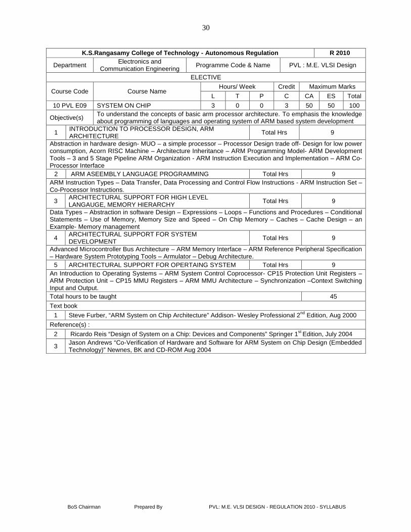
L T P C CA ES Total10 PVL E09 SYSTEM ON CHIP 3 0 0 3 50 50 100
Objective(s) To understand the concepts of basic arm processor architecture. To emphasis the knowledgeabout programming of languages and operating system of ARM based system development
1 INTRODUCTION TO PROCESSOR DESIGN, ARMARCHITECTURE Total Hrs 9
Abstraction in hardware design- MUO – a simple processor – Processor Design trade off- Design for low powerconsumption, Acorn RISC Machine – Architecture Inheritance – ARM Programming Model- ARM DevelopmentTools – 3 and 5 Stage Pipeline ARM Organization - ARM Instruction Execution and Implementation – ARM Co-Processor Interface
2 ARM ASEEMBLY LANGUAGE PROGRAMMING Total Hrs 9ARM Instruction Types – Data Transfer, Data Processing and Control Flow Instructions - ARM Instruction Set –Co-Processor Instructions.
3 ARCHITECTURAL SUPPORT FOR HIGH LEVELLANGAUGE, MEMORY HIERARCHY Total Hrs 9
Data Types – Abstraction in software Design – Expressions – Loops – Functions and Procedures – ConditionalStatements – Use of Memory, Memory Size and Speed – On Chip Memory – Caches – Cache Design – anExample- Memory management
4 ARCHITECTURAL SUPPORT FOR SYSTEMDEVELOPMENT Total Hrs 9
Advanced Microcontroller Bus Architecture – ARM Memory Interface – ARM Reference Peripheral Specification– Hardware System Prototyping Tools – Armulator – Debug Architecture.
5 ARCHITECTURAL SUPPORT FOR OPERTAING SYSTEM Total Hrs 9An Introduction to Operating Systems – ARM System Control Coprocessor- CP15 Protection Unit Registers –ARM Protection Unit – CP15 MMU Registers – ARM MMU Architecture – Synchronization –Context SwitchingInput and Output.Total hours to be taught 45Text book
1 Steve Furber, “ARM System on Chip Architecture” Addison- Wesley Professional 2nd Edition, Aug 2000Reference(s) :
2 Ricardo Reis “Design of System on a Chip: Devices and Components” Springer 1st Edition, July 2004
3 Jason Andrews “Co-Verification of Hardware and Software for ARM System on Chip Design (EmbeddedTechnology)” Newnes, BK and CD-ROM Aug 2004
31
BoS Chairman Prepared By PVL: M.E. VLSI DESIGN - REGULATION 2010 - SYLLABUS
K.S.Rangasamy College of Technology - Autonomous Regulation R 2010
Department Electronics andCommunication Engineering Programme Code & Name PVL : M.E. VLSI Design
ELECTIVE
Course Code Course NameHours/ Week Credit Maximum Marks
L T P C CA ES Total
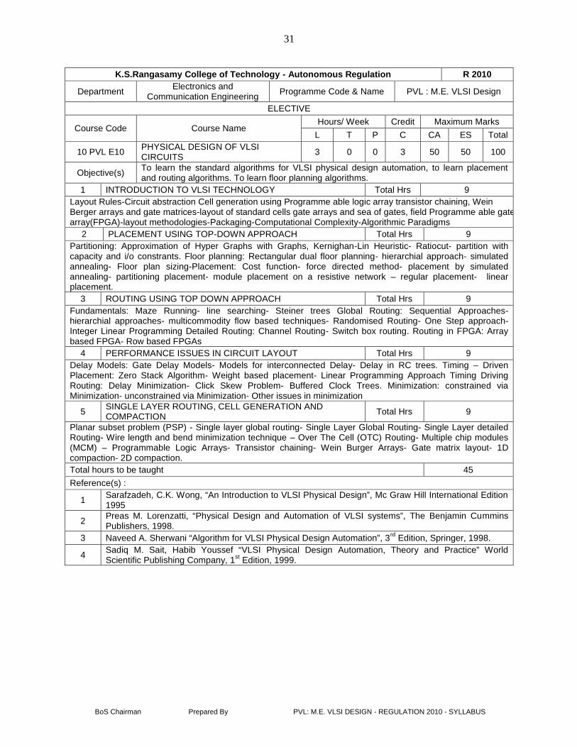
10 PVL E10 PHYSICAL DESIGN OF VLSICIRCUITS 3 0 0 3 50 50 100
Objective(s) To learn the standard algorithms for VLSI physical design automation, to learn placementand routing algorithms. To learn floor planning algorithms.
1 INTRODUCTION TO VLSI TECHNOLOGY Total Hrs 9Layout Rules-Circuit abstraction Cell generation using Programme able logic array transistor chaining, WeinBerger arrays and gate matrices-layout of standard cells gate arrays and sea of gates, field Programme able gatearray(FPGA)-layout methodologies-Packaging-Computational Complexity-Algorithmic Paradigms
2 PLACEMENT USING TOP-DOWN APPROACH Total Hrs 9Partitioning: Approximation of Hyper Graphs with Graphs, Kernighan-Lin Heuristic- Ratiocut- partition withcapacity and i/o constrants. Floor planning: Rectangular dual floor planning- hierarchial approach- simulatedannealing- Floor plan sizing-Placement: Cost function- force directed method- placement by simulatedannealing- partitioning placement- module placement on a resistive network – regular placement- linearplacement.
3 ROUTING USING TOP DOWN APPROACH Total Hrs 9Fundamentals: Maze Running- line searching- Steiner trees Global Routing: Sequential Approaches-hierarchial approaches- multicommodity flow based techniques- Randomised Routing- One Step approach-Integer Linear Programming Detailed Routing: Channel Routing- Switch box routing. Routing in FPGA: Arraybased FPGA- Row based FPGAs
4 PERFORMANCE ISSUES IN CIRCUIT LAYOUT Total Hrs 9Delay Models: Gate Delay Models- Models for interconnected Delay- Delay in RC trees. Timing – DrivenPlacement: Zero Stack Algorithm- Weight based placement- Linear Programming Approach Timing DrivingRouting: Delay Minimization- Click Skew Problem- Buffered Clock Trees. Minimization: constrained viaMinimization- unconstrained via Minimization- Other issues in minimization
5 SINGLE LAYER ROUTING, CELL GENERATION ANDCOMPACTION Total Hrs 9
Planar subset problem (PSP) - Single layer global routing- Single Layer Global Routing- Single Layer detailedRouting- Wire length and bend minimization technique – Over The Cell (OTC) Routing- Multiple chip modules(MCM) – Programmable Logic Arrays- Transistor chaining- Wein Burger Arrays- Gate matrix layout- 1Dcompaction- 2D compaction.Total hours to be taught 45Reference(s) :
1 Sarafzadeh, C.K. Wong, “An Introduction to VLSI Physical Design”, Mc Graw Hill International Edition1995
2 Preas M. Lorenzatti, “Physical Design and Automation of VLSI systems”, The Benjamin CumminsPublishers, 1998.
3 Naveed A. Sherwani “Algorithm for VLSI Physical Design Automation”, 3rd Edition, Springer, 1998.
4 Sadiq M. Sait, Habib Youssef “VLSI Physical Design Automation, Theory and Practice” WorldScientific Publishing Company, 1st Edition, 1999.
32
BoS Chairman Prepared By PVL: M.E. VLSI DESIGN - REGULATION 2010 - SYLLABUS
K.S.Rangasamy College of Technology - Autonomous Regulation R 2010
Department Electronics and CommunicationEngineering Programme Code & Name PVL : M.E. VLSI Design
ELECTIVE
Course Code Course NameHours/ Week Credit Maximum Marks
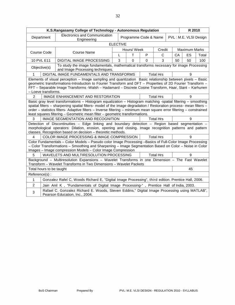
L T P C CA ES Total10 PVL E11 DIGITAL IMAGE PROCESSING 3 0 0 3 50 50 100
Objective(s) To study the image fundamentals, mathematical transforms necessary for image Processingand Image Processing techniques.
1 DIGITAL IMAGE FUNDAMENTALS AND TRANSFORMS Total Hrs 9Elements of visual perception – Image sampling and quantization Basic relationship between pixels – Basicgeometric transformations-Introduction to Fourier Transform and DFT – Properties of 2D Fourier Transform –FFT – Separable Image Transforms -Walsh – Hadamard – Discrete Cosine Transform, Haar, Slant – Karhunen– Loeve transforms.
2 IMAGE ENHANCEMENT AND RESTORATION Total Hrs 9Basic gray level transformations – Histogram equalization – Histogram matching -spatial filtering – smoothingspatial filters – sharpening spatial filters- model of the image degradation / Restoration process- mean filters –order – statistics filters- Adaptive filters – Inverse filtering – minimum mean square error filtering – constrainedleast squares filtering – Geometric mean filter – geometric transformations.
3 IMAGE SEGMENTATION AND RECOGNITION Total Hrs 9Detection of Discontinuities – Edge linking and boundary detection – Region based segmentation –morphological operators: Dilation, erosion, opening and closing. Image recognition patterns and patternclasses. Recognition based on decision – theoretic methods.
4 COLOR IMAGE PROCESSING & IMAGE COMPRESSION Total Hrs 9Color Fundamentals – Color Models – Pseudo color Image Processing –Basics of Full-Color Image Processing– Color Transformations – Smoothing and Sharpening – Image Segmentation Based on Color – Noise in ColorImages – Image compression Models – Color Image Compression
5 WAVELETS AND MULTIRESOLUTION PROCESSING Total Hrs 9Background – Multiresolution Expansions – Wavelet Transforms in one Dimension – The Fast WaveletTransform – Wavelet Transforms in Two Dimensions – Wavelet PacketsTotal hours to be taught 45Reference(s) :
1 Gonzalez Rafel C, Woods Richard E, "Digital Image Processing", third edition. Prentice Hall, 2006.2 Jain Anil K , "Fundamentals of Digital Image Processing-" , Prentice Hall of India, 2003.
3 Rafael C. Gonzalez Richard E. Woods, Steven Eddins,” Digital Image Processing using MATLAB”,Pearson Education, Inc., 2004.

33
BoS Chairman Prepared By PVL: M.E. VLSI DESIGN - REGULATION 2010 - SYLLABUS
K.S.Rangasamy College of Technology - Autonomous Regulation R 2010
Department Electronics andCommunication Engineering Programme Code & Name PVL : M.E. VLSI Design
ELECTIVE
Course Code Course NameHours/ Week Credit Maximum Marks
L T P C CA ES Total10 PVL E12 VLSI TECHNOLOGY 3 0 0 3 50 50 100
Objective(s) To learn methodology for IC fabrication and to learn various techniques are diffusion, ionimplantation, Oxidation, epitaxy, etching, lithography for circuit fabrication.
1 MATERIAL PROPERTIES & CRYSTAL GROWTH Total Hrs 9Crystal structure- axes & planes, Crystal defects-Point defects & dislocations Crystal growth- Bridgman,Czochralski techniques & Zone process, Doping in the melt.
2 DIFFUSION & ION IMPLANTATION Total Hrs 9Nature of diffusion-interstitial, Substitutional, interstitial substitutional movements, Diffusion constant, Dissociateprocess, Diffusion equation- D is constant & function, Diffusion systems, problems in Si Diffusion, EvaluationTechniques Ion Implantation: Penetration range, Implantation Damage, Annealing, ImplantationSystems.
3 OXIDATION & EPITAXY Total Hrs 9OXIDATION: Thermal Oxidation-Intrinsic, Extrinsic silicon Glass, Oxide formation, Kinetics of Oxide growth,Oxidation systems, Faults, Anodic OxidationEPITAXY: Vapour Phase Epitaxy (VPE)- transport, reaction and growth, Chemistry of growth, Insitu etching,Selective epitaxy, imperfections, Liquid Phase Epitaxy, LPE system, Evaluation of epitaxial layers.
4 ETCHING & LITHOGRAPHY Total Hrs 9LITHOGRAPHY: Pattern generation & Masking, Printing & Engraving-Optical, E-Beam, ion Beam, X-Ray,Photoresists, Defects.ETCHING: Wet chemical etching- anisotropic etchants, Etching for non-crystalline films-Plasma etching,Plasma-assisted etching, Cleaning
5 DEVICE & CIRCUIT FABRICATION Total Hrs 9Isolation- Mesa, Oxide, PN-junction isolations, Self Allignment, Local Oxidation, Planarisation, Metallisation andPackaging. Circuits – N, P and CMOS Transistors, Memory devices, BJT Circuits – Buried Layer, PNP andNPN Transistors, Diodes, Resistors, Capacitors.Total hours to be taught 45Reference(s) :
1 Sze S.M. “VLSI Technology “, McGraw Hill, New York, 1983
2 Sorab K. Gandhi “VLSI Fabrication Principles – Silicon and Gallium Arsenide”, Wiley IntersciencePublications, New York 1983, 2nd Edition 1994.
3 Chang S.Y. and S.M. Sze, “VLSI Technology”, McGraw Hill, New York, 1996
34
BoS Chairman Prepared By PVL: M.E. VLSI DESIGN - REGULATION 2010 - SYLLABUS
K.S.Rangasamy College of Technology - Autonomous Regulation R 2010
Department Electronics andCommunication Engineering Programme Code & Name PVL : M.E. VLSI Design
ELECTIVE
Course Code Course NameHours/ Week Credit Maximum Marks
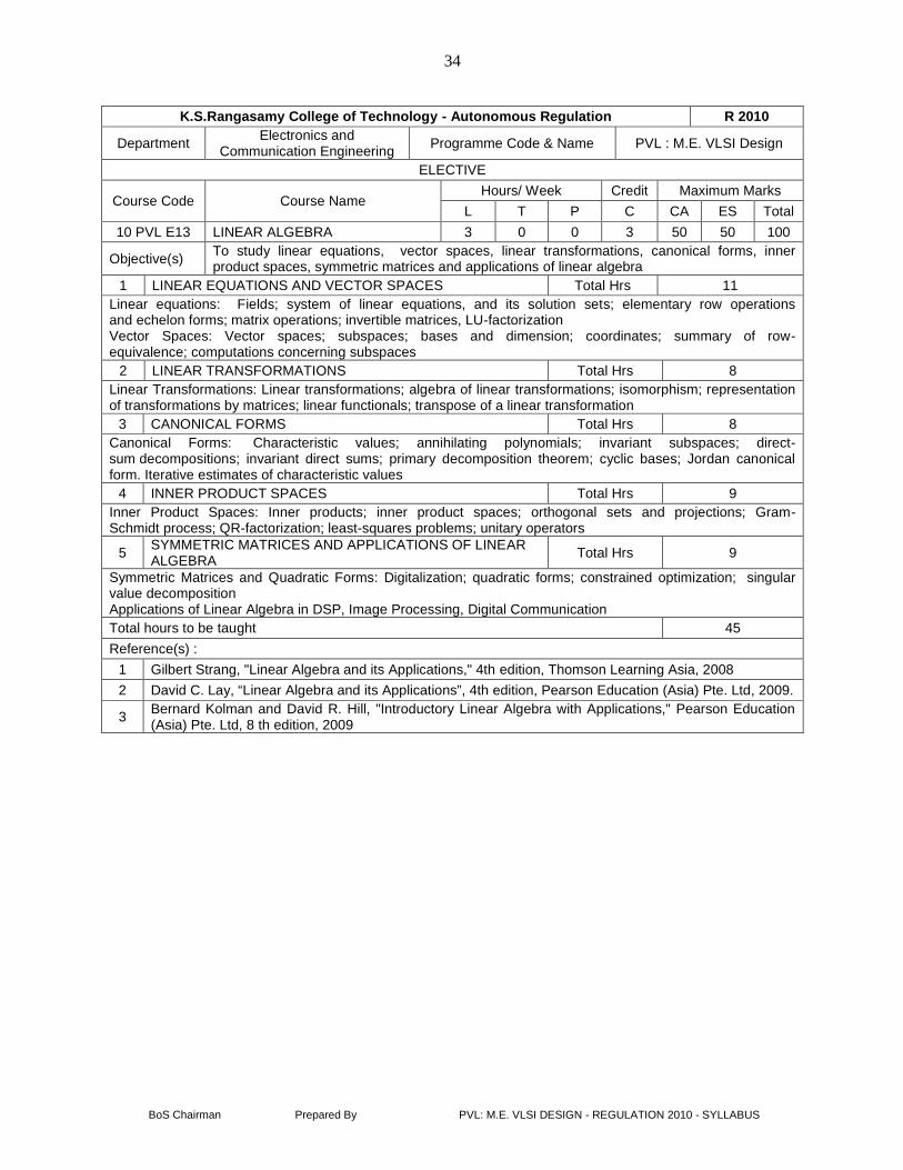
L T P C CA ES Total10 PVL E13 LINEAR ALGEBRA 3 0 0 3 50 50 100
Objective(s) To study linear equations, vector spaces, linear transformations, canonical forms, innerproduct spaces, symmetric matrices and applications of linear algebra
1 LINEAR EQUATIONS AND VECTOR SPACES Total Hrs 11Linear equations: Fields; system of linear equations, and its solution sets; elementary row operationsand echelon forms; matrix operations; invertible matrices, LU-factorizationVector Spaces: Vector spaces; subspaces; bases and dimension; coordinates; summary of row-equivalence; computations concerning subspaces
2 LINEAR TRANSFORMATIONS Total Hrs 8Linear Transformations: Linear transformations; algebra of linear transformations; isomorphism; representationof transformations by matrices; linear functionals; transpose of a linear transformation
3 CANONICAL FORMS Total Hrs 8Canonical Forms: Characteristic values; annihilating polynomials; invariant subspaces; direct-sum decompositions; invariant direct sums; primary decomposition theorem; cyclic bases; Jordan canonicalform. Iterative estimates of characteristic values
4 INNER PRODUCT SPACES Total Hrs 9Inner Product Spaces: Inner products; inner product spaces; orthogonal sets and projections; Gram-Schmidt process; QR-factorization; least-squares problems; unitary operators
5 SYMMETRIC MATRICES AND APPLICATIONS OF LINEARALGEBRA Total Hrs 9
Symmetric Matrices and Quadratic Forms: Digitalization; quadratic forms; constrained optimization; singularvalue decompositionApplications of Linear Algebra in DSP, Image Processing, Digital CommunicationTotal hours to be taught 45Reference(s) :
1 Gilbert Strang, "Linear Algebra and its Applications," 4th edition, Thomson Learning Asia, 20082 David C. Lay, “Linear Algebra and its Applications”, 4th edition, Pearson Education (Asia) Pte. Ltd, 2009.
3 Bernard Kolman and David R. Hill, "Introductory Linear Algebra with Applications," Pearson Education(Asia) Pte. Ltd, 8 th edition, 2009

35
BoS Chairman Prepared By PVL: M.E. VLSI DESIGN - REGULATION 2010 - SYLLABUS
K.S.Rangasamy College of Technology - Autonomous Regulation R 2010
Department Electronics and CommunicationEngineering Programme Code & Name PVL : M.E. VLSI Design
ELECTIVE
Course Code Course NameHours/ Week Credit Maximum Marks
L T P C CA ES Total10 PVL E14 CMOS VLSI DESIGN 3 0 0 3 50 50 100
Objective(s) To learn the CMOS processing technology and basic CMOS circuits, CMOS transistor theoryand to learn logic design.
1 MOS TRANSISTOR THEORY Total Hrs 9Introduction to I.C Technology. Basic MOS transistors. Threshold Voltage. Body effect. Basic D.C. Equations.Second order effects. MOS models. Small signal A.C characteristics. The complementary CMOS inverter. DCcharacteristics. Static Load MOS inverters. The differential inverters. Transmission gate.
2 CMOS PROCESSING TECHNOLOGY Total Hrs 9Silicon semiconductor technology. Wafer processing, Oxidation, epitaxy, deposition, Ion implantation. CMOStechnology. nwell, pwell process, Twin tub processes. Silicon on insulator. CMOS process enhancement.Interconnect and circuit elements. Layout design rules. Latch up.
3 CIRCUIT CHARACTERISTICS AND PERFORMANCEESTIMATION Total Hrs 9
Resistance estimation. Capacitance estimation. MOS capacitor characteristics. Device capacitances. Diffusioncapacitance. SPICE modeling of MOS capacitance. Routing capacitance. Distributed RC effects. Inductance.Switching characteristics. Rise time. Fall time. Delay time. Empirical delay models. Gate delays. CMOS gatetransistor sizing. Power dissipation, Design margining. Scaling of MOS transistor dimensions.
4 CMOS CIRCUIT AND LOGIC DESIGN Total Hrs 9CMOS Logic gate design. Fan in and fan out. Typical CMOS NAND and NOR delays. Transistor sizing. CMOSlogic structures. Complementary logic. BICMOS logic. Pseudo NMOS logic. Dynamic CMOS logic. ClockedCMOS logic. Pass transistor logic. CMOS domino logic. NP domino logic. Cascade voltage switch logic. Sourcefollower pull up Logic (SFPL). Clocking strategies – I/O structures.
5 CMOS SUBSYSTEM DESIGN Total Hrs 9Data path operations. Addition/subtraction. Parity generators. Comparators. Zero/one detectors. BinaryCounters. ALUs. Multiplication. Array, Radix-n, Wallace Tree and Serial Multiplication. Shifters. Memoryelements. RWM, Rom, Content Addressable Memory. Control: FSM, PLA Control Implementation.Total hours to be taught 45Reference(s) :
1 Neil.H.E. Weste and K.Eshragian, “Principles of CMOS VLSI Design”. 2nd Edition. Addison-Wesley,2000.
2 Douglas a. Pucknell and K.Eshragian., “Basic VLSI Design” 3rd Edition. PHI, 2000.3 R. Jacob Baker, Harry W. LI., & David K. Boyce., “CMOS Circuit Design”, 3rd Indian reprint, PHI, 2000.4 John P.Uyemura,”Introduction to VLSI circuits and systems”, john willey and sons, 2010.
36
BoS Chairman Prepared By PVL: M.E. VLSI DESIGN - REGULATION 2010 - SYLLABUS
K.S.Rangasamy College of Technology - Autonomous Regulation R 2010
Department Electronics andCommunication Engineering Programme Code & Name PVL : M.E. VLSI Design
ELECTIVE
Course Code Course NameHours/ Week Credit Maximum Marks
L T P C CA ES Total
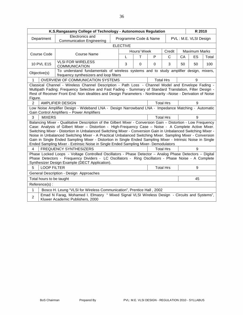
10 PVL E15 VLSI FOR WIRELESSCOMMUNICATION 3 0 0 3 50 50 100
Objective(s) To understand fundamentals of wireless systems and to study amplifier design, mixers,frequency synthesizers and loop filters
1 OVERVIEW OF COMMUNICATION SYSTEMS Total Hrs 9Classical Channel - Wireless Channel Description - Path Loss - Channel Model and Envelope Fading -Multipath Fading: Frequency Selective and Fast Fading - Summary of Standard Translation, Filter Design -Rest of Receiver Front End: Non idealities and Design Parameters - Nonlinearity –Noise - Derivation of NoiseFigure.
2 AMPLIFIER DESIGN Total Hrs 9Low Noise Amplifier Design - Wideband LNA - Design Narrowband LNA - Impedance Matching - AutomaticGain Control Amplifiers – Power Amplifiers
3 MIXERS Total Hrs 9Balancing Mixer - Qualitative Description of the Gilbert Mixer - Conversion Gain – Distortion - Low FrequencyCase: Analysis of Gilbert Mixer – Distortion - High-Frequency Case – Noise - A Complete Active Mixer.Switching Mixer - Distortion in Unbalanced Switching Mixer - Conversion Gain in Unbalanced Switching Mixer -Noise in Unbalanced Switching Mixer - A Practical Unbalanced Switching Mixer. Sampling Mixer - ConversionGain in Single Ended Sampling Mixer - Distortion in Single Ended Sampling Mixer - Intrinsic Noise in SingleEnded Sampling Mixer - Extrinsic Noise in Single Ended Sampling Mixer- Demodulators
4 FREQUENCY SYNTHESIZERS Total Hrs 9Phase Locked Loops - Voltage Controlled Oscillators - Phase Detector – Analog Phase Detectors – DigitalPhase Detectors - Frequency Dividers - LC Oscillators - Ring Oscillators - Phase Noise - A CompleteSynthesizer Design Example (DECT Application).
5 LOOP FILTER Total Hrs 9General Description - Design ApproachesTotal hours to be taught 45Reference(s) :
1 Bosco H. Leung “VLSI for Wireless Communication”, Prentice Hall , 2002
2 Emad N Farag, Mohamed I. Elmasry “ Mixed Signal VLSI Wireless Design - Circuits and Systems”,Kluwer Academic Publishers, 2000
37
BoS Chairman Prepared By PVL: M.E. VLSI DESIGN - REGULATION 2010 - SYLLABUS
K.S.Rangasamy College of Technology - Autonomous Regulation R 2010
Department Electronics andCommunication Engineering Programme Code & Name PVL : M.E. VLSI Design
ELECTIVE
Course Code Course NameHours/ Week Credit Maximum Marks
L T P C CA ES Total10 PVL E16 FPGA - BASED SYSTEM DESIGN 3 0 0 3 50 50 100
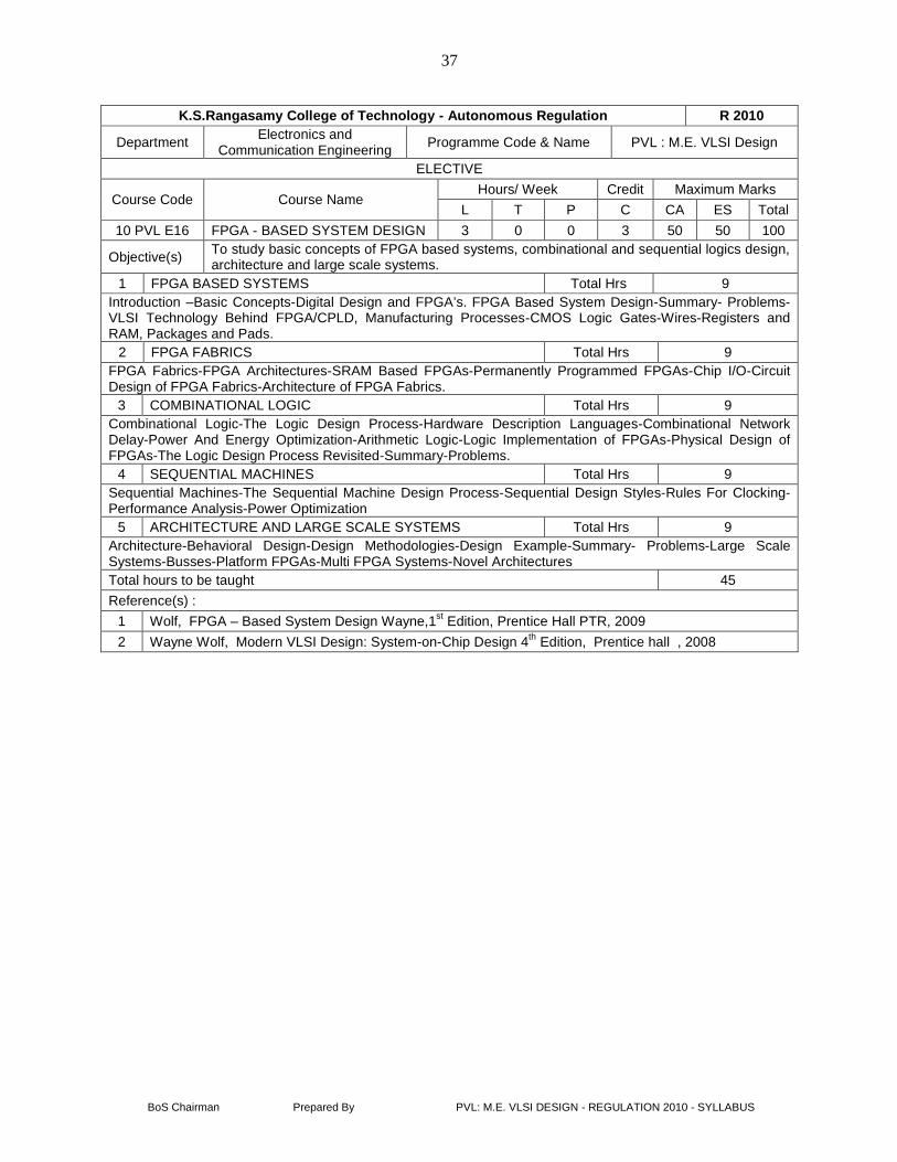
Objective(s) To study basic concepts of FPGA based systems, combinational and sequential logics design,architecture and large scale systems.
1 FPGA BASED SYSTEMS Total Hrs 9Introduction –Basic Concepts-Digital Design and FPGA’s. FPGA Based System Design-Summary- Problems-VLSI Technology Behind FPGA/CPLD, Manufacturing Processes-CMOS Logic Gates-Wires-Registers andRAM, Packages and Pads.
2 FPGA FABRICS Total Hrs 9FPGA Fabrics-FPGA Architectures-SRAM Based FPGAs-Permanently Programmed FPGAs-Chip I/O-CircuitDesign of FPGA Fabrics-Architecture of FPGA Fabrics.
3 COMBINATIONAL LOGIC Total Hrs 9Combinational Logic-The Logic Design Process-Hardware Description Languages-Combinational NetworkDelay-Power And Energy Optimization-Arithmetic Logic-Logic Implementation of FPGAs-Physical Design ofFPGAs-The Logic Design Process Revisited-Summary-Problems.
4 SEQUENTIAL MACHINES Total Hrs 9Sequential Machines-The Sequential Machine Design Process-Sequential Design Styles-Rules For Clocking-Performance Analysis-Power Optimization
5 ARCHITECTURE AND LARGE SCALE SYSTEMS Total Hrs 9Architecture-Behavioral Design-Design Methodologies-Design Example-Summary- Problems-Large ScaleSystems-Busses-Platform FPGAs-Multi FPGA Systems-Novel ArchitecturesTotal hours to be taught 45Reference(s) :
1 Wolf, FPGA – Based System Design Wayne,1st Edition, Prentice Hall PTR, 20092 Wayne Wolf, Modern VLSI Design: System-on-Chip Design 4th Edition, Prentice hall , 2008


![CURRICULUM 2013 M.E - POWER ELECTRONICS AND DRIVES ... · PDF fileKCT-M.E. [PED] 1-4th Semester Curriculum and Syllabus [R: 2013] 6 Signature of the Chairman BOS EEE P13PET101 ADVANCED](https://img.dokumen.tips/doc/110x75/5a9e5a0f7f8b9a077e8c201a/curriculum-2013-me-power-electronics-and-drives-ped-1-4th-semester-curriculum.jpg)