Embed Size (px)
Citation preview

CSEE 3827: Fundamentals of Computer Systems, Spring 2011
3. Combinational Circuit Design
Prof. Martha Kim ([email protected])Web: http://www.cs.columbia.edu/~martha/courses/3827/sp11/

Outline (H&H 2.8, 5.2)
2
• Standard combinational circuits
• Decoder
• Encoder / priority encoder (bonus, not in text)
• Code converter (bonus, not in text)
• Multiplexer
• Addition
• Half and full adders
• Ripple carry adder
• Carry lookahead adder
• Subtraction
• Comparator (“!=” in lecture, “<“ in text)
• ALU (in text, not covering yet)
• Shifter

Combinational circuits
• Combinational circuits are stateless
• The outputs are functions only of the inputs
3
Combinational circuit OutputsInputs

Hierarchical design
4
© 2008 Pearson Education, Inc.M. Morris Mano & Charles R. KimeLOGIC AND COMPUTER DESIGN FUNDAMENTALS, 4e
3-4
(a)
A0 N0MX
MX
MX
MX
ME
N1
N2
N3
E
B0
A1
B1
A2
B2
A3
B3
Ai
Ni
MXBi
N0N1 E
MEN2N3
(b) (c)
Design small circuits to be used in a bigger circuit“Big”Circuit
Smaller Circuits

Hierarchical design (It’s a comparator!)
5
© 2008 Pearson Education, Inc.M. Morris Mano & Charles R. KimeLOGIC AND COMPUTER DESIGN FUNDAMENTALS, 4e
3-4
(a)
A0 N0MX
MX
MX
MX
ME
N1
N2
N3
E
B0
A1
B1
A2
B2
A3
B3
Ai
Ni
MXBi
N0N1 E
MEN2N3
(b) (c)
(4-bit equality comparator)
(NEQ)

Enabler circuits
6
© 2008 Pearson Education, Inc.M. Morris Mano & Charles R. KimeLOGIC AND COMPUTER DESIGN FUNDAMENTALS, 4e
3-15
XF
EN
(a)
ENX
F
(b)
Output is “enabled” (F=A) only when input ‘ENABLE’ signal is asserted (EN=1)
EN F
0 0
1 A
A
A EN F
0 1
1 A

Decoder-based circuits
7
3:8decoder
A
B
C
ABC
ABC
ABC
ABC
ABC
ABC
ABC
ABC
Converts n-bit input to m-bit output, where n <= m <= 2n
“Standard” Decoder: ith output = 1, all others = 0,
where i is the binary representation of the input (ABC)

Decoder-based circuits
7
3:8decoder
A
B
C
ABC
ABC
ABC
ABC
ABC
ABC
ABC
ABC
Converts n-bit input to m-bit output, where n <= m <= 2n
“Standard” Decoder: ith output = 1, all others = 0,
where i is the binary representation of the input (ABC)
e.g., ABC = 101 (i=5)
1
10
00000
00
1
Internal design of 1:2 decoder
8
© 2008 Pearson Education, Inc.M. Morris Mano & Charles R. KimeLOGIC AND COMPUTER DESIGN FUNDAMENTALS, 4e
3-17
A D0 D1
0 1 01 0 1
(a) (b)
D1 AA
D0 A

Internal design of 2:4 decoder
9
© 2008 Pearson Education, Inc.M. Morris Mano & Charles R. KimeLOGIC AND COMPUTER DESIGN FUNDAMENTALS, 4e
3-18
A1
0011
A0
0101
D0
1000
D1
0100
D2
0010
D3
0001
(a)
D0 A1 A0
D1 A1 A0
D2 A1 A0
D3 A1 A0
(b)
A1
A0

Hierarchical design of 2:4 decoder
10
2:4 decoder
1:2
decoder
1:2
decoder
b
a
'b
b
'a
a
'b'a
'ba
b'a
ba
Can build 2:4 decoder out of two 1:2 decoders (and some additional circuitry)

Hierarchical design of 3:8 decoder
11
3:8 decoder
2:4 decoder
b
a
'b'a
'ba
b'a
ba
1:2 decoderc
'c
c
'c'b'a
'c'ba
'cb'a
'cba
c'b'a
c'ba
cb'a
cba

Encoders
12
Inverse of a decoder: converts m-bit input to n-bit output, where n <= m <= 2n
© 2008 Pearson Education, Inc.M. Morris Mano & Charles R. KimeLOGIC AND COMPUTER DESIGN FUNDAMENTALS, 4e
T 3-7
TABLE 3-7Truth Table for Octal-to-Binary Encoder
Inputs Outputs
D7 D6 D5 D4 D3 D2 D1 D0 A2 A1 A0
00000001
00000010
00000100
00001000
00010000
00100000
01000000
10000000
00001111
00110011
01010101

Decoder and encoder summary
13
BCD values One-hot encoding
0 0 0 0 0 0 0 0 0 0 1
0 0 1 0 0 0 0 0 0 1 0
0 1 0 0 0 0 0 0 1 0 0
0 1 1 0 0 0 0 1 0 0 0
1 0 0 0 0 0 1 0 0 0 0
1 0 1 0 0 1 0 0 0 0 0
1 1 0 0 1 0 0 0 0 0 0
1 1 1 1 0 0 0 0 0 0 0
Decoder
Encoder
n}2n{
n{ n}2
Note: for Encoders - input is assumed to have just one 1, the rest 0’s

In class design: priority encoder
14
A priority encoder takes 2^n bit input (I) and produces n bits of output (K) indicating in BCD the position of the most significant 1 on the input.
I3 I2 I1 I0 K1 K0
0 0 0 1 0 0
0 0 1 x 0 1
0 1 x x 1 0
1 x x x 1 1
J3 J2 J1 J0 K1 K0
0 0 0 1 0 0
0 0 1 0 0 1
0 1 0 0 1 0
1 0 0 0 1 1
We will leverage a regular encoder which takes 2^n bit one-hot encoded input (J) and produces n bits of output (K) indicating in BCD the position of the 1 on the input.
PriorityEncoder
I K
EncoderJ K

In class design: priority encoder (2)
15
This gets us part of the way there, leaving us with a simpler problem of translating I into J:
I3 I2 I1 I0 J3 J2 J1 J0
0 0 0 1 0 0 0 1
0 0 1 x 0 0 1 0
0 1 x x 0 1 0 0
1 x x x 1 0 0 0Priority Encoder
I KEncoder
J
?
From inspection of the truth table we can see the following definitions of Jx. Could also have used k-maps.J3 = I3J2 = I2`I3J1 = I1`I2`I3J0 = I0`I1`I2`I3
NB: An input i = x is still a don’t care, it means “for all possible values of i”. So here input 1xxx means any 4-bit input starting with a 1, i.e., 1000, 1001, 1010, 1011, 1100, ...

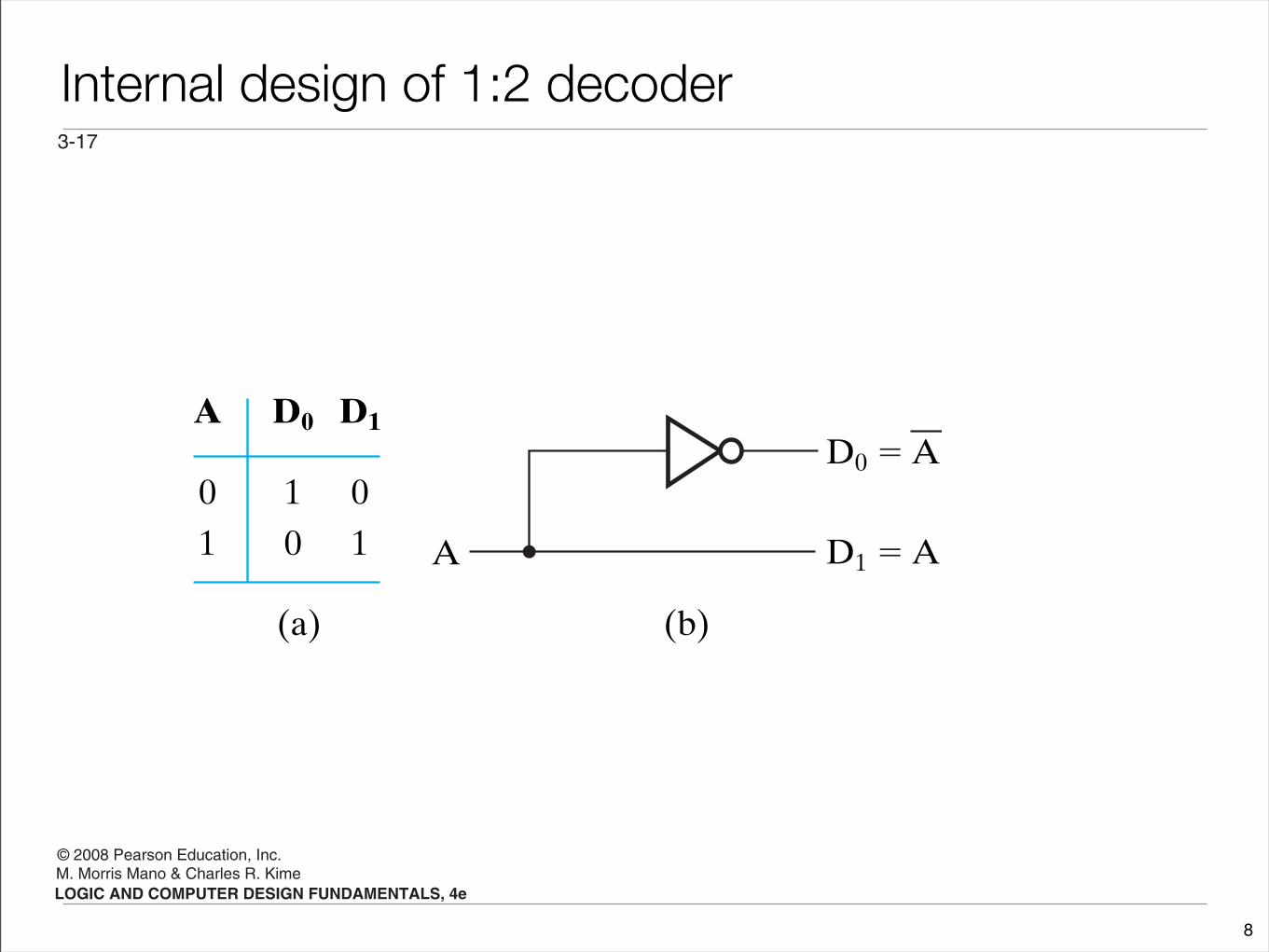
General code conversion
16
© 2008 Pearson Education, Inc.M. Morris Mano & Charles R. KimeLOGIC AND COMPUTER DESIGN FUNDAMENTALS, 4e
3-3
(a) Segment designation
a
bf
e cg
d(b) Numeric designation for display
Code conversion
17
a
bf
e
d
cg
Val
W X Y Z a b c d e f g0 0 0 0 0 1 1 1 1 1 1 01 0 0 0 1 0 1 1 0 0 0 02 0 0 1 0 1 1 0 1 1 0 13 0 0 1 1 1 1 1 1 0 0 14 0 1 0 0 0 1 1 0 0 1 15 0 1 0 1 1 0 1 1 0 1 16 0 1 1 0 1 0 1 1 1 1 17 0 1 1 1 1 1 1 0 0 0 08 1 0 0 0 1 1 1 1 1 1 19 1 0 0 1 1 1 1 0 0 1 1X 1 0 1 0 X X X X X X XX 1 0 1 1 X X X X X X XX 1 1 0 0 X X X X X X XX 1 1 0 1 X X X X X X XX 1 1 1 0 X X X X X X XX 1 1 1 1 X X X X X X X
Input Output

Code conversion
18
a
bf
e
d
cg
Val
W X Y Z a b c d e f g0 0 0 0 0 1 1 1 1 1 1 01 0 0 0 1 0 1 1 0 0 0 02 0 0 1 0 1 1 0 1 1 0 13 0 0 1 1 1 1 1 1 0 0 14 0 1 0 0 0 1 1 0 0 1 15 0 1 0 1 1 0 1 1 0 1 16 0 1 1 0 1 0 1 1 1 1 17 0 1 1 1 1 1 1 0 0 0 08 1 0 0 0 1 1 1 1 1 1 19 1 0 0 1 1 1 1 0 0 1 1X 1 0 1 0 X X X X X X XX 1 0 1 1 X X X X X X XX 1 1 0 0 X X X X X X XX 1 1 0 1 X X X X X X XX 1 1 1 0 X X X X X X XX 1 1 1 1 X X X X X X X
Input Output
e.g., what outputs “lights up” when input
V=4?

Code conversion
19
a
bf
e
d
cg
Val
W X Y Z a b c d e f g0 0 0 0 0 1 1 1 1 1 1 01 0 0 0 1 0 1 1 0 0 0 02 0 0 1 0 1 1 0 1 1 0 13 0 0 1 1 1 1 1 1 0 0 14 0 1 0 0 0 1 1 0 0 1 15 0 1 0 1 1 0 1 1 0 1 16 0 1 1 0 1 0 1 1 1 1 17 0 1 1 1 1 1 1 0 0 0 08 1 0 0 0 1 1 1 1 1 1 19 1 0 0 1 1 1 1 0 0 1 1X 1 0 1 0 X X X X X X XX 1 0 1 1 X X X X X X XX 1 1 0 0 X X X X X X XX 1 1 0 1 X X X X X X XX 1 1 1 0 X X X X X X XX 1 1 1 1 X X X X X X X
Input Output
For what values does output f “light up” for?
1 0 0 0
1 1 0 1
X X X X
1 1 X XW=1
X=1
Y=1
Z=1
{ {
{{

Algebra and Circuit for “f”
20
1 0 0 0
1 1 0 1
X X X X
1 1 X XW=1
X=1
Y=1
Z=1
{ {
{{
f = W + YZ + XZ + XY = W + (X+Y)Z + XY
W
X
Y
Z
f

Multiplexers (or Muxes)
• Combinational circuit that selects binary information from one of many input lines and directs it to one output line
21
2 inputsn
n selection bitsindicate (in binary) which input feeds to the output
1 output

Multiplexers (or Muxes)
• Combinational circuit that selects binary information from one of many input lines and directs it to one output line
21
2 inputsn
n selection bitsindicate (in binary) which input feeds to the output
1 output
101
I0I1I2I3I4I5I6I7
I5

Internal mux organization
22
© 2008 Pearson Education, Inc.M. Morris Mano & Charles R. KimeLOGIC AND COMPUTER DESIGN FUNDAMENTALS, 4e
3-26
S1Decoder
S0
Y
S1Decoder
S0
Y
S1Decoder
4 2 AND-ORS0
Y
I2
I3
I1
I0
Selector Logic
Enabler logic
Only 1 AND gate passes “1” throughAND gates “zero out” unselected Ii
Or gate “passes through” the non-
zeroed out Ii

In class exercise
How would you implement an 8:1 mux using two 4:1 muxes?
23

Multiplexer truth table
24
Mux
2^n inputs n-bit BCD value 1 output
a x x x x x x x 0 0 0 a
x b x x x x x x 0 0 1 b
x x c x x x x x 0 1 0 c
x x x d x x x x 0 1 1 d
x x x x e x x x 1 0 0 e
x x x x x f x x 1 0 1 f
x x x x x x g x 1 1 0 g
x x x x x x x h 1 1 1 h
n2 {
{
n

Demultiplexers (Demuxes)
25
Demux
1 input n-bit BCD value 2^n outputs
a 0 0 0 a 0 0 0 0 0 0 0
b 0 0 1 0 b 0 0 0 0 0 0
c 0 1 0 0 0 c 0 0 0 0 0
d 0 1 1 0 0 0 d 0 0 0 0
e 1 0 0 0 0 0 0 e 0 0 0
f 1 0 1 0 0 0 0 0 f 0 0
g 1 1 0 0 0 0 0 0 0 g 0
h 1 1 1 0 0 0 0 0 0 0 h
n}2
{
n

Muxes and demuxes called “steering logic”
26
Mux
“merge” “fork”
Demux

Representing Functions with Decoders and MUXes
• e.g., F = AC + BC
• Decoder: OR minterms for which F should evaluate to 1
• MUX: Feed in the value of F for each minterm
27
A B C minterm F
0 0 0 ABC 0
0 0 1 ABC 0
0 1 0 ABC 0
0 1 1 ABC 1
1 0 0 ABC 1
1 0 1 ABC 0
1 1 0 ABC 1
1 1 1 ABC 1
A B C
ABC
ABC
ABC
ABC
ABC
ABC
ABC
ABC
3-to-8 Decoder
ABC
ABC
ABC
ABC
ABC
ABC
ABC
ABC
8-to-1MUX
0
1
00
01
11
ABC

A Slick MUX trick
• Can use a smaller MUX with a little trick e.g., F = AC + BC
• Note for rows paired below, A&B have same values, C iterates between 0&1
• For the pair of rows, F either equals 0, 1, C or C
28
A B C minterm F
0 0 0 ABC 0
0 0 1 ABC 0
0 1 0 ABC 0
0 1 1 ABC 1
1 0 0 ABC 1
1 0 1 ABC 0
1 1 0 ABC 1
1 1 1 ABC 1
F = 0
F = C
F = C
F = 1
C
A B
AB
AB
AB
AB
4-to-1MUX
0
1
}}}}

Slick MUX trick: Example 2
• e.g., F = AC + BC + AC
29
A B C minterm F
0 0 0 ABC 1
0 0 1 ABC 1
0 1 0 ABC 0
0 1 1 ABC 1
1 0 0 ABC 1
1 0 1 ABC 0
1 1 0 ABC 1
1 1 1 ABC 0
F = 1
F = C
F = C
C
A B
AB
AB
AB
AB
4-to-1MUX
1
}}}}F = C

Addition: The Half-Adder
• Addition of 2 bits: A & B produces a summand (S) and carry (C)
30
A B S C
0 0 0 0
0 1 1 0
1 0 1 0
1 1 0 1
S = A ⊕ BC = AB
• But to do addition, we really need to add 3 bits at a time (to account for carries), e.g.,
S
C
A
B
XOR gate
10111001+011
10101
carry bits

The Full Adder
• Takes as input 2 digits (A&B) and a previous carry (P)
31
P A B C S0 0 0 0 00 0 1 0 10 1 0 0 10 1 1 1 01 0 0 0 11 0 1 1 01 1 0 1 01 1 1 1 1
0 0 1 00 1 1 1P
A
B
0 1 0 11 0 1 0P
A
B
S:
C:
S = A ⊕ B ⊕ P
C = AB + AP + BP
ABP
C
Sfull
adder
BA P
C S

5-bit ripple carry adder
32
adder
a4
b4
adder
a3
b3
adder
a2
b2
adder
a1
b1
adder
a0
b0
s0s1s2s3s4
fullfullfullfullfull
C
0
Computes a4a3a2a1a0 + b4b3b2b1b0
• Note how computation “ripples” through adders from left to right• Each full adder’s has depth 2 (inputs pass through 2 gates to reach output)• Full adder that computes si cannot “start” its computation until previous full
adder computes carry• The longest depth in a k-bit ripple carry adder is 2k
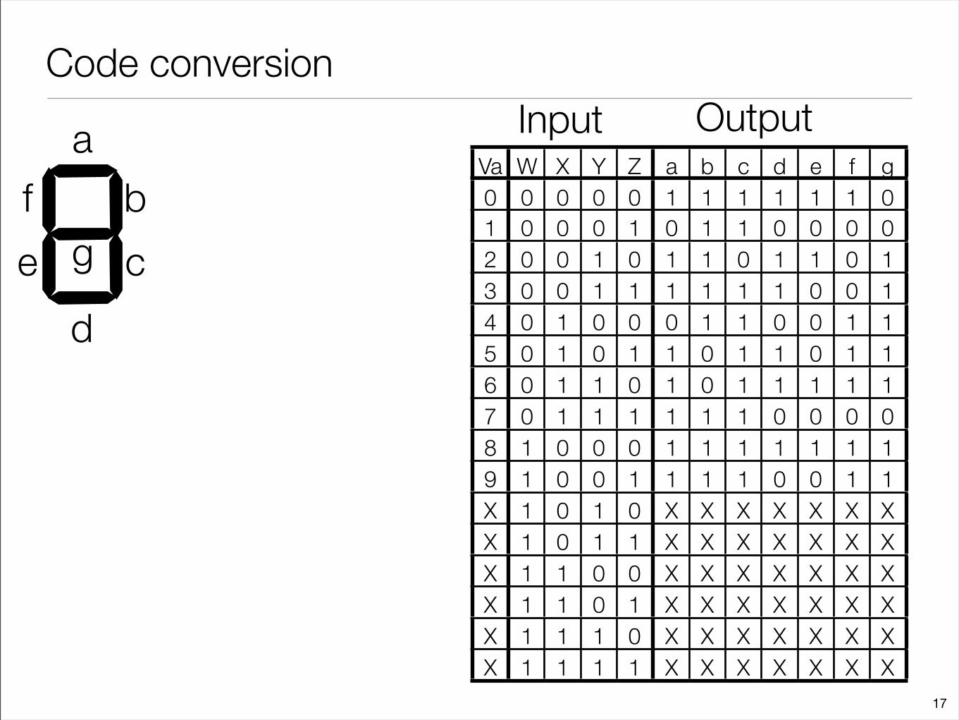
Adder/subtractor for #’s in 2’s complement form
33
© 2008 Pearson Education, Inc.M. Morris Mano & Charles R. KimeLOGIC AND COMPUTER DESIGN FUNDAMENTALS, 4e
4-7
FA FA FA FA
S
B3
C3
S2 S1 S0S3C4
C2 C1 C0
A3 B2 A2 B1 A1 B0 A0
S=0: B unchanged, C0=0: add
S=1: B complemented,
C0=1 (bits flipped and 1 added):
subtract

Handling overflow
34
0
0000
-8
1000
4
0100
-4
1100
1
0001
2
0010
3
0011
5
0101
6
0110
7
0111
-7
1001
-5
1011
-6
1010
-1
1111
-2
1110
-3
1101
0111(5) 0101(3) 0011 1000 (-8)
1111(-5) 1011(-3) 1101 1000 (-8)
1000(-6) 1010(-3) 1101 0111 (7)
0010(-6) 1010(3) 0011 1101 (-3)
twos-complement

Handling overflow
35
a3 b3 c3 c4 s3 overflow?0 0 0 0 0 0
0 0 1 0 1 1
0 1 0 0 1 0
0 1 1 1 0 0
1 0 0 0 1 0
1 0 1 1 0 0
1 1 0 1 0 1
1 1 1 1 1 0
c4 c3 c2 c1 c0 a3 a2 a1 a0 b3 b2 b1 b0 s3 s2 s1 s0
n bit two’s comp: -2^n <---> 2^n - 1split into pos and neg ranges and find smallest and largest possible results. show that they’re in range for twos comp.
sum of two pos is pos
sum of two negs is neg

Overflow computation in adder/subtractor
For 2’s complement, overflow if 2 most significant carries differ
36
FAFAC3C4
= 0 then no overflow,= 1 then overflow

Ripple-Carry adder circuit depth
• Depth of a circuit is the longest (most gates to go through) path
• Overflow has depth 8
• S3 has depth 7
• In general, Si has depth 2i+1 in Ripple-Carry Adder
37
A0B0A1B1A2B2A3B3
S0S1S3 S2
A3A2A1A0 + B3B2B1B0 = S3S2S1S0
Overflow

Carry lookahead adder (CLA)
• Goal: produce an adder of shorter circuit depth
• Start by rewriting the carry function
38
ci+1 = aibi + aici + bici
ci+1 = aibi + ci (ai+bi)ci+1 = gi + ci (pi)
carry propagatepi = ai + bi
carry generategi = aibi

Carry lookahead adder (CLA) (2)
• Can recursively define carries in terms of propagate and generate signals
• ith carry has i+1 product terms, the largest of which has i+1 literals
• If AND, OR gates can take unbounded inputs: total circuit depth is 2 (SoP form)
• If gates take 2 inputs, total circuit depth is 1 + log2 k for k-bit addition
39
c1 = g0 + c0p0
c2 = g1 + c1p1
= g1 + (g0 + c0p0)p1
= g1 + g0p1 + c0p0p1
c3 = g2 + c2p2
= g2 + (g1 + g0p1 + c0p0p1)p2
= g2 + g1p2 + g0p1p2 + c0p0p1p2

Carry lookahead adder (CLA) (3)
40
c0 = 0 s0 = a0 ⊕ b0 ⊕ c0
c1 = g0 + c0p0 s1 = a1 ⊕ b1 ⊕ c1
c2 = g1 + g0p1 + c0p0p1 s2 = a2 ⊕ b2 ⊕ c2
c3 = g2 + g1p2 + g0p1p2 + c0p0p1p2 s3 = a3 ⊕ b3 ⊕ c3
c4 = g3 + g2p3 + g1p2p3 + g0p1p2p3 + c0p0p1p2p3 s4 = a4 ⊕ b4 ⊕ c4
A2B2 A0B0A1B1
g2 p2 g1 p1 g0 p0 c0
c3
Depth of 3 for all ci
Depth of 4 for all si, i>0
Note: gates take only 2 inputs: depth increases by a log2 factor: still much less than linear of ripple-carry adder

Contraction
41
Contraction is the simplification of a circuit through constant input values.

Contraction example: adder to incrementer
42
adder
a4
b4
adder
a3
b3
adder
a2
b2
adder
a1
b1
adder
a0
b0
s0s1s2s3s4
1000
• What is the hardware and delay savings of implementing an incrementer using contraction?
Can be reduced to half-adders
Incrementer circuit
a0 S C
0 1 0
1 0 1S0=a0, C0=a0

Multi-wire notation
• Useful when running a bunch of bits in parallel to the same (similar place)
43
C1 C2
O0
O1
Ok-1Ok
I0I1
Ik-1Ik
... ... ... C1 C2k
k
k w
ires
k
k w
ires

Shifter Circuit
• Shifts bits of a word:
• Various types of shifters
• Barrel: selector bits indicate (in binary) how “far” bits shift
• selector value = j, then Bi = Ai-j
• bits can “wraparound” Bi (mod 2n) = Ai-j (mod 2n) or rollout (Bi=0 for i<j)
• L/R with enable: n=2, high bit enables, low bit indicates direction (e.g., 0=left [Bi = Ai-1], 1=right [Bi = Ai+1])
44
Shifter
Bk-1Bk-2...B2B1B0
Ak-1Ak-2...A2A1A0
n selector bits
k
k
n

Barrel Shifter Design with wraparound (using MUXs)
• Basic form of design: Each Ai feeds into each MUX connecting to Bj into input (j-i) mod 4
45
MUXMUX MUX MUX3 2 1 0 3 2 1 0 3 2 1 0 3 2 1 0
B3
A3 A2 A1 A0
B2 B1 B0
S1S0

Barrel Shifter Design with wraparound (using MUXs)
• Basic form of design: Each Ai feeds into each MUX connecting to Bj into input (j-i) mod 4
• Selector is 10 (i.e., 2 binary):
• each MUX entry 2 is selected
• A0 flows into the ‘2’ input of the MUX whose output is B2
46
MUXMUX MUX MUX3 2 1 0 3 2 1 0 3 2 1 0 3 2 1 0
B3
A3 A2 A1 A0
B2 B1 B0
102
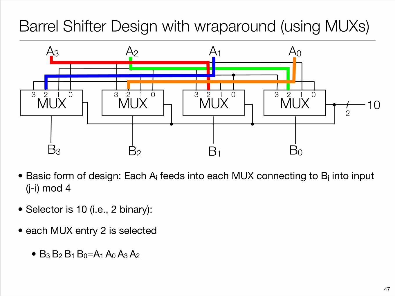
Barrel Shifter Design with wraparound (using MUXs)
• Basic form of design: Each Ai feeds into each MUX connecting to Bj into input (j-i) mod 4
• Selector is 10 (i.e., 2 binary):
• each MUX entry 2 is selected
• B3 B2 B1 B0=A1 A0 A3 A2
47
MUXMUX MUX MUX3 2 1 0 3 2 1 0 3 2 1 0 3 2 1 0
B3
A3 A2 A1 A0
B2 B1 B0
102

L/R Shift w/ Rollout
• Basic form of design:
• 0 & 1 MUX selectors (S1 = 0) feed Ai to Bi
• 2 MUX selector feeds from left (Bi = Ai-1), 3 MUX from right (Bi = Ai+1)
• Note 0 feeds (0’s roll in when bits rollout)
48
MUXMUX MUX MUX3 2 1 0 3 2 1 0 3 2 1 0 3 2 1 0
B3
A3 A2 A1 A0
B2 B1 B0
S1S0
0
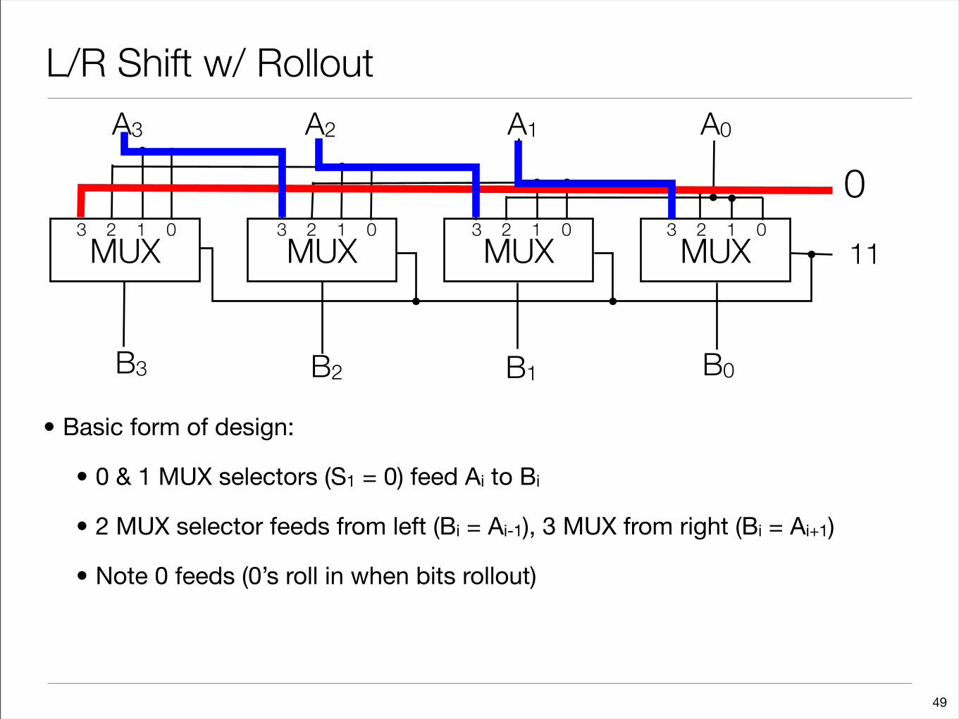
L/R Shift w/ Rollout
• Basic form of design:
• 0 & 1 MUX selectors (S1 = 0) feed Ai to Bi
• 2 MUX selector feeds from left (Bi = Ai-1), 3 MUX from right (Bi = Ai+1)
• Note 0 feeds (0’s roll in when bits rollout)
49
MUXMUX MUX MUX3 2 1 0 3 2 1 0 3 2 1 0 3 2 1 0
B3
A3 A2 A1 A0
B2 B1 B0
11
0