Embed Size (px)
DESCRIPTION
notes
Citation preview

NRI Institute of Technology
1
UNIT-4 GATE LEVEL DESIGN
Introduction
The module (integrated circuit) is implemented in terms of logic gates and interconnections between these gates. Designer should know the gate-level diagram of the design. In general, gate-level modeling is used for implementing lowest level modules in a design like, full-adder, multiplexers, etc.
Boolean algebra is used to represent logical(combinational logic) functions of digital circuits. A combinational logic expression is a mathematical formula which is to be interpreted using the laws of Boolean algebra. Now the goal of logic design or optimization is to find a network of logic gates that together compute the combinational logic function we want.
For example, given the expression a+b , we can compute its truth value for any given values of a and b , and also we can evaluate relationships such as a+b = c. but logic design is difficult for many reasons:
• We may not have a logic gate for every possible function, or even for every function of n inputs.
• Not all gate networks that compute a given function are alike-networks may differ greatly in their area and speed.
• Thus combinational logic expressions are the specification, Logic gate networks are the implementation, Area, delay, and power are the costs.
• A logic gate is an idealized or physical device implementing a Boolean function, that is, it performs a logical operation on one or more logic inputs and produces a single logic output.
• Logic gates are primarily implemented using diodes or transistors acting as electronic switches, but can also be constructed using electromagnetic relays (relay logic), fluidic logic, pneumatic logic, optics, molecules, or even mechanical elements.
• With amplification, logic gates can be cascaded in the same way that Boolean functions can be composed, allowing the construction of a physical model of all of Boolean logic.
• simplest form of electronic logic is diode logic. This allows AND and OR gates to be built, but not inverters, and so is an incomplete form of logic. Further, without some kind of amplification it is not possible to have such basic logic operations cascaded as required for more complex logic functions.
• To build a functionally complete logic system, relays, valves (vacuum tubes), or transistors can be used.
• The simplest family of logic gates using bipolar transistors is called resistor-transistor logic (RTL). Unlike diode logic gates, RTL gates can be cascaded indefinitely to produce more complex logic functions. These gates were used in early integrated circuits. For

NRI Institute of Technology
2
higher speed, the resistors used in RTL were replaced by diodes, leading to diode-transistor logic (DTL).
• Transistor-transistor logic (TTL) then supplanted DTL with the observation that one transistor could do the job of two diodes even more quickly, using only half the space.
• In virtually every type of contemporary chip implementation of digital systems, the bipolar transistors have been replaced by complementary field-effect transistors (MOSFETs) to reduce size and power consumption still further, thereby resulting in complementary metal–oxide–semiconductor (CMOS) logic. that can be described with Boolean logic.
cMOS logic gates and other complex gates
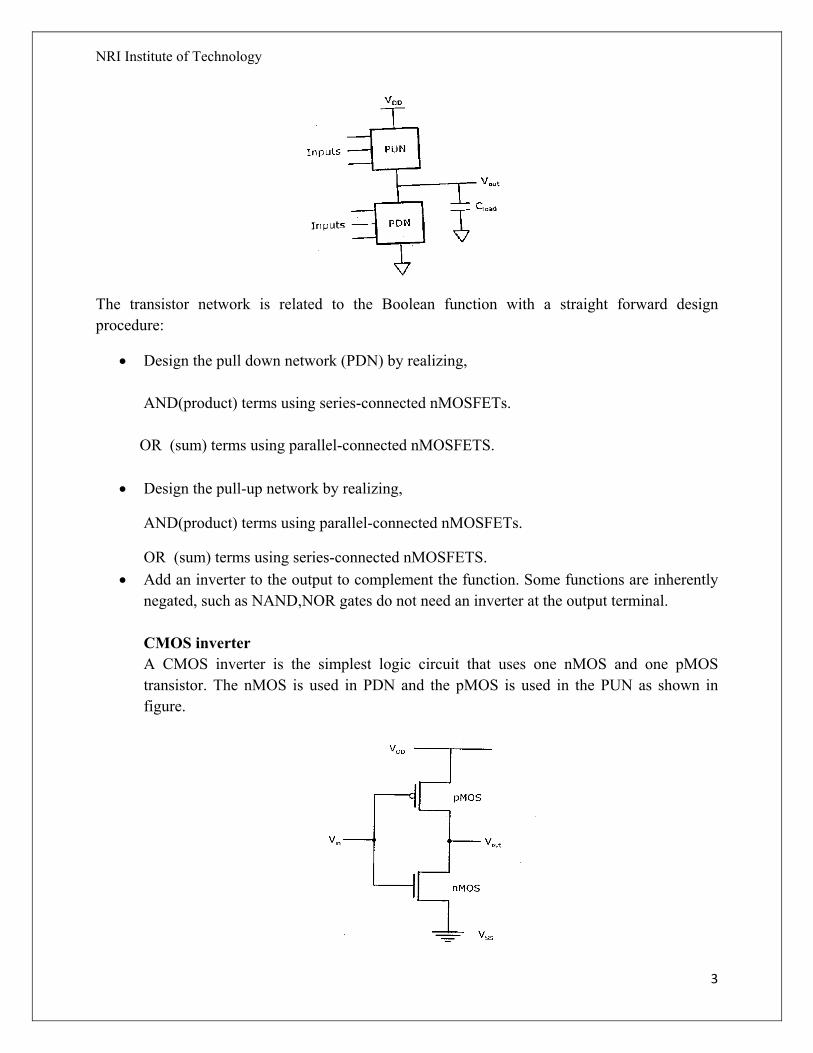
General logic circuit Any Boolean logic function (F) has two possible values, either logic 0 or logic 1. For some of the input combinations, F = 1 and for all other input combinations, F = 0. So in general, any Boolean logic function can be realized using a structure as shown in figure.
• The switch S1 is closed and switch S2 is open for input combinations that produces F = 1. • The switch S1 is open and switch S2 is closed for input combinations that produces F = 1. • The switch S1 is open and switch S2 is open for input combinations that produces F = 0.
Thus the output (F) is either connected to VDD or the ground, where the logic 0 is represented by the ground and the logic 1 is represented by VDD. So the requirement of digital logic design is to implement the pull-up switch(S1) and the pull-down switch(S2).
CMOS static logic
A generalized CMOS logic circuit consists of two transistor nets nMOS and pMOS. The pMOS transistor net is connected between the power supply and the logic gate output called as pull-up network , Whereas the nMOS transistor net is connected between the output and ground called as pull-down network. Depending on the applied input logic, the PUN connects the output node to VDD and PDN connects the output node to the ground.
NRI Institute of Technology
3
The transistor network is related to the Boolean function with a straight forward design procedure:
• Design the pull down network (PDN) by realizing,
AND(product) terms using series-connected nMOSFETs.
OR (sum) terms using parallel-connected nMOSFETS.
• Design the pull-up network by realizing,
AND(product) terms using parallel-connected nMOSFETs.
OR (sum) terms using series-connected nMOSFETS. • Add an inverter to the output to complement the function. Some functions are inherently
negated, such as NAND,NOR gates do not need an inverter at the output terminal. CMOS inverter A CMOS inverter is the simplest logic circuit that uses one nMOS and one pMOS transistor. The nMOS is used in PDN and the pMOS is used in the PUN as shown in figure.

NRI Institute of Technology
4
Working operation 1) When the input Vin is logic HIGH, then the nMOS transistor is ON and the pMOS
transistor is OFF. Thus the output Y is pulled down to ground (logic 0) since it is connected to ground but not to source VDD.
2) When the input Vin is logic LOW, then nMOS transistor is OFF and the pMOS transistor is ON, Thus the output Y is pulled up to VDD(logic 1) since it is connected to source via pMOS but not to ground.
CMOS NAND gate
The two input NAND function is expressed by Y=A.B
Step 1 Take complement of Y
Y= A.B = A.B
Step 2 Design the PDN
In this case, there is only one AND term, so there will be two nMOSFETs in series as shown in figure.
Step 3 Design the PUN. In PUN there will be two pMOSFETs in parallel , as shown in figure

NRI Institute of Technology
5
Finally join the PUN and PDN as shown in figure which realizes two –input NAND gate. Note that we have realized y, rather tat Y because the inversion is automatically provided by the nature of the CMOS circuit operation,
Working operation
1) Whenever at least one of the inputs is LOW, the corresponding pMOS transistor will conduct while the corresponding nMOS transistor will turn OFF. Subsequently, the output voltage will be HIGH.
2) Conversely, if both inputs are simultaneously HIGH, then both pMOS transistors will turn OFF, and the output voltage will be pulled LOW by the two conducting nMOS transistors.
CMOS NOR gate The two input NOR function is expressed by Y=A+B
Step 1 Take complement of Y
Y= A+B = A+B
Step 2 Design the PDN
In this case, there is only one OR term, so there will be two nMOSFETs connected in parallel, as shown in figure.
Step 3 Design the PUN
In PUN there will be two pMOSFETs in series , as shown in figure

NRI Institute of Technology
6
Finally join the PUN and PDN as shown in figure which realizes two –input NAND gate. Note that we have realized y, rather tat Y because the inversion is automatically provided by the nature of the cMOS circuit operation,
Working operation
1) Whenever at least one of the inputs is LOW, the corresponding pMOS transistor will conduct while the corresponding nMOS transistor will turn OFF. Subsequently, the output voltage will be HIGH.
2) Conversely, if both inputs are simultaneously HIGH, then both pMOS transistors will turn OFF, and the output voltage will be pulled LOW by the two conducting nMOS transistors.

NRI Institute of Technology
7
Complex gates in CMOS logic
A complex logic gate is one that implements a function that can provide the basic NOT, AND and OR operation but integrates them into a single circuit. CMOS is ideally suited for creating gates that have logic equations by exhibiting the following,
1) AND-OR-INVERT - AOI form 2) OR-AND-INVERT - OAI form
An AOI logic equation is equivalent to a complemented SOP from, while an AOI equation is equivalent to a complemented POS structure. In CMOS, output always produces NOT operation acting on input variable.
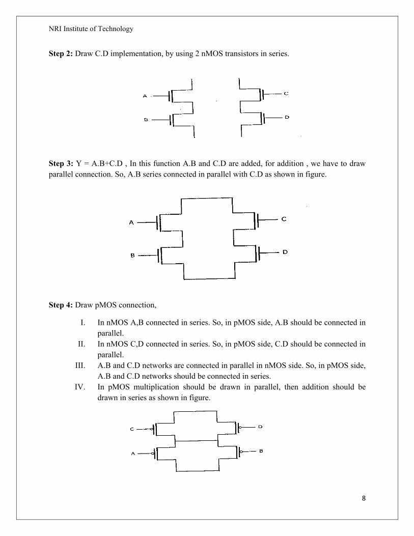
1) AOI Logic Function (OR) Design of XOR gate using CMOS logic. AND-OR-INVERT logic function(AOI) implements operation in the order AND,OR,NOT. For example , let us consider the function Y = AB+CD i.e., Y = NOT((A AND B)OR (C AND D)) The AOI logic gate implementation for Y
CMOS implementation for Y
Step 1: Draw A.B (AND) function first by connecting 2 nMOS transistors in series.
NRI Institute of Technology
8
Step 2: Draw C.D implementation, by using 2 nMOS transistors in series.
Step 3: Y = A.B+C.D , In this function A.B and C.D are added, for addition , we have to draw parallel connection. So, A.B series connected in parallel with C.D as shown in figure.
Step 4: Draw pMOS connection,
I. In nMOS A,B connected in series. So, in pMOS side, A.B should be connected in parallel.
II. In nMOS C,D connected in series. So, in pMOS side, C.D should be connected in parallel.
III. A.B and C.D networks are connected in parallel in nMOS side. So, in pMOS side, A.B and C.D networks should be connected in series.
IV. In pMOS multiplication should be drawn in parallel, then addition should be drawn in series as shown in figure.

NRI Institute of Technology
9
Step 5: Take output at the point in between nMOS and pMOS networks.
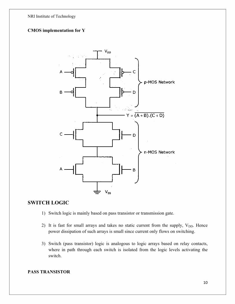
1) OAI Logic Function (OR) Design of XNOR gate using CMOS logic. OR-AND-INVERT logic function(AOI) implements operation in the order OR,AND,NOT. For example , let us consider the function Y = (A+B).(C+D) i.e., Y = NOT((A OR B)AND (C OR D)) The OAI logic gate implementation for Y
NRI Institute of Technology
10
CMOS implementation for Y
SWITCH LOGIC
1) Switch logic is mainly based on pass transistor or transmission gate.
2) It is fast for small arrays and takes no static current from the supply, VDD. Hence power dissipation of such arrays is small since current only flows on switching.
3) Switch (pass transistor) logic is analogous to logic arrays based on relay contacts,
where in path through each switch is isolated from the logic levels activating the switch.
PASS TRANSISTOR

NRI Institute of Technology
11
1) This logic uses transistors as switches to carry logic signals from node to node instead of connectiong output nodes directly to VDD or ground(GND)
2) If a single transistor is a switch between two nodes, then voltage degradation.equal to vt (threshold voltage) for high or low level depends up on nMOS or pMOS logic.
3) When using nMOS switch logic no pass transistor gate input may be driven through
one or more pass transistors as shown in figure.
4) Since the signal out of pass transistor T1 does not reach a full logic 1 by threshold voltage effects signal is degraded by below a tru e logic 1, this degraged voltage would not permit the output of T2 to reach an acceptable logic 1 level.
Advantages
They have topological simplicity.
1) Requires minimum geometry. 2) Do not dissipate standby power, since they do not have a path from supply to ground.
Disadvantages
1) Degradation in the voltage levels due to undesirable threshold voltage effects. 2) Never drive a pass transistor with the output of another pass transistor.
TRANSMISSION GATE

NRI Institute of Technology
12
1) It is an electronic element, good non-mechanical relay built with CMOS technology.
2) It is made by parallel combination of an nMOS and pMOS transistors with the input at gate of one transistor being complementary to the input at the gate of the other as shown in figure.
3) Thus current can flow through this element in either direction.
4) Depending on whether or not there is a voltage on the gate, the connection between the input and output is either low resistance or high-resistance, respectively Ron = 100Ω and Roff > 5 MΩ.
Operation
• When the gate input to the nMOS transistor is ‘0’ and the complementary ‘1’ is gate input to the pMOS , thus both are turned off.
• When gate input to the nMOS is ‘1’ and its complementary ‘0’ is the gate input to the pMOS , both are turned on and passes any signal ‘1’ and ‘0’ equally without any degradation.
• The use of transmission gates eliminates the undesirable threshold voltage effects which give rise to loss of logic levels in pass-transistors as shown in figure.
Advantages
1) Transmission gates eliminates the signal degradation in the output logic levels. 2) Transmission gate consists of two transistors in parallel and except near the positive and
negative rails.
Disadvantages
1) Transmission gate requires more area than nMOS pass circuitry. 2) Transmission gate requires complemented control signals.
“ Transmission gate logic can be used to design multiplexers(selector functions)”.
NRI Institute of Technology
13
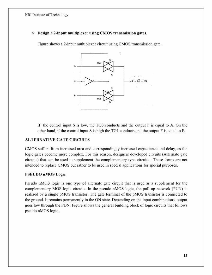
Design a 2-input multiplexer using CMOS transmission gates.
Figure shows a 2-input multiplexer circuit using CMOS transmission gate.
If the control input S is low, the TG0 conducts and the output F is equal to A. On the other hand, if the control input S is high the TG1 conducts and the output F is equal to B.
ALTERNATIVE GATE CIRCUITS
CMOS suffers from increased area and correspondingly increased capacitance and delay, as the logic gates become more complex. For this reason, designers developed circuits (Alternate gate circuits) that can be used to supplement the complementary type circuits . These forms are not intended to replace CMOS but rather to be used in special applications for special purposes.
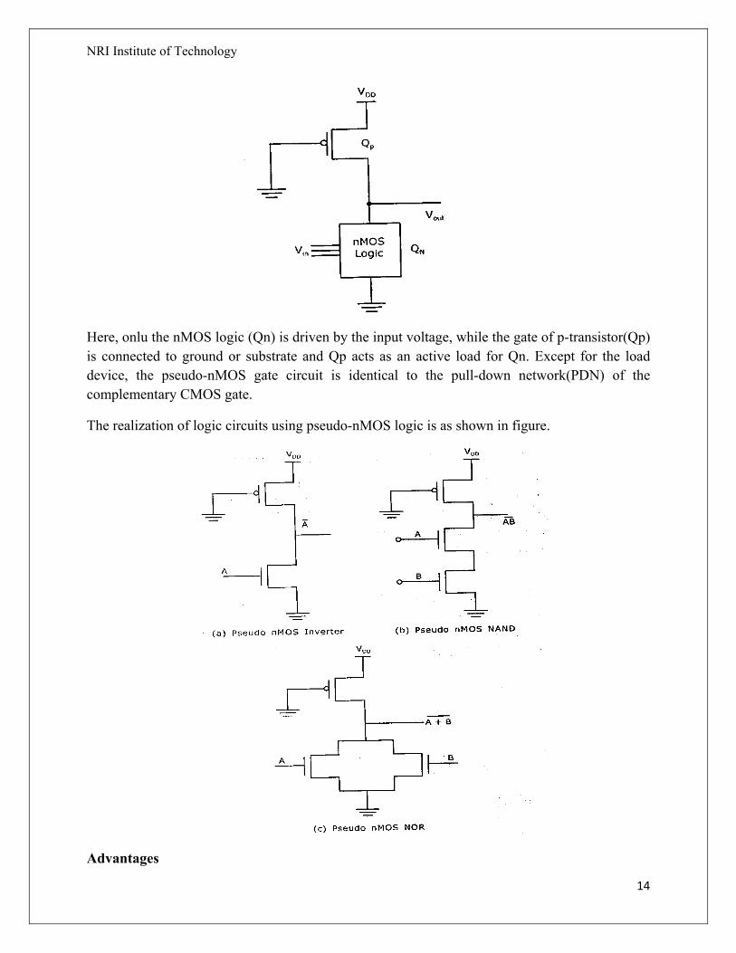
PSEUDO nMOS Logic
Pseudo nMOS logic is one type of alternate gate circuit that is used as a supplement for the complementary MOS logic circuits. In the pseudo-nMOS logic, the pull up network (PUN) is realized by a single pMOS transistor. The gate terminal of the pMOS transistor is connected to the ground. It remains permanently in the ON state. Depending on the input combinations, output goes low through the PDN. Figure shows the general building block of logic circuits that follows pseudo nMOS logic.
NRI Institute of Technology
14
Here, onlu the nMOS logic (Qn) is driven by the input voltage, while the gate of p-transistor(Qp) is connected to ground or substrate and Qp acts as an active load for Qn. Except for the load device, the pseudo-nMOS gate circuit is identical to the pull-down network(PDN) of the complementary CMOS gate.
The realization of logic circuits using pseudo-nMOS logic is as shown in figure.
Advantages

NRI Institute of Technology
15
1) Uses less number of transistors as compared to CMOS logic.
2) Geometrical area and delay gets reduced as it requires less transistors.
3) Low power dissipation.
Disadvantages
1) The main drawback of using a pseudo nMOS gate instead of a CMOS gate is that the always on PMOS load conducts a steady current when the output voltage is lower than VDD.
2) Layout problems are critical.
DYNAMIC CMOS LOGIC
A dynamic CMOS logic uses charge storage and clocking properties of MOS transistors to implement logic operations. Figure shows the basic building block of dynamic CMOS logic. Here the clock ø drives nMOS evaluation transistor and pMOS precharge transistor. A logic is implemented using an nFET array connected between output node and ground.
The gate (clock ø) defines two phases, evaluation and precharge phase during each clock cycle.
Working

NRI Institute of Technology
16
• When clock ø = 0 the circuit is in precharge phase with the pMOS device Mp ON and the evaluation nMOS Mn OFF. This establishes a conducting path between VDD and the output allowing Cout to charge to a voltage Vout = VDD. Mp is often called the precharge FET.
• When clock ø = 1 the circuit is in evaluation phase with the pMOS device Mp OFF and the evaluation nMOS Mn ON. If the logic block acts like a closed switch the Cout can discharge through logic array and Mn, this gives a final result of Vout = VDD, logically this is an output of F = 1. Charge leakage eventually drops the output to Vout = 0 Vwhich could be an incorrect logic value.
The logic formation is formed by three series connected FETs (3-input NAND gate) is shown in figure.
The dynamic CMOS logic circuit has a serious problem when they are cascaded. In the precharged phase (ø = 0) , output of all the stages are pre-charged to logic high. In the evaluation phase (ø = 1), the output of all stages are evaluated simultaneously. Suppose in the first stage, the inputs are such that the output is logic low after the evaluation. In the second stage, the output of the first stage is one input and there are other inputs. If theouther inputs of the second stage are such that output of it discharges to logic low, then the evaluated output of the first stage can never make the output of the second stage logic high. Ths is because, by the time the first stage is being evaluated, output of the second. Stage is discharged, since evaluation happens simultaneously. Remember that the output cannot be charged to logic high in the evaluation phase (ø = 1, pMOSFET in PUN is OFF), it can only be retained in the logic high depending on the inputs.

NRI Institute of Technology
17
Advantages
1) Low power dissipation.
2) Large noise margin.
3) Small area due to less number of transistors.\
CMOS DOMINO LOGIC
Standard CMOS logic gates need a PMOS and an NMOS transistor for each logic input. The pMOS transistors require a greater area tan the nMOS transistors carrying the same current. So, a large chip area is necessary to perform complex logic operations. The package density in CMOS is improved if a dynamic logic circuit, called the domino CMOS logic circuit, is used.
Domino CMOS logic is slightly modified version of the dynamic CMOS logic circuit. In this case, a static inverter is connected at the output of each dynamic CMOS logic block. The addition of the inverter solves the problem of cascading of dynamic CMOS logic circuits.
The circuit diagram of domino CMOS logic structures as shown in figure as follows
A domino CMOS AND-OR gate that realizes the function y = AB + CD is depicted in fugure . The left hand part of the circuit containing Mn,Mp, T1,T2,,T3,and T4 forms and AND-OR-INVERTER (AOI) gate. It derives the static CMOS inverter formed by N2 and P2 in the right-

NRI Institute of Technology
18
hand part of the circuit. The domino gate is activated by the single phase clock ø applied to the NMOS (Mn) and the PMOS (Mp) transistors. The load on the AOI part of the circuits is the parasitic load capacitance.
Working
• When ø = 0, is ON and Mn is OFF, so that no current flows in the AND-OR paths of the AOI. The capacitor CL is charged to VDD through Mp since the latter is ON. The input to the inverter is high, and drives the output voltage V0 to logic-0.
• When ø = 1, Mp is turned OFF and Mn is turned ON. If either (or both) A and B or C and D is at logic-1, CL discharges through either T2,T1 and Mn or T3,T4 and Mp. So , the inverter input is driven to logic-0 and hence the output voltage V0 to logic-1. The Boolean expression for the output voltage is Y = AB + CD.
Note : Logic input can change only when ø = 0. No changes of the inputs are permitted when ø = 1 since a discharge path may occur.
Advantages
1) Smaller areas compared to conventional CMOS logic.
2) Parasitic capacitances are smaller so that higher operating speeds are possible.
3) Operation is free of glitches since each gate can make one transition.
disadvantages
1) Non inverting structures are possible because of the presence of inverting buffer.
2) Charge distribution may be a problem.
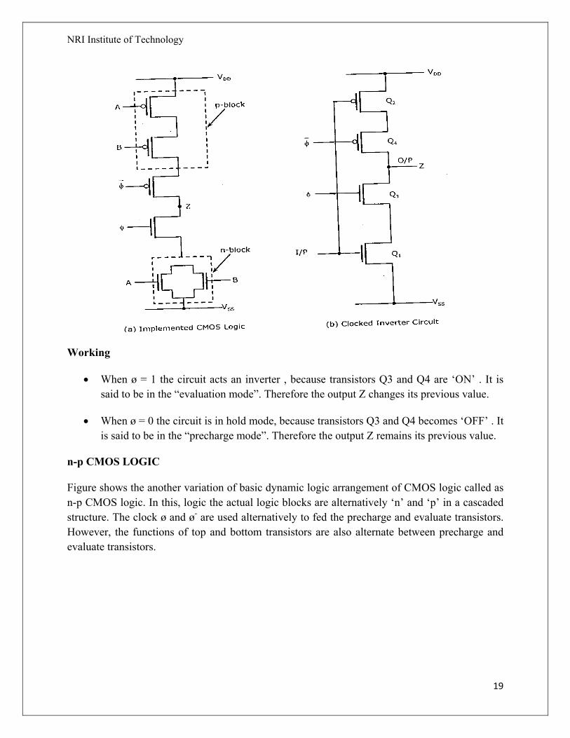
CLOCKED CMOS LOGIC
The clocked CMOS logic is also referred as C2MOS logic. Figure shows the general arrangement of a clocked CMOS (C2MOS) logic. A pull-up p-block and a complementary n-block pull-down structure represent p and n-transistors respectively and are used as implement clocked CMOS logic shown in figure. However, the logic in this case is connected to the output only during the ON period of the clock. Figure shows a clocked inverter circuit which is also belongs to clocked CMOS logic family. The slower rise times and fall times can be expected due to owing of extra transistors in series with the output.
NRI Institute of Technology
19
Working
• When ø = 1 the circuit acts an inverter , because transistors Q3 and Q4 are ‘ON’ . It is said to be in the “evaluation mode”. Therefore the output Z changes its previous value.
• When ø = 0 the circuit is in hold mode, because transistors Q3 and Q4 becomes ‘OFF’ . It is said to be in the “precharge mode”. Therefore the output Z remains its previous value.
n-p CMOS LOGIC
Figure shows the another variation of basic dynamic logic arrangement of CMOS logic called as n-p CMOS logic. In this, logic the actual logic blocks are alternatively ‘n’ and ‘p’ in a cascaded structure. The clock ø and ø- are used alternatively to fed the precharge and evaluate transistors. However, the functions of top and bottom transistors are also alternate between precharge and evaluate transistors.

NRI Institute of Technology
20
Working
• During the pre charge phase ø = 0 , the output of the n-tree gate, OUT 1 OUT3 , are charged to VDD, while the output of the p-tree gate OUT2 is pre discharged to 0V. Since the n-tree gate connects pMOS pull-up devices, the PUN of the p-tree is turned off at that time.
• During the evaluation phase ø = 1, the outputs (OUT1,OUT3) of the n-tree gate can only make a 1- 0 transition, conditionally turning on some transistors in the p-tree. This ensures that no accidental discharge of OUT 2 can occur.
• Similarly n-tree blocks can follow p-tree gates without any problems, because the inputs to the n-gate are pre charged to 0.
Disadvantages
Here, the p-tree blocks are slower than the n-tree modules, due to the lower current drive of the pMOS transistors in the logic network.
NRI Institute of Technology
21
BASIC CIRCUIT CONCEPTS
In VLSI design the wiring up (interconnection) of circuits takes place through the various conductive layers which are produced by the MOS processing. So, it is necessary to know the resistive and capacitive characteristics of each layer. Concepts such as
• resistance RS and a standard unit of capacitance cg which helps in evaluating the effects of wiring and input and output capacitances.
• The delays associated with wiring with inverters and with other circuitry evaluated interms of a delay unit τ.
Sheet Resistance RS
• The sheet resistance is a measure of resistance of thin films that have a uniform thickness. • It is commonly used to characterize materials made by semiconductor doping, metal
deposition, resistive paste printing and glass coating. Ex: doped semiconductor regions (silicon or polysilicon ) and resistors.
• Sheet resistance is applicable to two-dimensional systems where the thin film is considered to be a two- dimensional entity.
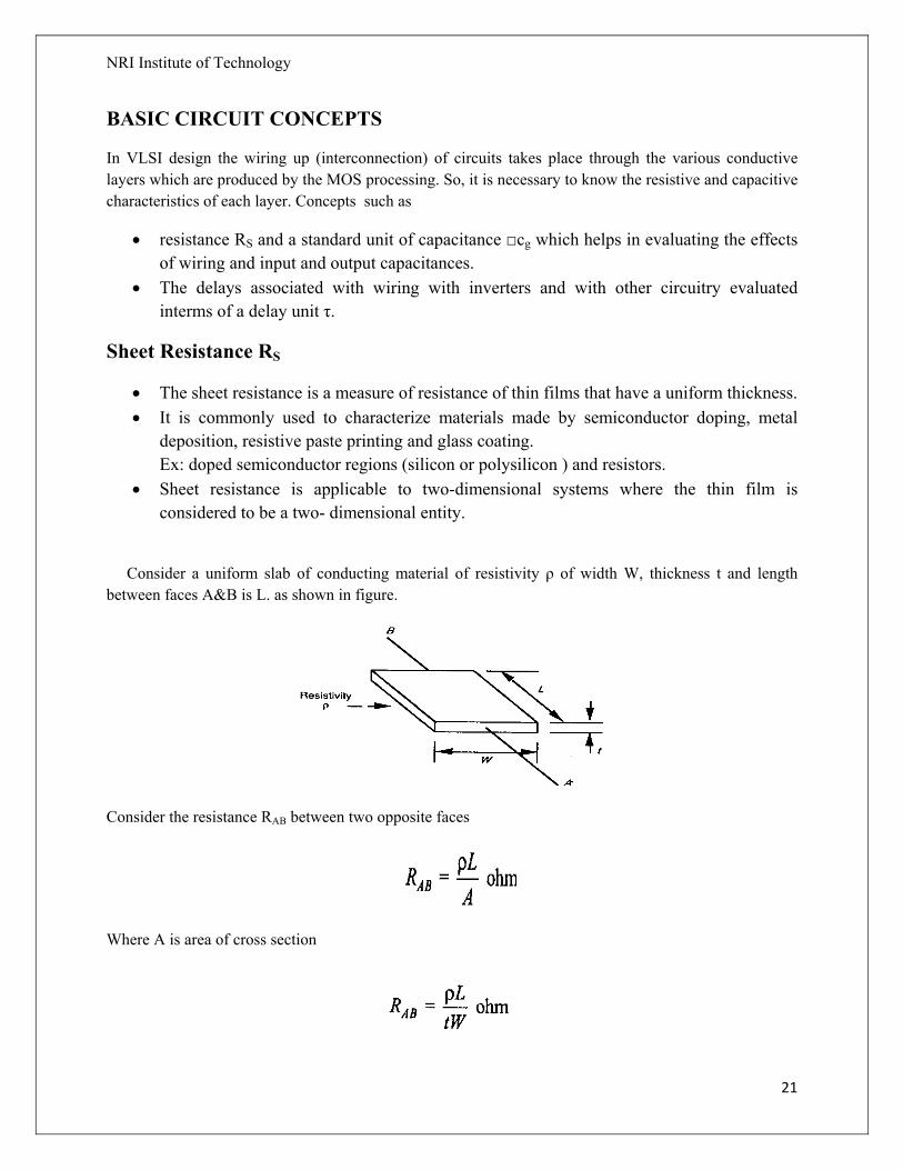
Consider a uniform slab of conducting material of resistivity ρ of width W, thickness t and length between faces A&B is L. as shown in figure.
Consider the resistance RAB between two opposite faces
Where A is area of cross section

NRI Institute of Technology
22
Consider a case in which L = W . It means square of resistive material
Where RS is ohm per square or sheet resistance.
From the above equation RS is independent of the area of square., for example a 1µm per side square slab of the material has same resistance as 1 cm per side square slab of the same material if the thickness is same.
Hence, the resistance of the MOS layers depend on the thickness and the resistivity of the material of the layer.
• The thickness of the metal and polysilicon deposited is known by measuring using four probe method.
• The resistivity of the diffusion layers is measured by measuring the penetration depth of the diffusion regions.
Sheet resistance concept applied to MOS Transistors and Inverterts:
Consider the transistor structures by distinguish the actual diffusion (active) regions from the channel regions. The simple n-type pass transistor has a channel length L = 2λ and a channel width W=2λ.
Hence the channel is square and the channel resistance is

NRI Institute of Technology
23
Here the length to width ratio denotes the impedance (Z) and is equal to 1:1. Consider another transistor has a channel length L = 8λ and width W = 2λ.
Thus, channel resistance
Typical sheet resistances of MOS layers are tabulated
RS ohm per square Layer
5µm Orbit Orbit 1.2µm
Metal 0.03 0.04 0.04
Diffusion 15 - 100 20 - 45 20 - 45
Silicide 2 - 4 --- ---
Polysilicon 15 - 100 15 - 30 15 - 30
n- channel 104 2 X 10⁴ 2 X 10⁴
p-channel 2.5 X 10⁴ 4.5 X 10⁴ 4.5 X 10⁴
Sheet resistance for Inverters
Consider an nMOS inverter has the channel length 8λ and width 2λ for pull up transistor as shown in figure.
L = 8λ; W = 2λ
Z = L/W = 4

NRI Institute of Technology
24
Sheet resistance R = Z.RS = 4 X 104 = 40 KΩ
For pull down transistor the channel length 2λ and width 2λ, then the sheet resistance is
R = Z.RS = 1 X 104 = 10 KΩ
Hence Zp.u to Zp.d = 4:1 hence the ON resistance between VDD and VSS is the
total series resistance i.e.,
RON = 40 KΩ + 10 KΩ = 50 KΩ
Consider the simple CMOS inverter as shown in figure.
Here the pull up transistor is of p-type device with channel length 2λ and width 2λ.
Z = L/W =1
Then Sheet resistance RSP = Z.RS = 1 X 2.5 X 104 = 25 KΩ
The pull down transistor is of n-type with channel length 2λ and width 2λ.
Z = L/W =1
Hence, Sheet resistance RSN = Z.RS = 1 X 104 = 10 KΩ.
In this case, there is no static resistance between VDD and VSS . Since at any point of time only one transistor is ON, but not both.
When Vin = 1, the ON resistance is 10KΩ
Vin = 0, the ON resistance is 25KΩ

NRI Institute of Technology
25
Area capacitance of layers
From the concept of the transistors, it is apparent that as gate is separated from the channel by gate oxide an insulating layer, it has capacitance. Similarly different interconnects run on the chip and each layer is separated by silicon dioxide .
For any layer by knowing the dielectric thickness, we can calculate the area capacitance as follows
Where, A is area of the plates , D is the thickness of Sio2, Є0 is the permittivity of the free space and Єins is the relative permittivity of insulator(Sio2).
Typical area capacitance values of MOS circuits
Value in pF X 10-4/ µm2 (Relative values in brackets ) Layer
5µm Orbit Orbit 1.2µm
Gate to channel 4 (1.0) 8 (1.0) 16 (1.0)
Diffusion 1 (0.25) 1.75 (0.22) 3.75 (0.23)
Polysilicon to substrate 0.4 (0.1) 0.6 (0.075) 0.6 (0.038)
Metal 1 to substrate 0.3 (0.075) 0.33 (0.04) 0.33 (0.02)
Metal 2 to substrate 0.2 (0.05) 0.17 (0.02) 0.17 (0.01)
Metal 2 to metal 1 0.4 (0.1) 0.5 (0.06) 0.5 (0.03)
Metal 1 to poly silicon 0.3(0.075) 0.3 (0.038) 0.3 (0.018)
Standard unit of capacitance cg
It is defined as the gate – to – channel capacitance of a MOS transistor having W = L . i.e., standard square as shown in figure. The unit is denoted by cg. cg may be calculated for any MOS process as follows
For 5µm MOS circuits
Area/standard square = 5µm X 5µm = 25 µm2
Capacitance value = 4 X 10⁻⁴ pF/ µm2

NRI Institute of Technology
26
Thus, standard value cg = 25 µm2 X 4 X 10-4 pF/ µm2 = 0.01 pF
For 2µm MOS circuits
Area/standard square = 2µm X 2µm = 4 µm2
Capacitance value = 8 X 10⁻⁴ pF/ µm2
Thus, standard value cg = 4 µm2 X 8 X 10-4 pF/ µm2 = 0.01 pF
For 1.2µm MOS circuits
Area/standard square = 1.2µm X 1.2µm = 1.44 µm2
Capacitance value = 16 X 10-4 pF/ µm2
Thus, standard value cg = 1.44 µm2 X 16 X 10-4 pF/ µm2 = 0.0023 pF
Calculation for capacitance value
The calculation of capacitance value is established by the ration between the area of interest and the area
of standard gate and multiplying this ration by the appropriate relative C value from tabular form. The
product will give the required capacitance in cg units.
Consider the area defined as shown in figure of length 20λ and width 3λ
Area relative to the standard gate
Relative area = Area( L X W )/standard gate area
= 15 .

NRI Institute of Technology
27
1) consider the area in metal 1
capacitance to substrate = relative area X relative C value (from table)
= 15 X 0.075 cg
= 1.125 cg
2) consider the same area in polysilicon
capacitance to substrate = 15 X 0.1cg
= 1.5 cg
3) consider the same area in n- type diffusion
capacitance to substrate = 15 X 0.25cg
= 3.75 cg
Consider the following structure which occupies more than one layer as shown in figure and calculate the
area capacitance value
While calculating the area value in the above figure neglect the contact region where the metal is
connected to polysilicon and shielded from the substrate.

NRI Institute of Technology
28
( i)consider the metal area
Relative area = Area( L X W )/standard gate area
= 75
metal capacitance = relative area X relative C value (from table)
= 75 X 0.075 cg
= 5.625 cg
3) consider the polysilicon area (excluding the gate region)
capacitance to substrate = 15 0.1cg
= 1.5 cg
3) consider the same area in n- type diffusion
capacitance to substrate = 15 X 0.25cg
= 3.75
We know that the transit time (τsd) from source to drain
Here the Vds varies as Cg charges from 0 volts to 63% of Vdd in period τ. Thus the average value of Vds =
3V.

NRI Institute of Technology
29
For 5µm technology
τsd = 0.13 n sec, τsd τ
Similarly the transition point of an inverter or gate is 0.5 VDD which is approximately equal to 0.63 VDD
(time constant). From this we can conclude that we can use the transit time and time constant
interchangeably and ‘stray’ capacitances are allowed for doubling the theoretical values calculated.
Thus, τ is used as the fundamental time unit and all timings in a system can be assessed in relation to τ
,Hence for 5µm MOS technology τ = 0.3 nsec.
for 2µm MOS technology τ = 0.2 nsec.
for 1.2µm MOS technology τ = 0.1 nsec.
INVERTER DELAYS
Consider the basic nMOS inverter has the channel length 8λ and width 2λ for pull-up transistor and
channel length of 2λ and width 2λ for pull down transistor.
Hence the sheet resistance for pull-up transistor is Rp.u = 4RS = 40kΩ and
sheet resistance for pull-up transistor is Rp.d = 1RS = 10kΩ.
Since (τ = RC) depends upon the values of R & C, the delay associates with the inverter depend up on
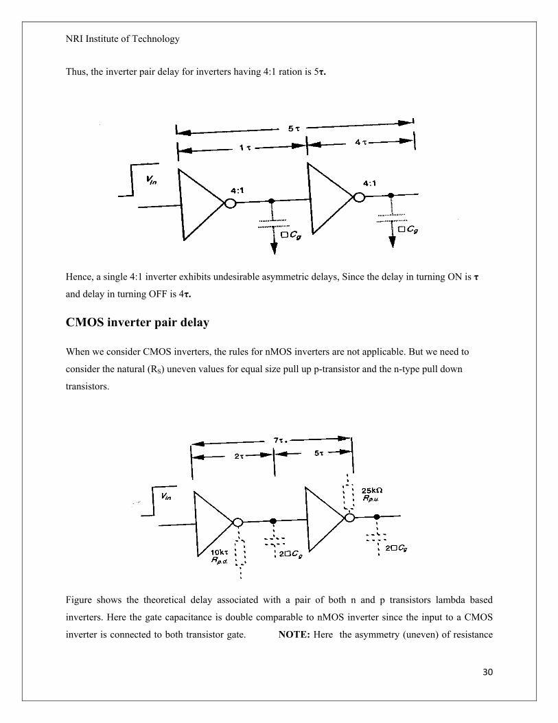
whether it is being turned on (or ) off. Now, consider a pair of cascaded inverters as shown in figure, then
the delay over the pair will be constant irrespective of the sense of the logic level transition of the input to
the first .
In general, the delay through a pair of similar nMOS inverters is Td = (1 + Zp.u/Zp.d ) τ
Assume that τ = 0.3 n sec.
Then ,Td = (1 + 4) 0.3
= 5 τ
NRI Institute of Technology
30
Thus, the inverter pair delay for inverters having 4:1 ration is 5τ.
Hence, a single 4:1 inverter exhibits undesirable asymmetric delays, Since the delay in turning ON is τ
and delay in turning OFF is 4τ.
CMOS inverter pair delay
When we consider CMOS inverters, the rules for nMOS inverters are not applicable. But we need to
consider the natural (RS) uneven values for equal size pull up p-transistor and the n-type pull down
transistors.
Figure shows the theoretical delay associated with a pair of both n and p transistors lambda based
inverters. Here the gate capacitance is double comparable to nMOS inverter since the input to a CMOS
inverter is connected to both transistor gate. NOTE: Here the asymmetry (uneven) of resistance

NRI Institute of Technology
31
values can be eliminated by increasing the width of the p-device channel by a factor of two or three at the
same time the gate capacitance of p-transistor also increased by the same factor.
Formal estimation of CMOS inverter delay
In CMOS inverter by the charging and discharging of a capacitive load CL , we can estimate the Rise
time and fall time from the following simple analysis.
Rise time estimation
In this analysis we assume that the p-device stays in saturation for the entire charging period of the load
capacitor CL.
Consider the circuit as follows
Saturation current for the p-transistor is given by
This current charges CL and since its magnitude is approximately constant, we have
Substitute the value of Idsp in above equation and then the rise time is
NRI Institute of Technology
32
Assume that t = τr when Vout = VDD then
If Vtp = 0.2VDD, then
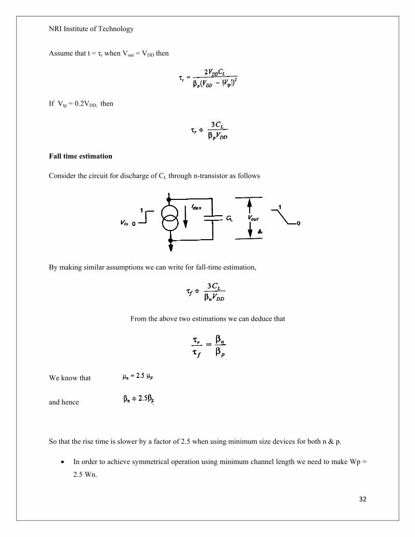
Fall time estimation
Consider the circuit for discharge of CL through n-transistor as follows
By making similar assumptions we can write for fall-time estimation,
From the above two estimations we can deduce that
We know that
and hence
So that the rise time is slower by a factor of 2.5 when using minimum size devices for both n & p.
• In order to achieve symmetrical operation using minimum channel length we need to make Wp =
2.5 Wn.

NRI Institute of Technology
33
• For minimum size lambda based geometries this would result in the inverter having an input
capacitance of
1cg (n-device) + 2.5cg(p-device) = 3.5cg
From the above equations we can conclude that
1. τr and τf are proportional to 1/VDD
2. τr and τf are proportional to CL
3. τr = 2.5τf for equal n and p- transistor geometries.
Driving Large capacitive loads
when signals are propagated from the chip to off chip destinations we can face problems to drive large
capacitive loads. Generally off chip capacitances may be several orders higher than on chip cg values.
CL ≥ 104 cg
Where CL denotes offchip load. The capacitances which of this order must be driven through low
resistances, otherwise excessively long delays will occur. Large capacitance is presented at the input,
which in turn slows down the rate of change of voltage at input.
Cascaded Inverters as drivers
Inverters to drive large capacitive loads must be present low pull-up and pull down resistance. For MOS
circuits low resistance values imply low L:W ratio(since ) . Since length L cannot be reduced
below the minimum feature size, the channels must be made very wide to reduce resistance value.
Consider N cascaded inverters as on increasing the width factor of ‘f’ than the previous stage as shown in
figure.
As the width factor increases, the capacitive load presented at the inverter input increases and the area
occupied increases also. It is observed that as the width increases, the number N of stages are decreased to
drive a particular value of CL. Thus with large f(width), N decreases but delay per stage increases for 4:1
nMOS inverters.

NRI Institute of Technology
34
Delay per stage = fτ for ∆Vin
=4fτ for ∆-Vin
Where ∆Vin indicates logic 0 to 1 transition and
∆-Vin indicates logic 1 to 0 transition of Vin
Toal delay per nMOS pair = 4fτ
Similarly delay per CMOS pair = 7fτ.
Calculation for time delay
Let us assume y = CL/cg = f N
Determine the value of f which will minimize the overall delay for a given value of y.
Apply logarithms on both sides in the above equation
ln(y) = ln(f N)
ln (y) = N ln (f)
N= ln(y)/ln(f)
For N even
Total delay = N/2 5fτ
= 2.5 Nfτ (nMOS)
(Or) toal delay = N/2 7fτ
= 3.5Nfτ (CMOS)
From above relations, we can write
Delay α Nfτ
= ln(y)/ln(f) . fτ
NRI Institute of Technology
35
It can be shown that total delay is minimized if f assumes the value of e for both CMOS and
nMOS inverters.
Assume f = e N = ln(y)/ln(e)
N = ln(y)
Overall delay td N even td = 2.5 eNτ (nMOS)
(or) td = 3.5 eNτ(CMOS)
N odd td = [2.5(N-1) +1] eτ (nMOS)
td = [3.5(N-1) +2] eτ (CMOS) ( for logical transition 0 to 1)
( or) td = [ 2.5(N-1) + 4] eτ (nMOS)
td = [3.5(N-1) +5] eτ (CMOS) (for logical transition 1 to 0)
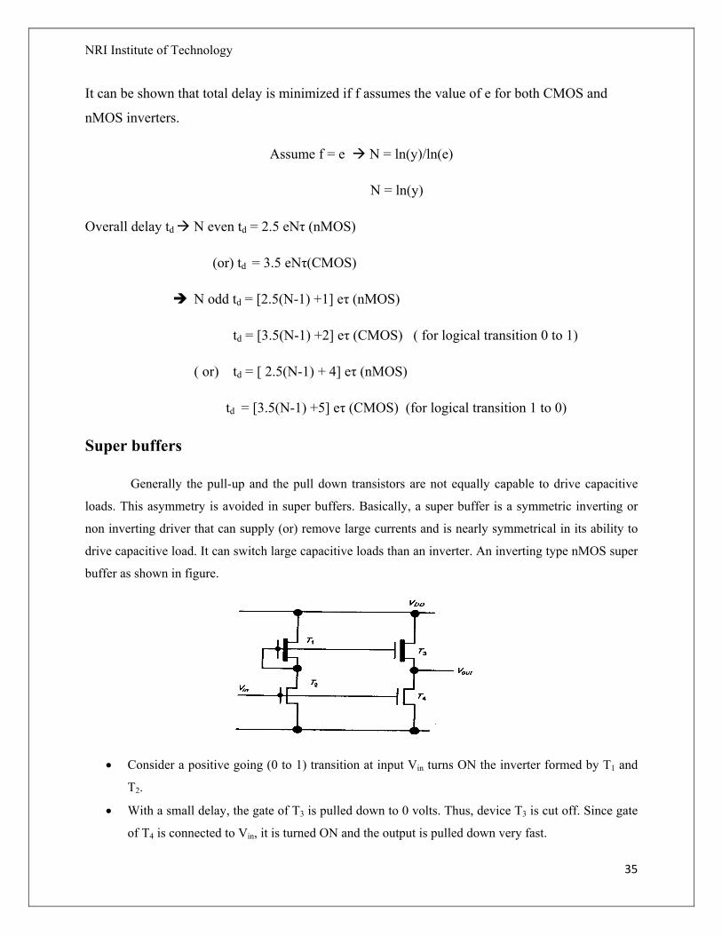
Super buffers
Generally the pull-up and the pull down transistors are not equally capable to drive capacitive
loads. This asymmetry is avoided in super buffers. Basically, a super buffer is a symmetric inverting or
non inverting driver that can supply (or) remove large currents and is nearly symmetrical in its ability to
drive capacitive load. It can switch large capacitive loads than an inverter. An inverting type nMOS super
buffer as shown in figure.
• Consider a positive going (0 to 1) transition at input Vin turns ON the inverter formed by T1 and
T2.
• With a small delay, the gate of T3 is pulled down to 0 volts. Thus, device T3 is cut off. Since gate
of T4 is connected to Vin, it is turned ON and the output is pulled down very fast.
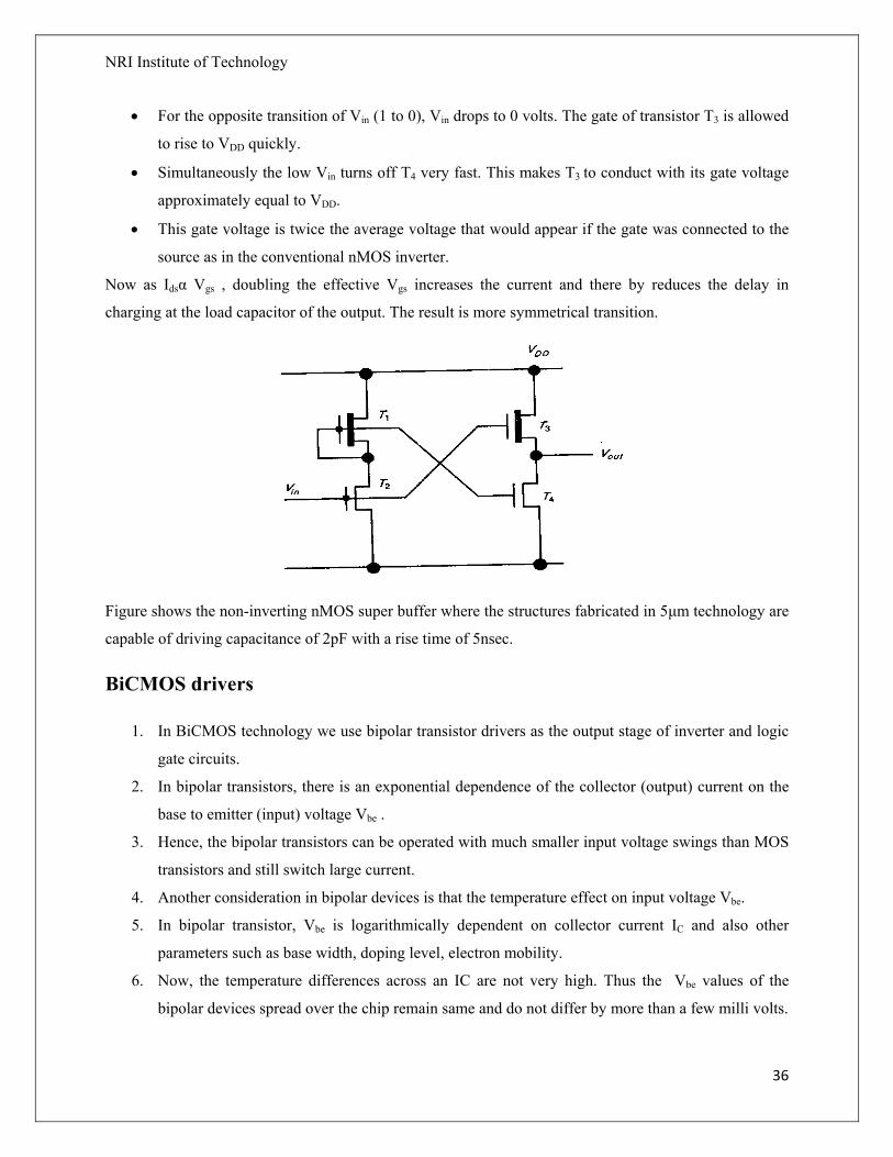
NRI Institute of Technology
36
• For the opposite transition of Vin (1 to 0), Vin drops to 0 volts. The gate of transistor T3 is allowed
to rise to VDD quickly.
• Simultaneously the low Vin turns off T4 very fast. This makes T3 to conduct with its gate voltage
approximately equal to VDD.
• This gate voltage is twice the average voltage that would appear if the gate was connected to the
source as in the conventional nMOS inverter.
Now as Idsα Vgs , doubling the effective Vgs increases the current and there by reduces the delay in
charging at the load capacitor of the output. The result is more symmetrical transition.
Figure shows the non-inverting nMOS super buffer where the structures fabricated in 5µm technology are
capable of driving capacitance of 2pF with a rise time of 5nsec.
BiCMOS drivers
1. In BiCMOS technology we use bipolar transistor drivers as the output stage of inverter and logic
gate circuits.
2. In bipolar transistors, there is an exponential dependence of the collector (output) current on the
base to emitter (input) voltage Vbe .
3. Hence, the bipolar transistors can be operated with much smaller input voltage swings than MOS
transistors and still switch large current.
4. Another consideration in bipolar devices is that the temperature effect on input voltage Vbe.
5. In bipolar transistor, Vbe is logarithmically dependent on collector current IC and also other
parameters such as base width, doping level, electron mobility.
6. Now, the temperature differences across an IC are not very high. Thus the Vbe values of the
bipolar devices spread over the chip remain same and do not differ by more than a few milli volts.

NRI Institute of Technology
37
The switching performance of a bipolar transistor driving a capacitive load can be analyzed to begin with
the help of equivalent circuit as shown in figure.
The time ∆t required to change the output voltage Vout by an amount equal to the input voltage is
∆t = CL/gm
Where,
CL is the load capacitance
gm is the trans conductance of the bipolar transistor.
The value of ∆t is small because the trans conductance of the bipolar transistors is relatively high.
There are two main components which reveals the delay due to the bipolar transistors are Tin and TL .
• Tin is the time required to first charge the base emitter junction of the bipolar (npn) transistor.
This time is typically 2ns for the BiCMOS transistor base driver.
• For the CMOS driver the time required to charge the input gate capacitance is 1ns.
• TL is the time required to charge the output load capacitance .
• The combined effect of Tin and TL is represented as shown in figure.
• Delay of BiCMOS inverter can be described by
• Delay for BiCMOS inverter s reduced by a factor of hfe as compared with a CMOS inverter.

NRI Institute of Technology
38
• In Bipolar transistors while considering delay another significant parameter is collector resistance
Rc through which the charging current for CL flows.
• For a high value of RC, there is a long propagation delay through the transistor when charging a
capacitive load.
• Figure shows the typical delay values at two values of CL as follows.
The devices thus have high β, high gm, high hfe and low RC. The presence of such efficient and
advantageous devices on chip offers a great deal of scope and freedom to the VLSI designer.
Propagation delays
Propagation delay is the delay in the propagation of the signal created by the change of logical status at
the input to create same change at the output.
(i)Cascaded pass transistors
Figure shows a chain of four pass transistors driving a capacitive load CL. All the gates are supplied by
VDD so that a signal can propagate to the output. The lamped RC equivalent circuit is shown in figure,
where each transistor is modeled by a series resistance and capacitance representing the gate-to-channel
capacitance and stray capacitances. Them minimum value of R is the turned ON resistance of each
enhancement mode pass transistor.
NRI Institute of Technology
39
The current through the capacitance at the node with voltage V2 is
C (dV2 / dt ) ≈ C.∆V2/ ∆t
The current entering at this node is I1 = (V1 – V2)/R and
the current leaving from this node is I2 = (V2 – V3)/R.
By applying KCL at this node
IC = I1 – I2
C . ∆V2/ ∆t = I1 – I2 = ((V1 – V2)- (V2 – V3)) / R
As the number of sections in the network increases, the circuit parameters become distributed.
Assume that R and C as the resistance per unit length and the capacitance per unit length respectively.
C∆* .∆V2/ ∆t = ∆(∆V2)/R.∆X
Where x is the distance along the network from the input.
RC dv/dt = d/dx. (dv/dx) = d2V/dx2
The propagation time τp from a signal to propagate a distance x is
τp α X2
By simplifying the analysis if all sheet resistance, gate-to-channel capacitance RS and cg are
lumped together
R total = nr Rs
C total = nccg
Where r gives relative resistance per section interms of RS and c gives relative capacitance per section
interms of cg . Then the overall delay for n sections is given by
τp = n2rc(τ)
It can be shown that the signal delay in a section containing N identical pass transistors driving a
matched load (CL = Cg) is τp = 0.7 * N(N+1)/2 *RCL
NRI Institute of Technology
40
For large value of N, the quantity (N + 1) can be replaced by N. Since the delay increases with N, the
number of pass transistors is restricted to 4. A cascade of more pass transistors will produce a very
slow circuit and the signal needs to be restored by an inverter after every three (or) four pass
transsitor.
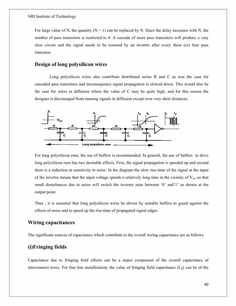
Design of long polysilicon wires
Long polysilicon wires also contribute distributed series R and C as was the case for
cascaded pass transistors and inconsequence signal propagation is slowed down. This would also be
the case for wires in diffusion where the value of C may be quite high, and for this reason the
designer is discouraged from running signals in diffusion except over very short distances.
For long polysilicon runs, the use of buffers is recommended. In general, the use of buffers to drive
long polysilicon runs has two desirable effects. First, the signal propagation is speeded up and second
there is a reduction in sensitivity to noise. In the diagram the slow rise-time of the signal at the input
of the inverter means that the input voltage spends a relatively long time in the vicinity of Vinv so that
small disturbances due to noise will switch the inverter state between ‘0’ and’1’ as shown at the
output point.
Thus , it is essential that long polysilicon wires be driven by suitable buffers to guard against the
effects of noise and to speed up the rise-time of propagated signal edges.
Wiring capacitances
The significant sources of capacitance which contribute to the overall wiring capacitance are as follows
(i)Fringing fields
Capacitance due to fringing field effects can be a major component of the overall capacitance of
interconnect wires. For fine line metallization, the value of fringing field capacitance (Cff) can be of the

NRI Institute of Technology
41
same order as that of the area capacitance. Thus , Cff should be taken into account if accurate prediction
of performance is needed.
Where l = wire length
t = thickness of wire
d = wire to substrate separation.
Then, total wire capacitance
Cw = Carea + Cff
(ii)Interlayer capacitances
From the definition of capacitance itself, it can be said that there exists a capacitance between the layers
due to parallel plate effects. This capacitance will depend upon the layout i.e., where the layers cross or
whether one layer underlies another etc., by the knowledge of these capacitances, the accuracy of circuit
modeling and delay calculations will be improved. It can be readily calculated for regular structures.
(iii) peripheral capacitance
1. The source and drain p-diffusion regions forms junctions with the n-substrate (or n-well) at well
defined and uniform depths.
2. Similarly, the source and drain n-diffusion regions forms junctions with p-substrate (or p-well) at
well defined and uniform depths.
3. Hence, for diffusion regions, each diode thus formed has associated a peripheral (side wall)
capacitance with it.
4. As a whole the peripheral capacitance,Cp will be the order of pF/unit length. So its value will be
greater than Carea of the diffusion region to substrate.

NRI Institute of Technology
42
Cp increases with reduction in source or drain area.
Total diffusion capacitance is
Cdiff = Carea + Cp
However, as the n and p-active regions are formed by impure implants at the surface of the silicon
incase of orbit processes, they have negligible depth. Hence Cp is quite negligible in them.
Typical values are given in tabular form
Typical values Diffusion capacitance
5µm 2µm 1.2µm
Area C (C area) 1.0 × 10⁻⁴pF/µm2 1.75 × 10⁻⁴pF/µm2 3.75 × 10⁻⁴pF/µm2
Periphery (Cperiph) 8.0 × 10⁻⁴pF/µm2 Negligible (assuming implanted
regions of negligible depth) negligible
Fan – in and Fan-out
Fan-in: The number of inputs to a gate is called as fan - in.
Fan-out: The maximum number of similar gates that a gate can drive while remaining within the
guaranteed specifications is called as fan-out.
Effects of Fan-in and Fan-out on propagation delay:
• An additional input to a CMOS logic gate requires an additional nMOS and pMOS i.e., two
additional transistors, while incase of other MOS logic gates, it requires one additional transistor.
• In CMOS logic gates, due to these additional transistors, not only the chip area but also the total
effective capacitance per gate also increased and hence propagation delay increases.
• Some of the increase in propagation delay time can be compensated by the size-scaling method.
• By increasing the size of the device, its current driving capability can be preserved.
NRI Institute of Technology
43
• Due to increase in both of inputs and devices size, the capacitance increases, Hence propagation
delay will still increase with fan-in.
• An increase in the number of outputs of a logic gate directly adds to its load capacitances. Hence,
the propagation delay increases with fan-out.
Choice of layers
The following are the constraints which must be considered for the proper choice of layers.
1. Since the polysilicon layer has relatively high specific resistance (RS), it should not be used for
routing VDD and VSS (GND) except for small distances.
2. VDD and GND (VSS) must be distributed only on metal layers, due to the consideration of Rs value.
3. The capacitive effects will also impose certain restrictions in the choice of layers as follows
(i) where fast signal lines are required, and in relation to signals on wiring which has relatively higher values of RS.
(ii) The diffusion areas have higher values of capacitance to substrate and are harder to drive.
4. Over small equipotential regions, the signal on a wire can be treated as being identical at all points.
5. Within each region the propagation delay of the signal will comparably smaller than the gate
delays and signal delays caused in a system connected by wires.
Thus the wires in a MOS system can be modeled as simple capacitors. This concept leads to the
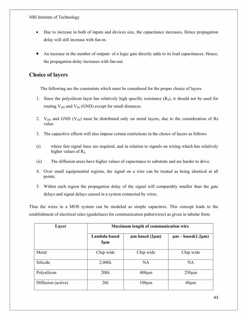
establishment of electrical rules (guidelines) for communication paths(wires) as given in tabular form.
Maximum length of communication wire Layer
Lambda based 5µm
µm based (2µm) µm – based(1.2µm)
Metal Chip wide Chip wide Chip wide
Silicide 2,000λ NA NA
Polysilicon 200λ 400µm 250µm
Diffusion (active) 20λ 100µm 60µm

NRI Institute of Technology
44


](https://img.dokumen.tips/doc/110x75/55cf8fe1550346703ba0ce6f/vlsi-technologymtech-1-1unit-3.jpg)


![[Chemistry] 2008 CSE Unit 4 Exam](https://img.dokumen.tips/doc/110x75/577cd9d21a28ab9e78a434b0/chemistry-2008-cse-unit-4-exam.jpg)