Embed Size (px)
Citation preview

Report EUR 26976 EN
Jan Paepen Magnus Gårdestig Per Reppenhagen Grim John Keightley Jonas Nilsson Kari Peräjärvi Olof Tengblad Harri Toivonen
2014
Critical parameters and performance
tests for the evaluation of digital data
acquisition hardware
Line

European Commission
Joint Research Centre
Institute for Reference Materials and Measurements
Contact information
Jan Paepen
Address: Joint Research Centre, Retieseweg 111, 2440 Geel, Belgium
E-mail: [email protected]
Tel.: +32 14 571329
ERNCIP Project Platform
https://erncip-project.jrc.ec.europa.eu/
JRC Science Hub
https://ec.europa.eu/jrc
Legal Notice
This publication is a Technical Report by the Joint Research Centre, the European Commission’s in-house science service.
It aims to provide evidence-based scientific support to the European policy-making process. The scientific output
expressed does not imply a policy position of the European Commission. Neither the European Commission nor any person
acting on behalf of the Commission is responsible for the use which might be made of this publication.
All images © European Union 2014
JRC93260
EUR 26976 EN
ISBN 978-92-79-44517-0 (PDF)
ISSN 1831-9424 (online)
doi:10.2788/66637
Luxembourg: Publications Office of the European Union, 2014
© European Union, 2014
Reproduction is authorised provided the source is acknowledged.
Abstract
Recent developments of digital data acquisition systems allow real-time pre-processing of detector signals at a high count
rate. These so-called pulse processing digitizers are powerful and versatile instruments offering techniques which are
important for nuclear security, critical infrastructure protection, nuclear physics and radiation metrology. Certain aspects
of digital data acquisition affect the performance of the total system in a critical way and therefore require special
attention. This report presents a short introduction to digital data acquisition, followed by a discussion of the critical
parameters which affect the performance in the lab and in the field. For some of the parameters, tests are proposed to
assess the performance of digital data acquisition systems. Good practices are offered to guide the selection and
evaluation of digital data acquisition systems. More general performance criteria which are not specifically related to
digital data acquisition systems are discussed separately.
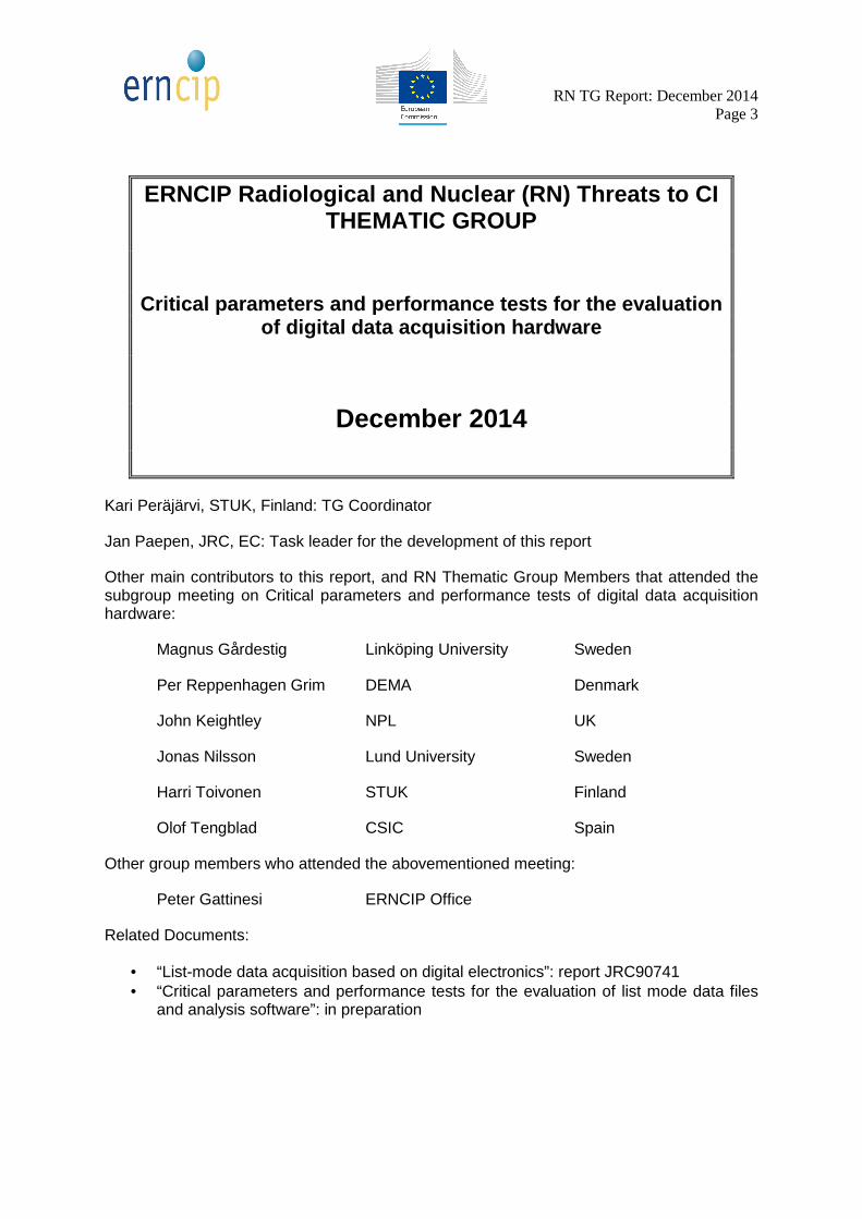
RN TG Report: December 2014 Page 3
ERNCIP Radiological and Nuclear (RN) Threats to CI
THEMATIC GROUP
Critical parameters and performance tests for the evaluation of digital data acquisition hardware
December 2014
Kari Peräjärvi, STUK, Finland: TG Coordinator
Jan Paepen, JRC, EC: Task leader for the development of this report
Other main contributors to this report, and RN Thematic Group Members that attended the subgroup meeting on Critical parameters and performance tests of digital data acquisition hardware:
Magnus Gårdestig Linköping University Sweden
Per Reppenhagen Grim DEMA Denmark
John Keightley NPL UK
Jonas Nilsson Lund University Sweden
Harri Toivonen STUK Finland
Olof Tengblad CSIC Spain
Other group members who attended the abovementioned meeting:
Peter Gattinesi ERNCIP Office
Related Documents:
• “List-mode data acquisition based on digital electronics”: report JRC90741 • “Critical parameters and performance tests for the evaluation of list mode data files
and analysis software”: in preparation

RN TG Report: December 2014 Page 4
Table of contents
EXECUTIVE SUMMARY ................................................................................................................... 6
1 INTRODUCTION TO DIGITAL DATA ACQUISITION ....................................................... 7
1.1 Acronyms ............................................................................................................................................7
1.2 First-stage electronics in a typical detector setup ................................................................................9
1.3 A basic digital data acquisition system with one detector ................................................................. 10
1.4 Advanced systems with multiple detectors ....................................................................................... 11
2 PERFORMANCE CRITERIA FOR DIGITAL DATA ACQUISITION, TESTS AND
GOOD PRACTICES .......................................................................................................................... 12
2.1 Tools to facilitate performance tests ................................................................................................. 12
2.1.1 Signal generators................................................................................................................................. 12
2.1.2 Analysis tools ....................................................................................................................................... 13
2.1.3 Standard format for list-mode data .................................................................................................... 13
2.2 Firmware algorithms ......................................................................................................................... 14
2.2.1 Firmware algorithm selection criteria ................................................................................................. 14
2.2.2 Types of firmware algorithms ............................................................................................................. 14
2.2.3 Detailed knowledge of firmware algorithms is required .................................................................... 15
2.3 Size and number of input channels ................................................................................................... 16
2.4 DC sampling frequency and bandwidth, input dynamic range and resolution ................................... 16
2.4.1 The sampling process and its limitations ............................................................................................ 16
2.4.2 Input dynamic range and resolution ................................................................................................... 17
2.5 Time resolution ................................................................................................................................. 17
2.6 Memory size and data throughput .................................................................................................... 18
2.7 Clock synchronization........................................................................................................................ 20
2.8 Clock overflow .................................................................................................................................. 20
2.9 Recording logic signals ...................................................................................................................... 21
2.10 Resistive feedback versus pulsed-reset preamplifiers ....................................................................... 21
2.11 Dead time and pulse pile-up.............................................................................................................. 23
3 GENERAL PERFORMANCE CRITERIA .............................................................................. 24
3.1 Connectors ........................................................................................................................................ 24
3.2 Immunity to vibrations ...................................................................................................................... 24
3.3 Leakage current noise caused by moisture ........................................................................................ 25

RN TG Report: December 2014 Page 5
3.4 Temperature effects and gain stabilisation ....................................................................................... 25
3.5 Supply of power in field operations................................................................................................... 26
3.6 High pulse rates................................................................................................................................. 27
3.7 Protection to harsh environments ..................................................................................................... 27
3.8 Displays ............................................................................................................................................. 27
REFERENCES .................................................................................................................................... 29

RN TG Report: December 2014 Page 6
Executive summary
This report has been produced by the ERNCIP Thematic Group on the Protection of Critical Infrastructure from Radiological and Nuclear Threats (RN TG), which is focussing on three subjects, with dedicated tasks related to each. Full details of the remit and tasks of the RN TG are available in the Work Programme of the RN TG.
• Task 1: List-mode data acquisition based on digital electronics • Task 2: Remote expert support of field teams • Task 3: Remote controlled radiation measurements and sampling using unmanned vehicles
As part of Task 1, this report deals with digital radiation detection systems employing data collection in "list-mode". This list-mode data can be stored locally for later analysis, or could be streamed to other locations for real-time processing including e.g. alarm generation. Task 1 will deliver 3 reports, as depicted in Figure 1.
Figure 1: Reports produced in the frame of ERNCIP RN, Task 1.
Recent developments of digital data acquisition systems allow real-time pre-processing of detector signals at a high count rate. These so-called pulse processing digitizers are powerful and versatile instruments offering techniques which are important for nuclear security, critical infrastructure protection, nuclear physics and radiation metrology [KEI, 2013]. Certain aspects of digital data acquisition affect the performance of the total system in a critical way and therefore require special attention. This report presents a short introduction to digital data acquisition, followed by a discussion of the critical parameters which affect the performance in the lab and in the field. For some of the parameters, tests are proposed to assess the performance of digital data acquisition systems. Good practices are offered to guide the selection and evaluation of digital data acquisition systems. More general performance criteria which are not specifically related to digital data acquisition systems are discussed separately.
The report only deals with performance tests with respect to the acquisition of list-mode data with digitizers (hardware). For a discussion on the performance tests of list mode data analysis software, the authors refer to the report "Critical parameters and performance tests for the evaluation of list mode data files and analysis software" (in preparation).
Critical parameters and performance tests for the
evaluation of digital data acquisition hardware
(this report)
Critical parameters and performance tests for the
evaluation of list mode data files and analysis
software (in preparation)
List-mode data acquisition
based on digital electronics
EUR 26715

RN TG Report: December 2014 Page 7
1 Introduction to digital data acquisition This introduction describes the typical electronics found in the first stage of a detector setup. The characteristics of the first-stage electronics determine to a great extend the type of digital algorithm used to process the detector signal and to extract the information of interest.
1.1 Acronyms
AC Alternating current
ADC An analog-to-digital converter (abbreviated ADC, A/D or A to D) is a device that converts a continuous physical quantity (usually voltage) to a digital number that represents the quantity's amplitude [Wikipedia].
CAMAC Computer Automated Measurement And Control (CAMAC) is a standard bus and modular crate electronics standard for data acquisition and control used in nuclear and particle physics experiments and in industry. The bus allows data exchange between plug-in modules [Wikipedia].
CFD Constant fraction discrimination
DAC Digital-to-analog converter
DAQ Data acquisition, data acquisition system. For simplification, the wording "digital data acquisition system" is often interchanged with "digitizer" or DAQ.
DC Direct current
DSP A digital signal processor (DSP) is a specialized microprocessor with an architecture optimized for the operational needs of digital signal processing, such as to measure (with its ADC), filter and/or compress continuous real-world analog signals [Wikipedia].
ELET Extrapolated leading edge threshold
ENOB Effective number of bits (ENOB) is a measure of the dynamic performance of an analog-to-digital converter (ADC) and its associated circuitry, taking into account the imperfections of the digitalisation process, such as noise and distortion [Wikipedia].
FET Field-effect transistor
FFT Fast Fourier transform
FPGA A field-programmable gate array (FPGA) is an integrated circuit designed to be configured by a customer or a designer after manufacturing. Contemporary FPGAs have large resources of logic gates and RAM blocks to implement complex digital computations [Wikipedia].
GSPS Gigasamples per second (1 GSPS = 109 s-1)
HPGe High-purity germanium detector
IR Infrared
LCD Liquid crystal display
LET Leading edge threshold
NIM Nuclear Instrumentation Module. The NIM standard defines mechanical and electrical specifications for electronics modules used in experimental particle and nuclear physics [Wikipedia].

RN TG Report: December 2014 Page 8
PCI, PCIe
PCI (Peripheral Component Interconnect) is a local computer bus for attaching hardware devices in a computer. PCIe (PCI Express) is a high-speed serial computer expansion bus standard designed to replace the older PCI [Wikipedia].
PMT A photomultiplier tube (PMT) is an electronic device that converts light (typically from a scintillator) to an electrical signal which is then amplified in multiple stages to as much as 100 million times. [Wikipedia]
PXI PCI eXtensions for Instrumentation (PXI) is one of several modular electronic instrumentation platforms in current use [Wikipedia].
RAM Random access memory
TTL Transistor–transistor logic (TTL) is a class of digital circuits built from bipolar junction transistors (BJT) and resistors [Wikipedia]. It defines the voltage levels of digital signals in order to be interpreted as logic "high" or logic "low".
USB Universal Serial Bus
UV Ultraviolet
VME VME (Versa Module Europa) is a computer bus standard, originally developed for the Motorola 68000 line of CPUs, but later widely used for many applications and standardized by the IEC as ANSI/IEEE 1014-1987 [Wikipedia].
ZLE Zero-length encoding
RN TG Report: December 2014 Page 9
1.2 First-stage electronics in a typical detector setup
In a typical detector setup, each detector is coupled to first-stage electronics that converts and/or amplifies the detector signal to a measurable quantity. Depending on the type of detector, one can typically distinguish two types of first-stage electronics.
Non-integrating first-stage electronics: For example, a photomultiplier tube (PMT) converting the light from a scintillator detector to an electric signal and then amplifying that signal. These types of electronics do not perform an integration of the electric signal. In ideal conditions, the integral of the signal pulse is proportional to the energy of the radiation.
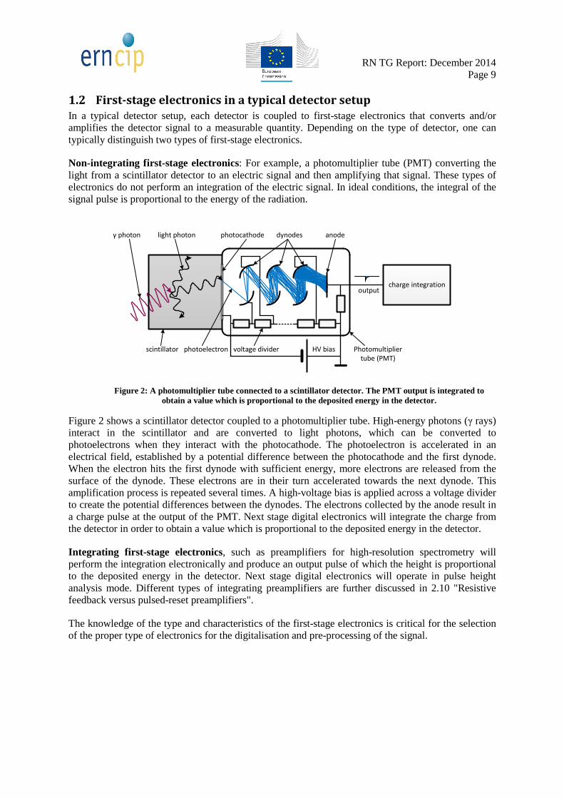
Figure 2: A photomultiplier tube connected to a scintillator detector. The PMT output is integrated to obtain a value which is proportional to the deposited energy in the detector.
Figure 2 shows a scintillator detector coupled to a photomultiplier tube. High-energy photons (γ rays) interact in the scintillator and are converted to light photons, which can be converted to photoelectrons when they interact with the photocathode. The photoelectron is accelerated in an electrical field, established by a potential difference between the photocathode and the first dynode. When the electron hits the first dynode with sufficient energy, more electrons are released from the surface of the dynode. These electrons are in their turn accelerated towards the next dynode. This amplification process is repeated several times. A high-voltage bias is applied across a voltage divider to create the potential differences between the dynodes. The electrons collected by the anode result in a charge pulse at the output of the PMT. Next stage digital electronics will integrate the charge from the detector in order to obtain a value which is proportional to the deposited energy in the detector.
Integrating first-stage electronics, such as preamplifiers for high-resolution spectrometry will perform the integration electronically and produce an output pulse of which the height is proportional to the deposited energy in the detector. Next stage digital electronics will operate in pulse height analysis mode. Different types of integrating preamplifiers are further discussed in 2.10 "Resistive feedback versus pulsed-reset preamplifiers".
The knowledge of the type and characteristics of the first-stage electronics is critical for the selection of the proper type of electronics for the digitalisation and pre-processing of the signal.
scintillator
photocathode
photoelectron
anodedynodes
HV bias
light photon
voltage divider
outputcharge integration
Photomultiplier
tube (PMT)
γ photon

RN TG Report: December 2014 Page 10
1.3 A basic digital data acquisition system with one detector
Modern digitizers perform pre-processing actions in real-time using electronic components like Field Programmable Gate Arrays (FPGAs) and Digital Signal Processors (DSPs). These components can be programmed after which they behave as digital electronics with a huge amount of logical gates and registers, one or more processors and on-chip memory. In fact, the "programs" can be code that will run on the processor, but also a description of the schematics of a large digital system. These programs are typically referred to as "firmware". The programmability of the digitizers has the advantage that the firmware, and so the behaviour of the component, can be changed without modifying the hardware.
Figure 3: Block diagram of a digital data acquisition system, after [WP2081].
Figure 3 represents a block diagram of a scintillator detector connected to a digitizer. The digitizer has the following parts:
• A wideband amplifier at the input that allows better use of the input dynamic range of the ADC. Some digitizers also have a DAC connected to the input of a differential input amplifier, allowing shifting the reference of the input signal up or down, before the ADC;
• An anti-aliasing filter to restrict the bandwidth of the signal to approximately satisfy the sampling theorem;
• An ADC that converts the signal to a stream of digital numbers representing the signal amplitude;
• Digital filters embedded as firmware in an FPGA/DSP to pre-process the digitized signal and extract the pulse characteristics;
• Memory to buffer the obtained pulse characteristics before they are read by the computer; • An interface for the communication with the host computer (USB, ethernet, optical, PCIe,
etc…) and for managing control signals such as external triggering and vetoes, clock propagation and synchronisation.
Digitizers continuously sample the input signal with a rate that can go up to a few GSPS (Gigasamples per second). Transferring the full waveform to the host computer would require an unrealistically high data throughput. To reduce the amount of data and lower the required throughput, digitizers have pulse processing firmware to extract only the relevant information about the detector pulses. The digital filters implemented in firmware perform very similarly with respect to conventional analog electronic modules, and provide pulse shaping, filtering, baseline restoration, extraction of timing information, pile-up reduction, etc. More complex pulse processing firmware extracts more information like the pulse rise and fall time, tail area and pulse shape characteristics. In addition to a dramatic reduction in the size of the electronic modules, the main advantage of digitally implemented filters is the greater flexibility and better performance, especially for applications involving higher count rates.
RN TG Report: December 2014 Page 11
Some digitizers can operate as waveform recorders. In this mode, the data stream from the ADC is directly transmitted to the computer. Due to the high sampling rate and limited throughput rate, this operating mode can only be sustained for a very short period of time, unless large parts of the stream are rejected, e.g. when the signal is below a certain threshold. The waveform recording mode provides maximum freedom in post-processing, but is only achievable for lower count rates.
1.4 Advanced systems with multiple detectors
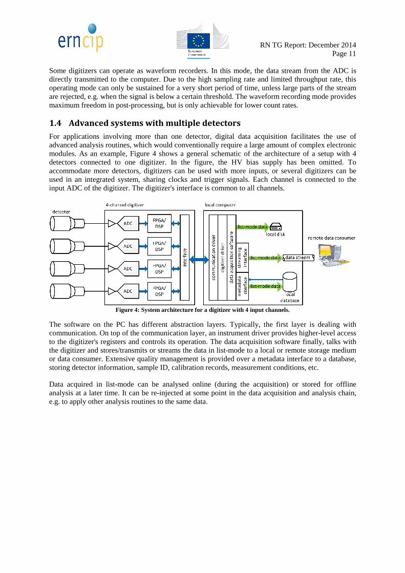
For applications involving more than one detector, digital data acquisition facilitates the use of advanced analysis routines, which would conventionally require a large amount of complex electronic modules. As an example, Figure 4 shows a general schematic of the architecture of a setup with 4 detectors connected to one digitizer. In the figure, the HV bias supply has been omitted. To accommodate more detectors, digitizers can be used with more inputs, or several digitizers can be used in an integrated system, sharing clocks and trigger signals. Each channel is connected to the input ADC of the digitizer. The digitizer's interface is common to all channels.
Figure 4: System architecture for a digitizer with 4 input channels.
The software on the PC has different abstraction layers. Typically, the first layer is dealing with communication. On top of the communication layer, an instrument driver provides higher-level access to the digitizer's registers and controls its operation. The data acquisition software finally, talks with the digitizer and stores/transmits or streams the data in list-mode to a local or remote storage medium or data consumer. Extensive quality management is provided over a metadata interface to a database, storing detector information, sample ID, calibration records, measurement conditions, etc.
Data acquired in list-mode can be analysed online (during the acquisition) or stored for offline analysis at a later time. It can be re-injected at some point in the data acquisition and analysis chain, e.g. to apply other analysis routines to the same data.

RN TG Report: December 2014 Page 12
2 Performance criteria for digital data acquisition, tests and
good practices Performance requirements of digitizers depend much on the application. In general, one could separate lab use from field use. In the controlled environment of a laboratory, issues with temperature stability, vibration, moisture, power supplies, high pulse rates etc. are usually not relevant when compared to field use. The application of radiation detectors in the field is mostly focussed on the detection of radiation, in contrary to precise and accurate measurements which usually require dedicated laboratories. For example, a typical issue with mobile detector systems in the field are variations of the background radiation due to the presence of NORM or washout effects caused by precipitation after a dry period. These fluctuations pose challenges for the alarming algorithms, which have to cope with the contradicting requirements of high detection sensitivity and low false alarm rate.
Future measurement systems may contain several different types of detector, not only ionising radiation detectors but including other sensors such as optical (UV, IR) and additional information about the measurement system such as occupancy sensors and interrogation beam on/off time.
The user should note the requirements of the application and build a digital data acquisition system accordingly. It might however be not so easy to specify these requirements and to address the critical parameters that affect the application. The following sections discuss different performance parameters which might become critical for some applications. Some ideas are presented on how to test the performance of a DAQ system on these parameters. The discussion might not be applicable to all situations and the listing is not intended to be complete. Instead, the document should be considered as a guide to assist in the selection of the most suitable digitizer and the evaluation of the most critical parameters for its application.
2.1 Tools to facilitate performance tests
Signal generators of different types are instruments which are very useful for the performance tests of digitizers, in addition to software tools for the analysis of the acquired data.
2.1.1 Signal generators
A simple waveform generator able to generate a repetitive signal can be used for simple tests, e.g. to verify that the total number of events counted matches the acquisition time and the signal frequency. It can also be convenient to check the maximum throughput that a data acquisition system can sustain.
More advanced arbitrary waveform generators can be used to reproduce the signal from a detector, with or without superimposed noise. Some dual channel generators (such as the Agilent 81160A or similar) can for example apply a delay between the channels, where the delay time is drawn randomly from a certain distribution. This feature is very practical when evaluating time resolution.
Precision pulse generators are designed to simulate detector signals, and typically generate a signal with either a pseudo-random or a fixed frequency. The pulse height of the output is very precisely controlled, which makes this instrument ideal to evaluate the digitizer's pulse height analysis performance and the linearity thereof.
Signals from a real detector are the closest to the real application, but are not always available in the early development stage of the system. The statistical nature of decay and the background radiation should be taken into account when comparing e.g. count rates, which makes it difficult to perform quick counting tests with low activity radioactive sources.

RN TG Report: December 2014 Page 13
2.1.2 Analysis tools
As discussed earlier, most digitizers provide a quantity representing the energy or charge deposited in the detector and the timestamp. Others can also provide values representing the pulse shape.
In addition to the commonly known energy histograms, time interval histograms are a valuable diagnostics tool. For a single channel, the time interval histogram is a histogram of the time interval between every detected pulse and the next one. The histogram is easily constructed from calculating the differences between each pair of consecutive timestamps.
Figure 5: Time interval histogram of a measurement of a 134Cs source in a NaI well detector, on a time scale from 0
to 1 ms.
Figure 6: Same histogram as previous figure, but on a scale from 0 to 25 µs.
The time intervals between two successive events in a Poisson process with rate λ are independent and identically distributed exponential random variables with parameter λ. As a consequence, the time interval histogram is described by e- λt. Figure 5 shows such histogram of a measurement of a 134Cs source in a NaI well detector. On a logarithmic scale, the slope of the line corresponds to – λ. In this case, λ = 1.6·104 s-1. Figure 6 is the same figure, but on a smaller time scale. The histogram shows no counts for dt < 1160 ns, the dead time of the system (in this case determined by the digitizer's pulse processing time). The peak around 1.5 µs is attributed to afterpulses from the scintillator or PMT.
For a detailed discussion on analysis software, the authors refer to the report "Critical parameters and performance tests for the evaluation of list mode data files and analysis software" (in preparation).
2.1.3 Standard format for list-mode data
List-mode data acquisition hardware and analysis tools would greatly benefit from a standardized data format for list-mode data. In-depth argumentation on the application and the benefits of a standard can be found in the report [EUR 26715], which contains proposal for a standard list-mode data format.

RN TG Report: December 2014 Page 14
2.2 Firmware algorithms
2.2.1 Firmware algorithm selection criteria
The most relevant criteria for the selection of the type of firmware algorithm are:
• The information needs of the application (timestamps, pulse height, pulse waveform, etc.); • The properties of the detector and the electronics at the previous stage in the
detector/electronics chain (charge integrating preamplifier, PMT base with or without preamplifier, resistive feedback versus reset-type preamp, etc.);
• The characteristics of the pulse to be processed (its shape, length, etc.) • The possibility to acquire logic signals; • User programmability of the firmware.
Often, the selection of electronics is a trade-off between time resolution, pulse height resolution, noise considerations and linearity.
2.2.2 Types of firmware algorithms
Different types of firmware algorithms are available to extract on-line only the values of interest characterising the detector signal:
• Pulse waveform recording: all samples describing a pulse are recorded and transferred. A pulse is defined as a collection of samples fulfilling certain criteria: e.g. larger than a certain threshold, within certain timing windows, etc1. This leads to some data reduction and retains maximum flexibility in processing on the host PC, but is limited to applications with a low count rate.
• Charge integration in a single time gate, resulting in a value corresponding to the charge deposited in the detector, in addition to the timestamp. Applied e.g. with a scintillator detector coupled to a PMT.
• Double gate charge integration allowing real-time pulse shape discrimination with respect to the type of radiation, in addition to deposited charge. This algorithm yields the timestamp and two values representing the charge integrated over two time gates with different length. Applied e.g. with scintillator materials offering gamma/neutron discrimination based on different pulse tail shapes.
• Digital pulse shaping and pulse height analysis, yielding a value proportional to the energy of the photon or particle detected, in addition to the timestamp. Conventional analog shaping electronics (semi-Gaussian, RC-CR, quasi-triangular, etc.) is implemented in firmware using variations of the digital algorithm developed originally by [JOR, 1994]. This technique is typically used in high-resolution gamma spectrometry with HPGe detectors.
• More advanced pre-processing algorithms extract additional characteristics from the acquired pulse, such as (see also Figure 7):
o Timestamp: e.g. the time at which the trigger occurred, with respect to the start of the acquisition, or a global time signal;
o Baseline level before the pulse Sb, e.g. the average (or a straight line fit) of a number of samples before the trigger;
o Pulse height H: maximum sample value with respect to the baseline Sb; o Rise time: the time required to reach the pulse maximum, with respect to the trigger
timestamp; o Peak time tp: bin number or time when the pulse reaches its maximum; o End time te: bin number or time when the pulse comes down to trigger level or a
certain fraction of the pulse height (as in the figure);
1 Sometimes these types of algorithms are called zero-length encoding or zero suppression.

RN TG Report: December 2014 Page 15
o Fast component QF of the pulse tail, obtained by summing the samples (with respect to the baseline) over a time window with length C starting from the peak time;
o Slow component QS of the pulse tail, obtained by summing the samples (with respect to the baseline) over the time window starting from the end of the fast window until the end time;
o Total charge deposited in the detector, obtained by summing all samples in the pulse (with respect to the baseline).
Figure 7: Pulse characteristics.
The knowledge of the pulse characteristics is especially useful for the characterisation of new or uncommon types or sizes of detectors. For example, the characterisation of large (3.5" x 8") LaBr3:Ce scintillator detectors, as described by [GIA, 2013], which shows that many properties of large detectors are not directly scalable from smaller ones.
Some digitizers allow the user to program the FPGA/DSP with customised firmware. However, this high level of flexibility comes at a cost as specialised knowledge is required to program digital electronics.
2.2.3 Detailed knowledge of firmware algorithms is required
It is obvious that the user should verify that the information delivered by the firmware (pulse characteristics, timestamp, etc.) is sufficient for the application, and that the information is provided with enough precision (related to the ADC sampling rate and resolution).
The knowledge of the operation of the firmware and its limitations can be essential to make optimal use of the digitizer's capabilities. For example, how does the firmware deal with ballistic deficit, with pole-zero cancellation, base-line restoration or pile-up rejection? Sections 2.4 through 2.11 will address some of these items that require special attention.
)( bF
p
p
SSQ
Ct
tt
t −= ∑+
=
∑+=
−=e
p
)( bS
t
Ctt
t SSQ

RN TG Report: December 2014 Page 16
2.3 Size and number of input channels
Modular crate or rack systems allow the integration of several digitizers into one system. Depending on the type (NIM, CAMAC, VME, PCI, PCIe, PXI, …), the rack provides power distribution to the modules, clock synchronisation and communication busses between modules and with the host PC. This high level of integration makes rack systems more suitable for applications that require many input channels, such as imaging with segmented detector arrays.
One example of such an application is the Advanced Gamma Tracking Array (AGATA), which requires accurate determination of the energy, time and position of every interaction as a γ-ray deposits its energy within the detector volume. AGATA expects to have an enormous impact on nuclear physics research in particular the exploration of nuclear structure at the extremes of isospin, mass, angular momentum, excitation energy and temperature. With the inception of the new generation of Radioactive Ion Beam (RIB) facilities, in the case of Europe FAIR (Darmstadt, Germany), HIE-ISOLDE (CERN, Geneva, Switzerland), SPIRAL2 (Caen, France) and SPES (Legnaro, Italy), where a much wider range of unstable proton- and neutron-rich nuclei will become accessible, a new era is being opened for nuclear physics experiments [AKK, 2012].
Desktop or stand-alone models are not part of a crate or rack system. They provide a cost-effective alternative to crate systems when the number of input channels in limited. As they are not installed in some kind of standardised crate, features like clock synchronisation, acquisition start/stop and data transfer to the host computer require special attention. In some cases, additional hardware is required to realise these features.
2.4 DC sampling frequency and bandwidth, input dynamic range and
resolution
2.4.1 The sampling process and its limitations
Sampling is the process of reducing a continuous signal to a sequence of discrete values or samples. The sampling frequency or sampling rate is defined as the number of samples obtained in one second. The sampling frequency should be high enough to be able to reconstruct the signal or at least properly represent the signal in a digital way. The Nyquist-Shannon sampling theorem states:
If a function x(t) contains no frequencies higher than B hertz, it is completely determined by giving its ordinates at a series of points spaced 1/(2B) seconds apart.
In general, the sampling frequency does not need to be much higher than the one obtained by frequency analysis of the signal and application of the Nyquist-Shannon theorem, as confirmed by e.g. [BEL, 2013] and [HEL, 2013]. Instead of increasing the sampling frequency, one should invest in digitizers with a higher resolution, which is proven to be more effective in achieving higher timing resolution.
The sampling is realised using an analog-to-digital converter (ADC), a device with various physical limitations, resulting in deviations from the theoretically perfect reconstruction, collectively referred to as distortion. Various types of distortion can occur, including:
• Aliasing. Only theoretical, infinitely long functions can have no frequency content above the Nyquist frequency. Therefore, some amount of aliasing is inevitable. Aliasing can be made arbitrarily small by increasing the order of the anti-aliasing filter. In a digital system, that increases the amount of arithmetic noise caused by numerical imprecision. Arithmetic noise has a flat spectral distribution, which is generally less disruptive than aliasing.
• Aperture error results from the fact that the sample is obtained as a time average within a sampling region, rather than just being equal to the signal value at the sampling instant. In a capacitor-based sample and hold circuit, aperture error is introduced because the capacitor cannot instantly change voltage thus requiring the sample to have non-zero width.
RN TG Report: December 2014 Page 17
• Jitter or deviation from the precise sample timing intervals. • Noise, such as thermal noise, detector leakage current noise, analog circuit noise, etc. • Slew rate limit error , caused by the inability of the ADC input value to change sufficiently
rapidly. • Quantization error as a consequence of the finite precision of words that represent the
converted values. Quantization error is directly related with resolution. For example, sampling with a 10-bit ADC results in 10-bit words, which can only take 210 = 1024 possible values.
• Error due to other non-linear effects of converting the input voltage to an output value (in addition to the effects of quantization).
2.4.2 Input dynamic range and resolution
The input dynamic range is the signal range that can be converted by the digitizer. The resolution (or bit-resolution) is the number of bits used by the ADC to represent the converted signal values. A limited resolution leads to quantization error, which can be reduced but not completely eliminated by oversampling (sampling at a higher frequency). The effect of oversampling is not high: an increase of the sampling frequency by a factor of four roughly corresponds with an increase of the resolution with 1 bit, as demonstrated by [FLA, 2013].
The resolution should be evaluated in function of the input dynamic range of the digitizer and the effective range of the signal. In principal, there are 2N signal levels for an N- bit conversion. However, as mentioned above, all real ADC circuits introduce noise and distortion, justifying the use of "effective number of bits" or ENOB. ENOB specifies the resolution of an ideal ADC circuit that would have the same resolution as the circuit under consideration. The wording "effective" is a bit misleading, as ENOB only relates to the ADC and associated electronics, assuming the use of the full input dynamic range. It is recommended to verify the statements of the manufacturer with respect to ENOB, as differences between the resolution and ENOB might be large [MIH, 2009].
Some digitizers have an additional differential amplifier at their input (before the ADC), which allows applying different gains and offsets to the input signal for better matching with the input dynamic range. Care should be taken when the input signal is out of the digitizer's range. High amplitude signals might distort the amplifier/filter at the input of the digitizer, which might result in longer dead times or secondary triggering of the signal when it recovers from the overshoot. Additional clipping electronics to be placed in front of the digitizer has been developed and proven to be successful [BOB, 2014]. The effect of high amplitude signals can be investigated by means of a waveform generator.
To investigate the signal range from the first-stage electronics, an oscilloscope with sufficient bandwidth can be used. To faithfully represent the signal, the input impedance of the oscilloscope shall match the impedance of the digitizer input.
2.5 Time resolution
The time resolution (or timing resolution) of a measurement setup reflects the ability to define precisely the moment of interaction of a particle or photon in the detector. The time resolution of the complete setup is determined by the time resolution of the individual parts (e.g. scintillator, PMT, electronics).
For applications where precise timing is required, it is important to know how the timestamp is extracted by the firmware. Some techniques yield timestamps which are depending on the pulse height (amplitude walk) or rise-time, while other techniques do not. Typical techniques are [KNO, 2000]:
• Timestamp corresponding to a certain threshold on the leading edge of the pulse (Leading Edge Threshold or LET);

RN TG Report: December 2014 Page 18
• Extrapolated Leading Edge Threshold (ELET), using two leading edge discriminators; • Timestamp corresponds to the time when the leading edge of the pulse reaches a fixed
(constant) fraction of the pulse height (Constant Fraction Discrimination or CFD); • Timestamp corresponding to the time the pulse has reached its maximum; • Timestamp corresponding to the zero crossing of second derivative versus time of rising edge
of the pulse (crossover timing).
A waveform generator can be used to determine the time resolution of a digitizer without the additional contribution of the detector and associated electronics. A pulse waveform representing the detector signal can be generated at a certain pulse rate, while the pulse rate (or frequency) is modulated with e.g. Gaussian noise. The width of the peak in the time interval histogram corresponding to the pulse period should then represent the standard deviation set in the modulator.
The constant fraction discrimination (CFD) algorithms used in digitizers have an improved time response compared to conventional CFDs when used with large HPGe detectors, as shown by [MIH, 2007].
2.6 Memory size and data throughput
Event rates can vary several orders of magnitude, depending on the application. Systems with large detectors as e.g. used in security applications can easily reach event rates in the order of millions per second. The limitations on memory size and data throughput of digitizers can be an issue for large event rates.
The digitizer's memory should be sufficiently large to deal with short bursts of events, and the data throughput (and storage) rate to the host PC shall be sufficient to cope with the incoming event rate.
In the event that the digitizer's memory cannot be emptied in time, data will be lost or the acquisition will be stopped (whatever fits the application). Means should be foreseen for the software to monitor the status of the digitizer's memory, in order to take proper action when data is lost. The full memory condition should not block the communication or other operational aspects of the digitizer. The time stamp clock for example shall keep on incrementing at its normal rate.
It is recommended to be careful with the interpretation of the maximum data throughput claimed by manufacturers of digitizers. The required throughput should be evaluated in function of the application. The achievable throughput on a particular computer system can be much lower than claimed by the manufacturer due to various reasons. The throughput also depends on the size and configuration of the data blocks. Quasi repetitive signals, e.g. from a detector placed in a pulsed beam, might require another memory configuration in order to achieve maximum throughput, as compared with random signals from measurements of a radioactive source.
Testing the maximum throughput of a digital data acquisition system can be done by the following means:
• With artificially created pulses from a pulse waveform generator; • Using artificially created pulses by a pseudo-random pulser; • With real signals from a fast detector and a radioactive source with sufficient activity.
A useful tool is the construction of a time interval histogram; a histogram of the time difference of every pulse with its predecessor. The time interval histogram of a repetitive signal should only contain one narrow line or peak at the abscissa corresponding with the pulse period. Figure 8 shows the time interval histogram on a log ordinate scale obtained from a repetitive signal with a period of 34.5 µs, corresponding to a frequency of about 29 kHz. The figure was constructed using the root data analysis framework developed and maintained by CERN [http://root.cern.ch].

RN TG Report: December 2014 Page 19
Figure 8: Time interval histogram of a 29 kHz repetitive signal.
The "Underflow" and "Overflow" values on the graph are both 0, indicating that all events are shown. Most events are at the correct time interval of T = 34.5 µs. However, 9 events appear at 2T, witnessing nine times one missed trigger. The 16 events below T are due to triggers in the noise, or to electrical spikes of some source. There are no events higher than 2T, meaning that there were no gaps in the data acquisition due to full memory conditions. Indeed, a full memory condition would lead to much larger gaps, as can be observed from Figure 9, constructed from a periodic signal with a frequency of 120.4 kHz. The period is 8.3 µs, which corresponds to the vertical line close to 0.
Figure 9: Time interval histogram for 120.4 kHz test (scale in µs), showing gaps in the data acquisition.
Simply "counting" the number of events from a repetitive signal acquired over a fixed amount of time enables to calculate back the frequency of the signal, which should match with the frequency set on the generator.
0.1
1
10
100
1000
10000
100000
1e+006
1e+007
0 500 1000 1500 2000 2500 3000 3500 4000
'dump_024_TIVd.dat'

RN TG Report: December 2014 Page 20
Figure 10: Time interval distribution of artificiall y created data representing an acquisition time of 100 s of a source with decay rate of 10000 /s. 5 µs of extended dead time is imposed on the data.
With a random pulser simulating the statistical nature of radioactive decay or with real measurements with a source, the time interval histogram will show an exponential decay (Figure 10). The statistical nature of the decay process makes data processing a bit more complicated. Nevertheless, these tests are required to take into account the statistical effects, e.g. short term fluctuations of number of events.
2.7 Clock synchronization
Certain applications require more than one digitizer because of the large number of detectors, but also because of the use of different types of detectors in the same system which might require digitizers with different firmware. Synchronisation of the digitizers requires not only the propagation of a master clock or reference clock (traceable to the SI-unit second if necessary), but also the distribution of a signal indicating the start and end of the acquisition. For ultimate precision, phase adjustments should be applied to correct for different propagation delays (different cable lengths, etc.) to the different channels, e.g. as in [AN2086].
Another method of synchronization involves sampling of a reference analog signal [BAR, 2007], but requires modifications to the firmware and additional hardware. In their approach, a switch is connected to every digitizer's input, allowing the selection of the detector signal or an analog reference signal, distributed to all digitizers. With PMT's, one could use a pulsed light source to include differences in signal propagation times in the part of the chain before the digitizer.
2.8 Clock overflow
Timestamps are obtained from the digitizer's clock counter, which is typically incremented at the sample rate. Clock overflow occurs when the value of the clock counter reaches its maximum and starts again from zero. For example, digitizers with a sample rate of 1 GSPS and a 32-bit clock counter will increment the counter every nanosecond, resulting in a clock overflow every 232·1 ns = 4.2 s.
As long as the count rate is high enough, clock overflow can be detected and corrected for by the instrument driver or data acquisition software. For low count rates however, overflow could occur an unknown number of times in-between two successive events, losing the ability for correction. Manufacturers should provide means to correct or detect overflow, or use larger data formats, which is however at the expense of throughput.

RN TG Report: December 2014 Page 21
A simple solution that barely affects throughput rates from digitizer to computer is to insert a special flag in the data stream to indicate an overflow. This way, the instrument driver running on the computer can keep track of the number of clock overflows n since the beginning of the acquisition. The driver can then and add a value of n·2b·T to each timestamp (b being the bit-depth of the counter and T the period at which it increments) and store the timestamp it in longer data format, e.g. 64-bit as being proposed [EUR 26715].
2.9 Recording logic signals
Certain applications require the recording of the timestamps associated with transitions of a logic signals from an external source, such as occupancy sensors, beam on/off signals or trigger or enable signals. The type of signal (TTL, NIM, or other) and impedance shall be considered. The digitizer shall be able to record these transitions, e.g. detect the rising or falling edge of a TTL signal, or the rising edge and the pulse width.
2.10 Resistive feedback versus pulsed-reset preamplifiers
Detector setups for high-resolution spectrometry such as HPGe detectors typically use integrating first-stage electronics, as depicted in Figure 11. The charge collected by the detector is amplified and integrated over a capacitor CF placed in the feedback loop of the amplifier.
Figure 11: A charge sensitive preamplifier connected to a semiconductor detector. The gain of the amplifier is determined by the feedback capacitor. The resistor allows discharging the capacitor. Alternatively, a
switch-type device can be used to remove the charge (pulsed reset).
Resistive feedback preamplifiers have a resistor placed in parallel with the feedback capacitor CF to remove the charge. A large resistor R is required to minimise noise and to have a good charge to amplitude conversion. Indeed, the signal-to-noise improves by the square root of R [GRA, 1995]. The resulting pulse decay time is much larger than the width of the detector signal (Figure 12), resulting in a larger probability for pulse pile-up at higher count rates. Next stage electronics needs to shape the signal to a Gaussian-like pulse, whose amplitude is proportional to the energy of the radiation.
reset-type
resistive
feedback-type
CF
R
S
semiconductor
detector
HV bias
fet output
pulse height
analysis

RN TG Report: December 2014 Page 22
Figure 12: Typical output of a resistive feedback preamplifier.
Pulsed-reset preamplifiers are often employed with detectors for X-ray spectrometry because they have better noise performance due to the elimination of the feedback resistor. In gamma-ray spectrometry, they allow higher counting rates than resistive feedback preamplifiers. Pulsed-reset preamplifiers will integrate the charge from the detector and produce a step output (Figure 13). The height of the step is proportional to the integrated charge from one event. In addition to the charge steps from interactions in the detector, the charge will slowly increase due to the leakage current of the detector. The charge on the feedback capacitor - and also the output voltage - will continue to increase until a certain threshold has been reached. Then, the charge will be removed by closing a transistor operated as a switch (transistor-reset), or by providing an optical pulse to the preamp input stage FET (pulsed optical). This reset mechanism results in a fast but large transition of the output voltage, after which the next-stage electronics needs some time to recover. During recovery, the detector system is dead. For this reason, reset-type preamplifiers often have a logic inhibit output pulse with adjustable width that will disable the ADC during reset and recovery. The reset mechanism will add an extra source of dead time.
Figure 13: Output of a pulsed-reset preamplifier.
Not all digitizers for pulse-height-analysis are able to process the signal from pulsed-reset preamplifiers since the signal sits on a ramp, or they cannot deal with the inhibit output pulse. The latter could be solved by separate digitalisation of the inhibit pulse connected to another input channel of the digitizer. This way, software can properly deal with the resets.
output voltage
time0 V
step height
corresponds to
deposited
energy
output voltage
time0 V
reset resetslope due to
leakage current
step height
corresponds to
deposited
energy

RN TG Report: December 2014 Page 23
2.11 Dead time and pulse pile-up
Digitizers are often advertised as allowing "dead-time-less acquisition", even though a clear description of the meaning of this wording is not always given. There can be several sources of dead time introduced by the digitizer:
• Dead time associated with every pulse, caused by the digitizer's pulse processing time. Compared with conventional electronics, digitizers typically have a much shorter pulse processing time. This results in a much shorter dead time and a reduction of pulse pile-up, which effectively increases the detection efficiency [MIH, 2007].
• Dead time caused by limited memory size and data throughput. • When pulsed reset preamplifiers are used: dead time associated with the reset time and
required recovery time of the amplifier/filter in the digitizer's input stage. • Dead time associated with the digitizer's input stage recovery after being exposed to large
signals, e.g. originating from cosmic radiation detected in large volume detectors.
These sources of dead time are not necessary present for all types of digitizers. Accurate activity measurements require the application of dead-time corrections, for which the knowledge of the amount and type of dead time is essential. Some sources of dead time can depend on the settings of the digitizer, e.g. the length of the charge integration gate. Manufacturers should provide a clear explanation of different sources of dead time, and users are strongly advised to scrutinise the effect of dead time in the case when accurate measurements are to be performed.
At high count rates, when the time between two pulses is short, there is a risk that they are recorded as a single pulse at a distorted energy. Consequences of this pulse pile-up are a net loss of counts and the assignment of piled-up events to the wrong energy, causing a distortion of the spectrum [SAB, 2014].
The option to detect and correct for pile-up depends on the time between the pulses:
• When the second pulse sits on the tail of the first, it is usually possible to process both pulses correctly. All information can be obtained, but some characteristics might not be reliable;
• When the second pulse starts around the time when the first reaches its maximum, pile-up can still be detected, but correct processing is not possible;
• When the rising edges are overlapping, the pile-up can't be detected and consequently both pulses are treated as one.
In all cases, a special pile-up flag shall indicate what type of pile-up has been detected so that data processing algorithms can properly deal with pulse pile-up.
The effect of pulse pile-up and the different sources of dead time can be assessed experimentally, using the signal generators discussed earlier. A step-wise approach starting with a simple test and gradually increasing the complexity is highly recommended, as the combination of the different sources of dead time and pulse pile-up can become difficult to untangle and correct for in real applications.

RN TG Report: December 2014 Page 24
3 General performance criteria The performance criteria listed in this section do not relate to digital data acquisition equipment specifically, but can be valid for any type of equipment used in the field of radiation detection and measurement.
3.1 Connectors
While digital data acquisition systems do not have the knobs, dials and switches found in conventional analog electronics, they will always have connectors which can affect the long-term reliability of a data acquisition system. Connectors are used for:
• Supply of electrical power; • Communication between modules or to a host PC; • Analog signal inputs for detector signals; • Analog outputs for signal monitoring, testing, etc.; • Digital inputs/outputs for triggering; • Digital inputs/outputs for clock synchronisation (might be optical); • Digital inputs/outputs for synchronisation of acquisition start and stop; • Additional digital inputs/outputs of which the functioning is flexible and can be programmed.
For signal connections, it is important to consider:
• Type of connector; • Impedance; • Differential inputs or single ended inputs; • Signal polarity; • Active high or active low digital signals.
To avoid accidental loss of the connections, they are preferably realised with secured connectors (screwed, locked, …). A reliable connection is especially important for modules that have a build-in high voltage generator to bias the detector or photomultiplier.
3.2 Immunity to vibrations
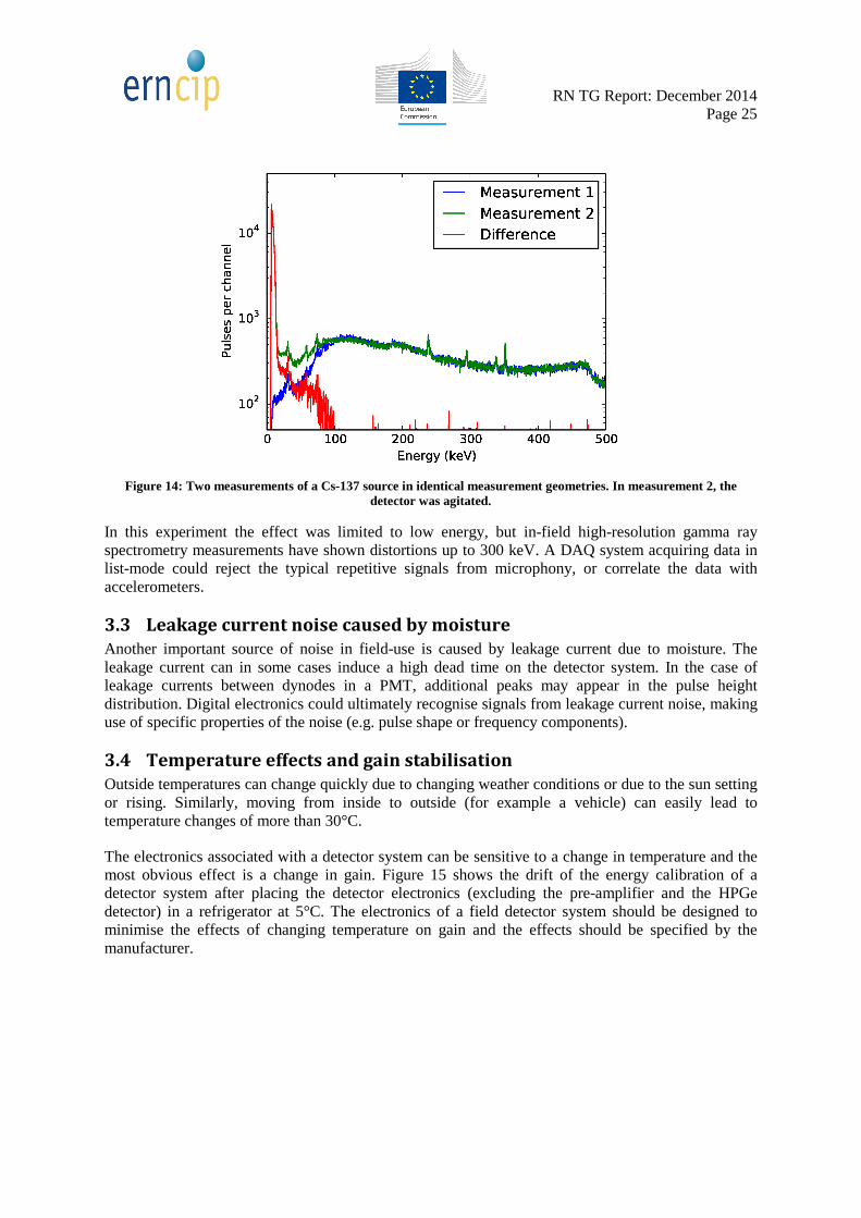
In field use, vibrations affect the performance of the detector system. These effects are typically called "microphony". The exact process is difficult to understand, and might be caused by the inductions of phonons in the detector system or a change in capacitance between wires as they move [KOC, 2010]. This kind of microphony mainly manifests itself as noise in the low energy (below 100 keV) part of a pulse height distribution though there can be other effects. Figure 14 demonstrates the effect of microphony on a HPGe detector. An energy histogram of a 137Cs source was measured twice with the same detector. In measurement 2, the detector was agitated, resulting in a large distortion at low energy.
RN TG Report: December 2014 Page 25
Figure 14: Two measurements of a Cs-137 source in identical measurement geometries. In measurement 2, the detector was agitated.
In this experiment the effect was limited to low energy, but in-field high-resolution gamma ray spectrometry measurements have shown distortions up to 300 keV. A DAQ system acquiring data in list-mode could reject the typical repetitive signals from microphony, or correlate the data with accelerometers.
3.3 Leakage current noise caused by moisture
Another important source of noise in field-use is caused by leakage current due to moisture. The leakage current can in some cases induce a high dead time on the detector system. In the case of leakage currents between dynodes in a PMT, additional peaks may appear in the pulse height distribution. Digital electronics could ultimately recognise signals from leakage current noise, making use of specific properties of the noise (e.g. pulse shape or frequency components).
3.4 Temperature effects and gain stabilisation
Outside temperatures can change quickly due to changing weather conditions or due to the sun setting or rising. Similarly, moving from inside to outside (for example a vehicle) can easily lead to temperature changes of more than 30°C.
The electronics associated with a detector system can be sensitive to a change in temperature and the most obvious effect is a change in gain. Figure 15 shows the drift of the energy calibration of a detector system after placing the detector electronics (excluding the pre-amplifier and the HPGe detector) in a refrigerator at 5°C. The electronics of a field detector system should be designed to minimise the effects of changing temperature on gain and the effects should be specified by the manufacturer.
RN TG Report: December 2014 Page 26
Figure 15: Cs-137 centroid position as a function of time after the detector electronics was put in a refrigerator at a temperature of 5°°°°C.
Besides effects such as a change in pulse rate and temperature (affecting the scintillator crystal), there are several other effects that can change the gain of a detector system, such as variations in the local magnetic field. For this reason, a detector system for field use should have a gain stabilisation function. The algorithm for how the gain stabilisation works should be specified and it should be possible to turn it on or off.
3.5 Supply of power in field operations
For a detector system to be usable in the field, it must have a battery. The battery should be able to supply the system with power for several hours and it should preferably be possible to change the battery for extended use in the field. An extra backup battery or super capacitor for short time operation while the battery is changed is also useful in field applications. Specifications for operating the electronics of a detector system under battery power should be provided by the manufacturer. This includes expected battery operation time in high and low temperature environments.
Commonly, field teams use a vehicle from which they operate. The vehicle can be used as a recharging station for computers and electronics. Recharging the equipment is usually done through the use of power supplies which run on mains voltage (230 or 110 V AC). In their turn, the power supplies are powered by the 12 V DC from the vehicle by the use of DC to AC power inverters. A similar setup is usually used in car-borne detector systems. Many power inverters do not supply a mains voltage AC sine wave but instead use a square wave to supply power. The high frequency component of the square wave is not always properly filtered by the power supply and can cause noise in the measurements (see Figure 16). Mobile power generators can also be a source of noise which can distort pulse height distributions. A detector system for field use should be tested by the manufacturer for sensitivity to noise in the power supply. Preferably, the DAQ should be powered directly from the vehicle's 12 V DC power, eliminating the need of an inverter.

RN TG Report: December 2014 Page 27
Figure 16: Two measurements of a Cs-137 source on a HPGe detector, in identical measurement geometries. In measurement 2, the computer collecting data from the detector and powering the detector was powered by a square
wave AC power supply.
When digitizers are used, the analysis of the time interval distribution of pulses can be helpful to assess the susceptibility of interference with mains power.
3.6 High pulse rates
The pulse rate in a detector system used for mobile gamma spectrometry can experience several orders of magnitude difference in pulse rate due to different amounts of deposited radioactivity after an accident or encountering a high activity radioactive source. This change in pulse rate can affect the energy calibration of the detector system [GIA, 2013]. The electronics of a field detector system should be insensitive to gain change due to a change in pulse rate and specifications for this parameter should be specified by the manufacturer. It is recognised that a detector system can not handle arbitrarily high pulse rates. It should be able to recognise and warn the user of the situation when the pulse rate is too high to provide reliable results.
3.7 Protection to harsh environments
Doing field measurements can be harsh on the equipment and the detector electronics. Exposure to moisture, dust and mechanical shock is common. The electronics should for this reason be water and dust tight. It should also be possible to drop it from a small height without damage. Connectors should be ruggedized as much as possible taking into consideration the connecters used in most detector systems today. It should be possible to cover the connectors when not in use so as to facilitate decontamination of the equipment. Resistance to moisture, dust and mechanical force should be specified by the manufacturer. If connection between two devices is lost due to mechanical shock or cables being cut, the electronics should be constructed so as to protect itself from damage due to the improper disconnection.
3.8 Displays
As field measurements are done in both low light conditions and in direct sun light, displays and indicator lights should be readable in both cases. Displays should have a backlight and low glare properties whereas indicator lights should output enough light to be clearly visible in all conditions. The intensity of the backlight and indicator lights should preferably be adjusted automatically through the use of an ambient light sensor so as to minimise battery drain and maximise low light vision of the operator.

RN TG Report: December 2014 Page 28
LCD displays have tendency to stop operating at low temperatures as the mobility of the crystals in the LCD decreases with temperature. If the instrument uses a display, its low temperature operation characteristics should be specified by the manufacturer. If the instrument is expected to be used in a cold environment, it should be fitted with a suitable display.

RN TG Report: December 2014 Page 29
References [AKK, 2012] Akkoyun, S., et al., AGATA - Advanced GAmma Tracking Array, Nuclear Instruments and Methods in Physics Research A, 668 (2012) 26-58
[AN2086] Synchronization of CAEN digitizers in Multiple Board Acquisition Systems, CAEN Application Note AN2086, 9 May 2013
[BAR, 2007] Bardelli, et al., An efficient method for timing synchronization between many digital sampling channels, Nuclear Instruments and Methods in Physics Research A 572 (2007) 882–892
[BEL, 2013] Belli, et al., A study on the pulse height resolution of organic scintillator digitized pulses, Fusion Engineering and Design 88 (2013) 1271– 1275
[BOB, 2014] Bobin, Bouchard, Thiam, Ménesguen, Digital pulse processing and optimisation of the front-end electronics for nuclear instrumentation, Applied Radiation and Isotopes 87 (2014) 195-199
[EUR 26715] Kari Peräjärvi, John Keightley, Jan Paepen, Olof Tengblad, Harri Toivonen, List-mode data acquisition based on digital electronics, European Commission report EUR 26715 EN, JRC90741, ISBN 978-92-79-38985-6, ISSN 1831-9424, doi:10.2788/88299
[FLA, 2013] Flaska, et al., Influence of sampling properties of fast-waveform digitizers on neutron-gamma-ray pulse-shape discrimination for organic scintillation detectors, Nuclear Instruments and Methods in Physics Research A 729 (2013) 456–462
[GIA, 2013] A. Giaz, L. Pellegri, S. Riboldi, F. Camera, N. Blasi, C. Boiano, A. Bracco, S. Brambilla, S. Ceruti, S. Coelli, F. C. L. Crespi, M. Csatlòs, S. Frega, J. Gulyàs, A. Krasznahorkay, S. Lodetti, B. Million, A. Owens, F. Quarati, L. Stuhl, and O. Wieland, Nuclear Instruments and Methods in Physics Research A 729 (2013) 910–921
[GIA, 2014] Giaz, A., et al., Characterization of large volume 3.5" x 8" LaBr3:Ce detectors, Nuclear Instruments and Methods in Physics Research A 729 (2013) 910–921
[GRA, 1995] Graeme, Gerald G, Photodiode amplifiers: op amp solutions, McGraw-Hill, New York, ISBN 0-07-024247-X (1995)
[HEL, 2013] Hellesen, et al., Impact of digitization for timing and pulse shape analysis of scintillator detector signals, Nuclear Instruments and Methods in Physics Research A 720 (2013) 135–140
[JOR, 1994] Jordanov, Knoll, Digital Synthesis of pulse shapes in real time for high resolution radiation spectroscopy, Nuclear Instruments and Methods A 345 (1994) 337
[KEI, 2013] Keightley, et al., Recent Advances in Digital Coincidence Counting for Radionuclide Metrology, 3rd International Conference on Advancements in Nuclear Instrumentation Measurement Methods and their Applications (ANIMMA), 2013, IEEE
[KNO, 2000] Knoll, Radiation Detection and Measurement, third ed., Wiley, New York, USA (2000)
[KOC, 2010] P. Kock, “Investigating microphonic noise in mobile gamma-spectrometric HPGe measurements using accelerometers,” in Third European IRPA Congress 2010 June 14-16, Helsinki, Finland, (Helsinki), June 2010
RN TG Report: December 2014 Page 30
[MIH, 2007] L.C. Mihailescu, C. Borcea, A.J.M. Plompen, Data acquisition with a fast digitizer for large volume HPGe detectors, Nuclear Instruments and Methods in Physics Research A 578 (2007) 298-305
[MIH, 2009] Mihailescu, et al., Investigations for the use of the fast digitizers with C6D6 detectors for radiative capture measurements at GELINA, Nuclear Instruments and Methods in Physics Research A 600 (2009) 453-459
[SAB, 2014] Sabbatucci, L., et al., Multi-shape pulse pile-up correction: The MCPPU code, Radiation Physics and Chemistry 104 (2014) 372-375
[WP2081] Digital Pulse Processing in Nuclear Physics, CAEN White Paper WP2081, 26 August 2011

Europe Direct is a service to help you find answers to your questions about the European Union
Freephone number (*): 00 800 6 7 8 9 10 11
(*) Certain mobile telephone operators do not allow access to 00 800 numbers or these calls may be billed.
A great deal of additional information on the European Union is available on the Internet.
It can be accessed through the Europa server http://europa.eu.
How to obtain EU publications
Our publications are available from EU Bookshop (http://bookshop.europa.eu),
where you can place an order with the sales agent of your choice.
The Publications Office has a worldwide network of sales agents.
You can obtain their contact details by sending a fax to (352) 29 29-42758.
European Commission
EUR 26976 EN – Joint Research Centre – Institute for Reference Materials and Measurements
Title: Critical parameters and performance tests for the evaluation of digital data acquisition hardware
Author(s): Jan Paepen, Magnus Gårdestig, Per Reppenhagen Grim, John Keightley, Jonas Nilsson, Kari Peräjärvi,
Olof Tengblad, Harri Toivonen
Luxembourg: Publications Office of the European Union
2014 – 32 pp. – 21.0 x 29.7 cm
EUR – Scientific and Technical Research series – ISSN 1831-9424
ISBN 978-92-79-44517-0 (PDF)
doi:10.2788/66637

ISBN 978-92-79-44517-0
doi:10.2788/66637
JRC Mission
As the Commission’s
in-house science service,
the Joint Research Centre’s
mission is to provide EU
policies with independent,
evidence-based scientific
and technical support
throughout the whole
policy cycle.
Working in close
cooperation with policy
Directorates-General,
the JRC addresses key
societal challenges while
stimulating innovation
through developing
new methods, tools
and standards, and sharing
its know-how with
the Member States,
the scientific community
and international partners.
Serving society
Stimulating innovation
Supporting legislation
LB
-NA
-26
97
6-E
N-N