Embed Size (px)
Citation preview
EE 3110 Microelectronics I Suketu Naik
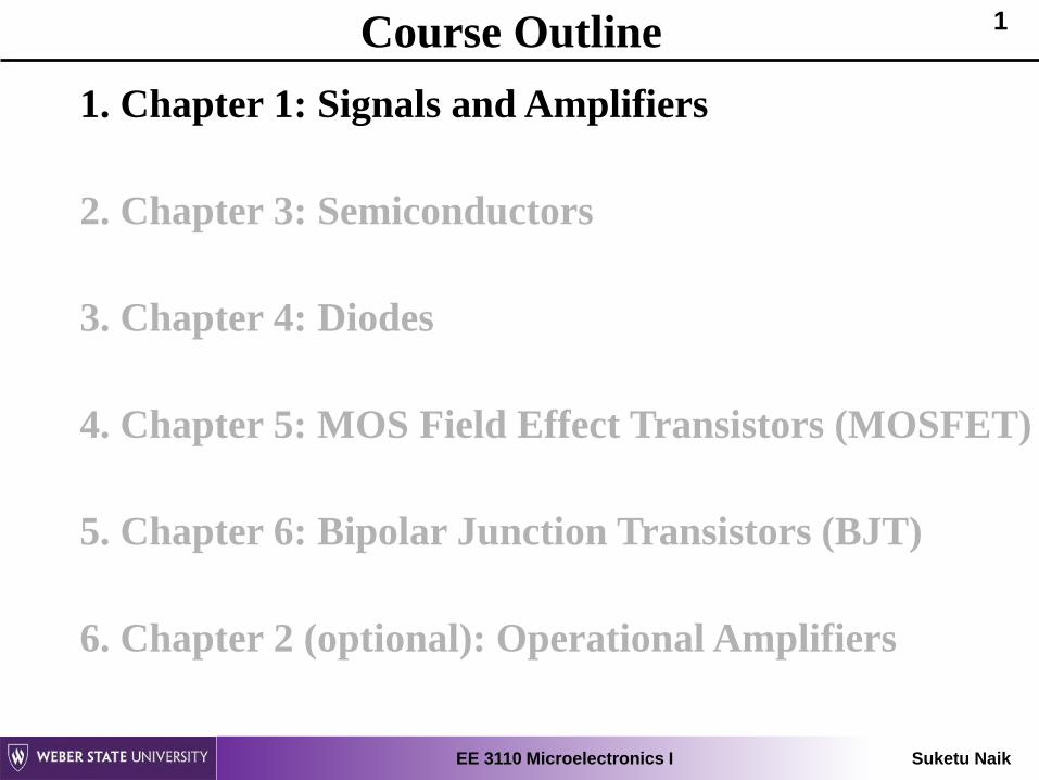
1Course Outline
1. Chapter 1: Signals and Amplifiers
2. Chapter 3: Semiconductors
3. Chapter 4: Diodes
4. Chapter 5: MOS Field Effect Transistors (MOSFET)
5. Chapter 6: Bipolar Junction Transistors (BJT)
6. Chapter 2 (optional): Operational Amplifiers
EE 3110 Microelectronics I Suketu Naik
2
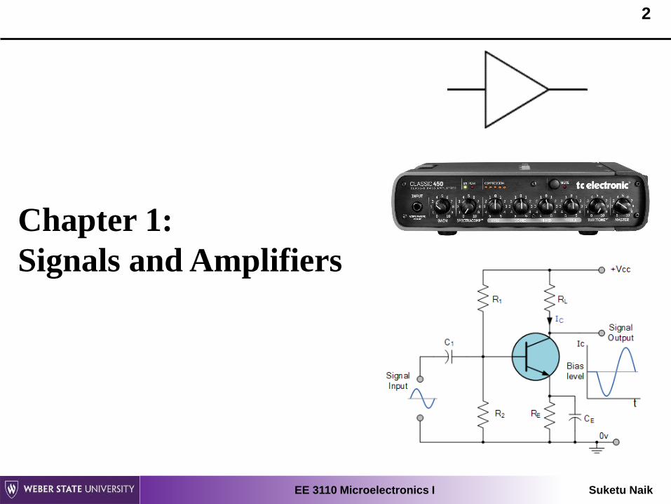
Chapter 1:
Signals and Amplifiers
EE 3110 Microelectronics I Suketu Naik
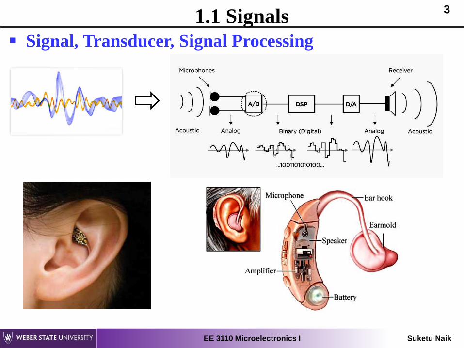
31.1 Signals
Signal, Transducer, Signal Processing
EE 3110 Microelectronics I Suketu Naik
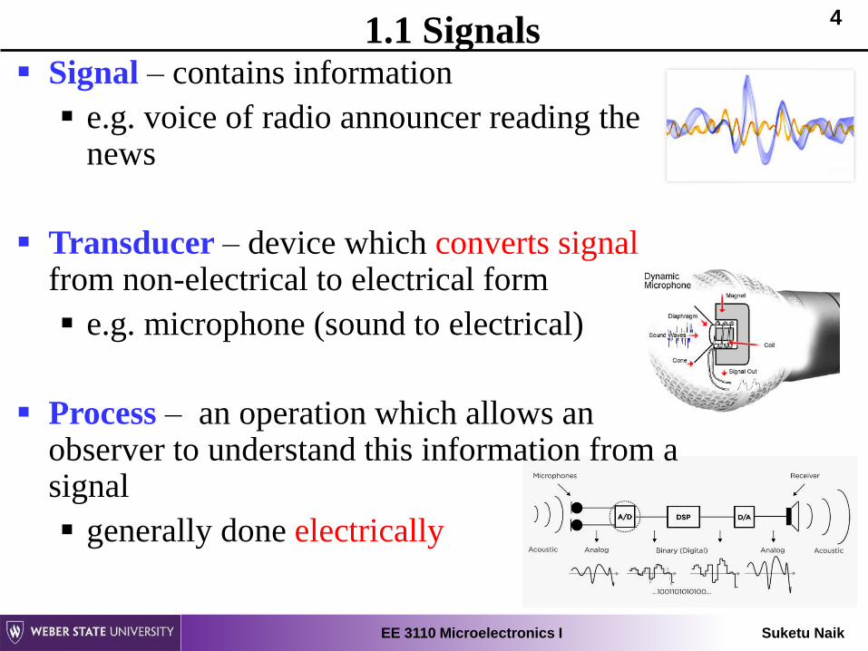
41.1 Signals
Signal – contains information
e.g. voice of radio announcer reading the news
Transducer – device which converts signalfrom non-electrical to electrical form
e.g. microphone (sound to electrical)
Process – an operation which allows an observer to understand this information from a signal
generally done electrically

EE 3110 Microelectronics I Suketu Naik
5Analog Circuit Design 101
Both art and engineering
Minimize expensive components
Maximize circuit robustness
Insensitive to part selection
Insensitive to operating environment
Know that semiconductor devices
1) Are highly nonlinear
2) Are sensitive to temperature changes
3) Can vary from part to part (matching issue)

EE 3110 Microelectronics I Suketu Naik
6Introduction [1/2]
Chapter Summary
Electronic circuits process signals, and thus understanding electrical signals is essential
Thevenin and Norton representations of signal sources
The representation of a signal as sum of sine waves
The analog and digital representations of a signal

EE 3110 Microelectronics I Suketu Naik
7Introduction [2/2]
Chapter Summary
Most basic and pervasive signal-processing function: signal amplification, and correspondingly, the signal amplifier
Amplifiers are characterized (modeled) as circuit building blocks independent of their internal circuitry
How the frequency response of an amplifier is measured, and how it is calculated

EE 3110 Microelectronics I Suketu Naik
81.1. Signals
Figure 1.1: Two alternative representations of a signal source: (a) the
Thévenin form; (b) the Norton form.

EE 3110 Microelectronics I Suketu Naik
9Thevenin and Norton Equivalent Sources
Consider two source / load combinations to upper-right.
note that output resistance of a source limits its ability to deliver a signal at full strength
Q (a): what is the relationship between the source and output when maximum power is delivered?
for example, vs < vo? vs > vo? vs = vo?
Q (b): what are ideal values of RS for thevenin and norton representations?

EE 3110 Microelectronics I Suketu Naik
10Time and Frequency Domain
Figure 1.5 A symmetrical
square-wave signal of
amplitude V
Figure 1.6 The frequency
spectrum (also known as
the line spectrum) of the
periodic square wave of
Fig. 1.5.
Periodic Signals Discrete Spectra

EE 3110 Microelectronics I Suketu Naik
111.2 Frequency Spectrum of Signals
Frequency spectrum – defines the a time-domain signal
in terms of the strength of harmonic components
Q: What is a Fourier Series?
A: An expression of a periodic function as the sum
of an infinite number of sinusoids whose frequencies
are harmonically related

EE 3110 Microelectronics I Suketu Naik
12
0
1
Fourier Series Representation of ( )
1 ( ) ( )
1 ( ) ( )
( ) ( ) (
, 0
,
)2
1
k kk
k
k
x
a x kx d
ax a kx b kx
nx
b x k nx dx
f
f cos
f cos sin
f sin
Decomposition – of a periodic function into the
(possibly infinite) sum of simpler oscillating functions
What is a Fourier Series?

EE 3110 Microelectronics I Suketu Naik
131.2 Frequency Spectrum of Signals
Q: Can the Fourier Transform be applied to a non-periodic
function of time?
A: Yes, however (as opposed to a discrete frequency
spectrum) it will yield a continuous spectrum…

EE 3110 Microelectronics I Suketu Naik
141.3 Analog and Digital Signals
analog signal
discrete-time signal
is continuous with respect
to both value and time
is continuous with respect to value
but sampled at discrete points in time

EE 3110 Microelectronics I Suketu Naik
151.3 Analog and Digital Signals
Digital signal – is quantized (applied to values) as well as
sampled at discrete points in time

EE 3110 Microelectronics I Suketu Naik
161.4 Amplifiers
Q: Why is signal amplification needed?
A: Because many transducers yield output at low power
levels (mW or nW)
Linearity – is property of an amplifier which ensures a
signal is not “altered” from amplification
Distortion – is any unintended change in output

EE 3110 Microelectronics I Suketu Naik
171.4.1 Signal Amplification
Voltage amplifier – is used to boost voltage levels for
increased resolution.
Power amplifier – is used to boost current levels for
increased “intensity”.
output / input relationship for amplifier
( ) ( )o v it A tv v
voltage gain

EE 3110 Microelectronics I Suketu Naik
181.4.4 Power and Current Gain
Q: What is one main difference between an amplifier
and transformer? (both alter voltage levels)
A: Amplifier may be used to boost power delivery
( ) ( )
( )L o o
p
I i i
load power P v ipower gain A
input power P v i
EE 3110 Microelectronics I Suketu Naik
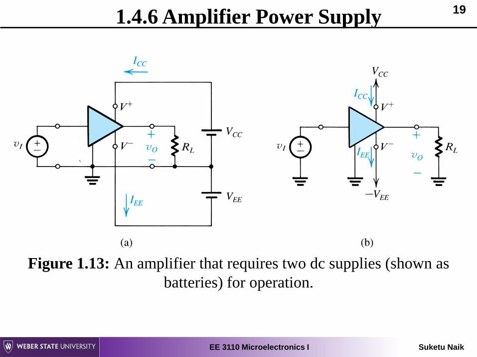
191.4.6 Amplifier Power Supply
Figure 1.13: An amplifier that requires two dc supplies (shown as
batteries) for operation.

EE 3110 Microelectronics I Suketu Naik
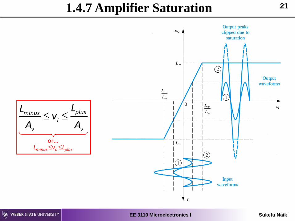
201.4.7 Amplifier Saturation
Limited linear range – practically, amplifier operation
is linear over a limited input range
Saturation – beyond this input range, saturation
occurs.
output remains constant as input varies
harmonic distortion occurs
power supply limitation
EE 3110 Microelectronics I Suketu Naik
211.4.7 Amplifier Saturation
or...minus o plus
plusminusi
v v
L v L
LLv
A A

EE 3110 Microelectronics I Suketu Naik
221.5 Circuit Models for Amplifiers
Model – is the description of component's (e.g. amplifier)
terminal behavior
neglecting internal operation / transistor design
values of the model parameters are found by
measurements and analysis

EE 3110 Microelectronics I Suketu Naik
231.5.1 Voltage Amplifiers
model of amplifier input terminals
sourcevolt.
source andinput
resistances
input vo tag )l e ( ii s
i s
Rv v
R R
model of amplifier output terminals
open-cktoutput
output andvoltageload
resistances
output vo (l )tage Lo vo i
L o
Rv A v
R R
Figure 1.16 (b): voltage amplifier with input signal source

EE 3110 Microelectronics I Suketu Naik
241.5.1 Voltage Amplifiers
Q: What is the “problem” with this model?
A: Gain (ratio of vo and vs) is not constant, and
dependent on input and load resistance.
sourcevolt.
source and output andinput load
resistances resistances
open-ckt output voltage
( ) i L i Lo vo s vo s
i s L o i s L o
R R R Rv A v A v
R R R R R R R R
The ideal amplifier model neglects this nonlinearity.
EE 3110 Microelectronics I Suketu Naik
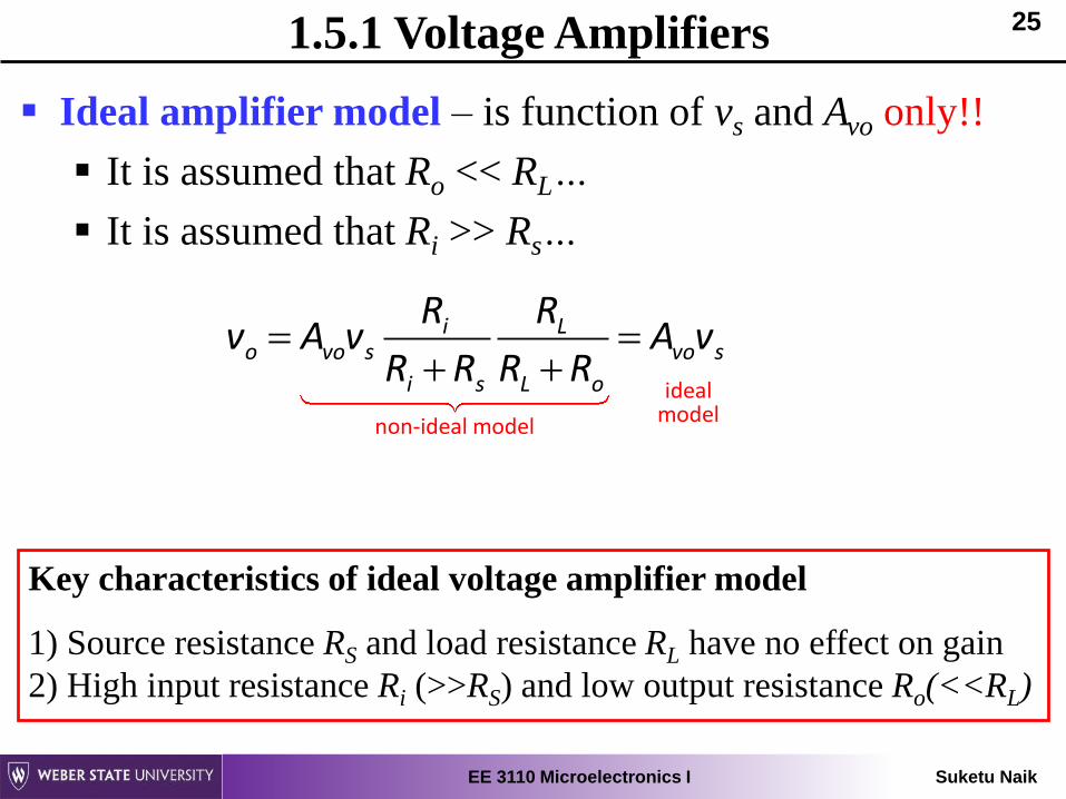
251.5.1 Voltage Amplifiers
Ideal amplifier model – is function of vs and Avo only!!
It is assumed that Ro << RL…
It is assumed that Ri >> Rs…
idealmodel
non-ideal model
i Lo vo s vo s
i s L o
R Rv A v A v
R R R R
Key characteristics of ideal voltage amplifier model
1) Source resistance RS and load resistance RL have no effect on gain
2) High input resistance Ri (>>RS) and low output resistance Ro(<<RL)

EE 3110 Microelectronics I Suketu Naik
26Example 1.3: Cascaded Amplifier Configurations
Figure 1.17: Three-stage amplifier for Example 1.3.
• High Input Resistance
• Modest Gain
• Low Input Resistance
• High Gain
• Low Output Resistance
• Unity Gain

EE 3110 Microelectronics I Suketu Naik
27Example 1.3: Cascaded Amplifier Configurations
Figure 1.17: Three-stage amplifier for Example 1.3.
aggregate amplifier with gain
Lv
s i s
vA
v i R

EE 3110 Microelectronics I Suketu Naik
281.5.3 Amplifier Types
voltage amplifier current amplifier
0
00
0
with 0
i
v
oi i
RvA
Rv
0
00
0
0 with
i
v
oi v
RiA
Ri
open circuit voltage gain short circuit current gain

EE 3110 Microelectronics I Suketu Naik
291.5.3 Amplifier Types
transconductance amp. transresistance amp.
0
0
0
with i
m
oi v
RiG
Rv
0
0
0
0 with
0i
m
oi i
RvR
Ri
short circuit
transconductance
open circuit
transresistance
EE 3110 Microelectronics I Suketu Naik
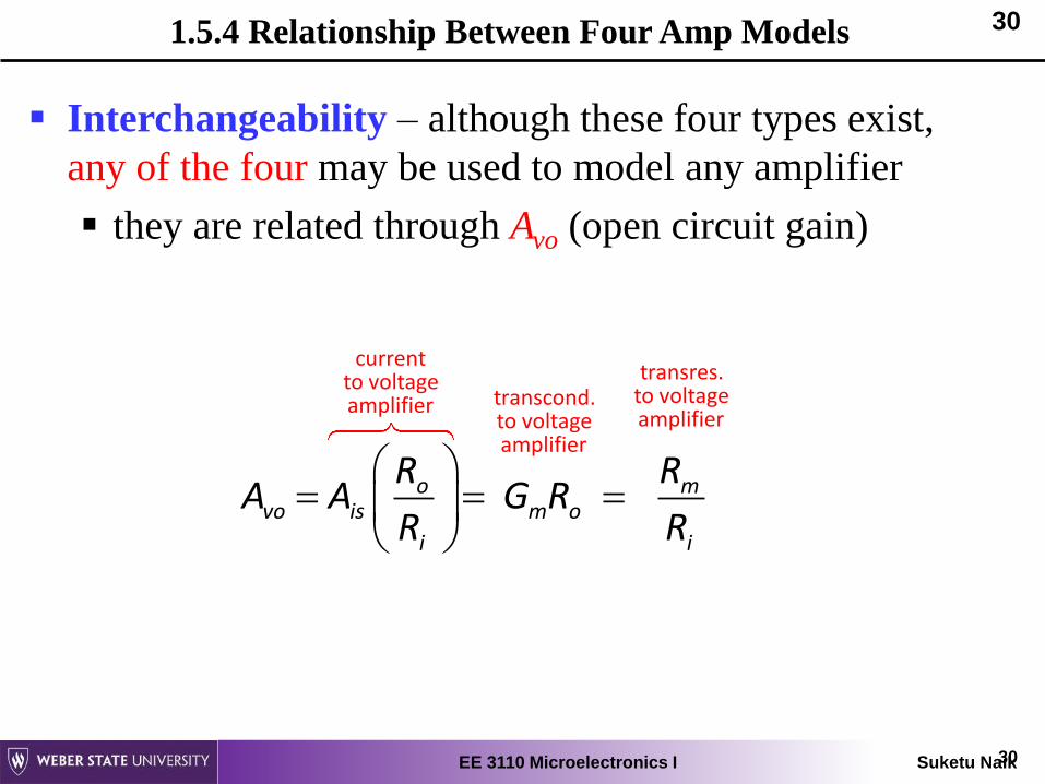
301.5.4 Relationship Between Four Amp Models
Interchangeability – although these four types exist,
any of the four may be used to model any amplifier
they are related through Avo (open circuit gain)
currenttransres.to voltage
to voltagetranscond.amplifieramplifierto voltage
amplifier
o mvo is m o
i i
R RA A G R
R R
30

EE 3110 Microelectronics I Suketu Naik
311.5.5 Determining Ri and Ro
Q: How can one calculate input resistance from terminal behavior?
A: Observe vi and ii, calculate via Ri = vi / ii
Q: How can one calculate output resistance from terminal behavior?
A:
Remove source voltage (such that vi = ii = 0)
Apply voltage to output (vx)
Measure negative output current (-io) or current going into the output terminal as ix
Calculate via Ro = -vx / io = vx / ix
31
EE 3110 Microelectronics I Suketu Naik
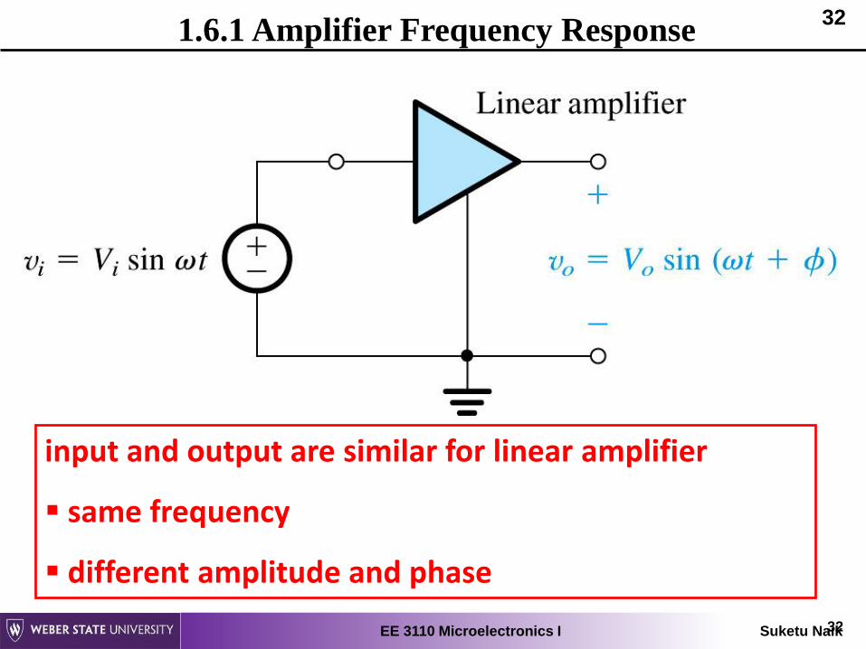
321.6.1 Amplifier Frequency Response
input and output are similar for linear amplifier
same frequency
different amplitude and phase
32

EE 3110 Microelectronics I Suketu Naik
331.6.1 Amplifier Frequency Response
Amplifier transfer function (T) – describes the
input-output relationship of an amplifier – or other
device – with respect to various parameters, including
frequency of input applied.
It is a complex value, often defined in terms of
magnitude and phase shift.
phase shift
magnitude gain
( ) )and ( o
i
V
V T T

EE 3110 Microelectronics I Suketu Naik
341.6.2 Amplifier Bandwidth
Q: What is bandwidth of a device?
A: The range of frequencies over which its magnitude
response is constant (within 3dB).
Q: For an amplifier, what is main bandwidth concern?
A: That the bandwidth extends beyond range of
frequencies it is expected to amplify.

EE 3110 Microelectronics I Suketu Naik
351.6.4 Single Time-Constant Networks
Figure 1.22: Two examples of STC networks: (a) a low-pass
network and (b) a high-pass network.
Amplifier's frequecy response can be categorized as low or high
pass filters

EE 3110 Microelectronics I Suketu Naik
36
Figure: Low-Pass Filter Magnitude (top-left) and Phase (top-right) Responses as well as High-Pass Filter (bottom-
left) and Phase (bottom-right) Responses
Frequency Response
EE 3110 Microelectronics I Suketu Naik
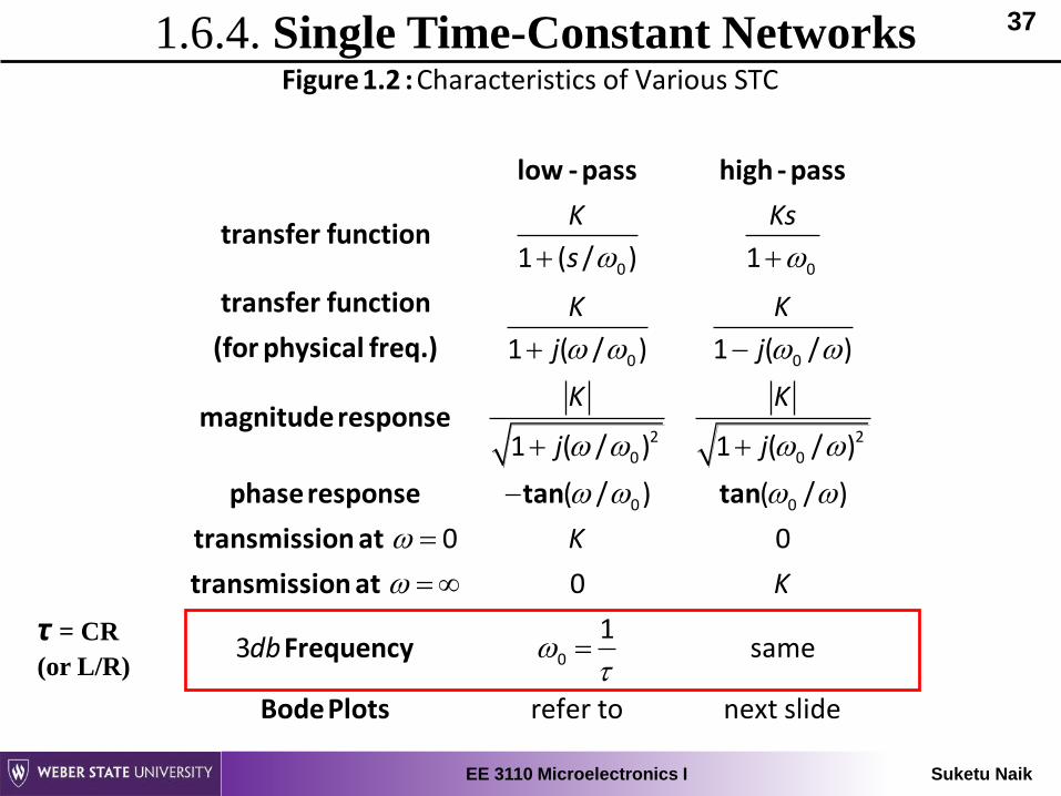
371.6.4. Single Time-Constant Networks
0 0
0 0
2 20 0
Characteristics of Various STC
1 ( / ) 1
1 ( / ) 1 ( / )
1 ( / ) 1 ( / )
K Ks
s
K K
j j
K K
j j
Figure 1.2 :
low - pass high - pass
transfer function
transfer function
(for physical freq.)
magnitude response
phase respon 0 0
0
( / ) ( / )
0 0
0
13 same
refer to next slide
K
K
db
se tan tan
transmission at
transmission at
Frequency
Bode Plots
τ = CR
(or L/R)

EE 3110 Microelectronics I Suketu Naik
38Example 1.5: Voltage Amplifier
Examine voltage amplifier with:
input resistance (Ri), input capacitance (Ci), gain factor (m), output resistance (Ro)
(a): Derive an expression for the amplifier voltage gain
Vo / Vs as a function of frequency. From this, find expressions for the dc gain and 3dB frequency.

EE 3110 Microelectronics I Suketu Naik
391.6.5 Classification of Amps Based on Frequency Response
Internal capacitances – cause the falloff of gain at high
frequencies (previous example)
Coupling capacitors – cause the falloff of gain at low
frequencies
are placed in between amplifier stages
generally chosen to be large