Embed Size (px)
Citation preview

Appendix to D2.1 Confidential additional information to provide some
background and detail not to be published outside the confines of the COSIGN project
Grant Agreement No. 619572
COSIGN
Combining Optics and SDN In next Generation data centre
Networks
Tim Durrant Venture Photonics Ltd
August 2015
Ref. Ares(2015)3601946 - 01/09/2015

Confidential notes as Appendix to D2.1
August 2015
This pack of information is to provide additional information regarding the Deliverable 2.1
The main focus of this appendix is the Venture switch technology. It provides some history of the technical development over the span of COSIGN so far, and also some recent testing that is directly or indirectly in support of D2.1. There is technical information on the product and processing under development that is to be treated as Confidential, only for members of the consortium (including the Commission Services).
Summary
“Integration of OpenFlow SW Interface with Polatis System and Venture 4x4 OXS”

Confidential notes as Appendix to D2.1
August 2015
The fundamental intent of the Venture Photonics part of the COSIGN project is the development of a fast solid state single mode InP Optical CrossPoint Switch (OXS) Key target characteristics are • Optical switching 5 ns • Wavelength window 1530-1560 nm • Polarisation dependent loss 1 dB • Insertion loss < 7 dB • Cross talk -50 dB Device to be capable of integration with driver circuit to be driven by OpenFlow software
Intent of Task 2.2.2 activities

Confidential notes as Appendix to D2.1
August 2015
The structure of the OXS project is such that • Much of the chip development effort is channelled through UNIVBRIS, though
much of the materials spend is from Venture • The packaging effort is provided by Venture • The driver and software integration effort is provided by DTU and UNIVBRIS • Additional support from TUE
Partner roles
There is a chip and package development, a driver development and an integration of optics with driver and software

Confidential notes as Appendix to D2.1
August 2015
The packaging solution developed using the CFP2 module style
Chip
Ribbon fibre/chip interface

Confidential notes as Appendix to D2.1
August 2015
Functionality of a 4x4 InP OXS chip
4 single-mode fibre interface 4 single-mode fibre interface
Contacts for switch drivers and optical monitors
Contacts for switch drivers and optical monitors and
thermistor
16 switches as an array
Chip dimensions are 5.0 x 5.5 mm
Location for thermistor

Confidential notes as Appendix to D2.1
August 2015
The basic principle of operation is by Active Vertical Coupling (AVC) Epi layers designed so that light passes straight through the switch with bias off. Switching occurs by carrier injection induced index matching change (bias on). This ‘lifts’ the optical path ‘up’, to then be internally reflected, then ‘dropped’ back to a different waveguide
Individual switch function
In addition Semiconductor Optical Amplifiers (SOA) and optical monitors are built into the waveguide to be able to give individual control of light conditions through the switch
Confidential notes as Appendix to D2.1
August 2015
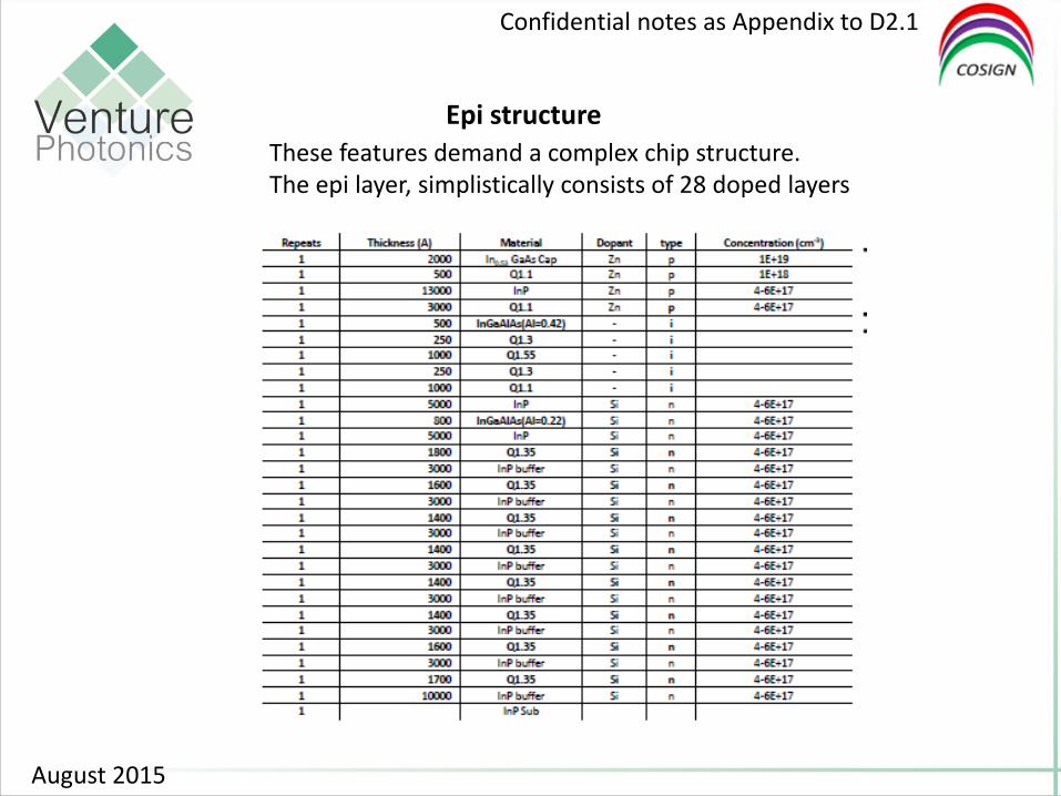
These features demand a complex chip structure. The epi layer, simplistically consists of 28 doped layers
Epi structure

Confidential notes as Appendix to D2.1
August 2015
Processing the wafer requires (in simplified form) 34 process steps, many needing very accurate alignment with previous activities. This is not including the cleaving and Anti-Reflection (AR) coating stages.
Wafer processing

Confidential notes as Appendix to D2.1
August 2015
S-inclined SOA Chip 2 mm*5 mm
L-inclined SOA Chip 2.2 mm*5 mm
1X1 OXS Chip 2 mm*5 mm
Laser Chips 1.1 mm*5 mm
As part of the risk mitigation approach for the wafer fabrication, test pieces are designed into the mask in addition to the OXS chips
Wafer design
Confidential notes as Appendix to D2.1
August 2015
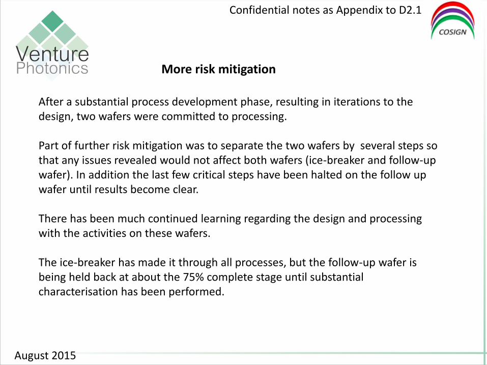
After a substantial process development phase, resulting in iterations to the design, two wafers were committed to processing. Part of further risk mitigation was to separate the two wafers by several steps so that any issues revealed would not affect both wafers (ice-breaker and follow-up wafer). In addition the last few critical steps have been halted on the follow up wafer until results become clear. There has been much continued learning regarding the design and processing with the activities on these wafers. The ice-breaker has made it through all processes, but the follow-up wafer is being held back at about the 75% complete stage until substantial characterisation has been performed.
More risk mitigation
Confidential notes as Appendix to D2.1
August 2015
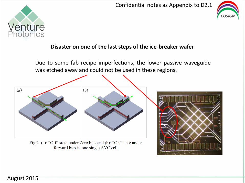
Due to some fab recipe imperfections, the lower passive waveguide was etched away and could not be used in these regions.
Disaster on one of the last steps of the ice-breaker wafer

Confidential notes as Appendix to D2.1
August 2015
However the region with upper active and lower passive structure is still intact in the Active Vertical Coupling (AVC) structure. This is true for all such layers present across the wafer.
Hope

Confidential notes as Appendix to D2.1
August 2015
• The material structure across the wafer is the same • This means that by cleaving the wafer carefully in a slightly different way we can use
some of the test pieces to perform characterisation of optical and integration performance in a representative way
• The key and only significant difference to a full OXS chip is that it is a single linear switch rather than a 4x4 switch with all the optics on one face
• The result of this is that the developed packaging cannot be used for this early characterisation work
• So the characterisation work is done on a lab alignment rig with reduced temperature control opportunities
• This has resulted in some of the measurements being done with ~50 mA rather that the planned ~250 mA
• Control of the chip switching function is the same regardless of the optical interface • There will not be opportunity for very fast switching characterisation as a result of the
packaging and jigging considerations. But full integration can be demonstrated under controlled conditions.
Logical consideration

Confidential notes as Appendix to D2.1
August 2015
697 µm
Good Facet Good Facet Fresh Good Facet
Bad Facet
Parts of the wafer being used

Confidential notes as Appendix to D2.1
August 2015
Recovery To test the switch on and off
1) Align the lensed fibre to the upper active region from the facet in the left hand side
2) Align the lensed fibre to the lower passive region from the facet in the right hand side
3) Inject light to the chip from the left lensed fibre, and detect the light power from the right lensed fibre
4) In this method, when the chip is under current injection, the light transmitted in the upper active waveguide injected from the left lensed fibre will be coupled into the lower passive waveguide.
Side view
Top view

Confidential notes as Appendix to D2.1
August 2015
The switch “Off” state can be defined with no power output in the right lensed fibre while the switch “On” state is defined with power detected in it; and the switch extinction ratio is defined as the 10*log10(Power_on/Power_off) The whole OXS extinction ratio is estimated to be 2*10*log10(Power_on/Power_off) Thus we can treat these test pieces as a switch In addition a number of other characteristics can be gathered.

Confidential notes as Appendix to D2.1
August 2015
Alignment rig and Device under test (Venture)
Detector system
FPGA/Driver (DTU)
Open Flow software (UNIVBRIS)
Laser light source
Lab set up for integration testing
With help from Bob Musk of Entroptix Ltd

Confidential notes as Appendix to D2.1
August 2015
Optical alignment
Confidential notes as Appendix to D2.1
August 2015
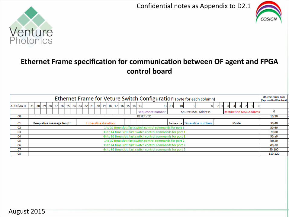
Ethernet Frame specification for communication between OF agent and FPGA control board

Confidential notes as Appendix to D2.1
August 2015
Wireshark snapshots of frames between Agent and FPGA
Agent to FPGA Install flow
FPGA to Agent confirmation
Agent to FPGA Uninstall flow
FPGA to Agent confirmation

Confidential notes as Appendix to D2.1
August 2015
Signal Tap snapshots of frames received by the FPGA
Install flow frame
Uninstall flow frame
Change of configuration
Change of configuration
Confidential notes as Appendix to D2.1
August 2015
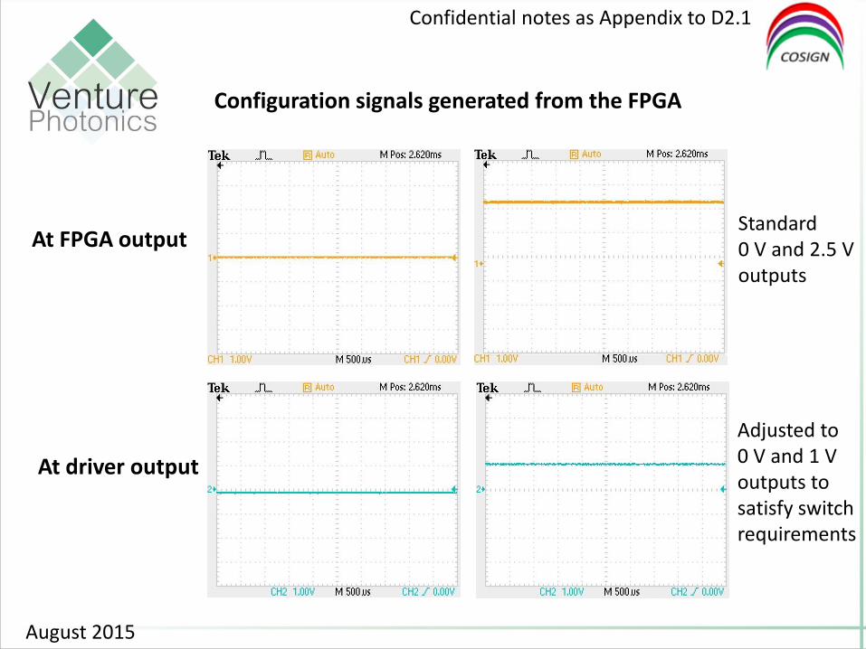
Configuration signals generated from the FPGA
At FPGA output
At driver output
Standard 0 V and 2.5 V outputs
Adjusted to 0 V and 1 V outputs to satisfy switch requirements
Confidential notes as Appendix to D2.1
August 2015
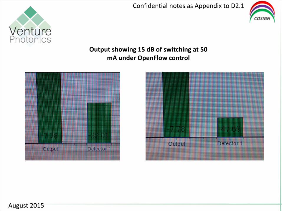
Output showing 15 dB of switching at 50 mA under OpenFlow control

Confidential notes as Appendix to D2.1
August 2015
In addition to the work required for D2.1 there has been substantial additional characterisation work undertaken. The next few pages show some of this data. This is not part of D2.1 but provides considerable additional confidence in the direction of development for the fast switch.

Confidential notes as Appendix to D2.1
August 2015
Additional testing of polarisation independence v wavelength
lensed fibre
chip
• Feedback-loop constant temperature control module is included in the test bed • Polarisation control method is proposed, verified and used to study the polarisation- independent switching performance • Computer-assisted sweeping measurement via GPIB is also established in the test bed.
Confidential notes as Appendix to D2.1
August 2015
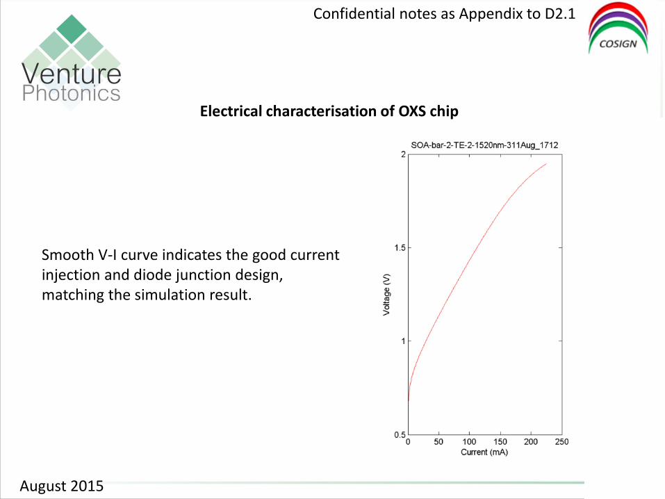
Smooth V-I curve indicates the good current injection and diode junction design, matching the simulation result.
Electrical characterisation of OXS chip
Confidential notes as Appendix to D2.1
August 2015
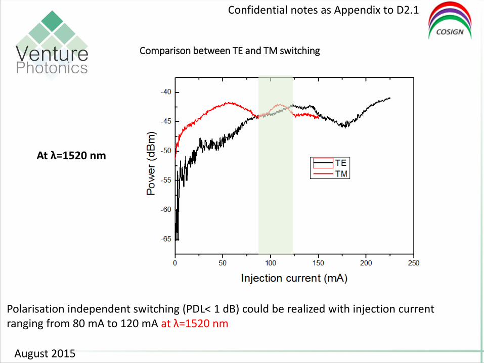
Comparison between TE and TM switching
At λ=1520 nm
Polarisation independent switching (PDL< 1 dB) could be realized with injection current ranging from 80 mA to 120 mA at λ=1520 nm
Confidential notes as Appendix to D2.1
August 2015
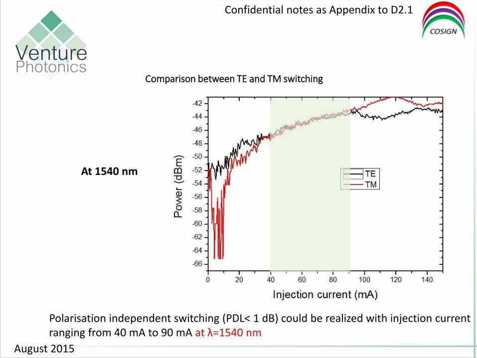
At 1540 nm
Polarisation independent switching (PDL< 1 dB) could be realized with injection current ranging from 40 mA to 90 mA at λ=1540 nm
Comparison between TE and TM switching
Confidential notes as Appendix to D2.1
August 2015
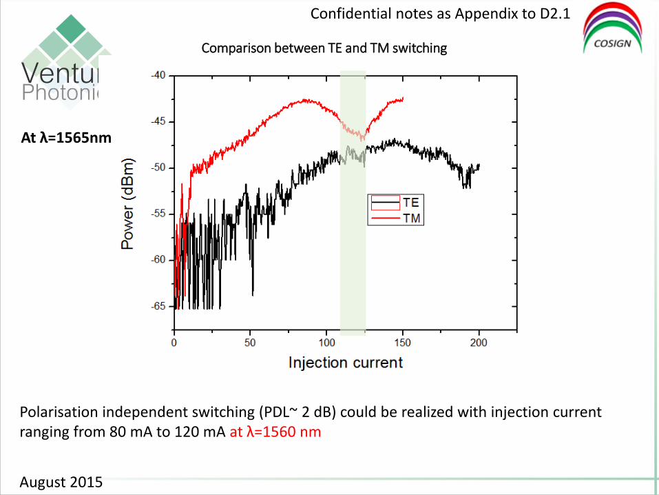
At λ=1565nm
Polarisation independent switching (PDL~ 2 dB) could be realized with injection current ranging from 80 mA to 120 mA at λ=1560 nm
Comparison between TE and TM switching

Confidential notes as Appendix to D2.1
August 2015
Conclusions
• D2.1 provides a summary of the demonstration that the integration of OpenFlow software with the driver circuit successfully controls the OXS. That report does not go into details of the chip and jigging issues addressed in order to provide that demonstration.
• This Appendix provides confidential technical background to that deliverable report.
• In addition the Appendix provides data to show that the electrical and optical results from the switch characterisation exhibit very encouraging optical performance metrics across the C-Band. These include polarisation independent switching to within a very few dB to better than 40 dB.
• Fast switching characterisation is planned to be demonstrated in the next few months with the completion of the follow-up wafer.
• After this there will be a substantial review of the data set before committing new materials into processing further development switches.


![COSIGN - European Commission : CORDIS · 619572 - ICT COSIGN [PUBLIC] D2.6 Combining Optics and SDN In next Generation data centre](https://img.dokumen.tips/doc/110x75/5b9a6e7e09d3f20b318b953f/cosign-european-commission-cordis-619572-ict-cosign-public-d26-combining.jpg)


![COSIGN - CORDIS€¦ · [2] COSIGN – Deliverable D1.3 – Comparative analysis of control plane alternatives 1.1.2 Acronyms and Abbreviations Most frequently usedacronyms in the](https://img.dokumen.tips/doc/110x75/5f050bed7e708231d410fe05/cosign-cordis-2-cosign-a-deliverable-d13-a-comparative-analysis-of-control.jpg)