Embed Size (px)
Citation preview
Grant Agreement No. 619572
COSIGN
Combining Optics and SDN In next Generation data centre Networks
Programme: Information and Communication Technologies Funding scheme: Collaborative Project – Large-Scale Integrating Project
Deliverable D2.4
Report on New Parallel Optics Transceiver Modules Based on 2.5D and 3D Integrated Components
Due date of deliverable: June 30, 2016 Actual submission date (Interim version): July 20, 2016
Actual submission date (Final version): December 21, 2016 Start date of project: January 1, 2014 Duration: 39 months Lead contractor for this deliverable: PhotonX Networks B.V.
COSIGN
Project co-funded by the European Commission within the Seventh Framework Programme Dissemination Level
PU Public X PP Restricted to other programme participants (including the Commission Services) RE Restricted to a group specified by the consortium (including the Commission Services) CO Confidential, only for members of the consortium (including the Commission Services)
Ref. Ares(2017)2261780 - 03/05/2017

619572 - ICT COSIGN [PUBLIC] D2.4 Combining Optics and SDN In next Generation data centre Networks
Page 2 of 20
Executive Summary This document describes the development effort by the Eindhoven University of Technology and PhotonX Networks B.V. to design, fabricate and test low cost, compact and simple to assemble parallel optics transceiver modules for use in future compact top of the rack data centre switches, which employ traditional electronic switches (L2/L3). In this task we focused on 3D and 2.5D stacking of ICs and different interposer materials using different techniques for processing the interposers.
Initially work was concentrated on a 3D stacked module. In Section 3.1 the main results coming from the 3D stacked parts are highlighted. Due to some of the fabrication aspects of the 3D stacking concept it was eventually decided to pursue a 2.5D stacking approach within COSIGN.
Using a silicon wafer as an interposer platform both a 2.5D transmitter and receiver module with 12 x10 Gbps operation and performance comparable to a commercial device has been demonstrated. The suggested interposer part can be directly flip-chipped on a PCB to be used as a mid-board optical engine or assembled on a secondary PCB and used as a pluggable module.
An alternative material to silicon and PCB was investigated for its feasibility in functioning as the interposer. The material, a photo-sensitive glass ceramic, can be processed in a similar fashion to silicon, but does not require the same complex infrastructure, such as a clean room, nor does it require the multi-layer processing that encompasses PCB, even though the material does offer multi-layering functionality.
The document has an accompanying, separate confidential appendix detailing a market assessment for the parallel optical transceivers that was undertaken by PhotonX Networks.
Legal Notice
The information in this document is subject to change without notice.
The Members of the COSIGN Consortium make no warranty of any kind with regard to this document, including, but not limited to, the implied warranties of merchantability and fitness for a particular purpose. The Members of the COSIGN Consortium shall not be held liable for errors contained herein or direct, indirect, special, incidental or consequential damages in connection with the furnishing, performance, or use of this material.
Possible inaccuracies of information are under the responsibility of the project. This report reflects solely the views of its authors. The European Commission is not liable for any use that may be made of the information contained therein.

619572 - ICT COSIGN [PUBLIC] D2.4 Combining Optics and SDN In next Generation data centre Networks
Page 3 of 20
Document Information
Status and Version: Final v2.0 Date of Issue: 21/12/2016 Dissemination level: Public Author(s): Name Partner Nathaniel Groothoff PHOTONX Oded Raz TUE Edited by: Nathaniel Groothoff PHOTONX Reviewed by: Tim Durrant VENTURE Michael Galili DTU Checked by: Sarah Ruepp DTU

619572 - ICT COSIGN [PUBLIC] D2.4 Combining Optics and SDN In next Generation data centre Networks
Page 4 of 20
Table of Contents Executive Summary .............................................................................................................................. 2
Table of Contents .................................................................................................................................. 4
1 Introduction ..................................................................................................................................... 5
1.1 Reference Material ..................................................................................................................... 5 1.1.1 Reference Documents ....................................................................................................... 5 1.1.2 Acronyms and Abbreviations ........................................................................................... 6
1.2 Document History ...................................................................................................................... 6
2 Progress and Trends in Parallel/Pluggable Optics Modules ....................................................... 7
3 3D Stacking of Optoelectronics on Top of CMOS ICs ................................................................ 9
3.1 Fabrication Process of 3D Stacked Transceiver ICs................................................................... 9
3.2 Scalability to Higher Bit Rates ................................................................................................. 10
3.3 3D Integration Complexity ....................................................................................................... 11
4 2.5D Stacking of Optoelectronics and CMOS ICs on a Silicon Interposer.............................. 12
4.1 Scheme of assembly and process steps ..................................................................................... 12
4.2 Testing experiments .................................................................................................................. 13
4.3 Developing a 3D stacking solution using the 2.5D stacking platform ..................................... 14 4.3.1 Concept of Assembly ...................................................................................................... 15 4.3.2 Thermal Modelling ......................................................................................................... 15 4.3.3 Interposer Fabrication Process ........................................................................................ 16
4.4 Initial work on a single mode VCSEL based 4x25 Gbps to Multi-Core fibre transmitter assembly ................................................................................................................................... 17
5 Optoelectronic Transceiver Using Alternative Material for the Interposer ............................ 18
6 Conclusions .................................................................................................................................... 20
619572 - ICT COSIGN [PUBLIC] D2.4 Combining Optics and SDN In next Generation data centre Networks
Page 5 of 20
1 Introduction Optical transceivers currently present the highest cost in terms of the bill of materials when building high end Ethernet switches with optical interfaces. Often the cost of optical transceivers is 5 to 8 times that of the cost of the ASIC+PCB board in which they are used [1]. Complementing the effort to build more compact Ethernet switches with densely integrated mid-board optical modules, a research effort towards compact, low cost and easy to assemble parallel optical modules has been included in the COSIGN project. In this document we summarize the main results of this effort executed by the COSIGN consortium, continuing the work reported in D2.2 “Report on 1st Generation TOR Switch Operation Based on 10 Gbps Base Rate Components”.
1.1 Reference Material
1.1.1 Reference Documents [1] Shimon Muller, “Mid board optics in Oracle switching solutions”, Symposium on Optical
Interconnects for Large-scale Datacenters and Supercomputers: Technologies, Packaging and Manufacturing, OFC 2016
[2] Avago, "MiniPOD and MicroPOD data sheet." [3] Finisar. CXP datasheet [Online]. Available:
http://www.finisar.com/sites/default/files/pdf/FTLD10CE1C%20Product%20Spec%20RevB2.pdf
[4] C. Schow, F. Doany, and J. Kash, "Get on the optical bus" Spectrum, IEEE, vol. 47, pp. 32-56 (2010)
[5] C. L. Schow, F. E. Doany, C. Chen, A. V. Rylyakov, C. W. Baks, D. M. Kuchta, R. A. John, and J. A. Kash, "Low-Power 16 x 10 Gb/s Bi-Directional Single Chip CMOS Optical Transceivers Operating at ≪ 5 mW/Gb/s/link" Solid-State Circuits, IEEE Journal of, vol. 44, pp. 301-313 (2009)
[6] A. Benner, "High-Bandwidth Integrated Optics for Server Applications", in proc. Of IEEE International Conference on Electrical Performance of Electronic Packaging and Systems, 2009
[7] King et al., "Commercial VCSELs and VCSEL arrays designed for FDR (14 Gbps) optical links", Proc. of SPIE Vol. 8276, 2012
[8] Guenter et al., "Reliability of VCSELs for >25Gb/s", OFC 2014, paper M3G.2 [9] Whittaker Report, "Industry Overview: Data Center Infrastructure", Blog post, February 29,
2016 (http://whittakerassociates.com/industry-overview-data-center-infrastructure/) [10] https://www.broadcom.com/collateral/pb/56840_PLUS-PB00-R.pdf [11] http://www.mellanox.com/page/products_dyn?product_family=175&mtag=tia [12] C. L. Schow, F. E. Doany, A. V. Rylyakov, B. G. Lee, C. V. Jahnes, Y. H. Kwark, C. W.
Baks, D. M. Kuchta, and J. A. Kash, "A 24-channel, 300 Gb/s, 8.2 pJ/bit, full-duplex fiber-coupled optical transceiver module based on a single “Holey” CMOS IC" Journal of Lightwave Technology, vol. 29, pp. 542-553 (2011)
[13] L. Dellmann, U. Drechsler, T. Morf, H. Rothuizen, R. Stutz, J. Weiss, and M. Despont, "3D opto-electrical device stacking on CMOS" Microelectronic Engineering, vol. 87, pp. 1210-1212 (2010)
[14] V. LECOCQ, "Hermetic packaging of a twelve-channel high bit rate VCSEL based transceiver" VCSEL day 2013
[15] A. G. Andreou, Z. K. Kalayjian, A. Apsel, P. Pouliquen, R. Athale, G. Simonis, and R. Reedy, "Silicon on sapphire CMOS for optoelectronic microsystems" Circuits and Systems Magazine, IEEE, vol. 1, pp. 22-30 (2001)
[16] Duan, P et al. "Demonstration of Wafer Scale Fabrication of 3-D Stacked Transmitter and Receiver Modules for Optical Interconnects." Journal of Lightwave Technology, vol. 31, no. 24, pp. 4073-4079 (2013)

619572 - ICT COSIGN [PUBLIC] D2.4 Combining Optics and SDN In next Generation data centre Networks
Page 6 of 20
[17] J. Rue et al, “High performance 10 Gb/s PIN and APD optical receivers”, proc. of Electronic Components and Technology, 1999
1.1.2 Acronyms and Abbreviations Most frequently used acronyms in the Deliverable are listed below. Additional acronyms may be specified and used throughout the text.
ASIC Application Specific Integrated Circuit BOM Bill of Materials CMOS Complementary Metal-Oxide Silicon CXP 100 Gbps (10x10 Gbps) pluggable optical module Datacomm Data communication Gbps Gigabits per second IC Integrated Circuit MBOM Mid-board Optical Module MOI Mechanical Optical Interface MPO Multi-fibre Push-On OE OptoElectronic PCB Printed Circuit Board PD Photodiode PR Photoresist PRBS Pseudo Random Bit Sequence PSGC Photo-Sensitive Glass Ceramic QSFP 40 Gbps (4x10 Gbps) pluggable optical module SEM Scanning Electron Microscope SerDes Serializer Deserializer TIA Transimpedance Amplifier TOR Top of Rack VCSEL Vertical-Cavity Surface-Emitting Laser
1.2 Document History Version Date Authors Comment V0.2 28/06/2016
See the list of authors
First draft for internal review V0.3 13/07/2016 Reviewer comments addressed V0.4 14/07/2016 Comments and suggestions by O. Raz V0.5 15/07/2016 Minor changes addressing comments V1.0 20/07/2016 Formatting and consistency check. This was
the version submitted as the Interim Version. V1.1 5/12/2016 Updated with new information from O. Raz
and N. Groothoff V1.2 13/12/2016 Moved appendix to separate document.
Internal review version. V1.3 16/12/2016 M. Galili comments addressed V1.4 20/12/2016 T. Durrant comments addressed V2.0 21/12/2016 Quality Check – Final version
619572 - ICT COSIGN [PUBLIC] D2.4 Combining Optics and SDN In next Generation data centre Networks
Page 7 of 20
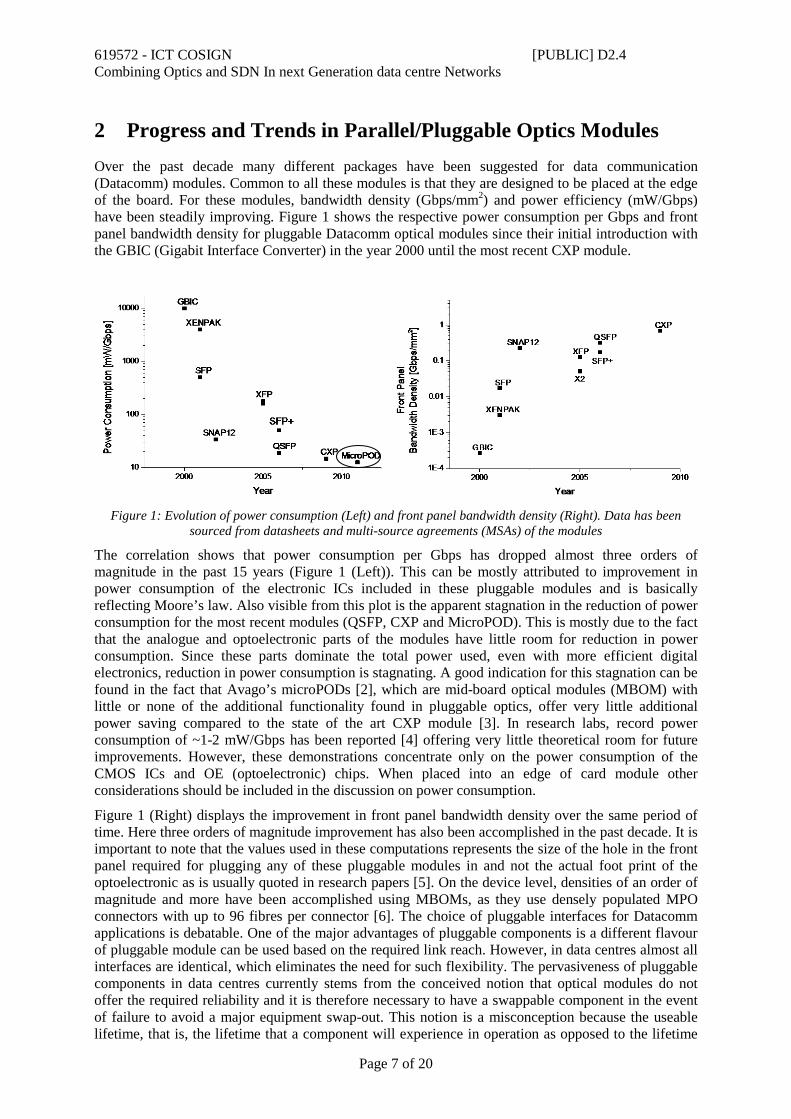
2 Progress and Trends in Parallel/Pluggable Optics Modules Over the past decade many different packages have been suggested for data communication (Datacomm) modules. Common to all these modules is that they are designed to be placed at the edge of the board. For these modules, bandwidth density (Gbps/mm2) and power efficiency (mW/Gbps) have been steadily improving. Figure 1 shows the respective power consumption per Gbps and front panel bandwidth density for pluggable Datacomm optical modules since their initial introduction with the GBIC (Gigabit Interface Converter) in the year 2000 until the most recent CXP module.
Figure 1: Evolution of power consumption (Left) and front panel bandwidth density (Right). Data has been
sourced from datasheets and multi-source agreements (MSAs) of the modules
The correlation shows that power consumption per Gbps has dropped almost three orders of magnitude in the past 15 years (Figure 1 (Left)). This can be mostly attributed to improvement in power consumption of the electronic ICs included in these pluggable modules and is basically reflecting Moore’s law. Also visible from this plot is the apparent stagnation in the reduction of power consumption for the most recent modules (QSFP, CXP and MicroPOD). This is mostly due to the fact that the analogue and optoelectronic parts of the modules have little room for reduction in power consumption. Since these parts dominate the total power used, even with more efficient digital electronics, reduction in power consumption is stagnating. A good indication for this stagnation can be found in the fact that Avago’s microPODs [2], which are mid-board optical modules (MBOM) with little or none of the additional functionality found in pluggable optics, offer very little additional power saving compared to the state of the art CXP module [3]. In research labs, record power consumption of ~1-2 mW/Gbps has been reported [4] offering very little theoretical room for future improvements. However, these demonstrations concentrate only on the power consumption of the CMOS ICs and OE (optoelectronic) chips. When placed into an edge of card module other considerations should be included in the discussion on power consumption.
Figure 1 (Right) displays the improvement in front panel bandwidth density over the same period of time. Here three orders of magnitude improvement has also been accomplished in the past decade. It is important to note that the values used in these computations represents the size of the hole in the front panel required for plugging any of these pluggable modules in and not the actual foot print of the optoelectronic as is usually quoted in research papers [5]. On the device level, densities of an order of magnitude and more have been accomplished using MBOMs, as they use densely populated MPO connectors with up to 96 fibres per connector [6]. The choice of pluggable interfaces for Datacomm applications is debatable. One of the major advantages of pluggable components is a different flavour of pluggable module can be used based on the required link reach. However, in data centres almost all interfaces are identical, which eliminates the need for such flexibility. The pervasiveness of pluggable components in data centres currently stems from the conceived notion that optical modules do not offer the required reliability and it is therefore necessary to have a swappable component in the event of failure to avoid a major equipment swap-out. This notion is a misconception because the useable lifetime, that is, the lifetime that a component will experience in operation as opposed to the lifetime

619572 - ICT COSIGN [PUBLIC] D2.4 Combining Optics and SDN In next Generation data centre Networks
Page 8 of 20
before failure, is shorter than the lifetime before failure often leading to the component being exchanged for a newer model before failure. For example, VCSELs' mean time to failure are now approaching > 50 years [7]], [[8] and the average data center life span, although widely varying, is on the order of 10 years [9].
The use of MBOMs may offer substantial power savings when the entire system is considered. MBOMs can be placed much closer to switching ICs and can therefore allow for significant energy saving in the input and output stages of the SerDes's, which are now embedded in the switching ICs [10]. On the other side of this link, power savings can also be gained in the optical modules, as most ICs designed for parallel optic interconnects support re-configuration of output and input power levels [11]. By moving towards MBOM solutions, the front panel bandwidth density can be dramatically increased solving a major bottleneck in the design of data centre switches. The major challenge is therefore to improve the reliability of photonic components, or to build redundancy into these systems to minimize the impact of component failure and untimely maintenance.
619572 - ICT COSIGN [PUBLIC] D2.4 Combining Optics and SDN In next Generation data centre Networks
Page 9 of 20
3 3D Stacking of Optoelectronics on Top of CMOS ICs Several projects and groups have explored the stacking of optoelectronics on CMOS for achieving the most compact solution for parallel interconnects [12],[13],[14],[15]. While these efforts focused on achieving the desirable functionality, they were often based on costly and complicated procedures. It is clear that the most compact way of integrating the CMOS and OE dies is to stack them up in 3D. The sections below provide more details concerning the 3D stacking technique developed by TUE.
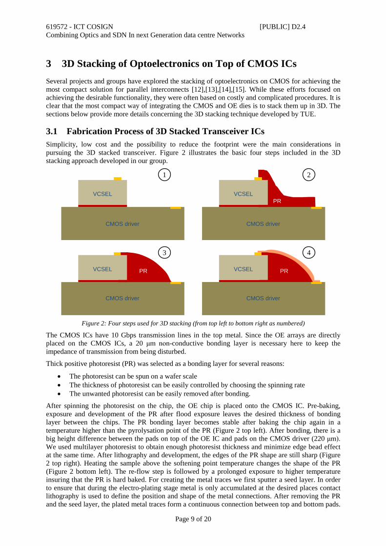
3.1 Fabrication Process of 3D Stacked Transceiver ICs Simplicity, low cost and the possibility to reduce the footprint were the main considerations in pursuing the 3D stacked transceiver. Figure 2 illustrates the basic four steps included in the 3D stacking approach developed in our group.
Figure 2: Four steps used for 3D stacking (from top left to bottom right as numbered)
The CMOS ICs have 10 Gbps transmission lines in the top metal. Since the OE arrays are directly placed on the CMOS ICs, a 20 μm non-conductive bonding layer is necessary here to keep the impedance of transmission from being disturbed.
Thick positive photoresist (PR) was selected as a bonding layer for several reasons:
• The photoresist can be spun on a wafer scale • The thickness of photoresist can be easily controlled by choosing the spinning rate • The unwanted photoresist can be easily removed after bonding.
After spinning the photoresist on the chip, the OE chip is placed onto the CMOS IC. Pre-baking, exposure and development of the PR after flood exposure leaves the desired thickness of bonding layer between the chips. The PR bonding layer becomes stable after baking the chip again in a temperature higher than the pyrolysation point of the PR (Figure 2 top left). After bonding, there is a big height difference between the pads on top of the OE IC and pads on the CMOS driver (220 μm). We used multilayer photoresist to obtain enough photoresist thickness and minimize edge bead effect at the same time. After lithography and development, the edges of the PR shape are still sharp (Figure 2 top right). Heating the sample above the softening point temperature changes the shape of the PR (Figure 2 bottom left). The re-flow step is followed by a prolonged exposure to higher temperature insuring that the PR is hard baked. For creating the metal traces we first sputter a seed layer. In order to ensure that during the electro-plating stage metal is only accumulated at the desired places contact lithography is used to define the position and shape of the metal connections. After removing the PR and the seed layer, the plated metal traces form a continuous connection between top and bottom pads.
CMOS driver
VCSEL
PR
CMOS driver
VCSEL
PR
CMOS driver
VCSEL
PR
CMOS driver
VCSEL
2 1
4 3
619572 - ICT COSIGN [PUBLIC] D2.4 Combining Optics and SDN In next Generation data centre Networks
Page 10 of 20
The metal path shapes are defined by a lithography mask, and the thickness of the metal paths is controlled by the plating process (Figure 2 bottom right).
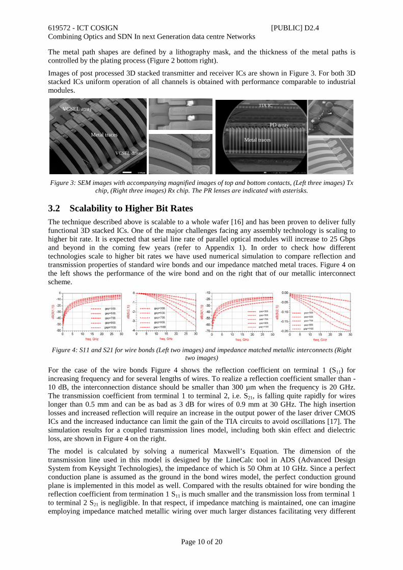
Images of post processed 3D stacked transmitter and receiver ICs are shown in Figure 3. For both 3D stacked ICs uniform operation of all channels is obtained with performance comparable to industrial modules.
Figure 3: SEM images with accompanying magnified images of top and bottom contacts, (Left three images) Tx
chip, (Right three images) Rx chip. The PR lenses are indicated with asterisks.
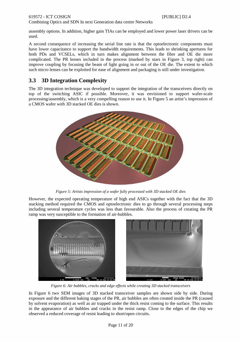
3.2 Scalability to Higher Bit Rates The technique described above is scalable to a whole wafer [16] and has been proven to deliver fully functional 3D stacked ICs. One of the major challenges facing any assembly technology is scaling to higher bit rate. It is expected that serial line rate of parallel optical modules will increase to 25 Gbps and beyond in the coming few years (refer to Appendix 1). In order to check how different technologies scale to higher bit rates we have used numerical simulation to compare reflection and transmission properties of standard wire bonds and our impedance matched metal traces. Figure 4 on the left shows the performance of the wire bond and on the right that of our metallic interconnect scheme.
Figure 4: S11 and S21 for wire bonds (Left two images) and impedance matched metallic interconnects (Right
two images)
For the case of the wire bonds Figure 4 shows the reflection coefficient on terminal 1 (S11) for increasing frequency and for several lengths of wires. To realize a reflection coefficient smaller than -10 dB, the interconnection distance should be smaller than 300 µm when the frequency is 20 GHz. The transmission coefficient from terminal 1 to terminal 2, i.e. S21, is falling quite rapidly for wires longer than 0.5 mm and can be as bad as 3 dB for wires of 0.9 mm at 30 GHz. The high insertion losses and increased reflection will require an increase in the output power of the laser driver CMOS ICs and the increased inductance can limit the gain of the TIA circuits to avoid oscillations [17]. The simulation results for a coupled transmission lines model, including both skin effect and dielectric loss, are shown in Figure 4 on the right.
The model is calculated by solving a numerical Maxwell’s Equation. The dimension of the transmission line used in this model is designed by the LineCalc tool in ADS (Advanced Design System from Keysight Technologies), the impedance of which is 50 Ohm at 10 GHz. Since a perfect conduction plane is assumed as the ground in the bond wires model, the perfect conduction ground plane is implemented in this model as well. Compared with the results obtained for wire bonding the reflection coefficient from termination 1 S11 is much smaller and the transmission loss from terminal 1 to terminal 2 S21 is negligible. In that respect, if impedance matching is maintained, one can imagine employing impedance matched metallic wiring over much larger distances facilitating very different
VCSEL array
Metal traces
VCSEL driver
Metal traces
TIA IC
PD array
*
*
619572 - ICT COSIGN [PUBLIC] D2.4 Combining Optics and SDN In next Generation data centre Networks
Page 11 of 20
assembly options. In addition, higher gain TIAs can be employed and lower power laser drivers can be used.
A second consequence of increasing the serial line rate is that the optoelectronic components must have lower capacitance to support the bandwidth requirements. This leads to shrinking apertures for both PDs and VCSELs, which in turn makes alignment between the fibre and OE die more complicated. The PR lenses included in the process (marked by stars in Figure 3, top right) can improve coupling by focusing the beam of light going in or out of the OE die. The extent to which such micro lenses can be exploited for ease of alignment and packaging is still under investigation.
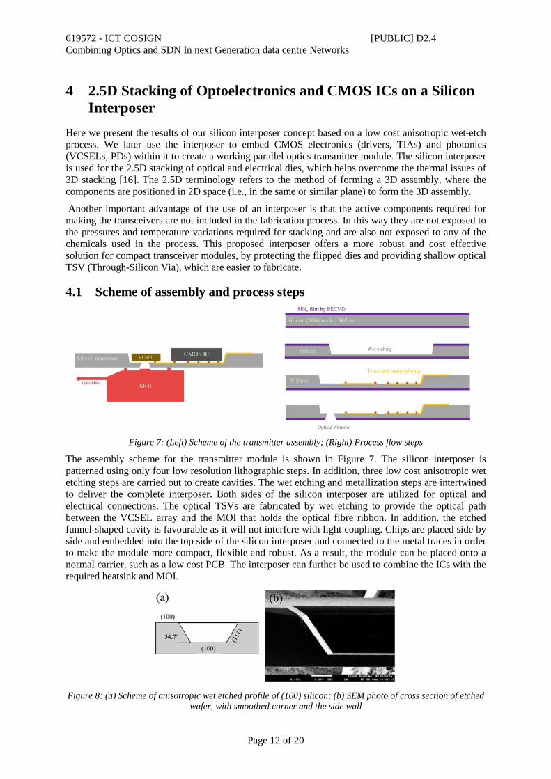
3.3 3D Integration Complexity The 3D integration technique was developed to support the integration of the transceivers directly on top of the switching ASIC if possible. Moreover, it was envisioned to support wafer-scale processing/assembly, which is a very compelling reason to use it. In Figure 5 an artist’s impression of a CMOS wafer with 3D stacked OE dies is shown.
Figure 5: Artists impression of a wafer fully processed with 3D stacked OE dies
However, the expected operating temperature of high end ASICs together with the fact that the 3D stacking method required the CMOS and optoelectronic dies to go through several processing steps including several temperature cycles was less than favourable. Also the process of creating the PR ramp was very susceptible to the formation of air-bubbles.
Figure 6: Air bubbles, cracks and edge effects while creating 3D stacked transceivers
In Figure 6 two SEM images of 3D stacked transceiver samples are shown side by side. During exposure and the different baking stages of the PR, air bubbles are often created inside the PR (caused by solvent evaporation) as well as air trapped under the thick resist coming to the surface. This results in the appearance of air bubbles and cracks in the resist ramp. Close to the edges of the chip we observed a reduced coverage of resist leading to short/open circuits.
619572 - ICT COSIGN [PUBLIC] D2.4 Combining Optics and SDN In next Generation data centre Networks
Page 12 of 20
4 2.5D Stacking of Optoelectronics and CMOS ICs on a Silicon Interposer
Here we present the results of our silicon interposer concept based on a low cost anisotropic wet-etch process. We later use the interposer to embed CMOS electronics (drivers, TIAs) and photonics (VCSELs, PDs) within it to create a working parallel optics transmitter module. The silicon interposer is used for the 2.5D stacking of optical and electrical dies, which helps overcome the thermal issues of 3D stacking [16]. The 2.5D terminology refers to the method of forming a 3D assembly, where the components are positioned in 2D space (i.e., in the same or similar plane) to form the 3D assembly.
Another important advantage of the use of an interposer is that the active components required for making the transceivers are not included in the fabrication process. In this way they are not exposed to the pressures and temperature variations required for stacking and are also not exposed to any of the chemicals used in the process. This proposed interposer offers a more robust and cost effective solution for compact transceiver modules, by protecting the flipped dies and providing shallow optical TSV (Through-Silicon Via), which are easier to fabricate.
4.1 Scheme of assembly and process steps
Figure 7: (Left) Scheme of the transmitter assembly; (Right) Process flow steps
The assembly scheme for the transmitter module is shown in Figure 7. The silicon interposer is patterned using only four low resolution lithographic steps. In addition, three low cost anisotropic wet etching steps are carried out to create cavities. The wet etching and metallization steps are intertwined to deliver the complete interposer. Both sides of the silicon interposer are utilized for optical and electrical connections. The optical TSVs are fabricated by wet etching to provide the optical path between the VCSEL array and the MOI that holds the optical fibre ribbon. In addition, the etched funnel-shaped cavity is favourable as it will not interfere with light coupling. Chips are placed side by side and embedded into the top side of the silicon interposer and connected to the metal traces in order to make the module more compact, flexible and robust. As a result, the module can be placed onto a normal carrier, such as a low cost PCB. The interposer can further be used to combine the ICs with the required heatsink and MOI.
Figure 8: (a) Scheme of anisotropic wet etched profile of (100) silicon; (b) SEM photo of cross section of etched
wafer, with smoothed corner and the side wall

619572 - ICT COSIGN [PUBLIC] D2.4 Combining Optics and SDN In next Generation data centre Networks
Page 13 of 20
The main challenge in using the silicon wafer as an interposer is to create the recesses in the silicon for the embedding of the dies and the required optical via to allow light in and out coupling for the flip-chipped components. Figure 8 shows a cross section of such an etched recess following a two-step wet etching process. While the actual creation of a recess through the use of wet etching will deliver the desired depth, the need to metalize the slopes forces a 2nd etching step to smooth the edges of the obtained recess.
Once all the processing steps are complete, and depending on the size of the processed wafer, we can get multiple interposers on a single wafer produced at the same time. Figure 9 shows a couple of SEM images of the interposers with metalized traces along with a completed wafer with a number of interposers on it.
Figure 9: (a) SEM photo of 12 × 10G transmitter silicon interposer, (b) 4 × 25G transceiver, and (c) photo of
processed diced 1-inch wafer, containing two types of silicon interposers
The fully assembled transmitter module is shown in Figure 10. Once the dies have been bonded, a MOI and PRIZM LightTurn (both from US CONEC) are placed on the back of the interposer with the flip-chip machine (using visual alignment). The fibre array is then attached on top to allow in/out coupling to an MPO 12-fibre connector.
Figure 10: Photo of complete transmitter, contain the assembled silicon interposer (inverted), MOI and
PRIZM® LightTurn®
4.2 Testing experiments It is important to verify the data integrity of the transceiver, which is done by performing testing using the scheme shown in Figure 11. The microcontroller is connected to the control pads of the IC from a driver circuit via DC probes, and the driver is driven with 3.3 V power supply. The register of the driver can be read and written to using a Labview program. The emitted optical signals are coupled out of the transceiver through the PRIZM LightTurn and MOI and connected to an oscilloscope via the SFP+ form factor connectors to record eye diagrams.
(c)
5mm

619572 - ICT COSIGN [PUBLIC] D2.4 Combining Optics and SDN In next Generation data centre Networks
Page 14 of 20
Figure 11: Scheme of test set up of assembled silicon interposer
The 12.5 Gbps differential signal, with PRBS 231-1 sequence, is fed into the fan out pads on the interposer through an RF probe channel by channel. The multimode 850 nm optical input/output to/from the PD/VCSEL array is connected to a commercial SFP+ module used as a high speed multimode transmitter/photo detector. Figure 12 shows the eye diagrams of all the Datacomm ports, both Tx and Rx channels and good eye openings are observed for all channels. Due to a short circuit on the interposer, Ch. 8 on the VCSEL transmitter was not working. Performance of the transceiver with silicon interposer is comparable to that of the commercial SFP+ module which is used as a back to back (B2B) reference.
Figure 12: (Left) Eye patterns of 11 enabled VCSEL channels and back to back test at 12.5 Gbps, (Right) Eye
patterns of 12 enabled PD channels
4.3 Developing a 3D stacking solution using the 2.5D stacking platform The integration platform suggested in Section 4.1 can be adapted to create an even more compact solution, which will see the two dies placed vertically on top of each other but will not be directly stacked. In the following sections we will describe preliminary work carried out in the TU/e for supporting 3D like stacking using a 2.5D stacking platform.
619572 - ICT COSIGN [PUBLIC] D2.4 Combining Optics and SDN In next Generation data centre Networks
Page 15 of 20
4.3.1 Concept of Assembly The pads on CMOS IC are located at the perimeter of the chip area for further connection and packaging, and we propose to use the central area for opto-electronic die assembly. The package of transmitter/receiver module scheme is shown in Figure 13 (left), where both front and back sides of the silicon interposer are utilized for electrical and optical connection, respectively. The optical die fits in the wet etched cavity, and the depth of the cavity can be controlled by etching time. Therefore, the air gap between CMOS IC and optical die is formed after embedding. The pads on the CMOS chip are routed and redistributed on the surface of the silicon interposer, and the 125 μm pads on the dies are fanned out to a 250 μm pitch. The optical through silicon vias, for each channel, are vertically formed by double-side etching of silicon. Then, the mechanical optical interface (MOI) is fixed at the back side, and the PRIZM® LightTurn® System is utilized for light coupling into a standard fibre array. The footprint of this 10 Gbps 12-channel transmitter and receiver module will be reduced to 4 mm × 6 mm.
Figure 13: (left) scheme of 3D assembly of CMOS driver, VCSEL, silicon interposer and MOI; (right) process
step of silicon interposer: (a) SiNx deposition; (b) KOH etching; (c) lithography on etched topology; (d) electro-plating traces and solder bumps; (e) wet etching on both sides.
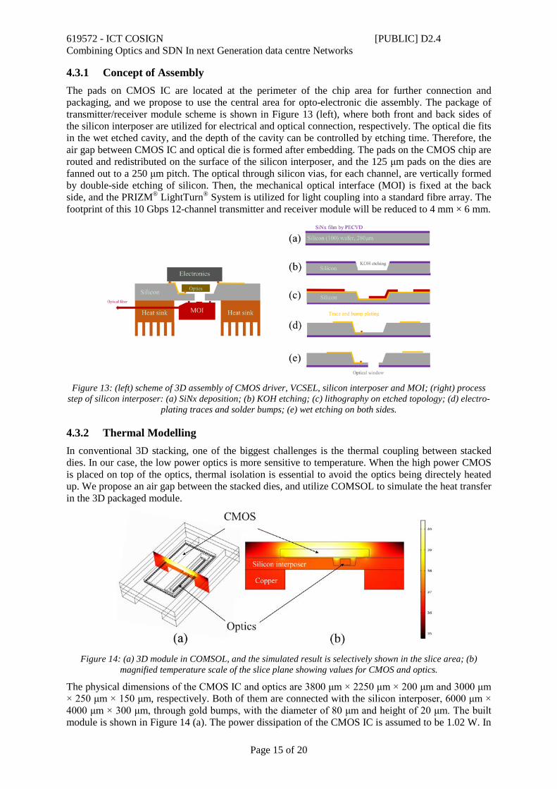
4.3.2 Thermal Modelling In conventional 3D stacking, one of the biggest challenges is the thermal coupling between stacked dies. In our case, the low power optics is more sensitive to temperature. When the high power CMOS is placed on top of the optics, thermal isolation is essential to avoid the optics being directely heated up. We propose an air gap between the stacked dies, and utilize COMSOL to simulate the heat transfer in the 3D packaged module.
Figure 14: (a) 3D module in COMSOL, and the simulated result is selectively shown in the slice area; (b)
magnified temperature scale of the slice plane showing values for CMOS and optics.
The physical dimensions of the CMOS IC and optics are 3800 μm × 2250 μm × 200 μm and 3000 μm × 250 μm × 150 μm, respectively. Both of them are connected with the silicon interposer, 6000 μm × 4000 μm × 300 μm, through gold bumps, with the diameter of 80 μm and height of 20 μm. The built module is shown in Figure 14 (a). The power dissipation of the CMOS IC is assumed to be 1.02 W. In
619572 - ICT COSIGN [PUBLIC] D2.4 Combining Optics and SDN In next Generation data centre Networks
Page 16 of 20
the scheme, the heatsink will be connected on the back side of the CMOS IC, so two blocks of copper, 6000 μm × 1000 μm × 500 μm, are attached to the interposer. We treat the opposite side of copper as a convective boundary, with the heat transfer coefficient (HTC) of 5000 W/K·m2. The CMOS is situated in ambient air and has a thickness of 400 μm. The HTC of other boundries is set to 5 W/K·m2, nearly adiabatic.
We assume the initial temperature to be 22 ℃, and the solver runs the calculation until the system is in thermal equilibrium. The simulation result is shown in Figure 14 (b). The highest temperature is 40.4 ℃ on the CMOS IC. In addition, the temperature of the optics stays at 37.1 ℃, 3.3 ℃ below the CMOS. We also simulate the same module under the same conditions but with no air gap and find that the optics stay the same temperature as the CMOS IC. Due to the air gap between the optical die and CMOS chip, the heat cannot directly transfer to the optics. The thin layer of air is a very good isolation to avoid thermal crosstalk. Thus, the proposed 3D scheme exhibits a thermal advatange over conventional 3D stacking approach.
4.3.3 Interposer Fabrication Process The silicon interposer is fabricated on a wafer level. The patterning process includes 5 steps of lithography, and the process flow is shown in Figure 13 (right).
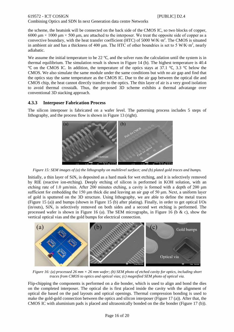
Figure 15: SEM images of (a) the lithography on multilevel surface; and (b) plated gold traces and bumps.
Initially, a thin layer of SiNx is deposited as a hard mask for wet etching, and it is selectively removed by RIE (reactive ion-etching). Deeply etching of silicon is performed in KOH solution, with an etching rate of 1.0 μm/min. After 200 minutes etching, a cavity is formed with a depth of 200 μm sufficient for embedding the 150 μm thick die and leaving an air gap of 50 μm. Next, a uniform layer of gold is sputtered on the 3D structure. Using lithography, we are able to define the metal traces (Figure 15 (a)) and bumps (shown in Figure 15 (b) after plating). Finally, in order to get optical I/Os (in/outs), SiNx is selectively removed on both sides and a second wet etching is performed. The processed wafer is shown in Figure 16 (a). The SEM micrographs, in Figure 16 (b & c), show the vertical optical vias and the gold bumps for electrical connection.
Figure 16: (a) processed 26 mm × 26 mm wafer; (b) SEM photo of etched cavity for optics, including short
traces from CMOS to optics and optical vias; (c) magnified SEM photo of optical via.
Flip-chipping the components is performed on a die bonder, which is used to align and bond the dies on the completed interposer. The optical die is first placed inside the cavity with the alignment of optical die based on the pad layouts and optical openings. Thermal compression bonding is used to make the gold-gold connection between the optics and silicon interposer (Figure 17 (a)). After that, the CMOS IC with aluminium pads is placed and ultrasonically bonded on the die bonder (Figure 17 (b)).
619572 - ICT COSIGN [PUBLIC] D2.4 Combining Optics and SDN In next Generation data centre Networks
Page 17 of 20
Finally, the MOI is passively aligned with etched optical vias on the other side with the same tool and fixed by epoxy.
Figure 17: SEM photography of (a) VCSEL array embedded inside cavity, and (b) CMOS chip on same
interposer covering the VCSEL array to create a 3D assembly.
4.4 Initial work on a single mode VCSEL based 4x25 Gbps to Multi-Core fibre transmitter assembly
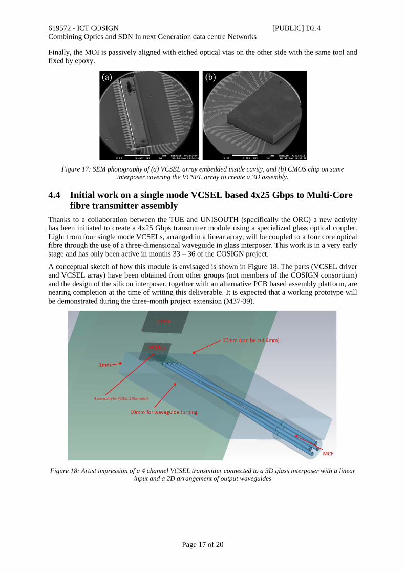
Thanks to a collaboration between the TUE and UNISOUTH (specifically the ORC) a new activity has been initiated to create a 4x25 Gbps transmitter module using a specialized glass optical coupler. Light from four single mode VCSELs, arranged in a linear array, will be coupled to a four core optical fibre through the use of a three-dimensional waveguide in glass interposer. This work is in a very early stage and has only been active in months 33 – 36 of the COSIGN project.
A conceptual sketch of how this module is envisaged is shown in Figure 18. The parts (VCSEL driver and VCSEL array) have been obtained from other groups (not members of the COSIGN consortium) and the design of the silicon interposer, together with an alternative PCB based assembly platform, are nearing completion at the time of writing this deliverable. It is expected that a working prototype will be demonstrated during the three-month project extension (M37-39).
Figure 18: Artist impression of a 4 channel VCSEL transmitter connected to a 3D glass interposer with a linear
input and a 2D arrangement of output waveguides
619572 - ICT COSIGN [PUBLIC] D2.4 Combining Optics and SDN In next Generation data centre Networks
Page 18 of 20
5 Optoelectronic Transceiver Using Alternative Material for the Interposer
With the aim to develop compact, low cost and easy to assemble parallel optical modules, the material choice for the interposer can impact on the overall BOM and assembly simplicity. For silicon processing it is generally required to use clean room technology. Although Section 4 reports the use of low resolution lithographic and low cost anisotropic wet etching to process the silicon, it is still required to conduct these processing steps in a clean room environment. This adds additional cost and complexity to the fabrication process even though this process is well developed. In this Section we explore a prototype transceiver to examine the feasibility for an alternative material, a photo-sensitive glass ceramic (PSGC), which can be processed more easily than silicon but still enables the ability to machine the material with cavities, open recesses and multi-layering of the PSGC.
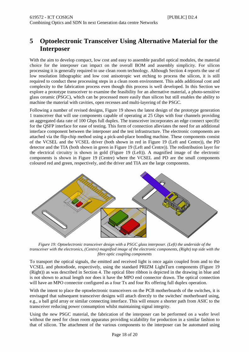
Following a number of revised designs, Figure 19 shows the latest design of the prototype generation 1 transceiver that will use components capable of operating at 25 Gbps with four channels providing an aggregated data rate of 100 Gbps full duplex. The transceiver incorporates an edge connect specific for the QSFP interface for ease of testing. This form of connection alleviates the need for an additional interface component between the interposer and the test infrastructure. The electronic components are attached via the flip-chip method using a pick-and-place bonding machine. These components consist of the VCSEL and the VCSEL driver (both shown in red in Figure 19 (Left and Centre)), the PD detector and the TIA (both shown in green in Figure 19 (Left and Centre)). The redistribution layer for the electrical circuitry is shown in gold (Figure 19 (Left)). A magnified image of the electronic components is shown in Figure 19 (Centre) where the VCSEL and PD are the small components coloured red and green, respectively, and the driver and TIA are the large components.
Figure 19: Optoelectronic transceiver design with a PSGC glass interposer. (Left) the underside of the
transceiver with the electronics, (Centre) magnified image of the electronic components, (Right) top side with the fibre optic coupling components
To transport the optical signals, the emitted and received light is once again coupled from and to the VCSEL and photodiode, respectively, using the standard PRIZM LightTurn components (Figure 19 (Right)) as was described in Section 4. The optical fibre ribbon is depicted in the drawing in blue and is not shown to actual length nor does it have the MPO end connector drawn. The optical connection will have an MPO connector configured as a four Tx and four Rx offering full duplex operation.
With the intent to place the optoelectronic transceivers on the PCB motherboards of the switches, it is envisaged that subsequent transceiver designs will attach directly to the switches' motherboard using, e.g., a ball grid array or similar connecting interface. This will ensure a shorter path from ASIC to the transceiver reducing power consumption whilst maintaining signal integrity.
Using the new PSGC material, the fabrication of the interposer can be performed on a wafer level without the need for clean room apparatus providing scalability for production in a similar fashion to that of silicon. The attachment of the various components to the interposer can be automated using

619572 - ICT COSIGN [PUBLIC] D2.4 Combining Optics and SDN In next Generation data centre Networks
Page 19 of 20
flip-chip and pick-and-place machinery to also provide the necessary level of automation for high volume cost considerations. In addition, this material in combination with a specialized bonding process offers the capability of being bonded to a variety of materials without needing specific adhesives or elevated temperatures. This offers a great deal of flexibility with the material and would allow for a variety of design considerations depending on the intended interposer requirements.
The prototype generation 1 transceiver had not been produced at the time of submitting the interim deliverable dated 20th June 2016. A number of issues arose causing delays to the development of the interposer and subsequent transceiver. These issues included a prolonged response from the electronic component suppliers in providing the necessary datasheets needed for the appropriate design of the transceiver and ongoing discussions with the fabricator of the interposer on the most suitable design to comply with their capabilities and remain within the budget allocated for the fabrication.
Thermal considerations for the ICs are important to understand what cooling mechanisms are necessary to ensure the ICs operate appropriately. The thermal load on the PSGC interposer based transceiver was assessed using the MARC-Mentat simulation software from MSC Software. The thermal load during operation was taken from the specification sheets of the various components. The simulation time-frame was a duration of 300 seconds ensuring that the thermal condition had stabilised and a forced air flow creating an atmospheric thermal conductivity of 50 W/m/K. The transceiver was simulated with and without a heatsink (Figure 20 (left)) and for a silicon interposer for comparison. Figure 20 (right) shows the resulting temperatures of the different components. It is evident that the heat sink is necessary to ensure that the components operate under their maximum operating temperature (around 95°C). For comparative purposes, the PSGC was substituted with silicon to examine the difference in interposer thermal conductivity. It is also evident from the lower thermal conductivity of glass that the components maintain a higher temperature and the heatsink is necessary for proper functioning.
Figure 20: Optoelectronic transceiver design with heatsink (left) and effect of material and heatsink on
component temperature using glass or silicon interposer for the same atmospheric convection (50 W/m/K) (right).
A decision on whether to proceed with the fabrication of this prototype is still pending. The price for the fabrication was higher than anticipated and as such, careful consideration as to the viability of the outcomes of this prototype needs to be evaluated. The price of fabrication included non-recurring engineering costs that add considerable overhead to fabrication efforts. With a focus on MBOMs to be integrated into Ethernet switches, the current prototype design does not conform to a suitable form factor that would satisfy this requirement. If fabricating the prototype does not represent the best means to establish the feasibility of the fabrication methods, then a different design would be a more appropriate direction to pursue. The processing of the PSGC material is currently offered by a single company and therefore alternative sources of fabrication were not available. At present, this is a negative aspect for using this technology. A new transceiver design is being considered that would better complement the ideals of the project.
619572 - ICT COSIGN [PUBLIC] D2.4 Combining Optics and SDN In next Generation data centre Networks
Page 20 of 20
6 Conclusions The need for low cost, compact and easy to assemble/package parallel optical interconnects was the main driver behind all the activities described in this document. The development of mid-board optical modules supports the goal of the project to offer optics-based functionality of future data centre fabric. Several parallel approaches have been investigated to offer solutions and devices to cater for the future data centre infrastructure.
Initial work was carried out on 3D stacking of CMOS and OE dies. While this approach delivered working prototypes, it suffered from several drawbacks such as a susceptibility to air bubble creation and cracks, and challenging thermal conditions for the OE dies. To solve these problems two alternate approaches were investigated based on 2.5D stacking where an interposer is used as a carrier for the ICs and the required optics (for light coupling). Using standard 100 silicon wafers and a simple wet etching process, we have demonstrated working 12x10 Gbps transmitter and receiver modules at the 850 nm wavelength window with multi-mode fibres. Performance of the modules was comparable to that of commercial parallel optics modules.
The design of the interposer with PSGC material has been completed and negotiations for fabrication are ongoing. The prototype generation 1 optoelectronic transceiver will provide important information for the generation 2 transceiver that is envisaged to be placed directly on the PCB motherboard of the switch and as close as possible to the ASIC. A thermal simulation to determine the required cooling of the transceiver was performed. The outcome was that forced air cooling and a thermal heatsink would be required to maintain the components below the maximum operating temperatures.
All activities reported in this deliverable have the objective of achieving improved and redesigned hardware to meet the ever increasing demands of data centre networks. This involves shrinking the size of the switches by using MBOMs, which also offers higher front port density and thereby increased bandwidth. The OE transceivers were developed with the aim to offer a more compact, low cost and easy to assemble parallel optical module to satisfy the power consumption reductions and optical port increases. The transceiver designs covered a number of different options: including stacking the CMOS and IC components forming a 3D structure; structuring the interposer to incorporate the components forming a 2.5D fabrication technique; and choosing the material of the interposer to address some of the disadvantages of using silicon as an interposer.


![COSIGN - CORDIS · 619572 - ICT COSIGN [PUBLIC] D2.5 Combining Optics and SDN In next Generation data centre Networks Page 7 of 15 2 Second Generation Multi-Core Fibres Suitable for](https://img.dokumen.tips/doc/110x75/5ed2f3d13e92a05e0d15d5a6/cosign-cordis-619572-ict-cosign-public-d25-combining-optics-and-sdn-in-next.jpg)


![Audio R-sta s cs · Blogging about R Audio recording of this talk is on: R-sta s cs.com Tal Galili[1] [1] Department of Statistics and Operations Research, Tel Aviv University, Israel](https://img.dokumen.tips/doc/110x75/5f04bb957e708231d40f6e63/audio-r-sta-s-cs-blogging-about-r-audio-recording-of-this-talk-is-on-r-sta-s-cscom.jpg)
![COSIGN - CORDIS · 2017. 5. 24. · 619572 - ICT COSIGN [PUBLIC] D4.5 Combining Optics and SDN In next Generation data centre Networks . Page 2 of 33 . Executive Summary . This is](https://img.dokumen.tips/doc/110x75/61001708358e4560d678d6ba/cosign-cordis-2017-5-24-619572-ict-cosign-public-d45-combining-optics.jpg)


![COSIGN - CORDIS · 2017. 8. 8. · across the software stack. 619572 - ICT COSIGN [PUBLIC] D5.2 Combining Optics and SDN In next Generation data centre Networks . Page 7 of 40 . 1.1](https://img.dokumen.tips/doc/110x75/611940039677986ec677b2c3/cosign-cordis-2017-8-8-across-the-software-stack-619572-ict-cosign-public.jpg)