Embed Size (px)
Citation preview

Copyright
by
Ji Hwan Chun
2011

The Dissertation Committee for Ji Hwan Chuncertifies that this is the approved version of the following dissertation:
Cost Effective Tests for High Speed I/O Subsystems
Committee:
Jacob A. Abraham, Supervisor
Nur A. Touba
Ranjit Gharpurey
David Z. Pan
Ghani Kanawati

Cost Effective Tests for High Speed I/O Subsystems
by
Ji Hwan Chun, B.S.; M.S.E.
DISSERTATION
Presented to the Faculty of the Graduate School of
The University of Texas at Austin
in Partial Fulfillment
of the Requirements
for the Degree of
DOCTOR OF PHILOSOPHY
THE UNIVERSITY OF TEXAS AT AUSTIN
December 2011

Dedicated to my family.

Acknowledgments
First of all, I would like to express sincere gratitude to my advisor, Dr.
Jacob A. Abraham for his support and insightful advice. He always encourages
me to think out of the box at a higher level while considering the fundamentals
of the problem. With his enthusiasm and breadth of knowledge, I was able to
view many technical problems from various perspectives and solve them all.
I also would like to thank to Dr. Nur A. Touba, Dr. Ranjit Gharpurey,
Dr. David Z. Pan, and Dr. Ghani Kanawati for serving as my dissertation
committee and for insightful advice and guidance.
My gratitude extends to Hak-soo Yu, Jae Wook Lee, Hongjoong Shin,
Byoungho Kim, Hyun Jin Kim, Joonsung Park, Joonsoo Kim, Eun Jung Jang,
Jaeyong Chung, Junyoung Park, Ashwin Raghunathan for their time on valu-
able discussions.
Also, I would like to appreciate all CERC members and ECE friends,
Minyoung Park, Changyong Shin, Soonhyuk Choi, Byungchul Jang, Jinkyu
Lee, Bong Wan Jun, Yonghyun Kim, Joon-Sung Yang, Dam Sunwoo, Jungho
Jo, Donghyuk Shin, Wonsoo Kim, Taesoo Jun, Kihyuk Han, Hyunsun Um,
Ickjae Yoon, Jiseon Park, Jae Hong Min, Adam Tate, Romi Datta, Ramtilak
Vemu, Ravi Gupta, Sankar Gurumurthy, Tung-Yeh Wu, Whitney Wadlow,
Rajeshwary Tayade, Chaoming Zhang, Melissa Campos, Debi Prather, and
v

Andrew Kieschnick.
I would like to thank my former and current managers, Jeremy Scofield,
Nancy Wang-lee, Ghani Kanawati, Puneet Singh, Sam Chiang, and Nilesh
Bhagat in Intel Corporation for their mentoring and management support for
pursuing my Ph.D. I have benefited from my colleagues in Intel who provided
valuable discussions, guidance, and collaborations and I would like to thank
them all for their support. To name a few; Harsha Narravula, Abhijit Sathaye,
Pulkit Sangani, Andrew Saquing, Silvio Picano, Srirama Pedarla, Giri Vadla-
mudi, Tom Barrett, Karan Tewari, Bob Roeder, Huesung Kim, Hangkyu Lee,
Daeho Seo, Pankaj Sharma, Freddy Salazar, Arthur Chan, Jasveen Kaur, Ram
Rajamani, Ashish Gupta, Nazar Haider, and Dilip Bhavsar.
Finally, my best gratitude goes to my wife, Dr. Suhyun Park and my
parents for their sincere support. Without their continuous encouragement, I
would not have been able to achieve this milestone.
vi

Cost Effective Tests for High Speed I/O Subsystems
Publication No.
Ji Hwan Chun, Ph.D.
The University of Texas at Austin, 2011
Supervisor: Jacob A. Abraham
The growing demand for high performance systems in modern comput-
ing technology drives the development of advanced and high speed designs in
I/O structures. Due to their data rate and architecture, however, testing of
the high speed serial interfaces becomes more expensive when using conven-
tional test methods. In order to alleviate the test cost issue, a loopback test
scheme has been widely adopted. To assess the margin of the signal eye in
the loopback configuration, the eye margin is purposely reduced by additional
devices on the loopback path or using design for testability (DFT) features
such as timing and voltage margining. Although the loopback test scheme
successfully reduces the test cost by decoupling the dependency of external
test equipment, it has robustness issues such as a fault masking issue and a
non-ideality problem of margining circuits. The focus of this dissertation is to
propose new methods to resolve the known issues in the loopback test mode.
The fault masking issue in a loopback pair of analog to digital and digital to
analog converters (ADC and DAC) which can be found in pulse amplitude
vii

modulation (PAM) signaling schemes is resolved using a proposed algorithm
which separates the characteristics of the ADC and the DAC from a combined
loopback response. The non-ideality problem of margining circuit is resolved
using a proposed method which utilizes a random jitter injection technique.
Using the injected random jitter, the jitter distribution is sampled by under-
sampling and margining, which provides the nonlinearity information using
the proposed algorithm. Since the proposed method requires a random jitter
source on the load board, an alternative solution is proposed which uses an
intrinsic jitter profile and a sliding window search algorithm to characterize
the nonlinearities. The sliding search algorithm was implemented in a low
cost high volume manufacturing (HVM) tester to assess feasibility and valid-
ity of the proposed technique. The proposed methods are compatible with
the existing loopback test scheme and require a minimal area and design over-
head, hence they provide cost effective ways to enhance the robustness of the
loopback test scheme.
viii

Table of Contents
Acknowledgments v
Abstract vii
List of Tables xii
List of Figures xiii
Chapter 1. Introduction 1
1.1 Motivation . . . . . . . . . . . . . . . . . . . . . . . . . . . . . 1
1.2 Contributions of the Dissertation . . . . . . . . . . . . . . . . 4
1.3 Organization of the Dissertation . . . . . . . . . . . . . . . . . 7
Chapter 2. Design and Test of High Speed Serial I/Os 10
2.1 Overview of High Speed Interface Scheme . . . . . . . . . . . . 10
2.1.1 Timing Alignment Consideration . . . . . . . . . . . . . 10
2.1.1.1 Forwarded Clock . . . . . . . . . . . . . . . . . 11
2.1.1.2 Embedded Clock . . . . . . . . . . . . . . . . . 12
2.1.2 Data Rate Consideration . . . . . . . . . . . . . . . . . 14
2.2 Test of High Speed Interface . . . . . . . . . . . . . . . . . . . 16
2.2.1 BER and Jitter . . . . . . . . . . . . . . . . . . . . . . . 16
2.2.1.1 Deterministic Jitter (DJ) . . . . . . . . . . . . . 18
2.2.1.2 Random Jitter (RJ) . . . . . . . . . . . . . . . 19
2.2.2 Built in Self Test (BIST) of High Speed Interface . . . . 21
2.2.3 Loopback Test . . . . . . . . . . . . . . . . . . . . . . . 22
2.2.4 On-chip Timing Margining Implementation . . . . . . . 24
2.3 Limitations of DFT Based Loopback Test and Related Work . 25
2.3.1 Fault Masking Issue . . . . . . . . . . . . . . . . . . . . 25
2.3.2 Margining Circuitry Linearity Issue . . . . . . . . . . . 28
ix

Chapter 3. Efficient ADC and DAC Loopback Test 32
3.1 Review of Converter Linearity Errors . . . . . . . . . . . . . . 33
3.2 Proposed Technique . . . . . . . . . . . . . . . . . . . . . . . . 34
3.2.1 Loopback Configuration . . . . . . . . . . . . . . . . . . 36
3.2.2 ADC Test . . . . . . . . . . . . . . . . . . . . . . . . . . 42
3.2.3 DAC Test . . . . . . . . . . . . . . . . . . . . . . . . . . 46
3.3 Simulation Results . . . . . . . . . . . . . . . . . . . . . . . . 47
3.4 Comparison with Prior Work . . . . . . . . . . . . . . . . . . . 53
3.5 Other Considerations . . . . . . . . . . . . . . . . . . . . . . . 54
3.6 Summary . . . . . . . . . . . . . . . . . . . . . . . . . . . . . . 57
Chapter 4. Phase Interpolator Test Using a Random Jitter In-jection 59
4.1 Background . . . . . . . . . . . . . . . . . . . . . . . . . . . . 60
4.1.1 High Speed I/O Design and Phase Interpolator Basics . 60
4.1.2 Impact of Nonlinearity of PI . . . . . . . . . . . . . . . 63
4.2 Overview of The Proposed Technique . . . . . . . . . . . . . . 65
4.2.1 Distribution Vector Creation Using Undersampling . . . 68
4.2.2 Calculation of Predicted DNL . . . . . . . . . . . . . . . 70
4.2.3 Random Jitter Injection Considerations . . . . . . . . . 71
4.3 Experimental Results . . . . . . . . . . . . . . . . . . . . . . . 75
4.3.1 Simulation Configuration . . . . . . . . . . . . . . . . . 75
4.3.2 Simulation Results . . . . . . . . . . . . . . . . . . . . . 76
4.4 Comparison with Prior Work . . . . . . . . . . . . . . . . . . . 80
4.5 Summary . . . . . . . . . . . . . . . . . . . . . . . . . . . . . . 83
Chapter 5. Phase Interpolator Test Using a Sliding WindowSearch 84
5.1 Preliminaries . . . . . . . . . . . . . . . . . . . . . . . . . . . . 85
5.1.1 Undersampling Technique Basics . . . . . . . . . . . . . 85
5.1.2 Jitter and BER . . . . . . . . . . . . . . . . . . . . . . . 86
5.2 Proposed Technique . . . . . . . . . . . . . . . . . . . . . . . . 87
5.2.1 Test Procedure . . . . . . . . . . . . . . . . . . . . . . . 87
x

5.2.2 Jitter Aliasing Reduction Algorithm Using Sliding Win-dow Search . . . . . . . . . . . . . . . . . . . . . . . . . 89
5.2.3 Interpolation Technique to Overcome Finite Resolution 91
5.3 Experimental Results . . . . . . . . . . . . . . . . . . . . . . . 93
5.3.1 Simulation Results . . . . . . . . . . . . . . . . . . . . . 93
5.3.1.1 Size of Window Sweep . . . . . . . . . . . . . . 94
5.3.1.2 Number of Samples Sweep . . . . . . . . . . . . 95
5.3.1.3 Amount of Jitter Sweep . . . . . . . . . . . . . 100
5.3.1.4 Repeatability Analysis . . . . . . . . . . . . . . 102
5.3.2 Hardware Validation . . . . . . . . . . . . . . . . . . . . 106
5.4 Comparison with RJ Injection Based PI Test Method . . . . . 112
5.5 Summary . . . . . . . . . . . . . . . . . . . . . . . . . . . . . . 113
Chapter 6. Conclusions and Future Research Directions 114
6.1 Conclusions . . . . . . . . . . . . . . . . . . . . . . . . . . . . 114
6.2 Future Research Directions . . . . . . . . . . . . . . . . . . . . 116
Bibliography 119
Vita 136
xi
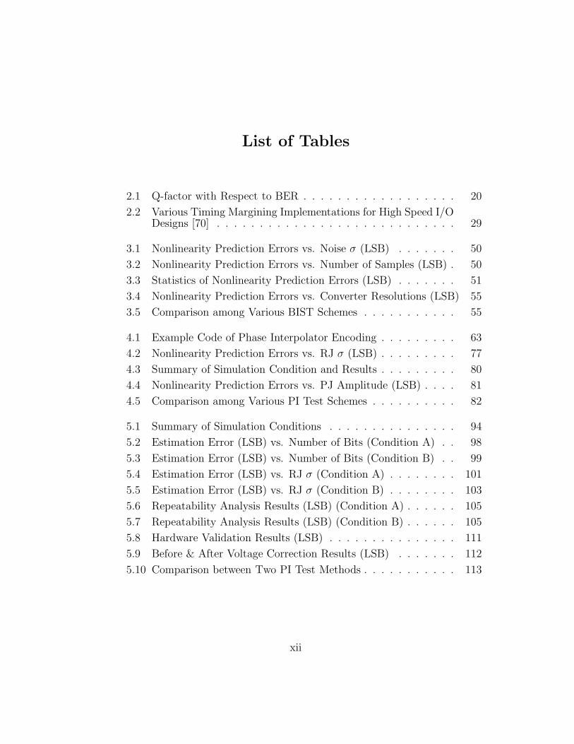
List of Tables
2.1 Q-factor with Respect to BER . . . . . . . . . . . . . . . . . . 20
2.2 Various Timing Margining Implementations for High Speed I/ODesigns [70] . . . . . . . . . . . . . . . . . . . . . . . . . . . . 29
3.1 Nonlinearity Prediction Errors vs. Noise σ (LSB) . . . . . . . 50
3.2 Nonlinearity Prediction Errors vs. Number of Samples (LSB) . 50
3.3 Statistics of Nonlinearity Prediction Errors (LSB) . . . . . . . 51
3.4 Nonlinearity Prediction Errors vs. Converter Resolutions (LSB) 55
3.5 Comparison among Various BIST Schemes . . . . . . . . . . . 55
4.1 Example Code of Phase Interpolator Encoding . . . . . . . . . 63
4.2 Nonlinearity Prediction Errors vs. RJ σ (LSB) . . . . . . . . . 77
4.3 Summary of Simulation Condition and Results . . . . . . . . . 80
4.4 Nonlinearity Prediction Errors vs. PJ Amplitude (LSB) . . . . 81
4.5 Comparison among Various PI Test Schemes . . . . . . . . . . 82
5.1 Summary of Simulation Conditions . . . . . . . . . . . . . . . 94
5.2 Estimation Error (LSB) vs. Number of Bits (Condition A) . . 98
5.3 Estimation Error (LSB) vs. Number of Bits (Condition B) . . 99
5.4 Estimation Error (LSB) vs. RJ σ (Condition A) . . . . . . . . 101
5.5 Estimation Error (LSB) vs. RJ σ (Condition B) . . . . . . . . 103
5.6 Repeatability Analysis Results (LSB) (Condition A) . . . . . . 105
5.7 Repeatability Analysis Results (LSB) (Condition B) . . . . . . 105
5.8 Hardware Validation Results (LSB) . . . . . . . . . . . . . . . 111
5.9 Before & After Voltage Correction Results (LSB) . . . . . . . 112
5.10 Comparison between Two PI Test Methods . . . . . . . . . . . 113
xii

List of Figures
1.1 High Speed Interface Bit Rate Trend [8] . . . . . . . . . . . . 2
2.1 Forwarded Clock Scheme . . . . . . . . . . . . . . . . . . . . . 11
2.2 Embedded Clock Scheme . . . . . . . . . . . . . . . . . . . . . 13
2.3 Clock and Data Recovery Block Diagram [82] . . . . . . . . . 13
2.4 Time Interleaved Transmitter [102] . . . . . . . . . . . . . . . 15
2.5 10GBASE-T Block Diagram [7] . . . . . . . . . . . . . . . . . 16
2.6 BER vs. Sampling Time [87] . . . . . . . . . . . . . . . . . . . 17
2.7 Jitter Decomposition Hierarchy . . . . . . . . . . . . . . . . . 18
2.8 Incorrect Extrapolation Example [87] . . . . . . . . . . . . . . 21
2.9 High Speed I/O Loopback Test Configuration [65] . . . . . . . 23
2.10 On-chip Timing Margining Concept [70] . . . . . . . . . . . . 25
2.11 Loopback vs. Actual Pass/Fail Result Analysis [84] . . . . . . 26
3.1 Test Procedure . . . . . . . . . . . . . . . . . . . . . . . . . . 35
3.2 Proposed Loopback Setup . . . . . . . . . . . . . . . . . . . . 36
3.3 Loopback Conversion Process . . . . . . . . . . . . . . . . . . 37
3.4 LFSR Based Random Noise Generator [10] . . . . . . . . . . . 39
3.5 Random Noise Generator Based on Thermal Noise Amplifica-tion [39] . . . . . . . . . . . . . . . . . . . . . . . . . . . . . . 39
3.6 Random Noise Generator Using Delta-Sigma Modulation [10] . 39
3.7 Loopback Response Comparison with Added Gaussian Noise . 41
3.8 ADC Test Procedure . . . . . . . . . . . . . . . . . . . . . . . 43
3.9 Estimated DAC Output Points from Each ADC Code Transi-tion Voltages . . . . . . . . . . . . . . . . . . . . . . . . . . . 45
3.10 DNL Prediction Errors vs. Noise σ . . . . . . . . . . . . . . . 48
3.11 INL Prediction Errors vs. Noise σ . . . . . . . . . . . . . . . . 49
3.12 DNL Prediction Errors vs. Number of Samples . . . . . . . . . 51
xiii

3.13 INL Prediction Errors vs. Number of Samples . . . . . . . . . 52
3.14 Prediction Errors of ADC Nonlinearities . . . . . . . . . . . . 53
3.15 Prediction Errors of DAC Nonlinearities . . . . . . . . . . . . 54
3.16 DNL Prediction Errors vs. Converter Resolutions . . . . . . . 56
3.17 INL Prediction Errors vs. Converter Resolutions . . . . . . . . 57
4.1 Forwarded Clock Scheme . . . . . . . . . . . . . . . . . . . . . 60
4.2 Derived Clock Scheme . . . . . . . . . . . . . . . . . . . . . . 60
4.3 Phase Interpolator Schematic . . . . . . . . . . . . . . . . . . 61
4.4 Example Bathtub Curve of Receiver . . . . . . . . . . . . . . . 64
4.5 Proposed Configuration for Forwarded Clock Scheme . . . . . 64
4.6 Proposed Configuration for Derived Clock Scheme . . . . . . . 65
4.7 Test Procedure . . . . . . . . . . . . . . . . . . . . . . . . . . 67
4.8 Undersampling Technique . . . . . . . . . . . . . . . . . . . . 69
4.9 Piecewise Cubic Polynomial Interpolation of Dpos . . . . . . . 71
4.10 Delay Adjustment Circuit Architecture Used for Jitter Injec-tion [53] . . . . . . . . . . . . . . . . . . . . . . . . . . . . . . 73
4.11 Timing Generator Block Diagram [34] . . . . . . . . . . . . . . 74
4.12 RJ Injection Circuitry Block Diagram [34] . . . . . . . . . . . 74
4.13 Injected DNL vs. Predicted DNL . . . . . . . . . . . . . . . . 75
4.14 Injected Random Jitter vs. Prediction Error . . . . . . . . . . 77
4.15 Number of Bits in Alternating Data Sequence vs. PredictionError . . . . . . . . . . . . . . . . . . . . . . . . . . . . . . . . 78
4.16 Monte Carlo Simulation of the Proposed Technique . . . . . . 79
4.17 Injected Periodic Jitter vs. Prediction Error . . . . . . . . . . 81
5.1 Undersampling Technique Concept . . . . . . . . . . . . . . . 86
5.2 Test Procedure . . . . . . . . . . . . . . . . . . . . . . . . . . 88
5.3 Circuit Configuration Concept . . . . . . . . . . . . . . . . . . 88
5.4 Estimation Error vs. Size of Window (Condition A) . . . . . . 95
5.5 Estimation Error vs. Size of Window (Condition B) . . . . . . 96
5.6 Estimation Error vs. Number of Bits (Condition A) . . . . . . 97
5.7 Estimation Error vs. Number of Bits (Condition B) . . . . . . 97
xiv
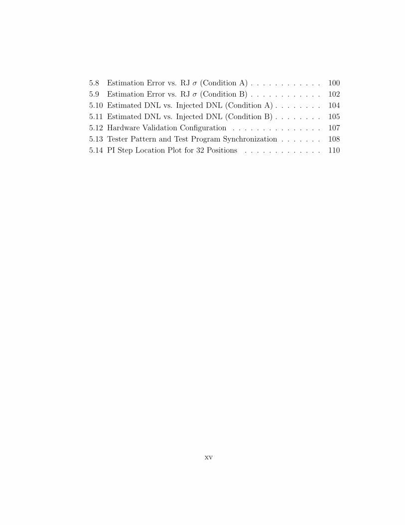
5.8 Estimation Error vs. RJ σ (Condition A) . . . . . . . . . . . . 100
5.9 Estimation Error vs. RJ σ (Condition B) . . . . . . . . . . . . 102
5.10 Estimated DNL vs. Injected DNL (Condition A) . . . . . . . . 104
5.11 Estimated DNL vs. Injected DNL (Condition B) . . . . . . . . 105
5.12 Hardware Validation Configuration . . . . . . . . . . . . . . . 107
5.13 Tester Pattern and Test Program Synchronization . . . . . . . 108
5.14 PI Step Location Plot for 32 Positions . . . . . . . . . . . . . 110
xv

Chapter 1
Introduction
1.1 Motivation
The growing demand for high performance computing systems has
driven the bandwidth increase of chip-to-chip data communications. Tradi-
tional interconnect schemes which use parallel data transfer with low speed
inputs/outputs (I/Os) are limited by technical difficulties such as data timing
alignment and high pin count issues. In order to achieve the goal of multi-
gigabit transfer rates, the traditional I/O structures are replaced by indus-
trial I/O designs such as PCI ExpressTM [5], XAUITM [3], Serial ATATM(S-
ATATM) [11], QuickPath InterconnectTM(QPITM) [59], and HyperTransportTM [2],
etc. These designs have adopted a serial interconnect scheme to resolve timing
skew and high pin count issues in conventional parallel data transfer schemes.
Although the serial interface bit rate increases rapidly, testing of the
high speed serial interfaces becomes a significant challenge due to their speed
and architecture. Figure 1.1 illustrates the speed trend projection of the serial
interface reported by International Technology Roadmap for Semiconductors
(ITRS) [8]. In year 2010, it is not uncommon to find 10 Gbps bit rate inter-
faces. The trend indicates that the high speed serial interfaces would reach
1

Figure 1.1: High Speed Interface Bit Rate Trend [8]
100 Gbps in a next decade or so. Conventional test methods use automated
test equipment (ATE) which has a direct connectivity to the interface of the
device under test (DUT). Since the speed of the interface increases in a short
period of time, the ATE needs to be upgraded to test the interface at speed.
The cost of investment to upgrade the ATE hardware is high which becomes
a major hindrance when using external equipment to test the serial interfaces.
Another challenge on high speed interface test is attributed to the trend
of modern VLSI design methodology. Traditional mixed signal components
have been designed with sufficient design margins to guardband from unex-
pected yield loss due to process and design variations. Nowadays, however,
design methodology for modern processors is trending to system on chip (SOC)
2
development methodology to meet the time-to-market requirement, where the
individual functional components such as serial interface circuits are delivered
as intellectual property (IP) blocks. Integration issues such as coupling noise
between digital and mixed signal circuits degrade the performance of the se-
rial interface blocks, which adversely impacts the design margin during the
integration stage. With ever increasing challenges on data rate requirements
which also forces design to comply with less design margin, the margin be-
comes smaller which leaves more burdens on testing, since not only the data
rate of the I/O but also the accuracy of the test hardware increases the testing
cost. Cost factors to improve equipment’s edge placement accuracy as well as
to design sophisticated signal traces on the load board to ensure the signal in-
tegrity are typical examples that precision test equipment is required to screen
subtle defects.
I/O loopback test [20, 60, 65, 67, 70, 81, 95] has been gaining popularity
as a cost effective alternative for high speed serial interface testing. In this
technique, the transmitter (TX) output is connected to the receiver (RX)
input, and the TX transmits data stream to the RX which requires no direct
interface connections to the external equipment. In order to determine whether
the actual signal eye meets or exceeds the eye mask specification, either passive
device on the loopback path or design for testability (DFT) features such as
timing and voltage margining are used to reduce the size of the signal eye
margin. Despite its popularity, loopback test has limitations such as fault
masking and non-ideality problem on margining circuitry which are described
3

in detail in Chapter 2.
The focus of the dissertation is to develop cost effective yet accurate
test techniques for high speed serial interfaces. The limitations of loopback
tests are studied and innovative test methods to overcome the limitations are
proposed to achieve test completeness.
1.2 Contributions of the Dissertation
In this dissertation, novel test techniques are proposed to address issues
and limitations of the current loopback technique. The contributions of the
dissertation are summarized as follows.
• Development of I/O test methodologies that provide additional coverage
while not disrupting existing test methods.
Fault masking and non-ideality of margining circuits are studied and
three test methodologies are proposed to resolve the issues. The goal of
the dissertation is to develop a methodology that can resolve the known
loopback testing issues while keeping the existing loopback configuration
intact.
A pulse amplitude modulation (PAM) signaling scheme is used in many
serial interface architectures to increase the transfer rate by creating
the symbols with various voltage levels. Analog to digital and digital
to analog converters (ADC and DAC) are used to implement a PAM
signaling scheme as a receiver and a transmitter respectively; however
4

the loop back test of the data converters suffers from fault masking.
The proposed method in Chapter 3 resolves the fault masking issues in
loopback configuration of the DAC and ADC pair.
Timing margining of the current loopback test has a limitation in that
the margining is expected to be uniformly spaced. In real silicon, how-
ever, the phase interpolator circuit which provides the timing margining
capability is not linear and is susceptible to process, voltage, and tem-
perature (PVT) variations. Nonlinearity of the phase interpolator can
result in false fail or false pass of the test which are translated to yield loss
or test escapes. Two techniques to measure the nonlinearities of phase
interpolators are proposed. Both techniques configure the transmitter
and the receiver in the loopback test mode. The first technique utilizes
random jitter injected on the loopback path to provide the reference dis-
tribution to extract nonlinearities. While the method provides accurate
estimates of the nonlinearities, it has a limitation in that it needs to have
a random jitter source on the load board. The second method does not
require the random jitter source on the load board in order to extract
nonlinearity information. Instead, it calculates nonlinearity based on an
intrinsic jitter distribution and a sliding window search algorithm.
• Development of cost effective I/O test methodologies.
As previously mentioned, due to the concern on the increasing test cost,
cost effectiveness of the test methods is an important factor when adopt-
5

ing the technique. In terms of external tester resource usage, our meth-
ods do not require the contact of the external hardware on the high speed
I/O interfaces, since all the proposed test techniques operate in loopback
test mode configurations. Although additional hardware is needed for
the random jitter injection technique, the random jitter source is cheaper
when compared to the precision ATE hardware that operates at speed.
From the silicon design perspective, the proposed methods may require a
few wires or multiplexing logics to enable the proposed test mode, which
do not require major circuit modification to enable the proposed test
methods, since the assumption is that the loopback test mode configu-
ration is already implemented in the silicon.
Since the proposed method provides additional coverage over the current
loopback test configuration, it can be used in wafer level tests, where the
signal integrity of the wafer probe is worse than that of package level
tests, hence less coverage is guaranteed when testing high speed I/Os.
Early identification of the defective part in wafer level test leads to overall
test cost savings since the packaged part is not built based on defective
die.
• Development of HVM test pattern and program that incorporate the
proposed algorithm.
The sliding window algorithm was designed to fit into low cost HVM
tester environment where the response capture memory is limited. With
6

the same low cost HVM tester configuration that can be used for pro-
duction tests, the proposed nonlinearity test algorithm was implemented
in the tester environment. A pattern and test program synchronization
architecture which aligns clock timing between various pattern generator
modules was proposed and implemented in the ATE. The method was
demonstrated to provide an accurate estimation of nonlinearity with-
out additional capital investment on the test hardware. System board
to tester correlation was performed to validate the accuracy of the pro-
posed methodology. The results suggest that the proposed algorithm
provides an accurate estimation of the nonlinearity of the phase interpo-
lator circuitry.
1.3 Organization of the Dissertation
The rest of the dissertation is organized as follows. Chapter 2 presents
an overview of high speed serial link architectures. Signaling and clocking
schemes of the serial interface are explained. Test requirements and related
work are also discussed along with details of the limitations of previous tech-
niques. Based on the limitations, subsequent chapters present proposed test
methodologies to overcome the limitations.
Chapter 3 describes a novel technique for testing the linearity of on-chip
high speed data converters in the loopback configuration. With a loopback
setup and additional noise in the middle of the loopback path, differential
nonlinearities (DNLs) and integral nonlinearities (INLs) of analog-to-digital
7

converters (ADCs) and digital-to-analog converters (DACs) are extracted by
the proposed algorithm. The proposed method exploits the fact that loop-
back output code distribution is distorted by nonlinearities of the ADC when
Gaussian noise is present. From this fact, we can fully characterize the ADC,
without dependency of the DAC characteristics. Then, from the combined
loopback response and the extracted characteristics of the ADC, DAC test is
performed and nonlinearities of the DAC are calculated to construct full ADC
and DAC linearity profiles. Experimental results show that the proposed al-
gorithm can predict INL and DNL of the data converters accurately.
Chapter 4 explains a novel linearity test technique for the margining
circuitry. Using a random jitter injection technique that can be implemented
on the load board using a separate jitter injection source, jitter distribution is
collected using two different sampling techniques such as undersampling and
phase interpolator sampling. The difference between the collected distributions
is attributed to the nonlinearities of the phase interpolators. This fact can be
used to derive the nonlinearity of the phase interpolator circuitry. Experimen-
tal results show that the proposed method provides accurate estimations of
the linearity of the margining circuitry.
Although the method proposed in Chapter 4 presents a novel test
methodology to characterize the margining circuit’s linearity, it requires a
random jitter source on the load board to inject random jitter to estimate the
linearity. Chapter 5 presents a high volume manufacturing (HVM) friendly
technique to measure the linearity, which does not require the random jitter
8

source on the load board. Rather than using the injected random jitter, an
intrinsic jitter distribution is used to construct the profile of the distribution.
A sliding window search algorithm is developed to accurately estimate the
linearity from the collected distribution. The algorithm is computationally
simple to implement in a low cost HVM tester environment. The algorithm
was implemented in a low cost HVM test environment to assess the feasibility
and validity of the method. The experimental results indicate that the method
can accurately predict the nonlinearity of the phase interpolators.
Chapter 6 concludes the dissertation and highlights potential future
research areas in high speed I/O tests.
9
Chapter 2
Design and Test of High Speed Serial I/Os
In this chapter, we review high speed serial interface architecture along
with the challenges for which the architecture provides solutions. An overview
of serial interface test requirements is presented and limitations are discussed.
2.1 Overview of High Speed Interface Scheme
High speed serial interfaces achieve multi-giga transfer rates by resolv-
ing several technical obstacles. In this section, we review the timing alignment
and data rate considerations which are key aspects of high speed serial inter-
face to enable the high data transfer rate.
2.1.1 Timing Alignment Consideration
As the data transfer rate increases, the unit interval (UI) of the bit is
proportionally reduced. For example, the UI of 10 Gbps data rate is 100 psec.
In a conventional parallel data transfer scheme in which the data transfer rate
is increased mainly by increasing the number of pins, aligning the clock signal
with respect to the UI of the data is a significant challenge. Entire board
traces which correspond to the I/Os of two communicating chips need to be
10

Channel D QD QData
Local Clock
TX RX
PIChannel
Figure 2.1: Forwarded Clock Scheme
designed to match the latency within a margin of the half of UI when using
a single clock signal to sample the data. This requirement is a very difficult
one to achieve, since the data rate of the signal is in a multi-Gbps range, and
subsequently the UI is in a range of several hundred picoseconds.
In high speed serial interface schemes, the data is serialized to allevi-
ate the challenge of timing alignment among multiple data signals to a single
clock signal. The transmitter of the serial interface serializes the data, and the
receiver de-serializes the received bit stream to reconstruct the data stream.
While the serializer-deserializer (SerDes) architecture overcomes the difficulty
of the board level latency matching problem across multiple data signals, tim-
ing alignment between a data signal and a clock is still challenging. SerDes
resolves this issue in two different schemes which are described as follows.
2.1.1.1 Forwarded Clock
In a forwarded clock scheme, the clock signal is generated from the
transmitter and sent along with the data stream via another channel as de-
scribed in Figure 2.1.
11

This scheme ensures that the clock frequency of the receiver end is
identical to the transmitter one as the source of the clock is the transmitter.
When the data and the clock signals reach the receiver, the alignment may
not hold, since the trace length of the data channel and the clock channel may
not be identical. In general, the timing skew between data and clock signal
is mitigated by a phase interpolator circuitry. The phase interpolator takes
two different phase signals and creates an intermediate phase signal based
on mixture of the two signals. It takes digital control signals to control the
percentage of the phase mixture, which provide a finer delay control feature
based on the digital code, hence programmable delay of several picoseconds
can be achieved. During power up sequence of the I/O interface, a pre-defined
training sequence is executed to align the timing and exchange configuration
parameters between the transmitter and the receiver. After this sequence,
the phase interpolator is programmed to delay the clock signal by a certain
amount that the training algorithm has found.
The forwarded clock scheme is mainly adopted in industry I/Os such
as QuickPath InterconnectTM(QPITM) [59], Fully Buffered DIMMTM(FBDTM,
FB-DIMMTM) [1], etc.
2.1.1.2 Embedded Clock
Another approach to align data signal timing with the clock signal is
to generate a clock signal from the data bit stream. Figure 2.2 illustrates the
topology of the embedded clock scheme, which is also called a derived clock
12

Channel D QD QData
Local Clock
TX RX
CDR
Figure 2.2: Embedded Clock Scheme
Figure 2.3: Clock and Data Recovery Block Diagram [82]
scheme. In this architecture, the clock signal is generated from the receiver
end and the signal transition of the data bit stream is used to recover the clock.
Clock and data recovery (CDR) circuitry is used to recover the clock from the
signal transitions of the data bit stream. Figure 2.3 describes a block diagram
for a typical CDR circuit. Although there are other variations of CDR designs
such as phase interpolator based design, the generic CDR circuit’s building
blocks are very similar to the ones in a phase locked loop (PLL) design.
Since proper data transition is essential to avoid clock frequency drift,
an encoding scheme is used to maintain the number of transitions. 8 bit to 10
bit (8b/10b) encoding is one of the popular approaches that allows the clock
recovery circuit to construct proper sampling clock at the receiver end. The
13

recovered clock is properly delayed to align with the center of the data bit’s
UI to ensure the correct sampling of the data.
Embedded clock scheme is adopted in many industrial I/O architectures
such as PCI ExpressTM [5], XAUITM [3], HyperTransportTM [2], etc.
2.1.2 Data Rate Consideration
In order to achieve a high data rate, the serial interfaces use either
time interleaving or multi-level signaling [102]. In time interleaving schemes,
transmitter and receiver contain more than one instance of the transmitter
and the receiver respectively. When N transmitters are wired in parallel and
each of them operates at a slightly different time in a staggered way, they can
generate N times of data stream as compared to the one of a single transmit-
ter. Most high speed serial links use 2-way time interleaving which requires to
sample at the rising and falling edge of the clock and effectively reduces down
the operating speed of the rest of the logic by half. A time interleaved trans-
mitter is illustrated in Figure 2.4. In this design, two clock signals are used
to determine when to enable each transmitter to interleave the transmission.
Depending on the design preference, this design can be modified to use 4 clock
signals and use only the rising edges of the clock.
In multi-level signaling, rather than using traditional two voltage levels
which are high and low, more than two levels of voltage can be used. Since
intermediate voltage levels are available for signaling purposes, more than 1
bit can be associated to the various voltage levels. In communication theory,
14

TX TXTXTX
Phase a Phase b Phase c Phase d
Phase a Phase b Phase c Phase d
Clk A
Clk B
Figure 2.4: Time Interleaved Transmitter [102]
this scheme is called pulse amplitude modulation (PAM) where amplitude of
the pulse creates a unique symbol which corresponds to multiple bits [76].
The transmitter and the receiver circuits are designed as a digital to analog
converter (DAC) and an analog to digital converter (ADC) respectively to
enable the pulse amplitude modulation (PAM) signaling scheme.
In industrial designs, 10GBASE-T [7] and other ethernet standards are
using the PAM signaling scheme. Figure 2.5 illustrates a 10 Gbps physical
layer (PHY) block diagram which uses ADC and DAC pair and digital signal
processing (DSP) modules to achieve multi-level signaling and equalization.
15

Figure 2.5: 10GBASE-T Block Diagram [7]
2.2 Test of High Speed Interface
2.2.1 BER and Jitter
The quality of the communication interface is measured by bit error
rate (BER) metric. BER is defined as follows.
BER =Number of Received Bits in Error
Total Number of Transmitted Bits(2.1)
Modern industry standard I/O specifications require a BER of 10−12 or
lower to ensure the quality. The conventional method to test BER at various
error rates is to use external equipment such as bit error rate tester (BERT)
in which a pattern generator, a transmitter, a receiver and a comparison logic
for error detection are implemented. When testing 10 Gbps serial interface
using the conventional method, it takes from several minutes to even a few
hours to collect statistically meaningful data at BER of 10−12 level [21], which
is test time prohibitive for high volume manufacturing. Since one of the major
16

Figure 2.6: BER vs. Sampling Time [87]
contributors to the BER is jitter, understanding jitter and BER relationship
is important. When the timing jitter probability density function (PDF) is
given as f01(∆t) for 0-1 transition and f10(∆t) for 1-0 transition, the overall
BER cumulative density function (CDF) is given as [63]:
F (ts) = P01
∫ ∞
ts
f01(∆t)d∆t + P10
∫ ts
−∞f10(∆t)d∆t (2.2)
where P01 and P10 represent transition densities for 0-1 and 1-0 transitions
respectively. An example BER CDF with respect to sampling time ts in X
axis is illustrated in Figure 2.6.
Describing BER as a function of jitter has an advantage in that total
jitter can be further separated in various jitter components. Total jitter can
be separated to deterministic jitter (DJ) and random jitter (RJ) components.
DJ and RJ are further separated to the following categories [63]. Figure 2.7
illustrates the decomposition hierarchy for various jitter components.
17

TJ
DJ RJ
PJ BUJ DDJ
DCD ISI
Figure 2.7: Jitter Decomposition Hierarchy
2.2.1.1 Deterministic Jitter (DJ)
Deterministic jitter can be separated into data dependent jitter (DDJ),
periodic jitter (PJ), and bounded uncorrelated jitter (BUJ). DDJ can be fur-
ther divided into duty cycle distortion (DCD) and inter symbol interference
(ISI). DCD is a special type of DDJ when the data pattern is a clock like pat-
tern, i.e. 1010. DDJ generally occurs due to the loss of the signal’s frequency
component when the data bit stream is transmitted through the lossy channel.
PDF for DDJ is defined as
fDDJ(∆t) =
N∑
i=1
P DDJi δ(∆t − DDDJ
i ) (2.3)
where P DDJi is the probability for the DDJ value of DDDJ
i .
PJ, also called as sinusoidal jitter (SJ), is a repeating jitter at a certain
18

period or frequency. PDF for PJ is defined as
fPJ(∆t) =1
π√
1 − (∆t/A)2(2.4)
where A is the amplitude of the PJ and −A ≤ ∆t ≤ A. BUJ generally occurs
due to crosstalk and due to its nature of the source, it is bounded. The PDF
is a truncated Gaussian which can be defined as
fBUJ(t) = pBUJ√2πρBUJ
e− t2
2ρ2BUJ for |t| ≤ ABUJ (2.5)
= 0 for |t| > ABUJ (2.6)
where ABUJ represents the peak value, ρBUJ is the sigma value, and pBUJ is
the normalization probability for the BUJ PDF.
2.2.1.2 Random Jitter (RJ)
Random jitter is caused by thermal noise, 1/f flicker noise, shot noise,
or other unbounded jitter source which can be modeled as Gaussian white
noise. Gaussian jitter PDF is defined as
fGJ(∆t) =1√2πσ
e−(∆t−µ)2
2σ2 (2.7)
where, µ represents the mean of the Gaussian distribution and σ represents
its standard deviation.
Due to the RJ component in a total jitter form, the total jitter is
unbounded and a bit error would occur to keep the BER greater than 0. Since
the RJ component is the contributor for the unbounded nature for the TJ, by
19

BER Q(BER)
10−7 5.19910−8 5.61210−9 5.99810−10 6.36110−11 6.70610−12 7.03510−13 7.34910−14 7.651
Table 2.1: Q-factor with Respect to BER
separating the RJ and the DJ components from the TJ, we can extrapolate the
TJ at certain BER level. Tailfit algorithm is a popular method to decompose
the jitter components based on Gaussian tail of the TJ distribution [63]. Once
the DJ and RJ components are determined, the TJ at certain BER can be
written as
TJ(BER) = DJ + 2Q(BER)σRJ (2.8)
where, σRJ is standard deviation of the RJ. The Q-factor values are given as
shown in Table 2.1.
Modern BERT systems support a timing scan function in which edge
placement of the clock can be varied to provide multiple data points to create
a BER curve. Some of them also support a built in function to extrapolate
the obtained BER curve. This can be viewed as a similar method to the
jitter decomposition since random jitter is dominant at lower BER level, hence
extrapolation is more accurate if the BER is measured at lower BER level.
Correct selection of extrapolation point is essential, since extrapolation at an
20

Figure 2.8: Incorrect Extrapolation Example [87]
incorrect point could result in over- or underestimation of the BER at the 10−12
level. An example incorrect extrapolation due to this problem is illustrated
in Figure 2.8. In this figure, extrapolation at higher BER level denoted as µ′L
and µ′R caused an overestimation of RJ as compared to the real RJ µL and
µR.
2.2.2 Built in Self Test (BIST) of High Speed Interface
In order to resolve the test cost issue, adoption of built in self test
(BIST) methods has become an attractive solution. The BIST methods en-
able testing of the devices using on-chip test circuitry. Without relying on
costly automated test equipment (ATE), the BIST methods provide effective
solutions to test high speed serial links [22, 70, 81, 90]. Authors in [22, 90] use
on-chip circuitry such as flip-flops and vernier delay lines to characterize the
21

jitter. Although they can provide jitter measurements without using ATE,
they cannot enable at-speed functional testing of the digital logics in the serial
links when the methods are used alone. Therefore, there needs to be a way to
enable at-speed testing of the interface without depending on the ATE.
2.2.3 Loopback Test
Loopback based testing schemes [20, 60, 65, 67, 70, 81, 95], on the other
hand, have been gaining popularity since they provide a way to exercise the
interface without depending on the ATE. In loopback test configuration, both
jitter tolerance and logics in the physical layer of the high speed links can be
tested at speed.
Figure 2.9 illustrates a typical loopback configuration. In the loopback
scheme, the output node of the transmitter is connected to the input node of
the receiver so that transmitted data can be easily compared with received
data on the same device. The transmitter is driving the receiver at speed to
screen any delay defects on the serial links. With the loopback scheme, it
is required to determine whether the actual signal eye meets or exceeds the
eye mask specification. There are various techniques to achieve the margining
capability. One solution is to use external jitter injection filters in the loopback
channel to margin the timings and voltages of the data eye [20]. The other
one is to implement a design for testability (DFT) feature by reusing existing
circuitry in high speed links to enable the margining capability [67, 70]. Since
it is difficult to inject an exact amount of jitter using the external filters, the
22

Figure 2.9: High Speed I/O Loopback Test Configuration [65]
23

reuse of the existing circuitry is a preferred way to implement the margining
capability. Although there has been some success on controlling the injected
jitter amount [65], the loopback with the DFT based eye margining approach
has been widely adopted in many industrial high speed I/O tests, because it
is rather simple and easy to implement in existing high speed I/O schemes.
2.2.4 On-chip Timing Margining Implementation
The timing margining concept is described in Figure 2.10. In general,
the clock signal is placed at the center of the data eye to ensure proper data
latching with low BER. The on-chip margining capability enables capability
to move the clock placement by the desired amount. Since the clock and data
recovery (CDR) architecture determines how to align the clock with the data,
the on-chip margining capability implementation takes the CDR architecture
as a baseline, and enables the margining capability by adding additional cir-
cuits for controllability. This approach minimizes area overhead associated
with timing margining implementation.
On-chip timing margining capability provides a similar function as the
timing scan in a BERT where the BER is measured at certain locations of the
clock edge to obtain BER curve. By assessing BER at certain timing location,
or simply determining pass/fail at the timing location with pre-determined
guardband, we can achieve low cost HVM test of the high speed I/Os without
requiring expensive external equipment.
24
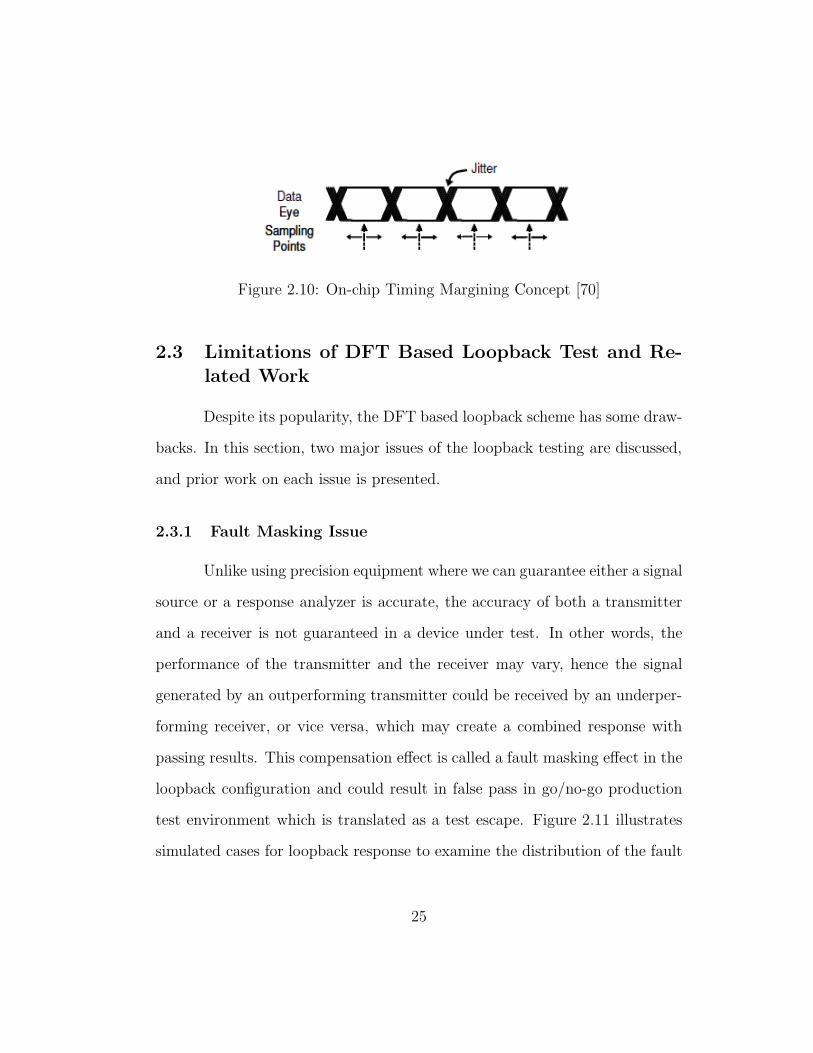
Figure 2.10: On-chip Timing Margining Concept [70]
2.3 Limitations of DFT Based Loopback Test and Re-
lated Work
Despite its popularity, the DFT based loopback scheme has some draw-
backs. In this section, two major issues of the loopback testing are discussed,
and prior work on each issue is presented.
2.3.1 Fault Masking Issue
Unlike using precision equipment where we can guarantee either a signal
source or a response analyzer is accurate, the accuracy of both a transmitter
and a receiver is not guaranteed in a device under test. In other words, the
performance of the transmitter and the receiver may vary, hence the signal
generated by an outperforming transmitter could be received by an underper-
forming receiver, or vice versa, which may create a combined response with
passing results. This compensation effect is called a fault masking effect in the
loopback configuration and could result in false pass in go/no-go production
test environment which is translated as a test escape. Figure 2.11 illustrates
simulated cases for loopback response to examine the distribution of the fault
25

Figure 2.11: Loopback vs. Actual Pass/Fail Result Analysis [84]
masking issue. In this Monte-Carlo simulation example, 2200 ensembles were
generated with statistically induced errors and 8% of the distribution indi-
cates either false fail or false pass cases. 6.5% of the distribution shows fault
masking which is a significant portion of the distribution.
The fault masking issue becomes more challenging when pulse ampli-
tude modulation (PAM) scheme is used for high speed serial links [32, 106]; this
architecture uses high speed analog to digital converters (ADCs) and digital
to analog converters (DACs) for the interfaces to perform multi-level signaling
and equalization. In the PAM architecture, since the linearity of data convert-
ers determines the bit error rate (BER) of the link, linearity characterization
without the fault masking effect is very important when testing data converter
pairs in the loopback mode.
Although there are many proposed methods [12, 15, 80, 98] to test only
one type of the data converters, either ADC or DAC, which use extra logic to
26

test the data converters, they may not be desirable ways to perform testing
for high speed I/O cases where both types of data converters are available,
which causes the area overhead to double. Schemes that test both converters
are proposed as well [13, 47, 96]. Compared to the methods above, these are
optimized in terms of area for both converter tests. However, they still have
some area overhead since they also have extra hardware for BIST implemen-
tation. In terms of test time, they test each converter sequentially, and thus
test time doubles when we test both converters. Moreover, some of the tech-
niques [47, 98, 103] exploit certain circuit blocks in ADC or DAC to achieve the
BIST technique without significant area overhead; however, availability of the
specific functional blocks may limit the general application of those methods.
There are some previous papers to test data converters in a loopback
configuration. In [108], delta-sigma data converters in the loopback mode are
used as a study case to separate the ADC and DAC characteristics. However,
the application of the method is limited to delta-sigma type data converters, so
it cannot be easily generalized. Shin et al. [84] propose a loopback characteris-
tic separation methodology based on loopback response of the data converters
when the loopback path has an analog filter. With the presence of the analog
filter on the loopback path, the response from the DAC is attenuated, then
the attenuated response is converted to digital code by the ADC. From the
difference of the loopback responses, the characteristics of the ADC and the
DAC are extracted. Park et al. [75] propose a parallel test method to separate
ADC’s and DAC’s characteristics using an analog summer and an RMS de-
27

tertor. The aforementioned approaches focus on dynamic specifications of the
data converters in loopback configuration which may have less importance,
when testing data converters used for the multi-level signaling drivers and
receivers.
For static specification such as nonlinearity characterization methods
in loopback mode, Yu et at. [109] propose a statistical method based on noise
characterization to calculate nonlinearities of data converters in the loopback
test mode. However, this method is not appropriate for separating character-
istics of each converter without monitoring an internal node, which is difficult
in today’s system on chip (SOC) development practices, where I/O designs are
delivered as hard IP (Intellectual Property) blocks. Shin et al. [85] propose
using a digital equalizer to calibrate the DAC prior to the loopback mode test
to separate the data converter characteristics, which may have dependency on
availability of such an equalizer for data converters. Due to the equalization
procedure which is pre-requisite, the two step operations of the test sequence
may require longer test time. Our proposed method to resolve the fault mask-
ing issue in a loopback configuration without the aforementioned dependencies
is presented in Chapter 3.
2.3.2 Margining Circuitry Linearity Issue
In general, the timing margining capability in loopback test is enabled
by using phase interpolator (PI) circuitry when it is enabled by the internal
circuitry reuse. Table 2.2 summarizes various implementations for on-chip
28

Interface CDR Type and Methods Range Resolution
S-ATA Over-sampled; 2 UI 1/8 UITX phase select
PCI Express PI based; 2 UI 1/32 UISupplemental or offset
DMI PI based; 2 UI 1/32 UISupplemental
FBD PI based; 2 UI 1/32 UIOffset
Table 2.2: Various Timing Margining Implementations for High Speed I/ODesigns [70]
timing margining capability for high speed I/Os. Although one design adopts
oversampling based clock and data recovery (CDR) circuits which determines
timing margining capability to be implemented as TX phase select method,
most of the designs use PI based CDR, hence the implementation of the timing
margining capability is based on the PI circuits.
The phase interpolators are used to margin the timing of the data
eye to identify the total jitter from a given set of data pattern and to screen
defective parts if the jitter exceeds the allowed amount in the specification. As
another application of PI, Casper et al. [68] implement an on-die oscilloscope
to measure the timing aspects of the signal, and the PI is used to scan the
signal boundary with respect to timing. In both cases, in order to ensure the
validity of the measured data, the linearity of the phase interpolator should
be fairly good. However, in real manufacturing cases, process, voltage and
temperature (PVT) variation significantly affects the linearity of the PI in
each die. The PVT impact becomes more severe in today’s highly advanced
29

process technologies since the variation tends to increase as the size of device
shrinks; therefore, it is necessary to find a way to test the linearity of phase
interpolator itself in a cost effective manner.
Conventional methods for testing the linearity of typical analog mix-
ers may include direct measurement of phase relationships for various phase
configurations. However, this approach is difficult to apply to PIs in high
speed I/O applications since the resolution of interpolated phases needs to be
in the unit of the several picoseconds and measuring of the subtle difference
is a significant challenge. This challenge becomes more obvious when using
external equipments such as ATEs due to signal integrity and loading effect is-
sues at high speeds. To relieve this issue, measuring linearities at lower speeds
can substitute for high speed measurement. However, at-speed measurement
is becoming more important, since at-speed measurement of linearity shows
differences from the measurements at lower speeds.
There is some previous work regarding linearity test techniques for the
PI. Provost [77] proposes a PI linearity measurement technique that requires
an additional phase interpolator to determine whether each PI satisfies speci-
fications in terms of linearity. Shi et al. [83] introduce self test circuitry which
is composed of a phase detector, a phase-difference-to-voltage converter, an
analog-to-digital converter (ADC) and control logic. While it is possible to
measure the linearity of PIs using these techniques, both these techniques re-
quire large amounts of on chip real estate as compared to that for the PI which
raises yield concern since the probability of defects in the test logic becomes
30

greater as the size of the logic increases. Our proposed methods to resolve this
issue are presented in Chapter 4 and 5.
31

Chapter 3
Efficient ADC and DAC Loopback Test
A pulse amplitude modulation (PAM) signaling scheme is used in many
serial interface architectures to increase the transfer rate by creating the sym-
bols with more voltage levels. Analog to digital and digital to analog converters
(ADC and DAC) are used to implement the PAM signaling scheme, however
loopback test of the data converters suffers from the fault masking issue.
In this chapter, we propose a new methodology which provides complete
linearity characterization with a proposed loopback mode setup. It exploits a
Gaussian noise added loopback scheme of DAC and ADC to obtain simplicity
and facility of implementation.
This chapter is organized as follows. Section 3.1 reviews definition
of converter errors. Section 3.2 explains proposed methodology. Simulation
results are presented in Section 3.3 and comparison with prior work is presented
in Section 3.4. Section 3.5 presents other factors to consider when applying
the proposed method. Section 3.6 summarizes the chapter.
32

3.1 Review of Converter Linearity Errors
Among all the DC characteristics of converters, the linearity test con-
sumes the largest portion of test time since it is required to test entire codes
with a large number of samples. Various definitions of DNL and INL have been
introduced [19], and the most common definition of data converter linearity
errors is used for this chapter.
For N code converters, ith endpoint DNLs of DAC and ADC are defined
as follows.
DNLDAC(i) =V (i + 1) − V (i)
V LSBDAC
− 1 (3.1)
where,
V LSBDAC =
∑N−1i=1 V (i + 1) − V (i)
N
V (i) is ith output voltage level.
DNLADC(i) =CT (i + 1) − CT (i)
V LSBADC
− 1 (3.2)
where,
V LSBADC =
∑N−1i=1 CT (i + 1) − CT (i)
N
CT (i) is ith code transition voltage. Since our definition for DNLs are endpoint
DNLs, integration of the DNLs yields endpoint INLs. For N code converters,
ith endpoint INLs of DAC and ADC are defined as follows.
INLEP (i) =i
∑
k=1
DNL(k)
33

From the endpoint INLs, we can derive best-fit INLs by
INLBF (i) = INLEP (i) − max(INLEP ) + min(INLEP )
2(3.3)
The max() and min() functions yield maximum and minimum values among
all INLEP s respectively. All DNLs and INLs are in units of LSB. We se-
lected the definitions of endpoint DNLs and best-fit INLs for evaluation of our
proposed algorithm.
3.2 Proposed Technique
Figure 3.1 illustrates test procedure of the proposed method. First,
inherent or deliberately created Gaussian random noise is injected in the mid-
dle of the loopback path. Next, a varied linear histogram testing method
is performed for our scheme explained in the next subsection. We supply a
slowly increasing finite resolution ramp generated by a DAC to the input of an
ADC. Unlike the traditional linear histogram testing method [66], we record
the number of code occurrences in a matrix H , for each ADC output code
and each DAC voltage level. Compared to other data converter test methods
in earlier literature in which data from data converters are collected in a se-
quential manner, our method simultaneously collects data for both converters,
which provides advantage in terms of test time. From the collected data in
matrix H , we can calculate ADC’s DNLs and INLs. Then, we can calculate
DAC’s DNLs and INLs based on both the collected data and the calculated
ADC’s characteristics.
34

Inject Gaussian
Noise in the
loopback path
Transmit Certain
Number of
Samples per Code
of DAC
Create Code
Occurrence
Histogram H from the
Loopback Response
Calculate ADC
Nonlinearities
Calculate DAC
Nonlinearities
Figure 3.1: Test Procedure
35

Noise
DAC ADCDigitalInput Output
Digital
Figure 3.2: Proposed Loopback Setup
3.2.1 Loopback Configuration
Figure 3.2 is the proposed loopback setup. In this setup, DAC output
is connected to ADC input so that we can handle the input and output of
the setup in digital by CPU or DSP units. This loopback setup has several
advantages. First, it allows us to test the ADC and the DAC simultaneously
which reduces test time. Second, we don’t need additional hardware to achieve
BIST. Third, since the test algorithm can be run as software, there is more
flexibility. Finally, this is an appropriate approach for routine monitoring
during operation. Despite those prominent advantages, nonlinearity extraction
for each converter is difficult due to fault masking. Recently, however, it has
been shown that linearity of ADCs can be fully tested with a finite resolution
ramp [69]. According to this paper, considering appropriate amount of noise
at ADC input, we can use an imperfect ramp, i.e., staircase output from DAC
in order to calculate the accurate code transition voltages of the ADC. Based
on this fact, we add random noise in the middle of the loopback path. The
noise can be either inherent or deliberately added. Thermal noise and noise
from other circuitry are major sources for the inherent noise. Dithering is a
common technique to improve ADC’s linearity by adding noise [101].
36

�����
�����
����������������������
����������������������
������������������������������
������������������������������
������
������
���
�����������
k
C’k(l−2) C’klC’k(l+3)
k(l−1)C’ klC’k(l−2)C’ k(l+1)C’ k(l+2)C’ k(l+3)C’
DAC��������������
������������������������������������
������������������������������������
������������������������������������������
������������������������������������������
����������������������������������������������������������������
����������������������������������������������������������������
����������������������������������������������������������������������������������������������������������������������������������������������������������������
����������������������������������������������������������������������������������������������������������������������������������������������������������������
���������������������������������������������
���������������������������������������������
������������������������������
������������������������������
0
Gaussian Noise
Gaussian Input Signal to ADC Code Occurrence Histogram
Area divided by unequally sized bins
k
C
V
kVf
ADC
g
Figure 3.3: Loopback Conversion Process
37

Although inherent noise from circuits may be enough for specific ap-
plications of the proposed method, precise Gaussian noise may be required in
other applications where test precision is one of the important factors. In this
case, we can implement Gaussian random noise injection circuitry to facilitate
the requirement. Many techniques have been proposed to implement Gaus-
sian noise injection circuits [10, 39]. One technique utilizes pseudo-random
sequence generation capability of LFSR (Linear Feedback Shift Register) [10].
In this technique, LFSR output is connected to a low pass filter through a level
shifter to generate analog random noise based on the pseudo-random sequence
from LFSR as shown in Figure 3.4. The drawback of this method is that the
generated distribution is not strictly Gaussian. Also the mean and the variance
of the distribution are not well controlled by users when using this method.
Another technique is to use thermal noise from resistors and to amplify it to
generate random noise [39]. Figure 3.5 illustrates the topology of the thermal
noise amplification method. This method produces an accurate Gaussian noise
distribution; however it may produce different results due to process variation
of the circuitry. Our method does not require a tightly controlled Gaussian
noise source as shown in the simulation result section. However, the user may
require a parameter control capability on the generated noise for various rea-
sons such as additional debug capability on the signal sources. In such cases,
delta-sigma modulation based Gaussian noise shaping proposed in [10] can be
used to implement such a noise source with a full parameter control capability.
Figure 3.6 illustrates the block diagrams of the noise generator architecture.
38

Figure 3.4: LFSR Based Random Noise Generator [10]
Figure 3.5: Random Noise Generator Based on Thermal Noise Amplifica-tion [39]
Figure 3.6: Random Noise Generator Using Delta-Sigma Modulation [10]
39

The loopback conversion process is explained in Figure 3.3. Suppose
that we have the kth digital code, Ck. This code is converted to an analog
voltage, Vk by the DAC. Since the DAC’s characteristics uniquely determine
Vk for Ck, if the DAC has nonlinearities, the voltage level of Vk is slightly
different from an ideal DAC. Gaussian noise is added before the signal enters
the ADC. With the assumption that the noise is Gaussian with zero mean and
σ2 variance, the input signal of the ADC has its mean at the DAC’s output
voltage and variance of σ2. The ADC divides the area of Gaussian probability
density function (PDF) of signal with respect to its code transition voltages. If
the ADC is completely linear, all code transition voltages are equally spaced,
and thus it produces a Gaussian shaped code occurrence histogram that has
a mean at the center code, C ′kk. However, because of nonlinearities, the ADC
divides the PDF unequally, which results in a code occurrence histogram not
similar to Gaussian distribution. Figure 3.7 illustrates the effect of Gaussian
noise when injected in the middle of the loopback path. In an ideal DAC and
ADC loopback pair, the Gaussian distributions are equally spaced, which is
attributed to the linearity of the DAC. The linear ADC produces Gaussian
code occurrence since the locations of code transition voltages, which deter-
mine the size of code bins, are also equally spaced. However, in a non-ideal
loopback pair case, the nonlinearity of the DAC may position the means of
Gaussian PDFs in a non-uniform manner. Also the nonlinearity of ADC may
produce non-trivial code occurrence histogram due to non-uniform code tran-
sition voltage locations.
40

Figure 3.7: Loopback Response Comparison with Added Gaussian Noise
41

Suppose that f and g represent code conversion functions of the DAC
and the ADC respectively. A digital code Cin is converted to analog by f(Cin).
Because the noise (E) is added in the middle, the digital loopback output is
represented by Cout = g(E +f(Cin)). Nonlinear functions can be expanded by
Taylor series, hence
Cout =∞
∑
k=0
{f(Cin)}kg(k)(E)
k!
Since f(Cin) is constant and E is converted only by g(k), loopback output code
occurrence histogram is determined by the g(k)(E) term, which means that it
is affected only by the ADC. Thus, the distorted code occurrence histogram is
due only to nonlinearities of the ADC, not those of the DAC.
3.2.2 ADC Test
Figure 3.8 describes the ADC test procedure. Suppose that H is a
matrix that represents the code occurrence histogram. The dimension of H is
m by n where m is the number of codes of DAC and n is the number of voltage
levels of ADC. Each element in H represents the number of code occurrences
for each ADC code and DAC voltage level. The code occurrence histogram
matrix, H is converted to the cumulative distribution function matrix A by
akl =
∑lj=1 hkj
NS
where akl and hkl are the (k,l) elements of A and H respectively, and NS is the
number of samples. Using Gaussian cumulative distribution function (CDF)
that has zero mean and variance of 1, the ADC’s normalized code transition
42
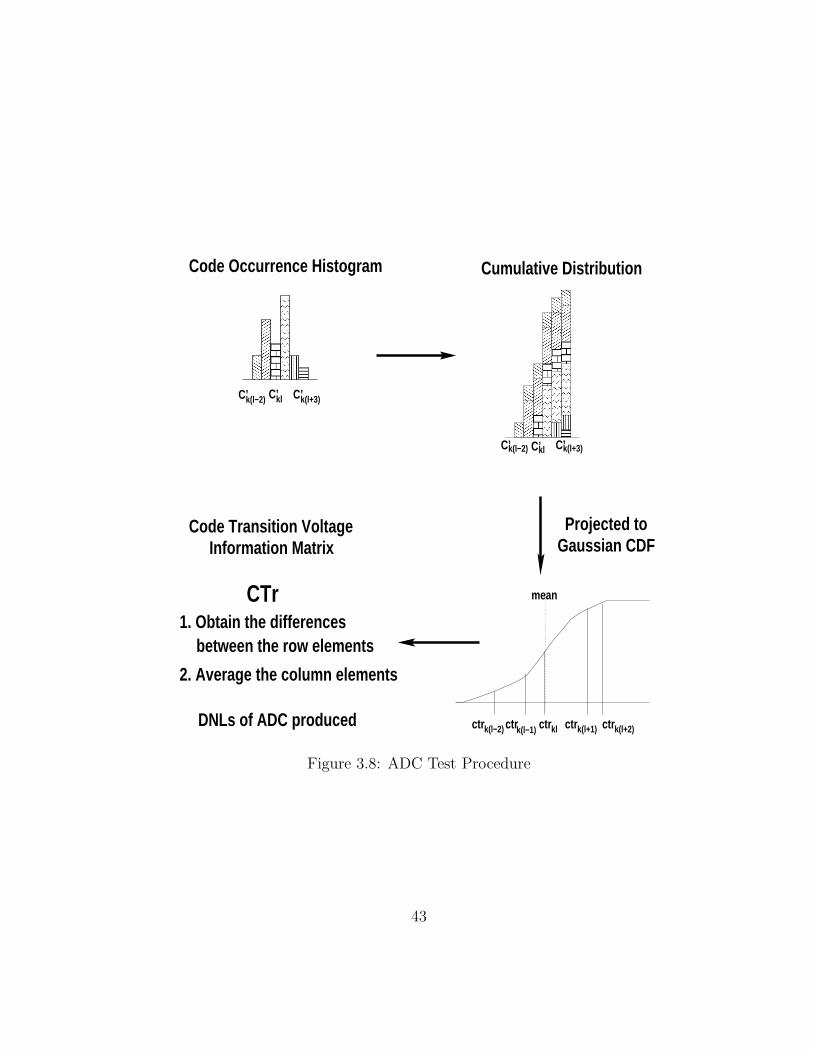
ctr k(l+2)ctr k(l−2) ctrk(l−1) ctr kl ctr k(l+1)
C’k(l−2) C’kl k(l+3)C’
C’k(l−2) C’kl C’k(l+3)
������
������
�����
�����
����������
����������
������������������������������
������������������������������
���������
���������
����
����
����
��������
����
��������
��������
��������������������
��������������������
����
����
�����������
�������
���
���
����������
����������
������������
����������
����������
��������
�������
�������
��������
������
������
����������
����������
����
��������������
��������������
�������
�������
������
������
Code Occurrence Histogram Cumulative Distribution
Gaussian CDF
mean
Projected to
CTr
Code Transition Voltage
1. Obtain the differencesbetween the row elements
2. Average the column elements
Information Matrix
DNLs of ADC produced
Figure 3.8: ADC Test Procedure
43
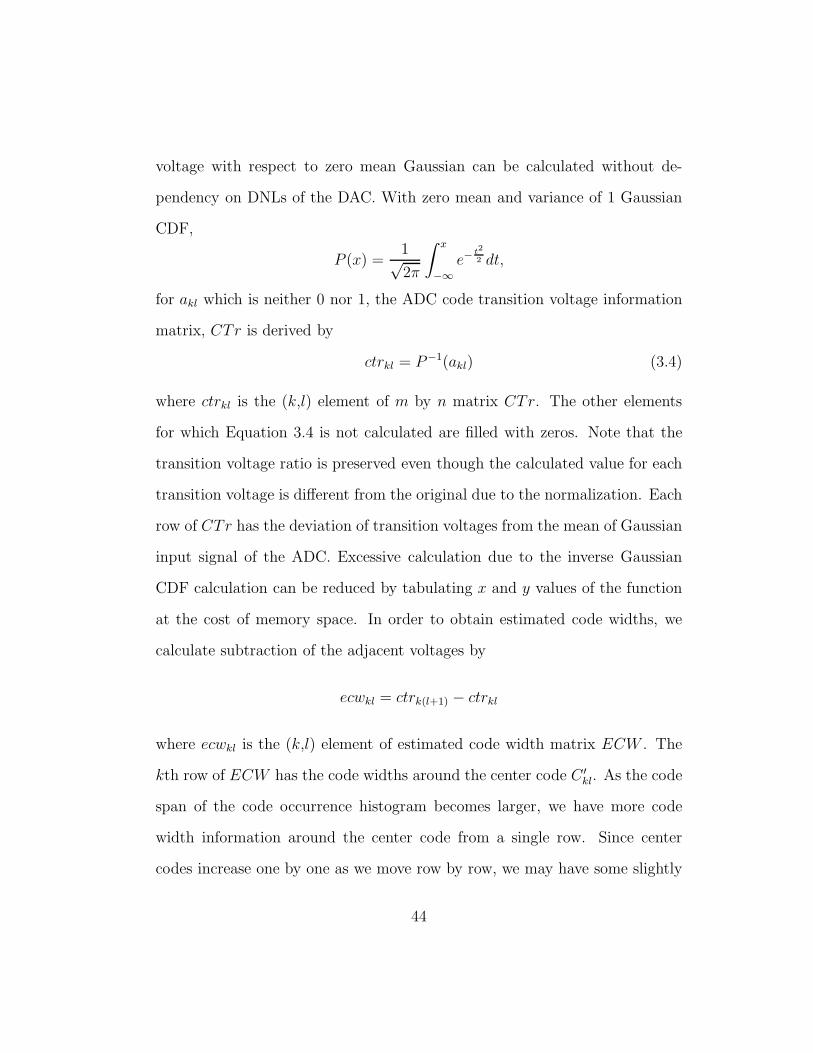
voltage with respect to zero mean Gaussian can be calculated without de-
pendency on DNLs of the DAC. With zero mean and variance of 1 Gaussian
CDF,
P (x) =1√2π
∫ x
−∞e−
t2
2 dt,
for akl which is neither 0 nor 1, the ADC code transition voltage information
matrix, CTr is derived by
ctrkl = P−1(akl) (3.4)
where ctrkl is the (k,l) element of m by n matrix CTr. The other elements
for which Equation 3.4 is not calculated are filled with zeros. Note that the
transition voltage ratio is preserved even though the calculated value for each
transition voltage is different from the original due to the normalization. Each
row of CTr has the deviation of transition voltages from the mean of Gaussian
input signal of the ADC. Excessive calculation due to the inverse Gaussian
CDF calculation can be reduced by tabulating x and y values of the function
at the cost of memory space. In order to obtain estimated code widths, we
calculate subtraction of the adjacent voltages by
ecwkl = ctrk(l+1) − ctrkl
where ecwkl is the (k,l) element of estimated code width matrix ECW . The
kth row of ECW has the code widths around the center code C ′kl. As the code
span of the code occurrence histogram becomes larger, we have more code
width information around the center code from a single row. Since center
codes increase one by one as we move row by row, we may have some slightly
44
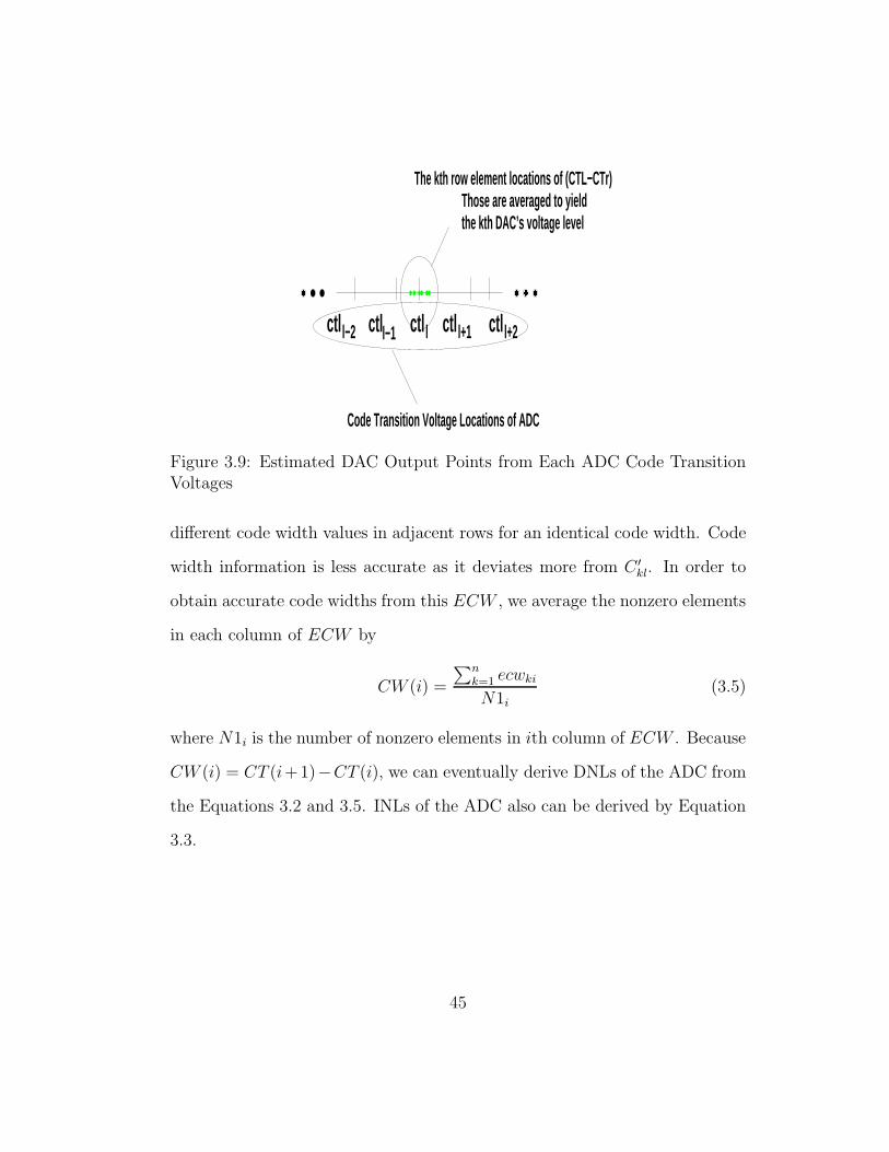
ctl l+2ctl l+1ctl l−2 ctl lctl����
������������
����
l−1
Those are averaged to yield
Code Transition Voltage Locations of ADC
The kth row element locations of (CTL−CTr)
the kth DAC’s voltage level
Figure 3.9: Estimated DAC Output Points from Each ADC Code TransitionVoltages
different code width values in adjacent rows for an identical code width. Code
width information is less accurate as it deviates more from C ′kl. In order to
obtain accurate code widths from this ECW , we average the nonzero elements
in each column of ECW by
CW (i) =
∑nk=1 ecwki
N1i(3.5)
where N1i is the number of nonzero elements in ith column of ECW . Because
CW (i) = CT (i+1)−CT (i), we can eventually derive DNLs of the ADC from
the Equations 3.2 and 3.5. INLs of the ADC also can be derived by Equation
3.3.
45

3.2.3 DAC Test
From the known code widths of the ADC, we can locate the ADC’s
normalized code transition voltages (except for the first and the last code
transition voltage) by
CTLV (i) =
i−1∑
k=0
CW (k)
where CTLV (i) is a row vector of ith code transition voltage location and
CW (0) = 0. As mentioned earlier, CTr from the Equation 3.4 has the de-
viations of transition voltages from the mean of Gaussian input signal of the
ADC. Because we already know accurate code transition voltage locations,
we can exploit this information as an estimation of mean location from each
code transition voltage of the ADC. CTLV is expanded to the same dimension
matrix as CTr by
CTL = Ones(2N) × CTLV
where Ones(2N) is a column vector of all 1s whose length is 2N . After filling
the elements of CTL with zero at the same location as CTr’s zero elements,
each element of (CTL − CTr) indicates an estimated mean location of the
ADC Gaussian input signal. Figure 3.9 describes the estimated DAC voltage
points before average. The mean of the ADC Gaussian input signal is the
output of the DAC before adding the Gaussian noise. Therefore we can derive
normalized voltage level for each DAC output by averaging the row elements
of (CTL − CTr) by
V (i) =
∑nk=1 (ctl − ctr)ik
N2i(3.6)
46

where V (i) is the ith voltage level of the DAC and N2i is the number of
nonzero elements in ith row of (CTL − CTr). As mentioned earlier, not the
real voltage values but the ratios of voltage level are preserved, thus we can
derive DNLs of the DAC by Equations 3.1 and 3.6. INLs of the DAC also can
be derived by Equation 3.3.
3.3 Simulation Results
Simulation by MATLABR© has been performed to validate our method-
ology. First, we modeled an ideal ADC and DAC, and connected them in
loopback mode. Randomly generated nonlinearities were injected into these
models. The DNLs and INLs of the ADC and the DAC were then predicted
by the proposed method. Errors between the originally injected nonlinearities
and the predicted nonlinearities were calculated to measure the accuracy of
our method. During the simulation, we first used 8 bit, 50 MSPS DAC and
ADC, then applied the setup to other bit converters. Reference voltages for
both converters were set to 3V.
Our test methodology requires that some of samples must fall in adja-
cent code bins in order to calculate code widths of the ADC. It needs at least
0.5 LSB deviation in order to move across the code transition voltages. 95% of
samples fall in the deviation of 2σ for Gaussian distribution. Assuming that
at least 5% of code occurrence in adjacent bins is required to calculate code
widths, the noise σ is required to be more than 0.25 LSB.
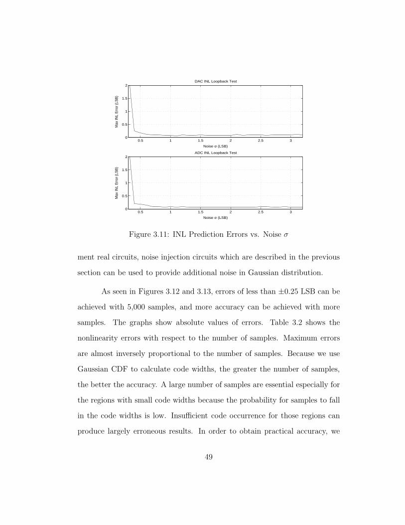
Figures 3.10 and 3.11 show that the relationship between noise stan-
47

0.5 1 1.5 2 2.5 30
0.5
1
1.5
2
Noise σ (LSB)
Max
DN
L E
rror
(LS
B)
DAC DNL Loopback Test
0.5 1 1.5 2 2.5 30
0.5
1
1.5
2
Noise σ (LSB)
Max
DN
L E
rror
(LS
B)
ADC DNL Loopback Test
Figure 3.10: DNL Prediction Errors vs. Noise σ
dard deviation and absolute values of errors. Table 3.1 summarizes the data
for nonlinearity errors with respect to the noise σ. Similar to our analysis, σ of
less than 0.3 LSB couldn’t validate our methodology. The errors were greatly
decreased when the noise σ was increased from 0.3 LSB to 0.6 LSB. Errors
were almost flat once the noise standard deviation exceeded 0.7 LSB. As the
noise σ increases, code span of code occurrence histogram increases. Increased
code span produces more deviated codes which may produce more erroneous
estimations. This results in the slight error increase for the DAC with high
noise σ. However, we can avoid this problem by cutting off largely deviated
data, and thus noise variance is not a very important factor for our method-
ology. For our test, we chose Gaussian noise with zero mean and standard
deviation of 1 LSB. In case the internal noise is insufficient when we imple-
48
0.5 1 1.5 2 2.5 30
0.5
1
1.5
2
Noise σ (LSB)
Max
INL
Err
or (L
SB
)
DAC INL Loopback Test
0.5 1 1.5 2 2.5 30
0.5
1
1.5
2
Noise σ (LSB)
Max
INL
Err
or (L
SB
)
ADC INL Loopback Test
Figure 3.11: INL Prediction Errors vs. Noise σ
ment real circuits, noise injection circuits which are described in the previous
section can be used to provide additional noise in Gaussian distribution.
As seen in Figures 3.12 and 3.13, errors of less than ±0.25 LSB can be
achieved with 5,000 samples, and more accuracy can be achieved with more
samples. The graphs show absolute values of errors. Table 3.2 shows the
nonlinearity errors with respect to the number of samples. Maximum errors
are almost inversely proportional to the number of samples. Because we use
Gaussian CDF to calculate code widths, the greater the number of samples,
the better the accuracy. A large number of samples are essential especially for
the regions with small code widths because the probability for samples to fall
in the code widths is low. Insufficient code occurrence for those regions can
produce largely erroneous results. In order to obtain practical accuracy, we
49

Noise σ DAC DNL Err. ADC DNL Err. DAC INL Err. ADC INL Err.
0.3 1.996 1.907 2.534 2.4530.5 0.077 0.088 0.170 0.1740.7 0.040 0.051 0.094 0.0890.9 0.041 0.036 0.076 0.0741.1 0.046 0.036 0.065 0.0731.3 0.044 0.028 0.081 0.0661.5 0.045 0.022 0.091 0.0761.7 0.059 0.025 0.083 0.0641.9 0.055 0.027 0.077 0.0692.1 0.067 0.030 0.111 0.0722.3 0.060 0.028 0.105 0.0742.5 0.071 0.025 0.106 0.0952.7 0.072 0.025 0.102 0.0742.9 0.091 0.020 0.099 0.0773.1 0.079 0.026 0.114 0.073
Table 3.1: Nonlinearity Prediction Errors vs. Noise σ (LSB)
#Samples DAC DNL Err. ADC DNL Err. DAC INL Err. ADC INL Err.
5,000 0.102 0.082 0.230 0.22010,000 0.081 0.055 0.167 0.14515,000 0.077 0.044 0.107 0.09620,000 0.060 0.043 0.150 0.13325,000 0.054 0.045 0.152 0.11930,000 0.049 0.033 0.112 0.09735,000 0.049 0.035 0.105 0.10240,000 0.047 0.038 0.100 0.11445,000 0.043 0.040 0.083 0.07750,000 0.038 0.027 0.102 0.090
Table 3.2: Nonlinearity Prediction Errors vs. Number of Samples (LSB)
50

0.5 1 1.5 2 2.5 3 3.5 4 4.5 5
x 104
0
0.05
0.1
0.15
0.2
0.25
Number of Samples
Max
DN
L E
rror
(LS
B)
DAC DNL Loopback Test
0.5 1 1.5 2 2.5 3 3.5 4 4.5 5
x 104
0
0.05
0.1
0.15
0.2
0.25
Number of Samples
Max
DN
L E
rror
(LS
B)
ADC DNL Loopback Test
Figure 3.12: DNL Prediction Errors vs. Number of Samples
ADC DNL Err. ADC INL Err. DAC DNL Err. DAC INL Err.
Min -0.038 -0.056 -0.032 -0.032Max 0.026 0.025 0.035 0.060Mean -0.002 -0.013 0.003 0.010STD 0.007 0.013 0.010 0.014
Table 3.3: Statistics of Nonlinearity Prediction Errors (LSB)
set the number of samples as 50,000 at each ADC input level.
Figures 3.14 and 3.15 show that maximum prediction errors of less
than ±0.1 LSB are achieved, which validates our methodology. Table 3.3
summarizes statistics of the prediction errors.
Test time can be approximately determined by
(Number of Codes) × (Number of Samples)
Conversion Speed(3.7)
51

0.5 1 1.5 2 2.5 3 3.5 4 4.5 5
x 104
0.05
0.1
0.15
0.2
0.25
Number of Samples
Max
INL
Err
or (L
SB
)
DAC INL Loopback Test
0.5 1 1.5 2 2.5 3 3.5 4 4.5 5
x 104
0.05
0.1
0.15
0.2
0.25
Number of Samples
Max
INL
Err
or (L
SB
)
ADC INL Loopback Test
Figure 3.13: INL Prediction Errors vs. Number of Samples
=28 × 50, 000
50 × 106= 0.256 sec
Since constructing the code transition voltage information matrix can be per-
formed concurrently with entering input samples and counting the number
of code occurrence, total test time is 0.256 + δ second which is considered a
reasonable test time. As expected, there is a tradeoff between test time and
accuracy. As the number of samples increases, test time also increases while
the errors decrease.
With the selected noise σ and the number of samples, we simulated
other resolution converters. Figures 3.16 and 3.17 show our scheme has less
than ±0.1 LSB errors for the converters of 4 to 18 bits. Even though errors
are small enough in high resolution, it is more appropriate to use this method
52

0 50 100 150 200 250
−0.1
−0.05
0
0.05
0.1
Code Index
Err
or (L
SB
)
Difference between Original and Predicted ADC DNLs
50 100 150 200 250
−0.1
−0.05
0
0.05
0.1
Code Index
Err
or (L
SB
)
Difference between Original and Predicted ADC INLs
Figure 3.14: Prediction Errors of ADC Nonlinearities
for the high speed, medium resolution (6 to 12 bits) converters because of the
test speed determined by Equation 3.7. Table 3.4 summarizes the nonlinearity
errors with respect to the converter resolutions.
3.4 Comparison with Prior Work
A comparison of our method with other methods in [47, 85] is summa-
rized in Table 3.5. Note that the previously mentioned methods in [15, 16] are
not included in this comparison as they are only applicable to ADC tests. This
comparison is based on 8 bit data converters with maximum 3 LSB nonlinear-
ity errors. Note that our method does not have hardware overhead other than
circuits associated with enabling loop test mode on the assumption that we
have on-chip DSP or CPU units which can process the digital input and out-
53

0 50 100 150 200 250
−0.1
−0.05
0
0.05
0.1
Code Index
Err
or (L
SB
)
Difference between Original and Predicted DAC DNLs
50 100 150 200 250
−0.1
−0.05
0
0.05
0.1
Code Index
Err
or (L
SB
)
Difference between Original and Predicted DAC INLs
Figure 3.15: Prediction Errors of DAC Nonlinearities
put of the loopback pair. From the assumption that the loopback test mode is
already available in the ADC and DAC test pair, the proposed method is most
cost effective as well as reasonably accurate among the state-of-art techniques.
The proposed method does not depend on data converter architecture which
is another advantage of the technique, unlike the method in [47]. Although
the test times are not reported in the comparison cases, test time is expected
to be shorter than [85] since it does not require multiple steps to calculate
nonlinearities of the data converters.
3.5 Other Considerations
Although the proposed method successfully predicts the linearities of
data converters, the method relies on the Gaussian randomness of the noise
54

#Bits DAC DNL Err. ADC DNL Err. DAC INL Err. ADC INL Err.
4 0.024 0.027 0.027 0.0185 0.025 0.017 0.029 0.0226 0.026 0.027 0.042 0.0397 0.035 0.026 0.050 0.0548 0.035 0.027 0.078 0.0849 0.037 0.039 0.099 0.09610 0.039 0.037 0.080 0.07111 0.034 0.028 0.099 0.09312 0.040 0.033 0.080 0.06713 0.048 0.028 0.085 0.08714 0.037 0.032 0.095 0.09715 0.037 0.035 0.100 0.09216 0.035 0.028 0.081 0.07617 0.039 0.034 0.093 0.08118 0.042 0.038 0.087 0.099
Table 3.4: Nonlinearity Prediction Errors vs. Converter Resolutions (LSB)
Our Method Huang et al. [47] Shin et al. [85]
Max Error ≤ 0.1 LSB 0.05 LSB 0.67 LSBNo significant LPF, Digital
additional circuits Analog equalizerrequired comparator,
Area ControlOverhead unit,
(Additional Counter,Circuits) Memory,
SwitchesType All types Delta-Sigma All types
Test Time < 0.3 sec N/A N/A
Table 3.5: Comparison among Various BIST Schemes
55

4 6 8 10 12 14 16 180
0.05
0.1
0.15
0.2
Number of Bits
Max
DN
L E
rror
(LS
B)
DAC DNL Loopback Test
4 6 8 10 12 14 16 180
0.05
0.1
0.15
0.2
Number of Bits
Max
DN
L E
rror
(LS
B)
ADC DNL Loopback Test
Figure 3.16: DNL Prediction Errors vs. Converter Resolutions
distribution. This, in turn, may imply that the injected noise distribution,
which may not be perfectly Gaussian in real applications, could cause addi-
tional errors on top of the factors that are analyzed in this chapter. In the real
application, careful characterization of the proposed method may be required
to adjust skew of the prediction errors due to the imperfect Gaussian noise
source. Since the randomness of the Gaussian noise is more important in the
proposed method than the parameters such as variance, users may implement
additional random noise source for which various schemes are reviewed in the
previous section.
56

4 6 8 10 12 14 16 180
0.05
0.1
0.15
0.2
Number of Bits
Max
INL
Err
or (L
SB
)
DAC INL Loopback Test
4 6 8 10 12 14 16 180
0.05
0.1
0.15
0.2
Number of Bits
Max
INL
Err
or (L
SB
)
ADC INL Loopback Test
Figure 3.17: INL Prediction Errors vs. Converter Resolutions
3.6 Summary
In this chapter, we propose a novel methodology to test linearity of
ADC and DAC. With the loopback setup with additional Gaussian noise, a
novel test methodology is developed, which enables us to calculate nonlineari-
ties of ADC and DAC respectively. Accurate DNLs and INLs of each converter
are successfully extracted regardless of fault masking. Other than interconnec-
tion and test mode switches, no additional hardware is necessary as compared
to other BIST schemes.
Since the proposed method is a system level approach, it can be applied
to all ADC and DAC topologies. Compared to testing with automated test
equipment (ATE) or other BIST circuitry, this approach is cost effective and
57

facilitates implementation.
58

Chapter 4
Phase Interpolator Test Using a Random
Jitter Injection
Non-ideality of margining circuit can lead to an incorrect assessment
of the timing margin when a DFT based loopback test is used to screen the
I/O defects. In this chapter, a new method to measure the linearity of PI code
steps without significant hardware overhead is proposed. Using a random
jitter (RJ) source on the load board, RJ is injected into the data channel
when the data channel is configured as a loopback mode. The amount of the
injected jitter needs to be adjusted such that it can barely close the data eye.
The distribution of the random jitter is captured by two different methods,
which are undersampling and sampling using phase interpolator code sweeping.
Then, the two results are compared and predicted differential nonlinearities
(DNLs) are derived using a series of mathematical calculations.
This chapter is organized as follows. In Section 4.1, we explain various
high speed I/O schemes and basic operation of phase interpolator circuitry.
The motivation of the proposed technique is also described in the section. In
Section 4.2, the proposed technique is explained in detail. Simulation results
and comparison with state-of-art techniques follow in Sections 4.3 and 4.4
59
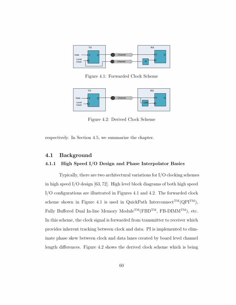
Channel D QD QData
Local Clock
TX RX
PIChannel
Figure 4.1: Forwarded Clock Scheme
Channel D QD QData
Local Clock
TX RX
CDR
Figure 4.2: Derived Clock Scheme
respectively. In Section 4.5, we summarize the chapter.
4.1 Background
4.1.1 High Speed I/O Design and Phase Interpolator Basics
Typically, there are two architectural variations for I/O clocking schemes
in high speed I/O design [63, 72]. High level block diagrams of both high speed
I/O configurations are illustrated in Figures 4.1 and 4.2. The forwarded clock
scheme shown in Figure 4.1 is used in QuickPath InterconnectTM(QPITM),
Fully Buffered Dual In-line Memory ModuleTM(FBDTM, FB-DIMMTM), etc.
In this scheme, the clock signal is forwarded from transmitter to receiver which
provides inherent tracking between clock and data. PI is implemented to elim-
inate phase skew between clock and data lanes created by board level channel
length differences. Figure 4.2 shows the derived clock scheme which is being
60

V2V1
Vout
I1 I2 I3 I4
R1 R2
T1 T2 T3 T4 T5 T6 T7 T8
Figure 4.3: Phase Interpolator Schematic
used in PCI express, Serial ATA, etc. In this scheme, the clock signal is de-
rived from data transitions in data signal using clock and data recovery (CDR)
circuitry. While the derived clock scheme uses fewer number of pins since it
does not need a clock channel, the data signal is required to provide a suffi-
cient number of transitions to guarantee proper clock signal generation at the
receiver side. 8b/10b encoding is a popular scheme to provide necessary signal
transitions. Although typical CDRs are designed using a structure similar to
a PLL, PI based CDR scheme is gaining popularity due to its fast acquisition
time as well as lower area overhead and better stability control.
Figure 4.3 describes a circuit level diagram of a typical phase interpo-
lator circuit implementation [58]. The output voltage Vout achieved by this
circuitry can be expressed as follows.
Vout = a1V1 + a2V2 (4.1)
61
where a1 and a2 are weighted factors which can be realized by adjustable
current sources (I1 through I4). If V1 and V2 are identical sinusoidal signals
with the phase difference of 90◦, Equation 4.1 can be rewritten as follows.
Using trigonometric identities, we obtain:
Vout = sin(ωt)cos(α) + cos(ωt)sin(α)
= sin(ωt + α) (4.2)
where
V1 = sin(ωt), V2 = cos(ωt) = sin(ωt + 90◦)
a1 = cos(α), a2 = sin(α)
Thus, it is shown that the phase of Vout is shifted by α.
In many phase interpolator designs, the adjustable current sources that
determine the coefficients can be digitally controlled so that the possible set
of interpolation can be uniformly distributed. Each digitally encoded code
is mapped to specific current value of the current source, thus it can achieve
a specific degree of interpolation. An example encoding of PI is shown in
Table 4.1.
Some phase interpolation designs use multiple phase interpolators to
implement high resolution PI circuitry [49]. In one scheme, instead of using
just one PI with in-phase and quadrature phase inputs to create uniformly
distributed middle phase outputs, a network consisting of a coarse resolution
interpolation circuit and multiple fine resolution PIs is used. Although this
scheme can increase the resolution of the PI by reducing the burden of fine
62

Index Code Phase Degree
1 0000 0◦
2 0001 10◦
3 0010 20◦
4 0011 30◦
......
...9 1000 80◦
Table 4.1: Example Code of Phase Interpolator Encoding
tuning of adjustable current sources, it increases the size of the circuitry, thus
becoming more likely to be defective or more sensitive to process variation in
the manufacturing process.
4.1.2 Impact of Nonlinearity of PI
One may ask whether several picoseconds of nonlinearity in PIs would
make a significant difference in high speed I/O performance. To illustrate
the point, we use an example bathtub curve that is captured from a high
speed serial link. Figure 4.4 is drawn based on measurement data from [18].
The curve on the left side shows that it takes about one step of the phase
interpolator’s position to change bit error rate (BER) from 10−12 to 10−9.
This can be translated to 132
UI or 3.125 psec, thus 3.125 psec of jitter can
degrade BER from 10−12 to 10−9.
Addition of a small amount of total jitter can degrade the BER sig-
nificantly due to the sharp slope of the bathtub curve which results from
characterization of most multi gigahertz high speed I/O. If the differential
nonlinearity (DNL) of the PI in the region of the eye boundary is δ and the
63

−20 −15 −10 −5 0 5 10 15 2010
−12
10−10
10−8
10−6
10−4
10−2
100
Phase Interpolator Position
BE
R
Figure 4.4: Example Bathtub Curve of Receiver
measured total jitter using a timing margining technique is Jtotal, the worst
case real jitter can be given as δ+Jtotal, which could exceed specification limits
depending on the test conditions, with the risk of defective part escapes.
D QD QData
Local Clock
TX RX
PI
Random Jitter Injection
Separate Clock Source
Figure 4.5: Proposed Configuration for Forwarded Clock Scheme
64

D QD QData
Local Clock
TX RX
PI
Random Jitter Injection
Separate Clock Source
PI Based CDR
Figure 4.6: Proposed Configuration for Derived Clock Scheme
4.2 Overview of The Proposed Technique
The configurations for our proposed technique to measure nonlinearity
of PI are described in Figures 4.5 and 4.6. We configure the transmitter
(TX) and receiver (RX) such that the data channels are connected together.
This can be either through a loopback configuration on a single device or by
connecting two identical devices by pairing up TX and RX. A separate clock
source is introduced to undersample the data. The quality and the cost of the
clock source are not of concern as high quality and low jitter clock source can
be implemented on-board with low cost [90]. For the forwarded clock scheme,
the clock channel is directly connected to the undersampling clock source as
shown in Figure 4.5. For the derived clock scheme, we use a multiplexer to
reach the PI in the CDR block as shown in Figure 4.6. With this configuration,
we follow the following steps to predict the PI linearity.
Figure 4.7 illustrates the steps to test the PI with the proposed tech-
nique. First, the data port sends an alternating data pattern, i.e., the 1010
sequence to the channel. The jitter injection shown in the figure does not
occur at this step. Depending on the clocking scheme of the high speed serial
65

link, we undersample the data by injecting a clock signal with the period of
T +∆T , where T is a data signal period. When we undersample the signal, we
select ∆T to be the same as the phase resolution or code step of the PI. Since
the PI is connected to the clock signal path, we program the PI code such that
PI does not shift the phase of the signal while undersampling the signal. The
collected undersampled data is then stored as the expected bit sequence from
undersampling. Then we supply a normal clock signal with the period of T
and use the PI to sample the alternating data pattern. We collect the sampled
data for each PI code index and store it as the expected bit sequence from PI
sampling for the code index i. We repeat this procedure until we sweep all
combinations of PI codes and collect the sampled data.
Next, we inject random jitter into the data channel with a fair amount
of variance to barely close the data eye. Since random jitter injection occurs in
data channel, jitter injection capability in the system or load board is required.
Then, we undersample and PI-sample the jitter injected data signal with the
same period and steps.
In order to construct the random jitter distribution vector from the in-
jected random jitter in the data channel, error bit sequences EVus and EVps,i
for undersampling and PI-sampling, respectively, are created by comparing the
expected bit sequence with the jitter injected bit sequence. Since we reduce
other interference factors by comparing bits from the same data source, ran-
dom jitter injection is the only difference, and it is ensured that the distribution
from the error bit sequence will be closer to a random Gaussian distribution.
66

Transmit 1010
Pattern through
Data Lane
Characterize the
Transmitted
Pattern with
Undersampling
Chatacterize the
Transmitted
Pattern with PI
Sampling
Map PI Sampling
Distribution to
Undersampling
Dist. to Calculate
DNL
Inject RJ in the
Middle of
Loopback Channel
1. Repeat
the Steps
with RJ
2. Difference Calc. to
Extract Dist.
Figure 4.7: Test Procedure
67

EVus and EVps,i are re-bucketed based on sampling positions of the data eye,
then these distributions are stored in vector Dpos and D′pos, respectively, after
normalization. The distribution vector Dpos represents a random jitter dis-
tribution sampled with ∆T resolution. If we use an ideal PI to characterize
the jitter, the PI sampled distribution, D′pos will be identical to Dpos under
one condition that the PI’s resolution is also ∆T . Since, in reality, the PI is
not ideal and contains nonlinearities, the distribution collected using PI code
sweeping, D′pos will be different from Dpos. Therefore, we can mathematically
derive DNLs from the difference between Dpos and D′pos. The details of the
mathematical algorithm are explained in the following subsections.
4.2.1 Distribution Vector Creation Using Undersampling
Undersampling techniques have been used to measure jitter of high
speed applications [90]. The idea of undersampling technique is illustrated in
Figure 5.1. In Figure 5.1 (a), the period of the data signal is given as T and
the period of the sampling clock is given as T + ∆T . Since the sampling clock
period is delayed by ∆T , every cycle of data signal is sampled with the delay
of ∆T . After we collect all the sampled data and construct the eye diagram,
the equivalent sampling points of the eye diagram are shown in Figure 5.1 (b).
By comparing the sampled jittery bit sequence with the expected bit
sequence, we can derive an error vector EVus and EVps,i where i represents
PI code index. The normalized distribution vectors can be derived by the
following equations.
68

T 2 T 3 T
T
(a) Undersampling of Alternating Data Pattern
(b) Equivalent Sampling of the Pattern
T
. . . . .
. . . . .
Figure 4.8: Undersampling Technique
For all integers i such that 1 ≤ i ≤ T
∆T,
Dpos(i) =
∑lk=0(EVus(i + k T
∆T))
∑lk=1 EVus(k)
(4.3)
D′pos(i) =
∑lk=1 EVps,i(k)
∑li,k=1 EVps,i(k)
(4.4)
where k in the form of EVus/ps,i(k) represents the kth bit in the vectors and
l is the largest number that makes the vector index become the maximum
number.
69

4.2.2 Calculation of Predicted DNL
Based on the jitter distribution, Dpos, which is derived from the under-
sampling technique, we can calculate DNLs of the PI. We consider Dpos as a
golden reference here since it can be assumed to be the identical distribution
when PI DNLs are all zero. To ease the mapping of distribution and the DNLs,
we use a piecewise cubic polynomial interpolation technique [30]. Piecewise
cubic polynomials of Dpos are given as follows.
For i = 0, 1, 2, . . . , n − 1 and xi ≤ x ≤ xi+1,
Si(x) = ai(x − xi)3 + bi(x − xi)
2 + ci(x − xi) + di (4.5)
For Equation 5.5, we need to determine 4n conditions to have an analytic
solution for the equation. The conditions are given as follows.
Si(xi) = yi, for all i = 0, 1, 2, . . . , n,
Si(xi+1) = yi+1, for all i = 1, 2, 3, . . . , n − 1,
S ′i−1(xi) = S ′
i(xi), for all i = 1, 2, 3, . . . , n − 1,
S ′′i−1(xi) = S ′′
i (xi), for all i = 1, 2, 3, . . . , n − 1,
S ′′0 (x0) = S ′′
n−1(xn) = 0. (4.6)
An example of the piecewise cubic polynomial interpolation result is shown
in Figure 4.9. Once we derive the piecewise polynomials from Dpos, we can
create a vector that contains the estimated positions of sampling points of PI.
Given D′pos(i), a piecewise polynomial exists so that Sk−1(k − 1) ≤ D′
pos(i) ≤
Sk(k). Since there exists more than one piecewise polynomial that satisfies the
70

0 10 20 30 40 500
0.01
0.02
0.03
0.04
0.05
0.06
0.07
DataInterpolation Curve
Figure 4.9: Piecewise Cubic Polynomial Interpolation of Dpos
condition, i.e., the distribution is not monotonic but more like a U-shape, we
need to divide the region so that the search space for the solution is always
monotonic. In our algorithm, we divide the search space into two regions:
0 ≤ i ≤ T2∆T
and T2∆T
< i ≤ T∆T
. Then we use the polynomial in an appropriate
region to find a solution of ti which results in Sk−1(ti) = D′pos(i) where k−1 ≤
ti ≤ k. Here, ti represents the predicted position of sampling point for PI code
index i. The predicted DNL for each PI code index i is determined by the
following equation.
DNLi = ti+1 − ti (4.7)
4.2.3 Random Jitter Injection Considerations
The proposed technique requires a random jitter injection module on
the load board to obtain desired distribution. Various schemes have been
71

proposed to enable jitter injection capability [34, 53]. Keezer et al. [53] pro-
pose a delay adjustment circuit which is used to deskew high speed signals.
By performing AC-coupling of a random noise source which represents the
random noise in voltage, the deskew logic is demonstrated to be used as a
random jitter injection circuit. Various random noise sources are discussed in
Chapter 3 which can be used in conjunction with the delay adjustment circuit
to implement the random jitter injection capability. Figure 4.10 depicts the
architecture of the delay adjustment circuit.
Fujibe et al. [34] propose a timing generator based jitter injection ar-
chitecture. The timing generator is used to control the timing of the signal
transitions. With delay control logic and variable vernier delay line which
provide coarse and fine control of the delay, timing data controls the timing of
the signal transitions on cycle by cycle basis. The generator has been designed
with 90nm CMOS technology and supports 6.5 Gbps signals. Figure 4.11
shows basic building blocks of the timing generator. Since we have capability
to control the timings of each bit, we can implement jitter injection capability
by adding the jitter information to the timing data. Figure 4.12 illustrates
the jitter injection capability implementation based on the timing generator
module.
72

Figure 4.10: Delay Adjustment Circuit Architecture Used for Jitter Injec-tion [53]
73

Figure 4.11: Timing Generator Block Diagram [34]
Figure 4.12: RJ Injection Circuitry Block Diagram [34]
74
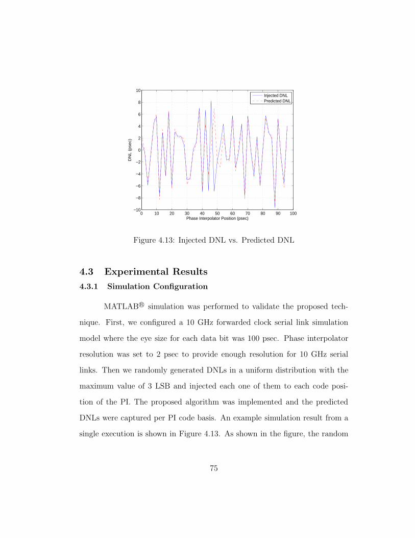
0 10 20 30 40 50 60 70 80 90 100−10
−8
−6
−4
−2
0
2
4
6
8
10
Phase Interpolator Position (psec)
DN
L (
pse
c)
Injected DNLPredicted DNL
Figure 4.13: Injected DNL vs. Predicted DNL
4.3 Experimental Results
4.3.1 Simulation Configuration
MATLABR© simulation was performed to validate the proposed tech-
nique. First, we configured a 10 GHz forwarded clock serial link simulation
model where the eye size for each data bit was 100 psec. Phase interpolator
resolution was set to 2 psec to provide enough resolution for 10 GHz serial
links. Then we randomly generated DNLs in a uniform distribution with the
maximum value of 3 LSB and injected each one of them to each code posi-
tion of the PI. The proposed algorithm was implemented and the predicted
DNLs were captured per PI code basis. An example simulation result from a
single execution is shown in Figure 4.13. As shown in the figure, the random
75
injection of DNLs and the predicted DNLs are tracking each other very well,
except for the center of the PI sampling code.
The prediction error in the central region can be explained as follows.
As the sampling position for the PI code converges to the center of the data
eye, it has a lower number of the histogram samples due to the lower prob-
ability of the occurrence, which results in lower sharpness in the constructed
piecewise cubic polynomial curves. This increases the prediction error rate
since a sharper curve determines a smaller range of values in x axis for a given
range of values in y axis, as compared to a gradual one. Although the predicted
DNLs are less accurate at the central region, our proposed scheme does not
seem to be flawed since the linearity of phase interpolator is more important
in the region of the signal eye boundary, therein BER is determined by sev-
eral picoseconds of jitter. Therefore, we have configured our scheme such that
we ignore the prediction error in the center of the PI code and we obtained
sufficient prediction accuracy with a fair number of transmitted bit sequences.
4.3.2 Simulation Results
To determine the optimal conditions for the simulation, we performed
the following experiments. First, we experimentally studied the impact of
amount of RJ to the prediction accuracy. We increased the amount of the
root mean square (RMS) value of the RJ’s standard deviation (σ) from 1 psec
RMS to 30 psec RMS, and repeated the simulation for each RJ σ value to
analyze the impact. Figure 4.14 shows the simulation results and Table 4.2
76

0 5 10 15 20 25 300
0.5
1
1.5
2
2.5
3
3.5
4
RJ sigma (psec)
Prediction RMS Error (LSB)
Figure 4.14: Injected Random Jitter vs. Prediction Error
RJ σ DNL RMS Error
1 3.8273 2.3725 0.8957 0.5259 0.31311 0.34313 0.39115 0.63017 0.42919 0.88121 0.66723 1.12225 0.70027 0.77929 0.910
Table 4.2: Nonlinearity Prediction Errors vs. RJ σ (LSB)
77

102
103
104
105
106
107
0
0.5
1
1.5
2
2.5
3
3.5
4
Number of Bits
Pre
dic
tion
RM
S E
rro
r (L
SB
)
Figure 4.15: Number of Bits in Alternating Data Sequence vs. PredictionError
summarizes the data. As can be seen, the prediction accuracy increased when
the RJ σ value increased, and when it reached 7 psec the prediction error
reached the lowest level and stayed at this level until the value became 15 psec.
From 15 psec to 30 psec, the prediction error started increasing, showing more
uncertainty for the simulation. This is because two Gaussian distributions of
random jitter at the left and right sides of the signal eye are convolved together
if excessive random jitter exists. This effect reduces the sharpness of the slope
for the distribution thus degrading the prediction performance. Since it did
not show dependency on the amount of RJ σ for the range of 7 psec to 15
psec, we selected 10 psec RMS as a simulation set point.
Next, we experimented on the relationship between the number of
78

0 0.5 1 1.5 2 2.5 30
0.5
1
1.5
2
2.5
3
3.5
Injected DNL RMS (LSB)
Pre
dic
ted
DN
L R
MS
(L
SB
)
Figure 4.16: Monte Carlo Simulation of the Proposed Technique
transmitted bits and prediction accuracy. The result in Figure 4.15 shows
that the prediction error decreases as the number of transmitted bits increases.
Once it reached 500,000 bits, the prediction accuracy became stabilized. We
selected 1 million bit sequences as a simulation set point to obtain an accurate
result with reasonable simulation performance.
Using the selected simulation conditions, we performed a Monte-Carlo
simulation with randomly generated ensembles to determine the repeatability
of our scheme. 100 iterations of this simulation set were performed. Fig-
ure 4.16 describes the result of the simulation. Simulation conditions as well
as resultant mean and standard deviation of the prediction RMS error are
summarized in Table 4.3. As shown in the results, our scheme can predict the
79
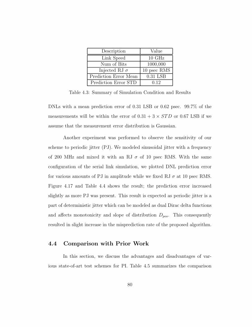
Description Value
Link Speed 10 GHzNum of Bits 1000,000Injected RJ σ 10 psec RMS
Prediction Error Mean 0.31 LSBPrediction Error STD 0.12
Table 4.3: Summary of Simulation Condition and Results
DNLs with a mean prediction error of 0.31 LSB or 0.62 psec. 99.7% of the
measurements will be within the error of 0.31 + 3 × STD or 0.67 LSB if we
assume that the measurement error distribution is Gaussian.
Another experiment was performed to observe the sensitivity of our
scheme to periodic jitter (PJ). We modeled sinusoidal jitter with a frequency
of 200 MHz and mixed it with an RJ σ of 10 psec RMS. With the same
configuration of the serial link simulation, we plotted DNL prediction error
for various amounts of PJ in amplitude while we fixed RJ σ at 10 psec RMS.
Figure 4.17 and Table 4.4 shows the result; the prediction error increased
slightly as more PJ was present. This result is expected as periodic jitter is a
part of deterministic jitter which can be modeled as dual Dirac delta functions
and affects monotonicity and slope of distribution Dpos. This consequently
resulted in slight increase in the misprediction rate of the proposed algorithm.
4.4 Comparison with Prior Work
In this section, we discuss the advantages and disadvantages of var-
ious state-of-art test schemes for PI. Table 4.5 summarizes the comparison
80

0 0.5 1 1.5 2 2.5 3 3.5 4 4.5 50
0.5
1
1.5
2
2.5
PJ Amplitude (psec)
Prediction RMS Error (LSB)
Figure 4.17: Injected Periodic Jitter vs. Prediction Error
PJ Amp. (psec) DNL RMS Error
0 0.2820.5 0.3091 0.341
1.5 0.4302 0.437
2.5 0.5093 0.842
3.5 0.7554 0.905
4.5 1.0675 1.176
Table 4.4: Nonlinearity Prediction Errors vs. PJ Amplitude (LSB)
81

Our Method Provost [77] Shi et al. [83]
Mean Error 0.31 LSB N/A N/AMax Error 0.67 LSB ≥ 1 LSB N/A
No significant Additional PI Phase detector,additional circuits if not avail. Phase-to-voltage converter,
required ADCArea
Overhead(AdditionalCircuits)
Table 4.5: Comparison among Various PI Test Schemes
items. Although our method does not require significant additional logic to
enable PI test capability, mutual PI test scheme [77] requires additional phase
interpolator circuitry if it is not already available in the design. Also the max-
imum prediction error for the method cannot be lower than 1 LSB since the
resolution of the test cannot be better than one PI step.
PI test circuit implementation method described in [83] requires addi-
tional circuits such as a phase detector, a phase-to-voltage converter and an
ADC which consume significant amount of real estate in silicon. Although the
accuracy of the technique is not reported in the literature, PVT variation af-
fects the accuracy of the measurement circuits, hence calibration of the analog
circuitry may be required to obtain desired accuracy, which may increase test
time.
82

4.5 Summary
In this chapter, we proposed an efficient test technique for phase inter-
polators using random jitter injection. The proposed algorithm is cost effective
in that it does not require hardware overhead in the case of forwarded clock
scheme. For the derived clock scheme, we only need to implement one mul-
tiplexer in the clock lane to implement clock injection capability. The load
board or system board only needs to contain a random jitter injector and a
clock generator for undersampling purpose. The proposed algorithm based
on statistical data collection and curve fitting scheme accurately predicts the
DNL of the phase interpolator. Simulation results show that our method ac-
curately predicted nonlinearities of the PI. Since our method does not require
significant circuit changes, it can be easily applied to various high speed I/O
microarchitectures where PI is used.
This method can be implemented in production test in a cost effective
manner and combined with timing margining tests, such that margining steps,
which are equivalent to PI code steps, are accurately mapped to actual timing
information. This information can then be used to margin the timing of the
eye, thus reducing the need of excessive guardbanding based on the worst case
variation scenarios.
83

Chapter 5
Phase Interpolator Test Using a Sliding
Window Search
As discussed in the previous chapter, although the timing margining
test based on loopback mode provides a cost effective test method for high
speed I/Os, it has its own limitation; since the margining is required to move
by an even distance, non-uniform steps in PI could result in an incorrect as-
sessment of the timing margin [28]. This can be translated to either false pass
which results in test escape and increases defective parts per million (DPPM),
or false fail which decreases yield by sacrificing good devices. There are a few
previous papers in this area to mitigate the risk [77, 83]; most of them require
additional circuitry to measure the linearity of the PI. Chun et al. [28] propose
a PI linearity test technique using random jitter injection. This method pro-
vides a PI linearity test capability without major circuit modification; however
it still requires a random jitter injection source on the load board to properly
characterize the PI linearity.
In this chapter, a novel PI test technique is presented, which is an ex-
tension of the method described in the previous chapter. Using the proposed
algorithm utilizing intrinsic jitter, our new method does not require additional
84
random jitter injection. We demonstrate that our method works both in sim-
ulation and on a low cost high volume manufacturing (HVM) tester environ-
ment. This chapter is organized as follows. Section 5.1 reviews basic theory
behind the proposed method. The proposed technique is described in Section
5.2. Experimental results are discussed in Section 5.3 for both simulation and
hardware validation. In Section 5.4, comparison with the RJ injection based
test method is presented. Section 5.5 summarizes the chapter.
5.1 Preliminaries
5.1.1 Undersampling Technique Basics
For serial link testing, selection of the sampling frequency for the mea-
sured signal is challenging since the speed of the link is already high, and
hence it is difficult to further increase the sampling frequency. Due to this
challenge, undersampling is widely used in both ATE based [29] and on-chip
based [90] methods. The concept of the undersampling technique is illustrated
in Figure 5.1.
For a clock like signal, i.e. 1010 signal (measured signal), let T be the
period of the measured signal. dT is selected so that the new sampling period
T +dT would result in a slightly lower sampling frequency as compared to the
original one as shown in Figure 5.1 (a). Since the measured signal is periodic,
the coherent undersampling results in strobe scanning of the measured signal
with an effective resolution of dT as illustrated in Figure 5.1 (b). Due to the
jitter present in the signal edge, the undersampling of the measured signal’s
85

R 1 1 R R 0 0 R R 1 1 R R 0 0 R R 1 1 R R 0 0RR 1 1 R R 0 0 R R
T
R 1 1 R R 1 1 R R 0 0 R R 1 1 R R 0 0 R R 1 1 R R 0 0RR 1 1 R 0 0RR 1 1 R R 0 0 R R
dT 2dT
dT
(a)Clock
(b)Clock
(a)Signal
(b)Signal
(c)Sample
Figure 5.1: Undersampling Technique Concept
jittery region (i.e. transition region) yields random 0’s and 1’s, which is de-
scribed in Figure 5.1 (c). In the figure, ‘R’ denotes a binary value which can
be either 0 or 1.
5.1.2 Jitter and BER
The bits sampled from the transition region create a stochastic distri-
bution which can be denoted as a probability density function (PDF), fJ(t).
BER can be described as a function of fJ as follows.
BER(ts) =
∫ ∞
ts
fJ(t)dt (5.1)
The signal edge can be considered to occur at ts when BER(ts) = 0.5 as
long as the jitter aliasing is minimal. Now for the undersampled bit sequence,
86
BER(ts) can be re-written as a discrete function:
BER(tn) =∞
∑
k=tn
fJ(k) (5.2)
5.2 Proposed Technique
5.2.1 Test Procedure
Figure 5.2 describes the test procedure of the proposed method. First,
the PI circuit’s input/outputs are re-configured as conceptually depicted in
Figure 5.3. An internal clock signal, fm of the period T is supplied to the
PI and delayed by the PI step configuration. The fs signal is supplied, which
has the period T + dT , externally to undersample the shifted signal fm. A
comparator input voltage, Vt is properly set so that the edge transition voltage
is picked and sampled at the flip-flop (FF). The comparator and the FF need
to be properly designed to operate at high frequencies. Next, in order to find
the estimated edge location, the sliding window search algorithm which we
describe in the next subsection is used. After obtaining the estimated edge
location, the PI step is advanced by one and the proposed procedure and
algorithm are repeated to construct the estimated edge location array. From
the estimation, the differential nonlinearity (DNL) and integral nonlinearity
(INL) of each PI step are calculated.
87

Reconfigure PI for
Test Mode
Operation
Undersample the
PI Output
Apply Sliding
Window Search
Algorithm to the
Undersampled
Bitstream
Store the
Estimated PI Code
Location
1. Step PI by One
And Repeat the
Procedure until
All Data Collection
Is Complete
Calculate DNL/INL
2
Figure 5.2: Test Procedure
Comparator
Vt
PIFF
fs
fm
Out
Figure 5.3: Circuit Configuration Concept
88

5.2.2 Jitter Aliasing Reduction Algorithm Using Sliding WindowSearch
There exist related approaches to measure jitter and delays using un-
dersampling. Before presenting our method, the difference among the related
approaches is discussed. Huang and Cheng [46] propose a time interval mea-
surement technique based on undersampling. Since the method aggregates the
distribution in entire transition regions, jitter components are aliased, thus
deteriorating the measurements. The authors indicate the jitter in sampling
clock needs to be under a certain limit to obtain a desired accuracy on the
time interval measurement.
The jitter aliasing problem between the measured signal and the sam-
pling clock signal can be alleviated by various techniques. In order to measure
jitter accurately, Sunter et al. [90] propose a median alignment technique to
reduce the low frequency jitter induced by the undersampling clock. In this
technique, rather than aggregating all transition regions, each transition re-
gion’s median is first determined, then a jitter distribution is created based
on the median aligned aggregation of the distributions. This technique re-
quires either additional on-chip circuitry to determine the median value of
each transition region, or post-processing of the entire bit stream to aggregate
the distribution with the median alignment, which may be computationally
expensive, when implemented in a low cost HVM ATE environment. Hong et
al. [42] propose a method based on a root mean square calculation of individ-
ual standard deviations (σs) on the transition region. This method provides
89

good accuracy on jitter measurement since the σs are first calculated based
on each transition region; however it is mainly applicable to random jitter
measurement rather than measuring linearity.
The aforementioned approaches focus on the individual transition re-
gions to obtain an accurate jitter distribution by limiting the low frequency
jitter aliasing effect. Our method focuses on the fact that adjacent samples
are less susceptible to low frequency jitter. This translates to the idea that if
the scope of edge location search is limited in a certain window, whose size can
be either larger than the size of an individual transition region or smaller than
that, it will result in the distribution which suffers less from low frequency
jitter. We define a window for the calculation of the edge location as follows.
For a bit position n in an integer, b(n) is defined as
b(n) = 1, for bit 1
= −1, for bit 0 (5.3)
A transition density function can be defined as follows.
Ftd(n) =
m∑
i=−m
b(n + i) (5.4)
where, m in integer is an empirical parameter to determine the window size.
If the amount of jitter on the sampling clock is excessive, the window size can
be decreased to avoid excessive aliasing. With the defined summation window,
n is searched so that it satisfies Ftd(n) = 0, which is an equivalent point of
BER = 0.5. The proposed method is referred to as the sliding window search
90

algorithm, since it works as if the summation window slides towards the right
side as n increases when the undersampled bit stream is denoted from the left
to the right.
Since both rising edge and falling edge can yield Ftd(n) = 0, differential
values were checked so that the solutions corresponding to rising edges are
used for our technique. In fact, either rising or falling edges can be used as
long as only one is used for consistency. This algorithm is simple and easy
to implement in a low cost HVM tester environment where the size of the
response capture memory is limited.
5.2.3 Interpolation Technique to Overcome Finite Resolution
There may be the case where the solution that yields Ftd(n) = 0 does
not exist. In this case, the closest solution to determine the edge location is
the integer value n, which makes abs(Ftd(n)) to be minimum. This is because
the function is discrete in terms of the effective resolution dT . By reducing
the value of dT , we can increase the resolution, and subsequently make the
transition density function more continuous. However, it has a tradeoff in
that test time increases in lieu of the resolution improvement, since the num-
ber of samples increases. Physical hardware limitations might also exist for
the undersampling clock generation in that the supported frequency of the
signal generator cannot provide a finer effective resolution. Piecewise cubic
polynomials can be used to fit the distribution into a continuous function.
This interpolation technique provides benefits to overcome the finite resolu-
91

tion problem, while keeping the number of samples consistent. The piecewise
cubic polynomial based on Ftd(n) is defined as
For i = 0, 1, 2, . . . , n − 1 and ti ≤ t ≤ ti+1,
Fi(t) = ai(t − ti)3 + bi(t − ti)
2 + ci(t − ti) + ti (5.5)
For Equation 5.5, 4n conditions can be determined to have an analytic
solution. The conditions are given as follows.
Fi(ti) = Ftd(i), for all i = 0, 1, 2, . . . , n,
Fi(ti+1) = Ftd(i + 1), for all i = 1, 2, 3, . . . , n − 1,
F ′i−1(ti) = F ′
i (ti), for all i = 1, 2, 3, . . . , n − 1,
F ′′i−1(ti) = F ′′
i (ti), for all i = 1, 2, 3, . . . , n − 1,
F ′′0 (t0) = F ′′
n−1(tn) = 0. (5.6)
Due to non-monotonicity of the Ftd(n) as well as Fi(t), there may exist
multiple solutions that satisfy the conditions. Let t1, t2, . . . , tk be the multiple
solutions that satisfy the given conditions, and the final signal transition posi-
tion L can be derived by averaging the solution values and multiplying by dT
as follows.
L =∑
j
tjj× dT (5.7)
Now since the L is determined for one PI step position, PI step can be
advanced by one and repeat the whole process. Let us define Li the estimated
92

edge location for the PI step i, and the DNL and the INL can be derived for
step i as follows.
DNLi = Li+1 − Li (5.8)
INLi =∑i
k=1 DNLk (5.9)
5.3 Experimental Results
Our technique was validated both in simulation and through hardware
measurements. We simulated the DNL estimation part only for convenience
of analysis, since INL measurement error can be calculated as aggregation of
DNL measurement error. Both INL and DNL were measured for the hardware
validation.
5.3.1 Simulation Results
Numerical simulation using MATLABR© was performed to validate the
proposed algorithm. The parameters used in the models are listed in Table 5.1.
In order to assess the validity of the method at various operating frequencies,
two sets of simulation conditions are used. Random DNL values were gen-
erated and injected to the PI model and DNL estimations were calculated
and error of the estimation was reported. For comparison purposes, we devel-
oped the models for the two cases: 1) undersampling method along with our
proposed sliding window search algorithm, and 2) the plain undersampling
method where nonlinearity is calculated by aggregating entire distributions
from all transition regions [46]. 3 parameters were varied to understand the
93
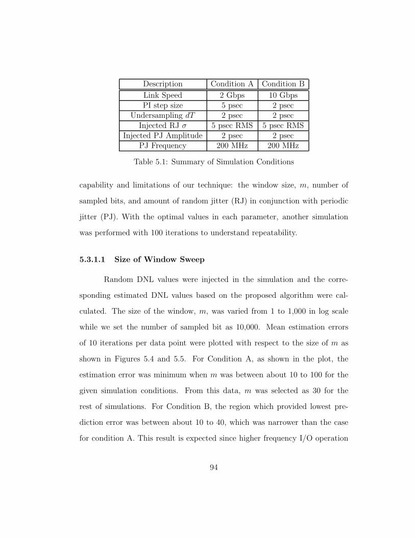
Description Condition A Condition B
Link Speed 2 Gbps 10 GbpsPI step size 5 psec 2 psec
Undersampling dT 2 psec 2 psecInjected RJ σ 5 psec RMS 5 psec RMS
Injected PJ Amplitude 2 psec 2 psecPJ Frequency 200 MHz 200 MHz
Table 5.1: Summary of Simulation Conditions
capability and limitations of our technique: the window size, m, number of
sampled bits, and amount of random jitter (RJ) in conjunction with periodic
jitter (PJ). With the optimal values in each parameter, another simulation
was performed with 100 iterations to understand repeatability.
5.3.1.1 Size of Window Sweep
Random DNL values were injected in the simulation and the corre-
sponding estimated DNL values based on the proposed algorithm were cal-
culated. The size of the window, m, was varied from 1 to 1,000 in log scale
while we set the number of sampled bit as 10,000. Mean estimation errors
of 10 iterations per data point were plotted with respect to the size of m as
shown in Figures 5.4 and 5.5. For Condition A, as shown in the plot, the
estimation error was minimum when m was between about 10 to 100 for the
given simulation conditions. From this data, m was selected as 30 for the
rest of simulations. For Condition B, the region which provided lowest pre-
diction error was between about 10 to 40, which was narrower than the case
for condition A. This result is expected since higher frequency I/O operation
94

100
101
102
103
0
5
10
15
20
25
30
Window Size (m)
Pre
dic
tio
n E
rro
r (L
SB
)
Figure 5.4: Estimation Error vs. Size of Window (Condition A)
decreases signal eye width which makes the signal more susceptible to aliased
jitter. m = 20 was selected to obtain minimum prediction error for Condition
B.
5.3.1.2 Number of Samples Sweep
In this simulation, the number of transmitted bits was varied from
100 to 10,000 to determine the dependency on the number of samples. For
each iteration of the simulation, a DNL value was randomly generated, and
then an estimated DNL was calculated using each algorithm. 20 iterations
per each number of samples were made to obtain stable results. Figures 5.6
and 5.7 present the estimation error for each data point of the number of bits.
95

100
101
102
103
0
5
10
15
20
25
30
Window Size (m)
Pre
dic
tio
n E
rro
r (L
SB
)
Figure 5.5: Estimation Error vs. Size of Window (Condition B)
Tables 5.2 and 5.3 summarize the data. In general, both algorithms showed
that the accuracy greatly increased once more than 1,000 bits were sampled.
For Condition B, prediction errors of the undersampling method were greater
than the ones for Condition A. Prediction errors of the sliding window search
based method were slightly increased for Condition B as compared to the ones
for Condition A. The proposed method based on the sliding window search
algorithm yielded better accuracy as compared to the plain undersampling
method in both conditions.
96
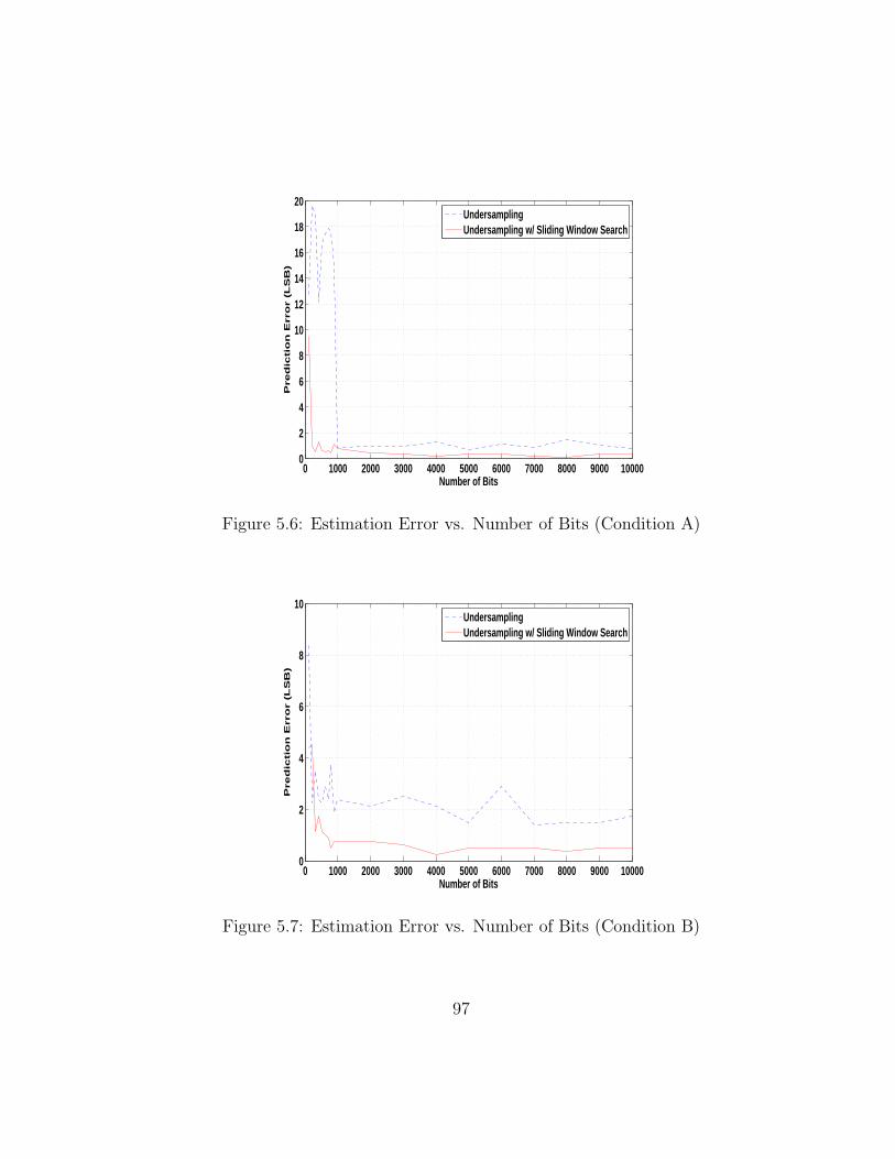
0 1000 2000 3000 4000 5000 6000 7000 8000 9000 100000
2
4
6
8
10
12
14
16
18
20
Number of Bits
Pre
dic
tio
n E
rro
r (L
SB
)
UndersamplingUndersampling w/ Sliding Window Search
Figure 5.6: Estimation Error vs. Number of Bits (Condition A)
0 1000 2000 3000 4000 5000 6000 7000 8000 9000 100000
2
4
6
8
10
Number of Bits
Pre
dic
tio
n E
rro
r (L
SB
)
UndersamplingUndersampling w/ Sliding Window Search
Figure 5.7: Estimation Error vs. Number of Bits (Condition B)
97

#Bits Undersampling w/ Sliding Window Search
100 12.75 9.5200 19.65 0.9300 18.9 0.5400 12.1 1.25500 16.65 0.6600 17.45 0.55700 17.85 0.6800 17.6 0.45900 15.1 1.1
1,000 0.85 0.82,000 0.95 0.453,000 0.9 0.354,000 1.25 0.25,000 0.7 0.36,000 1.1 0.37,000 0.85 0.28,000 1.45 0.19,000 1.05 0.310,000 0.8 0.3
Table 5.2: Estimation Error (LSB) vs. Number of Bits (Condition A)
98

#Bits Undersampling w/ Sliding Window Search
100 8.375 4.375200 2.25 4.5300 3.5 1.125400 2.375 1.75500 2.25 1.125600 2.875 1.0700 2.375 0.875800 3.75 0.5900 1.875 0.75
1,000 2.375 0.752,000 2.125 0.753,000 2.5 0.6254,000 2.125 0.255,000 1.5 0.56,000 2.875 0.57,000 1.375 0.58,000 1.5 0.3759,000 1.5 0.510,000 1.75 0.5
Table 5.3: Estimation Error (LSB) vs. Number of Bits (Condition B)
99

0 2 4 6 8 10 12 14 16 18 200
0.2
0.4
0.6
0.8
1
1.2
1.4
1.6
1.8
2
RJ RMS (psec)
Pre
dic
tio
n E
rro
r (L
SB
)
Undersampling
Undersampling w/ Sliding Window Search
Figure 5.8: Estimation Error vs. RJ σ (Condition A)
5.3.1.3 Amount of Jitter Sweep
In this simulation for Condition A, we set the amplitude of PJ to 10
psec across the simulation data points and varied RJ from 1 psec to 20 psec,
which ensured to cover both PJ and RJ component dominant cases. 10,000
bits were sampled and 20 iterations were made to select reliable data points.
Figure 5.8 and Table 5.4 present the results. Although there was a trend of
a slight increase of estimation errors when RJ was increased, the proposed
algorithm again showed better accuracy as compared to the undersampling
only case.
For Condition B, we scaled the amplitude of PJ to 3 psec to inject
reasonable jitter amount with respect to the link speed. Then we varied RJ
100

RJ RMS (psec) Undersampling w/ Sliding Window Search
1 0.4 0.12 0.65 0.13 0.65 0.14 0.65 0.25 1.25 0.26 0.7 0.27 0.9 0.158 1.25 0.39 0.7 0.110 1.3 0.311 1.05 0.312 1.3 0.313 1.3 0.214 1.25 0.5515 1.2 0.516 1.4 0.417 1.35 0.2518 1.85 0.319 1.3 0.4520 1.45 0.25
Table 5.4: Estimation Error (LSB) vs. RJ σ (Condition A)
101

0 2 4 6 8 10 12 14 16 18 200
1
2
3
4
5
RJ RMS (psec)
Pre
dic
tio
n E
rro
r (L
SB
)
UndersamplingUndersampling w/ Sliding Window Search
Figure 5.9: Estimation Error vs. RJ σ (Condition B)
from 1 psec to 20 psec. The same number of bits were sampled and 20 iterations
were made to select reliable data points. The results are presented in Figure 5.9
and Table 5.5. In addition to the fact that there is a general trend of the
sliding window search yielding better accuracy, the prediction errors for the
undersampling method were larger than the ones for Condition A.
5.3.1.4 Repeatability Analysis
With the given simulation conditions, we ran the simulation 100 times
to observe the repeatability of our method. Randomly generated DNL values
were injected and corresponding estimated DNLs based on each algorithm were
plotted to determine the repeatability. 10,000 bits were sampled to estimate
102

RJ RMS (psec) Undersampling w/ Sliding Window Search
1 1.0 1.02 1.0 1.1253 1.125 1.04 1.625 0.55 2.375 0.56 2.625 0.57 1.0 0.58 2.5 0.59 3.5 0.37510 2.25 0.87511 1.75 0.7512 4.25 0.513 2.25 0.7514 3.875 0.515 3.625 0.7516 2.125 1.12517 1.875 1.018 3.75 1.62519 3.375 2.520 3.25 2.125
Table 5.5: Estimation Error (LSB) vs. RJ σ (Condition B)
103

0 5 10 15 20 25 30 350
10
20
30
40
50
60
Injected DNL (LSB)
Pre
dic
ted
DN
L (
LS
B)
UndersamplingUndersampling w/ Sliding Window Search linear
Figure 5.10: Estimated DNL vs. Injected DNL (Condition A)
the DNLs. Figures 5.10 and 5.11 present the comparison between the plain
undersampling method and our sliding window search algorithm based method
for 2 Gbps and 10 Gbps links, respectively. More outliers were observed in
the plain undersampling method as compared to the proposed method, since
our method reduces the aliasing impact of injected jitters. Mean of DNL
estimation errors and standard deviation (STD) of the errors are summarized
in Tables 5.6 and 5.7. The results suggest that the sliding window search
algorithm is more repeatable as compared to the plain undersampling method.
Note that both mean error and STD of the errors were slightly increased in
10 Gbps link as compared to the ones for 2 Gbps link.
104

w/ SlidingUndersampling Window Search
DNL Mean Error 4.90 0.226DNL Error STD 14.79 0.20
Table 5.6: Repeatability Analysis Results (LSB) (Condition A)
0 2 4 6 8 10 12 14 160
5
10
15
20
25
30
35
Injected DNL (LSB)
Pre
dic
ted
DN
L (
LS
B)
UndersamplingUndersampling with Sliding Window Search linear
Figure 5.11: Estimated DNL vs. Injected DNL (Condition B)
w/ SlidingUndersampling Window Search
DNL Mean Error 3.918 0.528DNL Error STD 4.132 0.353
Table 5.7: Repeatability Analysis Results (LSB) (Condition B)
105

5.3.2 Hardware Validation
Hardware measurement using the proposed method was performed us-
ing silicon with a 1.25 Gbps serial link circuit. The serial link was implemented
with a PI based clock and data recovery (CDR) circuit which had 32 pro-
grammable PI steps. A design for testability (DFT) feature was implemented
to enable the proposed technique.
The general HVM test configuration for the serial link was based on the
loopback test scheme in that the TX output is connected to the RX input to
enable the timing margining based loopback. During the PI test mode, multi-
plexers and test mode signals reconfigured the PI based CDR circuitry to have
a proper undersampling setup, which is conceptually depicted in Figure 5.3.
Test content was developed using the proposed technique in a low cost
production tester environment. The ATE configuration included a standard
digital module that supports up to 667 Mbps input data rate and 500 Mbps
output sampling rate for general production test purposes. An arbitrary wave-
form generator (AWG) was installed to enable the proposed technique by driv-
ing a proper clock signal with the period of T + dT into the DUT. Figure 5.12
illustrates the hardware validation environment. The sampler circuit was im-
plemented in a way that it operates in high speed and latches 1 if the input
voltage is more than the threshold voltage, which is considered as the signal
transition voltage. The digital module denoted as ‘DM’ was connected to gen-
eral purpose I/Os (GPIOs) as well as the output of the sampler. The AWG
drove the undersampling clock for the sampler. When creating the undersam-
106
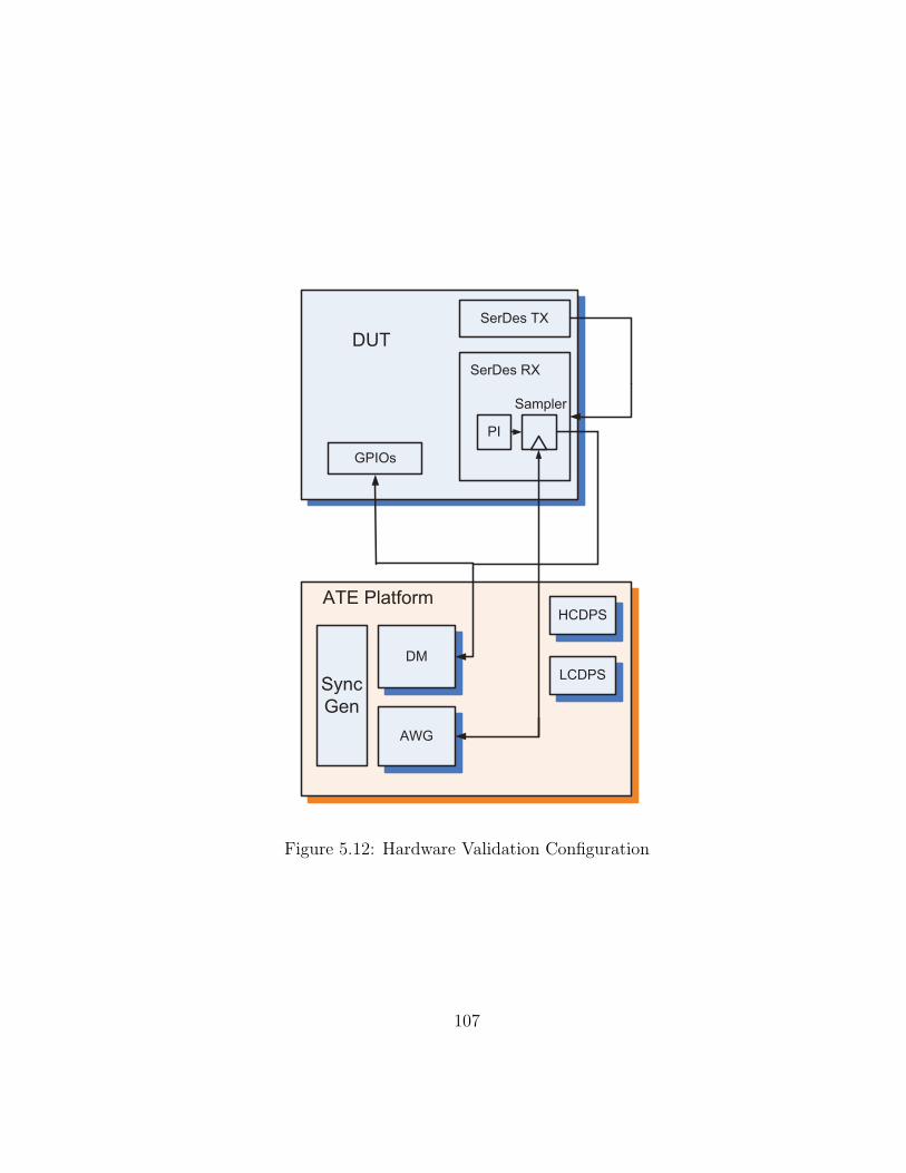
ATE Platform
DM
AWG
HCDPS
LCDPS
DUT
GPIOs
SerDes TX
PI
SerDes RX
Sampler
Sync
Gen
Figure 5.12: Hardware Validation Configuration
107

Pattern
xxx
xxx
xxx
SNDC 1
xxx
A:
xxx
JECH A
xxx
xxx
xxx
.
.
.
EXIT
xxx
PG#1
Pattern
xxx
xxx
xxx
A:
xxx
JECH A
xxx
xxx
xxx
.
.
.
EXIT
xxx
PG#2
Test Pgm:
C++ code;
C++ code;
C++ code;
.
.
executePattern();
C++ code;
.
.
Callback {
C++ code;
C++ code;
.
.
.
restartPattern();
}
(a)
(b)
(b)
(c)
(d)
(d)
(e)(e)
Figure 5.13: Tester Pattern and Test Program Synchronization
pling clock waveform, up to 5th harmonics were used to generate a low jitter
square waveform. Clock domains between two modules were synchronized by
a sync generation module.
In order to develop tester patterns that fit in pattern memory require-
ments and properly synchronize the digital module with the AWG, the fol-
lowing pattern and test program handshaking architecture was proposed as
illustrated in Figure 5.13. Each module had its own pattern generator which
is denoted as PG#1 or PG#2. The actual sequence is enumerated from (a)
108

through (e). The test program which was implemented in C++ had an initial-
ization code that was executed at the beginning of the test (a). The ‘execute
pattern’ function in the test program invoked patterns in both domains and ran
pre-conditioning patterns to enable the test mode on the DUT (b). A call back
function (c) was introduced to handle tasks such as tester conditioning and
initial result comparison that needed to be executed after the pre-conditioning
patterns. While the call back function was being executed the pattern from
PG#2 was running in an infinite loop to wait for the call back function to
complete. The call back function contained a ‘pattern restart’ function (d)
that properly synchronized the two domains again to collect undersampled bit
stream. The undersampled bit stream from the DUT was stored in vector
memory and after the patterns were executed, it returned to the test program
to post-process the data to extract the PI step edge location (e). The pro-
gram repeated the sequence to construct the full PI step edge locations and
extracted DNLs and INLs. Note that for the hardware validation, the reso-
lution interpolation technique was not implemented to create a simpler test
program.
At a nominal device supply voltage and room temperature condition,
we performed 12 measurements on 1 DUT and plotted the PI step edge lo-
cations. A normalized graph with respect to the 32 locations is described in
Figure 5.14. As shown in the figure, depending on the initial starting point
of the undersampling, the estimated PI step location starts from a different
location and the value wrap around when it reaches the maximum value. This
109

Figure 5.14: PI Step Location Plot for 32 Positions
fact does not impact the stability of our algorithm, since DNL values are cal-
culated based on differential values of the locations. For the cases where the
edge location values were wrapped around, proper handling was implemented
to yield correct DNL and subsequently INL estimations.
After collecting the 12 measurements, measured values were averaged
to calculate the final DNLs and INLs for the device. The same sequence was
repeated on 4 DUTs. The initial data collection on 4 DUTs suggested that
the synchronization delay induced between ATE’s dual pattern generation op-
eration and AWG instrument clock degraded the accuracy of the linearity
test technique. By characterizing the offset delta induced by this delay and
110

DUT ID A B C D
DNL Max Error 0.21 0.57 0.35 0.47INL Max Error 2.90 1.16 0.89 0.66DNL Error STD 0.16 0.24 0.20 0.17INL Error STD 0.94 0.51 0.61 0.48
Table 5.8: Hardware Validation Results (LSB)
properly compensating the measured data by applying the offset, we obtained
repeatable results which are summarized in Table 5.8 in a normalized man-
ner. The hardware measurement results were within reasonable error margin
as compared to 2 Gbps simulation results considering a slight difference on
simulation condition and speed.
Correlation activities were performed between system and tester result
outliers. A few DUTs randomly failed when the proposed method was used
in an HVM tester, although the same parts showed good linearities on a sys-
tem board. The failure was observed as an abrupt jump of the calculated
PI step location values for certain PI steps. Although the effort to minimize
the configuration difference between the system board and the tester such as
matching the board termination resistance did not yield the positive results,
experiments showed that increasing the common mode voltage for the under-
sampling clock signal improved the correlation results. Further investigation
identified that instrument noise from the tester pin electronics as well as the
AWG degraded signal integrity of the undersampling clock and the resultant
clock signal was marginal for certain DUTs in a random manner. Increasing
common mode voltage improved signal to noise ratio (SNR) of the undersam-
111

Before After
DNL Error 18.97 0.09INL Error 53.48 0.20
Table 5.9: Before & After Voltage Correction Results (LSB)
pling clock signal and resulted in elimination of the phase divergence issue.
Table 5.9 summarizes the difference between outlier results and corrected re-
sults after increasing the common mode voltage.
5.4 Comparison with RJ Injection Based PI Test Method
Table 5.10 summarizes the comparison between the RJ injection based
PI test method presented in the previous chapter and the sliding window
search based PI test method. In order to present fair comparison, simulation
results for 10 Gbps high speed I/O configuration are compared. 3σ based
maximum prediction error calculation results in 0.67 LSB for the RJ injection
based method and 1.58 LSB for the sliding window search based method. In
general, maximum prediction error is the most important factor to consider
when adopting certain method, since that the mean prediction errors can be
compensated by characterizing the measurement, and then applying offset
in real HVM test environment. With this consideration, RJ injection based
method is a more desirable method in terms of the test accuracy. However, the
sliding window search algorithm based method does not require a RJ injection
source on the load board which provides simpler and more cost effective test
solution. Users should consider the tradeoff between accuracy and cost to
112

RJ Injection Sliding Window Search
Mean DNL Error 0.31 LSB 0.53 LSBError STD 0.12 LSB 0.35 LSBMax Error 0.67 LSB 1.58 LSB
Tested Freq. 10 Gbps 10 GbpsArea Overhead Not significant Not significant
Additional RJ injection RJ injectionEquipment source required source not required
Table 5.10: Comparison between Two PI Test Methods
determine the optimum PI test solution for the application.
5.5 Summary
In this chapter, a cost effective phase interpolator test technique is
proposed. We demonstrate that the proposed method yields accurate mea-
surement results in both simulation and HVM ATE environment. The results
based on hardware validation show good correlation with actual system PI
characteristics as well as good repeatability. The proposed nonlinearity esti-
mation algorithm is efficient and concise in that it can be implemented in a
conventional HVM tester.
113

Chapter 6
Conclusions and Future Research Directions
6.1 Conclusions
In this dissertation, novel test methodologies are proposed which pro-
vide additional coverage on loopback test issues. The known limitations of
loopback test such as fault masking and non-ideality of margining circuitry
issues are discussed and three solutions are proposed to resolve the current
limitations.
The fault masking issue is addressed using the proposed methodology
in Chapter 3 to test the linearity of embedded ADCs and DACs in high speed
serial I/Os. It uses a loopback setup with additional Gaussian noise on the
loopback path, which distorts the code probability distribution of ADC. The
distortion was post-processed using the proposed algorithm to calculate the
nonlinearity of the ADC independent of DAC. Then, using the combined loop-
back response and the ADC’s individual response, the nonlinearity of DAC is
extracted. This procedure provides accurate DNLs and INLs of each con-
verter regardless of fault masking effect. Other than interconnection and test
mode switches which may already be available due to the existing loopback
configuration, no additional circuits are necessary as compared to other BIST
114

schemes. Since the proposed method is an algorithm based approach, it does
not depend on specific architectures of data converters in high speed I/Os.
Compared to testing with automated test equipment (ATE) or other BIST
circuitry, this approach is cost effective and is easy to implement.
The non-ideality issue of margining circuit is addressed using the pro-
posed test technique in Chapter 4 for phase interpolators using random jitter
injection. Using a random jitter source that generates a jitter in Gaussian
distribution, the bit probability distribution generated by the receiver is used
as reference. When generating the reference distribution, undersampling tech-
nique is used to construct an ideal distribution for the case when non-ideality
does not exist for the margining circuitry. Then, a phase interpolator is used
to create another set of distribution to be compared with the reference. The
difference between two distributions provide information to extract nonlinear-
ities of the phase interpolator. The proposed algorithm is cost effective in that
it does not require hardware overhead in the case of forwarded clock scheme.
For the derived clock scheme, we only need to implement one multiplexer in
the clock lane to implement clock injection capability. The load board or sys-
tem board only needs to contain a random jitter injector and a clock generator
for undersampling purpose. The proposed algorithm based on statistical data
collection and curve fitting scheme accurately predicts the DNL of the phase
interpolator. Experimental results show that our method accurately predicted
nonlinearities of the PI. Since our method does not require significant circuit
changes, it can be easily applied to various high speed I/O microarchitectures
115
where phase interpolators are used.
Although the proposed technique to extract non-ideality of phase in-
terpolators accurately estimates DNLs, it requires random jitter source on the
load board which may not be always available in a certain HVM test environ-
ment. Another PI linearity test technique described in Chapter 5 is proposed
to mitigate the requirement for the random jitter source using the proposed
sliding window search algorithm. Rather than using the random jitter source
on the load board, it uses intrinsic jitter profile collected from undersampling.
Instead of aggregating the entire bit stream to create the jitter distribution, it
calculates the edge transition location based on individual transition region to
avoid low frequency jitter aliasing effect. The sliding window search algorithm
is proposed to simplify the calculation while maintaining the accuracy of in-
dividual calculation of edge transition regions. The new algorithm accurately
estimates linearities and the method was implemented in a low cost HVM ATE
environment to assess the feasibility. The results based on hardware valida-
tion show good correlation with actual system PI characteristic as well as good
repeatability. The proposed nonlinearity estimation algorithm is efficient and
concise in that it can be implemented in a conventional HVM tester.
6.2 Future Research Directions
Overall, this dissertation addresses key limitations in loopback test by
proposing loopback compatible test methods to provide coverage on areas of
concern. As conclusions of the dissertation are discussed, high speed interface
116

test challenges will continue to grow with ever increasing speed and perfor-
mance. Some potential areas for future research direction are highlighted as
follows.
• The proposed sliding window search algorithm was validated on a hand-
ful of DUTs, further validation will be performed to evaluate the method
on volume manufacturing environment. We will also evaluate the method
on next generation serial link schemes operating over 10 Gbps, which
would provide a new set of challenges.
• As the speed of SerDes increases, it increases the size of the I/O design
due to fine calibration requirements which are mostly achieved by digital
logics. Although there is prior work on automated test pattern genera-
tion (ATPG) on various mixed signal blocks [9], methods to develop test
patterns automatically on high speed mixed signal IP blocks are not well
defined partly due to lack of widely adopted analog fault model. Devel-
opment of widely adopted analog fault models and novel technique that
can generate effective test patterns automatically will augment current
test solutions on high speed I/Os.
• Adaptive equalization function is being implemented in modern high
speed serial interface to overcome the channel bandwidth limitation.
There are previous papers [26, 45, 64] on the topic of the adaptive equal-
izer test. However, with ever increasing data rate on high speed serial
117

interface, the equalization circuitry will be more complex and sophis-
ticated, and hence the test will take long test time. Continuation of
research investment on the adaptive equalization test would provide so-
lutions to overcome many roadblocks in testing next generation high
speed I/O circuits.
• Since increasing number of building blocks requires digitally assisted
calibration, pre-silicon mixed signal verification is now an essential ver-
ification step in modern I/O IP design flow. Applying mixed signal
verification techniques to automate the fault grading and correlate the
pre-silicon test results with post silicon validation results would provide
added benefit by identifying effective test patterns and expediting turn
around time of the debug.
118

Bibliography
[1] DDR2 SDRAM Fully Buffered DIMMTM(FB-DIMMTM) design specifi-
cation. http://www.jedec.org/.
[2] HyperTransportTMI/O link specification revision 1. http://www.hypertransport.org.
[3] Introduction to XAUITM. http://www.10gea.org/.
[4] OC800TM user manual. Apria Technology.
[5] PCI ExpressTMbase specification. http://www.pcisig.com.
[6] T2000TM250Mhz digital module product description. Advantest Corpo-
ration.
[7] IEEE 802 10GBASE-T tutorial. http://ieee802.org/, 2003.
[8] Test and test equipment. The International Technology Roadmap For
Semiconductors, 2009.
[9] M. Abbas, K.-T. Cheng, Y. Furukawa, S. Komatsu, and K. Asada.
An automatic test generation framework for digitally-assisted adaptive
equalizers in high-speed serial links. In Design, Automation Test in
Europe Conference Exhibition (DATE), 2010, pages 1755 –1760, Mar.
2010.
119

[10] S. Aouini and G.W. Roberts. A predictable robust fully programmable
analog gaussian noise source for mixed-signal/digital ATE. In Test Con-
ference, 2006. ITC ’06. IEEE International, pages 1–10, Oct. 2006.
[11] M. Aoyama, K. Ogasawara, M. Sugawara, T. Ishibashi, S. Shimoyama,
K. Yamaguchi, T. Yanagita, and T. Noma. 3 Gbps, 5000 ppm spread
spectrum SerDes PHY with frequency tracking phase interpolator for
serial ATA. In VLSI Circuits, 2003. Digest of Technical Papers. 2003
Symposium on, pages 107–110, Jun. 2003.
[12] K. Arabi and B. Kaminska. Efficient and accurate testing of analog-to-
digital converters using oscillation-test method. In Proc. of European
Design and Test Conference, pages 348–352, 1997.
[13] K. Arabi, B. Kaminska, and J. Rzeszut. A new built-in self-test ap-
proach for digital-to-analog and analog-to-digital converters. In Proc.
of International Conference on Computer Aided Design, pages 491–494,
1994.
[14] K. Arabi, B. Kaminska, and J. Rzeszut. BIST for D/A and A/D con-
verters. In IEEE Design and Test of Computers, volume 13, pages
40–49, 1996.
[15] F. Azais, S. Bernard, Y. Bertrand, and M. Renovell. Towards an ADC
BIST scheme using the histogram test technique. In Proc. of IEEE
European Test Workshop, pages 53–58, 2000.
120
[16] F. Azais, S. Bernard, Y. Bertrand, and M. Renovell. Implementation
of a linear histogram BIST for ADCs. In Proc. of the 2001 Design,
Automation and Test in Europe Conference, pages 590–595, 2001.
[17] M. Benyahia, J.B. Moulard, F. Badets, A. Mestassi, T. Finateu, L. Vogt,
and F. Boissieres. A digitally controlled 5 GHz analog phase interpolator
with 10 GHz LC PLL. In Design and Technology of Integrated Systems
in Nanoscale Era, 2007. DTIS. International Conference on, pages 130–
135, Sep. 2007.
[18] J.F. Bulzacchelli, M. Meghelli, S.V. Rylov, W. Rhee, A.V. Rylyakov,
H.A. Ainspan, B.D. Parker, M.P. Beakes, Aichin Chung, T.J. Beukema,
P.K. Pepeljugoski, L. Shan, Y.H. Kwark, S. Gowda, and D.J. Friedman.
A 10-Gb/s 5-Tap DFE/4-Tap FFE transceiver in 90-nm CMOS tech-
nology. Solid-State Circuits, IEEE Journal of, 41(12):2885–2900, Dec.
2006.
[19] M. Burns and G. W. Roberts. An Introduction to Mixed-Signal IC Test
and Measurement. Oxford University Press, New York, NY, 2001.
[20] Y. Cai, B. Laquai, and K. Luehman. Jitter testing for gigabit serial
communication transceivers. IEEE Design and Test of Computers,
19(1):66–74, 2002.
[21] Y. Cai, S.A. Werner, G.J. Zhang, M.J. Olsen, and R.D. Brink. Jit-
ter testing for multi-gigabit backplane serdes ” techniques to decompose
121

and combine various types of jitter. In Proceedings of the 2002 IEEE In-
ternational Test Conference, ITC ’02, pages 700–709, Washington, DC,
USA, 2002. IEEE Computer Society.
[22] A.H. Chan and G.W. Roberts. A jitter characterization system using a
component-invariant vernier delay line. IEEE Trans. Very Large Scale
Integr. Syst., 12(1):79–95, 2004.
[23] H.-M. Chang, C.-H. Chen, K.-Y. Lin, and K.-T. Cheng. Calibration and
testing time reduction techniques for a digitally-calibrated pipelined adc.
In VLSI Test Symposium, 2009. VTS ’09. 27th IEEE, pages 291 –296,
May 2009.
[24] H.-M. Chang, M.-S. Lin, and K.-T. Cheng. Digitally-assisted analog/rf
testing for mixed-signal socs. In Asian Test Symposium, 2008. ATS
’08. 17th, pages 43 –48, Nov. 2008.
[25] A. Chatterjee and N. Nagi. Design for testability and built-in self-test
of mixed-signal circuits: a tutorial. In VLSI Design, 1997. Proceedings.,
Tenth International Conference on, pages 388–392, Jan. 1997.
[26] K.-T. Cheng and H.-M. Chang. Test strategies for adaptive equalizers.
In Custom Integrated Circuits Conference, 2009. CICC ’09. IEEE, pages
597 –604, Sep. 2009.
[27] J.H. Chun, H.Yu, and J.A. Abraham. An efficient linearity test for on-
chip high speed ADC and DAC using loop-back. In ACM Great Lakes
122

Symposium on VLSI, pages 328–331, 2004.
[28] J.H. Chun, J.W. Lee, and J.A. Abraham. A novel characterization tech-
nique for high speed I/O mixed signal circuit components using random
jitter injection. In Proceedings of the 2010 Asia and South Pacific De-
sign Automation Conference, ASPDAC ’10, pages 312–317, Piscataway,
NJ, USA, 2010. IEEE Press.
[29] W. Dalal and D.A. Rosenthal. Measuring jitter of high speed data
channels using undersampling techniques. In Proceedings of the 1998
IEEE International Test Conference, ITC ’98, pages 814–818, Washing-
ton, DC, USA, 1998. IEEE Computer Society.
[30] P. Dierckx. Curve and surface fitting with splines. Oxford University
Press, Inc., New York, NY, USA, 1993.
[31] P. Dudek, S. Szczepanski, and J.V. Hatfield. A high-resolution cmos
time-to-digital converter utilizing a vernier delay line. Solid-State Cir-
cuits, IEEE Journal of, 35(2):240 –247, Feb. 2000.
[32] D.J. Foley and M.P. Flynn. A low-power 8-pam serial transceiver in 0.5-
um digital cmos. IEEE Journal of Solid-State Circuits, 37(3):310–316,
2002.
[33] W.A. Fritzsche and A.E. Haque. Low cost testing of multi-GBit device
pins with ATE assisted loopback instrument. In Test Conference, 2008.
ITC 2008. IEEE International, pages 1–8, Oct. 2008.
123

[34] T. Fujibe, M. Suda, K. Yamamoto, Y. Nagata, K. Fujita, D. Watanabe,
and T. Okayasu. Dynamic arbitrary jitter injection method for ¡ 6.5Gb/s
SerDes testing. In Test Conference, 2009. ITC 2009. International,
pages 1–10, Nov. 2009.
[35] S. Goyal and A. Chatterjee. Linearity testing of A/D converters using
selective code measurement. J. Electron. Test., 24:567–576, Dec. 2008.
[36] S. Goyal and M. Purtell. Alternate test methodology for high speed
A/D converter testing on low cost tester. In Test Symposium, 2005.
Proceedings. 14th Asian, pages 14 – 17, Dec. 2005.
[37] A. Haider, S. Bhattacharya, G. Srinivasan, and A. Chatterjee. A system-
level alternate test approach for specification test of RF transceivers in
loopback mode. In VLSI Design, 2005. 18th International Conference
on, pages 289 – 294, Jan. 2005.
[38] H. Higashi, S. Masaki, M. Kibune, S. Matsubara, T. Chiba, Y. Doi,
H. Yamaguchi, H. Takauchi, H. Ishida, K. Gotoh, and H. Tamura. A
5-6.4-Gb/s 12-channel transceiver with pre-emphasis and equalization.
Solid-State Circuits, IEEE Journal of, 40(4):978 – 985, Apr. 2005.
[39] W.T. Holman, J.A. Connelly, and A.B. Dowlatabadi. An integrated
analog/digital random noise source. Circuits and Systems I: Funda-
mental Theory and Applications, IEEE Transactions on, 44(6):521–528,
Jun. 1997.
124

[40] D. Hong and K.-T. Cheng. Bit error rate estimation for improving jitter
testing of high-speed serial links. In Test Conference, 2006. ITC ’06.
IEEE International, pages 1 –10, Oct. 2006.
[41] D. Hong and K.-T. Cheng. Bit-error rate estimation for bang-bang
clock and data recovery circuit in high-speed serial links. In VLSI Test
Symposium, 2008. VTS 2008. 26th IEEE, pages 17 –22, May 2008.
[42] D. Hong, C. Dryden, and G. Saksena. An efficient random jitter mea-
surement technique using fast comparator sampling. In Proceedings
of the 23rd IEEE Symposium on VLSI Test, VTS ’05, pages 123–130,
Washington, DC, USA, 2005. IEEE Computer Society.
[43] D. Hong, C.-K. Ong, and K.-T. Cheng. BER estimation for serial
links based on jitter spectrum and clock recovery characteristics. In
Proceedings of the International Test Conference on International Test
Conference, ITC ’04, pages 1138–1147, Washington, DC, USA, 2004.
IEEE Computer Society.
[44] D. Hong, C.-K. Ong, and K.-T. Cheng. Bit-error-rate estimation for
high-speed serial links. Circuits and Systems I: Regular Papers, IEEE
Transactions on, 53(12):2616 –2627, Dec. 2006.
[45] D. Hong, S. Saberi, K.-T. Cheng, and C.P. Yue. A two-tone test method
for continuous-time adaptive equalizers. In Design, Automation Test in
Europe Conference Exhibition, 2007. DATE ’07, pages 1 –6, Apr. 2007.
125

[46] J.-L. Huang and K.-T. Cheng. An on-chip short-time interval measure-
ment technique for testing high-speed communication links. In Proceed-
ings of the 19th IEEE VLSI Test Symposium, VTS ’01, pages 380–385,
Washington, DC, USA, 2001. IEEE Computer Society.
[47] J.-L. Huang, C.-K. Ong, and K.-T. Cheng. A BIST scheme for on-chip
ADC and DAC testing. In Proc. of the 2000 Design, Automation and
Test in Europe Conference and Exhibition, pages 216–220, 2000.
[48] P. Iyer, S. Jain, B. Casper, and J. Howard. Testing high-speed io
links using on-die circuitry. In VLSI Design, 2006. Held jointly with
5th International Conference on Embedded Systems and Design., 19th
International Conference on, pages 4–10, Jan. 2006.
[49] Y. Jiang and A. Piovaccari. A compact phase interpolator for 3.125G
SerDes application. In Mixed-Signal Design, 2003. Southwest Sympo-
sium on, pages 249–252, Feb. 2003.
[50] L. Jin. Linearity test time reduction for analog-to-digital converters
using the kalman filter with experimental parameter estimation. In
Test Conference, 2008. ITC 2008. IEEE International, pages 1 –8, Oct.
2008.
[51] L. Jin, K. Parthasarathy, T. Kuyel, D. Chen, and R.L. Geiger. Ac-
curate testing of analog-to-digital converters using low linearity signals
with stimulus error identification and removal. Instrumentation and
Measurement, IEEE Transactions on, 54(3):1188 – 1199, Jun. 2005.
126

[52] D. A. Johns and K. Martin. Analog Integrated Circuit Design. John
Wiley and Sons, Inc., 1997.
[53] D.C. Keezer, D. Minier, and P. Ducharme. Variable delay of multi-
gigahertz digital signals for deskew and jitter-injection test applications.
In Design, Automation and Test in Europe, 2008. DATE ’08, pages 1486
–1491, Mar. 2008.
[54] B. Kim and J.A. Abraham. Efficient loopback test for aperture jitter
in embedded mixed-signal circuits. Circuits and Systems I: Regular
Papers, IEEE Transactions on, 58(8):1773 –1784, Aug. 2011.
[55] B. Kim, Z. Fu, and J.A. Abraham. Transformer-coupled loopback test
for differential mixed-signal specifications. In VLSI Test Symposium,
2007. 25th IEEE, pages 291 –296, May 2007.
[56] B. Kim, H. Shin, J.H. Chun, and J.A. Abraham. Predicting mixed-
signal dynamic performance using optimised signature-based alternate
test. Computers Digital Techniques, IET, 1(3):159 –169, May 2007.
[57] S. Kim and M. Soma. An all-digital built-in self-test for high-speed
phase-locked loops. Circuits and Systems II: Analog and Digital Signal
Processing, IEEE Transactions on, 48(2):141 –150, Feb. 2001.
[58] R. Kreienkamp, U. Langmann, C. Zimmermann, T. Aoyama, and H. Sied-
hoff. A 10-Gb/s CMOS clock and data recovery circuit with an analog
127

phase interpolator. Solid-State Circuits, IEEE Journal of, 40(3):736–
743, Mar. 2005.
[59] N. Kurd, J. Douglas, P. Mosalikanti, and R. Kumar. Next generation
IntelR© micro-architecture (nehalem) clocking architecture. In VLSI Cir-
cuits, 2008 IEEE Symposium on, pages 62–63, Jun. 2008.
[60] B. Laquai and Y. Cai. Testing gigabit multilane serdes interfaces with
passive jitter injection filters. In Test Conference, 2001. Proceedings.
International, pages 297 –304, 2001.
[61] J.W. Lee, J.H. Chun, and J.A. Abraham. A random jitter RMS estima-
tion technique for BIST applications. In Asian Test Symposium, 2009.
ATS ’09., pages 9 –14, Nov. 2009.
[62] J.W. Lee, J.H. Chun, and J.A. Abraham. A delay measurement method
using a shrinking clock signal. In ACM Great Lakes Symposium on
VLSI, pages 139–142, 2010.
[63] M. Li. Jitter, noise, and signal integrity at high-speed. Prentice Hall
Press, Upper Saddle River, NJ, USA, 2007.
[64] M. Lin and K.-T. Cheng. Testable design for adaptive linear equalizer
in high-speed serial links. In Test Conference, 2006. ITC ’06. IEEE
International, pages 1 –10, Oct. 2006.
[65] M. Lin, K.-T. Cheng, J. Hsu, M.C. Sun, J. Chen, and S. Lu. Production-
oriented interface testing for PCI-ExpressTMby enhanced loop-back tech-
128

nique. In Test Conference, 2005. Proceedings. ITC 2005. IEEE Inter-
national, pages 11–20, Nov. 2005.
[66] M. Mahoney. DSP-Based Testing of Analog and Mixed-Signal Circuits.
IEEE Computer Society Press, Washington, D.C., 1987.
[67] T.M. Mak, M. Tripp, and A. Meixner. Testing Gbps interfaces without
a gigahertz tester. IEEE Design and Test of Computers, 21(4):278–286,
2004.
[68] A. Martin, B. Casper, J. Kennedy, J. Jaussi, and R. Mooney. 8 Gb/s dif-
ferential simultaneous bidirectional link with 4mV 9ps waveform capture
diagnostic capability. In Solid-State Circuits Conference, 2003. Digest
of Technical Papers. ISSCC. 2003 IEEE International, pages 78–479
vol.1, 2003.
[69] S. Max. Ramp testing of ADC transition levels using finite resolution
ramps. In Proc. of the 2001 IEEE International Test Conference, pages
495–501, 2001.
[70] A. Meixner, A. Kakizawa, B. Provost, and S. Bedwani. External loop-
back testing experiences with high speed serial interfaces. In Test Con-
ference, 2008. ITC 2008. IEEE International, pages 1–10, Oct. 2008.
[71] M. J. Ohletz. Hybrid built in self test(HBIST) for mixed analogue/digital
ICs. In Proc. of the 1993 IEEE International Test Conference, pages
307–316, 1993.
129

[72] V. G. Oklobdzija and R. K. Krishnamurthy. High-Performance Energy-
Efficient Microprocessor Design (Series on Integrated Circuits and Sys-
tems). Springer-Verlag New York, Inc., Secaucus, NJ, USA, 2006.
[73] S. Ozev and A. Orailoglu. An integrated tool for analog test gener-
ation and fault simulation. In Proc. of the 2002 IEEE International
Symposium on Quality of Electronic Design, pages 267–272, 2002.
[74] J. Park, H. Shin, and J.A. Abraham. Pseudorandom test for nonlinear
circuits based on a simplified volterra series model. In ISQED, pages
495–500, 2007.
[75] J. Park, H. Shin, and J.A. Abraham. Parallel loopback test of mixed-
signal circuits. In VLSI Test Symposium, 2008. VTS 2008. 26th IEEE,
pages 309 –316, May 2008.
[76] J.G. Proakis. Digital Communications. McGraw Hill, 4th edition, 2001.
[77] B. Provost. Testability techniques for phase interpolators. In US Patent
Application no. 20090122849, 2009.
[78] A. Raghunathan, J.H. Chun, J.A. Abraham, and A. Chatterjee. Quasi-
oscillation based test for improved prediction of analog performance pa-
rameters. In Test Conference, 2004. Proceedings. ITC 2004. Interna-
tional, pages 252 – 261, Oct. 2004.
130

[79] A. Raghunathan, H. Shin, and J.A. Abraham. Prediction of analog per-
formance parameters using oscillation based test. In VLSI Test Sympo-
sium, 2004. Proceedings. 22nd IEEE, pages 377 – 382, Apr. 2004.
[80] M. Renovell, F. Azais, S. Bernard, and Y. Bertrand. Hardware resource
minimization for histogram-based ADC BIST. In Proc. of the 18th IEEE
VLSI Test Symposium, pages 247–252, 2000.
[81] I. Robertson, G. Hetherington, T. Leslie, I. Parulkar, and R. Lesnikoski.
Testing high-speed, large scale implementation of SerDes I/Os on chips
used in throughput computing systems. Test Conference, International,
0:8–17, 2005.
[82] J. Savoj and B. Razavi. A 10-Gb/s CMOS clock and data recovery
circuit with a half-rate linear phase detector. Solid-State Circuits, IEEE
Journal of, 36(5):761 –768, May 2001.
[83] X. Shi and F. Assaderaghi. Phase linearity test circuit. In US Patent
Application no. 20070252735, 2007.
[84] H. Shin, B. Kim, and J.A. Abraham. Spectral prediction for specification-
based loopback test of embedded mixed-signal circuits. In VLSI Test
Symposium, 2006. Proceedings. 24th IEEE, pages 1–6, May 2006.
[85] H. Shin, J. Park, and J.A. Abraham. A statistical digital equalizer for
loopback-based linearity test of data converters. In Test Symposium,
2006. ATS ’06. 15th Asian, pages 245 –250, Nov. 2006.
131

[86] M. Soma, W. Haileselassie, J. Yan, and R. Raina. A wavelet-based
timing parameter extraction method. In Test Conference, 2002. Pro-
ceedings. International, pages 120 – 128, 2002.
[87] R. Stephens. Jitter analysis: The dual-dirac model, RJ/DJ, and Q-
scale. Agilent Technologies, 2004.
[88] S. Sunter, C. McDonald, and G. Danialy. Contactless digital testing
of IC pin leakage currents. In Test Conference, 2001. Proceedings.
International, pages 204 –210, 2001.
[89] S. Sunter and N. Nagi. Test metrics for analog parametric faults. In
VLSI Test Symposium, 1999. Proceedings. 17th IEEE, pages 226 –234,
1999.
[90] S. Sunter and A. Roy. On-chip digital jitter measurement, from mega-
hertz to gigahertz. Design and Test of Computers, IEEE, 21(4):314–321,
Jul.-Aug. 2004.
[91] S. Sunter and A. Roy. A mixed-signal test bus and analog BIST with
’unlimited’ time and voltage resolution. In European Test Symposium
(ETS), 2011 16th IEEE, pages 81 –86, May 2011.
[92] S. Sunter, A. Roy, and J.-F. Cote. An automated, complete, structural
test solution for SerDes. In Test Conference, 2004. Proceedings. ITC
2004. International, pages 95 – 104, Oct. 2004.
132

[93] S. K. Sunter and N. Nagi. A simplified polynomial-fitting algorithm for
DAC and ADC BIST. In Proc. of International Test Conference, pages
389–395, 1997.
[94] S.K. Sunter. Testing high frequency ADCs and DACs with a low fre-
quency analog bus. In Test Conference, 2003. Proceedings. ITC 2003.
International, volume 1, pages 228 – 235, Oct. 2003.
[95] M. Suzuki, R. Shimizu, N. Naka, and K. Nakamura. High-speed inter-
face testing. Asian Test Symposium, 0:461, 2001.
[96] E. Teraoka and et al. A built-in self-test for ADC and DAC in a single-
chip speech CODEC. In Proc. of the IEEE International Test Confer-
ence, pages 791–796, 1993.
[97] Y. Tomita, M. Kibune, J. Ogawa, W.W. Walker, H. Tamura, and T. Kuroda.
A 10-Gb/s receiver with series equalizer and on-chip ISI monitor in 0.11-
mu;m CMOS. Solid-State Circuits, IEEE Journal of, 40(4):986 – 993,
Apr. 2005.
[98] M.F. Toner and G.W. Roberts. A BIST scheme for an SNR test of a
sigma-delta ADC. In Proc. of the 1993 IEEE International Test Con-
ference, pages 805–814, 1993.
[99] M. Tripp, T.M. Mak, and A. Meixner. Elimination of traditional func-
tional testing of interface timings at Intel. In Test Conference, 2004.
Proceedings. ITC 2004. International, pages 1448 – 1454, Oct. 2004.
133
[100] P.N. Variyam and A. Chatterjee. Specification-driven test generation
for analog circuits. Computer-Aided Design of Integrated Circuits and
Systems, IEEE Transactions on, 19(10):1189 –1201, Oct. 2000.
[101] M. F. Wagdy and M. Goff. Linearizing average transfer characteristics
of ideal ADC’s via analog and digital dither. IEEE Trans. on Instru-
mentation and Measurement, 43(2):146–150, 1994.
[102] N. Weste and D. Harris. CMOS VLSI Design: A Circuits and Systems
Perspective. Addison-Wesley Publishing Company, USA, 4th edition,
2010.
[103] C. L. Wey. Built-in self-test design of current-mode algorithmic analog-
to-digital converters. IEEE Trans. on Instrumentation and Measure-
ment, 46(3):667–671, 1997.
[104] T. Xia, H. Zheng, J. Li, and A. Ginawi. Self-refereed on-chip jitter mea-
surement circuit using vernier oscillators. In VLSI, 2005. Proceedings.
IEEE Computer Society Annual Symposium on, pages 218 – 223, May
2005.
[105] T.J. Yamaguchi, M. Soma, M. Ishida, T. Watanabe, and T. Ohmi. Ex-
traction of instantaneous and rms sinusoidal jitter using an analytic sig-
nal method. Circuits and Systems II: Analog and Digital Signal Pro-
cessing, IEEE Transactions on, 50(6):288 – 298, Jun. 2003.
134

[106] C.-K.K. Yang, V. Stojanovic, S. Modjtahedi, M.A. Horowitz, and W.F.
Ellersick. A serial-link transceiver based on 8-g samples/s A/D and
D/A converters in 0.25-um cmos. Solid-State Circuits, IEEE Journal
of, 36(11):1684–1692, Nov. 2001.
[107] J. Yang, J. Kim, S. Byun, C. Conroy, and B. Kim. A quad-channel
3.125Gb/s/ch serial-link transceiver with mixed-mode adaptive equalizer
in 0.18 um CMOS. In Solid-State Circuits Conference, 2004. Digest of
Technical Papers. ISSCC. 2004 IEEE International, pages 176 – 520
Vol.1, Feb. 2004.
[108] H. Yu, J.A. Abraham, S. Hwang, and J. Roh. Efficient loop-back testing
of on-chip ADCs and DACs. In Proc. of the Asia and South Pacific
Design Automation Conference, pages 651–656, 2003.
[109] H. Yu, S. Hwang, and J.A. Abraham. DSP-based statistical self test of
on-chip converters. In Proc. of the 21st IEEE VLSI Test Symposium,
pages 83–88, 2003.
[110] H. Yu, H. Shin, J.H. Chun, and J.A. Abraham. Performance charac-
terization of mixed-signal circuits using a ternary signal representation.
In Test Conference, 2004. Proceedings. ITC 2004. International, pages
1389 – 1397, Oct. 2004.
135

Vita
Ji Hwan Chun was born in Seoul, South Korea in 1977. He received the
Bachelor of Science degree in Electronic Engineering from Yonsei University,
Seoul, South Korea in 2001. After joining the University of Texas at Austin
for his graduate study, he received the Master of Science in Engineering de-
gree in Electrical and Computer Engineering from the University of Texas at
Austin in 2003. While continuing his Ph.D. study in part-time, he joined
Intel Corporation in 2004 where he has worked on design, pre-silicon verifica-
tion, and post-silicon tests for IntelR© PentiumR© 4, AtomTM, XeonR©, and HPC
class microprocessors. He is currently a Senior Component Design Engineer
specializing on Mixed Signal Verification and DFX (Design for Testability, De-
bug, Verification, and Manufacturing) for next generation high performance
CPUs. He is a recipient of University of Texas Microelectronics and Computer
Development (MCD) Fellowship in 2001-03.
Permanent address: 900 Pepper Tree Ln Apt 618Santa Clara, California 95051
This dissertation was typeset with LATEX† by the author.
†LATEX is a document preparation system developed by Leslie Lamport as a special
version of Donald Knuth’s TEX Program.
136