Embed Size (px)
Citation preview

i
CONTENTSChapter 1. Getting Started ................................................................................... 1-1
Mainboard Specifications .................................................................................. 1-2Mainboard Layout .............................................................................................. 1-4
Chapter 2. Hardware Setup ................................................................................. 2-1Quick Components Guide .................................................................................. 2-2CPU (Central Processing Unit) ........................................................................... 2-2
Introduction to LGA 775 CPU ..................................................................... 2-3CPU & Cooler Installation ............................................................................ 2-4
Memory ............................................................................................................... 2-7Installing DDRII Modules ............................................................................. 2-7
Power Supply ..................................................................................................... 2-8ATX 24-Pin Power Connector: ATX1 ......................................................... 2-8ATX 12V Power Connector: JPW1 ............................................................ 2-8
Back Panel .......................................................................................................... 2-9Connectors ....................................................................................................... 2-11
Floppy Disk Drive Connector: FDD1 ........................................................ 2-11ATA133 Hard Disk Connectors: IDE1 & IDE2 ........................................... 2-11Serial ATA Connectors: SATA1, SATA2 .................................................. 2-12BIOS Password Clear: JPWD1 ................................................................ 2-12Fan Power Connectors: CPU_FAN1, SYS_FAN1 ................................... 2-13Front USB Connectors: JUSB1, JUSB2 .................................................. 2-13SPDIF-Out Connector: SPDOUT1 ............................................................. 2-14Front Panel Audio Connector: JAUD1 ..................................................... 2-14BIOS Flash Write Protection: JWP1 ......................................................... 2-14IEEE 1394 Connectors: J1394_1 ............................................................. 2-15Front Panel Connectors: JFP1/JFP2 ........................................................ 2-15Clear CMOS Jumper: JBAT1 .................................................................... 2-16BIOS Recovery: JBR1 .............................................................................. 2-16
Jumpers ............................................................................................................ 2-16Slots .................................................................................................................. 2-17
PCI (Peripheral Component Interconnect) Express Slots ....................... 2-17PCI (Peripheral Component Interconnect) Slots ...................................... 2-17PCI Interrupt Request Routing .................................................................. 2-18
Chapter 3. BIOS Setup ........................................................................................... 3-1Entering Setup .................................................................................................... 3-2
Control Keys ............................................................................................... 3-3Getting Help ................................................................................................ 3-3
ii
General Help <F1> ...................................................................................... 3-3The Main Menu ................................................................................................... 3-4Standard CMOS Features .................................................................................. 3-6Advanced BIOS Features .................................................................................. 3-8Advanced Chipset Features ........................................................................... 3-10Integrated Peripherals ...................................................................................... 3-13Power Management Setup .............................................................................. 3-15PNP/PCI Configurations .................................................................................... 3-18H/W Monitor ...................................................................................................... 3-19Load Optimized Defaults .................................................................................. 3-20Set Supervisor/ User Password ..................................................................... 3-21
1-1
Getting Started
Getting StartedChapter 1
Thank you for choosing the MS-7293 Series (MS-7293v2.X) Micro ATX mainboard. The MS-7293 Seriesmainboards are based on VIA® PT890 & VIA® 8237Achipsets for optimal system efficiency. Designed to fitthe advanced Intel® Pentium 4 processor, themainboards deliver a high performance and profes-sional desktop platform solution.

MS-7293 Mainboard
1-2
Processor Support- Supports Intel® Pentium 4, Pentium D, Celeron D
and intel® CoreTM 2 Duo processors in the LGA775 package.- Supports 3/4 pin CPU Fan Pin-Header with Fan Speed Control.- Supports EIST Technology- Supports Hyper-Threading (HT) Technology- Supports Intel Dual Core Technology
Supported FSB- 533/800/1066 MHz
Chipset- North Bridge: VIA® PT890- South Bridge: VIA® 8237A
Memory Support- DDRII 400/533 SDRAM (2GB Max)- 2 DDRII DIMMs (240pin / 1.8V)
LAN- Supports LAN 10/100 Fast Ethermet by VIA® VT6103L
IEEE 1394- Chip integrated by VIA VT6308
Audio- Chip integrated by Realtek ALC888- Flexible 8-channel audio with jack sensing- Compliant with Azalia 1.x HD audio.
IDE- 2 ports (4 IDE channels).- Supports Ultra DMA 33/66/100/133 mode- Supports PIO, Bus Master operation mode
SATA- 2 SATA ports- Supports 2 SATA devices.- Supports storage and data transfers at up to 150 MB/s
Floppy- 1 floppy port- Supports 1 FDD with 360K, 720K, 1.2M, 1.44M and 2.88Mbytes
Mainboard Specifications

1-3
Getting Started
Connectors
Backpannel- 1 serial port (COM1)- 1 IEEE 1394 port- 4 USB 2.0 Ports- 1 LAN jack- 6 flexible audio jacks- 1 SPDIF Out connector
On-Board Pinheaders- 1 front Audio pinheader- 1 SPDIF-out pinheader- 1 IEEE 1394 pinheaders- 2 USB 2.0 pinheaders- 1 front panel pinheader (JFP1)
Slots- 1 PCI Express x16 slot- 1 PCI Express x1 slot- 2 PCI slots.- Support 3.3V/ 5V PCI bus Interface
Form Factor
- Micro-ATX (24.4cm X 24.4cm)
Mounting- 8 mounting holes
MS-7293 Mainboard
1-4
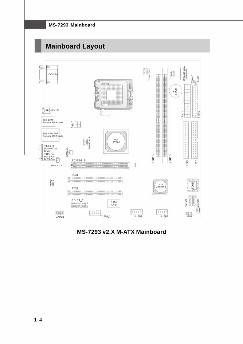
MS-7293 v2.X M-ATX Mainboard
Mainboard Layout
BATT+
BIO
SID
E 2
IDE 1
FDD
1
ATX 1
PCIE1_1
PCI2
PCI1
DIM
M1
DIM
M2PCIE16_1
SY
S_FA
N1
CP
U_FA
N1
JBAT
1
Winbond
W83627E
HG
JBR
1
JPW
D1
JUSB1J1394_1
SPDOUT1
JAUD1
Audio
Codec
VIA
VT6103L
JUSB2
SATA
1
SATA
2JW
P1
JFP1
JPW
1
Top: LAN JackBottom: USB ports
Top:1394Bottom: USB ports
T:M:B:
Line-InLine-OutMic
T:RS-OutM:CS-OutB:SS-Out
COM Port
SPDIFOUT1
VIAVT8237A
1394Chip
VIAPT890
2-1
Hardware Setup
Hardware SetupChapter 2
This chapter provides you with the information abouthardware setup procedures. While doing the installa-tion, be careful in holding the components and followthe installation procedures. For some components, ifyou install in the wrong orientation, the componentswill not work properly.
Use a grounded wrist strap before handling computercomponents. Static electricity may damage the compo-nents.

MS-7293 Mainboard
2-2
Quick Components Guide
DDRII DIMMs, p.2-7
Back PanelI/O, p.2-9
IDE1/2, p.2-12
ATX1, p.2-11
PCI Slots, p.2-17 SATA1/2,p.2-12
FDD1, p.2-11
SYS_FAN1, p.2-13
PCIE Slot, p.2-17
CPU, p.2-3
J1394_1, p.2-15 JFP1, p.2-15JAUD1, p.2-14
JPW1, p.2-8
JUSB1/2, p.2-13
SPDOUT1, p.2-14
JPWD1, p.2-12
PCIE Slot, p.2-17
CPU_FAN1, p.2-13
JBAT1, p.2-16
JBR1, p.2-16
JWP1, p.2-14

2-3
Hardware Setup
CPU (Central Processing Unit)
This mainboard supports Intel® Pentium 4 processor in LGA 775 package. When youare installing the CPU, make sure to install the cooler to prevent overheating.If you do not have the CPU cooler, contact your dealer to purchase and install thembefore turning on the computer.For the latest information about CPU, please visit http://www.msi.com.tw/program/products/mainboard/mbd/pro_mbd_cpu_support.php.
Important
1. Overheating will seriously damage the CPU and system. Always makesure the cooling fan can work properly to protect the CPU from overheat-ing.
2. Make sure that you apply an even layer of heat sink paste (or thermal tape)between the CPU and the heatsink to enhance heat dissipation.
3. While replacing the CPU, always turn off the ATX power supply or unplugthe power supply’s power cord from the grounded outlet first to ensure thesafety of CPU.
Introduction to LGA 775 CPUThe surface of LGA 775 CPU.Remember to apply some siliconeheat transfer compound on it forbetter heat dispersion.
Yellow triangle is the Pin 1 indicator
The pin-pad side of LGA 775CPU.
Yellow triangle is the Pin 1 indicator
Alignment Key Alignment Key

MS-7293 Mainboard
2-4
2. Remove the cap from lever hingeside (as the arrow shows).
1. The CPU has a plastic cap on it toprotect the contact from damage.Before you install the CPU, alwayscover it to protect the socket pin.
3. The pins of socket reveal.
CPU & Cooler InstallationWhen you are installing the CPU, make sure the CPU has a cooler at-
tached on the top to prevent overheating. If you do not have the cooler, contactyour dealer to purchase and install them before turning on the computer. Meanwhile,do not forget to apply some silicon heat transfer compound on CPU before installingthe heat sink/cooler fan for better heat dispersion.
Follow the steps below to install the CPU & cooler correctly. Wrong installationwill cause the damage of your CPU & mainboard.
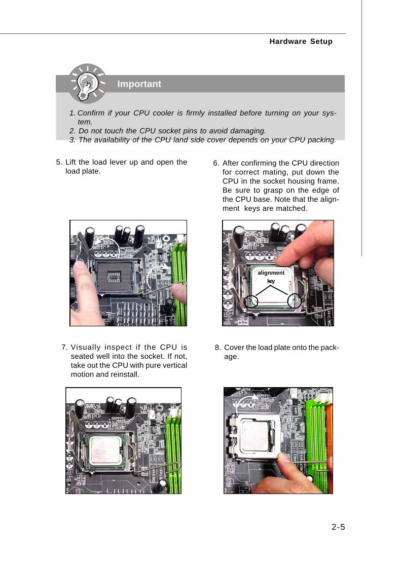
4. Open the load lever.
2-5
Hardware Setup
Important
1. Confirm if your CPU cooler is firmly installed before turning on your sys-tem.
2. Do not touch the CPU socket pins to avoid damaging.3. The availability of the CPU land side cover depends on your CPU packing.
6. After confirming the CPU directionfor correct mating, put down theCPU in the socket housing frame.Be sure to grasp on the edge ofthe CPU base. Note that the align-ment keys are matched.
8. Cover the load plate onto the pack-age.
7. Visually inspect if the CPU isseated well into the socket. If not,take out the CPU with pure verticalmotion and reinstall.
alignmentkey
5. Lift the load lever up and open theload plate.
MS-7293 Mainboard
2-6
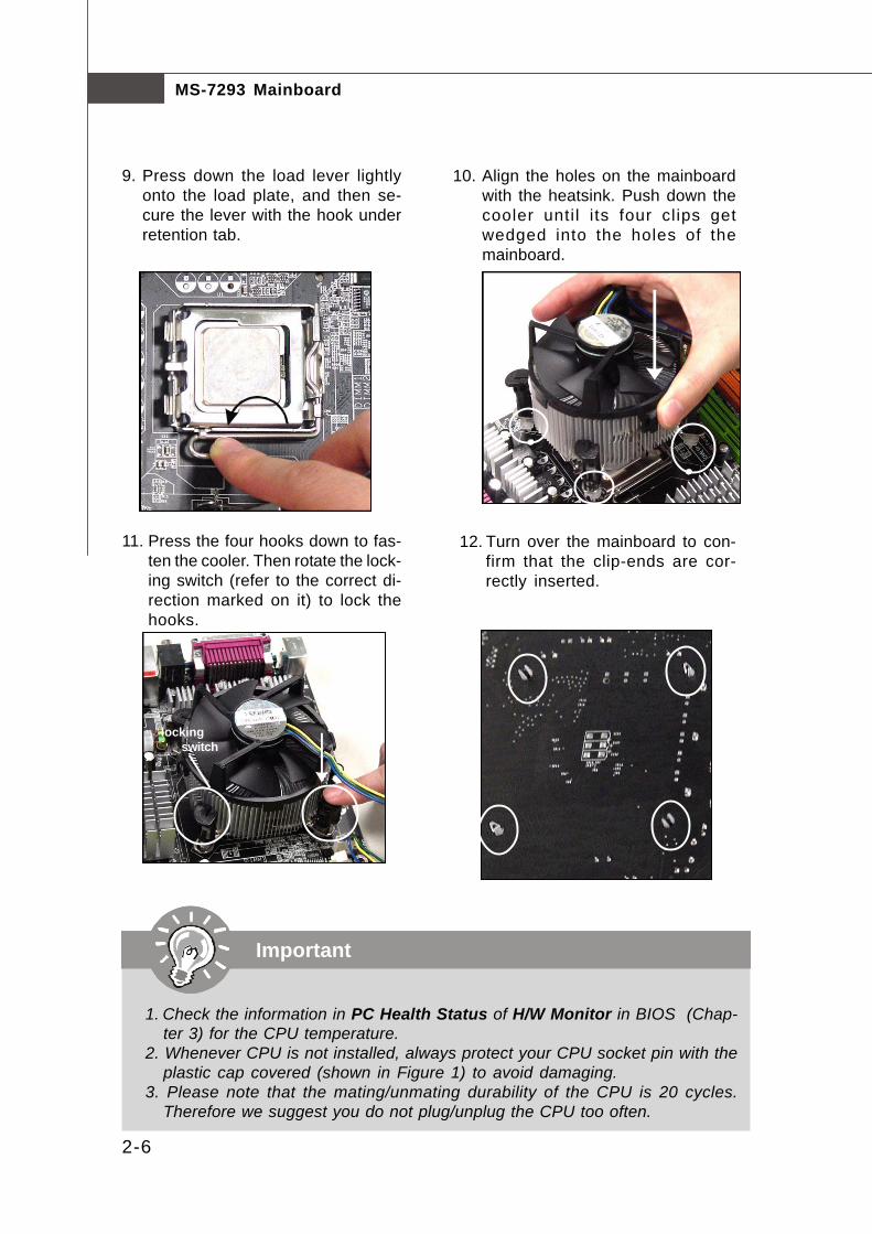
Important
1. Check the information in PC Health Status of H/W Monitor in BIOS (Chap-ter 3) for the CPU temperature.
2. Whenever CPU is not installed, always protect your CPU socket pin with theplastic cap covered (shown in Figure 1) to avoid damaging.
3. Please note that the mating/unmating durability of the CPU is 20 cycles.Therefore we suggest you do not plug/unplug the CPU too often.
10. Align the holes on the mainboardwith the heatsink. Push down thecooler until its four clips getwedged into the holes of themainboard.
12. Turn over the mainboard to con-firm that the clip-ends are cor-rectly inserted.
11. Press the four hooks down to fas-ten the cooler. Then rotate the lock-ing switch (refer to the correct di-rection marked on it) to lock thehooks.
9. Press down the load lever lightlyonto the load plate, and then se-cure the lever with the hook underretention tab.
lockingswitch
2-7
Hardware Setup
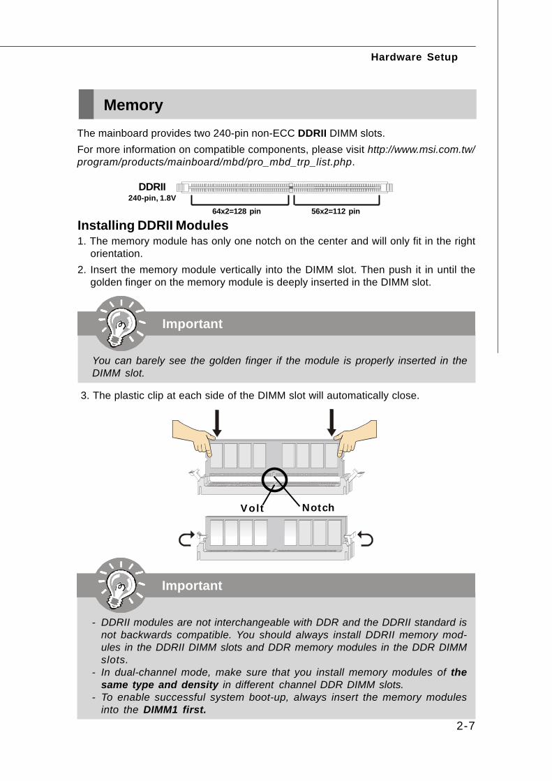
MemoryThe mainboard provides two 240-pin non-ECC DDRII DIMM slots.For more information on compatible components, please visit http://www.msi.com.tw/program/products/mainboard/mbd/pro_mbd_trp_list.php.
64x2=128 pin 56x2=112 pin
DDRII240-pin, 1.8V
Important
- DDRII modules are not interchangeable with DDR and the DDRII standard isnot backwards compatible. You should always install DDRII memory mod-ules in the DDRII DIMM slots and DDR memory modules in the DDR DIMMslots.
- In dual-channel mode, make sure that you install memory modules of thesame type and density in different channel DDR DIMM slots.
- To enable successful system boot-up, always insert the memory modulesinto the DIMM1 first.
Installing DDRII Modules1. The memory module has only one notch on the center and will only fit in the right
orientation.2. Insert the memory module vertically into the DIMM slot. Then push it in until the
golden finger on the memory module is deeply inserted in the DIMM slot.
3. The plastic clip at each side of the DIMM slot will automatically close.
Volt Notch
Important
You can barely see the golden finger if the module is properly inserted in theDIMM slot.

MS-7293 Mainboard
2-8
Power Supply
PIN SIGNAL
13 +3.3V14 -12V15 GND16 PS-ON#17 GND18 GND19 GND20 Res21 +5V22 +5V23 +5V24 GND
PIN SIGNAL
1 +3.3V 2 +3.3V 3 GND 4 +5V 5 GND 6 +5V 7 GND 8 PWR OK 9 5VSB10 +12V11 +12V12 NC
ATX1 Pin Definition
PIN SIGNAL
1 GND2 GND3 12V4 12V
JPW1 Pin Definition
pin 12
pin 13
JPW1
Important
1. Maker sure that all the connectors are connected to proper ATX power sup-plies to ensure stable operation of the mainboard.
2. Power supply of 350 watts (and above) is highly recommended for systemstability.
3. ATX 12V power connection should be greater than 18A.
ATX 24-Pin Power Connector: ATX1This connector allows you to connect an ATX 24-pin power supply.To connect the ATX 24-pin power supply, make sure the plug of thepower supply is inserted in the proper orientation and the pins arealigned. Then push down the power supply firmly into the connec-tor.There is also a foolproof design on pin 23 & 24 to avoid wronginstallation.
ATX 12V Power Connector: JPW1This 12V power connector is used to provide power to the CPU.
2
13
4
1
ATX1
1224
13

2-9
Hardware Setup
Back Panel
Serial Port ConnectorThe serial port is a 16550A high speed communications port that sends/ receives 16bytes FIFOs. You can attach a serial mouse or other serial devices directly to theconnector.
IEEE 1394 PortThe 1394 port on the back panel provides connection to 1394 devices.
USB ConnectorsThe OHCI (Open Host Controller Interface) Universal Serial Bus root is for attachingUSB devices such as keyboard, mouse, or other USB-compatible devices.
LAN (RJ-45) JackThe standard RJ-45 jack is for connection to single Local Area Network (LAN). Youcan connect a network cable to it.
Link IndicatorActivity Indicator
LED Color LED State Condition
Off LAN link is not established.
Left Orange On (steady state) LAN link is established.
On (brighter & pulsing) The computer is communicating with another computer on the LAN.
Green Off 10 Mbit/sec data rate is selected.
Right On 100 Mbit/sec data rate is selected.
Orange On 1000 Mbit/sec data rate is selected.
USB Ports
L-In
1394 Port LAN
Serial Port
RS-Out
SS-OutCS-OutL-Out
MicSPDIF-Out
MS-7293 Mainboard
2-10
Optical SPDIF-Out connectorThis SPDIF (Sony & Philips Digital Interconnect Format) connector is provided fordigital audio transmission to external speakers through an optical cable.
Audio Port ConnectorsThese audio connectors are used for audio devices. You can differentiate the colorof the audio jacks for different audio sound effects.
Blue audio jack - Line In, is used for external CD player, tapeplayeror other audio devices.
Green audio jack - Line Out, is a connector for speakers or headphones. Pink audio jack - Mic In, is a connector for microphones. Black audio jack - Rear-Surround Out in 4.1/ 5.1/ 7.1 channel mode. Orange audio jack - Center/ Subwoofer Out in 5.1/ 7.1 channel mode. Gray audio jack - Side-Surround Out in 7.1 channel mode.

2-11
Hardware Setup
Connectors
Floppy Disk Drive Connector: FDD1This standard FDD connector supports 360K, 720K, 1.2M, 1.44M and 2.88M floppydisk types.
FDD1
IDE1 (Primary IDE Connector)IDE1 can connect a Master and a Slave drive. You mustconfigure the second hard drive to Slave mode by settingthe jumper accordingly.
IDE2 (Secondary IDE Connector)IDE2 can also connect a Master and a Slave drive.
ATA133 Hard Disk Connectors: IDE1 & IDE2The mainboard has a 32-bit Enhanced PCI IDE and Ultra DMA 66/100/133 controllerthat provides PIO mode 0~4, Bus Master, and Ultra DMA 66/100/133 function. You canconnect hard disk drives, CD-ROM and other IDE devices.The Ultra ATA133 interface boosts data transfer rates between the computer and thehard drive up to 133 megabytes (MB) per second. The new interface is one-thirdfaster than earlier record-breaking Ultra ATA/100 technology and is backwardscompatible with the existing Ultra ATA interface.
Important
If you install two hard disks on cable, you must configure the second drive toSlave mode by setting its jumper. Refer to the hard disk documentationsupplied by hard disk vendors for jumper setting instructions.
IDE2IDE1

MS-7293 Mainboard
2-12
PIN SIGNAL PIN SIGNAL
1 GND 2 RXN3 RXP 4 GND5 TXN 6 TXP7 GND
SATA1, SATA2 Pin Definition
Connect to SATA1, 2Take out the dust coverand connect to the harddisk devices
Serial ATA cable
Serial ATA Connectors: SATA1, SATA2SATA1, SATA2 are high-speed Serial ATA interface ports. Each supports 1st genera-tion serial ATA data rates of 150MB/s and is fully compliant with Serial ATA 1.0specifications. Each Serial ATA connector can connect to 1 hard disk device.
7 1
SATA1
SATA2
7 1
Important
Please do not fold the Serial ATA cable into 90-degree angle. Otherwise,data loss may occur during transmission.
BIOS Password Clear: JPWD1The BIOS password protects the BIOS from undesired changes. If youneed to clear the BIOS password, use the following steps: JPWD1
21
1. Turn off the system, then remove the jumper from JPWD1.2. Power on the system, and BIOS would show “Password Cleared By Jumper” during POST.3. Press DEL key to enter BIOS Setup menu, and you’ll find the BIOS passwords are cleared.4. Turn off the system, and put the jumper back on JPWD1.
2-13
Hardware Setup
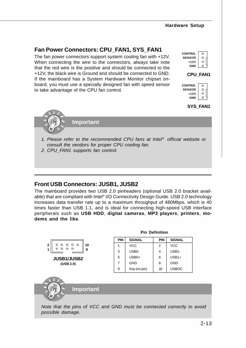
Fan Power Connectors: CPU_FAN1, SYS_FAN1The fan power connectors support system cooling fan with +12V.When connecting the wire to the connectors, always take notethat the red wire is the positive and should be connected to the+12V, the black wire is Ground and should be connected to GND.If the mainboard has a System Hardware Monitor chipset on-board, you must use a specially designed fan with speed sensorto take advantage of the CPU fan control.
Important
1. Please refer to the recommended CPU fans at Intel® official website orconsult the vendors for proper CPU cooling fan.
2. CPU_FAN1 supports fan control.
PIN SIGNAL PIN SIGNAL1 VCC 2 VCC
3 USB0- 4 USB1-5 USB0+ 6 USB1+
7 GND 8 GND
9 Key (no pin) 10 USBOC
Pin Definition
Important
Note that the pins of VCC and GND must be connected correctly to avoidpossible damage.
JUSB1/JUSB2(USB 2.0)
1 2 10
9
Front USB Connectors: JUSB1, JUSB2The mainboard provides two USB 2.0 pinheaders (optional USB 2.0 bracket avail-able) that are compliant with Intel® I/O Connectivity Design Guide. USB 2.0 technologyincreases data transfer rate up to a maximum throughput of 480Mbps, which is 40times faster than USB 1.1, and is ideal for connecting high-speed USB interfaceperipherals such as USB HDD, digital cameras, MP3 players, printers, mo-dems and the like.
SYS_FAN1
SENSOR+12VGND
CONTROL
CPU_FAN1
SENSOR+12VGND
CONTROL
MS-7293 Mainboard
2-14
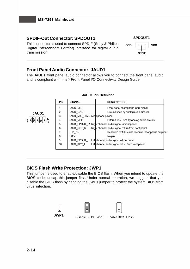
Front Panel Audio Connector: JAUD1The JAUD1 front panel audio connector allows you to connect the front panel audioand is compliant with Intel® Front Panel I/O Connectivity Design Guide.
PIN SIGNAL DESCRIPTION
1 AUD_MIC Front panel microphone input signal2 AUD_GND Ground used by analog audio circuits3 AUD_MIC_BIAS Microphone power4 AUD_VCC Filtered +5V used by analog audio circuits5 AUD_FPOUT_R Right channel audio signal to front panel6 AUD_RET_R Right channel audio signal return from front panel7 HP_ON Reserved for future use to control headphone amplifier8 KEY No pin9 AUD_FPOUT_L Left channel audio signal to front panel10 AUD_RET_L Left channel audio signal return from front panel
JAUD1 Pin Definition
JAUD1
12
910
SPDIF-Out Connector: SPDOUT1This connector is used to connect SPDIF (Sony & PhilipsDigital Interconnect Format) interface for digital audiotransmission.
SPDOUT1
GND
SPDIF
VCC
BIOS Flash Write Protection: JWP1This jumper is used to enable/disable the BIOS flash. When you intend to update theBIOS code, uncap this jumper first. Under normal operation, we suggest that youdisable the BIOS flash by capping the JWP1 jumper to protect the system BIOS fromvirus infection.
JWP1 Enable BIOS FlashDisable BIOS Flash
2-15
Hardware Setup
PIN SIGNAL DESCRIPTION
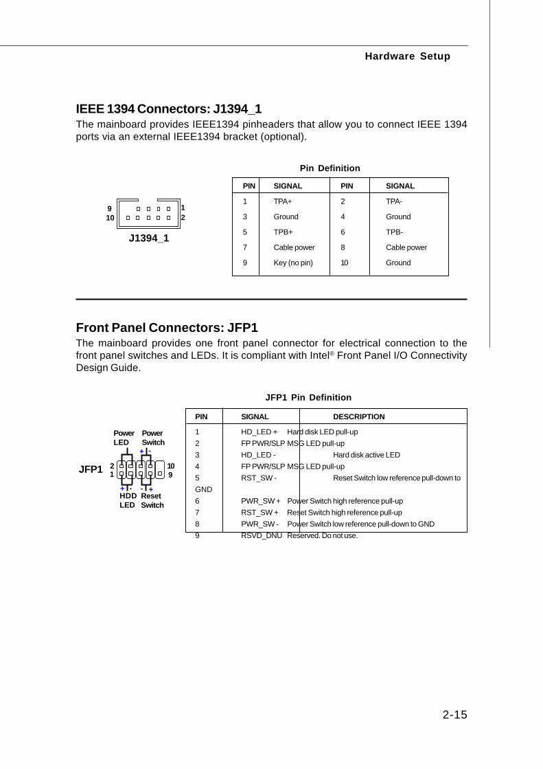
1 HD_LED + Hard disk LED pull-up2 FP PWR/SLP MSG LED pull-up3 HD_LED - Hard disk active LED4 FP PWR/SLP MSG LED pull-up5 RST_SW - Reset Switch low reference pull-down toGND6 PWR_SW + Power Switch high reference pull-up7 RST_SW + Reset Switch high reference pull-up8 PWR_SW - Power Switch low reference pull-down to GND9 RSVD_DNU Reserved. Do not use.
JFP1 Pin Definition
Front Panel Connectors: JFP1The mainboard provides one front panel connector for electrical connection to thefront panel switches and LEDs. It is compliant with Intel® Front Panel I/O ConnectivityDesign Guide.
12
910JFP1
HDDLED
ResetSwitch
PowerLED
PowerSwitch
+ +
+
- -
-
IEEE 1394 Connectors: J1394_1The mainboard provides IEEE1394 pinheaders that allow you to connect IEEE 1394ports via an external IEEE1394 bracket (optional).
Pin Definition
PIN SIGNAL PIN SIGNAL
1 TPA+ 2 TPA-
3 Ground 4 Ground
5 TPB+ 6 TPB-
7 Cable power 8 Cable power
9 Key (no pin) 10 Ground
J1394_1
1 2
9 10

MS-7293 Mainboard
2-16
Jumpers
Clear CMOS Jumper: JBAT1There is a CMOS RAM onboard that has a power supply from external battery to keepthe data of system configuration. With the CMOS RAM, the system can automaticallyboot OS every time it is turned on. If you want to clear the system configuration, setthe JBAT1 (Clear CMOS Jumper ) to clear data.
Important
You can clear CMOS by shorting 2-3 pin while the system is off. Then returnto 1-2 pin position. Avoid clearing the CMOS while the system is on; it willdamage the mainboard.
JBAT11
Clear Data
3
1
Keep Data
3
1
BIOS Recovery: JBR1To recover the BIOS, you have to insert certain boot disk into the floppy drive beforepowering on the system. After powered on, the system will read the boot disk andenter DOS. This enables you to update the BIOS automatically.
JBR1Normal Mode Recovery Mode

2-17
Hardware Setup
PCI (Peripheral Component Interconnect) Express SlotsPCI Express architecture provides a high performance I/O infrastructure for DesktopPlatforms with transfer rates starting at 2.5 Giga transfers per second over a PCIExpress x1 lane for Gigabit Ethernet, TV Tuners, 1394 controllers, and general pur-pose I/O. Also, desktop platforms with PCI Express Architecture will be designed todeliver highest performance in video, graphics, multimedia and other sophisticatedapplications. Moreover, PCI Express architecture provides a high performance graph-ics infrastructure for Desktop Platforms doubling the capability of existing AGP 8xdesigns with transfer rates of 4.0 GB/s over a PCI Express x16 lane for graphicscontrollers, while PCI Express x1 supports transfer rate of 250 MB/s.
PCI (Peripheral Component Interconnect) SlotsThe PCI slots support LAN cards, SCSI cards, USB cards, and other add-on cardsthat comply with PCI specifications. At 32 bits and 33 MHz, it yields a throughput rateof 133 MBps.
Slots
PCI Express x16 Slot
PCI Express x1 Slot
Important
When adding or removing expansion cards, make sure that you unplug thepower supply first. Meanwhile, read the documentation for the expansion cardto configure any necessary hardware or software settings for the expansioncard, such as jumpers, switches or BIOS configuration.
32-bit PCI Slot
MS-7293 Mainboard
2-18
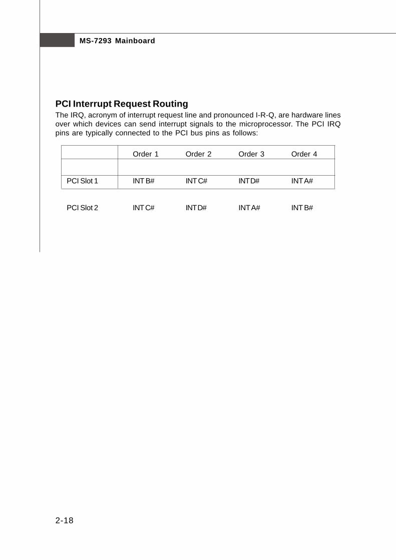
PCI Interrupt Request RoutingThe IRQ, acronym of interrupt request line and pronounced I-R-Q, are hardware linesover which devices can send interrupt signals to the microprocessor. The PCI IRQpins are typically connected to the PCI bus pins as follows:
Order 1 Order 2 Order 3 Order 4
PCI Slot 1 INT B# INT C# INT D# INT A#
PCI Slot 2 INT C# INT D# INT A# INT B#
3-1
BIOS Setup
Chapter 3
BIOS Setup
This chapter provides information on the BIOS Setupprogram and allows you to configure the system foroptimum use.You may need to run the Setup program when:
An error message appears on the screen during thesystem booting up, and requests you to run SETUP.You want to change the default settings for cus-tomized features.
3-2
MS-7293 Mainboard
Entering Setup
Important
1. The items under each BIOS category described in this chapter are undercontinuous update for better system performance. Therefore, the descrip-tion may be slightly different from the latest BIOS and should be held forreference only.
2. Upon boot-up, the 1st line appearing after the memory count is the BIOSversion. It is usually in the format:
W7293VMS V2.0 102006 where:
1st digit refers to BIOS maker as A = AMI, W = AWARD, and P =PHOENIX.2nd - 5th digit refers to the model number.6th digit refers to the chipset as I = Intel, N = nVidia, and V = VIA.7th - 8th digit refers to the customer as MS = all standard customers.V2.0 refers to the BIOS version.102006 refers to the date this BIOS was released.
Power on the computer and the system will start POST (Power On Self Test) process.When the message below appears on the screen, press <DEL> key to enter Setup.
Press DEL to enter SETUP
If the message disappears before you respond and you still wish to enter Setup,restart the system by turning it OFF and On or pressing the RESET button. You mayalso restart the system by simultaneously pressing <Ctrl>, <Alt>, and <Delete> keys.

3-3
BIOS Setup
Getting HelpAfter entering the Setup menu, the first menu you will see is the Main Menu.
Main MenuThe main menu lists the setup functions you can make changes to. You can use thearrow keys ( ↑↓ ) to select the item. The on-line description of the highlighted setupfunction is displayed at the bottom of the screen.
Sub-MenuIf you find a right pointer symbol (as shown in the rightview) appears to the left of certain fields that means asub-menu can be launched from this field. A sub-menucontains additional options for a field parameter. Youcan use arrow keys ( ↑↓ ) to highlight the field andpress <Enter> to call up the sub-menu. Then you can use the control keys to entervalues and move from field to field within a sub-menu. If you want to return to themain menu, just press the <Esc >.
General Help <F1>The BIOS setup program provides a General Help screen. You can call up this screenfrom any menu by simply pressing <F1>. The Help screen lists the appropriate keysto use and the possible selections for the highlighted item. Press <Esc> to exit theHelp screen.
Control Keys
<↑> Move to the previous item<↓> Move to the next item<←> Move to the item in the left hand<→> Move to the item in the right hand<Enter> Select the item<Esc> Jumps to the Exit menu or returns to the main menu from a
submenu<+/PU> Increase the numeric value or make changes<-/PD> Decrease the numeric value or make changes<F1> General Help<F6> Load Optimized Defaults<F10> Save all the CMOS changes and exit
3-4
MS-7293 Mainboard
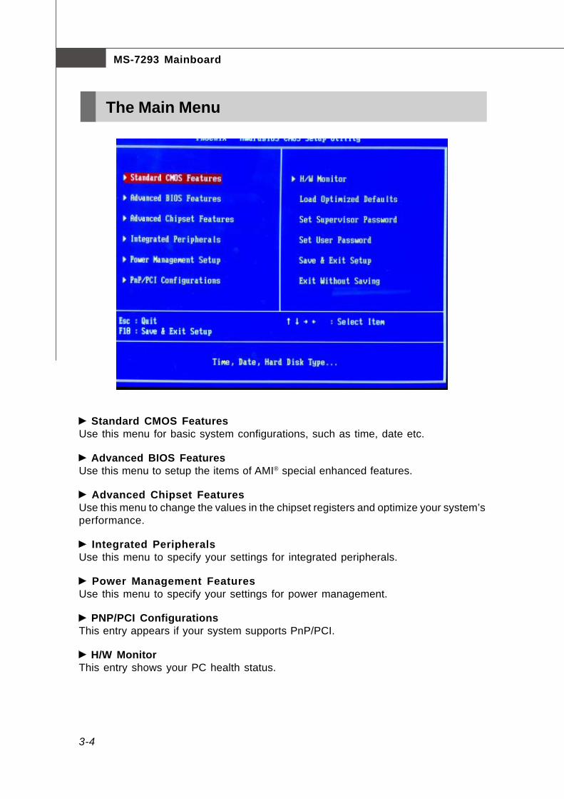
Standard CMOS FeaturesUse this menu for basic system configurations, such as time, date etc.
Advanced BIOS FeaturesUse this menu to setup the items of AMI® special enhanced features.
Advanced Chipset FeaturesUse this menu to change the values in the chipset registers and optimize your system’sperformance.
Integrated PeripheralsUse this menu to specify your settings for integrated peripherals.
Power Management FeaturesUse this menu to specify your settings for power management.
PNP/PCI ConfigurationsThis entry appears if your system supports PnP/PCI.
H/W MonitorThis entry shows your PC health status.
The Main Menu
3-5
BIOS Setup
Load Optimized DefaultsUse this menu to load the default values set by the mainboard manufacturer specifi-cally for optimal performance of the mainboard.
Set Supervisor PasswordUse this menu to set the supervisor password for BIOS.
Set User PasswordUse this menu to set the user password for BIOS.
Save & Exit SetupSave changes to CMOS and exit setup.
Exit Without SavingAbandon all changes and exit setup.

3-6
MS-7293 Mainboard
The items in Standard CMOS Features Menu includes some basic setup items. Usethe arrow keys to highlight the item and then use the <PgUp> or <PgDn> keys to selectthe value you want in each item.
Date (mm:dd:yy)This allows you to set the system to the date that you want (usually the current date).The format is <day><month> <date> <year>.
day Day of the week, from Sun to Sat, determined byBIOS. Read-only.
month The month from Jan. through Dec.date The date from 1 to 31 can be keyed by numeric function keys.year The year can be adjusted by users.
Time (hh:mm:ss)This allows you to set the system time that you want (usually the current time). Thetime format is <hour> <minute> <second>.
IDE Channel 0/1/2/3 Master/ SlavePress <Enter> to enter the sub-menu.
Access ModeSelect Access Mode.
DMA ModeSelect DMA Mode.
Standard CMOS Features
3-7
BIOS Setup
Important
IDE Channel 0/1/2/3 Master/ Slave are appearing when you connect theHD devices to the SATA connector on the mainboard.
Drive AThis item allows you to set the type of floppy drives installed.
Halt OnThe setting determines whether the system will stop if an error is detected at boot.Available options are:
[No Errors] The system doesn’t stop for any detected error.[All, But Keyboard] The system doesn’t stop for a keyboard error.
System InformationPress <Enter> to enter the sub-menu.This sub-menu shows the CPU information, BIOS version and memory status of yoursystem (read only).
3-8
MS-7293 Mainboard
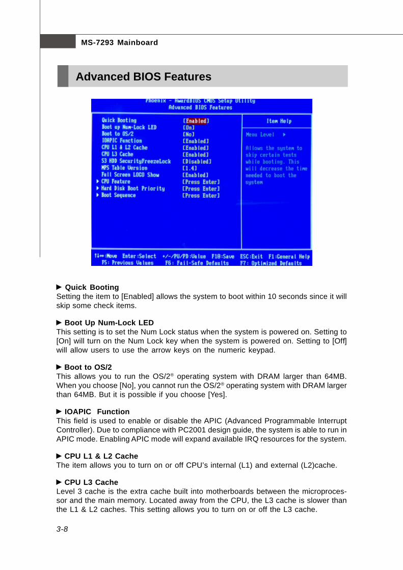
Quick BootingSetting the item to [Enabled] allows the system to boot within 10 seconds since it willskip some check items.
Boot Up Num-Lock LEDThis setting is to set the Num Lock status when the system is powered on. Setting to[On] will turn on the Num Lock key when the system is powered on. Setting to [Off]will allow users to use the arrow keys on the numeric keypad.
Boot to OS/2This allows you to run the OS/2® operating system with DRAM larger than 64MB.When you choose [No], you cannot run the OS/2® operating system with DRAM largerthan 64MB. But it is possible if you choose [Yes].
IOAPIC FunctionThis field is used to enable or disable the APIC (Advanced Programmable InterruptController). Due to compliance with PC2001 design guide, the system is able to run inAPIC mode. Enabling APIC mode will expand available IRQ resources for the system.
CPU L1 & L2 CacheThe item allows you to turn on or off CPU’s internal (L1) and external (L2)cache.
CPU L3 CacheLevel 3 cache is the extra cache built into motherboards between the microproces-sor and the main memory. Located away from the CPU, the L3 cache is slower thanthe L1 & L2 caches. This setting allows you to turn on or off the L3 cache.
Advanced BIOS Features
3-9
BIOS Setup
S3 HDD Security FreezeLockThis field allows you to enable or disable the HDD security in S3.
MPS Table VersionThis field allows you to select which MPS (Multi-Processor Specification) version tobe used for the operating system. You need to select the MPS version supported byyour operating system. To find out which version to use, consult the vendor of youroperating system.
Full Screen LOGO DisplayThis item enables you to show the company logo on the bootup screen. Settings are:
[Enabled] Shows a still image (logo) on the full screen at boot.[Disabled] Shows the POST messages at boot.
CPU FeaturePress <Enter> to enter the sub-menu:
Limit CPUID MaxValThe item allows you to enable/ disable the CPU ID maximum value.[Enabled] Set to [Enabled] only when you have Prescott CPU and NT4.0
operating system.[Disabled] Set to [Disabled] if you have operating system other than NT4.0.
C1E FunctionWhen the C1E Support (Enhanced Halt Powerdown State) is enabled, the proc-essor will transition to a lower core to bus ratio and lower voltage ID driven bythe processor to the voltage regulator before entering Halt Powerdown State(C1). Not all porcessors support Enhanced Halt Powerdown State (C1E). Youcan enable C1E Support to lower the CPU power consumption while idle.
Execute Disable BitExcute Bit Support function is designed for memory buffer overflow protection,it can prevent viruses from proliferating.
Virtualization TechnologyIt allows you to enable or disable the Virtualzation Technology.
Hard Disk Boot PriorityPress <Enter> to enter the sub-menu and set the sequency of boot hard disk.
Boot SequencePress <Enter> to enter the sub-menu:
1st/2nd/3rd Boot DeviceThe items allow you to set the sequence of boot devices where BIOS attemptsto load the disk operating system.

3-10
MS-7293 Mainboard
Advanced Chipset Features
DRAM Clock/ Drive ControlPress <Enter> to enter the sub-menu:
Current FSB/ DRAM FrequencyThese items show the current FSB/ DRAM frequency (Read only).
DRAM ClockIt allows you to select the DRAM clock.
DRAM TimingThis field allows you to select the DDR timing setting. Setting to Auto By SPDenables DRAM timing automatically to be determined by SPD. Selecting Manualallows users to configure these fields manually.
SDRAM CAS Latency [DDR/DDR2]When the DRAM Timing sets to [Manual], the field is adjustable.This controlsthe CAS latency, which determines the timing delay (in clock cycles) beforeSDRAM starts a read command after receiving it.
Bank InterleaveWhen the DRAM Timing sets to [Manual], the field is adjustable. This fieldselects 2-bank or 4-bank interleave for the installed SDRAM. Disable the func-tion if 16MB SDRAM is installed.

3-11
BIOS Setup
Precharge to Active (Trp)When the DRAM Timing sets to [Manual], the field is adjustable. This itemcontrols the number of cycles for Row Address Strobe (RAS) to be allowed toprecharge. If insufficient time is allowed for the RAS to accumulate its chargebefore DRAM refresh, refreshing may be incomplete and DRAM may fail toretain data. This item applies only when synchronous DRAM is installed in thesystem.
Active to Precharge (Tras)When the DRAM Timing sets to [Manual], the field is adjustable. This settingdetermines the time RAS takes to read from and write to a memory cell.
Active to CMD (Trcd)When the DRAM Timing sets to [Manual], the field is adjustable. When DRAMis refreshed, both rows and columns are addressed separately. This setup itemallows you to determine the timing of the transition from RAS (row addressstrobe) to CAS (column address strobe). The less the clock cycles, the fasterthe DRAM performance.
REF to ACT/REF (Trfc)When the DRAM Timing sets to [Manual], the field is adjustable. Auto-refresh-active to RAS#-active or RAS# auto-refresh.
ACT(0) to ACT(1) (TRRD)When the DRAM Timing sets to [Manual], the field is adjustable.Specifies theactive-to-active delay of different banks. When DRAM is refreshed, both rowsand columns are addressed separately. This setup item allows you to determinethe timing of the transition from RAS (row address strobe) to CAS (columnaddress strobe). The less the clock cycles, the faster the DRAM performance.
1T CMD SupportIt allows to enable or disable the 1T command rate.
CPU & PCI Bus ControlPress <Enter> to enter the sub-menu:
PCI Master 0 WS WriteWhen [Enabled], writes to the PCI bus are executed with zero wait states.
PCI Delayed TransactionThe chipset has an embedded 32-bit posted write buffer to support delay trans-actions cycles. Select [Enabled] to support compliance with PCI specification.
VLink mode selectionThis item lets you choose the speed mode between the North Bridge & SouthBridge.
3-12
MS-7293 Mainboard
VLink 8X SupportedThis item enables or disables the 8X VLink Data Rate.
VIA PWR ManagementThis item enables or disables the VIA power management function.
Memory HoleIn order to improve performance, certain space in memory can be reserved for ISAperipherals. This memory must be mapped into the memory space below 16MB. Whenthis area is reserved, it cannot be cached.
System BIOS CacheableSelecting [Enabled] allows caching of the system BIOS ROM at F0000h-FFFFFh,resulting in better system performance. However, if any program writes to this memoryarea, a system error may result.
Top PerformanceSet this item to Enabled to increase the system performance.

3-13
BIOS Setup
Integrated Peripherals
VIA OnChip IDE DevicePress <Enter> to enter the sub-menu:
SATA ControllerIt allows you to enable/ disable the SATA controller.
SATA Controller ModeIt lets you select the SATA controller mode.
IDE DMA transfer accessSetting to [Enabled] will open DMA bus master and execute DMA action in DOS,which will make the data transferring faster.
OnChip IDE Channel 0/1These allow you to enable/disable the IDE channel 0/1.
IDE Prefetch ModeThe onboard IDE drive interfaces support IDE prefetching, for faster driveaccesses. When you install a primary and/or secondary add-in IDE interface,set this option to Disabled if the interface does not support prefetching.
VIA OnChip PCI DevicePress <Enter> to enter the sub-menu:
Azalia HDA ControllerIt allows you to enable/ disable the Azalia HDA controller.

3-14
MS-7293 Mainboard
LAN ControllerIt allows you to enable/ disable the LAN controller.
Lan Boot ROMThis item is used to decide whether to invoke the Boot ROM of the Onboard LANChip.
Onboard IEEE1394 ControllerThis item allows you to enable/disable the onboard IEEE1394 controller.
Super IO DevicePress <Enter> to enter the sub-menu:
Onboard FDC ControllerSelect [Enabled] if your system has a floppy disk controller (FDD) installed on thesystem board and you wish to use it. If you install add-on FDC or the system hasno floppy drive, select [Disabled] in this field.
Onboard Serial Port 1Select an address and corresponding interrupt for the first serial port.
USB Device SettingPress <Enter> to enter the sub-menu:
USB 1.0/ 2.0 ControllerThese items allow you to enable/ disable USB 1.0/ 2.0 controller.
USB Operation ModeIt lets you select the operation mode for USB.
USB Keyboard FunctionSelect Enabled if you use the USB keyboard.
USB Mouse FunctionSelect Enabled if you use the USB Mouse.
USB Storage FunctionSelect Enabled if you use the USB Storage device.

3-15
BIOS Setup
ACPI FunctionThis item is to activate the ACPI (Advanced Configuration and Power ManagementInterface) Function. If your operating system is ACPI-aware, such as Windows 2000/XP, select [Yes].
ACPI Standby StateThis item specifies the power saving modes for ACPI function. If your operatingsystem supports ACPI, such as Windows 2000/ XP , you can choose to enter theStandby mode in S1(POS) or S3(STR) fashion through the setting of this field. Set-tings are:
[S1/POS] The S1 sleep mode is a low power state. In this state, nosystem context is lost (CPU or chipset) and hardware main-tains all system context.
[S3/STR] The S3 sleep mode is a lower power state where the information of system configuration and open applications/filesis saved to main memory that remains powered while mostother hardware components turn off to save energy. Theinformation stored in memory will be used to restore the sys-tem when a “wake up” event occurs.
[Auto]
Power Management Setup
Important
S3-related functions described in this section are available only when yourBIOS supports S3 sleep mode.

3-16
MS-7293 Mainboard
Re-Call VGA BIOS From S3When ACPI Standby State is set to [S3/STR], users can select the options in thisfield. Selecting [Yes] allows BIOS to call VGABIOS to initialize the VGA card whensystem wakes up (resumes) from S3 sleep state. The system resume time is short-ened when you disable the function, but system will need an VGA driver to initializethe VGA card. Therefore, if the VGA driver of the card does not support the initializa-tion feature, the display may work abnormally or not function after resuming from S3.
Suspend Time Out (Minute)If system activity is not detected for the length of time specified in this field, alldevices except CPU will be shut off.
Power Button FunctionThis feature sets the function of the power button. Settings are:
[On/ Off] The power button functions as normal power off button.[Suspend] When you press the power button, the computer enters the
suspend/sleep mode, but if the button is pressed for morethan four seconds, the computer is turned off.
Restore On AC Power LossThis item specifies whether your system will reboot after a power failure or interruptoccurs. Settings are:
[Power Off] Always leaves the computer in the power off state.[Power On] Always leaves the computer in the power on state.[Last State] Restores the system to the status before power failure
or interrupt occurred.
Wakeup Event SetupPress <Enter> to enter the sub-menu:
Resume From S3 By USB DeviceThe item allows the activity of the USB device to wake up the system from S3(Suspend to RAM) sleep state.
Resume By PCI-E DeviceWhen set to [Enabled], the feature allows your system to be awakened from thepower saving modes through any event on PCIE device.
Resume by PCI CardWhen set to [Enabled], the feature allows your system to be awakened from thepower saving modes through any event on PCI device.
RTC Alarm ResumeThe field is used to enable or disable the feature of booting up the system on ascheduled time/date.

3-17
BIOS Setup
Date (of Month) AlarmThe field specifies the date for Resume by RTC Alarm.
Time (hh:mm:ss) AlarmThe field specifies the time for Resume by RTC Alarm . Format is<hour><minute><second>.

3-18
MS-7293 Mainboard
Primary Graphics AdapterThis setting specifies which graphics card is your primary graphics adapter.
PCI Latency Timer (CLK)This item controls how long each PCI device can hold the bus before another takesover. When set to higher values, every PCI device can conduct transactions for alonger time and thus improve the effective PCI bandwidth. For better PCI performance,you should set the item to higher values.
** PCI Express relative items ** Maximum Payload Size
This item allows you to set the PCI Express Maximum payload size per time .
PNP/PCI ConfigurationsThis section describes configuring the PCI bus system and PnP (Plug & Play) feature.PCI, or Peripheral Component Interconnect, is a system which allows I/O devices tooperate at speeds nearing the speed the CPU itself uses when communicating withits special components. This section covers some very technical items and it isstrongly recommended that only experienced users should make any changes to thedefault settings.

3-19
BIOS Setup
CPU Shutdown TemperatureIf the CPU temperature reaches the upper limit preset in this setting, the system will beshut down automatically. This helps you to prevent the CPU overheating problem.This item is available only when your OS supports this function.
CPU Smart Fan Temp.Select a temperature setting here, and if the temperature of the CPU climbs up to theselected temperature setting, the system will automatically increase the speed of theCPU fan to cool down the overheated CPU.
CPU Temp. ToleranceWhen a particular temperature setting is selected for the previous item, CPU SmartFan Temperature, a temperature tolerance value between 1 to 5 can be adjustedhere.
PC Health StatusPress <Enter> to enter the sub-menu:
System/ CPU Temperature, System/CPU FAN Speed, CPU Vcore, 12V,5VThese items display the current status of all of the monitored hardware devices/components such as CPU voltage, temperatures and all fans’ speeds.
H/W Monitor
3-20
MS-7293 Mainboard
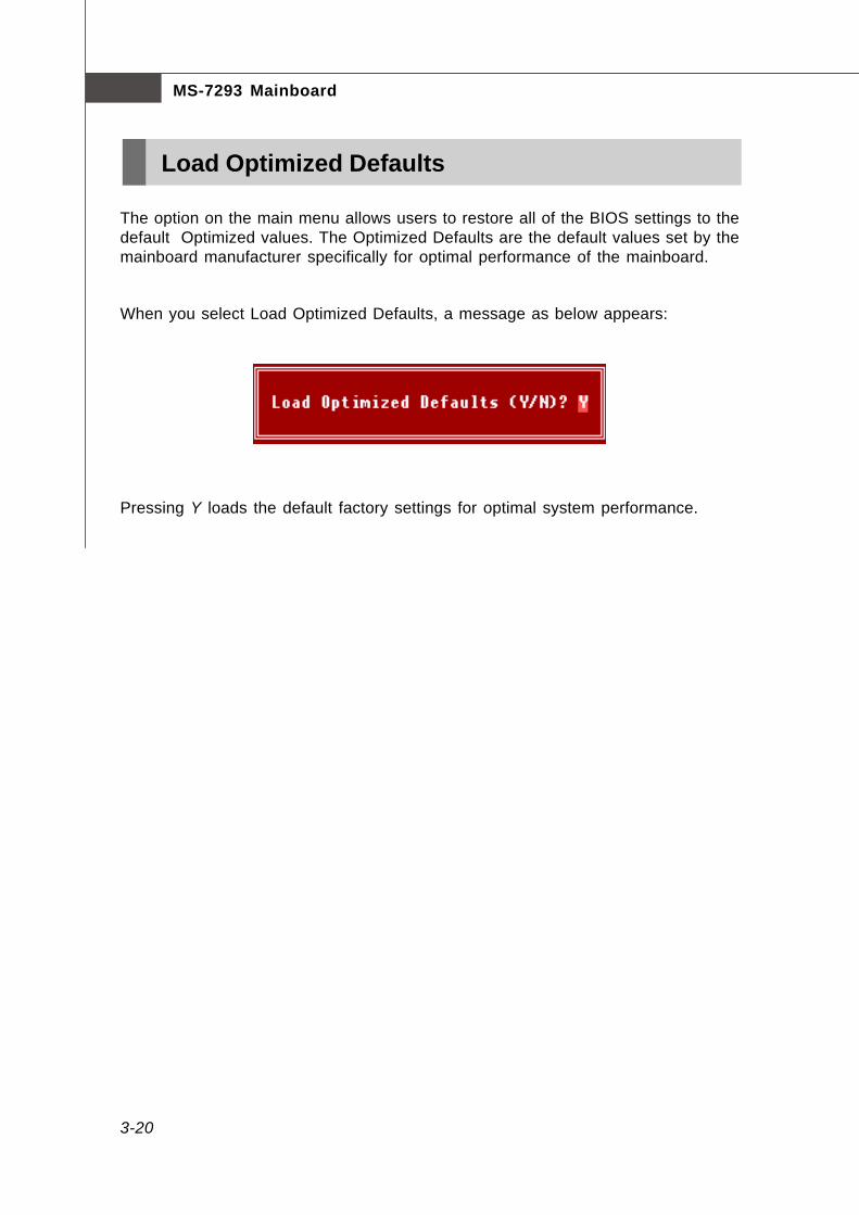
The option on the main menu allows users to restore all of the BIOS settings to thedefault Optimized values. The Optimized Defaults are the default values set by themainboard manufacturer specifically for optimal performance of the mainboard.
When you select Load Optimized Defaults, a message as below appears:
Pressing Y loads the default factory settings for optimal system performance.
Load Optimized Defaults
3-21
BIOS Setup
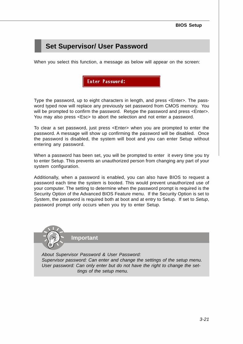
Set Supervisor/ User Password
When you select this function, a message as below will appear on the screen:
Type the password, up to eight characters in length, and press <Enter>. The pass-word typed now will replace any previously set password from CMOS memory. Youwill be prompted to confirm the password. Retype the password and press <Enter>.You may also press <Esc> to abort the selection and not enter a password.
To clear a set password, just press <Enter> when you are prompted to enter thepassword. A message will show up confirming the password will be disabled. Oncethe password is disabled, the system will boot and you can enter Setup withoutentering any password.
When a password has been set, you will be prompted to enter it every time you tryto enter Setup. This prevents an unauthorized person from changing any part of yoursystem configuration.
Additionally, when a password is enabled, you can also have BIOS to request apassword each time the system is booted. This would prevent unauthorized use ofyour computer. The setting to determine when the password prompt is required is theSecurity Option of the Advanced BIOS Feature menu. If the Security Option is set toSystem, the password is required both at boot and at entry to Setup. If set to Setup,password prompt only occurs when you try to enter Setup.
Important
About Supervisor Password & User Password:Supervisor password: Can enter and change the settings of the setup menu.User password: Can only enter but do not have the right to change the set-
tings of the setup menu.