Embed Size (px)
Citation preview
Jana et al. Nanoscale Research Letters (2015) 10:188 DOI 10.1186/s11671-015-0880-9
NANO REVIEW Open Access
Conductive-bridging random access memory:challenges and opportunity for 3D architectureDebanjan Jana1, Sourav Roy1, Rajeswar Panja1, Mrinmoy Dutta1, Sheikh Ziaur Rahaman1, Rajat Mahapatra1,2
and Siddheswar Maikap1*
Abstract
The performances of conductive-bridging random access memory (CBRAM) have been reviewed for different switchingmaterials such as chalcogenides, oxides, and bilayers in different structures. The structure consists of an inert electrodeand one oxidized electrode of copper (Cu) or silver (Ag). The switching mechanism is the formation/dissolution of ametallic filament in the switching materials under external bias. However, the growth dynamics of the metallic filament indifferent switching materials are still debated. All CBRAM devices are switching under an operation current of 0.1 μA to1 mA, and an operation voltage of ±2 V is also needed. The device can reach a low current of 5 pA; however, currentcompliance-dependent reliability is a challenging issue. Although a chalcogenide-based material has opportunity to havebetter endurance as compared to an oxide-based material, data retention and integration with the complementarymetal-oxide-semiconductor (CMOS) process are also issues. Devices with bilayer switching materials show betterresistive switching characteristics as compared to those with a single switching layer, especially a program/eraseendurance of >105 cycles with a high speed of few nanoseconds. Multi-level cell operation is possible, but the stabilityof the high resistance state is also an important reliability concern. These devices show a good data retention of >105 sat >85°C. However, more study is needed to achieve a 10-year guarantee of data retention for non-volatile memoryapplication. The crossbar memory is benefited for high density with low power operation. Some CBRAM devices as achip have been reported for proto-typical production. This review shows that operation current should be optimizedfor few microamperes with a maintaining speed of few nanoseconds, which will have challenges and also opportunitiesfor three-dimensional (3D) architecture.
Keywords: CBRAM; Conductive bridge; Resistive switching; Chalcogenide; Solid electrolyte; Bilayer; Three-dimensional(3D); Memory
ReviewBackgroundIn recent days, resistive random access memory (RRAM)technology is one of the most promising and reliable al-ternative solutions to overcome the scaling bottleneck ofFLASH [1]. The advantages of RRAM devices are theirsimple metal-insulator-metal structure, low fabricationcost, long endurance, and non-volatile properties withlow power consumption, multi-level cell (MLC) oper-ation, and especially excellent scaling below the <11 nmtechnology node [2-5]. One of the RRAM devices isconductive-bridging random access memory (CBRAM),
* Correspondence: [email protected] Film Nano Tech. Lab., Department of Electronic Engineering, ChangGung University, 259 Wen-Hwa 1st Rd., Kwei-Shan, Tao-Yuan 333, TaiwanFull list of author information is available at the end of the article
© 2015 Jana et al.; licensee Springer. This is anAttribution License (http://creativecommons.orin any medium, provided the original work is p
which has high possibility to fulfill the requirements fornext-generation non-volatile memory (NVM) technologyas mentioned in the International Technology Roadmapfor Semiconductors (ITRS) [1]. In addition, major bene-fits are high speed (few nanoseconds) and low voltageoperation (±3 V). Basically, the structure of CBRAM de-vices consists of one metal electrode which is electro-chemically active (i.e., anode) or oxidized under externalpositive bias, such as Ag or Cu, and another one which iselectrochemically inert (i.e., cathode), such as platinum (Pt),iridium (Ir), gold (Au), tungsten (W), or titanium-nitride(TiN). These two electrodes are separated by a solid elec-trolyte or oxide materials. In 1976, Hirose et al. [6] reportedmemory switching using a Ag dendrite in a Ag-dopedAs2S3 film in a Ag/As2S3/Mo structure. In 1999, Kozickiet al. [7] reported a programmable metallization cell (PMC)
Open Access article distributed under the terms of the Creative Commonsg/licenses/by/4.0), which permits unrestricted use, distribution, and reproductionroperly credited.
Jana et al. Nanoscale Research Letters (2015) 10:188 Page 2 of 23
device using metal-doped chalcogenide films. PMC deviceshave different names like electrochemical metallization cell(ECM), ‘atom switch’ [8], or CBRAM [9]. Generally, theyare called ‘CBRAM’. According to their concepts, when apositive voltage is applied on the anode, an electrochemicalreaction occurs, which oxidizes the metal to form ions(Cuz+, z = 1, 2, or Ag+). The cations drift through the solidelectrolyte switching layer under the electric field, and themetal ions are reduced on the inert electrodes. As thisprocess continues, a metallic filament is established in be-tween the two electrodes and the device switches from thehigh resistance state (HRS) to the low resistance state(LRS). By changing the polarity of the voltage, an electro-chemical dissolution of the conductive bridges takes place,resetting the device from the LRS to the HRS. The resist-ance state changes by applying external bias, and theswitching is reversible. It is true that device reliability in-cluding stable switching characteristics, program/erase en-durance, and data retention at 85°C for 10 years at a lowcurrent of few microamperes is a very challenging issuefor production. In addition, the switching mechanism indifferent structures including materials and electrodes isnot understood clearly. Especially, the growth kinetics ofthe metallic filament in oxide- and non-oxide-based mate-rials are still debated. Although the memory performancesof a designed structure with low operation current havehuge opportunities to fulfill the requirements of ITRS,they are not achieved yet. Even though many papers havebeen reported by several groups, a complete review onCBRAM performances including switching characteristics,reliability, mechanism, and so on for real production isneeded, which is not reported yet.Here, the challenges and opportunities of CBRAM de-
vices using different switching materials such as chalco-genides, oxides, and bilayers in different structures havebeen reviewed. Memory performances such as switchingcharacteristics, endurance, multi-level cell operation,and data retention have been discussed. Memory devicescan be operated with an operation current of 0.1 μA to1 mA under an operation voltage of ±2 V. Filamentgrowth dynamics in different switching materials havebeen discussed. Device reliabilities such as switchinguniformity, endurance, and data retention under a fewmicroamperes are very challenging issues. The devicecan be scaled down below the 11 nm technology nodeand has a very good opportunity for non-volatile cross-bar memory for 3D architecture in the near future. Fi-nally, CBRAM as a chip has been discussed for futureproduction.
Materials and deposition methodsCBRAM performance depends on switching materials in-cluding different non-oxides and oxides. The non-oxides,i.e., chalcogenides, are GeSex [10-12], GeS2 [13,14], GeTe
[15], Cu2S [16], Ag2S [8], and so on. The oxide-based ma-terials are Ta2O5 [16,17], SiO2 [18], ZrO2 [19], GeOx
[20,21], and so on. Other materials such as amorphous Si[22] and Si3N4 [23] have been reported also. Some re-ported results show CBRAM characteristics using bilayerswitching materials: one layer is used as a buffer or inter-facial layer and the other one is used as a switching layer.Bilayers such as Cu-Te/GdOx [24], Cu-Te/SiOx [25],MoOx/GdOx [26], TiOx/TaSiOy [27], GeSex/TaOx [28], Ti/TaOx [29], Cu-Te/Al2O3 [30], TiW/Al2O3 [31], and CuTe-C/Al2O3 [32] have been reported by many groups. Depos-ition process parameters of different switching materialsare discussed below.Memory devices using chalcogenide-based switching
materials are reported below. Chalcogenide glasses arebased on the chalcogen elements, and they have a widerange of properties such as optical and electrical ones, asreported in the literature. Several types of chalcogenide-based solid electrolytes have been reported for future re-sistive switching memory applications. Kozicki et al. [10]reported a Ag/Ag33Ge20Se47/Ni PMC device. A 100-nm-thick Ni as a bottom electrode (BE) was fabricated onSiO2/Si substrates. Then, 50-nm-thick Ge70Se30 wasevaporated with the help of a Knudsen-type cell under10−6 Torr vacuum. This approach will help in maintain-ing almost the same level of elementary content of theswitching material. A very low deposition rate of 0.03nm/s was maintained to enhance the step coverage andfilled into the narrow via-holes. Immediately after that, a30-nm-thick Ag film was deposited to form a Ag:GeSesolid electrolyte. In this case, Ag diffusion by exposureto 405-nm ultraviolet (UV) radiation was time consum-ing and cost effective. To avoid this issue, Schindleret al. [11] reported a Ag/Ag-GeSe/Pt structure. Theirmemory cells consisted of a 100-nm-thick continuous PtBE on SiO2/Si substrates. A Si3N4 layer was depositedon Pt by plasma-enhanced chemical vapor deposition(PECVD) method with a deposition rate of 0.2 nm/s.Via-holes with varying diameters from 2.5 to 50 μmwere patterned by optical lithography. The solid electro-lyte layer was 50-nm-thick Ge0.3Se0.7 and was depositedby radio-frequency sputtering or physical vapor depos-ition (PVD) at a rate of 0.2 nm/s. The applied powerranged from 5 to 25 W. The top electrodes were pat-terned by optical lithography. Then, the Ag layer was de-posited by thermal evaporation at a deposition rate of0.5 nm/s. After that, a lift-off process was carried out toobtain the final device. Due to the low melting point ofSe (221°C), it is difficult to control the composition ofGeSe after deposition by sputtering. To keep the samecomposition, the GeSe material was deposited by usingan electron beam evaporator, which we have also re-ported previously [12]. The resistive switching materialand electrodes were deposited by PVD processes such as
Jana et al. Nanoscale Research Letters (2015) 10:188 Page 3 of 23
sputtering, electron beam evaporation, and thermalevaporation. Initially, 8-in. p-type Si (100) wafers wereused to deposit a SiO2 layer with a thickness of approxi-mately 200 nm. The SiO2 layer was grown by thermaloxidation. Then, W or TiN metal was used as a BE onthe SiO2/Si substrates. The thickness of the BE was ap-proximately 200 nm. To design the memory devices, aSiO2 layer with a thickness of approximately 150 nmwas deposited. Lithography was used to pattern via-holes with different nominal areas from 200 × 200 nm2
to 8 × 8 μm2 of the active switching region. After defin-ing the via-hole regions, reactive-ion etching (RIE)process was used to etch the uncovered SiO2 films andto open the W BE contact. Following this, a GexSe1 − x
solid electrolyte with a thickness of approximately 40nm was deposited using an electron beam evaporator.Pure GexSe1 − x (x = 0.2 to 0.5) granules (commerciallyavailable) with different compositions such as Ge0.2Se0.8,Ge0.3Se0.7, Ge0.4Se0.6, and Ge0.5Se0.5 were used for depos-ition. The chamber pressure was 5 × 10⁻⁶ Torr prior todeposition. The deposition rate was 1 to 2 Å/s. Then, aCu top electrode (TE) with a thickness of approximately40 nm was deposited using a thermal evaporator. A 160-nm-thick layer of Al was then deposited in situ using thesame thermal evaporator. Otherwise, a 100- to 200-nm-thick Cu electrode was used. Finally, a lift-off process was
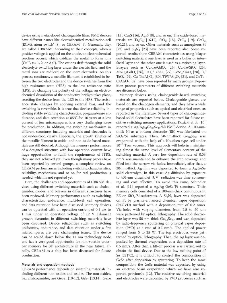
Figure 1 TEM images and EDX analysis of a Cu/Ge0.4Se0.6/W pristine memorya scale bar of 50 nm. The Ge0.4Se0.6 film shows to be amorphous, as shown inare clearly shown by the dark-field TEM image and (d) corresponding EDX an
performed to obtain the resistive switching memory de-vice. To investigate the memory device and microstructureof the solid electrolyte films, transmission electron micros-copy (TEM) was carried out using a FEI Tecnai G2F-20field emission system with an energy of 200 kV. The mem-ory devices for TEM observation were prepared using anFEI Helios-400s system with an operating voltage of 5 kVand using a Ga+ ion source. Figure 1a shows a TEM imageand energy-dispersive X-ray spectroscopy (EDX) analysisof a Cu/Ge0.4Se0.6/W structure [33]. The thicknesses ofthe Cu and W electrodes are found to be 136 and 85 nm,respectively. The thickness of the Ge0.2Se0.8 solid electro-lyte films is approximately 38 nm. A small via-hole size isabout 140 nm in width, which is lower (slightly) than ourdesign size (200 nm). The Ge0.4Se0.6 film is amorphous, asshown in the outside (Figure 1b) and inside (Figure 1c) ofthe via-hole regions. A layer-by-layer structure is observedfrom those images. All materials such as Cu, Ge, Se, andW in the Cu TE, GeSe switching, and W BE layers areconfirmed by EDX analysis (Figure 1d). Figure 2a showsthe X-ray photo-electron spectroscopy (XPS) spectra ofthe GexSe1 − x solid electrolyte films. The peak binding en-ergies of Ge0.5Se0.5, Ge0.4Se0.6, Ge0.3Se0.7, and Ge0.2Se0.8films are found to be 30.1, 30.6, 31, and 31.1 eV, respect-ively. The peak binding energy of Ge 3d electrons in-creased (30.1 to 31.1 = 1 eV) owing to increased Se
device. (a) TEM image of a Cu/Ge0.4Se0.6/W pristine memory device withthe (b) outside and (c) inside of the via-hole region. (c) Different layersalysis of the W, Ge0.4Se0.6, and Cu films from (a) [33].
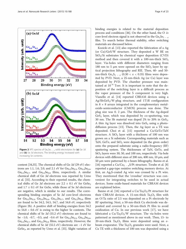
Figure 2 XPS spectra of GexSe1 − x solid electrolytes for (a) Ge 3dand (b) Se 3d electrons. The binding energy increased withincreasing Se contents.
Jana et al. Nanoscale Research Letters (2015) 10:188 Page 4 of 23
content [34,35]. The chemical shifts of Ge 3d (29 eV) elec-trons are 1.1, 1.6, 2.0, and 2.1 eV for Ge0.5Se0.5, Ge0.4Se0.6,Ge0.3Se0.7, and Ge0.2Se0.8 films, respectively. A similarchemical shift of Ge 3d electrons was reported by Uenoet al. [35]. According to their reported results, the chem-ical shifts of Ge 3d electrons are 2.2 ± 0.1 eV for GeSe2and 1.7 ± 0.1 eV for GeSe, while those of Se 3d electronsare negative, which is similar to our results. The corre-sponding binding energies of Se 3d core-level electronsfor Ge0.5Se0.5, Ge0.4Se0.6, Ge0.3Se0.7, and Ge0.2Se0.8 filmsare found to be 54.2, 54.5, 54.7, and 54.8 eV, respectively(Figure 2b). A positive shift of binding energies from 54.2to 54.8 = 0.6 eV is owing to the higher Se contents. Thechemical shifts of Se 3d (55.2 eV) electrons are found tobe −1.0, −0.7, −0.5, and −0.4 eV for Ge0.5Se0.5, Ge0.4Se0.6,Ge0.3Se0.7, and Ge0.2Se0.8 films, respectively. However, thechemical shifts of Se 3d (55.5 eV) electrons are −1 eV forGeSe2, as reported by Ueno et al. [35]. Slight variation of
binding energies is related to the material depositionprocess and conditions [36]. On the other hand, the O 1score-level electron signal is not observed in the GexSe1 − x
film. To search better thermal stability, other switchingmaterials are discussed below.Kozicki et al. [13] also reported the fabrication of a Ag
(or Cu)/GeS/W structure. They deposited a W BE onSiO2/Si substrates by chemical vapor deposition (CVD)method and then covered it with a 100-nm-thick SiO2
layer. Via-holes with different diameters ranging from180 nm to 5 μm were opened on the SiO2 layer by op-tical projection lithography and RIE. Then, 40- and 50-nm-thick GexS1 − x (0.30 < x < 0.35) films were depos-ited by PVD. Next, a 25-nm-thick Ag (or Cu) layer wasdeposited by PVD. The chamber pressure was main-tained at 10−6 Torr. It is important to note that the de-position of the switching layer is a difficult process asthe vapor pressure of the S component is very high.Vianello et al. [14] reported CBRAM devices using aAg/Sb:GeS2/W-plug structure, and 1T1R configurationin 8 × 8 arrays integrated in the complementary metal-oxide-semiconductor (CMOS) process was done. Theplug size was 0. 2 μm. The thickness of the Ag-dopedGeS2 layer, which was deposited by co-sputtering, was30 nm. The Sb material was doped 2% to 20% in GeS2.A thin Ag layer was dissolved into GeS2 using a photo-diffusion process [13]. Then, the Ag layer as a TE wasdeposited. Choi et al. [15] reported a Cu/GeTe/TaNstructure. A SiO2 layer with a thickness of 100 nm wasgrown on a Si substrate. Corresponding materials such asTaN, GeTe, and SiO2 were deposited (in the given order)onto the prepared substrate using a radio-frequency (RF)sputtering system. The thicknesses of TaN, GeTe, andSiO2 layers were 30, 50, and 100 nm, respectively. Via-holedevices with different sizes of 200 nm, 400 nm, 10 μm, and50 μm were patterned by e-beam lithography. Banno et al.[16] reported a Cu/Cu2 − αS/Pt structure. Terabe et al. [8]reported a gap-type resistive switching memory device. Atfirst, an Ag2S-coated Ag wire was crossed by a Pt wire.They mentioned that the ‘crossbar’ structure was con-venient for integrating switches to be used in actualdevices. Some oxide-based materials for CBRAM devicesare explained below.Banno et al. [16] reported a Cu/Ta2O5/Pt structure for
their CBRAM devices. A 15-nm-thick Ta2O5 film withan O/Ta ratio of 2.5 was deposited on a Pt electrode byRF sputtering. Next, a 50-nm-thick Cu electrode was de-posited and covered by a 50-nm-thick Pt film to avoidoxidization of Cu. In our previous work [17], we havefabricated a Cu/Ta2O5/W structure. The via-holes werepatterned as mentioned above in our work. Then, 15- to20-nm-thick Ta2O5 films were deposited using an e-beam evaporator. The Ta2O5 granules were used. Next, aCu TE with a thickness of 100 nm was deposited using a
Jana et al. Nanoscale Research Letters (2015) 10:188 Page 5 of 23
thermal evaporator. Finally, a lift-off process was doneto obtain the memory devices. A post metal annealingtreatment was performed at a temperature of 350°C for1 min in N2 ambient. Schindler et al. [18] reported aCu/SiO2/W structure. A 100-nm-thick W BE was depos-ited by CVD on SiO2/Si substrates. Then, a SiO2 switch-ing material with thicknesses varying from 12 to 50 nmwas grown by electron beam evaporation. A Cu TE witha thickness of 35 to 45 nm was deposited. Then, Cu wasdiffused into SiO2 by thermal annealing at 610°C to havea Cu/Cu:SiO2/W structure. Li et al. [19] fabricated a Ag/ZrO2/Au structure. First, a 50-nm-thick Ag layer wasdeposited using an electron beam evaporator. A ZrO2
film was also deposited. The vacuum pressure and thedeposition rate were 2 × 10⁻⁶ Torr and 1 Å/s, respect-ively. After that, a 50-nm-thick Au TE with differentareas such as 100 × 100 μm2 to 800 × 800 μm2 was de-posited. A GeOx switching material as CMOS compat-ible was reported by us [20]. Via-holes with size rangingfrom 0.2 × 0.2 μm2 to 8 × 8 μm2 were reported. A GeOx
film with a thickness of approximately 10 nm was thendeposited by RF sputtering. The GeOx film showed to bepolycrystalline. The chamber pressure was 2 × 10⁻⁵
Torr. The deposition power and pressure were 50 Wand 2 × 10⁻² Torr, respectively. Argon (Ar) gas with a
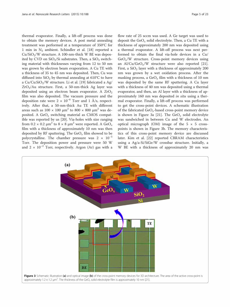
Figure 3 Schematic illustration (a) and optical image (b) of the cross-point mapproximately 1.2 × 1.2 μm2. The thickness of the GeOx solid electrolyte film is
flow rate of 25 sccm was used. A Ge target was used todeposit the GeOx solid electrolyte. Then, a Cu TE with athickness of approximately 200 nm was deposited usinga thermal evaporator. A lift-off process was next per-formed to obtain the final via-hole devices in a Cu/GeOx/W structure. Cross-point memory devices usingan Al/Cu/GeOx/W structure were also reported [21].First, a SiO2 layer with a thickness of approximately 200nm was grown by a wet oxidation process. After themasking process, a GeOx film with a thickness of 10 nmwas deposited by the same RF sputtering. A Cu layerwith a thickness of 40 nm was deposited using a thermalevaporator, and then, an Al layer with a thickness of ap-proximately 160 nm was deposited in situ using a ther-mal evaporator. Finally, a lift-off process was performedto get the cross-point devices. A schematic illustrationof the fabricated GeOx-based cross-point memory deviceis shown in Figure 3a [21]. The GeOx solid electrolytewas sandwiched in between Cu and W electrodes. Anoptical micrograph (OM) image of the 5 × 5 cross-points is shown in Figure 3b. The memory characteris-tics of this cross-point memory device are discussedlater. Kim et al. [22] reported CBRAM characteristicsusing a Ag/a-Si/SiGe/W crossbar structure. Initially, aW BE with a thickness of approximately 20 nm was
emory devices for 3D architecture. The area of the active cross-point isapproximately 10 nm [21].
Jana et al. Nanoscale Research Letters (2015) 10:188 Page 6 of 23
deposited by sputtering. In the next step, a boron-dopedSixGe1 − x film of 20 nm was deposited by thermal CVDat 425°C. An amorphous Si (a-Si) as a resistive switchingmaterial was deposited by PECVD method. The thick-ness of the a-Si film was approximately 20 nm. Finally, aAg TE was deposited. This complete stack was patternedby electron beam lithography and plasma etchingprocess. The thickness of all the layers was 50 nm half-pitch arrays. Sun et al. [23] also reported bipolarCBRAM characteristics using a Ag/Si3N4/Pt memory de-vice. The device size was 100 × 100 μm2. Even thoughmany groups reported a single-layer switching material,bilayer switching materials showed to be promising.Aratani et al. [24] investigated CBRAM characteristics
using a TE/Cu-Te/GdOx/W structure. In this case, bothTE and switching materials were deposited on the BE bya sputtering process. Device sizes of 20 and 50 nm weredesigned. The Cu-Te layer behaved as a buffer layer, andthe GdOx layer was used as a switching layer. The Cufilament formation/dissolution in the GdOx layer wascontrolled by a buffer layer through external bias. Simi-larly, Cu-Te/SiOx bilayers were also reported [25]. Yoonet al. [26] reported MoOx/GdOx bilayers in a Cu/MoOx/GdOx/Pt structure. A 10-nm-thick GdOx layer was de-posited on a Pt/Ti/SiO2/Si substrate using an electronbeam evaporator. A 100-nm-thick Pt was also deposited.After a lift-off process, a device size of 50 × 50 μm2 wasfabricated. A NanoBridge CBRAM device was reportedby using a Cu/Ta/TaSiOy/Ru structure [27]. The memorycell was integrated in the CMOS process. Via-holes withcell sizes ranging from 1 μm to 50 nm were completed.After deposition of a Ti or Ta barrier layer on Cu, aTaSiOy solid electrolyte was deposited by RF sputteringin Ar/O2 gas. The CBRAM devices were connectedthrough contact holes and controlled the switchingthrough a CMOS transistor. Therefore, the 1T1R config-uration was developed. In our previous work [28], we re-ported GeSex/TaOx bilayer materials in an Al/Cu/GeSex/TaOx/W structure. Although this CBRAM device usingGeSex/TaOx bilayers shows promising resistive switchingcharacteristics, the thermal stability of the Ge20Se80 ma-terial is an issue. To have a CMOS-compatible structure,we reported a Al/Cu/TiO2/TaOx/W CBRAM device[29]. The via-hole devices were fabricated as follows[17,28]. A Ta2O5 film with a thickness of 18 nm was de-posited from pure Ta2O5 granules using an electronbeam evaporator. The resulting Ta2O5 film was mixedwith Ta metal (i.e., TaOx, where x < 2.5), as characterizedby XPS. The Cu as mobile ions plays a major role in theAl/Cu/TaOx/W structure resistive switching memory de-vice. The Cu can be oxidized at the Cu/TaOx interfaceduring deposition and hinders the resistive switchingmemory performance. Therefore, Cu oxidation is ex-pected to be avoided by inserting a Ti nanolayer at the
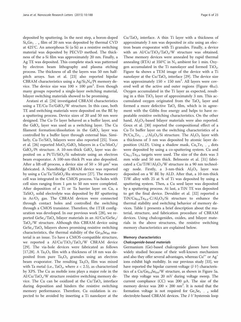
Cu/TaOx interface. A thin Ti layer with a thickness ofapproximately 3 nm was deposited in situ using an elec-tron beam evaporator with Ti granules. Finally, a devicewith an Al/Cu/TiO2/TaOx/W structure was obtained.These memory devices were annealed by rapid thermalannealing (RTA) at 350°C in N2 ambient for 1 min. Oxy-gen accumulated in the Ti nanolayer and formed TiO2.Figure 4a shows a TEM image of the device with a Tinanolayer at the Cu/TaOx interface [29]. The device sizewas approximately 150 × 150 nm2. All layers were cov-ered well at the active and outer regions (Figure 4b,c).Oxygen accumulated in the Ti layer as expected, result-ing in a thin TiO2 layer of approximately 3 nm. This ac-cumulated oxygen originated from the TaOx layer andformed a more defective TaOx film, which is in agree-ment with the Gibbs free energy and helps to have re-peatable resistive switching characteristics. On the otherhand, Al2O3-based bilayer materials were also reported.Goux et al. [30] reported the compositional effect of aCu-Te buffer layer on the switching characteristics of aPt/CuxTe1 − x/Al2O3/Si structure. The Al2O3 layer witha thickness of 3 nm was deposited by atomic layer de-position (ALD). Using a shadow mask, CuxTe1 − x dotswere deposited by using a co-sputtering system. Cu andCu0.1Te0.9 targets were used. The size of the dots was 3mm wide and 50 nm thick. Belmonte et al. [31] fabri-cated a Cu/TiW/Al2O3/W structure in a 90 nm technol-ogy node. Firstly, a 3-nm-thick Al2O3 layer wasdeposited on a W BE by ALD. After that, a 10-nm-thickTiW alloy with 25 at % of Ti was deposited by using asputtering system. Then, a Cu seed layer was depositedby a sputtering process. At last, a TiN TE was depositedto get the final device. Devulder et al. [32] reported aTiN/Cu0.6Te0.4-C/Al2O3/Si structure to enhance thethermal stability and switching behavior of memory de-vices. Table 1 presents a brief description about the ma-terial, structure, and fabrication procedure of CBRAMdevices. Using chalcogenides, oxides, and bilayer mate-rials in the above structures, the resistive switchingmemory characteristics are explained below.
Memory characteristicsChalcogenide-based materialsGermanium (Ge)-based chalcogenide glasses have beenwidely studied because of their well-known mechanismand also they offer several advantages, whereas Cuz+ or Ag+
ions exhibit high mobility. In our previous study [33], wehave reported the bipolar current-voltage (I-V) characteris-tics of a Cu/Ge0.4Se0.6/W structure, as shown in Figure 5a.The step voltage was 20 mV during voltage sweep. Thecurrent compliance (CC) was 200 μA. The size of thememory device was 200 × 200 nm2. It is noted that theformation voltage is not required for GexSe1 − x solidelectrolyte-based CBRAM devices. The I-V hysteresis loop
Figure 4 TEM image of an Al/Cu/Ti/TaOx/W structure. (a) HRTEM images of the (b) outside and (c) inside of the via-hole device, as shown in (a).After deposition of a Ti nanolayer, it became TiO2 [29].
Jana et al. Nanoscale Research Letters (2015) 10:188 Page 7 of 23
can be explained as follows by using arrows 1 to 9. Initially,a voltage applied to the TE is swept from 0 to +0.56 V(arrow 1); this is the HRS. Beyond the voltage of +0.56 V,there is an instantaneous switching from the HRS to theLRS (arrow 2). The resistive switching is observed beyond avoltage of 0.56 V, which is called SET voltage (VSET). Toform a Cu metallic filament into the Ge0.4Se0.6 solidelectrolyte, the applied bias should be larger than theSET voltage (arrow 3). The memory device keeps the
Table 1 CBRAM material and deposition methods
Device structure(TE/switching material/BE)
Deposition methods
TE Sw
Ag/Ag33Ge20Se47/Ni [10] - Eva
Ag/Ag-GeSe/Pt [11] - RF
Al/Cu/Ge0.5Se0.5/W [12] Thermal Ele
Ag or Cu/GeS/W [13] PVD PVD
Ag/Sb:GeS2/W [14] - RF
Cu/Ta2O5/Pt [16] - RF
Cu/Ta2O5/W [17] Thermal evaporator E-b
Cu/Cu:SiO2/W [18] - E-b
Ag/a-Si/SiGe/W [22] - CVD
Ag/Si3N4/Pt [23] RF sputtering PEC
Cu/Cu-Te/GdOx/W [24] Sputtering Spu
Cu/Ta/TaSiOy/Ru [27] - PEC
Al/Cu/Ti/TaOx/W [29] Thermal Ele
Cu-Te/Al2O3/Si [30] Co-sputtering ALD
Al/TiN/Cu/TiW/Al2O3/W [31] - ALD
LRS up to a negative voltage of −0.18 V (arrows 3 to 6).The resistive memory device reaches a HRS if the volt-age applied is more than the negative voltage or RESETvoltage (VRESET) < −0.16 V (arrow 7). A large RESETcurrent (IRESET) of −85 μA confirms that the strong Cumetallic filament is formed into the Ge0.4Se0.6 solid elec-trolyte. To reach a HRS, a negative voltage of −1.2 Vshould be large enough (arrow 8). The metallic filament isgradually dissolved by applying a higher negative voltage.
Devicesize (μm)itching material BE
poration - 40, 75
sputtering Thermal evaporation 2 to 50
ctron beam Sputtering 0.2 to 8.0
CVD 0.18 to 5
PVD - 0.2
sputtering - -
eam evaporation Sputtering 0.2 to 8.0
eam evaporation CVD 0.35 to 5
Sputtering 0.05
VD RF sputtering 10
ttering - 0.02, 0.05
VD - 0.05 to 1
ctron beam Sputtering 0.15
- -
Sputtering 0.09
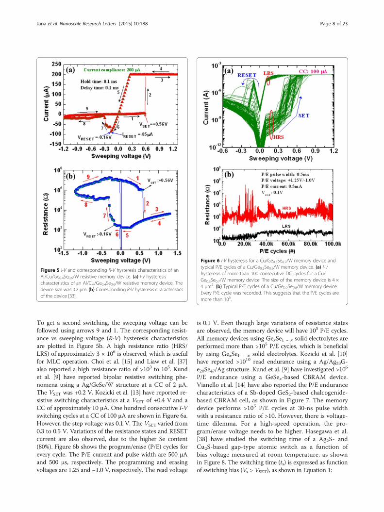
Figure 5 I-V and corresponding R-V hysteresis characteristics of anAl/Cu/Ge0.4Se0.6/W resistive memory device. (a) I-V hysteresischaracteristics of an Al/Cu/Ge0.4Se0.6/W resistive memory device. Thedevice size was 0.2 μm. (b) Corresponding R-V hysteresis characteristicsof the device [33].
Figure 6 I-V hysteresis for a Cu/Ge0.3Se0.7/W memory device andtypical P/E cycles of a Cu/Ge0.2Se0.8/W memory device. (a) I-Vhysteresis of more than 100 consecutive DC cycles for a Cu/Ge0.3Se0.7/W memory device. The size of the memory device is 4 ×4 μm2. (b) Typical P/E cycles of a Cu/Ge0.2Se0.8/W memory device.Every P/E cycle was recorded. This suggests that the P/E cycles aremore than 105.
Jana et al. Nanoscale Research Letters (2015) 10:188 Page 8 of 23
To get a second switching, the sweeping voltage can befollowed using arrows 9 and 1. The corresponding resist-ance vs sweeping voltage (R-V) hysteresis characteristicsare plotted in Figure 5b. A high resistance ratio (HRS/LRS) of approximately 3 × 10⁶ is observed, which is usefulfor MLC operation. Choi et al. [15] and Liaw et al. [37]also reported a high resistance ratio of >103 to 105. Kundet al. [9] have reported bipolar resistive switching phe-nomena using a Ag/GeSe/W structure at a CC of 2 μA.The VSET was +0.2 V. Kozicki et al. [13] have reported re-sistive switching characteristics at a VSET of +0.4 V and aCC of approximately 10 μA. One hundred consecutive I-Vswitching cycles at a CC of 100 μA are shown in Figure 6a.However, the step voltage was 0.1 V. The VSET varied from0.3 to 0.5 V. Variations of the resistance states and RESETcurrent are also observed, due to the higher Se content(80%). Figure 6b shows the program/erase (P/E) cycles forevery cycle. The P/E current and pulse width are 500 μAand 500 μs, respectively. The programming and erasingvoltages are 1.25 and −1.0 V, respectively. The read voltage
is 0.1 V. Even though large variations of resistance statesare observed, the memory device will have 105 P/E cycles.All memory devices using GexSe1 − x solid electrolytes areperformed more than >105 P/E cycles, which is beneficialby using GexSe1 − x solid electrolytes. Kozicki et al. [10]have reported >1010 read endurance using a Ag/Ag33G-e20Se47/Ag structure. Kund et al. [9] have investigated >106
P/E endurance using a GeSex-based CBRAM device.Vianello et al. [14] have also reported the P/E endurancecharacteristics of a Sb-doped GeS2-based chalcogenide-based CBRAM cell, as shown in Figure 7. The memorydevice performs >105 P/E cycles at 30-ns pulse widthwith a resistance ratio of >10. However, there is voltage-time dilemma. For a high-speed operation, the pro-gram/erase voltage needs to be higher. Hasegawa et al.[38] have studied the switching time of a Ag2S- andCu2S-based gap-type atomic switch as a function ofbias voltage measured at room temperature, as shownin Figure 8. The switching time (ts) is expressed as functionof switching bias (Vs > VSET), as shown in Equation 1:
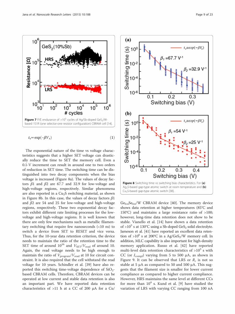
Figure 7 P/E endurance of >105 cycles of Ag/Sb-doped GeS2/W-based 1S1R (one selector-one resistor configuration) CBRAM cell [14].
Figure 8 Switching time vs switching bias characteristics. For (a)Ag2S-based gap-type atomic switch at room temperature and (b)Cu2S-based gap-type atomic switch [38].
Jana et al. Nanoscale Research Letters (2015) 10:188 Page 9 of 23
ts∞ exp −βV sð Þ ð1Þ
The exponential nature of the time vs voltage charac-teristics suggests that a higher SET voltage can drastic-ally reduce the time to SET the memory cell. Even a0.1-V increment can result in around one to two ordersof reduction in SET time. The switching time can be dis-tinguished into two decay components when the biasvoltage is increased (Figure 8a). The values of decay fac-tors β1 and β2 are 67.7 and 32.9 for low-voltage andhigh-voltage regions, respectively. Similar phenomenaare also reported in a Cu2S switching material, as shownin Figure 8b. In this case, the values of decay factors β1and β2 are 54 and 25 for low-voltage and high-voltageregions, respectively. These two exponential decay fac-tors exhibit different rate limiting processes for the low-voltage and high-voltage regions. It is well known thatthere are only few mechanisms such as metallic filamen-tary switching that require few nanoseconds (<10 ns) toswitch a device from SET to RESET and vice versa.Thus, for the 10-year data retention criterion, the deviceneeds to maintain the ratio of the retention time to theSET time of around 1016 and VSET/Vread of around 10.Again, the read voltage needs to be high enough tomaintain the ratio of Vprogram/Vread at 10 for circuit con-straint. It is also required that the cell withstand the readvoltage for 10 years. Schindler et al. [39] have also re-ported this switching time-voltage dependence of SiO2-based CBRAM cells. Therefore, CBRAM devices can beoperated at low current and stable data retention is alsoan important part. We have reported data retentioncharacteristics of >11 h at a CC of 200 μA for a Cu/
Ge0.4Se0.6/W CBRAM device [40]. The memory deviceshows data retention at higher temperatures (85°C and150°C) and maintains a large resistance ratio of >100;however, long-time data retention does not show to bestable. Vianello et al. [14] have shown a data retentionof >105 s at 130°C using a Sb-doped GeS2 solid electrolyte.Jameson et al. [41] have reported an excellent data reten-tion of >106 s at 200°C in a Ag/GeS2/W memory cell. Inaddition, MLC capability is also important for high-densitymemory application. Russo et al. [42] have reportedmulti-level data retention characteristics of >105 s withCC (or Icompl) varying from 5 to 500 μA, as shown inFigure 9. It can be observed that LRS or Rc is not sostable at 5 μA as compared to 50 and 500 μA. This sug-gests that the filament size is smaller for lower currentcompliance as compared to higher current compliance.However, HRS maintains the same level at different CCsfor more than 104 s. Kund et al. [9] have studied thevariation of LRS with varying CC ranging from 100 nA
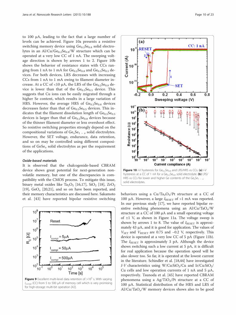
Figure 10 I-V hysteresis for Ge0.2Se0.8 and LRS/HRS vs CCs. (a) I-Vhysteresis at a CC of 1 nA for a Ge0.2Se0.8 solid electrolyte. (b) LRS/HRS vs CCs for lower and higher Ge contents of the GexSe1 − x
solid electrolytes.
Jana et al. Nanoscale Research Letters (2015) 10:188 Page 10 of 23
to 100 μA, leading to the fact that a large number oflevels can be achieved. Figure 10a presents a resistiveswitching memory device using Ge0.2Se0.8 solid electro-lytes in an Al/Cu/Ge0.2Se0.8/W structure which can beoperated at a very low CC of 1 nA. The sweeping volt-age direction is shown by arrows 1 to 2. Figure 10bshows the behavior of resistance states with CCs ran-ging from 1 nA to 1 mA for Ge0.2Se0.8 and Ge0.5Se0.5 de-vices. For both devices, LRS decreases with increasingCCs from 1 nA to 1 mA owing to filament diameter in-crease. At a CC of <10 μA, the LRS of the Ge0.2Se0.8 de-vice is lower than that of the Ge0.5Se0.5 device. Thissuggests that Cu ions can be easily migrated through ahigher Se content, which results in a large variation ofHRS. However, the average HRS of Ge0.2Se0.8 devicesdecreases faster than that of Ge0.5Se0.5 devices. This in-dicates that the filament dissolution length of Ge0.5Se0.5devices is larger than that of Ge0.2Se0.8 devices becauseof the thinner filament diameter or less overshoot effect.So resistive switching properties strongly depend on thecompositional variations of GexSe1 − x solid electrolytes.However, the SET voltage, endurance, data retention,and so on may be controlled using different composi-tions of GeSex solid electrolytes as per the requirementof the applications.
Oxide-based materialsIt is observed that the chalcogenide-based CBRAMdevice shows great potential for next-generation non-volatile memory, but one of the discrepancies is com-patibility with the CMOS process. To mitigate this issue,binary metal oxides like Ta2O5 [16,17], SiO2 [18], ZrO2
[19], GeOx [20,21], and so on have been reported, andtheir memory characteristics are discussed here. Sakamotoet al. [43] have reported bipolar resistive switching
Figure 9 Excellent multi-level data retention of >105 s. With varyingIcompl (CC) from 5 to 500 μA of memory cell which is very promisingfor high-storage multi-bit operation [42].
behaviors using a Cu/Ta2O5/Pt structure at a CC of100 μA. However, a large IRESET of >1 mA was reported.In our previous study [17], we have reported bipolar re-sistive switching phenomena using an Al/Cu/TaOx/Wstructure at a CC of 100 μA and a small operating voltageof ±1 V, as shown in Figure 11a. The voltage sweep isshown by arrows 1 to 8. The value of IRESET is approxi-mately 43 μA, and it is good for application. The values ofVSET and VRESET are 0.75 and −0.2 V, respectively. Thisdevice is operated at a very low CC of 5 pA (Figure 11b).The IRESET is approximately 3 pA. Although the deviceshows switching such a low current at 5 pA, it is difficultfor real application because the operation speed will bealso slower too. So far, it is operated at the lowest currentin the literature. Schindler et al. [18,44] have investigatedI-V characteristics using W/Cu:SiO2/Cu and Ir/Cu:SiO2/Cu cells and low operation currents of 1 nA and 5 μA,respectively. Tsunoda et al. [45] have reported CBRAMphenomena using a Ag/TiO2/Pt structure at a CC of100 μA. Statistical distribution of the HRS and LRS ofAl/Cu/TaOx/W memory devices shows also to be good
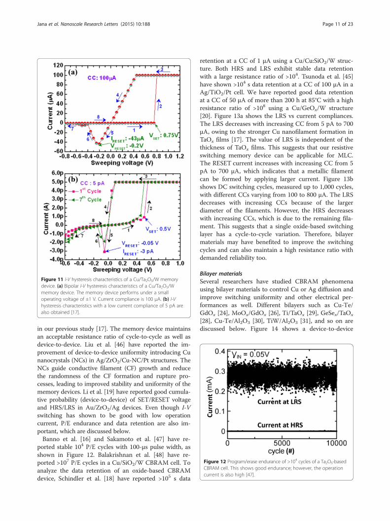
Figure 11 I-V hysteresis characteristics of a Cu/Ta2O5/W memorydevice. (a) Bipolar I-V hysteresis characteristics of a Cu/Ta2O5/Wmemory device. The memory device performs under a smalloperating voltage of ±1 V. Current compliance is 100 μA. (b) I-Vhysteresis characteristics with a low current compliance of 5 pA arealso obtained [17].
Figure 12 Program/erase endurance of >104 cycles of a Ta2O5-basedCBRAM cell. This shows good endurance; however, the operationcurrent is also high [47].
Jana et al. Nanoscale Research Letters (2015) 10:188 Page 11 of 23
in our previous study [17]. The memory device maintainsan acceptable resistance ratio of cycle-to-cycle as well asdevice-to-device. Liu et al. [46] have reported the im-provement of device-to-device uniformity introducing Cunanocrystals (NCs) in Ag/ZrO2/Cu-NC/Pt structures. TheNCs guide conductive filament (CF) growth and reducethe randomness of the CF formation and rupture pro-cesses, leading to improved stability and uniformity of thememory devices. Li et al. [19] have reported good cumula-tive probability (device-to-device) of SET/RESET voltageand HRS/LRS in Au/ZrO2/Ag devices. Even though I-Vswitching has shown to be good with low operationcurrent, P/E endurance and data retention are also im-portant, which are discussed below.Banno et al. [16] and Sakamoto et al. [47] have re-
ported stable 104 P/E cycles with 100-μs pulse width, asshown in Figure 12. Balakrishnan et al. [48] have re-ported >107 P/E cycles in a Cu/SiO2/W CBRAM cell. Toanalyze the data retention of an oxide-based CBRAMdevice, Schindler et al. [18] have reported >105 s data
retention at a CC of 1 μA using a Cu/Cu:SiO2/W struc-ture. Both HRS and LRS exhibit stable data retentionwith a large resistance ratio of >104. Tsunoda et al. [45]have shown >104 s data retention at a CC of 100 μA in aAg/TiO2/Pt cell. We have reported good data retentionat a CC of 50 μA of more than 200 h at 85°C with a highresistance ratio of >108 using a Cu/GeOx/W structure[20]. Figure 13a shows the LRS vs current compliances.The LRS decreases with increasing CC from 5 pA to 700μA, owing to the stronger Cu nanofilament formation inTaOx films [17]. The value of LRS is independent of thethickness of TaOx films. This suggests that our resistiveswitching memory device can be applicable for MLC.The RESET current increases with increasing CC from 5pA to 700 μA, which indicates that a metallic filamentcan be formed by applying larger current. Figure 13bshows DC switching cycles, measured up to 1,000 cycles,with different CCs varying from 100 to 800 μA. The LRSdecreases with increasing CCs because of the largerdiameter of the filaments. However, the HRS decreaseswith increasing CCs, which is due to the remaining fila-ment. This suggests that a single oxide-based switchinglayer has a cycle-to-cycle variation. Therefore, bilayermaterials may have benefited to improve the switchingcycles and can also maintain a high resistance ratio withdemanded reliability too.
Bilayer materialsSeveral researchers have studied CBRAM phenomenausing bilayer materials to control Cu or Ag diffusion andimprove switching uniformity and other electrical per-formances as well. Different bilayers such as Cu-Te/GdOx [24], MoOx/GdOx [26], Ti/TaOx [29], GeSex/TaOx
[28], Cu-Te/Al2O3 [30], TiW/Al2O3 [31], and so on arediscussed below. Figure 14 shows a device-to-device
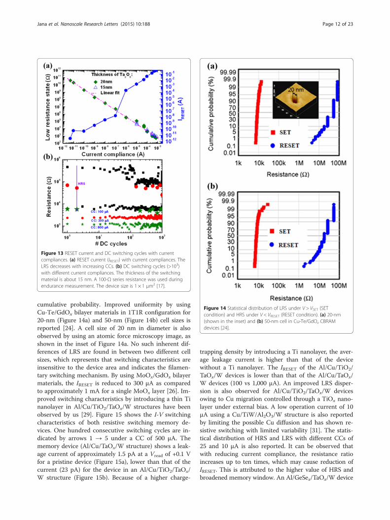
Figure 13 RESET current and DC switching cycles with currentcompliances. (a) RESET current (IRESET) with current compliances. TheLRS decreases with increasing CCs. (b) DC switching cycles (>103)with different current compliances. The thickness of the switchingmaterial is about 15 nm. A 100-Ω series resistance was used duringendurance measurement. The device size is 1 × 1 μm2 [17].
Figure 14 Statistical distribution of LRS under V > VSET (SETcondition) and HRS under V < VRESET (RESET condition). (a) 20-nm(shown in the inset) and (b) 50-nm cell in Cu-Te/GdOx CBRAMdevices [24].
Jana et al. Nanoscale Research Letters (2015) 10:188 Page 12 of 23
cumulative probability. Improved uniformity by usingCu-Te/GdOx bilayer materials in 1T1R configuration for20-nm (Figure 14a) and 50-nm (Figure 14b) cell sizes isreported [24]. A cell size of 20 nm in diameter is alsoobserved by using an atomic force microscopy image, asshown in the inset of Figure 14a. No such inherent dif-ferences of LRS are found in between two different cellsizes, which represents that switching characteristics areinsensitive to the device area and indicates the filamen-tary switching mechanism. By using MoOx/GdOx bilayermaterials, the IRESET is reduced to 300 μA as comparedto approximately 1 mA for a single MoOx layer [26]. Im-proved switching characteristics by introducing a thin Tinanolayer in Al/Cu/TiO2/TaOx/W structures have beenobserved by us [29]. Figure 15 shows the I-V switchingcharacteristics of both resistive switching memory de-vices. One hundred consecutive switching cycles are in-dicated by arrows 1 → 5 under a CC of 500 μA. Thememory device (Al/Cu/TaOx/W structure) shows a leak-age current of approximately 1.5 pA at a Vread of +0.1 Vfor a pristine device (Figure 15a), lower than that of thecurrent (23 pA) for the device in an Al/Cu/TiO2/TaOx/W structure (Figure 15b). Because of a higher charge-
trapping density by introducing a Ti nanolayer, the aver-age leakage current is higher than that of the devicewithout a Ti nanolayer. The IRESET of the Al/Cu/TiO2/TaOx/W devices is lower than that of the Al/Cu/TaOx/W devices (100 vs 1,000 μA). An improved LRS disper-sion is also observed for Al/Cu/TiO2/TaOx/W devicesowing to Cu migration controlled through a TiOx nano-layer under external bias. A low operation current of 10μA using a Cu/TiW/Al2O3/W structure is also reportedby limiting the possible Cu diffusion and has shown re-sistive switching with limited variability [31]. The statis-tical distribution of HRS and LRS with different CCs of25 and 10 μA is also reported. It can be observed thatwith reducing current compliance, the resistance ratioincreases up to ten times, which may cause reduction ofIRESET. This is attributed to the higher value of HRS andbroadened memory window. An Al/GeSex/TaOx/W device
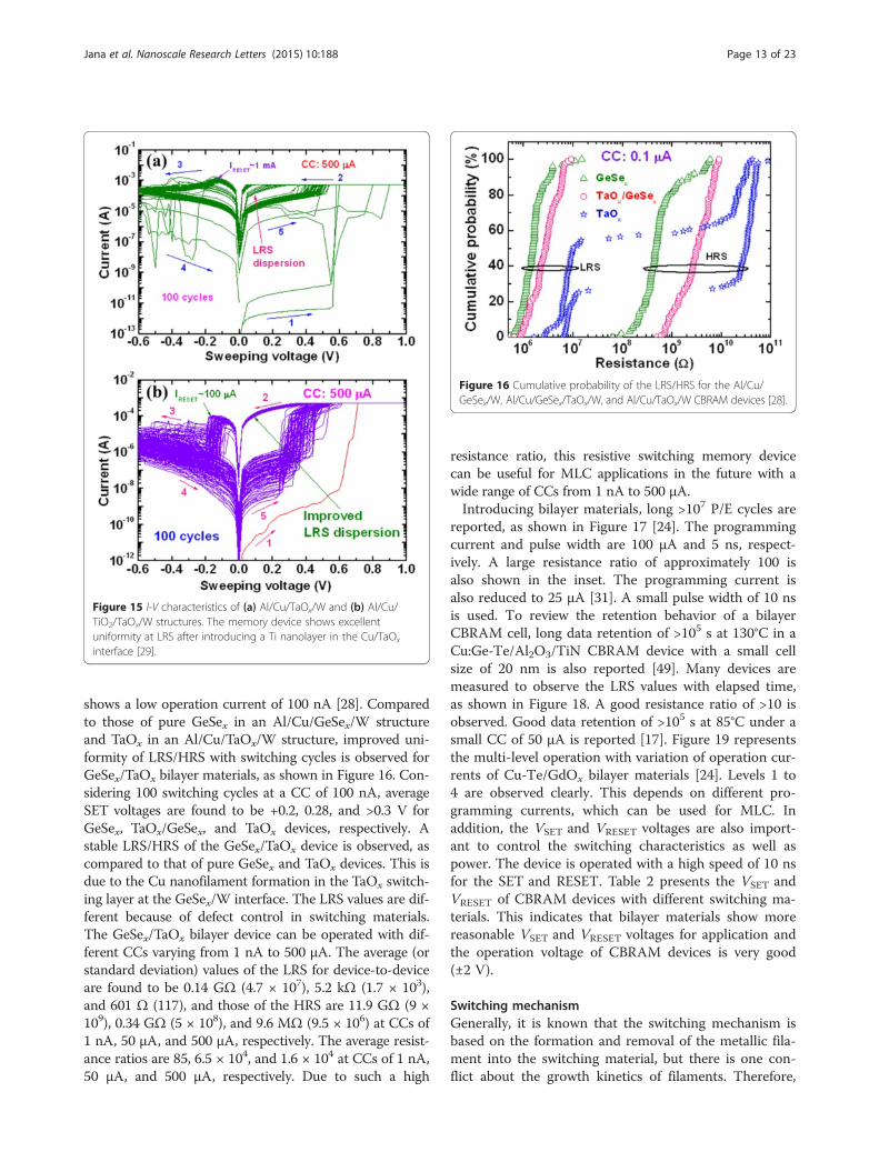
Figure 15 I-V characteristics of (a) Al/Cu/TaOx/W and (b) Al/Cu/TiO2/TaOx/W structures. The memory device shows excellentuniformity at LRS after introducing a Ti nanolayer in the Cu/TaOx
interface [29].
Figure 16 Cumulative probability of the LRS/HRS for the Al/Cu/GeSex/W, Al/Cu/GeSex/TaOx/W, and Al/Cu/TaOx/W CBRAM devices [28].
Jana et al. Nanoscale Research Letters (2015) 10:188 Page 13 of 23
shows a low operation current of 100 nA [28]. Comparedto those of pure GeSex in an Al/Cu/GeSex/W structureand TaOx in an Al/Cu/TaOx/W structure, improved uni-formity of LRS/HRS with switching cycles is observed forGeSex/TaOx bilayer materials, as shown in Figure 16. Con-sidering 100 switching cycles at a CC of 100 nA, averageSET voltages are found to be +0.2, 0.28, and >0.3 V forGeSex, TaOx/GeSex, and TaOx devices, respectively. Astable LRS/HRS of the GeSex/TaOx device is observed, ascompared to that of pure GeSex and TaOx devices. This isdue to the Cu nanofilament formation in the TaOx switch-ing layer at the GeSex/W interface. The LRS values are dif-ferent because of defect control in switching materials.The GeSex/TaOx bilayer device can be operated with dif-ferent CCs varying from 1 nA to 500 μA. The average (orstandard deviation) values of the LRS for device-to-deviceare found to be 0.14 GΩ (4.7 × 10⁷), 5.2 kΩ (1.7 × 10³),and 601 Ω (117), and those of the HRS are 11.9 GΩ (9 ×10⁹), 0.34 GΩ (5 × 10⁸), and 9.6 MΩ (9.5 × 10⁶) at CCs of1 nA, 50 μA, and 500 μA, respectively. The average resist-ance ratios are 85, 6.5 × 10⁴, and 1.6 × 10⁴ at CCs of 1 nA,50 μA, and 500 μA, respectively. Due to such a high
resistance ratio, this resistive switching memory devicecan be useful for MLC applications in the future with awide range of CCs from 1 nA to 500 μA.Introducing bilayer materials, long >107 P/E cycles are
reported, as shown in Figure 17 [24]. The programmingcurrent and pulse width are 100 μA and 5 ns, respect-ively. A large resistance ratio of approximately 100 isalso shown in the inset. The programming current isalso reduced to 25 μA [31]. A small pulse width of 10 nsis used. To review the retention behavior of a bilayerCBRAM cell, long data retention of >105 s at 130°C in aCu:Ge-Te/Al2O3/TiN CBRAM device with a small cellsize of 20 nm is also reported [49]. Many devices aremeasured to observe the LRS values with elapsed time,as shown in Figure 18. A good resistance ratio of >10 isobserved. Good data retention of >105 s at 85°C under asmall CC of 50 μA is reported [17]. Figure 19 representsthe multi-level operation with variation of operation cur-rents of Cu-Te/GdOx bilayer materials [24]. Levels 1 to4 are observed clearly. This depends on different pro-gramming currents, which can be used for MLC. Inaddition, the VSET and VRESET voltages are also import-ant to control the switching characteristics as well aspower. The device is operated with a high speed of 10 nsfor the SET and RESET. Table 2 presents the VSET andVRESET of CBRAM devices with different switching ma-terials. This indicates that bilayer materials show morereasonable VSET and VRESET voltages for application andthe operation voltage of CBRAM devices is very good(±2 V).
Switching mechanismGenerally, it is known that the switching mechanism isbased on the formation and removal of the metallic fila-ment into the switching material, but there is one con-flict about the growth kinetics of filaments. Therefore,

Figure 17 Pulse endurance of >107 cycles of a Cu-Te/GdOx/Wdevice. The pulse width was 10 ns. Every cycle up to 105 is shown inthe inset [24].
Figure 19 Four-level operations are shown by applying differentoperation currents. The first three levels are the SET with differentprogramming currents, and the fourth level is the RESET condition.Pulse widths for SET/RESET are 10 ns/10 ns, respectively [24].
Table 2 SET and RESET voltages (VSET and VRESET) forvarious switching materials
Reference +VSET (V) −VRESET (V)
[9] 0.25 0.08
[10] 0.2 0.1
[11] 0.2 0.05
[12] 0.75 0.03
Jana et al. Nanoscale Research Letters (2015) 10:188 Page 14 of 23
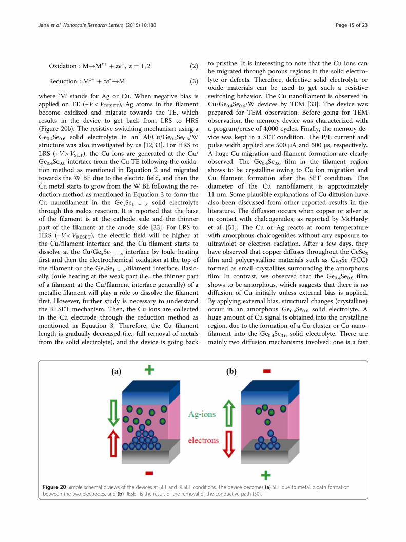
filament formation/dissolution needs to be understoodclearly for the mass production of CBRAM devices.When a positive bias is applied on the active electrodewhere the BE is grounded, then the Cu or Ag atoms areionized and drift through the switching medium (solidelectrolytes or oxide) under the electric field and finallyreach the inert electrode. The filament formation/re-moval mechanism is reported first using a Ag0.33G-e0.20Se0.47 solid electrolyte material, as shown inFigure 20 [50]. Symanczyk et al. used Ag and Au as ac-tive and inert electrodes, respectively. Under positivebias on the Ag electrode (+V >VSET), Ag atoms becomeelectrically oxidized and drift through the Ag0.33G-e0.20Se0.47 solid electrolyte and finally reduce at the AuBE due to incoming electrons from the BE. As a result,
Figure 18 Good data retention characteristics of >105 s at 130°C ofa Cu:Ge-Te/Al2O3/TiN CBRAM device [49].
the metallic filament forms due to the gradual processand the memory device switches from HRS to LRS,which is known as the SET process (Figure 20a).Ionization equations for the redox (reduction and oxida-tion) reaction are as follows:
[13] 0.3 0.3
[14] 0.3 0.2
[16] 0.15 0.1
[17] 0.75 0.2
[18] 0.9 0.15
[20] 0.6 0.2
[23] 0.5 0.25
[24] 1.0 0.75
[26] 1.1 0.7
[29] 0.6 0.15
[30] 0.5 0.3
[31] 1.5 1.0
[33] 0.56 0.16
[42] 0.4 0.2
[46] 0.5 0.2
[49] 0.7 0.5
Jana et al. Nanoscale Research Letters (2015) 10:188 Page 15 of 23
Oxidation : M→Mzþ þ ze−; z ¼ 1; 2 ð2Þ
Reduction : Mzþ þ ze−→M ð3Þ
where ‘M’ stands for Ag or Cu. When negative bias isapplied on TE (−V <VRESET), Ag atoms in the filamentbecome oxidized and migrate towards the TE, whichresults in the device to get back from LRS to HRS(Figure 20b). The resistive switching mechanism using aGe0.4Se0.6 solid electrolyte in an Al/Cu/Ge0.4Se0.6/Wstructure was also investigated by us [12,33]. For HRS toLRS (+V >VSET), the Cu ions are generated at the Cu/Ge0.4Se0.6 interface from the Cu TE following the oxida-tion method as mentioned in Equation 2 and migratedtowards the W BE due to the electric field, and then theCu metal starts to grow from the W BE following the re-duction method as mentioned in Equation 3 to form theCu nanofilament in the GexSe1 − x solid electrolytethrough this redox reaction. It is reported that the baseof the filament is at the cathode side and the thinnerpart of the filament at the anode side [33]. For LRS toHRS (−V <VRESET), the electric field will be higher atthe Cu/filament interface and the Cu filament starts todissolve at the Cu/GexSe1 − x interface by Joule heatingfirst and then the electrochemical oxidation at the top ofthe filament or the GexSe1 − x/filament interface. Basic-ally, Joule heating at the weak part (i.e., the thinner partof a filament at the Cu/filament interface generally) of ametallic filament will play a role to dissolve the filamentfirst. However, further study is necessary to understandthe RESET mechanism. Then, the Cu ions are collectedin the Cu electrode through the reduction method asmentioned in Equation 3. Therefore, the Cu filamentlength is gradually decreased (i.e., full removal of metalsfrom the solid electrolyte), and the device is going back
Figure 20 Simple schematic views of the devices at SET and RESET conditbetween the two electrodes, and (b) RESET is the result of the removal of
to pristine. It is interesting to note that the Cu ions canbe migrated through porous regions in the solid electro-lyte or defects. Therefore, defective solid electrolyte oroxide materials can be used to get such a resistiveswitching behavior. The Cu nanofilament is observed inCu/Ge0.4Se0.6/W devices by TEM [33]. The device wasprepared for TEM observation. Before going for TEMobservation, the memory device was characterized witha program/erase of 4,000 cycles. Finally, the memory de-vice was kept in a SET condition. The P/E current andpulse width applied are 500 μA and 500 μs, respectively.A huge Cu migration and filament formation are clearlyobserved. The Ge0.4Se0.6 film in the filament regionshows to be crystalline owing to Cu ion migration andCu filament formation after the SET condition. Thediameter of the Cu nanofilament is approximately11 nm. Some plausible explanations of Cu diffusion havealso been discussed from other reported results in theliterature. The diffusion occurs when copper or silver isin contact with chalcogenides, as reported by McHardyet al. [51]. The Cu or Ag reacts at room temperaturewith amorphous chalcogenides without any exposure toultraviolet or electron radiation. After a few days, theyhave observed that copper diffuses throughout the GeSe2film and polycrystalline materials such as Cu2Se (FCC)formed as small crystallites surrounding the amorphousfilm. In contrast, we observed that the Ge0.4Se0.6 filmshows to be amorphous, which suggests that there is nodiffusion of Cu initially unless external bias is applied.By applying external bias, structural changes (crystalline)occur in an amorphous Ge0.4Se0.6 solid electrolyte. Ahuge amount of Cu signal is obtained into the crystallineregion, due to the formation of a Cu cluster or Cu nano-filament into the Ge0.4Se0.6 solid electrolyte. There aremainly two diffusion mechanisms involved: one is a fast
ions. The device becomes (a) SET due to metallic path formationthe conductive path [50].
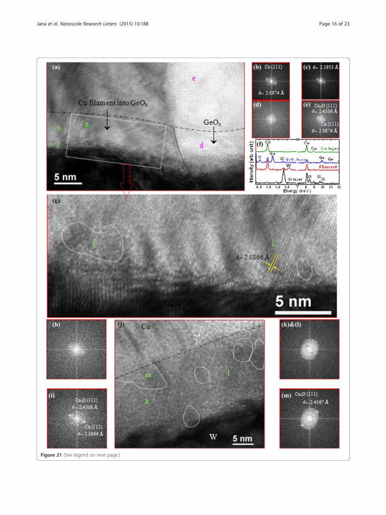
Figure 21 (See legend on next page.)
Jana et al. Nanoscale Research Letters (2015) 10:188 Page 16 of 23
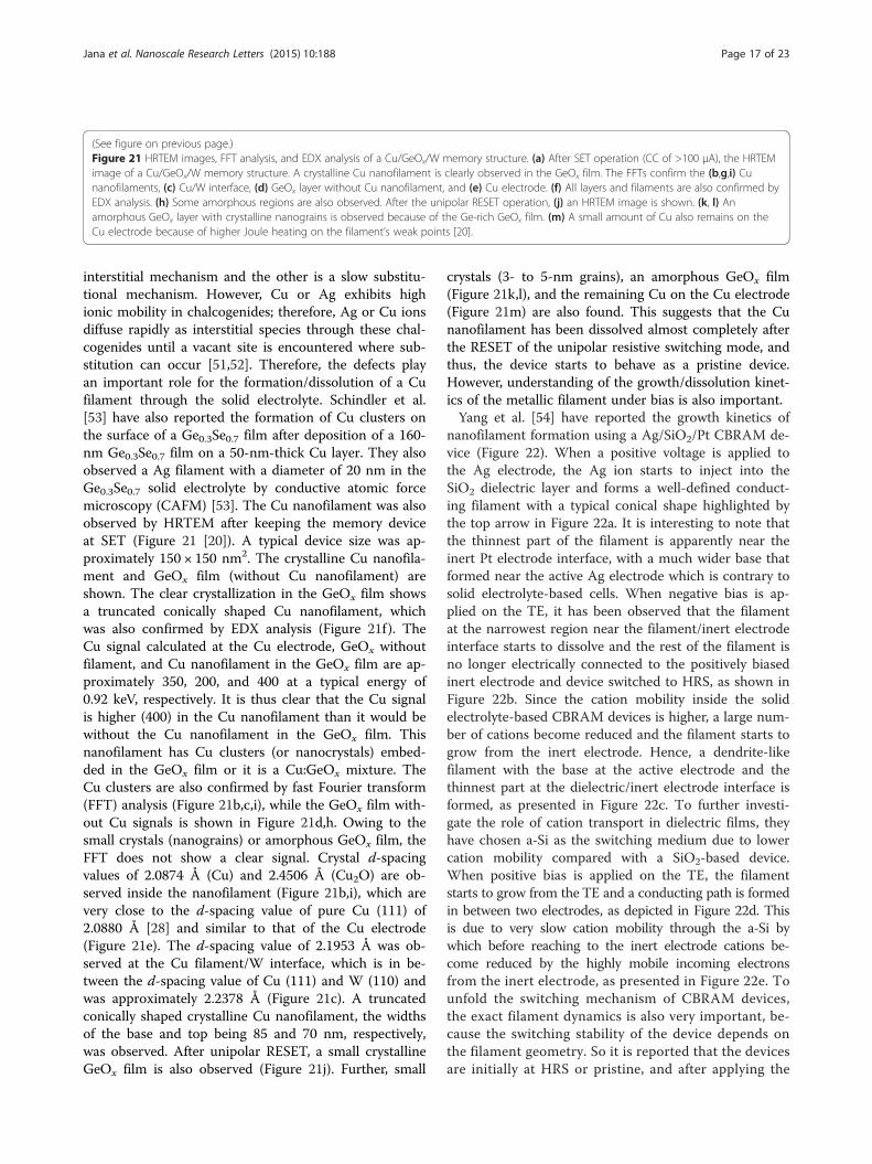
(See figure on previous page.)Figure 21 HRTEM images, FFT analysis, and EDX analysis of a Cu/GeOx/W memory structure. (a) After SET operation (CC of >100 μA), the HRTEMimage of a Cu/GeOx/W memory structure. A crystalline Cu nanofilament is clearly observed in the GeOx film. The FFTs confirm the (b,g,i) Cunanofilaments, (c) Cu/W interface, (d) GeOx layer without Cu nanofilament, and (e) Cu electrode. (f) All layers and filaments are also confirmed byEDX analysis. (h) Some amorphous regions are also observed. After the unipolar RESET operation, (j) an HRTEM image is shown. (k, l) Anamorphous GeOx layer with crystalline nanograins is observed because of the Ge-rich GeOx film. (m) A small amount of Cu also remains on theCu electrode because of higher Joule heating on the filament’s weak points [20].
Jana et al. Nanoscale Research Letters (2015) 10:188 Page 17 of 23
interstitial mechanism and the other is a slow substitu-tional mechanism. However, Cu or Ag exhibits highionic mobility in chalcogenides; therefore, Ag or Cu ionsdiffuse rapidly as interstitial species through these chal-cogenides until a vacant site is encountered where sub-stitution can occur [51,52]. Therefore, the defects playan important role for the formation/dissolution of a Cufilament through the solid electrolyte. Schindler et al.[53] have also reported the formation of Cu clusters onthe surface of a Ge0.3Se0.7 film after deposition of a 160-nm Ge0.3Se0.7 film on a 50-nm-thick Cu layer. They alsoobserved a Ag filament with a diameter of 20 nm in theGe0.3Se0.7 solid electrolyte by conductive atomic forcemicroscopy (CAFM) [53]. The Cu nanofilament was alsoobserved by HRTEM after keeping the memory deviceat SET (Figure 21 [20]). A typical device size was ap-proximately 150 × 150 nm2. The crystalline Cu nanofila-ment and GeOx film (without Cu nanofilament) areshown. The clear crystallization in the GeOx film showsa truncated conically shaped Cu nanofilament, whichwas also confirmed by EDX analysis (Figure 21f ). TheCu signal calculated at the Cu electrode, GeOx withoutfilament, and Cu nanofilament in the GeOx film are ap-proximately 350, 200, and 400 at a typical energy of0.92 keV, respectively. It is thus clear that the Cu signalis higher (400) in the Cu nanofilament than it would bewithout the Cu nanofilament in the GeOx film. Thisnanofilament has Cu clusters (or nanocrystals) embed-ded in the GeOx film or it is a Cu:GeOx mixture. TheCu clusters are also confirmed by fast Fourier transform(FFT) analysis (Figure 21b,c,i), while the GeOx film with-out Cu signals is shown in Figure 21d,h. Owing to thesmall crystals (nanograins) or amorphous GeOx film, theFFT does not show a clear signal. Crystal d-spacingvalues of 2.0874 Å (Cu) and 2.4506 Å (Cu2O) are ob-served inside the nanofilament (Figure 21b,i), which arevery close to the d-spacing value of pure Cu (111) of2.0880 Å [28] and similar to that of the Cu electrode(Figure 21e). The d-spacing value of 2.1953 Å was ob-served at the Cu filament/W interface, which is in be-tween the d-spacing value of Cu (111) and W (110) andwas approximately 2.2378 Å (Figure 21c). A truncatedconically shaped crystalline Cu nanofilament, the widthsof the base and top being 85 and 70 nm, respectively,was observed. After unipolar RESET, a small crystallineGeOx film is also observed (Figure 21j). Further, small
crystals (3- to 5-nm grains), an amorphous GeOx film(Figure 21k,l), and the remaining Cu on the Cu electrode(Figure 21m) are also found. This suggests that the Cunanofilament has been dissolved almost completely afterthe RESET of the unipolar resistive switching mode, andthus, the device starts to behave as a pristine device.However, understanding of the growth/dissolution kinet-ics of the metallic filament under bias is also important.Yang et al. [54] have reported the growth kinetics of
nanofilament formation using a Ag/SiO2/Pt CBRAM de-vice (Figure 22). When a positive voltage is applied tothe Ag electrode, the Ag ion starts to inject into theSiO2 dielectric layer and forms a well-defined conduct-ing filament with a typical conical shape highlighted bythe top arrow in Figure 22a. It is interesting to note thatthe thinnest part of the filament is apparently near theinert Pt electrode interface, with a much wider base thatformed near the active Ag electrode which is contrary tosolid electrolyte-based cells. When negative bias is ap-plied on the TE, it has been observed that the filamentat the narrowest region near the filament/inert electrodeinterface starts to dissolve and the rest of the filament isno longer electrically connected to the positively biasedinert electrode and device switched to HRS, as shown inFigure 22b. Since the cation mobility inside the solidelectrolyte-based CBRAM devices is higher, a large num-ber of cations become reduced and the filament starts togrow from the inert electrode. Hence, a dendrite-likefilament with the base at the active electrode and thethinnest part at the dielectric/inert electrode interface isformed, as presented in Figure 22c. To further investi-gate the role of cation transport in dielectric films, theyhave chosen a-Si as the switching medium due to lowercation mobility compared with a SiO2-based device.When positive bias is applied on the TE, the filamentstarts to grow from the TE and a conducting path is formedin between two electrodes, as depicted in Figure 22d. Thisis due to very slow cation mobility through the a-Si bywhich before reaching to the inert electrode cations be-come reduced by the highly mobile incoming electronsfrom the inert electrode, as presented in Figure 22e. Tounfold the switching mechanism of CBRAM devices,the exact filament dynamics is also very important, be-cause the switching stability of the device depends onthe filament geometry. So it is reported that the devicesare initially at HRS or pristine, and after applying the
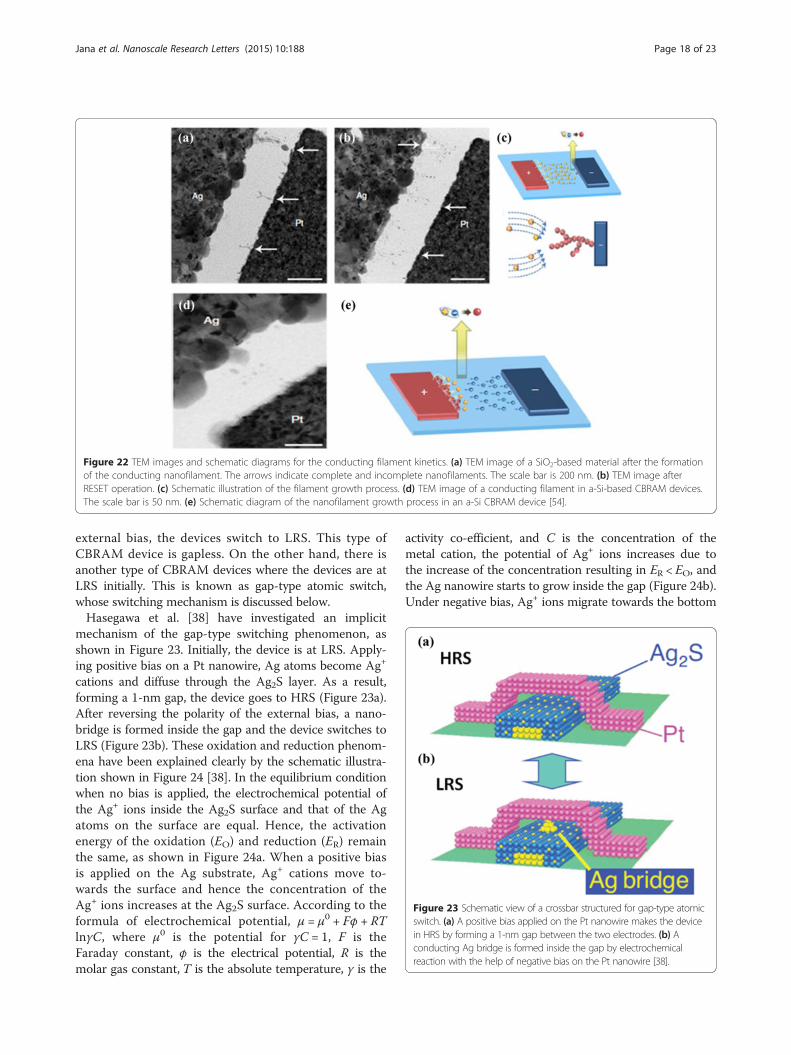
Figure 22 TEM images and schematic diagrams for the conducting filament kinetics. (a) TEM image of a SiO2-based material after the formationof the conducting nanofilament. The arrows indicate complete and incomplete nanofilaments. The scale bar is 200 nm. (b) TEM image afterRESET operation. (c) Schematic illustration of the filament growth process. (d) TEM image of a conducting filament in a-Si-based CBRAM devices.The scale bar is 50 nm. (e) Schematic diagram of the nanofilament growth process in an a-Si CBRAM device [54].
Figure 23 Schematic view of a crossbar structured for gap-type atomicswitch. (a) A positive bias applied on the Pt nanowire makes the devicein HRS by forming a 1-nm gap between the two electrodes. (b) Aconducting Ag bridge is formed inside the gap by electrochemicalreaction with the help of negative bias on the Pt nanowire [38].
Jana et al. Nanoscale Research Letters (2015) 10:188 Page 18 of 23
external bias, the devices switch to LRS. This type ofCBRAM device is gapless. On the other hand, there isanother type of CBRAM devices where the devices are atLRS initially. This is known as gap-type atomic switch,whose switching mechanism is discussed below.Hasegawa et al. [38] have investigated an implicit
mechanism of the gap-type switching phenomenon, asshown in Figure 23. Initially, the device is at LRS. Apply-ing positive bias on a Pt nanowire, Ag atoms become Ag+
cations and diffuse through the Ag2S layer. As a result,forming a 1-nm gap, the device goes to HRS (Figure 23a).After reversing the polarity of the external bias, a nano-bridge is formed inside the gap and the device switches toLRS (Figure 23b). These oxidation and reduction phenom-ena have been explained clearly by the schematic illustra-tion shown in Figure 24 [38]. In the equilibrium conditionwhen no bias is applied, the electrochemical potential ofthe Ag+ ions inside the Ag2S surface and that of the Agatoms on the surface are equal. Hence, the activationenergy of the oxidation (EO) and reduction (ER) remainthe same, as shown in Figure 24a. When a positive biasis applied on the Ag substrate, Ag+ cations move to-wards the surface and hence the concentration of theAg+ ions increases at the Ag2S surface. According to theformula of electrochemical potential, μ = μ0 + Fφ + RTlnγC, where μ0 is the potential for γC = 1, F is theFaraday constant, φ is the electrical potential, R is themolar gas constant, T is the absolute temperature, γ is the
activity co-efficient, and C is the concentration of themetal cation, the potential of Ag+ ions increases due tothe increase of the concentration resulting in ER < EO, andthe Ag nanowire starts to grow inside the gap (Figure 24b).Under negative bias, Ag+ ions migrate towards the bottom
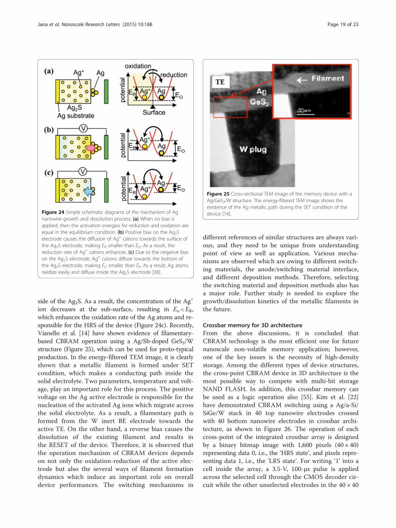
Figure 24 Simple schematic diagrams of the mechanism of Agnanowire growth and dissolution process. (a) When no bias isapplied, then the activation energies for reduction and oxidation areequal in the equilibrium condition. (b) Positive bias on the Ag2Selectrode causes the diffusion of Ag+ cations towards the surface ofthe Ag2S electrode, making ER smaller than EO. As a result, thereduction rate of Ag+ cations enhances. (c) Due to the negative biason the Ag2S electrode, Ag+ cations diffuse towards the bottom ofthe Ag2S electrode, making EO smaller than ER. As a result, Ag atomsoxidize easily and diffuse inside the Ag2S electrode [38].
Figure 25 Cross-sectional TEM image of the memory device with aAg/GeS2/W structure. The energy-filtered TEM image shows theexistence of the Ag metallic path during the SET condition of thedevice [14].
Jana et al. Nanoscale Research Letters (2015) 10:188 Page 19 of 23
side of the Ag2S. As a result, the concentration of the Ag+
ion decreases at the sub-surface, resulting in Eo < ER,which enhances the oxidation rate of the Ag atoms and re-sponsible for the HRS of the device (Figure 24c). Recently,Vianello et al. [14] have shown evidence of filamentary-based CBRAM operation using a Ag/Sb-doped GeS2/Wstructure (Figure 25), which can be used for proto-typicalproduction. In the energy-filtered TEM image, it is clearlyshown that a metallic filament is formed under SETcondition, which makes a conducting path inside thesolid electrolyte. Two parameters, temperature and volt-age, play an important role for this process. The positivevoltage on the Ag active electrode is responsible for thenucleation of the activated Ag ions which migrate acrossthe solid electrolyte. As a result, a filamentary path isformed from the W inert BE electrode towards theactive TE. On the other hand, a reverse bias causes thedissolution of the existing filament and results inthe RESET of the device. Therefore, it is observed thatthe operation mechanism of CBRAM devices dependson not only the oxidation-reduction of the active elec-trode but also the several ways of filament formationdynamics which induce an important role on overalldevice performances. The switching mechanisms in
different references of similar structures are always vari-ous, and they need to be unique from understandingpoint of view as well as application. Various mecha-nisms are observed which are owing to different switch-ing materials, the anode/switching material interface,and different deposition methods. Therefore, selectingthe switching material and deposition methods also hasa major role. Further study is needed to explore thegrowth/dissolution kinetics of the metallic filaments inthe future.
Crossbar memory for 3D architectureFrom the above discussions, it is concluded thatCBRAM technology is the most efficient one for futurenanoscale non-volatile memory application; however,one of the key issues is the necessity of high-densitystorage. Among the different types of device structures,the cross-point CBRAM device in 3D architecture is themost possible way to compete with multi-bit storageNAND FLASH. In addition, this crossbar memory canbe used as a logic operation also [55]. Kim et al. [22]have demonstrated CBRAM switching using a Ag/a-Si/SiGe/W stack in 40 top nanowire electrodes crossedwith 40 bottom nanowire electrodes in crossbar archi-tecture, as shown in Figure 26. The operation of eachcross-point of the integrated crossbar array is designedby a binary bitmap image with 1,600 pixels (40 × 40)representing data 0, i.e., the ‘HRS state’, and pixels repre-senting data 1, i.e., the ‘LRS state’. For writing ‘1’ into acell inside the array, a 3.5-V, 100-μs pulse is appliedacross the selected cell through the CMOS decoder cir-cuit while the other unselected electrodes in the 40 × 40
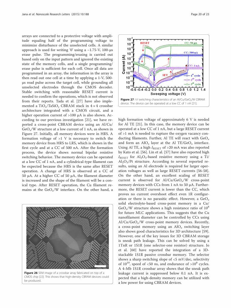
Figure 27 I-V switching characteristics of an Al/Cu/GeOx/W CBRAMdevice. The device can be operated at a low CC of 1 nA [21].
Jana et al. Nanoscale Research Letters (2015) 10:188 Page 20 of 23
arrays are connected to a protective voltage with ampli-tude equaling half of the programming voltage tominimize disturbance of the unselected cells. A similarapproach is used for writing ‘0’ using a −1.75-V, 100-μserase pulse. The programming/erasing is carried outbased only on the input pattern and ignored the existingstate of the memory cells, and a single programming/erase pulse is sufficient for each cell. Once all data areprogrammed in an array, the information in the array isthen read out one cell at a time by applying a 1-V, 500-μs read pulse across the target cell, while grounding allunselected electrodes through the CMOS decoder.Stable switching with reasonable RESET current isneeded to confirm the operations, which is not observedfrom their reports. Tada et al. [27] have also imple-mented a TiOx/TaSiOy CBRAM stack in 4 × 4 crossbararchitecture integrated with a CMOS circuit, and ahigher operation current of >100 μA is also shown. Ac-cording to our previous investigation [21], we have re-ported a cross-point CBRAM device using an Al/Cu/GeOx/W structure at a low current of 1 nA, as shown inFigure 27. Initially, all memory devices were in HRS. Aformation voltage of >1 V is necessary to switch thememory device from HRS to LRS, which is shown in thefirst cycle and at a CC of 500 nA. After the formationprocess, the device shows normal bipolar resistiveswitching behavior. The memory device can be operatedat a low CC of 1 nA, and a cylindrical-type filament canbe expected because the HRS is the same after RESEToperation. A change of HRS is observed at a CC of50 μA. At a higher CC of 50 μA, the filament diameteris increased and the shape of the filament will be a con-ical type. After RESET operation, the Cu filament re-mains at the GeOx/W interface. On the other hand, a
Figure 26 SEM image of a crossbar array fabricated on top of aCMOS chip [22]. This shows that high-density CBRAM devices couldbe produced.
high formation voltage of approximately 6 V is neededfor Al TE [21]. In this case, the memory device can beoperated at a low CC of 1 nA, but a large RESET currentof >1 mA is needed to rupture the oxygen vacancy con-ducting filaments. Further, Al TE will react with GeOx
and form an AlOx layer at the Al TE/GeOx interface.Using Al TE, a high IRESET of >20 mA was also reportedby Kato et al. [56]. Lin et al. [57] have also reported highIRESET for Al2O3-based resistive memory using a Ti/Al2O3/Pt structure. According to several reported re-sults, using an Al electrode is required for larger oper-ation voltages as well as large RESET currents [56-58].On the other hand, an excellent scaling of RESETcurrent is observed for Al/Cu/GeOx/W cross-pointmemory devices with CCs from 1 nA to 50 μA. Further-more, the RESET current is lower than the CC, whichproves no current overshoot effect even 1R configur-ation or there is no parasitic effect. However, a GeOx
solid electrolyte-based cross-point memory in a Cu/GeOx/W structure shows a high resistance ratio of 108
for future MLC applications. This suggests that the Cunanofilament diameter can be controlled by CCs usingAl/Cu/GeOx/W cross-point memory devices. Recently,a cross-point memory using an AlOx switching layeralso shows good characteristics for 3D architecture [59].However, one of the key issues for 3D CBRAM storageis sneak path leakage. This can be solved by using a1TnR or 1S1R (one selector-one resistor) structure. Joet al. [60] have reported the integration of a 3D-stackable 1S1R passive crossbar memory. The selectorshows a sharp switching slope of <5 mV/dec, selectivityof 1010, speed of <50 ns, and endurance of >108 cycles.A 4-Mb 1S1R crossbar array shows that the sneak pathleakage current is suppressed below 0.1 nA. It is ex-pected that a high-density memory can be utilized witha low power for using CBRAM devices.
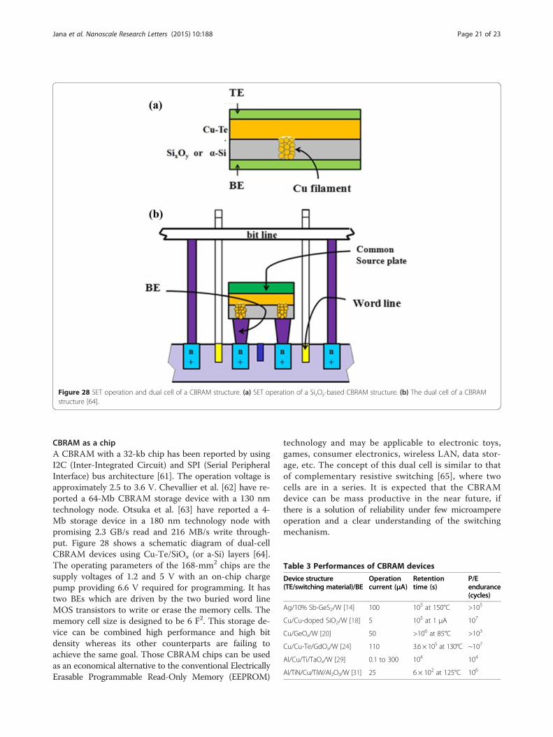
Figure 28 SET operation and dual cell of a CBRAM structure. (a) SET operation of a SixOy-based CBRAM structure. (b) The dual cell of a CBRAMstructure [64].
Table 3 Performances of CBRAM devices
Device structure(TE/switching material)/BE
Operationcurrent (μA)
Retentiontime (s)
P/Eendurance(cycles)
Ag/10% Sb-GeS2/W [14] 100 105 at 150°C >105
Cu/Cu-doped SiO2/W [18] 5 105 at 1 μA 107
Cu/GeOx/W [20] 50 >106 at 85°C >103
Cu/Cu-Te/GdOx/W [24] 110 3.6 × 10⁵ at 130°C ~107
Al/Cu/Ti/TaOx/W [29] 0.1 to 300 104 104
Al/TiN/Cu/TiW/Al2O3/W [31] 25 6 × 10² at 125°C 106
Jana et al. Nanoscale Research Letters (2015) 10:188 Page 21 of 23
CBRAM as a chipA CBRAM with a 32-kb chip has been reported by usingI2C (Inter-Integrated Circuit) and SPI (Serial PeripheralInterface) bus architecture [61]. The operation voltage isapproximately 2.5 to 3.6 V. Chevallier et al. [62] have re-ported a 64-Mb CBRAM storage device with a 130 nmtechnology node. Otsuka et al. [63] have reported a 4-Mb storage device in a 180 nm technology node withpromising 2.3 GB/s read and 216 MB/s write through-put. Figure 28 shows a schematic diagram of dual-cellCBRAM devices using Cu-Te/SiOx (or a-Si) layers [64].The operating parameters of the 168-mm2 chips are thesupply voltages of 1.2 and 5 V with an on-chip chargepump providing 6.6 V required for programming. It hastwo BEs which are driven by the two buried word lineMOS transistors to write or erase the memory cells. Thememory cell size is designed to be 6 F2. This storage de-vice can be combined high performance and high bitdensity whereas its other counterparts are failing toachieve the same goal. Those CBRAM chips can be usedas an economical alternative to the conventional ElectricallyErasable Programmable Read-Only Memory (EEPROM)
technology and may be applicable to electronic toys,games, consumer electronics, wireless LAN, data stor-age, etc. The concept of this dual cell is similar to thatof complementary resistive switching [65], where twocells are in a series. It is expected that the CBRAMdevice can be mass productive in the near future, ifthere is a solution of reliability under few microampereoperation and a clear understanding of the switchingmechanism.
Jana et al. Nanoscale Research Letters (2015) 10:188 Page 22 of 23
ConclusionsIn this article, we have reviewed CBRAM switchingcharacteristics and switching mechanism, introducingchalcogenide, oxide, and bilayer switching layers. In thefirst section, we review the switching performance ofchalcogenide-based CBRAM. It is observed that achalcogenide-based memory device shows good bipolarresistive switching, long P/E endurance of >105 cycles,and a good data retention of >105 s at >85°C. The mem-ory device also shows multi-level operation with varyingcurrent compliance from CCs of 5 to 500 μA. It is ob-served that the oxide-based memory device performs ata low CC of 5 pA, good device-to-device uniformity,good data retention at low current of 1 μA, and good P/E cycles as well. It is found that bilayer switching mate-rials show excellent device-to-device uniformity, robustdata retention, and better P/E cycles of >107 with a highspeed of few nanoseconds. The performances of CBRAMdevices using different switching materials and structuresare listed in Table 3. The switching mechanism is basedon the formation and dissolution of the metallic filamentdepending upon electrical bias. The growth kinetics ofthe metallic path in different chalcogenide- and oxide-based switching materials are reported. However, it isstill debated how to start growing/dissolving the me-tallic filament and which interface is responsible fordifferent switching materials and structures also. It issuggested that further study is needed for the under-standing of the switching mechanism. The cross-pointmemory in 3D architecture can have a promisingsolution for future high-density non-volatile memorywith low power. CBRAM as a chip is showing torealize mass production in the future. However, thereliability issues in terms of stability of HRS, LRS,endurance, and data retention need to be solved andmore studies are needed. It is expected that CBRAMdevices have very good opportunity for scaled (<11 nmtechnology node) non-volatile memory devices or logicgate operations.
Competing interestsThe authors declare that they have no competing interests.
Authors’ contributionsDJ, SR, RP, and MD reviewed all the published papers and prepared the firstdraft under the instruction of SM. SZR measured some of the devices, andRM reviewed some of the papers. This review paper was supervised by bothRM and SM. All authors contributed to the revision of the manuscript, andthey approved it for publication.
AcknowledgementsThis work was supported by the National Science Council (NSC), Taiwan, undercontract numbers NSC-97-2221-E-182-051-MY3, 98-2923-E-182-001-MY3,98-2221-E-182-052-MY3, 101-2221-E-182-061, and 102-2221-E-182-057-MY2.The name of the NSC has been changed to Ministry of Science and Technology(MOST), Taiwan.
Author details1Thin Film Nano Tech. Lab., Department of Electronic Engineering, ChangGung University, 259 Wen-Hwa 1st Rd., Kwei-Shan, Tao-Yuan 333, Taiwan.2Department of Electronics and Communication Engineering, NationalInstitute of Technology, Durgapur 713 209, India.
Received: 28 January 2015 Accepted: 24 March 2015
References1. Hutchby J, Garner M. Assessment of the potential & maturity of selected
emerging research memory technologies. Workshop & ERD/ERM WorkingGroup Meeting (April 6–7, 2010). 2010. http://www.itrs.net/Links/2010ITRS/2010Update/ToPost/ERD_ERM_2010FINALReportMemoryAssessment_ITRS.pdf
2. Waser R, Aono M. Nanoionics-based resistive switching memories. NatMater. 2007;6:833.
3. Wong HSP, Lee HY, Yu S, Chen YS, Wu Y, Chen PS, et al. Metal-oxide RRAM.Proc IEEE. 2012;100:1951.
4. Chen A, Haddad S, Wu YC, Fang TN, Lan Z, Avanzino S, et al. Non-volatileresistive switching for advanced memory applications. In: Tech. Dig.-Int.Electron Devices Meet., Washington, DC, MD, 2005, p. 746.
5. Prakash A, Jana D, Maikap S. TaOx-based resistive switching memories:prospective and challenges. Nanoscale Res Lett. 2013;8:418.
6. Hirose Y, Hirose H. Polarity-dependent memory switching and behavior ofAg dendrite in Ag-photodoped amorphous As2S3 films. J Appl Phys.1976;47:2767.
7. Kozicki MN, Yun M, Hilt L, Singh A. Applications of programmable resistancechanges in metal-doped chalcogenides. Pennington, NJ, USA: Electrochem.Soc; 1999. p. 298.
8. Terabe K, Hasegawa T, Nakayama T, Aono M. Quantized conductanceatomic switch. Nature. 2005;433:47.
9. Kund M, Beitel G, Pinnow CU, Röhr T, Schumann J, Symanczyk R, et al.Conductive-bridging RAM (CBRAM): an emerging non-volatile memorytechnology scalable to sub 20 nm. In: Tech. Dig.-Int. Electron Devices Meet.,Washington, DC, MD, 2005, p. 754.
10. Kozicki MN, Park M, Mitkova M. Nanoscale memory elements based onsolid-electrolytes. IEEE Trans Nanotech. 2005;4:331.
11. Schindler C, Meier M, Waser R, Kozicki MN. Resistive switching in Ag-Ge-Sewith extremely low write currents. Non-Volatile Memory TechnologySymposium (NVMTS), 2007, p. 82.
12. Rahaman SZ, Maikap S, Das A, Prakash A, Wu Y, Lai CS, et al. Enhancednanoscale resistive switching memory characteristics and switchingmechanism using high-Ge-content Ge0.5Se0.5 solid electrolyte. NanoscaleRes Lett. 2012;7:614.
13. Kozicki MN, Balakrishnan M, Gopalan C, Ratnakumar C, Mitkova M.Programmable metallization cell memory based on Ag-Ge-S and Cu-Ge-Ssolid electrolytes. Non-Volatile Memory Technology Symposium (NVMTS),2005, p. 83.
14. Vianello E, Molas G, Longnos F, Blaise P, Souchier E, Cagil C, et al. Sb-dopedGeS2 as performance and reliability booster in conductive bridge RAM. In:Tech. Dig.-Int. Electron Devices Meet., 2012, p. 31.5.1.
15. Choi SJ, Lee JH, Bae HJ, Yang WY, Kim TW, Kim KH. Improvement of CBRAMresistance window by scaling down electrode size in pure-GeTe film. IEEEElectron Device Lett. 2009;30:120.
16. Banno N, Sakamoto T, Iguchi N, Sunamura H, Terabe K, Hasegawa T, et al.Diffusivity of Cu ions in solid electrolyte and its effect on the performanceof nanometer-scale switch. IEEE Trans Electron Devices. 2008;55:3283.
17. Maikap S, Rahaman SZ, Wu TY, Chen F, Kao MJ, Tsai MJ. Low current (5 pA)resistive switching memory using high-κ Ta2O5 solid-electrolyte. IEEEEuropean Solid-State Device Conference, 2009, p. 217.
18. Schindler C, Thermadam SCP, Waser R, Kozicki MN. Bipolar and unipolarresistive switching in Cu-doped SiO2. IEEE Trans Electron Devices.2007;54:2762.
19. Li Y, Long S, Zhang M, Liu Q, Shao L, Zhang S, et al. Resistive switchingproperties of Au/ZrO2/Ag structure for low-voltage nonvolatile memoryapplications. IEEE Electron Device Lett. 2010;31:117.
20. Rahaman SZ, Maikap S, Chen WS, Lee HY, Chen FT, Kao MJ, et al.Repeatable unipolar/bipolar resistive memory characteristics and switchingmechanism using a Cu nanofilament in a GeOx film. Appl Phys Lett.2012;101:073106.
Jana et al. Nanoscale Research Letters (2015) 10:188 Page 23 of 23
21. Rahaman SZ, Maikap S. Comparison of resistive switching characteristicsusing copper and aluminum electrodes on GeOx/W cross-point memories.Nanoscale Res Lett. 2013;8:509.
22. Kim KH, Gaba S, Wheeler D, Cruz-Albrecht JM, Hussain T, Srinivasa N, et al. Afunctional hybrid memristor crossbar-array/CMOS system for data storageand neuromorphic applications. Nano Lett. 2012;12:389.
23. Sun B, Liu LF, Wang Y, Han DD, Liu X Y, Han RQ, et al. Bipolar resistiveswitching behaviors of Ag/Si3N4/Pt memory device. In: Tech Dig.-Solid-Stateand Integrated-Circuit Technology, 2008, p. 925.
24. Aratani K, Ohba K, Mizuguchi T, Yasuda S, Shiimoto T, Tsushima T, et al. Anovel resistance memory with high scalability and nanosecond switching.In: Tech Dig.-International Electron Devices Meet., 2007, p. 783.
25. Zahurak J, Miyata K, Fischer M, Balakrishnan M, Chhajed S, Wells D, et al.Process integration of a 27nm, 16Gb Cu ReRAM. In: Tech. Dig.-Int. ElectronDevices Meet., 2014, p. 140.
26. Yoon J, Choi H, Lee D, Park JB, Lee J, Seong DJ, et al. Excellent switchinguniformity of Cu-doped MoOx/GdOx bilayer for nonvolatile memoryapplications. IEEE Electron Device Lett. 2009;30:457.
27. Tada M, Sakamoto T, Banno N, Aono M, Hada H, Kasai N. Nonvolatilecrossbar switch using TiOx/TaSiOy solid-electrolyte. IEEE Trans ElectronDevices. 2010;57:1987.
28. Rahaman SZ, Maikap S, Chen WS, Lee HY, Chen F, Tien TC, et al. Impact ofTaOx nanolayer at the GeSex/W interface on resistive switching memoryperformance and investigation of Cu nanofilament. J Appl Phys.2012;111:063710.
29. Rahaman SZ, Maikap S, Tien TC, Lee HY, Chen WS, Chen FT, et al. Excellentresistive memory characteristics and switching mechanism using a Tinanolayer at the Cu/TaOx interface. Nanoscale Res Lett. 2012;7:345.
30. Goux L, Opsomer K, Degraeve R, Müller R, Detavernier C, Wouters DJ, et al.Influence of the Cu-Te composition and microstructure on the resistiveswitching of Cu-Te/Al2O3/Si cells. Appl Phys Lett. 2011;99:053502.
31. Belmonte A, Kim W, Chan BT, Heylen N, Fantini A, Houssa M, et al.90 nm W/Al2O3/TiW/Cu 1T1R CBRAM cell showing low-power, fast anddisturb-free operation. IEEE International Memory Workshop, 2013, p. 26.
32. Devulder W, Opsomer K, Seidel F, Belmonte A, Muller R, Schutter BD, et al.Influence of carbon alloying on the thermal stability and resistive switchingbehavior of copper-telluride based CBRAM cells. ACS Appl Mater Interfaces.2013;5:6984.
33. Rahaman SZ, Maikap S, Chiu HC, Lin CH, Wu TY, Chen YS, et al. Bipolarresistive switching memory using Cu metallic filament in Ge0.4Se0.6 solid-electrolyte. Electrochem Solid-State Lett. 2010;13:H159.
34. Ueno T, Odajima A. Study of photo-induced effect in obliquely-depositedamorphous Ge-Se films by XPS. Jpn J Appl Phys. 1980;19:L519.
35. Ueno T, Odajima A. X-ray photoelectron spectroscopy of Ag-and Cu-dopedamorphous As2Se3 and GeSe2. Jpn J Appl Phys. 1982;21:230.
36. Moulder JF, Stickle WF, Sobol PE, Bomben KD. Handbook of x-ray photo-electron spectroscopy. Eden Prairie, MN: Perkin-Elmer Corp; 1992.
37. Liaw C, Kund M, Landsiedel DS, Ruge I. The conductive bridging randomaccess memory (CBRAM): a non-volatile multi-level memory technology.IEEE European Solid-State Device Conference (ESSDERC), 2007, p. 226.
38. Hasegawa T, Terabe K, Tsuruoka T, Aono M. Atomic switch: atom/ionmovement controlled devices for beyond Von-Neumann computers. AdvMater. 2012;24:252.
39. Schindler C, Staikov G, Waser R. Electrode kinetics of Cu–SiO2-based resistiveswitching cells: overcoming the voltage-time dilemma of electrochemicalmetallization memories. Appl Phys Lett. 2009;94:072109.
40. Rahaman SZ, Maikap S, Chiu HC, Lin CH, Wu TY, Chen YS, et al. Low poweroperation of resistive switching memory device using novel W/Ge0.4Se0.6/Cu/Al structure. IEEE International Memory Workshop (IMW), 2009.
41. Jameson JR, Blanchard P, Cheng C, Dinh J, Gallo A, Gopalakrishnan V, et al.Conductive-bridge memory (CBRAM) with excellent high-temperatureretention. In: Tech. Dig.-Int. Electron Devices Meet., 2013, p. 30-1.
42. Russo U, Kamalanathan D, Ielmini D, Lacaita AL, Kozicki MN. Study ofmultilevel programming in programmable metallization cell (PMC) memory.IEEE Trans Electron Devices. 2009;56:1040.
43. Sakamoto T, Lister K, Banno N, Hasegawa T, Terabe K, Aono M. Electronictransport in Ta2O5 resistive switch. Appl Phys Lett. 2007;91:092110.
44. Schindler C, Weides M, Kozicki M, Waser R. Low current resistive switchingin Cu–SiO2 cells. Appl Phys Lett. 2008;92:122910.
45. Tsunoda K, Fukuzumi Y, Jameson JR, Wang Z, Griffin PB, Nishi Y. Bipolarresistive switching in polycrystalline TiO2 films. Appl Phys Lett.2007;90:113501.
46. Liu Q, Long S, Lv H, Wang W, Niu J, Huo Z, et al. Controllable growth ofnanoscale conductive filaments in solid-electrolyte-based ReRAM by using ametal nanocrystal covered bottom electrode. ACS Nano. 2010;4:6162.
47. Sakamoto T, Banno N, Iguchi N, Kawaura H, Sunmura H, Fujieda S, et al. ATa2O5 solid-electrolyte switch with improved reliability. Symp. on VLSITechno., 2007, p. 38.
48. Balakrishnan M, Thermadam SCP, Mitkova M, Kozicki. A low power non-volatile memory element based on copper in deposited silicon oxide. Non-Volatile Memory Technology Symposium (NVMTS), 2006, p. 104.
49. Guy J, Molas G, Vianello E, Longnos F, Blanc S, Carabasse C, et al.Investigation of the physical mechanisms governing data-retention in downto 10 nm nano-trench Al2O3/CuTeGe conductive bridge RAM (CBRAM). In:Tech. Dig.-Int. Electron Devices Meet., 2013, p. 30.2.2.
50. Symanczyk R, Balakrishnan M, Gopalan C, Happ T, Kozicki M, Kund M, et al.Electrical characterization of solid state ionic memory elements. Proceedingsof the Non-Volatile Memory Technology Symposium, 2003, p. 17-1.
51. McHardy C, Fitzgerald A, Moir P, Flynn M. The dissolution of metals inamorphous chalcogenides and the effects of electron and ultravioletradiation. J Phys C Solid State Phys. 1987;20:4055.
52. Phillips JC. Structural principles of alpha-AgI and related double salts.J Electrochem Soc. 1976;123:934.
53. Schindler C, Szot K, Karthäuser S, Waser R. Controlled local filament growthand dissolution in Ag-Ge-Se. Phys Status Solidi Rapid Res Lett. 2008;2:129.
54. Yang Y, Gao P, Gaba S, Chang T, Pan X, Lu W. Observation of conductingfilament growth in nanoscale resistive memories. Nat Commun. 2012;3:732.
55. Borghetti J, Snider GS, Kuekes PJ, Yang JJ, Stewart DR, Williams RS.Memristive switches enable stateful logic operations via materialimplication. Nature. 2010;464:873.
56. Kato S, Nigo S, Lee JW, Mihalik M, Kitazawa H, Kido G. Transport propertiesof anodic porous alumina for ReRAM. J Phys Conf Ser. 2008;109:012017.
57. Lin CY, Wu CY, Wu CY, Lee TC, Yang FL, Hu C, et al. Effect of top electrodematerial on resistive switching properties of ZrO2 film memory devices. IEEEElectron Device Lett. 2007;28:366.
58. Rahaman SZ, Maikap S, Ray SK, Lee HY, Chen WS, Chen F, et al. Recordresistance ratio and bipolar/unipolar resistive switching characteristics ofmemory device using germanium oxide solid-electrolyte. Jpn J Appl Phys.2012;51:04DD11.
59. Maikap S, Panja R, Jana D. Copper pillar and memory characteristics usingAl2O3 switching material for 3D architecture. Nanoscale Res Lett. 2014;9:366.
60. Jo SH, Kumar T, Narayanan S, Lu WD, Nazarian H. 3D-stackable crossbar resistivememory based on field assisted superlinear threshold (FAST) selector. In: Tech.Dig.-Int. Electron Devices Meet. (IEDM), 2014, p. 160.
61. Gopinath VP. http://sites.ieee.org/sfbanano/files/2013/11/PG_IEEE-Talk-Adesto_CBRAM_20131217_rev4_send.pdf (http://www.adestotech.com/cbram).
62. Chevallier CJ, Siau CH, Lim SF, Namala SR, Matsuoka M, Bateman BL, et al. A0.13 μm 64Mb multi-layered conductive metal-oxide memory. IEEEInternational Solid-State Circuits Conference, 2010, p. 260.
63. Otsuka W, Miyata K, Kitagawa M, Tsutsui K, Tsushima T, Yoshihara H, et al. A4 Mb conductive-bridge resistive memory with 2.3GB/s read-throughputand 216 MB/s program-throughput. IEEE International Solid-State CircuitsConference, 2011, p. 210.
64. Neale R. Showtime for the Micron-Sony 16Gb ReRAM. 2014. http://www.ee-times.com/author.asp?section_id=36&doc_id=1321276.
65. Linn E, Rosezin R, Kugeler C, Waser R. Complementary resistive switches forpassive nanocrossbar memories. Nat Mater. 2010;9:403.